JP2013536551A - Support having scattering layer for organic light emitting diode device, organic light emitting device including the support - Google Patents
Support having scattering layer for organic light emitting diode device, organic light emitting device including the supportDownload PDFInfo
- Publication number
- JP2013536551A JP2013536551AJP2013523653AJP2013523653AJP2013536551AJP 2013536551 AJP2013536551 AJP 2013536551AJP 2013523653 AJP2013523653 AJP 2013523653AJP 2013523653 AJP2013523653 AJP 2013523653AJP 2013536551 AJP2013536551 AJP 2013536551A
- Authority
- JP
- Japan
- Prior art keywords
- scattering
- scattering layer
- organic light
- binder
- substrate
- Prior art date
- Legal status (The legal status is an assumption and is not a legal conclusion. Google has not performed a legal analysis and makes no representation as to the accuracy of the status listed.)
- Pending
Links
Images


Classifications
- C—CHEMISTRY; METALLURGY
- C03—GLASS; MINERAL OR SLAG WOOL
- C03C—CHEMICAL COMPOSITION OF GLASSES, GLAZES OR VITREOUS ENAMELS; SURFACE TREATMENT OF GLASS; SURFACE TREATMENT OF FIBRES OR FILAMENTS MADE FROM GLASS, MINERALS OR SLAGS; JOINING GLASS TO GLASS OR OTHER MATERIALS
- C03C3/00—Glass compositions
- C03C3/04—Glass compositions containing silica
- C03C3/062—Glass compositions containing silica with less than 40% silica by weight
- C03C3/064—Glass compositions containing silica with less than 40% silica by weight containing boron
- C03C3/066—Glass compositions containing silica with less than 40% silica by weight containing boron containing zinc
- C—CHEMISTRY; METALLURGY
- C03—GLASS; MINERAL OR SLAG WOOL
- C03C—CHEMICAL COMPOSITION OF GLASSES, GLAZES OR VITREOUS ENAMELS; SURFACE TREATMENT OF GLASS; SURFACE TREATMENT OF FIBRES OR FILAMENTS MADE FROM GLASS, MINERALS OR SLAGS; JOINING GLASS TO GLASS OR OTHER MATERIALS
- C03C17/00—Surface treatment of glass, not in the form of fibres or filaments, by coating
- C03C17/006—Surface treatment of glass, not in the form of fibres or filaments, by coating with materials of composite character
- C03C17/007—Surface treatment of glass, not in the form of fibres or filaments, by coating with materials of composite character containing a dispersed phase, e.g. particles, fibres or flakes, in a continuous phase
- C—CHEMISTRY; METALLURGY
- C03—GLASS; MINERAL OR SLAG WOOL
- C03C—CHEMICAL COMPOSITION OF GLASSES, GLAZES OR VITREOUS ENAMELS; SURFACE TREATMENT OF GLASS; SURFACE TREATMENT OF FIBRES OR FILAMENTS MADE FROM GLASS, MINERALS OR SLAGS; JOINING GLASS TO GLASS OR OTHER MATERIALS
- C03C17/00—Surface treatment of glass, not in the form of fibres or filaments, by coating
- C03C17/34—Surface treatment of glass, not in the form of fibres or filaments, by coating with at least two coatings having different compositions
- C03C17/42—Surface treatment of glass, not in the form of fibres or filaments, by coating with at least two coatings having different compositions at least one coating of an organic material and at least one non-metal coating
- H—ELECTRICITY
- H10—SEMICONDUCTOR DEVICES; ELECTRIC SOLID-STATE DEVICES NOT OTHERWISE PROVIDED FOR
- H10K—ORGANIC ELECTRIC SOLID-STATE DEVICES
- H10K50/00—Organic light-emitting devices
- H10K50/80—Constructional details
- H—ELECTRICITY
- H10—SEMICONDUCTOR DEVICES; ELECTRIC SOLID-STATE DEVICES NOT OTHERWISE PROVIDED FOR
- H10K—ORGANIC ELECTRIC SOLID-STATE DEVICES
- H10K50/00—Organic light-emitting devices
- H10K50/80—Constructional details
- H10K50/85—Arrangements for extracting light from the devices
- H—ELECTRICITY
- H10—SEMICONDUCTOR DEVICES; ELECTRIC SOLID-STATE DEVICES NOT OTHERWISE PROVIDED FOR
- H10K—ORGANIC ELECTRIC SOLID-STATE DEVICES
- H10K50/00—Organic light-emitting devices
- H10K50/80—Constructional details
- H10K50/85—Arrangements for extracting light from the devices
- H10K50/854—Arrangements for extracting light from the devices comprising scattering means
- C—CHEMISTRY; METALLURGY
- C03—GLASS; MINERAL OR SLAG WOOL
- C03C—CHEMICAL COMPOSITION OF GLASSES, GLAZES OR VITREOUS ENAMELS; SURFACE TREATMENT OF GLASS; SURFACE TREATMENT OF FIBRES OR FILAMENTS MADE FROM GLASS, MINERALS OR SLAGS; JOINING GLASS TO GLASS OR OTHER MATERIALS
- C03C2217/00—Coatings on glass
- C03C2217/40—Coatings comprising at least one inhomogeneous layer
- C03C2217/43—Coatings comprising at least one inhomogeneous layer consisting of a dispersed phase in a continuous phase
- C03C2217/44—Coatings comprising at least one inhomogeneous layer consisting of a dispersed phase in a continuous phase characterized by the composition of the continuous phase
- C03C2217/45—Inorganic continuous phases
- C03C2217/452—Glass
- C—CHEMISTRY; METALLURGY
- C03—GLASS; MINERAL OR SLAG WOOL
- C03C—CHEMICAL COMPOSITION OF GLASSES, GLAZES OR VITREOUS ENAMELS; SURFACE TREATMENT OF GLASS; SURFACE TREATMENT OF FIBRES OR FILAMENTS MADE FROM GLASS, MINERALS OR SLAGS; JOINING GLASS TO GLASS OR OTHER MATERIALS
- C03C2217/00—Coatings on glass
- C03C2217/40—Coatings comprising at least one inhomogeneous layer
- C03C2217/43—Coatings comprising at least one inhomogeneous layer consisting of a dispersed phase in a continuous phase
- C03C2217/46—Coatings comprising at least one inhomogeneous layer consisting of a dispersed phase in a continuous phase characterized by the dispersed phase
- C—CHEMISTRY; METALLURGY
- C03—GLASS; MINERAL OR SLAG WOOL
- C03C—CHEMICAL COMPOSITION OF GLASSES, GLAZES OR VITREOUS ENAMELS; SURFACE TREATMENT OF GLASS; SURFACE TREATMENT OF FIBRES OR FILAMENTS MADE FROM GLASS, MINERALS OR SLAGS; JOINING GLASS TO GLASS OR OTHER MATERIALS
- C03C2218/00—Methods for coating glass
- C03C2218/30—Aspects of methods for coating glass not covered above
- C03C2218/365—Coating different sides of a glass substrate
- H—ELECTRICITY
- H10—SEMICONDUCTOR DEVICES; ELECTRIC SOLID-STATE DEVICES NOT OTHERWISE PROVIDED FOR
- H10K—ORGANIC ELECTRIC SOLID-STATE DEVICES
- H10K2102/00—Constructional details relating to the organic devices covered by this subclass
- H10K2102/301—Details of OLEDs
- H10K2102/331—Nanoparticles used in non-emissive layers, e.g. in packaging layer
- Y—GENERAL TAGGING OF NEW TECHNOLOGICAL DEVELOPMENTS; GENERAL TAGGING OF CROSS-SECTIONAL TECHNOLOGIES SPANNING OVER SEVERAL SECTIONS OF THE IPC; TECHNICAL SUBJECTS COVERED BY FORMER USPC CROSS-REFERENCE ART COLLECTIONS [XRACs] AND DIGESTS
- Y10—TECHNICAL SUBJECTS COVERED BY FORMER USPC
- Y10T—TECHNICAL SUBJECTS COVERED BY FORMER US CLASSIFICATION
- Y10T428/00—Stock material or miscellaneous articles
- Y10T428/24—Structurally defined web or sheet [e.g., overall dimension, etc.]
- Y10T428/24355—Continuous and nonuniform or irregular surface on layer or component [e.g., roofing, etc.]
- Y—GENERAL TAGGING OF NEW TECHNOLOGICAL DEVELOPMENTS; GENERAL TAGGING OF CROSS-SECTIONAL TECHNOLOGIES SPANNING OVER SEVERAL SECTIONS OF THE IPC; TECHNICAL SUBJECTS COVERED BY FORMER USPC CROSS-REFERENCE ART COLLECTIONS [XRACs] AND DIGESTS
- Y10—TECHNICAL SUBJECTS COVERED BY FORMER USPC
- Y10T—TECHNICAL SUBJECTS COVERED BY FORMER US CLASSIFICATION
- Y10T428/00—Stock material or miscellaneous articles
- Y10T428/249921—Web or sheet containing structurally defined element or component
- Y10T428/249953—Composite having voids in a component [e.g., porous, cellular, etc.]
- Y10T428/249967—Inorganic matrix in void-containing component
- Y10T428/249969—Of silicon-containing material [e.g., glass, etc.]
- Y—GENERAL TAGGING OF NEW TECHNOLOGICAL DEVELOPMENTS; GENERAL TAGGING OF CROSS-SECTIONAL TECHNOLOGIES SPANNING OVER SEVERAL SECTIONS OF THE IPC; TECHNICAL SUBJECTS COVERED BY FORMER USPC CROSS-REFERENCE ART COLLECTIONS [XRACs] AND DIGESTS
- Y10—TECHNICAL SUBJECTS COVERED BY FORMER USPC
- Y10T—TECHNICAL SUBJECTS COVERED BY FORMER US CLASSIFICATION
- Y10T428/00—Stock material or miscellaneous articles
- Y10T428/249921—Web or sheet containing structurally defined element or component
- Y10T428/249953—Composite having voids in a component [e.g., porous, cellular, etc.]
- Y10T428/249967—Inorganic matrix in void-containing component
- Y10T428/24997—Of metal-containing material
Landscapes
- Chemical & Material Sciences (AREA)
- General Chemical & Material Sciences (AREA)
- Life Sciences & Earth Sciences (AREA)
- Engineering & Computer Science (AREA)
- Chemical Kinetics & Catalysis (AREA)
- Geochemistry & Mineralogy (AREA)
- Materials Engineering (AREA)
- Organic Chemistry (AREA)
- Optics & Photonics (AREA)
- Physics & Mathematics (AREA)
- Dispersion Chemistry (AREA)
- Composite Materials (AREA)
- Electroluminescent Light Sources (AREA)
Abstract
Translated fromJapaneseDescription
Translated fromJapanese本発明は、有機発光ダイオードデバイスのための支持体に関する。より詳しく言えば、散乱層で被覆された透明ガラス基材を含む有機発光ダイオードデバイスのための支持体と、そのようなデバイスとに関する。 The present invention relates to a support for organic light emitting diode devices. More particularly, it relates to a support for an organic light emitting diode device comprising a transparent glass substrate coated with a scattering layer, and such a device.
OLED(有機発光ダイオード)は、有機エレクトロルミネッセント材料、又は有機エレクトロルミネッセント材料の積重体を含み、そして2つの電極を備えおり、これらの電極のうちの、下部電極と称され、一般にアノードである一方の電極は、ガラス基材と結合されたものからなり、上部電極と称され、一般にカソードである他方の電極は、有機発光システムの上に配置される。 An OLED (Organic Light Emitting Diode) comprises an organic electroluminescent material, or a stack of organic electroluminescent materials, and comprises two electrodes, of these electrodes, commonly referred to as the bottom electrode, One electrode, which is the anode, consists of a glass substrate and is referred to as the top electrode, and the other electrode, which is generally the cathode, is placed on top of the organic light emitting system.
OLEDは、アノードから注入される正孔とカソードから注入される電子の再結合エネルギーを利用するエレクトロルミネッセンスにより光を放出するデバイスである。 An OLED is a device that emits light by electroluminescence using the recombination energy of holes injected from an anode and electrons injected from a cathode.
次のように、いろいろなOLEDの構成が存在している。
・下部放射デバイス、すなわち(半)透明下部電極と反射性上部電極とを備えたデバイス。
・上部照射デバイス、すなわち(半)透明上部電極と反射性下部電極とを備えたデバイス。
・上部及び下部放射デバイス、すなわち(半)透明下部電極と(半)透明上部電極の両者を備えたデバイス。Various OLED configurations exist as follows.
A lower radiating device, ie a device with a (semi) transparent lower electrode and a reflective upper electrode
A top illumination device, ie a device with a (semi) transparent top electrode and a reflective bottom electrode.
-Top and bottom emitting devices, ie devices with both (semi) transparent bottom electrode and (semi) transparent top electrode.
本発明は、下部放射OLEDデバイスに関し、任意選択的に上部放射OLEDデバイスにも関する。 The present invention relates to bottom emitting OLED devices, and optionally to top emitting OLED devices.
OLEDには一般に、表示スクリーンにおける用途があり、つい最近では照明デバイスにおける用途がある。 OLEDs generally have applications in display screens, and more recently in lighting devices.
ランプタイプの照明装置について言うと、OLEDから取り出される光は、スペクトルの特定波長において、あるいは全てにおいて放射する「白色」光である。更に、この光は均一に放出されなければならない。これは、より正確に言えば、放射がランベルト的であること、すなわち全ての方向において測光ルミネッセンスが等しいことを特徴とすることによりランベルトの法則に従うことを意味する。 With respect to lamp-type lighting devices, the light extracted from the OLED is “white” light that radiates at a specific wavelength or all of the spectrum. Furthermore, this light must be emitted uniformly. This, more precisely, means that the radiation is Lambertian, that is, it follows Lambert's law by being characterized by equal photometric luminescence in all directions.
そうは言っても、OLEDの光抽出効率は低く、すなわちガラス基材から実際に出ていく光のエレクトロルミネッセント材料により放射されるそれに対する比は比較的小さく、ほぼ0.25である。 Nevertheless, the light extraction efficiency of the OLED is low, i.e. the ratio of the light actually leaving the glass substrate to that emitted by the electroluminescent material is relatively small, approximately 0.25.
この現象は、特に、屈折率が基材のガラス(n=1.5)とデバイスの外部の空気(n=1)とで異なることによるガラス基材内での光の反射によって説明される。 This phenomenon is explained in particular by the reflection of light within the glass substrate due to the difference in refractive index between the substrate glass (n = 1.5) and the air outside the device (n = 1).
更に、観測の角度の関数としての比色分析値の変動が、使用する有機エレクトロルミネッセント材料及び電極の積重体の性質に非常に強く依存することが観測された。よって、発光デバイスを特に照明源として使用するための照明の均一性の点から見た要件は、達成されていないようである。 Furthermore, it has been observed that the variation in colorimetric values as a function of the angle of observation is very strongly dependent on the nature of the organic electroluminescent material used and the electrode stack. Thus, the requirement in terms of illumination uniformity for using the light emitting device as a particularly illumination source does not appear to be achieved.
従って、OLEDの効率を向上させるための、すなわちできるだけ均一である白色光を提供するとともに抽出ゲインを増加させるための、解決策が模索されている。「均一」という用語は、以下においては、強度の均一性、色の均一性、及び空間における均一性を意味するものと理解される。 Accordingly, solutions are being sought for improving the efficiency of OLEDs, i.e. providing white light as uniform as possible and increasing extraction gain. The term “uniform” is understood in the following to mean intensity uniformity, color uniformity, and uniformity in space.
ここでは、ガラス−空気界面での、ガラス基材に関係する解決策に関心が寄せられ、それは幾何光学を必要とする。 Here, interest is focused on solutions involving glass substrates at the glass-air interface, which require geometric optics.
特にフランス国特許出願公開第2937467号明細書から知られているのが、無機ガラス基材が、第1の電極を支持する主面の反対側の主面に、無機バインダーとこのバインダー中に分散した散乱用粒子を含むとともに、このバインダー中に分散した波長範囲が325〜400nmの紫外(UV)線を吸収する粒子も含む散乱層を含むOLEDデバイスである。 In particular, it is known from FR 2937467 that an inorganic glass substrate is dispersed in an inorganic binder and in this binder on the main surface opposite to the main surface supporting the first electrode. And a scattering layer that also includes particles that absorb ultraviolet (UV) rays having a wavelength range of 325 to 400 nm dispersed in the binder.
バインダーは、ガラスフリット、あるいはケイ酸カリウム、ナトリウムもしくはリチウムから得られる。 The binder is obtained from glass frit or potassium, sodium or lithium silicate.
散乱用粒子は、アルミナ、あるいはBaSO4、ZrO2、SiO2又はCaCO3の粒子である。The scattering particles are alumina or BaSO4 , ZrO2 , SiO2 or CaCO3 particles.
バインダーの比率は、散乱層の総重量の30〜70%程度であり、散乱用粒子の比率は層の総重量の25〜60%程度であり、UV線を吸収する粒子の比率は層の総重量の2%と15%間である。 The ratio of the binder is about 30 to 70% of the total weight of the scattering layer, the ratio of the particles for scattering is about 25 to 60% of the total weight of the layer, and the ratio of particles that absorb UV rays is the total weight of the layer. Between 2% and 15% by weight.
厚さが11μmの散乱・UV防止層の好ましい例は、次のものである。
・52%の溶融ガラスフリット
・40%のアルミナ
・8%の紫外線吸収粒子、好ましくは4%のTiO2と4%のZnOPreferable examples of the scattering / UV preventing layer having a thickness of 11 μm are as follows.
52% molten glass frit 40% alumina 8% UV absorbing particles, preferably 4% TiO2 and 4% ZnO
散乱層は、スクリーン印刷又は任意の好適な技術、例えば塗布、溶液への浸漬(ディップコーティング)、スプレーなどにより、基材へ付加される。 The scattering layer is applied to the substrate by screen printing or any suitable technique such as coating, dipping in solution (dip coating), spraying, and the like.
この層の散乱機能は、白色光を形成する色の「再混合」を可能にし、これがはるかに均一な光を抽出するのを可能にする。 The scattering function of this layer allows for the “remixing” of the colors that form white light, which allows it to extract much more uniform light.
これはまた、デバイスに向かい合う観測者によって知覚される比色分析値の変動を低減するのも可能にする。 This also makes it possible to reduce the variation of the colorimetric values perceived by the observer facing the device.
しかし、このOLEDデバイスのスクラップ発生率は大きいことが分かった。 However, it has been found that the scrap generation rate of this OLED device is large.
本発明の目的は、特に、OLEDの光学的性能(特に光の抽出及び/又は、選択された放射多色光、特に白色光の観測の角度の関数としての比色分析値の変動の制限)を犠牲にすることなしに、又はそれらを向上さえさせて、あるいは生産上の問題を生じさせることなしに、堅牢なOLEDデバイスをうまく製造することである。 The object of the present invention is in particular the optical performance of the OLED (especially the limitation of the variation of the colorimetric values as a function of the angle of light extraction and / or observation of the selected polychromatic light, in particular white light). It is to successfully manufacture robust OLED devices without sacrificing, or even improving them, or causing production problems.
もう一つの重要な目的は、OLEDデバイスの製造プロセスとの相性のよいそのようなデバイスの製造を可能にすることである。 Another important objective is to enable the manufacture of such devices that are compatible with the manufacturing process of OLED devices.
本発明は、この目的のために、第1及び第2の向かい合った主面を備えた、無機ガラス製の透明基材であり、(本質的に)無機のバインダーとこのバインダー中に分散した散乱用構成要素とを含む散乱層でその第2面を(直接)被覆された基材を連続して含む有機発光ダイオードのための支持体であって、当該ガラス質のバインダーは40〜60wt%の酸化ビスマスBi2O3、あるいは45〜58wt%の酸化ビスマスBi2O3を含み、当該ガラス質バインダーの比率は前記散乱層の総重量の少なくとも20%である、有機発光ダイオードのための支持体を提案する。For this purpose, the present invention is a transparent substrate made of inorganic glass with first and second opposing major surfaces, and (essentially) an inorganic binder and scattering dispersed in the binder. A support for an organic light-emitting diode comprising a substrate having a (directly) coated second surface with a scattering layer comprising a structural component, wherein the glassy binder comprises 40-60 wt% Support for organic light emitting diodes comprising bismuth oxide Bi2 O3 or 45 to 58 wt% bismuth oxide Bi2 O3 , wherein the proportion of the vitreous binder is at least 20% of the total weight of the scattering layer Propose.
本発明による散乱層(単層又は多層)中の酸化ビスマスの前記好適な比率は、増進した耐薬品性を保証する。 The preferred ratio of bismuth oxide in the scattering layer (single layer or multilayer) according to the invention ensures enhanced chemical resistance.
しかし、OLED製造の状況の中で、散乱層を劣化させることがあり得る様々な工程が行われ、すなわち、
・基材の洗浄(通常、有機溶剤(エタノール、アセトン)又は塩基性溶液(一般に水酸化ナトリウム)を使用)、
・第1面上の第1の電極(基材に一番近いもの)のエッチング、
・エッチングしようとするパターンを画定するのに使用されるレジストの任意選択的な除去(通常、有機溶剤(エタノール、アセトン等)又は塩基性溶液(一般に水酸化ナトリウム)を使用)、
が行われる。However, in the context of OLED manufacturing, various processes are performed that can degrade the scattering layer, i.e.
・ Washing the substrate (usually using an organic solvent (ethanol, acetone) or a basic solution (generally sodium hydroxide)),
Etching the first electrode on the first surface (the one closest to the substrate)
Optional removal of the resist used to define the pattern to be etched (usually using an organic solvent (ethanol, acetone, etc.) or a basic solution (typically sodium hydroxide)),
Is done.
意外なことに、通常のフリットと違って、酸化ビスマスの含有量が多いそのバインダーを選定することによって、本発明による散乱層はOLEDの生産中に基材が被るこれらの種々の化学的処理に耐える。 Surprisingly, unlike ordinary frit, by selecting its binder with a high content of bismuth oxide, the scattering layer according to the present invention can be used for these various chemical treatments that the substrate undergoes during the production of OLEDs. Endure.
前記ガラス質のバインダーは、当業者がエナメル又は溶融ガラスフリットと呼ぶものでよい。 The glassy binder may be what the skilled person calls enamel or molten glass frit.
こうして、本発明による散乱層は、
・OLEDからの光の抽出を保全すること、
・OLED製造プロセスの種々の工程との相性がよいこと、
を可能にする。Thus, the scattering layer according to the invention is
-Preserve the light extraction from the OLED,
-Good compatibility with various steps of the OLED manufacturing process,
Enable.
散乱層は好ましくは、空気にむき出しの主たる外表面を有する。 The scattering layer preferably has a major outer surface exposed to air.
この明細書の全体を通して、本発明による基材は、第1面を下に向け、第1面に向き合った第2面を上に向けて、水平に横たわっているものと見なされ、よって「上」及び「下」との表現の意味するところはこの方向付けに関連して考えられるべきである。具体的に明記しない限り、「上」及び「下」との表現は、2つの構成要素が互いに接触した位置にあることを必ずしも意味するものではない。
「下部」及び「上部」という用語は、ここではこの位置づけに関連して使用される。Throughout this specification, a substrate according to the present invention is considered to lie horizontally, with the first side facing down and the second side facing the first side facing up. The meaning of the expressions "" and "below" should be considered in connection with this orientation. Unless specifically stated, the expressions “upper” and “lower” do not necessarily imply that the two components are in contact with each other.
The terms “lower” and “upper” are used herein in connection with this positioning.
この明細書を通して、「屈折率」という用語は、590nmの波長で測定される光学的屈折率を指す。 Throughout this specification, the term “refractive index” refers to the optical refractive index measured at a wavelength of 590 nm.
本発明によるガラス質材料の散乱層の耐薬品性は、バインダーの水溶性酸化物の配合量が少ないという事実によって強化される。水溶性酸化物、特にナトリウム及びカリウムタイプのアルカリ金属酸化物の含有量は、好ましくは15wt%未満、より好ましくは5wt%未満である。 The chemical resistance of the scattering layer of the glassy material according to the invention is enhanced by the fact that the amount of water-soluble oxide in the binder is low. The content of water-soluble oxides, in particular sodium and potassium type alkali metal oxides, is preferably less than 15 wt%, more preferably less than 5 wt%.
有利には、本発明による散乱層(単層あるいは多層)のガラス質バインダーは、wt%で、
・0%〜10%、好ましくは0%〜5%のSiO2、
・0%〜5%、好ましくは0%〜1%のAl2O3、
・8%〜25%、好ましくは10%〜22%のB2O3、
・0%〜10%、好ましくは0%〜5%のCaO、
・0%〜20%、好ましくは0%〜15%のBaO、
・0%〜5%、好ましくは0%〜3%のLi2O、
・0%〜10%、好ましくは0%〜5%のNa2O、
・0%〜5%、好ましくは0%〜3%のK2O、
・0%〜5%、好ましくは0%〜4%のZrO2、
・0%〜5%のSrO、
・0%〜5%のLa2O3、
を含む。Advantageously, the glassy binder of the scattering layer (single layer or multilayer) according to the invention is wt%,
• 0% to 10%, preferably from 0% to 5% SiO2,
0% to 5%, preferably 0% to 1% Al2 O3 ,
8% to 25%, preferably 10% to 22% B2 O3 ,
0% to 10%, preferably 0% to 5% CaO,
0% to 20%, preferably 0% to 15% BaO,
0% to 5%, preferably 0% to 3% Li2 O,
0% to 10%, preferably 0% to 5% Na2 O,
0% to 5%, preferably 0% to 3% K2 O,
2.0% to 5%, preferably 0% to 4% of ZrO2,
0% to 5% SrO,
• 0% to 5% La2 O3,
including.
本発明によるバインダーは、好ましくは5〜30wt%のZnO、及び好ましくは10〜25wt%のZnOを含むことができる。 The binder according to the invention can preferably comprise 5-30 wt% ZnO, and preferably 10-25 wt% ZnO.
耐薬品性は、それらの特定範囲内のこれらの2つの酸化物の複合作用により更に強化される。 Chemical resistance is further enhanced by the combined action of these two oxides within their specific range.
本発明による前記散乱層(単層あるいは多層)の(全体の)厚さは好ましくは1〜50μm、あるいは5〜30μmである。 The (overall) thickness of the scattering layer (single layer or multilayer) according to the invention is preferably 1 to 50 μm, alternatively 5 to 30 μm.
散乱用構成要素は、好ましくは、ガラス質媒体中における光の波長に相当する又はそれより大きい特性寸法を有し、それは数百ナノメートルと数ミクロンの間の寸法に相当する。 The scattering component preferably has a characteristic dimension corresponding to or greater than the wavelength of light in the vitreous medium, which corresponds to a dimension between a few hundred nanometers and a few microns.
本発明による散乱用構成要素は、体積中の気孔(すなわち層内の気孔)あるいは表面の気孔を含むことができる。 Scattering components according to the present invention can include pores in the volume (ie, pores in the layer) or surface pores.
散乱用構成要素は、散乱用粒子、特に屈折率が基材の屈折率と異なる物質の粒子を、好ましくは層の総重量の60%未満の比率でもって含むことができ、及び任意選択的に体積中の気孔又は表面の気孔を含むことができる。 The scattering component may comprise scattering particles, in particular particles of a material whose refractive index is different from that of the substrate, preferably in a proportion of less than 60% of the total weight of the layer, and optionally It can include pores in the volume or pores on the surface.
気孔は必然的に散乱層中に存在する一方で、散乱用粒子は特別な目的のために加えられる。開放気孔が表面での散乱に有利に働く。 While pores are necessarily present in the scattering layer, scattering particles are added for special purposes. Open pores favor scattering at the surface.
気孔は、例えば、有機媒体の焼成(除去)の結果として得られる。 The pores are obtained, for example, as a result of firing (removal) of the organic medium.
特に50nmより大きい大きさの散乱用粒子の存在下では、気孔は大きくて、500nmより大きい大きさを有する。 Especially in the presence of scattering particles with a size greater than 50 nm, the pores are large and have a size greater than 500 nm.
本発明によるもう一つの散乱用構成要素として、散乱層中に必然的に存在する、例えばジルコン又はバデレアイト結晶などの、結晶を挙げることができる。 As another scattering component according to the invention, mention may be made of crystals, such as, for example, zircon or baderite crystals, which are necessarily present in the scattering layer.
本発明による散乱用構成要素は、特に次の粒子、すなわちアルミナ、ジルコニアZrO2、シリカSiO2、酸化チタンTiO2、CaCO3又はBaSO4の粒子のうちの少なくとも1つから選ばれる、無機の散乱用粒子を含むことができる。The scattering component according to the invention is an inorganic scattering material chosen in particular from at least one of the following particles: alumina, zirconia ZrO2 , silica SiO2 , titanium oxide TiO2 , CaCO3 or BaSO4. Particles can be included.
(本質的に)無機のバインダーと好ましくは(本質的に)無機の散乱用構成要素(特に、無機粒子、結晶、気孔を含めて少なくとも80%の無機散乱用構成要素)を含む本発明による散乱層は、OLEDの全体を製造するための処理の間に劣化しないように、特におよそ400℃において、非常に良好な耐熱性を有する。 Scattering according to the present invention comprising (essentially) inorganic binder and preferably (essentially) inorganic scattering components (especially at least 80% inorganic scattering components including inorganic particles, crystals, pores) The layer has a very good heat resistance, especially at around 400 ° C., so that it does not deteriorate during processing to produce the whole OLED.
1つの好ましい実施形態において、本発明によるガラス質バインダーの比率は散乱層の総重量の40〜80%、特に50〜75%であり、アルミナ製の選ばれた散乱用粒子の比率は層の総重量の20〜60%、特に25〜50%である。 In one preferred embodiment, the proportion of the glassy binder according to the invention is 40-80%, in particular 50-75%, of the total weight of the scattering layer, and the proportion of the selected scattering particles made of alumina is the total weight of the layer. 20-60% by weight, especially 25-50%.
表面散乱にとって有利になるようにするには、本発明による散乱層は、200μmの分析長さにわたって500nmより大きい、あるいは900nmより大きい粗さパラメーターRaにより定義される粗さを有する、粗くて大気に対して開放している主たる外表面を有することができる。 In order to be advantageous for surface scattering, the scattering layer according to the invention is rough and atmospheric, with a roughness defined by a roughness parameter Ra of greater than 500 nm, or greater than 900 nm over an analysis length of 200 μm. It can have a main outer surface that is open to the surface.
基材の粗さは、表面凹凸の算術平均偏差であって、平均の振幅を表す、周知の粗さパラメーターRaにより特徴付けられる。 The roughness of the substrate is characterized by the well-known roughness parameter Ra, which is the arithmetic mean deviation of the surface irregularities and represents the average amplitude.
例えば、機械式の表面形状測定装置、例としてVEECO社からのDEKTAK装置のようなもの、が選ばれる。 For example, a mechanical surface profile measuring device, such as a DEKTAK device from VEECO, is selected.
光の抽出に有利なようにするためには、本発明によるこの散乱層で被覆された基材は、少なくとも50%の光透過率(TL)と、少なくとも80%、あるいは90%の、曇り度(すなわちTL/TD比、ここでのTDは散乱透過率)とを有することができる。 In order to be advantageous for light extraction, the substrate coated with this scattering layer according to the invention has a light transmission (TL) of at least 50% and a haze of at least 80% or 90%. (Ie, TL / TD ratio, where TD is the scattering transmittance).
ガラス基材は、1.4と1.6の間の通常の屈折率を有することができ、あるいは高い屈折率を有することができ、従って1.7以上の屈折率を有することができる。ガラス基材は、用途に応じて厚さが例えば0.7〜6mmであり、好ましくは0.7〜3mmである。それは透明ガラス又は超透明ガラスであることができる。例えば、未被覆の基材は少なくとも80%、あるいは90%のTLを有する。 The glass substrate can have a normal refractive index between 1.4 and 1.6, or it can have a high refractive index and thus have a refractive index of 1.7 or higher. The glass substrate has a thickness of, for example, 0.7 to 6 mm, preferably 0.7 to 3 mm, depending on the application. It can be transparent glass or ultra-transparent glass. For example, an uncoated substrate has a TL of at least 80%, alternatively 90%.
本発明による支持体は、いくつかの散乱層を含むことができ、特に前記酸化ビスマスを基礎材料とするガラス質バインダーを基礎材料とし、それぞれが、
・散乱用粒子の特性を抑圧し及び/又は変更することにより、
・及び/又は散乱用粒子の濃度を変更することにより、
散乱が異なりあるいは耐薬品性が異なる、いくつかの散乱層を含むことができる。The support according to the invention can comprise several scattering layers, in particular based on the glassy binder based on the bismuth oxide,
By suppressing and / or changing the properties of the scattering particles
-And / or by changing the concentration of the scattering particles,
Several scattering layers with different scattering or different chemical resistance can be included.
少なくとも最後の散乱層は耐薬品性でなければならない。以下においては、「通常の」散乱層を、特にホウ酸亜鉛フリットを基礎材料とするものを、任意選択的に選ぶことができる。 At least the last scattering layer must be chemically resistant. In the following, “normal” scattering layers, in particular those based on zinc borate frits, can optionally be chosen.
例えば、基材と空気との間の2段階以上(2層以上)の屈折率の段階的な低下を作り出すことが可能である。 For example, it is possible to create a stepwise decrease in refractive index between the substrate and air of two or more steps (two or more layers).
しかし、ガラス質材料の少なくとも2つの層が本発明の範囲内にとどまりながら酸化ビスマスBi2O3の比率が同じでないということが可能である。However, it is possible that the proportion of bismuth oxide Bi2 O3 is not the same while at least two layers of vitreous material remain within the scope of the present invention.
従って、第1の散乱層が40〜60wt%の酸化ビスマスBi2O3を含み、第2の散乱層(基材から遠い方の)は45〜58wt%の酸化ビスマスBi2O3を含むということが可能である。Accordingly, the first scattering layer contains 40 to 60 wt% bismuth oxide Bi2 O3 , and the second scattering layer (away from the substrate) contains 45 to 58 wt% bismuth oxide Bi2 O3. It is possible.
更に、散乱層(単層あるいは、別個のバインダーを含むか又は含まず、別個の散乱用構成要素を含むか又は含まない多層)が、基材の第2面上に直接存在することが好ましい。 Furthermore, it is preferred that the scattering layer (single layer or multilayer with or without a separate binder and with or without a separate scattering component) is present directly on the second side of the substrate.
OLEDの製造のためには、
・単層又は複数層の形の、第1の透明電極を、基材の第1面に被着させ、
・第1の電極の上に、可視範囲内の放射線、好ましくは多色放射線を放射する有機の発光系、特に有機の被覆物と、単層又は複数層の形の第2の電極を、第1の電極の反対側の当該有機系の上に被着させ、
・単層又は複数層の形の第2の電極を、第1の電極の反対側の当該有機系の上に被着させる。For the production of OLED,
Applying a first transparent electrode in the form of a single layer or multiple layers to the first surface of the substrate;
An organic light-emitting system that emits radiation in the visible range, preferably polychromatic radiation, in particular an organic coating, and a second electrode in the form of a single layer or multiple layers on the first electrode, Deposit on the organic system opposite the one electrode,
Deposit a second electrode in the form of a single layer or multiple layers on the organic system opposite the first electrode.
本発明はまた、先に定義したとおりの散乱層を有する支持体を、照明(特に一般的な照明)のための有機発光ダイオードデバイスにおける支持体として使用することにも関する。 The invention also relates to the use of a support having a scattering layer as defined above as a support in an organic light emitting diode device for illumination (especially general illumination).
本発明による散乱層は、特に耐薬品性の層を構成する一方で、本発明による散乱OLEDデバイスから出てゆく光の抽出の有意の増加をもたらす。 While the scattering layer according to the invention constitutes a particularly chemical-resistant layer, it results in a significant increase in the extraction of light leaving the scattering OLED device according to the invention.
本発明による散乱層によってもたらされるもう一つの利点は、本発明による散乱OLEDデバイスに向き合う観測者により知覚される比色分析値の変動を更に減少させることである。 Another advantage provided by the scattering layer according to the invention is that it further reduces the variation of the colorimetric values perceived by the observer facing the scattering OLED device according to the invention.
OLEDは、出力として、多色光、特に白色光のスペクトルを放出できることが好ましい。白色光を生じさせるためには、いくつかの方法が可能であり、特に、成分(赤色光、緑色光、青色光放射)を単一層で混合する、3つの有機構造体(赤色光、緑色光、青色光放射)を重ねる、又は2つの有機構造体(黄色と青色)、一組の3つの隣り合う有機構造体(赤色光、緑色光、青色光放射)を重ねることが可能である。 The OLED is preferably capable of emitting a spectrum of multicolor light, in particular white light, as output. Several methods are possible for producing white light, in particular three organic structures (red light, green light) that mix the components (red light, green light, blue light radiation) in a single layer. , Blue light emission), or two organic structures (yellow and blue), a set of three adjacent organic structures (red light, green light, blue light emission).
色の角度依存性(特に多色光について)を評価するためには、OLEDを製造したならば、例えば分光光度計を用いて、CIE XYZ 1931色度図における比色分析値の変動Vcを、観測の角度の、すなわち経路(直線又は円弧などのいろいろな形状の)の長さの、関数として、0°での放射スペクトルと75°での放射スペクトルの間で5°おきに求める。角度θiの各スペクトルについての色度座標をCIE XYZ 1931色度図における座標(x(θi);y(θi)の対により表す。In order to evaluate the angle dependence of color (especially for polychromatic light), once the OLED is manufactured, for example, using a spectrophotometer, the variation Vc of the colorimetric value in the CIE XYZ 1931 chromaticity diagram is As a function of the angle of observation, ie the length of the path (of various shapes such as straight lines or arcs), it is determined every 5 ° between the emission spectrum at 0 ° and the emission spectrum at 75 °. The chromaticity coordinates for each spectrum at angle θi are represented by a pair of coordinates (x (θi ); y (θi ) in the CIE XYZ 1931 chromaticity diagram.
こうして、0°での放射スペクトルと75°での放射スペクトルの間における、5°きざみの中間の角度を通過する本発明によるデバイスについての経路長Vc1を、次の公知の式を使って計算することができる。Thus, the path length Vc1 for a device according to the invention passing through an intermediate angle of 5 ° between the emission spectrum at 0 ° and the emission spectrum at 75 ° is calculated using the following known equation: can do.

経路長はできるだけ短くあるべきである。 The path length should be as short as possible.
よって、
・第2面上に散乱層(又は何らかのその他の加えられた散乱用構成要素、例えばガラスに接着して結合された散乱用プラスチックフィルムなど)がないことによって区別される第1の参照有機発光ダイオードデバイスについて、第2の経路長Vc2が同じようにして定義され、0.25以下、あるいは0.2以下、また0.1以下のVc1/Vc2が得られ、好ましくはVc2は10-1以下であり、
及び/又は第2面上に散乱層、酸化ビスマスなしのガラス質バインダーを含む散乱層によって区別される層、を備えた第2の有機発光ダイオードデバイスについて、第3の経路長Vc3が同じようにして定義され、0.9以下、あるいは0.7以下、また0.5以下のVc1/Vc3が得られ、好ましくはVc3は10-1以下である。Therefore,
A first reference organic light-emitting diode that is distinguished by the absence of a scattering layer (or any other added scattering component, such as a scattering plastic film bonded and bonded to glass) on the second surface For the device, the second path length Vc2 is defined in the same way, resulting in Vc1 / Vc2 of 0.25 or less, or 0.2 or less, and 0.1 or less, preferably Vc2 is 10-1 or less,
And / or for a second organic light emitting diode device with a scattering layer on the second surface, a layer distinguished by a scattering layer comprising a vitreous binder without bismuth oxide, the third path length Vc3 is the same Vc1 / Vc3 of 0.9 or less, 0.7 or less, or 0.5 or less is obtained, and preferably Vc3 is 10−1 or less.
先に定義された支持体を製造する一つの例においては、
・散乱層を第2面に被着させてから第1面に第1の電極を被着させ、
・前記散乱層は、好ましくは有機媒体を含む、ガラスフリットから、スクリーン印刷により被着させ、そしてそのガラスフリットを、ガラス質バインダーを作るため、好ましくは散乱用粒子を含む散乱用構成要素の存在下で、溶融させる。In one example of producing a support as defined above,
Depositing the scattering layer on the second surface and then depositing the first electrode on the first surface;
The scattering layer is applied by screen printing from a glass frit, preferably comprising an organic medium, and the glass frit is preferably present in the presence of a scattering component comprising scattering particles to form a vitreous binder Melt under.
既に述べたように、耐薬品性は特定範囲内の酸化ビスマスの作用により得られる。 As already mentioned, chemical resistance is obtained by the action of bismuth oxide within a certain range.
詳しく言えば、この耐薬品性は、先に検討したOLEDデバイスを製造するためのプロセスにおいて、
・いろいろなクリーニング作業の際に、特に第1の電極を被着する前の基材のクレーニングの際に、
・好ましくは散乱層の後に被着された第1の電極の化学エッチング工程の際に、
散乱層で被覆された基材を使用するのを可能にする。Specifically, this chemical resistance is the result of the process for manufacturing the OLED device discussed above,
-During various cleaning operations, especially when cleaving the substrate before applying the first electrode,
Preferably during the chemical etching step of the first electrode deposited after the scattering layer,
It makes it possible to use a substrate coated with a scattering layer.
基材は、まず第一に、浴中での手作業による又は自動化したクリーニング処理に耐えなければならない。これらのクリーニング処理は、有機発光系を被着させる前に、支持体からいずれの微量の有機又は無機物質も、そしてまたいずれの微量の粒子も除去しなければならない。従って、各基材は、塩基性及び酸性の洗浄剤溶液に次々に接触し、各工程の間には中間のすすぎ洗いがある。クリーニング能力は、多くの場合、洗浄剤及び/又は超音波の存在により、及び/又はほぼ40℃に近い温度の使用により、やはり高められる。 The substrate must first withstand a manual or automated cleaning process in a bath. These cleaning processes must remove any traces of organic or inorganic materials and also any traces of particles from the support before depositing the organic light emitting system. Accordingly, each substrate is in contact with the basic and acidic detergent solutions one after another, with an intermediate rinse between each step. The cleaning ability is often enhanced, often by the presence of detergent and / or ultrasound and / or by use of a temperature close to approximately 40 ° C.
よって、一連の浴の一つの例は、
・表面に付着し又は濃縮した有機物質を溶解することを目的とする、アルカリ性洗浄剤を含む脱イオン水の溶液の第1の浴、
・次に、可能性のある微量のアルカリ性洗浄剤をすすぎ洗いし除去することを目的とする、硬水によるすすぎ洗いのための第2の浴、
・次に、可能性のある汚染物質、例えば無機物質の塩や金属酸化物などを溶解するのを目的とする、酸性洗浄剤を含む脱イオン水の溶液の第3の浴、
・次に、可能性のある微量の酸性洗浄剤をすすぎ洗いし除去することを目的とする、硬水の第4の浴、
・次に、硬水の第4の浴に由来し、特にガラス基材上の疵の原因となることがよく知られている、可能性のある無機塩を除去するための脱塩水の第5及び第6の浴、
からなることができる。Thus, one example of a series of baths is
A first bath of a solution of deionized water containing an alkaline detergent, intended to dissolve organic substances attached to the surface or concentrated;
A second bath for rinsing with hard water, which is then aimed at rinsing and removing possible traces of alkaline detergent,
A third bath of a solution of deionized water containing an acidic detergent, intended to dissolve potential contaminants such as inorganic salts and metal oxides,
-Next, a fourth bath of hard water, aimed at rinsing and removing possible traces of acidic detergents,
-Next, the fifth and fifth demineralized water to remove possible inorganic salts, which are well known to cause wrinkles on the glass substrate, especially from the fourth bath of hard water The sixth bath,
Can consist of
各浴は少なくとも30〜40℃の温度に調節され、先に挙げた洗浄剤の浴には、活性溶液の再生を促進しクリーニング効率を上昇させる超音波源を装備してもよい。第5の浴は、固形粒子又は繊維の除去を目的として高周波数の超音波源を有することができる。 Each bath is adjusted to a temperature of at least 30-40 ° C., and the cleaning agent baths listed above may be equipped with an ultrasonic source that promotes regeneration of the active solution and increases cleaning efficiency. The fifth bath may have a high frequency ultrasonic source for the purpose of removing solid particles or fibers.
本発明による1つ(又は2つ以上)の散乱層を被着する前に基材をクリーニングすることを目的とする一連の処理のこの例を、
・第1の面の側に補助的な層又は積重体(OLED側の抽出層、第1の電極など)を被着する前に、
・又は第1の面の側に補助的な層又は積重体を被着した後に、
ガラス質材料の前記層をクリーニングするために使用することができる。This example of a series of treatments aimed at cleaning the substrate before depositing one (or more) scattering layers according to the invention,
Before applying an auxiliary layer or stack (extraction layer on the OLED side, first electrode, etc.) on the first surface side,
Or after applying an auxiliary layer or stack on the side of the first surface,
It can be used to clean the layer of glassy material.
次に、全くの説明用の例であって本発明の範囲を少しも限定するものでない例と、添付の図面を活用して、本発明を説明する。 Next, the present invention will be described with reference to the accompanying drawings and examples that are absolutely illustrative examples and do not limit the scope of the present invention in any way.
図1に表示された種々の構成要素間の比率は、その読み取りを容易にするため、留意されていないことを明記しておく。 It should be noted that the ratios between the various components displayed in FIG. 1 are not noted in order to facilitate their reading.
図1に縮尺不同で模式的に図示したOLED1は、
・本発明による散乱層2を備えた透明基材10、
・電極を形成する第1の透明導電性被膜11、
・有機物質の層(単層又は多層)12、
・この有機層に面しそして好ましくは、有機層12により放出された光を透明基材10のそれの反対方向に送り返すことを目的とする反射又は半反射表面を形成する第2の電極を形成する、第2の導電性被膜13、
を連続して含む。The
A
A first transparent
・ Organic substance layer (single layer or multilayer) 12,
Form a second electrode that faces this organic layer and preferably forms a reflective or semi-reflective surface intended to send back the light emitted by the
Is continuously included.
透明基材10は、所望の最終用途(照明デバイス)にとって好適な厚さを有する。 The
ガラスは標準的な組成のものであり、あるいは光の吸収を最小限にするため既知のように「超透明」ガラスと呼ばれるガラスであってもよい。基材10は、その最大の寸法に沿って、第1の面10aと反対側の第2の面10bとを含み、第1の面10aは第1の電極11を含むのに対し、反対側の第2の面10bは散乱層2を備えている。 The glass may be of a standard composition, or it may be a glass called “ultra-transparent” glass as is known to minimize light absorption. The
散乱層2は、スクリーン印刷又は任意の好適な技術、例えば塗布、溶液への浸漬(ディップコーティング)、スプレーなどにより、基材へ付加される。 The
散乱層2は、ガラス質のバインダー20と散乱用構成要素21とを含む。
散乱層2は好ましくは、この層の総重量の30%の比率の、大きさが600nm程度のアルミナの散乱用粒子21を含有している。
ガラス質バインダー20の比率は、層2の総重量のほぼ70%である。The
The
The proportion of
ガラス質バインダーは、40〜60wt%の酸化ビスマスBi2O3、あるいは45〜58wt%の酸化ビスマスBi2O3を含む。The glassy binder contains 40-60 wt% bismuth oxide Bi2 O3 , or 45-58 wt% bismuth oxide Bi2 O3 .
〔組成と試験〕
散乱層のガラス質バインダーの組成の2つの例を表1に示す(ガラス質バインダーのwt%で)。[Composition and test]
Two examples of the composition of the glassy binder of the scattering layer are shown in Table 1 (in wt% of the glassy binder).
(各組成割合の合計は測定誤差の範囲内で100に等しい)(The total of each composition ratio is equal to 100 within the measurement error)
例1は高含有量のBi2O3を有する本発明による例であり、比較例はZnOを有しBi2O3を含まないガラス質バインダーを含む層であり、この比較例の散乱層は、例1の層と同じように、層の総重量の30%の比率のアルミナの散乱用粒子を含有している。Example 1 is an example according to the invention with a high content of Bi2 O3 , the comparative example is a layer containing a glassy binder with ZnO and no Bi2 O3 , the scattering layer of this comparative example being As with the layer of Example 1, it contains alumina scattering particles in a proportion of 30% of the total weight of the layer.
これらの2つの例のおのおのを、酸(例えば電極エッチング用に使用)、塩基(例えばレジストマスク除去用又は基材クリーニング用に使用)、市販の洗浄剤及び溶剤(例えば基材クリーニング用に使用)を用いた、下記の表2に総括した全部の試験(処理)にかけ。 Each of these two examples includes an acid (eg, used for electrode etching), a base (eg, used for resist mask removal or substrate cleaning), a commercially available cleaning agent and a solvent (eg, used for substrate cleaning). And subjected to all tests (treatments) summarized in Table 2 below.
クリーニング浴の市販洗浄剤は、表2に挙げた体積希釈率で使用した。
洗浄剤のFranklab Neutraxは酢酸などの有機酸と金属イオン封鎖剤との混合物からなり、それを1%に希釈すると媒体をおおよその値が4の中程度の酸性pHにする。
洗浄剤のFranklab TFD66は、金属イオン封鎖剤を含有しているわずかに発泡性のアルカリ性洗浄剤であり、4%に希釈することで11程度のpHを与える。
RES 2%は、イオン性及び非イオン性+リン酸塩及びポリリン酸塩洗浄剤の混合物の濃度2体積%の塩基性アルカリ溶液であって、11程度のpHを有する。Commercial cleaning agents for the cleaning bath were used at the volume dilutions listed in Table 2.
The detergent Franklab Neutrax consists of a mixture of an organic acid, such as acetic acid, and a sequestering agent, diluted to 1% to bring the medium to a medium acidic pH with an approximate value of 4.
The detergent Franklab TFD 66 is a slightly foaming alkaline detergent containing a sequestering agent and gives a pH of around 11 when diluted to 4%.
各試験は、左側の欄に示した浴に、幅4cm、高さ7cm、厚さ2mmの試験片を各試験片がその高さの80%まで浴中に浸漬するように漬けて行い、試験片は約15μmの散乱層を被覆した基材のみからなる。 Each test is performed by immersing a test piece having a width of 4 cm, a height of 7 cm, and a thickness of 2 mm in the bath shown in the left column so that each test piece is immersed in the bath up to 80% of the height. The piece consists only of a substrate coated with a scattering layer of about 15 μm.
2つの例の耐薬品性を、下記の耐性スケールに従って目視で評価する。
・レベルN5:層の完全な喪失
・レベルN4:溶解による局部的消失を伴う強い劣化
・レベルN3:虹色、色あせ又は白色化などの色の変化を伴うかなりの劣化
・レベルN2:液−空気界面に対応する部分的浸漬の境界を画定する線の出現を伴う攻撃の開始
・レベルN1:目に見える攻撃なしThe chemical resistance of the two examples is assessed visually according to the following resistance scale.
Level N5: Complete loss of layer Level N4: Strong degradation with local loss due to dissolution Level N3: Significant degradation with color changes such as iridescent, faded or whitened Level N2: liquid-air Initiation of attack with the appearance of a line defining the boundary of the partial immersion corresponding to the interface Level N1: No visible attack
変化は、光透過率(TL)及び散乱透過率(TD)の値の変動によっても評価される。これらの値はHazemeter BYKタイプの装置で測定される。 The change is also evaluated by fluctuations in the values of light transmittance (TL) and scattering transmittance (TD). These values are measured with a Hazemeter BYK type device.
酸化ビスマスを含有しているマトリックス(例1)によれば、光透過率TLと散乱透過率(TD)のレベルは、空気側での抽出のために所望される範囲内にとどまる。 According to the matrix containing bismuth oxide (Example 1), the levels of light transmission TL and scattering transmission (TD) remain within the desired range for extraction on the air side.
表2において分かるように、酸化ビスマスを含んでいる例1の層は、次の浴、すなわち、
・pHが4の酸:塩酸、硫酸、リン酸、
・市販洗浄剤:Franklab Neutrax 1% pH 4、Franklab TED 66 4% pH 11、及び2%のRBS 25、
の浴中に25℃又は40℃で10分の浸漬に耐える。As can be seen in Table 2, the layer of Example 1 containing bismuth oxide has the following bath:
-Acid having a pH of 4: hydrochloric acid, sulfuric acid, phosphoric acid,
Commercial detergents:
Withstand immersion for 10 minutes at 25 ° C. or 40 ° C.
例1のこれらの層は、次の浴、すなわち、
・25℃のpHが2の酸:塩酸、リン酸、
25℃及び40℃の市販洗浄剤:Franklab Neutrax 1% pH 4、Franklab TED 66 4% pH 11、及び2%のRBS、
の浴中に10分間浸漬する間、比較例の層に関して増大した耐性を有する。These layers of Example 1 are the following baths:
-Acid having a pH of 2 at 25 ° C: hydrochloric acid, phosphoric acid,
Commercial detergents at 25 ° C. and 40 ° C .:
Have an increased resistance with respect to the comparative layer while immersed in the bath for 10 minutes.
良好な耐薬品性のこれらの結果は、pHが11と13の水酸化ナトリウム中での試験で確認され、そしてまた超音波試験でも確認された。 These results of good chemical resistance were confirmed in tests in sodium hydroxide at
満足のできる結果が、例1aでも得られ、これは例1と同じ組成のバインダーを含み散乱用粒子を添加していない散乱層である。気孔(及び結晶)が散乱用構成要素を構成する。 Satisfactory results were also obtained in Example 1a, which is a scattering layer containing a binder of the same composition as in Example 1 and no added scattering particles. The pores (and crystals) constitute the scattering component.
ガラス質バインダーの別の2つの組成を次の表3に示し、これらのバインダーを含み散乱用粒子を添加していない散乱層を酸、塩基、市販の洗浄剤及び溶剤を用いて試験して、例1のものと同様の結果が得られた。 Two other compositions of glassy binders are shown in Table 3 below, and a scattering layer containing these binders and no added scattering particles was tested using acids, bases, commercial detergents and solvents, Results similar to those of Example 1 were obtained.
(各組成割合の合計は測定誤差の範囲内で100に等しい)(The total of each composition ratio is equal to 100 within the measurement error)
図2は、例1の散乱層の1000倍の倍率の断面傾斜SEM図(図上20μmの目盛りを示す)を示している。
大きな気孔22が容易に観察できる。FIG. 2 shows a cross-sectional inclination SEM diagram (showing a scale of 20 μm on the drawing) at a magnification of 1000 times that of the scattering layer of Example 1.
図2bは、例1の散乱層2の5000倍の倍率の断面傾斜SEM図(図上5μmの目盛りを示す)を示している。
ミクロンサイズの気孔が示されており、アルミナの粒子21も観察される。FIG. 2b shows a cross-sectional tilt SEM diagram (showing a scale of 5 μm on the figure) at a magnification of 5000 times that of the
Micron-sized pores are shown, and
図3は、例1の散乱層2の5000倍の倍率の上面SEM図(図上20μmの目盛りを示す)を示している。
表面の粗さが容易に観察できる。
粗さパラメーターRaは機械式の表面形状測定装置で測定され、200μmの分析長さにわたって、特に0.05μmきざみの測定で、Ra=1350nmが得られる。FIG. 3 shows a top SEM diagram (showing a scale of 20 μm on the drawing) at a magnification of 5000 times that of the
The roughness of the surface can be easily observed.
The roughness parameter Ra is measured with a mechanical surface profile measuring device, and Ra = 1350 nm is obtained over an analysis length of 200 μm, especially in steps of 0.05 μm.
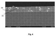
図4は、例1aに相当している、酸化ビスマスを含有しているガラス質バインダー20と気孔22とを含み散乱用粒子を添加していない本発明による散乱層の1000倍の倍率の断面傾斜SEM図を示している。
気孔は大きさがより小さく、表面はより滑らかである。粗さパラメーターRaは機械式の表面形状測定装置で測定され、200μmの分析長さにわたって、特に0.05μmきざみの測定で、Ra=30nmが得られる。FIG. 4 corresponds to Example 1a, a cross-sectional inclination at a magnification of 1000 times that of a scattering layer according to the invention comprising a
The pores are smaller in size and the surface is smoother. The roughness parameter Ra is measured with a mechanical surface profile measuring device, and Ra = 30 nm is obtained over an analysis length of 200 μm, especially in steps of 0.05 μm.
〔製造〕
耐薬品性を強化した散乱層の製造は、様々な工業的方法により、好ましくはスクリーン印刷によって、行うことができる。[Manufacturing]
The scattering layer with enhanced chemical resistance can be produced by various industrial methods, preferably by screen printing.
(ペースト)
スクリーン印刷用のペーストは、粒子に塗布スクリーンを通過させるためのキャリアとして働く、10%と50%の間の重量比率のスクリーン印刷用媒体からなる。(paste)
The screen printing paste consists of a screen printing medium in a weight ratio between 10% and 50% which serves as a carrier for the particles to pass through the application screen.
この媒体は、焼成シリカなどの微細な無機粒子あるいはセルロースエーテルと一緒にされてペーストに限界流動特性を与えるアルコール、グリコール、エステル又はテルピネオールからなる有機の媒体でよい。
有機媒体の燃焼によって気孔が生じる。This medium may be an organic medium composed of alcohol, glycol, ester or terpineol that is combined with fine inorganic particles such as calcined silica or cellulose ether to give the paste a limiting flow property.
Pores are generated by the combustion of the organic medium.
使用するペーストは、例えば、Ferro社により市販される媒体80840などのグリコールの混合物から構成される標準的なスクリーン印刷用媒体にガラスフリットを分散させて調製される。 The paste used is prepared, for example, by dispersing glass frit in a standard screen printing medium composed of a mixture of glycols such as medium 80840 marketed by Ferro.
ペーストをスクリーン印刷により使用するためのレオロジー特性を、焼成シリカ又はセルロースエーテルを使って最適化する。 The rheological properties for using the paste by screen printing are optimized using calcined silica or cellulose ether.
固形分(ガラス質バインダーを構成する)は、層に耐薬品性を与える先に示した高い比率の酸化ビスマスを含むガラスフリットである。 The solid (which constitutes the glassy binder) is a glass frit containing a high proportion of bismuth oxide as indicated above that gives the layer chemical resistance.
構成成分のペースト化は、遊星型ミキサーとディスクディスパーサーでもって高速度で行う。高速作業の前であれ後であれ、低速度の装置を併せて使用することもできる。これらの低速装置は、ニーダー又はビータータイプの攪拌機、あるいは毎分数回転の低速で動かされるローラーミキサーに数時間の間載置されるビーズを収容したフラスコからなる。ペーストの品質は、ヘグマンゲージを使って粒子又は凝集体が存在しないことにより評価される。 The components are pasted at high speed with a planetary mixer and a disk disperser. It is also possible to use a low-speed device together before or after high-speed work. These low speed devices consist of a kneader or beater type stirrer, or a flask containing beads that are placed for several hours in a roller mixer driven at a low speed of several revolutions per minute. The quality of the paste is assessed by the absence of particles or aggregates using a Hegman gauge.
(被着)
被着装置は、縮小した構成の電子タイプのもの(EKRA、DEK)でもよく、例えば板ガラス用などの工業規模のもの(THIEME)でもよい。
スクリーンは、布帛(例えばポリエステル)又は金属の網からなる。
マスクは、感光性レジスト又は金属板からなることができる。(Deposition)
The deposition apparatus may be an electronic type (EKRA, DEK) having a reduced configuration, and may be an industrial scale (THIEME) such as for sheet glass.
The screen is made of a fabric (for example, polyester) or a metal net.
The mask can be made of a photosensitive resist or a metal plate.
コーティングツールとドクターターブレードは、ポリマー、カーボン又は金属製である。ガラス基材上に被着する厚さは10μmと100μmの間である。厚さは、まず第一に、スクリーンのメッシュ及びその張力の選定によって制御される。
厚さはまた、スクリーンと基材との間隔の調整そしてまたブレードに加えられる圧力と移動の速度の調整によっても制御される。厚さは、被覆領域と非被覆領域との間でRodenstockタイプのレーザー光学ベンチを使って制御される。The coating tool and doctor blade are made of polymer, carbon or metal. The thickness deposited on the glass substrate is between 10 and 100 μm. The thickness is controlled primarily by the selection of the screen mesh and its tension.
The thickness is also controlled by adjusting the spacing between the screen and the substrate and also by adjusting the pressure applied to the blade and the speed of movement. The thickness is controlled using a Rodenstock type laser optical bench between the coated and uncoated areas.
被着物は、使用した媒体の特性に応じて、赤外線又は紫外線トンネル中で100〜150℃程度の温度で乾燥させる。 The adherend is dried at a temperature of about 100 to 150 ° C. in an infrared or ultraviolet tunnel depending on the characteristics of the medium used.
散乱層の被着は、スクリーン印刷以外の方法で、例えばロール塗布、浸漬塗布、ナイフ塗布、スプレー塗布、スピン塗布、あるいは流し塗布によって、行ってもよい。 The scattering layer may be applied by a method other than screen printing, for example, roll coating, dip coating, knife coating, spray coating, spin coating, or flow coating.
組成物のレオロジーを選定した被着方法に適応させるのに、粉体−液比の変更及び添加剤の使用を利用する。同様であるか、あるいは異なる組成を有するか、あるいは1以上の成分の勾配を有する層の積重体を作るために、2つの異なる被着方法を連続して使用してもよい。 To adapt the rheology of the composition to the selected deposition method, changes in the powder-liquid ratio and the use of additives are utilized. Two different deposition methods may be used in succession to create a stack of layers that are similar, have different compositions, or have a gradient of one or more components.
(焼成)
使用する炉は、自動車の後部窓ガラスの焼成用などのようなローラーにより搬送する、動的な炉でもよく、あるいは好ましくは、基材の平坦性を維持するため金属又はガラス−セラミックプレート上に配置する、静的な炉でもよい。焼成温度は580℃よりも高い。(Baking)
The furnace used may be a dynamic furnace, conveyed by rollers such as for the firing of rear windows of automobiles, or preferably on a metal or glass-ceramic plate to maintain the flatness of the substrate. A static furnace may be used. The firing temperature is higher than 580 ° C.
(クリーニングに対する耐性)
電子産業部門では、クリーンルームにおいて、まず第一に浴での手作業による又は自動化されたクリーニング処理に耐えなくてはならない層を含むこともあり含まないこともある基材を、普通に使用する。これらのクリーニング処理は基材から、いずれの微量の有機又は無機物質も、そしてまた粒子も、取り除かなくてはならない。従って、基材は、塩基性及び酸性の洗浄剤溶液と接触し、中間のすすぎ液と接触して、次々に各工程を通過する。クリーニング能力は、洗浄剤、超音波の存在により、そして多くの場合40℃に近い温度で、高められる。(Resistance to cleaning)
In the electronics industry, substrates are commonly used in clean rooms, first and foremost, which may or may not include layers that must withstand manual bathing or automated cleaning processes. These cleaning processes must remove any traces of organic or inorganic substances and also particles from the substrate. Thus, the substrate contacts the basic and acidic detergent solutions, contacts the intermediate rinse, and passes through each step in turn. The cleaning ability is enhanced by the presence of cleaning agents, ultrasound, and often at temperatures close to 40 ° C.
本発明によるガラス質散乱層の酸化ビスマスに富んだ組成は、前述の浴などのようなこれらの攻撃的な媒体中での耐性をそれに与える。同じ製造方法により製造した比較例のガラス質層は、同じクリーニング条件下で完全に破壊される。 The bismuth oxide rich composition of the glassy scattering layer according to the present invention gives it resistance in these aggressive media such as the baths described above. The comparative glassy layer produced by the same production method is completely destroyed under the same cleaning conditions.
〔OLEDの性能〕
本発明の散乱層の役割を説明するために、
・別の散乱層を加えずに(例REF 1、及びREF 1aとREF 1b)、
・酸化ビスマスなしの散乱層を加えながら(例REF 2、REF 2a及びREF 2b)、あるいは、
・例1の散乱層を加えながら(例A1、A1a、A1b)、
第2の面に結合したプラスチックの散乱フィルムを取り除いた第1、第2及び第3の商業的に入手できる有機発光ダイオードを使って、光の抽出と比色分析値の変動とについて測定を行った。[Performance of OLED]
In order to explain the role of the scattering layer of the present invention,
Without adding another scattering layer (eg
While adding a scattering layer without bismuth oxide (eg
While adding the scattering layer of Example 1 (Examples A1, A1a, A1b)
Measurements were made of light extraction and colorimetric variation using first, second and third commercially available organic light emitting diodes with the plastic scattering film bonded to the second surface removed. It was.
従って、例えば例REF 1、REF 2及びA1では、OSRAM社により市販されており白色光を与える、Orbeos(商標)として知られる照明用の第1の有機発光ダイオードを使用する。
例REF 1a、REF 2a及びA1aの場合は、LUMIOTEC社により市販されており白色光を与える、Lumiotec(商標)として知られる照明用の第2の有機発光ダイオードを使用する。
例REF 1b、REF 2b及びA1bの場合は、PHILIPS社により市販されており白色光を与える、Lumiblade(商標)として知られる照明用の第3の有機発光ダイオードを使用する。Thus, for example,
In the case of the examples REF 1a, REF 2a and A1a, a second organic light emitting diode for illumination, known as Lumiotec ™, which is commercially available from LUMIOTEC and gives white light is used.
In the case of the examples REF 1b, REF 2b and A1b, a third organic light-emitting diode for illumination known as Lumiblade ™, which is commercially available by PHILIPS and gives white light, is used.
最初に、抽出の増加が注目される。抽出の増加は、抽出された光の量の相対的な増加として定義され、すなわち、本発明の解決策(散乱層の追加)ありのデバイスとなしのデバイスにより放出される光の量の差と、解決策なしのデバイスによって放出される光の量との比として定義される。従って、それを測定するためには、解決策を施していないOLEDから出てゆく全光束と解決策を施したOLEDから出てゆくそれとを比較することが重要になる。両方の事例において光束の全部を確実に集めるために、2つのOLEDを公知のやり方でもって一つずつ、積分球内に配置する。 First, the increase in extraction is noted. The increase in extraction is defined as the relative increase in the amount of extracted light, i.e. the difference in the amount of light emitted by the device with and without the solution of the present invention (addition of a scattering layer). , Defined as the ratio to the amount of light emitted by the device without a solution. Therefore, in order to measure it, it is important to compare the total luminous flux emanating from the OLED without the solution and that emanating from the OLED with the solution. In order to reliably collect all of the luminous flux in both cases, two OLEDs are placed one by one in a known manner in an integrating sphere.
Orbeos(商標)とLumiblade(商標)の2つのOLEDについては、比較用の散乱層(REF 2及びREF 2b)を備えた例又は例1による散乱層(A1及びA1b)備えた例に関して、増加は実質的に40%であり、プラスチック散乱フィルムなしのダイオード(REF 1及びREF 1b)に関しては40%である。 For two OLEDs, Orbeos (TM) and Lumiblade (TM), the increase is relative to the example with the comparative scattering layer (
更に、Orbeos(商標)とLumiblade(商標)の2つのOLEDについては、散乱用粒子を含まない本発明による散乱層を備えた例の場合に増加は実質的に25%であり、プラスチック散乱フィルムなしのダイオード(REF 1及びREF 1b)に関しては25%である。 Furthermore, for the two OLEDs, Orbeos ™ and Lumiblade ™, the increase is substantially 25% in the case of the example with a scattering layer according to the invention which does not contain scattering particles, with no plastic scattering film For the other diodes (
最後に、下記の表4には前述の例REF 1〜A1bについての光路長Vc1〜Vc3を掲載している。Finally, Table 4 below lists the optical path lengths Vc1 to Vc3 for the
角度による比色分析値の変動は、散乱層ありの場合、特に本発明による散乱層ありの場合に、はるかに小さく、はるかにより均一な白色光を保証するということが認められる。 It can be seen that the variation in colorimetric values with angle is much smaller with a scattering layer, in particular with a scattering layer according to the invention, ensuring a much more uniform white light.
従って、基材上の本発明による散乱層は、OLEDの抽出の増加を増大させるのと、より均一な光を提供するため放出光の比色分析値の変動を減少させるのと、耐薬品性且つ耐熱性であることを、同時に可能にすることが分かる。 Thus, the scattering layer according to the present invention on the substrate increases the extraction of the OLED and reduces the variation in the colorimetric value of the emitted light to provide more uniform light, and is resistant to chemicals. It can also be seen that heat resistance is possible at the same time.
Claims (15)
Translated fromJapanese前記ガラス質のバインダー(20)が40〜60wt%の酸化ビスマスBi2O3、あるいは45〜58wt%の酸化ビスマスBi2O3を含むこと、
及び前記ガラス質バインダー(20)の比率が前記散乱層(2)の総重量の少なくとも20%であること、
を特徴とする有機発光ダイオードデバイスのための支持体。A transparent base material (10) made of inorganic glass having first and second opposing main surfaces (10a, 10b), a glassy inorganic binder (20) and a scattering structure dispersed in the binder A support for an organic light-emitting diode device (1) comprising a substrate (10) continuously coated on its second surface (10b) with a scattering layer (2) comprising elements (21, 22). And
The glassy binder (20) contains 40-60 wt% bismuth oxide Bi2 O3 , or 45-58 wt% bismuth oxide Bi2 O3 ;
And the ratio of the glassy binder (20) is at least 20% of the total weight of the scattering layer (2),
A support for an organic light-emitting diode device.
・0%〜10%、好ましくは0%〜5%のSiO2、
・0%〜5%、好ましくは0%〜1%のAl2O3、
・8%〜25%、好ましくは10%〜22%のB2O3、
・0%〜10%、好ましくは0%〜5%のCaO、
・0%〜20%、好ましくは0%〜15%のBaO、
・0%〜5%、好ましくは0%〜3%のLi2O、
・0%〜10%、好ましくは0%〜5%のNa2O、
・0%〜5%、好ましくは0%〜3%のK2O、
・0%〜5%、好ましくは0%〜4%のZrO2、
・0%〜5%のSrO、
・0%〜5%のLa2O3、
を含むことを特徴とする、請求項1又は2記載の支持体。The glassy binder (20) is wt%,
• 0% to 10%, preferably from 0% to 5% SiO2,
0% to 5%, preferably 0% to 1% Al2 O3 ,
8% to 25%, preferably 10% to 22% B2 O3 ,
0% to 10%, preferably 0% to 5% CaO,
0% to 20%, preferably 0% to 15% BaO,
0% to 5%, preferably 0% to 3% Li2 O,
0% to 10%, preferably 0% to 5% Na2 O,
0% to 5%, preferably 0% to 3% K2 O,
2.0% to 5%, preferably 0% to 4% of ZrO2,
0% to 5% SrO,
0% to 5% La2 O3 ,
The support according to claim 1 or 2, characterized by comprising:
及び/又は前記基材の第2面上に散乱層、酸化ビスマスなしのガラス質バインダーによって区別される層、を備えた第2の参照有機発光ダイオードデバイスについて、第3の経路長Vc3が同じようにして定義され、0.9以下、あるいは0.7以下のVc1/Vc3が得られ、好ましくはVc3は10-1以下であることを特徴とする、請求項14記載の有機発光ダイオードデバイス。In the CIE XYZ 1931 chromaticity diagram, emitting as output the spectrum of polychromatic light, especially white light, defined by chromaticity coordinates every 5 ° between the emission spectrum at 0 ° and the emission spectrum at 75 °; The path length Vc1 passing through an intermediate angle of 5 ° between the emission spectrum at 0 ° and the emission spectrum at 75 ° isexpressed by the following equation:
And / or for the second reference organic light emitting diode device comprising a scattering layer on the second surface of the substrate, a layer distinguished by a vitreous binder without bismuth oxide, the third path length Vc3 is the same15. An organic light emitting device according to claim 14, characterized in that a Vc1 / Vc3 of 0.9 or less or 0.7 or less is obtained, preferably Vc3 is 10−1 or less. Diode device.
Applications Claiming Priority (3)
| Application Number | Priority Date | Filing Date | Title |
|---|---|---|---|
| FR1056499AFR2963705B1 (en) | 2010-08-06 | 2010-08-06 | DIFFUSING LAYER HOLDER FOR ORGANIC ELECTROLUMINESCENT DIODE DEVICE, ORGANIC ELECTROLUMINESCENT DEVICE COMPRISING SUCH A SUPPORT |
| FR1056499 | 2010-08-06 | ||
| PCT/FR2011/051874WO2012017183A1 (en) | 2010-08-06 | 2011-08-05 | Support having a scattering layer for an organic light-emitting diode device, organic light-emitting device comprising such a support |
Publications (1)
| Publication Number | Publication Date |
|---|---|
| JP2013536551Atrue JP2013536551A (en) | 2013-09-19 |
Family
ID=43640173
Family Applications (1)
| Application Number | Title | Priority Date | Filing Date |
|---|---|---|---|
| JP2013523653APendingJP2013536551A (en) | 2010-08-06 | 2011-08-05 | Support having scattering layer for organic light emitting diode device, organic light emitting device including the support |
Country Status (7)
| Country | Link |
|---|---|
| US (1) | US8890133B2 (en) |
| EP (1) | EP2601695A1 (en) |
| JP (1) | JP2013536551A (en) |
| KR (1) | KR20130097744A (en) |
| CN (1) | CN103081158A (en) |
| FR (1) | FR2963705B1 (en) |
| WO (1) | WO2012017183A1 (en) |
Families Citing this family (23)
| Publication number | Priority date | Publication date | Assignee | Title |
|---|---|---|---|---|
| EP2767518A4 (en)* | 2011-10-14 | 2016-01-06 | Asahi Glass Co Ltd | GLASS FOR USE IN A DIFFUSION LAYER OF AN ORGANIC LIGHT-EMITTING DIODE (LED) ELEMENT, A MULTILAYER SUBSTRATE FOR USE IN AN ORGANIC LED ELEMENT AND METHOD FOR MANUFACTURING SAME, AND ORGANIC LED ELEMENT AND METHOD FOR MANUFACTURING THE SAME |
| DE102012206955B4 (en) | 2012-04-26 | 2016-09-22 | Osram Oled Gmbh | Method for producing a scattering layer for electromagnetic radiation |
| DE102012206967B4 (en)* | 2012-04-26 | 2025-04-10 | Pictiva Displays International Limited | Optoelectronic component and method for producing an optoelectronic component |
| CN103378265A (en)* | 2012-04-28 | 2013-10-30 | 展晶科技(深圳)有限公司 | Manufacturing method of light-emitting module carrier board |
| KR101715112B1 (en)* | 2012-06-14 | 2017-03-10 | 쌩-고벵 글래스 프랑스 | Layered body for OLED, method for manufacturing the same and OLED element having the same |
| US9921661B2 (en) | 2012-10-14 | 2018-03-20 | Neonode Inc. | Optical proximity sensor and associated user interface |
| US10282034B2 (en) | 2012-10-14 | 2019-05-07 | Neonode Inc. | Touch sensitive curved and flexible displays |
| US9164625B2 (en) | 2012-10-14 | 2015-10-20 | Neonode Inc. | Proximity sensor for determining two-dimensional coordinates of a proximal object |
| US10585530B2 (en) | 2014-09-23 | 2020-03-10 | Neonode Inc. | Optical proximity sensor |
| US9741184B2 (en) | 2012-10-14 | 2017-08-22 | Neonode Inc. | Door handle with optical proximity sensors |
| US10324565B2 (en) | 2013-05-30 | 2019-06-18 | Neonode Inc. | Optical proximity sensor |
| FR3002533A1 (en)* | 2013-02-25 | 2014-08-29 | Saint Gobain | SUBSTRATE FOR ORGANIC ELECTROLUMINESCENT DIODE DEVICE |
| US10084144B2 (en) | 2013-02-25 | 2018-09-25 | Saint-Gobain Glass France | Substrate for device having an organic light-emitting diode |
| ES2695052T3 (en)* | 2013-05-17 | 2018-12-28 | Saint-Gobain Glass France | OLED substrate transparent diffuser and method to produce such substrate |
| ES2693105T3 (en)* | 2013-05-17 | 2018-12-07 | Saint-Gobain Glass France | Transparent diffusive OLED substrate and method to produce such a substrate |
| CN105324741B (en)* | 2013-05-30 | 2019-12-06 | 内奥诺德公司 | Optical proximity sensor |
| KR101493612B1 (en)* | 2013-10-08 | 2015-02-13 | 쌩-고벵 글래스 프랑스 | A laminate for a light emitting device and process for preparing thereof |
| FR3020179B1 (en)* | 2014-04-22 | 2017-10-06 | Saint Gobain | ELECTRODE SUPPORTED TRANSPARENT FOR OLED |
| DE102014107099B4 (en) | 2014-05-20 | 2019-10-31 | Fraunhofer-Gesellschaft zur Förderung der angewandten Forschung e.V. | Light-scattering layer system, method for its production and use of the layer system |
| DE102017127624A1 (en) | 2017-11-22 | 2019-05-23 | Schott Ag | Coated glass or glass-ceramic substrate, coating comprising closed pores and method for coating a substrate |
| KR102103516B1 (en)* | 2018-08-29 | 2020-04-23 | 주식회사 첨단랩 | Structure for extracting light and organic electroluminescent lighting device |
| KR102797047B1 (en) | 2019-12-31 | 2025-04-21 | 네오노드, 인크. | Non-contact touch input system |
| GB202216380D0 (en)* | 2022-11-03 | 2022-12-21 | Pilkington Group Ltd | Luminescent coated substrate |
Citations (4)
| Publication number | Priority date | Publication date | Assignee | Title |
|---|---|---|---|---|
| US5326591A (en)* | 1992-10-19 | 1994-07-05 | Ferro Corporation | Bismuth-containing lead-free glass enamels and glazes of low silica content |
| JP2009238694A (en)* | 2008-03-28 | 2009-10-15 | Sumitomo Chemical Co Ltd | Organic electroluminescent element and its manufacturing method |
| FR2937467A1 (en)* | 2008-10-21 | 2010-04-23 | Saint Gobain | Organic LED device for use in e.g. display unit, has glass substrate with diffusing and absorbing layer containing particles dispersed in mineral binder, where proportions of binder and particles are specific percentages of weight of layer |
| WO2010084922A1 (en)* | 2009-01-26 | 2010-07-29 | 旭硝子株式会社 | Glass for scattering layer of organic led device and organic led device |
Family Cites Families (4)
| Publication number | Priority date | Publication date | Assignee | Title |
|---|---|---|---|---|
| CN101516794A (en)* | 2006-09-14 | 2009-08-26 | 旭硝子株式会社 | Optical glass and lens using the same |
| EP2278852A4 (en)* | 2008-03-18 | 2011-08-03 | Asahi Glass Co Ltd | ELECTRONIC DEVICE SUBSTRATE, LAYERED BODY FOR ORGANIC ELECTROLUMINESCENT DIODE ELEMENT, MANUFACTURING METHOD THEREOF, ORGANIC ELECTROLUMINESCENT DIODE ELEMENT, AND MANUFACTURING METHOD THEREOF |
| JP2010170969A (en)* | 2009-01-26 | 2010-08-05 | Asahi Glass Co Ltd | Substrate electrode and method of manufacturing the same, and organic led element and method of manufacturing the same |
| KR101653431B1 (en)* | 2009-01-26 | 2016-09-01 | 아사히 가라스 가부시키가이샤 | Glass composition and member having the same on substrate |
- 2010
- 2010-08-06FRFR1056499Apatent/FR2963705B1/ennot_activeExpired - Fee Related
- 2011
- 2011-08-05EPEP11757383.2Apatent/EP2601695A1/ennot_activeWithdrawn
- 2011-08-05USUS13/814,428patent/US8890133B2/ennot_activeExpired - Fee Related
- 2011-08-05JPJP2013523653Apatent/JP2013536551A/enactivePending
- 2011-08-05WOPCT/FR2011/051874patent/WO2012017183A1/enactiveApplication Filing
- 2011-08-05KRKR20137005652Apatent/KR20130097744A/ennot_activeWithdrawn
- 2011-08-05CNCN2011800422718Apatent/CN103081158A/enactivePending
Patent Citations (4)
| Publication number | Priority date | Publication date | Assignee | Title |
|---|---|---|---|---|
| US5326591A (en)* | 1992-10-19 | 1994-07-05 | Ferro Corporation | Bismuth-containing lead-free glass enamels and glazes of low silica content |
| JP2009238694A (en)* | 2008-03-28 | 2009-10-15 | Sumitomo Chemical Co Ltd | Organic electroluminescent element and its manufacturing method |
| FR2937467A1 (en)* | 2008-10-21 | 2010-04-23 | Saint Gobain | Organic LED device for use in e.g. display unit, has glass substrate with diffusing and absorbing layer containing particles dispersed in mineral binder, where proportions of binder and particles are specific percentages of weight of layer |
| WO2010084922A1 (en)* | 2009-01-26 | 2010-07-29 | 旭硝子株式会社 | Glass for scattering layer of organic led device and organic led device |
Also Published As
| Publication number | Publication date |
|---|---|
| WO2012017183A1 (en) | 2012-02-09 |
| CN103081158A (en) | 2013-05-01 |
| FR2963705B1 (en) | 2012-08-17 |
| FR2963705A1 (en) | 2012-02-10 |
| US8890133B2 (en) | 2014-11-18 |
| EP2601695A1 (en) | 2013-06-12 |
| KR20130097744A (en) | 2013-09-03 |
| US20130221336A1 (en) | 2013-08-29 |
Similar Documents
| Publication | Publication Date | Title |
|---|---|---|
| JP2013536551A (en) | Support having scattering layer for organic light emitting diode device, organic light emitting device including the support | |
| JP6073683B2 (en) | Glass substrate coated with high refractive index layer under electrode coating and organic light emitting device comprising the substrate | |
| CN101766052B (en) | Translucent substrate, method for manufacturing the translucent substrate, organic led element and method for manufacturing the organic LED element | |
| EP2384086B1 (en) | Substrate for electronic device and electronic device using same | |
| US7884547B2 (en) | Lead-free acid-resistant glass composition and glass paste comprised of the same | |
| JP6114395B2 (en) | Production method of transparent diffusion OLED substrate and obtained substrate | |
| JP2009126782A (en) | Low melting point frit paste composition and electrical element sealing method using the same | |
| JP7375762B2 (en) | Glass substrate, black matrix substrate and display panel | |
| JP6117995B2 (en) | Transparent scattering OLED substrate and method for producing the substrate | |
| JP6495894B2 (en) | Transparent diffusive OLED substrate and method for producing the substrate | |
| JP6608932B2 (en) | Transparent diffusive OLED substrate and method for producing the substrate | |
| JP2007302510A (en) | Glass paste composition and partition wall for display device using the same | |
| RU2656261C2 (en) | Transparent diffusive oled substrate and method for producing such substrate | |
| WO2014010621A1 (en) | Light extraction layer forming glass, and light extraction layer forming glass powder, method for forming light extraction layer, material for forming light extraction layer, glass paste for forming light extraction layer, glass substrate for organic el element, organic el element and method for manufacturing glass substrate for organic el element which use same | |
| JP6327579B2 (en) | Manufacturing method of glass substrate for organic EL element | |
| JP6278230B2 (en) | Glass substrate for organic EL device | |
| RU2070749C1 (en) | Method for manufacturing face glass plate of gaseous-discharge display panel | |
| JP2015071514A (en) | Glass for formation of light extraction layer, material for formation of light extraction layer, glass substrate provided with light extraction layer and organic el element using them |
Legal Events
| Date | Code | Title | Description |
|---|---|---|---|
| A621 | Written request for application examination | Free format text:JAPANESE INTERMEDIATE CODE: A621 Effective date:20140708 | |
| A977 | Report on retrieval | Free format text:JAPANESE INTERMEDIATE CODE: A971007 Effective date:20150316 | |
| A131 | Notification of reasons for refusal | Free format text:JAPANESE INTERMEDIATE CODE: A131 Effective date:20150324 | |
| A601 | Written request for extension of time | Free format text:JAPANESE INTERMEDIATE CODE: A601 Effective date:20150623 | |
| A02 | Decision of refusal | Free format text:JAPANESE INTERMEDIATE CODE: A02 Effective date:20151208 |