JP2013532587A - Grinding tool for trapezoidal grinding of wafers - Google Patents
Grinding tool for trapezoidal grinding of wafersDownload PDFInfo
- Publication number
- JP2013532587A JP2013532587AJP2013521270AJP2013521270AJP2013532587AJP 2013532587 AJP2013532587 AJP 2013532587AJP 2013521270 AJP2013521270 AJP 2013521270AJP 2013521270 AJP2013521270 AJP 2013521270AJP 2013532587 AJP2013532587 AJP 2013532587A
- Authority
- JP
- Japan
- Prior art keywords
- wafer
- grinding
- groove
- grooves
- wheel
- Prior art date
- Legal status (The legal status is an assumption and is not a legal conclusion. Google has not performed a legal analysis and makes no representation as to the accuracy of the status listed.)
- Withdrawn
Links
- 238000000227grindingMethods0.000titleclaimsabstractdescription122
- 235000012431wafersNutrition0.000titledescription128
- 230000002093peripheral effectEffects0.000claimsdescription19
- 229910003460diamondInorganic materials0.000claimsdescription8
- 239000010432diamondSubstances0.000claimsdescription8
- 238000000034methodMethods0.000description37
- 239000000758substrateSubstances0.000description23
- 230000008569processEffects0.000description17
- XUIMIQQOPSSXEZ-UHFFFAOYSA-NSiliconChemical compound[Si]XUIMIQQOPSSXEZ-UHFFFAOYSA-N0.000description7
- 238000004519manufacturing processMethods0.000description7
- 229910052710siliconInorganic materials0.000description7
- 239000010703siliconSubstances0.000description7
- 239000012212insulatorSubstances0.000description6
- 238000005498polishingMethods0.000description6
- 239000000463materialSubstances0.000description5
- 239000004065semiconductorSubstances0.000description5
- 230000032798delaminationEffects0.000description4
- 238000005530etchingMethods0.000description4
- 239000002245particleSubstances0.000description4
- 238000005304joiningMethods0.000description3
- JBRZTFJDHDCESZ-UHFFFAOYSA-NAsGaChemical compound[As]#[Ga]JBRZTFJDHDCESZ-UHFFFAOYSA-N0.000description2
- 229910001218Gallium arsenideInorganic materials0.000description2
- 238000011109contaminationMethods0.000description2
- 239000013078crystalSubstances0.000description2
- 229910052732germaniumInorganic materials0.000description2
- GNPVGFCGXDBREM-UHFFFAOYSA-Ngermanium atomChemical compound[Ge]GNPVGFCGXDBREM-UHFFFAOYSA-N0.000description2
- 238000010438heat treatmentMethods0.000description2
- 230000009467reductionEffects0.000description2
- 229910000838Al alloyInorganic materials0.000description1
- 241001050985DiscoSpecies0.000description1
- 229910002601GaNInorganic materials0.000description1
- JMASRVWKEDWRBT-UHFFFAOYSA-NGallium nitrideChemical compound[Ga]#NJMASRVWKEDWRBT-UHFFFAOYSA-N0.000description1
- 229910000577Silicon-germaniumInorganic materials0.000description1
- LEVVHYCKPQWKOP-UHFFFAOYSA-N[Si].[Ge]Chemical compound[Si].[Ge]LEVVHYCKPQWKOP-UHFFFAOYSA-N0.000description1
- 239000002253acidSubstances0.000description1
- 239000003513alkaliSubstances0.000description1
- 238000003486chemical etchingMethods0.000description1
- 238000004140cleaningMethods0.000description1
- PMHQVHHXPFUNSP-UHFFFAOYSA-Mcopper(1+);methylsulfanylmethane;bromideChemical compoundBr[Cu].CSCPMHQVHHXPFUNSP-UHFFFAOYSA-M0.000description1
- 238000005336crackingMethods0.000description1
- 230000007547defectEffects0.000description1
- 238000005259measurementMethods0.000description1
- 229910001092metal group alloyInorganic materials0.000description1
- 238000012986modificationMethods0.000description1
- 230000004048modificationEffects0.000description1
- 230000003647oxidationEffects0.000description1
- 238000007254oxidation reactionMethods0.000description1
- 238000004806packaging method and processMethods0.000description1
- 238000006722reduction reactionMethods0.000description1
- 229910052594sapphireInorganic materials0.000description1
- 239000010980sapphireSubstances0.000description1
- 238000007493shaping processMethods0.000description1
- 229910001220stainless steelInorganic materials0.000description1
- 239000010935stainless steelSubstances0.000description1
- 238000004381surface treatmentMethods0.000description1
- ISIJQEHRDSCQIU-UHFFFAOYSA-Ntert-butyl 2,7-diazaspiro[4.5]decane-7-carboxylateChemical compoundC1N(C(=O)OC(C)(C)C)CCCC11CNCC1ISIJQEHRDSCQIU-UHFFFAOYSA-N0.000description1
Images


Classifications
- B—PERFORMING OPERATIONS; TRANSPORTING
- B24—GRINDING; POLISHING
- B24B—MACHINES, DEVICES, OR PROCESSES FOR GRINDING OR POLISHING; DRESSING OR CONDITIONING OF ABRADING SURFACES; FEEDING OF GRINDING, POLISHING, OR LAPPING AGENTS
- B24B9/00—Machines or devices designed for grinding edges or bevels on work or for removing burrs; Accessories therefor
- B24B9/02—Machines or devices designed for grinding edges or bevels on work or for removing burrs; Accessories therefor characterised by a special design with respect to properties of materials specific to articles to be ground
- B24B9/06—Machines or devices designed for grinding edges or bevels on work or for removing burrs; Accessories therefor characterised by a special design with respect to properties of materials specific to articles to be ground of non-metallic inorganic material, e.g. stone, ceramics, porcelain
- B24B9/065—Machines or devices designed for grinding edges or bevels on work or for removing burrs; Accessories therefor characterised by a special design with respect to properties of materials specific to articles to be ground of non-metallic inorganic material, e.g. stone, ceramics, porcelain of thin, brittle parts, e.g. semiconductors, wafers
- B—PERFORMING OPERATIONS; TRANSPORTING
- B24—GRINDING; POLISHING
- B24D—TOOLS FOR GRINDING, BUFFING OR SHARPENING
- B24D5/00—Bonded abrasive wheels, or wheels with inserted abrasive blocks, designed for acting only by their periphery; Bushings or mountings therefor
- B24D5/14—Zonally-graded wheels; Composite wheels comprising different abrasives
Landscapes
- Engineering & Computer Science (AREA)
- Mechanical Engineering (AREA)
- Chemical & Material Sciences (AREA)
- Ceramic Engineering (AREA)
- Inorganic Chemistry (AREA)
- Mechanical Treatment Of Semiconductor (AREA)
- Polishing Bodies And Polishing Tools (AREA)
Abstract
Translated fromJapaneseDescription
Translated fromJapanese本開示は、シリコン・オン・インシュレータ(SOI)接合構造体等の半導体およびソーラウエハ(solar wafer)に関し、より具体的には、接合SOIウエハを研削するための研削工具に関する。 The present disclosure relates to semiconductors such as silicon-on-insulator (SOI) bonded structures and solar wafers, and more particularly to grinding tools for grinding bonded SOI wafers.
半導体ウエハは一般に、個別のウエハへとスライスされる単結晶インゴット(例えばシリコンインゴット)から製造される。本明細書において、シリコンで構成される半導体ウエハに言及しているが、ゲルマニウム、ヒ化ガリウムまたは後述の他の材料等の他の材料を同様に使用してよい。一の種類のウエハは、シリコン・オン・インシュレータ(SOI)ウエハである。SOIウエハは、絶縁体層(即ち酸化物層)の上にシリコンの薄層(活性層)を有し、その絶縁体層は、シリコン基板の上に配置される。接合SOI半導体ウエハはSOI構造体の一種である。 Semiconductor wafers are typically manufactured from single crystal ingots (eg, silicon ingots) that are sliced into individual wafers. Although reference is made herein to semiconductor wafers made of silicon, other materials such as germanium, gallium arsenide, or other materials described below may be used as well. One type of wafer is a silicon-on-insulator (SOI) wafer. An SOI wafer has a thin silicon layer (active layer) on an insulator layer (ie, an oxide layer), and the insulator layer is disposed on a silicon substrate. A bonded SOI semiconductor wafer is a kind of SOI structure.
電子産業におけるデバイス幅の縮小、電力の節約、超高速性能および/または特別な用途に起因して、SOI(シリコン・オン・インシュレータ)ウエハにおける要望が増大している。挑戦の1つとして、剥離を回避するために、支持基板に接合された活性層ウエハの、接合していない外側の周辺部を効果的に取り除くことが挙げられる。剥離は、ウエハの加工および/またはデバイスラインにおいて粒子の汚染を引き起こし得る。 Due to device width reduction, power savings, ultra-high speed performance and / or special applications in the electronics industry, there is an increasing demand for SOI (Silicon on Insulator) wafers. One challenge is to effectively remove the non-bonded outer periphery of the active layer wafer bonded to the support substrate to avoid delamination. Delamination can cause particle contamination in wafer processing and / or device lines.
SOIウエハを製造する際、接合すべき2つのウエハの外側の周辺部は、ウエハの破損、亀裂および/または粒子の発生を防ぐために、RもしくはT面取り又はエッジプロファイリング(以下に更に説明する)に付される。また、接合基板の外側の周辺部の厚さは、ウエハリング工程に起因して不均一である。この不均一な厚さを原因として、接合プロセスの間に、外側の周辺部が全く接合されず且つ/又は弱く接合される。活性ウエハの厚さを研削、エッチング、研磨等のプロセスにより小さくすると、この接合していない部分は、膜厚を小さくする工程の間に、接合基板から部分的に剥離する。剥離した部分は、膜厚の減少、洗浄および測定プロセスに対して問題を引き起こす。更に、デバイス加工において、残存する接合していない部分が剥離し、それにより、粒子が発生し、デバイスの収率に深刻な影響を及ぼす。 When manufacturing SOI wafers, the outer periphery of the two wafers to be bonded is R or T chamfered or edge profiling (described further below) to prevent wafer breakage, cracking and / or particle generation. Attached. Further, the thickness of the peripheral portion outside the bonded substrate is non-uniform due to the wafering process. Due to this uneven thickness, the outer periphery is not joined at all and / or weakly joined during the joining process. When the thickness of the active wafer is reduced by processes such as grinding, etching, and polishing, the unbonded portion is partially peeled from the bonded substrate during the step of reducing the film thickness. The delaminated areas cause problems for film thickness reduction, cleaning and measurement processes. Furthermore, in device processing, the remaining unbonded portions are peeled off, thereby generating particles and seriously affecting the device yield.
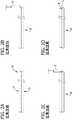
剥離を解決しようとするいくつかの従来技術が存在している。例えば、図1A〜1Dは、基板ウエハSと活性層ウエハAとを互いに接合し、次いで、接合ウエハWの縁部の周辺部を面取りする工程の連続を示している。図1Aは、活性層ウエハの下の基板を示しており、図1Bは接合ウエハを示している。図1Cは、ウエハの外側周縁部を研削する研削機(またはグラインダ)Gを示しており、図1Dは完成したSOIウエハWを示している(完成したウエハは更に加工されることに留意されたい)。この方法は、日本国特許出願第1986−256621号に示される方法と実質的に類似していると考えられる。この例の他の欠点の中には、ウエハWの直径が標準的なウエハ直径より小さいことがあり、それにより、下流の取扱設備および治具に関して問題が生じる。 There are several prior arts that attempt to resolve delamination. For example, FIGS. 1A to 1D show a series of steps of bonding the substrate wafer S and the active layer wafer A to each other and then chamfering the peripheral portion of the edge of the bonded wafer W. FIG. 1A shows the substrate under the active layer wafer, and FIG. 1B shows the bonded wafer. FIG. 1C shows a grinder (or grinder) G that grinds the outer peripheral edge of the wafer, and FIG. 1D shows the completed SOI wafer W (the completed wafer is further processed). ). This method is considered to be substantially similar to the method shown in Japanese Patent Application No. 1986-256621. Among other drawbacks of this example, the diameter of the wafer W may be smaller than the standard wafer diameter, which creates problems with downstream handling equipment and fixtures.
図2A〜2Dに示す別の従来技術の例において、接合SOIウエハWが、上述のように活性層ウエハAおよび基板ウエハSから形成される。ウエハの縁部は、図2B〜2Cに示すように、活性ウエハAの外縁部全体が削り落とされるが基板の一部のみが削り落とされるように研削される。この方法は、日本国特許出願第1989−227441号に示される方法と実質的に類似していると考えられる。この方法は、効率が悪くなってしまう。 In another prior art example shown in FIGS. 2A-2D, a bonded SOI wafer W is formed from an active layer wafer A and a substrate wafer S as described above. 2B to 2C, the edge portion of the wafer is ground so that the entire outer edge portion of the active wafer A is scraped off, but only a part of the substrate is scraped off. This method is considered to be substantially similar to the method shown in Japanese Patent Application No. 1989-227441. This method is inefficient.
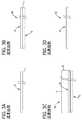
図3Aに示す従来技術の例において、活性ウエハAはその縁部が研削されて出っ張り(ledge)Lが形成される(従って、ウエハAは予め研削されたウエハである)。ウエハAは図3Bにおいて基板ウエハSに接合される。図3Cにおいて、接合SOIウエハWの上面が研削されて出っ張りLが除去され、完成したウエハが図3Dに示される。活性層ウエハの接合していない部分は、その後、削り落とされる。この方法は、日本国特許出願第1992−85827号に示される方法と実質的に類似していると考えられる。 In the prior art example shown in FIG. 3A, the edge of active wafer A is ground to form a ledge L (thus, wafer A is a pre-ground wafer). Wafer A is bonded to substrate wafer S in FIG. 3B. In FIG. 3C, the upper surface of the bonded SOI wafer W is ground to remove the protrusion L, and the completed wafer is shown in FIG. 3D. The unbonded portion of the active layer wafer is then scraped off. This method is considered to be substantially similar to the method shown in Japanese Patent Application No. 1992-85827.
図4Aの従来技術において、接合SOIウエハWは上述のように、活性層ウエハAおよび基板ウエハSから形成される。図4Bにおいて、活性ウエハAはその上部周縁部Eが研削されて図4Cに示す出っ張りLが形成される。図4Dのウエハ加工を完成させるために、選択的エッチング、研磨および/またはPAC(プラズマアシスト化学エッチング)法を用いて、活性層ウエハAの外側周縁部から接合していない部分を除去する。この方法は、米国特許第6,534,384号B2(参照することにより本明細書に組み込まれる)に示される方法と実質的に類似していると考えられる。以上のように、完成したウエハを形成するのに多数の工程が必要とされる。 4A, the bonded SOI wafer W is formed from the active layer wafer A and the substrate wafer S as described above. 4B, the upper peripheral edge E of the active wafer A is ground to form a ledge L shown in FIG. 4C. To complete the wafer processing of FIG. 4D, the non-bonded portion is removed from the outer peripheral edge of the active layer wafer A using selective etching, polishing and / or PAC (plasma assisted chemical etching) methods. This method is believed to be substantially similar to that shown in US Pat. No. 6,534,384 B2, which is incorporated herein by reference. As described above, a number of processes are required to form a completed wafer.
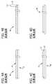
図5Aの従来技術において、活性層ウエハAは、接合に先立って、その下面において溝Rが形成されている。活性ウエハAは、図5Bにおいて基板ウエハSに接合される。この方法は、米国特許出願第2009/0203167号A1(参照することにより本明細書に組み込まれる)に示される方法と実質的に類似していると考えられる。図5Cにおいて、ウエハAの溝Rと反対側において研削を実施する。ウエハAの外側の周辺部の接合していない部分は、図5Dの完成したウエハWにおいて示すように、ウエハを所定の厚さに研削した後に取り除くことができる。 In the prior art of FIG. 5A, the active layer wafer A has a groove R formed on its lower surface prior to bonding. The active wafer A is bonded to the substrate wafer S in FIG. 5B. This method is believed to be substantially similar to that shown in US Patent Application No. 2009/0203167 A1 (incorporated herein by reference). In FIG. 5C, grinding is performed on the side opposite to the groove R of the wafer A. The unbonded portion of the outer periphery of wafer A can be removed after grinding the wafer to a predetermined thickness, as shown in the completed wafer W in FIG. 5D.
ウエハの表面処理方法に関して、および接合構造体の活性層の外側の周辺部の剥離を防ぐ現在の方法の不都合な点に対処するウエハに関して、満たされていない要求が残っている。 There remains an unmet need for wafer surface treatment methods and for wafers that address the disadvantages of current methods of preventing delamination of the outer periphery of the active layer of the bonded structure.
一の態様において、プロファイリング(または形状加工もしくは面取り)機械においてウエハを台形研削するための研削工具は、環状の車輪をスピンドルに取り付けるのに適用される中央の孔を有する環状の車輪(annular wheel)を含む。車輪は、車輪の外縁部に配置される少なくとも2つの溝を有し、溝は、ウエハの外縁部を受けるようなサイズである。溝の少なくとも1つはウエハの粗研削に適用される。少なくとも1つの他の溝はウエハの精密(または微細)研削に適用される。 In one aspect, a grinding tool for trapezoidally grinding a wafer in a profiling (or shaping or chamfering) machine includes an annular wheel having a central hole applied to attach the annular wheel to a spindle. including. The wheel has at least two grooves disposed at the outer edge of the wheel, the groove being sized to receive the outer edge of the wafer. At least one of the grooves is applied to rough grinding of the wafer. At least one other groove is applied for precision (or fine) grinding of the wafer.
もう一つの態様において、研削工具の車輪は、車輪の外縁部に配置される3つ以上の溝を有し、溝は、ウエハの外縁部を受けるようなサイズである。溝の少なくとも1つはウエハの粗研削に適用され、少なくとも1つの他の溝はウエハの精密研削に適用される。各溝は、ウエハの上部周縁部のみが研削されるようなサイズおよび形状である。 In another aspect, the wheel of the grinding tool has three or more grooves disposed on the outer edge of the wheel, the grooves being sized to receive the outer edge of the wafer. At least one of the grooves is applied to rough grinding of the wafer and at least one other groove is applied to precision grinding of the wafer. Each groove is sized and shaped so that only the upper peripheral edge of the wafer is ground.
更にもう一つの態様において、プロファイリング機械においてウエハを研削するための研削工具は、環状の車輪をスピンドルに取り付けるのに適用される中央の孔を有する環状の車輪を含む。車輪は、車輪の外縁部に配置される3つ以上の溝を有し、溝は、ウエハの外縁部を受けるようなサイズである。一の溝はウエハの粗研削のためのものであり、少なくとも2つの溝はウエハの精密研削のためのものである。各溝は、ウエハの上部周縁部のみが研削されるように、断面においてV字形を有し、かつウエハに対してサイズが決められる。 In yet another aspect, a grinding tool for grinding a wafer in a profiling machine includes an annular wheel having a central hole applied to attach the annular wheel to a spindle. The wheel has three or more grooves disposed at the outer edge of the wheel, the groove being sized to receive the outer edge of the wafer. One groove is for rough grinding of the wafer and at least two grooves are for precision grinding of the wafer. Each groove has a V-shape in cross section and is sized relative to the wafer so that only the upper peripheral edge of the wafer is ground.
上述の態様に関連して記載される特徴の種々の改良が存在する。更なる特徴もまた同様に、上述の態様に組み込まれてよい。これらの改良および追加の特徴は、個別に又は任意の組み合わせで存在してよい。例えば、例示されるいずれかの実施形態に関連して以下に論じる種々の特徴を、単独で又は任意の組み合わせで上述の態様のいずれにも組み込んでよい。 There are various improvements to the features described in connection with the above-described aspects. Additional features may also be incorporated into the embodiments described above as well. These refinements and additional features may exist individually or in any combination. For example, the various features discussed below in connection with any illustrated embodiment may be incorporated into any of the above aspects, either alone or in any combination.
図面は縮尺通りではなく、例示を目的として一部が拡大されている。対応する参照文字は図面全体にわたって対応する部材を表している。 The drawings are not to scale and are partially enlarged for illustrative purposes. Corresponding reference characters indicate corresponding parts throughout the drawings.
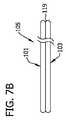
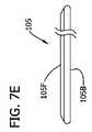
ここで、図6および7A〜7Eを参照して、接合ウエハ(あるいは、シリコン・オン・インシュレータ構造体またはSOIウエハ)を製造または加工する方法100を示す。図7Aに示すような活性ウエハ101および基板ウエハ103は常套的なウエハである。両者は鏡面研磨された前面101F、103Fを有し、比較的欠陥がない。 6 and 7A-7E, a
活性ウエハ101および基板ウエハ103は、SOI構造体において使用するのに適した任意の単結晶半導体材料であってよい。一般に、ウエハは、シリコン、ゲルマニウム、ヒ化ガリウム、シリコンゲルマニウム、窒化ガリウム、窒化アルミニウム、亜リン酸、サファイアおよびこれらの組み合わせからなる群から選択される材料で構成されてよい。一の実施形態において、ウエハ101、103はシリコンから作製される。 The
酸化物の層を活性ウエハの前面に堆積させる(102)。酸化は通常、垂直炉、例えば市販されているAMS400において実施する。次いで、ウエハの前面を、基板ウエハの前面に接合して(104)、図7Bに示すように接合ウエハ105を形成する。接合は、オーストリアのEV Group製のModel EVG(登録商標)850等のツールを用いて、常套的な親水性接合プロセスにおいて実施することができる。電気炉(ペンシルバニアのTPS製のモデルBlue M等)において熱処理106を適切に実施して接合を強化する。次の工程、台形研削108を、図7Cを参照して以下に更に説明する。図7Cに示す平面研削110は、日本のDisco Corporation製のモデルDFG−830等の片面研削機を用いて適切に実施される。平面研削110は、粗研削工程および精密研削工程を適切に含む。粗研削は、20〜30ミクロンのグリットサイズの600メッシュを用いて適切に実施され、精密研削は3000メッシュおよび2〜6ミクロンのグリットサイズで実施される。 An oxide layer is deposited on the front side of the active wafer (102). Oxidation is typically carried out in a vertical furnace, such as the commercially available AMS 400. Next, the front surface of the wafer is bonded to the front surface of the substrate wafer (104) to form a bonded
次に、再び図6を参照して、接合ウエハ105においてエッチング112を実施し、常套的なエッチング装置においてアルカリエッチャントを用いて適切に実施するが、酸エッチャントを用いてもよい。次いで、研磨114を実施し、Strasbaugh Mark 9−Kを用いて、前面105Fにおける片面研磨を適切に実施する。別法として、研磨114は、前面105Fおよび裏面105Bの両方の両面研磨をであってよい。接合ウエハ105の仕上げ116は、平面度および粒子数等の必要とされる全てのパラメータに関してウエハを検査することと、次いで、顧客に出荷するためにウエハをパッケージングすることとを含む。 Next, referring to FIG. 6 again, the
図7Eおよび13からわかるように、仕上げられた又は接合されたウエハ105は台形形状を有する上部を有する。より具体的には、活性層ウエハ101の残余と、基板ウエハの比較的小さい部分とを含む上部は、外側周縁部において角を有しており、その結果、ウエハは、台形形状を有している又は断面において台形形状を有していると考えられる。接合ウエハ105の下部(この実施形態における基板ウエハ103に実質的に対応している)は、その外側周縁部において常套的な傾斜した形状または丸みを帯びた形状(概して湾曲した形状)を有し、従って、台形形状を有しないことに留意されたい。この実施形態において、接合ウエハ105の上部は、活性ウエハ101と実質的に一致する。 As can be seen from FIGS. 7E and 13, the finished or bonded
再び図7Cを参照して、活性ウエハ101の外側周縁部を研石車に接触させ、接合ウエハ105の前面105Fに対して斜めに研削する。角度は、適切には約3°〜10°であり、この実施形態において、角度は約7°である。外側周縁部全体が図7Dに示すように研削されるまで、エッジ研削を実施する。研削は、外側周縁部におけるいずれのノッチも除去する。研削は、角度付けられた又は傾斜した部分の長さが約1mm〜1.5mm、例えば約1.25mmであるように適切に行ってよい。研削の角度および深さは、基板ウエハ103の上部傾斜119のごく一部が台形研削の間に除去されるようなものであることに留意されたい。 Referring to FIG. 7C again, the outer peripheral edge of the
図7Cにおいて、活性ウエハ101の表面を、図7Dに示すように厚さが40〜50ミクロンになるまで研削する。図7Dにおける活性ウエハ101の台形形状に留意されたい。また、基板ウエハ103の一部が研削されるように、エッジ研削を実施する。 In FIG. 7C, the surface of the
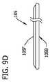
図8および9A〜9Dを参照して、図6および7A〜7Dの研削工程と比較して研削工程を逆転させる。換言すれば、台形研削の前に、活性ウエハ101の表面を先ず研削する。この工程の順番を図8に示す。この場合も同様に、平面研削工程は、粗研削工程および精密研削工程を含んでよい。粗研削は、600メッシュおよび20〜30ミクロンのグリットサイズを用いて適切に実施し、精密研削は、3000メッシュおよび2〜6ミクロンのグリットサイズで実施する。表面は、図9Bに示すように研削し、そして次に、図9Cにおいて、活性ウエハ101の縁部を、縁部が図9Dに示す台形形状を有するまで研削する。 With reference to FIGS. 8 and 9A-9D, the grinding process is reversed as compared to the grinding process of FIGS. 6 and 7A-7D. In other words, the surface of the
図10および11を参照して、一の実施形態の砥石車151(概して台形研削工具)を、台形研削108の実施のために設計する。砥石車151は、台形研削を実施する常套的なエッジプロファイリング機械152に取り付けられるようになっている。この実施形態において、プロファイリング機械は直径200mmのウエハに適合するSTC EP−5800RHO機である。砥石車151はプロファイリング機械152のスピンドル(または軸z)153に取り付けられる。 With reference to FIGS. 10 and 11, one embodiment of a grinding wheel 151 (generally a trapezoidal grinding tool) is designed for performing trapezoidal grinding 108. The
この実施形態の砥石車151は、輪状または環状であり、プロファイリング機械152のスピンドル151に砥石車を取り付けるのに適用される中央の孔154を有する。砥石車151は202mmの直径Dを有し、中央の孔の直径HDは30mmであり、厚さは20mmである。この実施形態の砥石車151は、砥石車の外縁部に配置される上部の溝155、中央の溝157および下部の溝159を有する。この実施形態において、溝155、157、159は概してV字型である。別法として、砥石車151は、本開示の範囲内において、ただ1つの溝を有してよく、または実用的には任意の他の数の溝を有してよいことに留意されたい。 The
この実施形態において、上部の溝155および中央の溝157は精密研削に適用され、下部の溝159は粗研削に適用される。各溝は、ダイアモンドグリットを適切に含む。精密研削に関しては、2000または3000メッシュのダイアモンドグリットサイズが好適である。粗研削に関しては、600メッシュまたは800メッシュが好適である。砥石車151は金属合金、アルミニウム合金またはステンレス鋼から適切に作製されるが、他の材料も考えられる。 In this embodiment, the
この実施形態の各溝壁は、溝の底部から溝の頂部へと傾斜しており、平坦な底部を有する。この実施形態において、傾斜は約7°の角度である。溝の底部の幅は、約200mmの総厚さを有する接合ウエハに使用する場合には約1.8mmであり、その結果、基板ウエハまたはウエハの裏面は台形研削の間、溝に接触しない。各溝の、最も幅が広い部分(溝の頂部)における幅は約3.5mmである。溝の壁は、約0.2mmの半径で、溝の底部へと湾曲している。溝の深さGDは約6.0mmであり、溝の根本(root)の深さRDは約8.0mmである。 Each groove wall in this embodiment is inclined from the bottom of the groove to the top of the groove and has a flat bottom. In this embodiment, the slope is an angle of about 7 °. The width of the bottom of the groove is about 1.8 mm when used on a bonded wafer having a total thickness of about 200 mm, so that the substrate wafer or backside of the wafer does not contact the groove during trapezoidal grinding. The width of each groove at the widest portion (the top of the groove) is about 3.5 mm. The groove wall is curved to the bottom of the groove with a radius of about 0.2 mm. The depth GD of the groove is about 6.0 mm, and the depth RD of the root of the groove is about 8.0 mm.
砥石車151は、エッジプロファイリング機械152(STC EP−5800 RHOのスピンドル等)に設置される。砥石車を設置した後、スピンドル高さ(垂直方向)および距離(水平方向)を微調整し、その結果、砥石車151の溝155と接合ウエハ105とが、図12に示すように位置決めされる。基板ウエハの縁部の最外部および底面が研削溝155に接触していないことに留意されたい。次いで、台形研削を上述のように実施する。台形研削は、粗いグリット溝もしくは精密なグリット溝のいずれか、または両方のグリット溝(まず粗いグリット溝、次いで精密なグリット溝)を用いて実施することができる。研削は、例えばエッジの品質の要求に応じて、シングルパス(または単一の工程)またはマルチパス(または複数の工程)として実施してよい。 The
上述の例の方法は、基板ウエハに接合される活性層ウエハの、接合されていない外側の周辺部を取り除くのに適用される。これにより、よりしっかりと接合された外側の周辺部を有する接合ウエハがもたらされる。適切な方法において、支持基板の上に活性層ウエハを接合し、接合対の接合後の熱処理を行った後に、台形研削を適用して活性層ウエハの接合していない外側の周辺部を取り除く。砥石車151等のエッジ砥石車を用いて台形研削工程を実施してよい。他の利点の中に、本開示の実施形態による接合ウエハは、剥離してしまう可能性が低いことがある。更に、接合ウエハは、さもなければウエハの加工/デバイスラインにおける接合していない部分の剥離に起因して生じることがある粒子汚染を妨げ、または防止する。 The example method described above is applied to remove the unbonded outer periphery of the active layer wafer that is bonded to the substrate wafer. This results in a bonded wafer having an outer periphery that is more firmly bonded. In an appropriate method, the active layer wafer is bonded onto the support substrate, and after the heat treatment after bonding of the bonded pair, trapezoidal grinding is applied to remove the non-bonded outer periphery of the active layer wafer. The trapezoidal grinding process may be performed using an edge grinding wheel such as a
本発明または本発明の(1以上の)実施形態の構成要素を導入する際、冠詞「a」、「an」、「the」および「said」は、その構成要素が1以上存在することを意味することが意図される。用語「含む」、「含有する」および「有する」は、包含的であることが意図され、列挙された構成要素の他に追加の構成要素が存在してよいことを意味することが意図される。 In introducing a component of the present invention or one or more embodiments of the present invention, the articles “a”, “an”, “the” and “said” mean that there is one or more of the component. Is intended to be. The terms “comprising”, “containing” and “having” are intended to be inclusive and mean that there may be additional components in addition to the listed components. .
本発明の範囲から逸脱することなく、上述の構成に種々の変更を行うことが可能であるので、上述の説明に含まれる全ての事項および添付の(1以上の)図面に示される全ての事項は例示を目的とするものと解され、限定を意味するものとは解されないことが意図される。 Various modifications can be made to the above-described configurations without departing from the scope of the invention, and thus, all matters included in the above description and all matters shown in the attached drawing (s). Are intended to be illustrative and are not intended to be limiting.
この実施形態の各溝壁は、溝の底部から溝の頂部へと傾斜しており、平坦な底部を有する。この実施形態において、傾斜は約7°の角度である。溝の底部の幅は、約200ミクロン(μm)の総厚さを有する接合ウエハに使用する場合には約1.8mmであり、その結果、基板ウエハまたはウエハの裏面は台形研削の間、溝に接触しない。各溝の、最も幅が広い部分(溝の頂部)における幅は約3.5mmである。溝の壁は、約0.2mmの半径で、溝の底部へと湾曲している。溝の深さGDは約6.0mmであり、溝の根本(root)の深さRDは約8.0mmである。Each groove wall in this embodiment is inclined from the bottom of the groove to the top of the groove and has a flat bottom. In this embodiment, the slope is an angle of about 7 °. The width of the bottom of the groove is about 1.8 mm when used on a bonded wafer having a total thickness of about 200microns (μm) , so that the substrate wafer or backside of the wafer is grooved during trapezoidal grinding. Do not touch. The width of each groove at the widest portion (the top of the groove) is about 3.5 mm. The groove wall is curved to the bottom of the groove with a radius of about 0.2 mm. The depth GD of the groove is about 6.0 mm, and the depth RD of the root of the groove is about 8.0 mm.
Claims (18)
Translated fromJapanese環状の車輪をスピンドルに取り付けるのに適用される中央の孔を有する環状の車輪を含み、
前記車輪は、該車輪の外縁部に配置される少なくとも2つの溝を有し、該溝は、ウエハの外縁部を受けるようなサイズであり、
溝の少なくとも1つはウエハの粗研削に適用され、
少なくとも1つの他の溝はウエハの精密研削に適用される、研削工具。A grinding tool for trapezoidally grinding a wafer in a profiling machine,
Including an annular wheel having a central hole adapted to attach the annular wheel to the spindle;
The wheel has at least two grooves disposed at an outer edge of the wheel, the groove being sized to receive the outer edge of the wafer;
At least one of the grooves is applied to rough grinding of the wafer;
A grinding tool, wherein at least one other groove is applied for precision grinding of the wafer.
環状の車輪をスピンドルに取り付けるのに適用される中央の孔を有する環状の車輪を含み、
前記車輪は、該車輪の外縁部に配置される3つ以上の溝を有し、該溝は、ウエハの外縁部を受けるようなサイズであり、
溝の少なくとも1つはウエハの粗研削に適用され、
少なくとも1つの他の溝はウエハの精密研削に適用され、
各溝は、ウエハの上部周縁部のみが研削されるようなサイズおよび形状である、研削工具。A grinding tool for grinding a wafer in a profiling machine,
Including an annular wheel having a central hole adapted to attach the annular wheel to the spindle;
The wheel has three or more grooves disposed at an outer edge of the wheel, the grooves being sized to receive the outer edge of the wafer;
At least one of the grooves is applied to rough grinding of the wafer;
At least one other groove is applied for precision grinding of the wafer;
Each groove is a grinding tool that is sized and shaped so that only the upper peripheral edge of the wafer is ground.
環状の車輪をスピンドルに取り付けるのに適用される中央の孔を有する環状の車輪を含み、
前記車輪は、該車輪の外縁部に配置される3つ以上の溝を有し、該溝は、ウエハの外縁部を受けるようなサイズであり、
一の溝はウエハの粗研削のためのものであり、
少なくとも2つの溝はウエハの精密研削のためのものであり、
各溝は、ウエハの上部周縁部のみが研削されるように、断面においてV字形を有し、かつウエハに対してサイズが決められる、研削工具。A grinding tool for grinding a wafer in a profiling machine,
Including an annular wheel having a central hole adapted to attach the annular wheel to the spindle;
The wheel has three or more grooves disposed at an outer edge of the wheel, the grooves being sized to receive the outer edge of the wafer;
One groove is for rough grinding of the wafer,
At least two grooves are for precision grinding of the wafer;
A grinding tool wherein each groove has a V-shape in cross section and is sized relative to the wafer such that only the upper peripheral edge of the wafer is ground.
Applications Claiming Priority (3)
| Application Number | Priority Date | Filing Date | Title |
|---|---|---|---|
| US12/847,015 | 2010-07-30 | ||
| US12/847,015US20120028555A1 (en) | 2010-07-30 | 2010-07-30 | Grinding Tool For Trapezoid Grinding Of A Wafer |
| PCT/IB2011/053282WO2012014137A2 (en) | 2010-07-30 | 2011-07-22 | Grinding tool for trapezoid grinding of a wafer |
Publications (1)
| Publication Number | Publication Date |
|---|---|
| JP2013532587Atrue JP2013532587A (en) | 2013-08-19 |
Family
ID=44674831
Family Applications (1)
| Application Number | Title | Priority Date | Filing Date |
|---|---|---|---|
| JP2013521270AWithdrawnJP2013532587A (en) | 2010-07-30 | 2011-07-22 | Grinding tool for trapezoidal grinding of wafers |
Country Status (8)
| Country | Link |
|---|---|
| US (1) | US20120028555A1 (en) |
| EP (1) | EP2598286A2 (en) |
| JP (1) | JP2013532587A (en) |
| KR (1) | KR20130132388A (en) |
| CN (1) | CN103180098A (en) |
| SG (1) | SG187057A1 (en) |
| TW (1) | TW201212116A (en) |
| WO (1) | WO2012014137A2 (en) |
Families Citing this family (10)
| Publication number | Priority date | Publication date | Assignee | Title |
|---|---|---|---|---|
| JP5926527B2 (en)* | 2011-10-17 | 2016-05-25 | 信越化学工業株式会社 | Manufacturing method of transparent SOI wafer |
| KR101871854B1 (en)* | 2016-05-31 | 2018-06-28 | 주식회사 케이엔제이 | Substrate treatment apparatus |
| CN106239306B (en)* | 2016-08-01 | 2018-07-31 | 中国电子科技集团公司第四十六研究所 | A kind of change R value Waffer edge chamfering methods |
| JP6934563B2 (en) | 2018-04-27 | 2021-09-15 | 東京エレクトロン株式会社 | Board processing system and board processing method |
| CN109571183B (en)* | 2018-11-30 | 2024-02-20 | 温州市华晖汽摩配件厂(普通合伙) | Self-water-outlet multi-radian lens glass chamfering grinding head for lens edging machine |
| KR102195461B1 (en)* | 2019-03-28 | 2020-12-29 | 주식회사 케이엔제이 | Substrate grinding apparatus |
| KR102199074B1 (en)* | 2019-05-28 | 2021-01-06 | 주식회사 케이엔제이 | Substrate grinding apparatus |
| CN111390713B (en)* | 2020-04-09 | 2020-12-11 | 山东广域科技有限责任公司 | Electric insulator machining and forming process |
| CN114260784A (en)* | 2021-12-24 | 2022-04-01 | 山东有研半导体材料有限公司 | Chamfering and grinding tool and method for processing T-shaped profile of edge of 8-inch silicon polished wafer |
| CN114871918B (en)* | 2022-06-21 | 2025-09-23 | 深圳市友创智能设备有限公司 | A fully automatic step-down fine grinding device |
Family Cites Families (12)
| Publication number | Priority date | Publication date | Assignee | Title |
|---|---|---|---|---|
| JPS61256621A (en) | 1985-05-08 | 1986-11-14 | Toshiba Corp | Manufacturing method of adhesive type semiconductor substrate |
| JP2658135B2 (en) | 1988-03-08 | 1997-09-30 | ソニー株式会社 | Semiconductor substrate |
| JPH0485827A (en) | 1990-07-26 | 1992-03-18 | Fujitsu Ltd | Manufacturing method of semiconductor device |
| JPH11320363A (en)* | 1998-05-18 | 1999-11-24 | Tokyo Seimitsu Co Ltd | Wafer chamferring device |
| JP3635200B2 (en)* | 1998-06-04 | 2005-04-06 | 信越半導体株式会社 | Manufacturing method of SOI wafer |
| WO2001048752A1 (en)* | 1999-12-27 | 2001-07-05 | 3M Innovative Properties Company | Process for mirror-finishing the edge of a recording disk raw plate |
| JP2001246536A (en)* | 1999-12-27 | 2001-09-11 | Three M Innovative Properties Co | Method of mirror-finishing edge of recording medium disc original plate |
| US6482749B1 (en)* | 2000-08-10 | 2002-11-19 | Seh America, Inc. | Method for etching a wafer edge using a potassium-based chemical oxidizer in the presence of hydrofluoric acid |
| JP4162892B2 (en)* | 2002-01-11 | 2008-10-08 | 日鉱金属株式会社 | Semiconductor wafer and manufacturing method thereof |
| JP4441823B2 (en)* | 2003-11-26 | 2010-03-31 | 株式会社東京精密 | Truing method and chamfering device for chamfering grindstone |
| JP4839818B2 (en) | 2005-12-16 | 2011-12-21 | 信越半導体株式会社 | Manufacturing method of bonded substrate |
| CN201350598Y (en)* | 2008-12-30 | 2009-11-25 | 浙江水晶光电科技股份有限公司 | Processing abrasive wheel for rounding wafer |
- 2010
- 2010-07-30USUS12/847,015patent/US20120028555A1/ennot_activeAbandoned
- 2011
- 2011-07-22KRKR1020137002424Apatent/KR20130132388A/ennot_activeWithdrawn
- 2011-07-22JPJP2013521270Apatent/JP2013532587A/ennot_activeWithdrawn
- 2011-07-22WOPCT/IB2011/053282patent/WO2012014137A2/enactiveApplication Filing
- 2011-07-22SGSG2013002647Apatent/SG187057A1/enunknown
- 2011-07-22EPEP11760557.6Apatent/EP2598286A2/ennot_activeWithdrawn
- 2011-07-22CNCN2011800376052Apatent/CN103180098A/enactivePending
- 2011-07-28TWTW100126843Apatent/TW201212116A/enunknown
Also Published As
| Publication number | Publication date |
|---|---|
| KR20130132388A (en) | 2013-12-04 |
| TW201212116A (en) | 2012-03-16 |
| SG187057A1 (en) | 2013-02-28 |
| WO2012014137A3 (en) | 2012-03-22 |
| EP2598286A2 (en) | 2013-06-05 |
| CN103180098A (en) | 2013-06-26 |
| WO2012014137A2 (en) | 2012-02-02 |
| US20120028555A1 (en) | 2012-02-02 |
Similar Documents
| Publication | Publication Date | Title |
|---|---|---|
| JP2013532587A (en) | Grinding tool for trapezoidal grinding of wafers | |
| CN100435288C (en) | Method for manufacturing silicon wafers | |
| JP5430975B2 (en) | Work processing method and work processing apparatus | |
| TW200526361A (en) | Semiconductor wafer, apparatus and process for producing the semiconductor wafer | |
| JP6045542B2 (en) | Semiconductor wafer processing method, bonded wafer manufacturing method, and epitaxial wafer manufacturing method | |
| CN102194667A (en) | Method for manufacturing a multilayer structure with trimming by thermomechanical effects | |
| JP2013537711A (en) | Semiconductor and solar wafer and processing method thereof | |
| CN110060959B (en) | Method for manufacturing bonded wafer | |
| JP2010194680A (en) | Method and apparatus for machining workpiece | |
| JP2007294748A (en) | Wafer transporting method | |
| EP2599118B1 (en) | Semiconductor and solar wafers | |
| JP4103808B2 (en) | Wafer grinding method and wafer | |
| JP7339056B2 (en) | Bonded wafer and manufacturing method of laminated wafer using the same | |
| JP2010153844A (en) | Method of producing wafer for active layer | |
| WO2021225020A1 (en) | Surface grinding method | |
| JP4440810B2 (en) | Manufacturing method of bonded wafer | |
| JP2000216116A (en) | Reprocessing method of wafer of high flatness | |
| JP2009071128A (en) | Method of manufacturing semiconductor-bonded wafer | |
| JP2004312033A (en) | Method of manufacturing single crystal silicon wafer and single crystal silicon wafer | |
| JP2007335433A (en) | Wafer edge processing method |
Legal Events
| Date | Code | Title | Description |
|---|---|---|---|
| A529 | Written submission of copy of amendment under article 34 pct | Free format text:JAPANESE INTERMEDIATE CODE: A529 Effective date:20130329 | |
| A300 | Application deemed to be withdrawn because no request for examination was validly filed | Free format text:JAPANESE INTERMEDIATE CODE: A300 Effective date:20141007 |