JP2013516763A - Dielectric film growth using radicals generated using a flexible nitrogen / hydrogen ratio - Google Patents
Dielectric film growth using radicals generated using a flexible nitrogen / hydrogen ratioDownload PDFInfo
- Publication number
- JP2013516763A JP2013516763AJP2012547117AJP2012547117AJP2013516763AJP 2013516763 AJP2013516763 AJP 2013516763AJP 2012547117 AJP2012547117 AJP 2012547117AJP 2012547117 AJP2012547117 AJP 2012547117AJP 2013516763 AJP2013516763 AJP 2013516763A
- Authority
- JP
- Japan
- Prior art keywords
- nitrogen
- silicon
- plasma
- hydrogen
- substrate
- Prior art date
- Legal status (The legal status is an assumption and is not a legal conclusion. Google has not performed a legal analysis and makes no representation as to the accuracy of the status listed.)
- Withdrawn
Links
Images


Classifications
- H—ELECTRICITY
- H01—ELECTRIC ELEMENTS
- H01L—SEMICONDUCTOR DEVICES NOT COVERED BY CLASS H10
- H01L21/00—Processes or apparatus adapted for the manufacture or treatment of semiconductor or solid state devices or of parts thereof
- H01L21/02—Manufacture or treatment of semiconductor devices or of parts thereof
- H01L21/02104—Forming layers
- H01L21/02107—Forming insulating materials on a substrate
- H01L21/02109—Forming insulating materials on a substrate characterised by the type of layer, e.g. type of material, porous/non-porous, pre-cursors, mixtures or laminates
- H01L21/02112—Forming insulating materials on a substrate characterised by the type of layer, e.g. type of material, porous/non-porous, pre-cursors, mixtures or laminates characterised by the material of the layer
- H01L21/02123—Forming insulating materials on a substrate characterised by the type of layer, e.g. type of material, porous/non-porous, pre-cursors, mixtures or laminates characterised by the material of the layer the material containing silicon
- H01L21/02164—Forming insulating materials on a substrate characterised by the type of layer, e.g. type of material, porous/non-porous, pre-cursors, mixtures or laminates characterised by the material of the layer the material containing silicon the material being a silicon oxide, e.g. SiO2
- C—CHEMISTRY; METALLURGY
- C23—COATING METALLIC MATERIAL; COATING MATERIAL WITH METALLIC MATERIAL; CHEMICAL SURFACE TREATMENT; DIFFUSION TREATMENT OF METALLIC MATERIAL; COATING BY VACUUM EVAPORATION, BY SPUTTERING, BY ION IMPLANTATION OR BY CHEMICAL VAPOUR DEPOSITION, IN GENERAL; INHIBITING CORROSION OF METALLIC MATERIAL OR INCRUSTATION IN GENERAL
- C23C—COATING METALLIC MATERIAL; COATING MATERIAL WITH METALLIC MATERIAL; SURFACE TREATMENT OF METALLIC MATERIAL BY DIFFUSION INTO THE SURFACE, BY CHEMICAL CONVERSION OR SUBSTITUTION; COATING BY VACUUM EVAPORATION, BY SPUTTERING, BY ION IMPLANTATION OR BY CHEMICAL VAPOUR DEPOSITION, IN GENERAL
- C23C16/00—Chemical coating by decomposition of gaseous compounds, without leaving reaction products of surface material in the coating, i.e. chemical vapour deposition [CVD] processes
- C23C16/22—Chemical coating by decomposition of gaseous compounds, without leaving reaction products of surface material in the coating, i.e. chemical vapour deposition [CVD] processes characterised by the deposition of inorganic material, other than metallic material
- C23C16/30—Deposition of compounds, mixtures or solid solutions, e.g. borides, carbides, nitrides
- C23C16/34—Nitrides
- C23C16/345—Silicon nitride
- C—CHEMISTRY; METALLURGY
- C23—COATING METALLIC MATERIAL; COATING MATERIAL WITH METALLIC MATERIAL; CHEMICAL SURFACE TREATMENT; DIFFUSION TREATMENT OF METALLIC MATERIAL; COATING BY VACUUM EVAPORATION, BY SPUTTERING, BY ION IMPLANTATION OR BY CHEMICAL VAPOUR DEPOSITION, IN GENERAL; INHIBITING CORROSION OF METALLIC MATERIAL OR INCRUSTATION IN GENERAL
- C23C—COATING METALLIC MATERIAL; COATING MATERIAL WITH METALLIC MATERIAL; SURFACE TREATMENT OF METALLIC MATERIAL BY DIFFUSION INTO THE SURFACE, BY CHEMICAL CONVERSION OR SUBSTITUTION; COATING BY VACUUM EVAPORATION, BY SPUTTERING, BY ION IMPLANTATION OR BY CHEMICAL VAPOUR DEPOSITION, IN GENERAL
- C23C16/00—Chemical coating by decomposition of gaseous compounds, without leaving reaction products of surface material in the coating, i.e. chemical vapour deposition [CVD] processes
- C23C16/44—Chemical coating by decomposition of gaseous compounds, without leaving reaction products of surface material in the coating, i.e. chemical vapour deposition [CVD] processes characterised by the method of coating
- C23C16/448—Chemical coating by decomposition of gaseous compounds, without leaving reaction products of surface material in the coating, i.e. chemical vapour deposition [CVD] processes characterised by the method of coating characterised by the method used for generating reactive gas streams, e.g. by evaporation or sublimation of precursor materials
- C23C16/452—Chemical coating by decomposition of gaseous compounds, without leaving reaction products of surface material in the coating, i.e. chemical vapour deposition [CVD] processes characterised by the method of coating characterised by the method used for generating reactive gas streams, e.g. by evaporation or sublimation of precursor materials by activating reactive gas streams before their introduction into the reaction chamber, e.g. by ionisation or addition of reactive species
- C—CHEMISTRY; METALLURGY
- C23—COATING METALLIC MATERIAL; COATING MATERIAL WITH METALLIC MATERIAL; CHEMICAL SURFACE TREATMENT; DIFFUSION TREATMENT OF METALLIC MATERIAL; COATING BY VACUUM EVAPORATION, BY SPUTTERING, BY ION IMPLANTATION OR BY CHEMICAL VAPOUR DEPOSITION, IN GENERAL; INHIBITING CORROSION OF METALLIC MATERIAL OR INCRUSTATION IN GENERAL
- C23C—COATING METALLIC MATERIAL; COATING MATERIAL WITH METALLIC MATERIAL; SURFACE TREATMENT OF METALLIC MATERIAL BY DIFFUSION INTO THE SURFACE, BY CHEMICAL CONVERSION OR SUBSTITUTION; COATING BY VACUUM EVAPORATION, BY SPUTTERING, BY ION IMPLANTATION OR BY CHEMICAL VAPOUR DEPOSITION, IN GENERAL
- C23C16/00—Chemical coating by decomposition of gaseous compounds, without leaving reaction products of surface material in the coating, i.e. chemical vapour deposition [CVD] processes
- C23C16/56—After-treatment
- H—ELECTRICITY
- H01—ELECTRIC ELEMENTS
- H01J—ELECTRIC DISCHARGE TUBES OR DISCHARGE LAMPS
- H01J37/00—Discharge tubes with provision for introducing objects or material to be exposed to the discharge, e.g. for the purpose of examination or processing thereof
- H01J37/32—Gas-filled discharge tubes
- H01J37/32009—Arrangements for generation of plasma specially adapted for examination or treatment of objects, e.g. plasma sources
- H01J37/32357—Generation remote from the workpiece, e.g. down-stream
- H—ELECTRICITY
- H01—ELECTRIC ELEMENTS
- H01L—SEMICONDUCTOR DEVICES NOT COVERED BY CLASS H10
- H01L21/00—Processes or apparatus adapted for the manufacture or treatment of semiconductor or solid state devices or of parts thereof
- H01L21/02—Manufacture or treatment of semiconductor devices or of parts thereof
- H01L21/02104—Forming layers
- H01L21/02107—Forming insulating materials on a substrate
- H01L21/02109—Forming insulating materials on a substrate characterised by the type of layer, e.g. type of material, porous/non-porous, pre-cursors, mixtures or laminates
- H01L21/02112—Forming insulating materials on a substrate characterised by the type of layer, e.g. type of material, porous/non-porous, pre-cursors, mixtures or laminates characterised by the material of the layer
- H01L21/02123—Forming insulating materials on a substrate characterised by the type of layer, e.g. type of material, porous/non-porous, pre-cursors, mixtures or laminates characterised by the material of the layer the material containing silicon
- H01L21/0217—Forming insulating materials on a substrate characterised by the type of layer, e.g. type of material, porous/non-porous, pre-cursors, mixtures or laminates characterised by the material of the layer the material containing silicon the material being a silicon nitride not containing oxygen, e.g. SixNy or SixByNz
- H—ELECTRICITY
- H01—ELECTRIC ELEMENTS
- H01L—SEMICONDUCTOR DEVICES NOT COVERED BY CLASS H10
- H01L21/00—Processes or apparatus adapted for the manufacture or treatment of semiconductor or solid state devices or of parts thereof
- H01L21/02—Manufacture or treatment of semiconductor devices or of parts thereof
- H01L21/02104—Forming layers
- H01L21/02107—Forming insulating materials on a substrate
- H01L21/02109—Forming insulating materials on a substrate characterised by the type of layer, e.g. type of material, porous/non-porous, pre-cursors, mixtures or laminates
- H01L21/02205—Forming insulating materials on a substrate characterised by the type of layer, e.g. type of material, porous/non-porous, pre-cursors, mixtures or laminates the layer being characterised by the precursor material for deposition
- H—ELECTRICITY
- H01—ELECTRIC ELEMENTS
- H01L—SEMICONDUCTOR DEVICES NOT COVERED BY CLASS H10
- H01L21/00—Processes or apparatus adapted for the manufacture or treatment of semiconductor or solid state devices or of parts thereof
- H01L21/02—Manufacture or treatment of semiconductor devices or of parts thereof
- H01L21/02104—Forming layers
- H01L21/02107—Forming insulating materials on a substrate
- H01L21/02225—Forming insulating materials on a substrate characterised by the process for the formation of the insulating layer
- H01L21/0226—Forming insulating materials on a substrate characterised by the process for the formation of the insulating layer formation by a deposition process
- H01L21/02263—Forming insulating materials on a substrate characterised by the process for the formation of the insulating layer formation by a deposition process deposition from the gas or vapour phase
- H01L21/02271—Forming insulating materials on a substrate characterised by the process for the formation of the insulating layer formation by a deposition process deposition from the gas or vapour phase deposition by decomposition or reaction of gaseous or vapour phase compounds, i.e. chemical vapour deposition
- H01L21/02274—Forming insulating materials on a substrate characterised by the process for the formation of the insulating layer formation by a deposition process deposition from the gas or vapour phase deposition by decomposition or reaction of gaseous or vapour phase compounds, i.e. chemical vapour deposition in the presence of a plasma [PECVD]
- H—ELECTRICITY
- H01—ELECTRIC ELEMENTS
- H01L—SEMICONDUCTOR DEVICES NOT COVERED BY CLASS H10
- H01L21/00—Processes or apparatus adapted for the manufacture or treatment of semiconductor or solid state devices or of parts thereof
- H01L21/02—Manufacture or treatment of semiconductor devices or of parts thereof
- H01L21/02104—Forming layers
- H01L21/02107—Forming insulating materials on a substrate
- H01L21/02296—Forming insulating materials on a substrate characterised by the treatment performed before or after the formation of the layer
- H01L21/02318—Forming insulating materials on a substrate characterised by the treatment performed before or after the formation of the layer post-treatment
- H01L21/02321—Forming insulating materials on a substrate characterised by the treatment performed before or after the formation of the layer post-treatment introduction of substances into an already existing insulating layer
- H01L21/02323—Forming insulating materials on a substrate characterised by the treatment performed before or after the formation of the layer post-treatment introduction of substances into an already existing insulating layer introduction of oxygen
- H01L21/02326—Forming insulating materials on a substrate characterised by the treatment performed before or after the formation of the layer post-treatment introduction of substances into an already existing insulating layer introduction of oxygen into a nitride layer, e.g. changing SiN to SiON
- H—ELECTRICITY
- H01—ELECTRIC ELEMENTS
- H01L—SEMICONDUCTOR DEVICES NOT COVERED BY CLASS H10
- H01L21/00—Processes or apparatus adapted for the manufacture or treatment of semiconductor or solid state devices or of parts thereof
- H01L21/02—Manufacture or treatment of semiconductor devices or of parts thereof
- H01L21/02104—Forming layers
- H01L21/02107—Forming insulating materials on a substrate
- H01L21/02296—Forming insulating materials on a substrate characterised by the treatment performed before or after the formation of the layer
- H01L21/02318—Forming insulating materials on a substrate characterised by the treatment performed before or after the formation of the layer post-treatment
- H01L21/02337—Forming insulating materials on a substrate characterised by the treatment performed before or after the formation of the layer post-treatment treatment by exposure to a gas or vapour
Landscapes
- Engineering & Computer Science (AREA)
- Chemical & Material Sciences (AREA)
- Physics & Mathematics (AREA)
- Power Engineering (AREA)
- Condensed Matter Physics & Semiconductors (AREA)
- General Physics & Mathematics (AREA)
- Manufacturing & Machinery (AREA)
- Computer Hardware Design (AREA)
- Microelectronics & Electronic Packaging (AREA)
- Chemical Kinetics & Catalysis (AREA)
- Materials Engineering (AREA)
- General Chemical & Material Sciences (AREA)
- Mechanical Engineering (AREA)
- Metallurgy (AREA)
- Organic Chemistry (AREA)
- Plasma & Fusion (AREA)
- Inorganic Chemistry (AREA)
- Analytical Chemistry (AREA)
- Chemical Vapour Deposition (AREA)
- Formation Of Insulating Films (AREA)
Abstract
Translated fromJapaneseDescription
Translated fromJapanese関連出願の相互参照
本出願は、2010年12月16日に出願され、「DIELECTRIC FILM GROWTH WITH RADICALS PRODUCED USING FLEXIBLE NITROGEN/HYDROGEN RATIO」と題する米国特許出願第12/969,877号のPCT出願であり、その開示全体が全ての目的のために参照により本明細書に組み込まれる、2009年12月30日に出願され、「NITRIDE FILM GROWTH WITH RADICALS PRODUCED USING FLEXIBLE NITROGEN/HYDROGEN RATIO」と題する米国仮特許出願第61/291,054号の利益を主張する。CROSS REFERENCE TO RELATED APPLICATIONS This application is a PCT application filed Dec. 16, 2010 and is US Patent Application No. 12 / 969,877, entitled “DIELECTRIC FILM GROWTH WITH RADIALS PRODUCED USING FLEXIBLE NITRROGEN / HYDROGEN RATIO”. US Provisional Patent Application filed on Dec. 30, 2009, the entire disclosure of which is incorporated herein by reference for all purposes, and entitled “NITRIDE FILM GROWTH WITH RADIALS PRODUCED USING FLEXIBLE NITRROGEN / HYDROGEN RATIO” Claim the profit of 61 / 291,054.
半導体デバイスの形状寸法は、数十年前に半導体デバイスが導入されて以来、サイズが劇的に縮小している。現在の半導体製造機器は、45nm、32nm、および28nmフィーチャサイズでデバイスを日常的に製造しており、さらに小さな形状寸法でデバイスを製作するために新しい機器が開発され実現されつつある。フィーチャサイズを縮小することが、空間寸法が縮小したデバイスに、構造的な特徴をもたらした。デバイス上の間隙およびトレンチの幅は、間隙を誘電体材料で充填することを難しくするのに十分なほど、間隙深さと間隙幅のアスペクト比が大きくなる程度にまで狭くなる。堆積させる誘電体材料は、間隙が完全に充填する前に上部で詰まりやすく、間隙の中にボイドまたは継目を作る。 Semiconductor device geometries have dramatically decreased in size since the introduction of semiconductor devices decades ago. Current semiconductor manufacturing equipment routinely manufactures devices with 45 nm, 32 nm, and 28 nm feature sizes, and new equipment is being developed and implemented to fabricate devices with even smaller geometries. Reducing feature size has brought structural features to devices with reduced spatial dimensions. The gap and trench widths on the device are narrowed to such an extent that the gap depth and gap width aspect ratio are large enough to make it difficult to fill the gap with a dielectric material. The deposited dielectric material is prone to clogging at the top before the gap is completely filled, creating voids or seams in the gap.
長年にわたって、誘電体材料が間隙の上部を詰まらせることを回避するための、または形成されたボイドまたは継目を「治す(heal)」ための多くの技法が開発されてきた。スピンする基板表面に液相で塗布され得る、極めて流動可能な前駆体材料を用いる、一アプローチが開始されなければならなかった(例えば、SOG堆積技法)。これらの流動可能な前駆体は、ボイドまたは弱い継目を形成することなく、非常に小さな基板間隙の中に流れ、充填することができる。しかし、これらの極めて流動可能な材料は、一度堆積されると、固体の誘電体材料に固化させる必要がある。 Over the years, many techniques have been developed to avoid dielectric material clogging the top of the gap, or to “heal” the formed voids or seams. One approach had to be started (e.g. SOG deposition technique) using highly flowable precursor materials that could be applied in liquid phase to the spinning substrate surface. These flowable precursors can flow and fill into very small substrate gaps without forming voids or weak seams. However, these highly flowable materials, once deposited, need to solidify into a solid dielectric material.
多くの場合、固化プロセスは、堆積した材料から炭素およびヒドロキシル基を取り除き、酸化ケイ素などの固体誘電体を後に残すための、熱処理を含む。残念ながら、炭素およびヒドロキシル核種がなくなると、多くの場合、最終的な材料の品質を低下させる、固化した誘電体中の細孔が残る。加えて、固化する誘電体は体積が縮む傾向もあり、このことによって、誘電体と周囲の基板との界面にクラックおよび空間を残す場合がある。いくつかの場合において、固化した誘電体の体積は、40%以上減少する場合がある。 In many cases, the solidification process involves a heat treatment to remove carbon and hydroxyl groups from the deposited material, leaving behind a solid dielectric such as silicon oxide. Unfortunately, the loss of carbon and hydroxyl nuclides often leaves pores in the solidified dielectric that degrade the quality of the final material. In addition, solidifying dielectrics also tend to shrink in volume, which can leave cracks and spaces at the interface between the dielectric and the surrounding substrate. In some cases, the volume of solidified dielectric may be reduced by 40% or more.
したがって、基板間隙およびトレンチ内に、ボイド、継目、またはその両方を生成することなく、構成された基板上に誘電体材料を形成するための、新規の堆積プロセスおよび新規の堆積材料が必要とされている。細孔がより少なく、体積の減少がより少ない、流動可能な誘電体材料を固化させる材料および方法も必要とされている。この必要性および他の必要性は、本出願中で対象とされる。 Therefore, there is a need for new deposition processes and new deposition materials to form dielectric materials on the configured substrate without creating voids, seams, or both in the substrate gaps and trenches. ing. There is also a need for materials and methods for solidifying flowable dielectric materials that have fewer pores and less volume reduction. This need and other needs are covered in this application.
誘電体層を形成する方法が記載される。方法は、シリコン含有前駆体をラジカル−窒素前駆体と混合するステップおよび誘電体層を基板上に堆積させるステップを含むことができる。ラジカル−窒素前駆体は、遠隔プラズマ内で、窒素/水素比の調整を可能にするために、プラズマの中に水素(H2)および窒素(N2)を流すことによって形成される。誘電体層は、最初にシリコン−窒素含有層であり、膜を酸素含有環境内で硬化および/またはアニーリングすることにより、シリコン−酸素含有層に変換され得る。A method of forming a dielectric layer is described. The method can include mixing a silicon-containing precursor with a radical-nitrogen precursor and depositing a dielectric layer on the substrate. The radical-nitrogen precursor is formed by flowing hydrogen (H2 ) and nitrogen (N2 ) through the plasma to allow adjustment of the nitrogen / hydrogen ratio within the remote plasma. The dielectric layer is initially a silicon-nitrogen containing layer and can be converted to a silicon-oxygen containing layer by curing and / or annealing the film in an oxygen containing environment.
本発明の実施形態は、基板処理チャンバ内の無プラズマ基板処理領域の中の基板上に誘電体層を形成する方法を含む。方法は、窒素−水素含有ガスをプラズマ領域内に流し、ラジカル−窒素前駆体を生成することを含む。窒素−水素含有ガスは、水素(H2)および窒素(N2)を含み、プラズマ領域内への窒素:水素原子流量比の選択において、より大きなフレキシビリティを可能にする。方法は、無プラズマ基板処理領域内で、シリコン含有前駆体をラジカル−窒素前駆体と化合し、誘電体層を基板上に堆積させることをさらに含む。Embodiments of the present invention include a method for forming a dielectric layer on a substrate in a plasma-free substrate processing region within a substrate processing chamber. The method includes flowing a nitrogen-hydrogen containing gas into the plasma region to generate a radical-nitrogen precursor. The nitrogen-hydrogen containing gas includes hydrogen (H2 ) and nitrogen (N2 ), allowing greater flexibility in selecting a nitrogen: hydrogen atom flow ratio into the plasma region. The method further includes combining a silicon-containing precursor with a radical-nitrogen precursor and depositing a dielectric layer on the substrate within the plasma-free substrate processing region.
さらなる実施形態および特徴は、部分的には以下の記載の中に示され、部分的には本明細書を検討すれば当業者に明らかとなり、または本発明を実施することにより学ぶことができる。本発明の特徴および利点は、本明細書において記載される手段、化合物、および方法を用いて具体化され、かつ達成され得る。 Additional embodiments and features are set forth in part in the following description, and in part will be apparent to those of ordinary skill in the art upon reviewing the specification, or may be learned by practicing the invention. The features and advantages of the invention may be embodied and achieved using the means, compounds, and methods described herein.
本明細書の残りの部分および添付図面を参照することによって本発明の性質および利点をさらに理解することができる。図面内では、同様の参照番号が類似の構成要素を意味するように複数の図面にわたって使用される。いくつかの場合において、サブラベルが参照番号に付随してハイフンの後に続き、複数の類似の構成要素のうちの1つを意味する。存在するサブラベルを指定することなしに参照番号への参照がなされるときは、そのような複数の類似の構成要素全てを意味することが意図される。 A further understanding of the nature and advantages of the present invention may be realized by reference to the remaining portions of the specification and the attached drawings. In the drawings, like reference numbers are used throughout the drawings to refer to similar components. In some cases, a sublabel follows a hyphen following a reference number, meaning one of a plurality of similar components. When a reference to a reference number is made without specifying an existing sublabel, it is intended to mean all such similar components.
誘電体層を形成する方法が記載される。方法は、シリコン含有前駆体をラジカル−窒素前駆体と混合するステップおよび誘電体層を基板上に堆積させるステップを含むことができる。ラジカル−窒素前駆体は、遠隔プラズマ内で、窒素/水素比の調整を可能にするために、プラズマの中に水素(H2)および窒素(N2)を流すことによって形成される。誘電体層は、最初にシリコン−窒素含有層であり、膜を酸素含有環境内で硬化および/またはアニーリングすることにより、シリコン−酸素含有層に変換され得る。A method of forming a dielectric layer is described. The method can include mixing a silicon-containing precursor with a radical-nitrogen precursor and depositing a dielectric layer on the substrate. The radical-nitrogen precursor is formed by flowing hydrogen (H2 ) and nitrogen (N2 ) through the plasma to allow adjustment of the nitrogen / hydrogen ratio within the remote plasma. The dielectric layer is initially a silicon-nitrogen containing layer and can be converted to a silicon-oxygen containing layer by curing and / or annealing the film in an oxygen containing environment.
ラジカル−窒素前駆体を形成するために使用される窒素の濃度を増加することによって、発生期の流動性が減少するが、一般に、より高い品質の(例えば、より高密度でより収縮しない)膜を生成する。一方、窒素の濃度を減少することによって、膜の品質が犠牲になるが、堆積の期間の発生期の流動性が増加する。堆積に続いて、シリコン−窒素含有層が酸素含有環境内で硬化および/またはアニールされ、層を酸化ケイ素に変換することができる。 Increasing the concentration of nitrogen used to form the radical-nitrogen precursor reduces nascent fluidity, but generally higher quality (eg, higher density, less shrinking) membranes Is generated. On the other hand, reducing the nitrogen concentration sacrifices the quality of the film, but increases the fluidity of the nascent period of deposition. Following deposition, the silicon-nitrogen containing layer can be cured and / or annealed in an oxygen containing environment to convert the layer to silicon oxide.
酸化ケイ素層を形成する方法およびシステムについてのさらなる詳細が、次に記載される。 Further details about the method and system for forming the silicon oxide layer will now be described.
例示的な酸化ケイ素形成プロセス
図1は、本発明の実施形態による、酸化ケイ素膜を作る方法100で選択されたステップを示す流れ図である。方法100は、無炭素シリコン含有前駆体を基板処理領域に提供することを含む(102)。無炭素シリコン含有前駆体は、例えば、シリコン含有前駆体の種類の中でも、シリコン−窒素前駆体、シリコン−水素前駆体、またはシリコン−窒素−水素含有前駆体であってよい。シリコン前駆体は、無炭素に加えて無酸素であってよい。酸素の欠乏によって、前駆体から形成されるシリコン−窒素層内のシラノール(Si−OH)基の濃度がより低くなる。堆積した膜内の過剰なシラノール成分によって、堆積した層からヒドロキシル(−OH)成分を除去する堆積後のステップの期間に、多孔性が増し、より収縮する結果になる。Exemplary Silicon Oxide Formation Process FIG. 1 is a flow diagram illustrating selected steps in a
シリコン含有前駆体は、本発明の実施形態において、無炭素シリコン含有前駆体であってよく、またはシリコン−窒素含有前駆体であってよい。そのような前駆体の具体的な例として、他のシリル−アミンの中でも、H2N(SiH3)、HN(SiH3)2、およびN(SiH3)3などのシリル−アミンが挙げられる。無炭素シリコン含有前駆体のさらなる例として、N(SiH2SiH3)3ならびにより長いシリル鎖が挙げられる。シリコン含有前駆体の流量は、異なる実施形態において、約200sccm以上、約300sccm以上、約500sccm以上であってよい。本明細書において与えられる全ての流量は、デュアルチャンバ基板処理システムのことを言う。枚葉式ウエハシステムはこれらの流量の半分を必要とし、他のウエハサイズは処理面積によってスケーリングされた流量を必要とすることになる。これらのシリル−アミンは、キャリアガス、反応性ガス、またはその両方としての役割を果たすことができる追加のガスと混合され得る。例示的な追加のガスとして、ガスの中でも、H2、N2、NH3、He、およびArが挙げられる。無炭素シリコン含有前駆体の例として、シラン(SiH4)単独またはシラン(SiH4)と他のシリコン(例えば、N(SiH3)3)、水素(例えば、H2)、および/または窒素(例えば、N2、NH3)含有ガスとの混合物も挙げられる。無炭素シリコン含有前駆体としては、ジシラン、トリシラン、さらに高次のシラン、および塩素化シランの単体、お互いの組合せ、または以前に述べた無炭素シリコン含有前駆体との組合せも挙げることができる。無炭素シリコン含有前駆体は、無プラズマ基板処理領域に入る前に、プラズマ領域(例えば、遠隔プラズマ領域)内で励起されない。The silicon-containing precursor may be a carbon-free silicon-containing precursor or may be a silicon-nitrogen-containing precursor in embodiments of the present invention. Specific examples of such precursors include silyl-amines such as H2 N (SiH3 ), HN (SiH3 )2 , and N (SiH3 )3 among other silyl-amines. . Further examples of carbon-free silicon-containing precursors include N (SiH2 SiH3 )3 as well as longer silyl chains. The flow rate of the silicon-containing precursor may be about 200 sccm or more, about 300 sccm or more, about 500 sccm or more in different embodiments. All flow rates given herein refer to a dual chamber substrate processing system. Single wafer systems require half of these flow rates, and other wafer sizes will require flow rates scaled by process area. These silyl-amines can be mixed with an additional gas that can serve as a carrier gas, a reactive gas, or both. Exemplary additional gas, amonggases, H 2, N 2, NH 3, He, and Ar can be mentioned. Examples of carbon-free silicon-containing precursors include silane (SiH4 ) alone or silane (SiH4 ) and other silicon (eg, N (SiH3 )3 ), hydrogen (eg, H2 ), and / or nitrogen ( For example, a mixture with N2 , NH3 ) -containing gas is also included. Carbon-free silicon-containing precursors can also include disilane, trisilane, higher order silanes, and chlorinated silanes alone, in combination with each other, or in combination with the carbon-free silicon-containing precursors previously described. The carbon-free silicon-containing precursor is not excited in the plasma region (eg, remote plasma region) before entering the plasma-free substrate processing region.
一般的に言って、本発明の実施形態において、いくらかの炭素を有するシリコン含有前駆体を使用することができる。炭素が存在することによって、流動性が増加するが、完成した膜の収縮に悪影響を及ぼす場合もある。いくつかの応用例は、収縮により損なわれるよりも、流動性からより利益を得る場合がある。実施形態において、シリコン含有前駆体中にいくらかの炭素が存在する場合があり、例示的なシリコン含有前駆体として、N(SiH2CH3)3が挙げられる。様々な他の炭素−窒素−シリコン含有前駆体が適切である場合があり、シリル鎖の長さを調整し、シリコン原子の1つまたは複数を炭素で置換することにより達成される。Generally speaking, silicon-containing precursors having some carbon can be used in embodiments of the present invention. The presence of carbon increases fluidity, but may adversely affect the shrinkage of the finished film. Some applications may benefit more from fluidity than is impaired by shrinkage. In embodiments, some carbon may be present in the silicon-containing precursor, and exemplary silicon-containing precursors include N (SiH2 CH3 )3 . A variety of other carbon-nitrogen-silicon containing precursors may be suitable, achieved by adjusting the length of the silyl chain and replacing one or more of the silicon atoms with carbon.
窒素(N2)および水素(H2)がプラズマ領域に送達され、ラジカル−窒素前駆体を形成する(104)。ラジカル−窒素前駆体は、基板処理領域の外側のプラズマ領域内で、窒素および水素から生成される、窒素−ラジカル含有前駆体である。例えば、H2およびN2を含む安定な窒素前駆体化合物は、処理チャンバの外のチャンバプラズマ領域または遠隔プラズマシステム(RPS)中で活性化され、ラジカル−窒素前駆体を形成することができ、次いでラジカル−窒素前駆体は基板処理領域の中に搬送される(106)。水素の流量は、異なる実施形態において、約500sccm以上、約1slm以上、約1.5slm以上であってよく、一方窒素(N2)の流量は、異なる実施形態において、約250sccm以上、約500sccm以上、約750sccm以上であってよい。チャンバプラズマ領域内で作り出されたラジカル−窒素前駆体は、1つまたは複数のN、NH、NH2などであってよく、プラズマ中で形成されたイオン化核種を伴う場合もある。ラジカル−窒素前駆体は、無プラズマ基板処理領域内に流れる(106)。Nitrogen(N 2) and hydrogen(H 2) is delivered to the plasma region, the radical - forming a nitrogen precursor (104). A radical-nitrogen precursor is a nitrogen-radical containing precursor that is generated from nitrogen and hydrogen in a plasma region outside the substrate processing region. For example, a stable nitrogen precursor compound comprising H2 and N2 can be activated in a chamber plasma region or remote plasma system (RPS) outside the processing chamber to form a radical-nitrogen precursor, The radical-nitrogen precursor is then transferred (106) into the substrate processing region. The flow rate of hydrogen may be about 500 sccm or more, about 1 slm or more, about 1.5 slm or more in different embodiments, while the flow rate of nitrogen (N2 ) is about 250 sccm or more, about 500 sccm or more in different embodiments. , About 750 sccm or more. Radicals produced in chamber plasma region - nitrogen precursor is one or more of N, NH, may the like NH2, in some cases accompanied by ionization species formed in the plasma. The radical-nitrogen precursor flows into the plasma-free substrate processing region (106).
チャンバプラズマ領域を使用する実施形態において、ラジカル−窒素前駆体は、前駆体が混合して反応し、堆積基板(例えば、半導体ウエハ)上にシリコン−窒素層を堆積させる堆積領域から仕切られた基板処理領域のセクション内で生成される。ラジカル−窒素前駆体は、ヘリウム、アルゴンなどのキャリアガスを伴う場合もある。基板処理領域は、本明細書で、シリコン−窒素含有層の成長期間、および低温オゾン硬化期間、「無プラズマ」として記載されてよい。「無プラズマ」は、領域にプラズマが存在しないことを必ずしも意味しない。プラズマ領域内で作られたイオン化核種は、パーティション(シャワーヘッド)の中の細孔(開口)を通って移動するが、無炭素シリコン含有前駆体は、プラズマ領域に印加されるプラズマ出力によって実質的に励起されない。チャンバプラズマ領域内のプラズマの境界は、規定するのが困難であり、シャワーヘッド内の開口を通って基板処理領域に侵入し得る。誘導結合プラズマの場合、直接基板処理領域内で、少量のイオン化が影響を受ける場合がある。さらに、形成する膜の流動可能な性質をなくすことなく、低強度プラズマが基板処理領域内で生成される場合がある。ラジカル窒素前駆体の生成期間、プラズマがチャンバプラズマ領域よりもはるかに低い強度のイオン密度を有する全ての原因は、本明細書で使用する、「無プラズマ」の範囲から逸脱しない。 In an embodiment using a chamber plasma region, the radical-nitrogen precursor is a substrate partitioned from the deposition region where the precursors mix and react to deposit a silicon-nitrogen layer on the deposition substrate (eg, a semiconductor wafer). Generated in the section of the processing area. The radical-nitrogen precursor may be accompanied by a carrier gas such as helium or argon. The substrate processing region may be described herein as “no plasma” during the growth period of the silicon-nitrogen containing layer and during the low temperature ozone cure period. “No plasma” does not necessarily mean that no plasma is present in the region. While ionized nuclides created in the plasma region move through pores (openings) in the partition (showerhead), carbon-free silicon-containing precursors are substantially affected by the plasma power applied to the plasma region. Not excited. The plasma boundaries in the chamber plasma region are difficult to define and can enter the substrate processing region through openings in the showerhead. In the case of inductively coupled plasma, a small amount of ionization may be affected directly in the substrate processing region. In addition, low intensity plasma may be generated in the substrate processing region without losing the flowable nature of the film to be formed. During the generation of radical nitrogen precursors, all causes that the plasma has an ion density of much lower intensity than the chamber plasma region do not depart from the “plasma-free” range as used herein.
基板処理領域において、無炭素シリコン含有前駆体とラジカル−窒素前駆体が混合して反応し、シリコン−窒素含有膜を堆積基板上に形成する(108)。堆積したシリコン−窒素含有膜は、方策(recipe)の組合せで共形に堆積させることができ、このことが低堆積速度をもたらす。他の実施形態において、堆積されたシリコン−窒素含有膜は、従来型の窒化ケイ素(Si3N4)膜堆積技法と異なり流動可能な特性を有する。形成の流動可能な性質によって、膜が基板の堆積面上の狭い間隙トレンチおよび他の構造の中に流れることが可能になる。In the substrate processing region, the carbon-free silicon-containing precursor and the radical-nitrogen precursor are mixed and reacted to form a silicon-nitrogen-containing film on the deposition substrate (108). The deposited silicon-nitrogen containing film can be deposited conformally in a combination of recipes, which results in a low deposition rate. In other embodiments, the deposited silicon-nitrogen containing film has flowable properties unlike conventional silicon nitride (Si3 N4 ) film deposition techniques. The flowable nature of the formation allows the film to flow into narrow gap trenches and other structures on the deposition surface of the substrate.
流動性は、ラジカル−窒素前駆体を無炭素シリコン含有前駆体と混合することに由来する様々な性質に起因し得る。これらの性質として、堆積した膜内のかなりの水素成分および/または短鎖ポリシラザンポリマーの存在が挙げられる。これらの短鎖が成長してネットワーク化し、膜形成の期間および膜形成の後、より密な誘電体材料を形成する。例えば、堆積される膜は、シラザン型のSi−NH−Siバックボーン(すなわち、Si−N−H膜)を有する場合がある。シリコン含有前駆体とラジカル−窒素前駆体の両方が無炭素であるとき、堆積されたシリコン−窒素含有膜も実質的に無炭素である。もちろん、「無炭素」とは、膜が微量の炭素さえ含まないことを意味するわけでは、必ずしもない。炭素混入物が前駆体材料中に存在し、炭素混入物が堆積されたシリコン−窒素前駆体内に達する場合がある。しかし、これらの炭素不純物の量は、炭素成分を有するシリコン含有前駆体(例えば、TEOS、TMDSOなど)に見出されるよりもはるかに少ない。堆積される膜は、本発明の実施形態において、無炭素Si−N−H膜であり得る。 Flowability can be attributed to various properties derived from mixing radical-nitrogen precursors with carbon-free silicon-containing precursors. These properties include the presence of significant hydrogen components and / or short chain polysilazane polymers in the deposited film. These short chains grow and network to form a denser dielectric material during and after film formation. For example, the deposited film may have a silazane-type Si—NH—Si backbone (ie, Si—N—H film). When both the silicon-containing precursor and the radical-nitrogen precursor are carbon-free, the deposited silicon-nitrogen-containing film is also substantially carbon-free. Of course, “carbonless” does not necessarily mean that the film does not contain even a trace amount of carbon. Carbon contaminants may be present in the precursor material and reach the deposited silicon-nitrogen precursor. However, the amount of these carbon impurities is much less than found in silicon-containing precursors having a carbon component (eg, TEOS, TMDSO, etc.). The deposited film can be a carbon-free Si—N—H film in embodiments of the present invention.
シリコン−窒素含有層の堆積に続いて、堆積基板は酸素含有雰囲気(複数可)内で硬化および/またはアニールされ得る(110)。硬化は、オゾン含有雰囲気で、約400℃以下の基板温度で起こり得る。いくつかの条件(例えば、約100℃から約200℃の間の基板温度)で、変換が実質的に完了することが見出されており、そのため実施形態において、酸素含有環境内の比較的高い温度のアニールが不必要な場合がある。シリコン−窒素含有層の硬化の後に、膜を酸化ケイ素にさらに変換するために、基板を酸素含有雰囲気でアニールすることが望ましい場合がある。酸素含有雰囲気として、酸素含有ガスの中でも、分子酸素(O2)、オゾン(O3)、水蒸気(H2O)、過酸化水素(H2O2)および窒素酸化物(NO、NO2など)などの1つまたは複数の酸素含有ガスが挙げられる。酸素含有雰囲気として、遠く離れて生成され、基板チャンバの中に搬送される場合がある、原子酸素(O)、水酸化物(OH)などのラジカル酸素およびヒドロキシル核種も挙げられる。酸素含有核種のイオンも存在する場合がある。基板の酸素アニール温度は、約500℃と約1100℃の間であってよい。プラズマが使用されるとき、プラズマは、基板処理領域内、シャワーヘッドにより分離される分離領域内または遠隔プラズマシステム(RPS)内にあってよい。Following deposition of the silicon-nitrogen containing layer, the deposition substrate may be cured and / or annealed (110) in an oxygen-containing atmosphere (s). Curing can occur at substrate temperatures below about 400 ° C. in an ozone-containing atmosphere. It has been found that the conversion is substantially complete at some conditions (eg, substrate temperatures between about 100 ° C. and about 200 ° C.), so in embodiments, relatively high in an oxygen-containing environment. Temperature annealing may be unnecessary. After curing the silicon-nitrogen containing layer, it may be desirable to anneal the substrate in an oxygen containing atmosphere to further convert the film to silicon oxide. As an oxygen-containing atmosphere, among oxygen-containing gases, molecular oxygen (O2 ), ozone (O3 ), water vapor (H2 O), hydrogen peroxide (H2 O2 ), nitrogen oxide (NO, NO2, etc.) ) And the like. Oxygen-containing atmospheres also include radical oxygen and hydroxyl nuclides such as atomic oxygen (O), hydroxide (OH) that may be generated remotely and transferred into the substrate chamber. Oxygen-containing nuclide ions may also be present. The substrate oxygen anneal temperature may be between about 500 ° C. and about 1100 ° C. When plasma is used, the plasma may be in a substrate processing region, in a separation region separated by a showerhead, or in a remote plasma system (RPS).
硬化および酸素アニール両方の酸素含有雰囲気が酸素を提供し、シリコン−窒素含有膜を酸化ケイ素(SiO2)膜に変換する。前に言及したように、シリコン−窒素含有膜中に炭素がないことによって、最終的な酸化ケイ素膜中に形成される細孔が著しく少なくなる。このことによって、酸化ケイ素への変換の期間に、膜の体積の減少(すなわち収縮)が減る結果にもなる。例えば、炭素含有シリコン前駆体およびラジカル−窒素から形成されたシリコン−窒素−炭素層は、酸化ケイ素に変換されると40vol.%以上だけ収縮する場合があるが、実質的な無炭素シリコン−窒素膜は、約17vol.%以下だけ収縮し得る。プラズマ領域内に窒素の流れを導入して増すことにより窒素:水素原子流量比を増加することによって、一般的に、収縮をさらに減少させる。収縮は、異なる実施形態において、約17vol.%以下、約16vol.%以下、約15vol.%以下、または約14vol.%以下であり得る。窒素:水素原子流量比は、異なる実施形態において、1:3(1/3)超、約1:2以上、約2:3以上、または約1:1以上であり得る。本明細書において、n2/d2がn1/d1を上回る(または下回る)場合、n2:m2の比は、比n1:d1を上回る(または下回る)と言われる。The oxygen-containing atmosphere of both curing and oxygen annealing provides oxygen and converts the silicon-nitrogen containing film into a silicon oxide (SiO2 ) film. As previously mentioned, the absence of carbon in the silicon-nitrogen containing film significantly reduces the pores formed in the final silicon oxide film. This also results in a decrease in membrane volume (ie, shrinkage) during the conversion to silicon oxide. For example, a silicon-nitrogen-carbon layer formed from a carbon-containing silicon precursor and radical-nitrogen is converted to 40 vol. %, The substantial carbon-free silicon-nitrogen film is about 17 vol. % Or less can shrink. Increasing the nitrogen: hydrogen atom flow ratio by introducing and increasing the flow of nitrogen into the plasma region generally further reduces shrinkage. Shrinkage is about 17 vol. % Or less, about 16 vol. % Or less, about 15 vol. % Or less, or about 14 vol. % Or less. The nitrogen: hydrogen atom flow ratio may be greater than 1: 3 (1/3), greater than about 1: 2, greater than about 2: 3, or greater than about 1: 1 in different embodiments. As used herein, when n2 / d2 is above (or below) n1 / d1 , the ratio of n2 : m2 is said to be above (or below) the ratio n1 : d1 .
一般的に言って、本明細書で記載の例のそれぞれで、安定な窒素前駆体は、窒素(N2)と水素(H2)の両方を含む、窒素−水素含有ガスである。安定な窒素前駆体は、窒素および水素を含むが、実施形態において、遠隔プラズマ領域との間に流れるH:N比を選択すると、本質的にアンモニアおよび/またはヒドラジンがなく、フレキシビリティを増加させることができる。アンモニア(NH3)およびヒドラジン(N2H4)のそれぞれは、窒素と水素の固定の原子比率を含み、いずれか(または両方)を含むことによって、可能なH:N比の範囲を制限することになる。それにもかかわらず、窒素−水素含有ガスは、本発明の実施形態において、アンモニア(NH3)および/またはヒドラジン(N2H4)をさらに含むことができる。一部(または全部)のアンモニア/ヒドラジンの代わりに窒素(N2)および水素(H2)を使用することによって、窒素:水素原子流量比を選択すると、さらなるフレキシビリティを示す。上記の、比較的高い、原子窒素:水素比によって、膜質を改善し、堆積後の処理期間の収縮を減少することを選択する。そのような実施形態は、広範囲なプロセスフローの中に膜を組み込む助けとなる。膜の流動性を増加するために、窒素:水素比を1:3未満に減少することも可能である。このことは、非常に狭いトレンチを充填するため、望ましい場合がある。窒素:水素原子流量比は、異なる実施形態において、1:3(1/3)未満、約1:4以下、約1:5以下、または約1:7以下であり得る。窒素の流れを増すため概略的に減少した膜の収縮は、プラズマ領域に送達される水素が増すため、典型的には増加することになる。安定な窒素前駆体は、流動性を減少させるが酸素濃度を増加させる酸素源をさらに含み、このことにより酸化ケイ素への変換を促進することができる。Generally speaking, in each of the examples described herein, the stable nitrogen precursor is a nitrogen-hydrogen containing gas that includes both nitrogen (N2 ) and hydrogen (H2 ). Stable nitrogen precursors include nitrogen and hydrogen, but in embodiments, selecting an H: N ratio flowing between the remote plasma region essentially eliminates ammonia and / or hydrazine and increases flexibility. be able to. Each of ammonia (NH3 ) and hydrazine (N2 H4 ) contains a fixed atomic ratio of nitrogen and hydrogen, limiting the range of possible H: N ratios by including either (or both). It will be. Nevertheless, the nitrogen-hydrogen containing gas may further comprise ammonia (NH3 ) and / or hydrazine (N2 H4 ) in embodiments of the present invention. Choosing a nitrogen: hydrogen atom flow ratio by using nitrogen (N2 ) and hydrogen (H2 ) instead of some (or all) ammonia / hydrazine provides additional flexibility. The relatively high atomic nitrogen: hydrogen ratio described above is chosen to improve film quality and reduce post-deposition processing period shrinkage. Such embodiments help to incorporate membranes into a wide range of process flows. It is also possible to reduce the nitrogen: hydrogen ratio to less than 1: 3 in order to increase the fluidity of the membrane. This may be desirable because it fills a very narrow trench. The nitrogen: hydrogen atom flow ratio may be less than 1: 3 (1/3), less than about 1: 4, less than about 1: 5, or less than about 1: 7 in different embodiments. Membrane shrinkage, which is generally reduced to increase nitrogen flow, will typically increase as more hydrogen is delivered to the plasma region. The stable nitrogen precursor can further include an oxygen source that decreases fluidity but increases oxygen concentration, which can facilitate conversion to silicon oxide.
ここで図2を参照すると、本発明の実施形態による、基板間隙内に酸化ケイ素膜を形成するための方法200で選択されたステップを例示する別の流れ図が示される。方法200は、間隙を備える基板を基板処理領域内に移送することを含む(動作202)。基板は、基板上に形成されるデバイス構成要素(例えば、トランジスタ)の間隔および構造のための間隙を有する。間隙は、1:1よりも著しく大きい(例えば、5:1以上、6:1以上、7:1以上、8:1以上、9:1以上、10:1以上、11:1以上、12:1以上などの)高さと幅(すなわち、H/W)のアスペクト比(AR)を規定する高さと幅を有する場合がある。多くの場合、高ARは、約90nmから約22nm以下(例えば、約90nm以下、65nm以下、45nm以下、32nm以下、28nm以下、22nm以下、16nm以下など)の範囲にある、狭い間隙幅に起因する。 Referring now to FIG. 2, there is shown another flow diagram illustrating selected steps in a
水素(H2)は窒素(N2)と化合され、チャンバプラズマ領域内で励起されて、ラジカル−窒素前駆体を形成する(204)。実施形態において、アンモニア(NH3)はチャンバプラズマ領域に、ほとんどまたはまったく導入されず、窒素:水素原子流量比のより広い範囲を選択可能にすることができる。H2とN2の化合物は、チャンバプラズマ領域内で、または化合物が領域に入る前に形成され得る。いずれのやり方も、プラズマが、プラズマ領域を基板処理領域から分離するシャワーヘッド内の開口を通って流れる、ラジカル−窒素前駆体を生成する。無炭素シリコン含有前駆体は、ラジカル窒素前駆体と基板処理領域内で混合される(動作206)。流動可能なシリコン−窒素含有層が基板上に堆積される(動作208)。層が流動可能であるので、層は、高アスペクト比を有する間隙を、充填材料の中心の周りにボイドまたは弱い継目を作成することなく、充填することができる。例えば、堆積させる流動可能な材料は、間隙が完全に充填される前に、間隙の上部を早まって塞ぎ、間隙の中にボイドを残す可能性が低い。Hydrogen (H2 ) combines with nitrogen (N2 ) and is excited in the chamber plasma region to form a radical-nitrogen precursor (204). In an embodiment, ammonia (NH3 ) is little or not introduced into the chamber plasma region, allowing a wider range of nitrogen: hydrogen atom flow ratios to be selected. H2 and N2 compounds may be formed in the chamber plasma region or before the compound enters the region. Either way, the plasma produces a radical-nitrogen precursor that flows through an opening in the showerhead that separates the plasma region from the substrate processing region. The carbon-free silicon-containing precursor is mixed with the radical nitrogen precursor in the substrate processing region (operation 206). A flowable silicon-nitrogen containing layer is deposited on the substrate (operation 208). Because the layer is flowable, the layer can fill gaps having a high aspect ratio without creating voids or weak seams around the center of the filling material. For example, the flowable material that is deposited is less likely to prematurely fill the top of the gap and leave voids in the gap before the gap is completely filled.
堆積されたままのシリコン−窒素含有層は、次いでオゾン含有雰囲気内で硬化され、かつ/または酸素含有雰囲気内でアニールされ(動作210)、シリコン−窒素含有層を酸化ケイ素へ移行することができる。さらなるアニール(図示せず)が、酸化ケイ素層の密度を高くするために、不活性環境内で、より高い基板温度で実行され得る。酸素含有雰囲気内で、堆積されたままのシリコン−窒素含有層を硬化およびアニーリングすることによって、基板間隙を含む基板上に酸化ケイ素層を形成する(208)。実施形態において、動作208および動作210の処理パラメータは、図1に関して記載された同一の範囲を有する。上記のように、酸化ケイ素層は、熱処理ステップ前に層内にかなりの量の炭素が存在する炭素含有前駆体を用いて形成された同様の層よりも、細孔が少なく、体積の減少が少ない。多くの場合、酸化ケイ素が縮小する結果間隙中で形成する空間を、充填する、治す、さもなければなくすための後加熱処理ステップを回避するのに十分なだけ、体積の減少が少ない(例えば、約15vol.%以下)。 The as-deposited silicon-nitrogen containing layer can then be cured in an ozone containing atmosphere and / or annealed in an oxygen containing atmosphere (operation 210) to transfer the silicon-nitrogen containing layer to silicon oxide. . Further annealing (not shown) can be performed at a higher substrate temperature in an inert environment to increase the density of the silicon oxide layer. A silicon oxide layer is formed on the substrate including the substrate gap by curing and annealing the as-deposited silicon-nitrogen containing layer in an oxygen-containing atmosphere (208). In an embodiment, the processing parameters of
本明細書で言及するシリコン−窒素含有層および酸化ケイ素層は、処理シーケンスの部分であってよい。シリコン−窒素含有層は、記載された酸素含有雰囲気内で硬化および/またはアニーリングすることを介して、酸化ケイ素層に移行することができる。用語「誘電体層」は、シリコン−窒素含有層または酸化ケイ素層、あるいは任意の中間層を記載するために、本明細書で使用され得る。応用例によっては、所与の目的のために、中間層で十分であり、完全な酸化ケイ素への移行は不必要であり得る。そのため、「誘電体層」は、全てのこれらの可能性を包含する。誘電体層を形成する処理に関するさらなる詳細は、例示的な誘電体堆積システムを記載する中で提示される。 The silicon-nitrogen containing layer and silicon oxide layer referred to herein may be part of the processing sequence. The silicon-nitrogen containing layer can be transferred to the silicon oxide layer via curing and / or annealing in the described oxygen containing atmosphere. The term “dielectric layer” may be used herein to describe a silicon-nitrogen containing layer or a silicon oxide layer, or any intermediate layer. For some applications, an intermediate layer may be sufficient for a given purpose, and the transition to full silicon oxide may be unnecessary. The “dielectric layer” therefore encompasses all these possibilities. Further details regarding the process of forming the dielectric layer are presented in describing an exemplary dielectric deposition system.
例示的な酸化ケイ素堆積システム
本発明の実施形態を実現することのできる堆積チャンバとしては、チャンバの種類の中でもとりわけ、高密度プラズマ化学気相堆積(HDP−CVD)チャンバ、プラズマ化学気相堆積(PECVD)チャンバ、準常圧化学気相堆積(SACVD)チャンバ、および熱化学気相堆積チャンバを挙げることができる。本発明の実施形態を実現することができるCVDシステムの具体的な例としては、Santa Clara、Calif.のApplied Materials、Inc.から入手可能な、CENTURA ULTIMA(登録商標)HDP−CVDチャンバ/システム、およびPRODUCER(登録商標)PECVDチャンバ/システムが挙げられる。Exemplary Silicon Oxide Deposition System Deposition chambers in which embodiments of the present invention can be implemented include, among other types of chambers, high density plasma chemical vapor deposition (HDP-CVD) chambers, plasma chemical vapor deposition ( There may be mentioned PECVD) chambers, sub-atmospheric chemical vapor deposition (SACVD) chambers, and thermal chemical vapor deposition chambers. Specific examples of CVD systems that can implement embodiments of the present invention include Santa Clara, Calif. Applied Materials, Inc. CENTURA ULTIMA® HDP-CVD chamber / system and PRODUCER® PECVD chamber / system available from
本発明の例示的な方法とともに使用され得る基板処理チャンバの例としては、その内容全体が全ての目的のために参照により本明細書に組み込まれる、2006年5月30日に出願され、「PROCESS CHAMBER FOR DIELECTRIC GAPFILL」と題する、Lubomirskyらの、同一出願人による、米国仮特許出願第60/803,499号に示され記載されるものを挙げることができる。追加の例示的なシステムとしては、全ての目的のために参照により本明細書にやはり組み込まれる、米国特許第6,387,207号および米国特許第6,830,624号に示され記載されるものを挙げることができる。 An example of a substrate processing chamber that can be used with the exemplary method of the present invention is filed on May 30, 2006, the entire contents of which are incorporated herein by reference for all purposes. Mention may be made of the provisional patent application 60 / 803,499 by Lubomirsky et al., Entitled "CHAMBER FOR DIEECTRIC GAPFILL", by the same applicant. Additional exemplary systems are shown and described in US Pat. No. 6,387,207 and US Pat. No. 6,830,624, which are also incorporated herein by reference for all purposes. Things can be mentioned.
堆積システムの実施形態は、集積回路チップを作るためのより大きい製造システムに組み込まれてよい。図3は、開示される実施形態による、堆積チャンバ、焼成チャンバおよび硬化チャンバでできている、1つのそのようなシステム300を示す。図において、1組のFOUP(前方開口型統一ポッド)302が基板(例えば、300mm直径ウエハ)を供給し、基板は、ロボットアーム304により受け取られて、ウエハ処理チャンバ308a〜fのうちの1つの中に配置される前に、低圧保持区域406の中に配置される。第2のロボットアーム310が使用されて、基板ウエハを保持区域306から処理チャンバ308a〜fに、また逆戻りに搬送することができる。 Deposition system embodiments may be incorporated into larger manufacturing systems for making integrated circuit chips. FIG. 3 shows one
処理チャンバ308a〜fは、基板ウエハ上に流動性を有する誘電体膜を堆積、アニーリング、硬化および/またはエッチングするための、1つまたは複数のシステム構成要素を含み得る。一構成において、2組の処理チャンバ(例えば308c〜dおよび308e〜f)が使用されて基板上に流動性を有する誘電体材料を堆積させることができ、第3の組の処理チャンバ(例えば308a〜b)が使用されて堆積された誘電体をアニールすることができる。別の構成において、同じ2組の処理チャンバ(例えば308c〜dおよび308e〜f)が基板上に流動性を有する誘電体膜を堆積させることとアニールすることの両方のために構成されてよく、一方第3の組のチャンバ(例えば308a〜b)が堆積された膜を硬化するUVまたはEビームのために使用されてよい。さらに別の構成において、3組のチャンバ全て(例えば、308a〜f)が、基板上に流動性を有する誘電体膜を堆積し硬化するために構成されてよい。さらに別の構成において、2組の処理チャンバ(例えば308c〜dおよび308e〜f)が、流動性を有する誘電体の堆積およびUVまたはEビーム硬化の両方のために使用されてよく、一方第3の組の処理チャンバ(例えば308a〜b)が誘電体膜をアニーリングするために使用されてよい。記載されるプロセスの任意の1つまたは複数は、様々な実施形態において示される製造システムから分離されたチャンバ(複数可)で実行され得る。 The
加えて、プロセスチャンバ308a〜fのうちの1つまたは複数が、湿式処理チャンバとして構成されてよい。これらのプロセスチャンバは、水分を含む雰囲気中で、流動性を有する誘電体膜を加熱することを含む。したがって、システム300の実施形態は、湿式処理チャンバ308a〜bおよびアニール処理チャンバ308c〜dを含み、堆積された誘電体膜に湿式アニールおよび乾式アニールの両方を実施することができる。 In addition, one or more of the
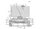
図4Aは、開示される実施形態による、基板処理チャンバ400である。遠隔プラズマシステム(RPS)410がガスを処理してよく、ガスは次いでガス吸入アセンブリ411を介して移動する。2つの別個のガス供給チャネルが、ガス吸入アセンブリ411の内部に認識できる。第1のチャネル412は遠隔プラズマシステムRPS410を通るガスを運び、一方第2のチャネル413はRPS410をバイパスする。開示される実施形態において、第1のチャネル402はプロセスガスのために使用されてよく、第2のチャネル413はトリートメントガスのために使用されてよい。リッド(または導電性上部)421および孔あきパーティション453が、その間にある絶縁リング424とともに示され、絶縁リング424によって、AC電位が孔あきパーティション453を基準にしてリッド421に印加されることを可能にする。プロセスガスは第1のチャネル412を通ってチャンバプラズマ領域420の中に移動し、チャンバプラズマ領域420内のプラズマのみまたはRPS410と組み合わせて励起され得る。本明細書において、チャンバプラズマ領域420および/またはRPS410の組合せは、遠隔プラズマシステムと呼ばれ得る。孔あきパーティション(シャワーヘッドとも呼ばれる)453が、シャワーヘッド453の下の基板処理領域470からチャンバプラズマ領域420を分離する。シャワーヘッド453によって、チャンバプラズマ領域420中に存在するプラズマが基板処理領域470内のガスを直接励起することを回避することを可能にし、一方それでもなお、励起された核種がチャンバプラズマ領域420から基板処理領域470の中に移動することを可能にする。 FIG. 4A is a
シャワーヘッド453は、チャンバプラズマ領域420と基板処理領域470との間に配置され、チャンバプラズマ領域420内で作成されたプラズマ流出物(前駆体または他のガスの励起された誘導体)が、プレートの厚さを横切る複数のスルーホール456を通過することを可能にする。シャワーヘッド453は、蒸気またはガスの形で、前駆体(シリコン含有前駆体など)で充填され、小さな孔455を介して、直接チャンバプラズマ領域420の中にではなく、基板処理領域470の中に通ることができる、1つまたは複数の中空容積451も有する。この開示された実施形態において、シャワーヘッド453は、スルーホール456の最小直径450の長さよりも厚い。チャンバプラズマ領域420から基板処理領域470に浸透する励起された核種の、かなりの濃度を維持するために、スルーホールの最小直径450の長さ426は、シャワーヘッド453を通り抜けるスルーホール456部により長い直径部分を形成することにより制限される場合がある。スルーホール456の最小直径450の長さは、開示された実施形態において、スルーホール456の最小直径と同じ桁数以下であってよい。 The
示された実施形態において、シャワーヘッド453は、チャンバプラズマ領域420内のプラズマにより励起するとすぐ、酸素、水素および/もしくは窒素を含むプロセスガスならびに/またはそのようなプロセスガスのプラズマ流出物を(スルーホール456を介して)散布することができる。実施形態において、RPS410および/またはチャンバプラズマ領域420内で励起されるプロセスガスは、所定の窒素:水素原子流量比をもたらすような相対流量を有する水素(H2)と窒素(N2)を含む。一般的に言って、RPS410および/またはチャンバプラズマ領域420の中に第1のチャネル412を介して導入されるプロセスガスは、酸素(O2)、オゾン(O3)、N2O、NO、NO2、NH3、N2H4を含むNxHy、シラン、ジシラン、TSAおよびDSAのうちの1つまたは複数を含み得る。プロセスガスは、ヘリウム、アルゴン、窒素(N2)などのキャリアガスも含み得る。第2のチャネル413は、成長するまたは堆積したままの膜から不要な構成要素を取り除くために使用される、プロセスガスおよび/もしくはキャリアガスならびに/または膜硬化ガスも送達してよい。プラズマ流出物は、プロセスガスのイオン化されたまたは中性の誘導体を含む場合があり、本明細書において、導入されるプロセスガスの元素構成を意味するラジカル−酸素前駆体および/またはラジカル−窒素前駆体と呼ばれる場合もある。In the illustrated embodiment, as soon as the
実施形態において、スルーホール456の数は、約60と約2000の間であってよい。スルーホール456は、様々な形を有してよいが、最も容易には丸く作られる。スルーホール456の最小直径450は、開示された実施形態において、約0.5mmと約20mmの間または約1mmと約6mmの間であってよい。スルーホールの断面形状の選択にも許容範囲があり、スルーホールの断面形状は、円錐形、円筒形または2つの形状の組合せであってよい。ガスを基板処理領域470の中に導入するために使用される小さな孔455の数は、異なる実施形態において、約100と約5000の間または約500と約2000の間であってよい。小さな孔455の直径は、約0.1mmと約2mmの間であってよい。 In an embodiment, the number of through
図4Bは、開示される実施形態に従う処理チャンバとともに使用するシャワーヘッド453の底面図である。シャワーヘッド453は、図4Aに示されたシャワーヘッドに対応する。スルーホール456は、シャワーヘッド453の底部でより大きな内径(ID)を有し、上部でより小さいIDを有して描かれている。本明細書において記載の他の実施形態よりもさらに均一な混合を可能にする助けとなるスルーホール456の中でも、とりわけ、小さな孔455は、シャワーヘッドの表面全体にわたって実質的に均一に分散される。 FIG. 4B is a bottom view of a
シャワーヘッド453内のスルーホール456を介して到達するプラズマ流出物が、中空容積451から始まる小さな孔455を介して到達するシリコン含有前駆体と化合するとき、例示的な膜が基板処理領域470内のペデスタル(図示せず)によって支持される基板上に作成される。基板処理領域470は、硬化など他のプロセスのためプラズマを支持するように装備されてよいが、例示的な膜の成長期間、プラズマは存在しない。 When the plasma effluent that arrives through the through-
プラズマは、シャワーヘッド453の上のチャンバプラズマ領域420またはシャワーヘッド453の下の基板処理領域470の中で点火されてよい。プラズマは、チャンバプラズマ領域420内に存在し、窒素−水素含有ガスの流入からラジカル窒素前駆体を生成する。典型的には高周波(RF)の範囲であるAC電圧が、堆積の期間、処理チャンバの導電性上部421とシャワーヘッド453との間に印加され、チャンバプラズマ領域420内でプラズマに点火する。RF電力供給は、13.56MHzの高RF周波数を生成するが、単独でまたは13.56MHzの周波数と組み合わせて他の周波数も生成する場合がある。 The plasma may be ignited in the
膜を硬化するため、または基板処理領域470と接する内部表面を洗浄するために、基板処理領域470内の底部プラズマがオンにされるとき、上部プラズマは低電力または無電力のままとされてよい。基板処理領域470内のプラズマは、シャワーヘッド453とペデスタルまたはチャンバの底部との間にAC電圧を印加することにより点火される。洗浄ガスは、プラズマが存在する間に基板処理領域470の中に導入され得る。 When the bottom plasma in the
ペデスタルは、基板の温度を制御するため、熱交換流体がそこを通って流れる、熱交換チャネルを有する場合がある。この構成によって、基板温度が冷却されまたは加熱され、比較的低い温度(室温から約120℃)に維持することを可能にする。熱交換流体は、エチレングリコールおよび水を含んでよい。ペデスタルのウエハ支持プラッタ(好ましくは、アルミニウム、セラミック、またはその組合せ)は、平行同心円の形の、完全な2巻きを作るように構成される、単ループ埋込み型の埋込みヒータ素子を使用して、比較的高い温度(約120℃から約1100℃)を達成するために抵抗加熱もされ得る。ヒータ素子の外側部分は、支持プラッタの周辺に隣接して延びてよく、一方内側部分は、より小さい半径を有する同心円の経路上を延びる。ヒータ素子への配線は、ペデスタルのステムを通過する。 The pedestal may have heat exchange channels through which heat exchange fluid flows to control the temperature of the substrate. This configuration allows the substrate temperature to be cooled or heated and maintained at a relatively low temperature (room temperature to about 120 ° C.). The heat exchange fluid may include ethylene glycol and water. A pedestal wafer support platter (preferably aluminum, ceramic, or a combination thereof) uses a single loop embedded embedded heater element configured to produce two complete turns in the form of parallel concentric circles, Resistive heating can also be done to achieve relatively high temperatures (about 120 ° C. to about 1100 ° C.). The outer portion of the heater element may extend adjacent to the periphery of the support platter, while the inner portion extends on a concentric path having a smaller radius. The wiring to the heater element passes through the pedestal stem.
基板処理システムは、システムコントローラにより制御される。例示的な実施形態において、システムコントローラは、ハードディスクドライブ、フロッピディスクドライブおよびプロセッサを含む。プロセッサはシングルボードコンピュータ(SBC)、アナログおよびデジタル入出力ボード、インターフェースボードおよびステッパモータコントローラボードを含む。CVDシステムの様々な部分は、ボード、カードケージ、ならびにコネクタ寸法および種類を規定するVME(Versa Modular European)規格に適合する。VME規格は、バス構造を、16ビットデータバスおよび24ビットアドレスバスを有するものとしても規定する。 The substrate processing system is controlled by a system controller. In the exemplary embodiment, the system controller includes a hard disk drive, a floppy disk drive, and a processor. The processor includes a single board computer (SBC), analog and digital input / output boards, interface boards and stepper motor controller boards. Various parts of the CVD system meet the VME (Versa Modular European) standard which defines board, card cage, and connector dimensions and types. The VME standard also defines the bus structure as having a 16-bit data bus and a 24-bit address bus.
システムコントローラがCVD機の全ての活動を制御する。システムコントローラは、コンピュータ可読媒体に記憶されたコンピュータプログラムであるシステム制御ソフトウェアを実行する。好ましくは、媒体はハードディスクドライブであるが、媒体が他の種類のメモリであってもよい。コンピュータプログラムは、タイミング、ガスの混合、チャンバ圧力、チャンバ温度、RF電力レベル、サセプタ位置、および特定のプロセスの他のパラメータを定める命令の組を含む。例えば、フロッピディスクまたは他の別の適切なドライブを含む他のメモリデバイス上に記憶された他のコンピュータプログラムが、システムコントローラに命令するために使用されてもよい。 A system controller controls all activities of the CVD machine. The system controller executes system control software, which is a computer program stored on a computer readable medium. Preferably, the medium is a hard disk drive, but the medium may be other types of memory. The computer program includes a set of instructions that define timing, gas mixing, chamber pressure, chamber temperature, RF power level, susceptor position, and other parameters of a particular process. For example, other computer programs stored on other memory devices including a floppy disk or other suitable drive may be used to instruct the system controller.
基板上に積層膜を堆積させるためのプロセス、またはチャンバを洗浄するためのプロセスは、システムコントローラによって実行されるコンピュータプログラム製品を使用して実装されてよい。コンピュータプログラムコードは、例えば、68000アセンブリ言語、C、C++、Pascal、Fortranなど、任意の通常のコンピュータ可読プログラミング言語で書かれてよい。好適なプログラムコードは、通常のテキストエディタを使用して、単一のファイルまたは複数のファイルに入力され、コンピュータのメモリシステムなどコンピュータが使用可能な媒体に記憶されまたは具体化される。入力されたコードテキストが高水準言語である場合、コードはコンパイルされ、結果として得られるコンパイラコードは、次いで事前コンパイルされたMicrosoft Windows(登録商標)ライブラリルーチンのオブジェクトコードとリンクされる。リンクされ、コンパイルされたオブジェクトコードを実行するために、システムユーザがオブジェクトコードを起動し、コンピュータシステムにコードをメモリ中にロードさせる。次いで、CPUがコードを読んで実行し、プログラム中に特定されたタスクを実施する。 The process for depositing the laminated film on the substrate or the process for cleaning the chamber may be implemented using a computer program product executed by the system controller. The computer program code may be written in any conventional computer readable programming language such as, for example, 68000 assembly language, C, C ++, Pascal, Fortran. Suitable program code is entered into a single file or multiple files using a conventional text editor and stored or embodied in a computer usable medium, such as a computer memory system. If the entered code text is in a high level language, the code is compiled and the resulting compiler code is then linked with the precompiled Microsoft Windows library object code. In order to execute the linked and compiled object code, the system user activates the object code and causes the computer system to load the code into memory. The CPU then reads and executes the code and performs the tasks specified in the program.
ユーザとコントローラとの間のインターフェースは、フラットパネル接触式モニタを介する。好ましい実施形態では、2つのモニタが使用され、一方はオペレータ用に洗浄室の壁に取り付けられ、他方は保守技術員用に壁の背後に取り付けられる。2つのモニタは、同じ情報を同時に表示してよく、その場合、一度にただ1つのモニタが入力を受け入れる。特定の画面または機能を選択するために、オペレータは、接触式モニタの指定された区域にタッチする。タッチされた区域は、その強調色を変える、または新しいメニュもしくは画面が表示され、オペレータと接触式モニタとの間の通信を確認する。キーボード、マウス、または他のポインティングデバイスもしくは通信デバイスなどの他のデバイスが、接触式モニタの代わりにまたは接触式モニタに加えて使用され、ユーザがシステムコントローラと通信することを可能にできる。 The interface between the user and the controller is via a flat panel contact monitor. In the preferred embodiment, two monitors are used, one attached to the wall of the washroom for the operator and the other attached behind the wall for the service technician. Two monitors may display the same information simultaneously, in which case only one monitor accepts input at a time. To select a particular screen or function, the operator touches a designated area of the touch monitor. The touched area changes its highlight color or a new menu or screen is displayed confirming communication between the operator and the touch monitor. Other devices such as a keyboard, mouse, or other pointing or communication device can be used in place of or in addition to the touch monitor to allow the user to communicate with the system controller.
本明細書で使用する「基板」は、その上に層を形成された、または形成されていない支持基板であってよい。支持基板は、様々なドーピング濃度およびプロファイルの絶縁体または半導体であってよく、例えば、集積回路の製造において使用される種類の半導体基板であってよい。「酸化ケイ素」の層は、窒素、水素、炭素など、密度の低い他の元素成分を含むことができる。本発明のいくつかの実施形態において、酸化ケイ素は、本質的にシリコンおよび酸素からなる。「励起状態」のガスは、少なくとも一部のガス分子が振動励起し、解離しかつ/またはイオン化した状態であるガスのことを記載する。ガス(または前駆体)は2つ以上のガス(前駆体)の組合せであってよい。用語「トレンチ」は、エッチングされた形状寸法が、大きな水平のアスペクト比を有するという含意なしに、全体にわたって使用される。表面の上から見た場合、トレンチは、円形、長円形、多角形、矩形、または様々な他の形状に見えてよい。用語「ビア」は、低いアスペクト比のトレンチのことを言うために使用され、垂直の電気的接続を形成するために、金属で充填されても充填されなくてもよい。用語「前駆体」は、任意のプロセスガス(または蒸発した液体の液滴)のことを言うために使用され、表面から材料を除去するまたは堆積させるための反応に加わる。 As used herein, a “substrate” may be a supporting substrate with or without a layer formed thereon. The support substrate may be an insulator or semiconductor of various doping concentrations and profiles, for example, a type of semiconductor substrate used in the manufacture of integrated circuits. The “silicon oxide” layer can include other elemental components of low density, such as nitrogen, hydrogen, and carbon. In some embodiments of the invention, the silicon oxide consists essentially of silicon and oxygen. An “excited state” gas describes a gas in which at least some gas molecules are vibrationally excited, dissociated and / or ionized. The gas (or precursor) may be a combination of two or more gases (precursors). The term “trench” is used throughout without the implication that the etched geometry has a large horizontal aspect ratio. When viewed from above the surface, the trenches may appear circular, oval, polygonal, rectangular, or various other shapes. The term “via” is used to refer to a low aspect ratio trench and may or may not be filled with metal to form a vertical electrical connection. The term “precursor” is used to refer to any process gas (or evaporated liquid droplet) and participates in a reaction to remove or deposit material from a surface.
複数の実施形態を記載したが、様々な修正、代替構成、および均等物が、本発明の精神から逸脱することなく使用され得ることが、当業者には理解されよう。加えて、いくつかのよく知られたプロセスおよび要素は、本発明を不必要に曖昧にすることを回避するために記載しなかった。したがって、上の記載が本発明の範囲を限定するものと理解されるべきではない。 While multiple embodiments have been described, those skilled in the art will recognize that various modifications, alternative configurations, and equivalents may be used without departing from the spirit of the invention. In addition, some well-known processes and elements have not been described in order to avoid unnecessarily obscuring the present invention. Accordingly, the above description should not be taken as limiting the scope of the invention.
値の範囲が提供される場合、それぞれの間にある値は、文脈が明らかに別段の規定をしない限り、その範囲の上限と下限との間の下限の単位量の10分の1まで、やはり具体的に開示されると理解される。述べられた範囲内の任意の述べられた値または間にある値と、その述べられた範囲内の任意の他の述べられた値または間にある値の間の、それぞれのより小さい範囲が包含される。述べられた範囲内に具体的に除外される限界があればそれを条件として、これらのより小さい範囲の上限および下限は、独立して範囲内に含まれまたは除外されてよく、限界のいずれかがより小さい範囲内に含まれる場合、限界のどちらもより小さい範囲内に含まれない場合、または両方の限界がより小さい範囲内に含まれる場合、各範囲はやはり本発明に包含される。述べられた範囲が一方または両方の限界を含む場合、それらの含まれる限界のどちらかまたは両方を除外する範囲も含まれる。 Where a range of values is provided, the values between each may be up to one-tenth of the lower unit quantity between the upper and lower limits of the range, unless the context clearly dictates otherwise. It is understood that it is specifically disclosed. Includes each smaller range between any stated value or values within the stated range and any other stated value or values within the stated range. Is done. Subject to any specifically excluded limits within the stated range, the upper and lower limits of these smaller ranges may independently be excluded from any of the limits. Each is also encompassed by the present invention if is included in the smaller range, if neither of the limits is included in the smaller range, or if both limits are included in the smaller range. Where the stated range includes one or both of the limits, ranges excluding either or both of those included limits are also included.
本明細書および添付の特許請求の範囲の中で使用する場合、文脈が明らかに別段の規定をしない限り、単数形の「a」「an」および「the」は、複数形への言及を含む。したがって、例えば、「プロセス(a process)」という言及は、複数のそのようなプロセスを含み、「前駆体(the precursor)」という言及は、1つまたは複数の前駆体および当業者に知られているその均等物を含む。 As used in this specification and the appended claims, the singular forms “a”, “an”, and “the” include references to the plural unless the context clearly dictates otherwise. . Thus, for example, reference to “a process” includes a plurality of such processes, and reference to “the precursor” is known to one or more precursors and those of ordinary skill in the art. Including its equivalent.
さらに、本明細書および後続の特許請求の範囲の中で使用するとき、用語「備える、含む(comprise)」、「備えている、含んでいる(comprising)」、「含む(include)」、「含んでいる(including)」、および「含む(includes)」は、述べた特徴、整数、構成要素、またはステップの存在を明示することを意図するが、1つまたは複数の他の特徴、整数、構成要素、ステップ、行為、またはグループの存在または追加を排除しない。 Further, as used herein and in the claims that follow, the terms “comprising”, “comprising”, “including”, “including”, “ "Including", and "includes" are intended to clarify the presence of the stated feature, integer, component, or step, but one or more other features, integer, Does not exclude the presence or addition of components, steps, acts or groups.
Claims (20)
Translated fromJapanese窒素−水素含有ガスをプラズマ領域の中に流してラジカル−窒素前駆体を生成するステップであって、前記窒素−水素含有ガスが水素(H2)および窒素(N2)を含み、前記プラズマ領域内への窒素:水素原子流量比の選択において、より大きなフレキシビリティを可能にするステップと、
前記無プラズマ基板処理領域内で、シリコン含有前駆体を前記ラジカル−窒素前駆体と化合させるステップと、
前記誘電体層を前記基板上に堆積させるステップと
を含む方法。A method of forming a dielectric layer on a substrate in a plasma-free substrate processing region in a substrate processing chamber, comprising:
Flowing a nitrogen-hydrogen containing gas into a plasma region to generate a radical-nitrogen precursor, wherein the nitrogen-hydrogen containing gas contains hydrogen (H2 ) and nitrogen (N2 ), and the plasma region Allowing greater flexibility in the selection of the nitrogen: hydrogen atom flow ratio into the interior,
Combining a silicon-containing precursor with the radical-nitrogen precursor in the plasma-free substrate processing region;
Depositing the dielectric layer on the substrate.
Applications Claiming Priority (5)
| Application Number | Priority Date | Filing Date | Title |
|---|---|---|---|
| US29105409P | 2009-12-30 | 2009-12-30 | |
| US61/291,054 | 2009-12-30 | ||
| US12/969,877US8629067B2 (en) | 2009-12-30 | 2010-12-16 | Dielectric film growth with radicals produced using flexible nitrogen/hydrogen ratio |
| US12/969,877 | 2010-12-16 | ||
| PCT/US2010/060852WO2011090626A2 (en) | 2009-12-30 | 2010-12-16 | Dielectric film growth with radicals produced using flexible nitrogen/hydrogen ratio |
Publications (1)
| Publication Number | Publication Date |
|---|---|
| JP2013516763Atrue JP2013516763A (en) | 2013-05-13 |
Family
ID=44188077
Family Applications (1)
| Application Number | Title | Priority Date | Filing Date |
|---|---|---|---|
| JP2012547117AWithdrawnJP2013516763A (en) | 2009-12-30 | 2010-12-16 | Dielectric film growth using radicals generated using a flexible nitrogen / hydrogen ratio |
Country Status (7)
| Country | Link |
|---|---|
| US (1) | US8629067B2 (en) |
| JP (1) | JP2013516763A (en) |
| KR (1) | KR20120111738A (en) |
| CN (1) | CN102687252A (en) |
| SG (1) | SG181670A1 (en) |
| TW (1) | TW201131653A (en) |
| WO (1) | WO2011090626A2 (en) |
Families Citing this family (41)
| Publication number | Priority date | Publication date | Assignee | Title |
|---|---|---|---|---|
| US8232176B2 (en) | 2006-06-22 | 2012-07-31 | Applied Materials, Inc. | Dielectric deposition and etch back processes for bottom up gapfill |
| US7867923B2 (en)* | 2007-10-22 | 2011-01-11 | Applied Materials, Inc. | High quality silicon oxide films by remote plasma CVD from disilane precursors |
| US8357435B2 (en) | 2008-05-09 | 2013-01-22 | Applied Materials, Inc. | Flowable dielectric equipment and processes |
| US8980382B2 (en) | 2009-12-02 | 2015-03-17 | Applied Materials, Inc. | Oxygen-doping for non-carbon radical-component CVD films |
| US8741788B2 (en) | 2009-08-06 | 2014-06-03 | Applied Materials, Inc. | Formation of silicon oxide using non-carbon flowable CVD processes |
| US8449942B2 (en) | 2009-11-12 | 2013-05-28 | Applied Materials, Inc. | Methods of curing non-carbon flowable CVD films |
| US8329262B2 (en) | 2010-01-05 | 2012-12-11 | Applied Materials, Inc. | Dielectric film formation using inert gas excitation |
| SG182336A1 (en) | 2010-01-06 | 2012-08-30 | Applied Materials Inc | Flowable dielectric using oxide liner |
| KR101837648B1 (en) | 2010-01-07 | 2018-04-19 | 어플라이드 머티어리얼스, 인코포레이티드 | Insitu ozone cure for radicalcomponent cvd |
| JP2013521650A (en) | 2010-03-05 | 2013-06-10 | アプライド マテリアルズ インコーポレイテッド | Conformal layer by radical component CVD |
| US9285168B2 (en) | 2010-10-05 | 2016-03-15 | Applied Materials, Inc. | Module for ozone cure and post-cure moisture treatment |
| US8664127B2 (en) | 2010-10-15 | 2014-03-04 | Applied Materials, Inc. | Two silicon-containing precursors for gapfill enhancing dielectric liner |
| US10283321B2 (en) | 2011-01-18 | 2019-05-07 | Applied Materials, Inc. | Semiconductor processing system and methods using capacitively coupled plasma |
| US8450191B2 (en) | 2011-01-24 | 2013-05-28 | Applied Materials, Inc. | Polysilicon films by HDP-CVD |
| US8716154B2 (en) | 2011-03-04 | 2014-05-06 | Applied Materials, Inc. | Reduced pattern loading using silicon oxide multi-layers |
| US8445078B2 (en) | 2011-04-20 | 2013-05-21 | Applied Materials, Inc. | Low temperature silicon oxide conversion |
| US8466073B2 (en) | 2011-06-03 | 2013-06-18 | Applied Materials, Inc. | Capping layer for reduced outgassing |
| US9404178B2 (en) | 2011-07-15 | 2016-08-02 | Applied Materials, Inc. | Surface treatment and deposition for reduced outgassing |
| US8617989B2 (en) | 2011-09-26 | 2013-12-31 | Applied Materials, Inc. | Liner property improvement |
| US8551891B2 (en) | 2011-10-04 | 2013-10-08 | Applied Materials, Inc. | Remote plasma burn-in |
| US8889566B2 (en) | 2012-09-11 | 2014-11-18 | Applied Materials, Inc. | Low cost flowable dielectric films |
| US9165783B2 (en)* | 2012-11-01 | 2015-10-20 | Applied Materials, Inc. | Method of patterning a low-k dielectric film |
| US9018108B2 (en)* | 2013-01-25 | 2015-04-28 | Applied Materials, Inc. | Low shrinkage dielectric films |
| US9564309B2 (en) | 2013-03-14 | 2017-02-07 | Asm Ip Holding B.V. | Si precursors for deposition of SiN at low temperatures |
| US20150167160A1 (en)* | 2013-12-16 | 2015-06-18 | Applied Materials, Inc. | Enabling radical-based deposition of dielectric films |
| US9412581B2 (en) | 2014-07-16 | 2016-08-09 | Applied Materials, Inc. | Low-K dielectric gapfill by flowable deposition |
| US9576792B2 (en) | 2014-09-17 | 2017-02-21 | Asm Ip Holding B.V. | Deposition of SiN |
| US9355922B2 (en) | 2014-10-14 | 2016-05-31 | Applied Materials, Inc. | Systems and methods for internal surface conditioning in plasma processing equipment |
| US9966240B2 (en) | 2014-10-14 | 2018-05-08 | Applied Materials, Inc. | Systems and methods for internal surface conditioning assessment in plasma processing equipment |
| US20160225652A1 (en) | 2015-02-03 | 2016-08-04 | Applied Materials, Inc. | Low temperature chuck for plasma processing systems |
| US10410857B2 (en) | 2015-08-24 | 2019-09-10 | Asm Ip Holding B.V. | Formation of SiN thin films |
| KR102458309B1 (en) | 2015-12-28 | 2022-10-24 | 삼성전자주식회사 | Method of forming a SiOCN material layer and method of fabricating a semiconductor device |
| US10468244B2 (en) | 2016-08-30 | 2019-11-05 | Versum Materials Us, Llc | Precursors and flowable CVD methods for making low-K films to fill surface features |
| US11017998B2 (en) | 2016-08-30 | 2021-05-25 | Versum Materials Us, Llc | Precursors and flowable CVD methods for making low-K films to fill surface features |
| US11735413B2 (en) | 2016-11-01 | 2023-08-22 | Versum Materials Us, Llc | Precursors and flowable CVD methods for making low-k films to fill surface features |
| US10453678B2 (en)* | 2017-04-13 | 2019-10-22 | Applied Materials, Inc. | Method and apparatus for deposition of low-k films |
| US10872762B2 (en)* | 2017-11-08 | 2020-12-22 | Taiwan Semiconductor Manufacturing Company, Ltd. | Methods of forming silicon oxide layer and semiconductor structure |
| WO2019147462A1 (en)* | 2018-01-26 | 2019-08-01 | Applied Materials, Inc. | Treatment methods for silicon nitride thin films |
| US10580645B2 (en)* | 2018-04-30 | 2020-03-03 | Asm Ip Holding B.V. | Plasma enhanced atomic layer deposition (PEALD) of SiN using silicon-hydrohalide precursors |
| US20200058497A1 (en)* | 2018-08-20 | 2020-02-20 | Applied Materials, Inc | Silicon nitride forming precursor control |
| KR20220081905A (en) | 2020-12-09 | 2022-06-16 | 에이에스엠 아이피 홀딩 비.브이. | Silicon precursors for silicon silicon nitride deposition |
Family Cites Families (360)
| Publication number | Priority date | Publication date | Assignee | Title |
|---|---|---|---|---|
| US4147571A (en) | 1977-07-11 | 1979-04-03 | Hewlett-Packard Company | Method for vapor epitaxial deposition of III/V materials utilizing organometallic compounds and a halogen or halide in a hot wall system |
| US4200666A (en) | 1978-08-02 | 1980-04-29 | Texas Instruments Incorporated | Single component monomer for silicon nitride deposition |
| FR2598520B1 (en) | 1986-01-21 | 1994-01-28 | Seiko Epson Corp | MINERAL PROTECTIVE FILM |
| US4946593A (en) | 1987-03-31 | 1990-08-07 | Acushnet Company | Rubber composition for use with potable water |
| US4818326A (en) | 1987-07-16 | 1989-04-04 | Texas Instruments Incorporated | Processing apparatus |
| US4816098A (en) | 1987-07-16 | 1989-03-28 | Texas Instruments Incorporated | Apparatus for transferring workpieces |
| US4910043A (en)* | 1987-07-16 | 1990-03-20 | Texas Instruments Incorporated | Processing apparatus and method |
| US4931354A (en) | 1987-11-02 | 1990-06-05 | Murata Manufacturing Co., Ltd. | Multilayer printed circuit board |
| JPH03257182A (en) | 1990-03-07 | 1991-11-15 | Hitachi Ltd | surface processing equipment |
| US5016332A (en) | 1990-04-13 | 1991-05-21 | Branson International Plasma Corporation | Plasma reactor and process with wafer temperature control |
| US5620525A (en) | 1990-07-16 | 1997-04-15 | Novellus Systems, Inc. | Apparatus for supporting a substrate and introducing gas flow doximate to an edge of the substrate |
| US5843233A (en) | 1990-07-16 | 1998-12-01 | Novellus Systems, Inc. | Exclusion guard and gas-based substrate protection for chemical vapor deposition apparatus |
| US5578532A (en) | 1990-07-16 | 1996-11-26 | Novellus Systems, Inc. | Wafer surface protection in a gas deposition process |
| KR930009549B1 (en)* | 1990-11-28 | 1993-10-06 | 현대전자산업 주식회사 | How to maintain resistance of high-resistance polycrystalline silicon |
| US5436172A (en) | 1991-05-20 | 1995-07-25 | Texas Instruments Incorporated | Real-time multi-zone semiconductor wafer temperature and process uniformity control system |
| US5426076A (en) | 1991-07-16 | 1995-06-20 | Intel Corporation | Dielectric deposition and cleaning process for improved gap filling and device planarization |
| US5279784A (en) | 1992-05-05 | 1994-01-18 | Bandag Licensing Corporation | Method of fabrication of composite tire thread |
| US5271972A (en) | 1992-08-17 | 1993-12-21 | Applied Materials, Inc. | Method for depositing ozone/TEOS silicon oxide films of reduced surface sensitivity |
| US5393708A (en) | 1992-10-08 | 1995-02-28 | Industrial Technology Research Institute | Inter-metal-dielectric planarization process |
| JP2684942B2 (en) | 1992-11-30 | 1997-12-03 | 日本電気株式会社 | Chemical vapor deposition method, chemical vapor deposition apparatus, and method for manufacturing multilayer wiring |
| US5377139A (en) | 1992-12-11 | 1994-12-27 | Motorola, Inc. | Process forming an integrated circuit |
| US5434109A (en)* | 1993-04-27 | 1995-07-18 | International Business Machines Corporation | Oxidation of silicon nitride in semiconductor devices |
| US5587014A (en) | 1993-12-22 | 1996-12-24 | Sumitomo Chemical Company, Limited | Method for manufacturing group III-V compound semiconductor crystals |
| US5679152A (en) | 1994-01-27 | 1997-10-21 | Advanced Technology Materials, Inc. | Method of making a single crystals Ga*N article |
| US5547703A (en) | 1994-04-11 | 1996-08-20 | Dow Corning Corporation | Method of forming si-o containing coatings |
| US5468687A (en) | 1994-07-27 | 1995-11-21 | International Business Machines Corporation | Method of making TA2 O5 thin film by low temperature ozone plasma annealing (oxidation) |
| US5576071A (en) | 1994-11-08 | 1996-11-19 | Micron Technology, Inc. | Method of reducing carbon incorporation into films produced by chemical vapor deposition involving organic precursor compounds |
| JPH08148559A (en) | 1994-11-15 | 1996-06-07 | Fujitsu Ltd | Method for manufacturing semiconductor device having insulating film |
| US5530293A (en)* | 1994-11-28 | 1996-06-25 | International Business Machines Corporation | Carbon-free hydrogen silsesquioxane with dielectric constant less than 3.2 annealed in hydrogen for integrated circuits |
| US5558717A (en) | 1994-11-30 | 1996-09-24 | Applied Materials | CVD Processing chamber |
| US5786263A (en) | 1995-04-04 | 1998-07-28 | Motorola, Inc. | Method for forming a trench isolation structure in an integrated circuit |
| US5966595A (en) | 1995-10-05 | 1999-10-12 | Micron Technology, Inc. | Method to form a DRAM capacitor using low temperature reoxidation |
| JPH09237785A (en) | 1995-12-28 | 1997-09-09 | Toshiba Corp | Semiconductor device and manufacturing method thereof |
| JP2871580B2 (en)* | 1996-03-29 | 1999-03-17 | 日本電気株式会社 | Method for manufacturing semiconductor device |
| US6070551A (en) | 1996-05-13 | 2000-06-06 | Applied Materials, Inc. | Deposition chamber and method for depositing low dielectric constant films |
| US5827783A (en) | 1996-08-23 | 1998-10-27 | Mosel Vitelic, Inc. | Stacked capacitor having improved charge storage capacity |
| US5935340A (en) | 1996-11-13 | 1999-08-10 | Applied Materials, Inc. | Method and apparatus for gettering fluorine from chamber material surfaces |
| US5873781A (en) | 1996-11-14 | 1999-02-23 | Bally Gaming International, Inc. | Gaming machine having truly random results |
| US5811325A (en) | 1996-12-31 | 1998-09-22 | Industrial Technology Research Institute | Method of making a polysilicon carbon source/drain heterojunction thin-film transistor |
| US6090723A (en) | 1997-02-10 | 2000-07-18 | Micron Technology, Inc. | Conditioning of dielectric materials |
| FR2759362B1 (en) | 1997-02-10 | 1999-03-12 | Saint Gobain Vitrage | TRANSPARENT SUBSTRATE EQUIPPED WITH AT LEAST ONE THIN LAYER BASED ON SILICON NITRIDE OR OXYNITRIDE AND ITS PROCESS FOR OBTAINING IT |
| TW388100B (en) | 1997-02-18 | 2000-04-21 | Hitachi Ulsi Eng Corp | Semiconductor deivce and process for producing the same |
| US5937308A (en) | 1997-03-26 | 1999-08-10 | Advanced Micro Devices, Inc. | Semiconductor trench isolation structure formed substantially within a single chamber |
| US6090442A (en)* | 1997-04-14 | 2000-07-18 | University Technology Corporation | Method of growing films on substrates at room temperatures using catalyzed binary reaction sequence chemistry |
| US6551665B1 (en) | 1997-04-17 | 2003-04-22 | Micron Technology, Inc. | Method for improving thickness uniformity of deposited ozone-TEOS silicate glass layers |
| US5937323A (en) | 1997-06-03 | 1999-08-10 | Applied Materials, Inc. | Sequencing of the recipe steps for the optimal low-k HDP-CVD processing |
| US6207587B1 (en) | 1997-06-24 | 2001-03-27 | Micron Technology, Inc. | Method for forming a dielectric |
| TW416100B (en) | 1997-07-02 | 2000-12-21 | Applied Materials Inc | Control of oxygen to silane ratio in a seasoning process to improve particle performance in an HDP-CVD system |
| US6114219A (en) | 1997-09-15 | 2000-09-05 | Advanced Micro Devices, Inc. | Method of manufacturing an isolation region in a semiconductor device using a flowable oxide-generating material |
| US6024044A (en) | 1997-10-09 | 2000-02-15 | Applied Komatsu Technology, Inc. | Dual frequency excitation of plasma for film deposition |
| US6624064B1 (en) | 1997-10-10 | 2003-09-23 | Applied Materials, Inc. | Chamber seasoning method to improve adhesion of F-containing dielectric film to metal for VLSI application |
| US6566281B1 (en) | 1997-10-15 | 2003-05-20 | International Business Machines Corporation | Nitrogen-rich barrier layer and structures formed |
| US6087243A (en) | 1997-10-21 | 2000-07-11 | Advanced Micro Devices, Inc. | Method of forming trench isolation with high integrity, ultra thin gate oxide |
| US6017791A (en) | 1997-11-10 | 2000-01-25 | Taiwan Semiconductor Manufacturing Company | Multi-layer silicon nitride deposition method for forming low oxidation temperature thermally oxidized silicon nitride/silicon oxide (no) layer |
| JP3141827B2 (en) | 1997-11-20 | 2001-03-07 | 日本電気株式会社 | Method for manufacturing semiconductor device |
| US6009830A (en) | 1997-11-21 | 2000-01-04 | Applied Materials Inc. | Independent gas feeds in a plasma reactor |
| KR100253079B1 (en) | 1997-12-01 | 2000-04-15 | 윤종용 | Semiconductor element trench isolation method |
| US6054379A (en)* | 1998-02-11 | 2000-04-25 | Applied Materials, Inc. | Method of depositing a low k dielectric with organo silane |
| US6413583B1 (en) | 1998-02-11 | 2002-07-02 | Applied Materials, Inc. | Formation of a liquid-like silica layer by reaction of an organosilicon compound and a hydroxyl forming compound |
| US6156394A (en) | 1998-04-17 | 2000-12-05 | Optical Coating Laboratory, Inc. | Polymeric optical substrate method of treatment |
| US6068884A (en) | 1998-04-28 | 2000-05-30 | Silcon Valley Group Thermal Systems, Llc | Method of making low κ dielectric inorganic/organic hybrid films |
| US6165834A (en) | 1998-05-07 | 2000-12-26 | Micron Technology, Inc. | Method of forming capacitors, method of processing dielectric layers, method of forming a DRAM cell |
| US6509283B1 (en) | 1998-05-13 | 2003-01-21 | National Semiconductor Corporation | Thermal oxidation method utilizing atomic oxygen to reduce dangling bonds in silicon dioxide grown on silicon |
| US6146970A (en) | 1998-05-26 | 2000-11-14 | Motorola Inc. | Capped shallow trench isolation and method of formation |
| US6187682B1 (en) | 1998-05-26 | 2001-02-13 | Motorola Inc. | Inert plasma gas surface cleaning process performed insitu with physical vapor deposition (PVD) of a layer of material |
| US6667553B2 (en) | 1998-05-29 | 2003-12-23 | Dow Corning Corporation | H:SiOC coated substrates |
| US6461970B1 (en) | 1998-06-10 | 2002-10-08 | Micron Technology, Inc. | Method of reducing defects in anti-reflective coatings and semiconductor structures fabricated thereby |
| US6302964B1 (en) | 1998-06-16 | 2001-10-16 | Applied Materials, Inc. | One-piece dual gas faceplate for a showerhead in a semiconductor wafer processing system |
| US6014979A (en)* | 1998-06-22 | 2000-01-18 | Applied Materials, Inc. | Localizing cleaning plasma for semiconductor processing |
| US6406677B1 (en) | 1998-07-22 | 2002-06-18 | Eltron Research, Inc. | Methods for low and ambient temperature preparation of precursors of compounds of group III metals and group V elements |
| US6410149B1 (en)* | 1998-08-27 | 2002-06-25 | Alliedsignal Inc. | Silane-based nanoporous silica thin films and precursors for making same |
| US6800571B2 (en) | 1998-09-29 | 2004-10-05 | Applied Materials Inc. | CVD plasma assisted low dielectric constant films |
| US6197658B1 (en) | 1998-10-30 | 2001-03-06 | Taiwan Semiconductor Manufacturing Company | Sub-atmospheric pressure thermal chemical vapor deposition (SACVD) trench isolation method with attenuated surface sensitivity |
| US6245690B1 (en) | 1998-11-04 | 2001-06-12 | Applied Materials, Inc. | Method of improving moisture resistance of low dielectric constant films |
| US6121130A (en) | 1998-11-16 | 2000-09-19 | Chartered Semiconductor Manufacturing Ltd. | Laser curing of spin-on dielectric thin films |
| US6583063B1 (en)* | 1998-12-03 | 2003-06-24 | Applied Materials, Inc. | Plasma etching of silicon using fluorinated gas mixtures |
| TW445570B (en)* | 1998-12-11 | 2001-07-11 | United Microelectronics Corp | Manufacturing method for shallow trench isolation |
| US6469283B1 (en) | 1999-03-04 | 2002-10-22 | Applied Materials, Inc. | Method and apparatus for reducing thermal gradients within a substrate support |
| US6290774B1 (en) | 1999-05-07 | 2001-09-18 | Cbl Technology, Inc. | Sequential hydride vapor phase epitaxy |
| US7091605B2 (en)* | 2001-09-21 | 2006-08-15 | Eastman Kodak Company | Highly moisture-sensitive electronic device element and method for fabrication |
| US6180490B1 (en) | 1999-05-25 | 2001-01-30 | Chartered Semiconductor Manufacturing Ltd. | Method of filling shallow trenches |
| US6204201B1 (en) | 1999-06-11 | 2001-03-20 | Electron Vision Corporation | Method of processing films prior to chemical vapor deposition using electron beam processing |
| US6524931B1 (en) | 1999-07-20 | 2003-02-25 | Motorola, Inc. | Method for forming a trench isolation structure in an integrated circuit |
| US6383954B1 (en) | 1999-07-27 | 2002-05-07 | Applied Materials, Inc. | Process gas distribution for forming stable fluorine-doped silicate glass and other films |
| US6602806B1 (en) | 1999-08-17 | 2003-08-05 | Applied Materials, Inc. | Thermal CVD process for depositing a low dielectric constant carbon-doped silicon oxide film |
| US6875687B1 (en)* | 1999-10-18 | 2005-04-05 | Applied Materials, Inc. | Capping layer for extreme low dielectric constant films |
| DE60025872T2 (en) | 1999-10-25 | 2006-08-17 | Dow Corning Corp., Midland | Soluble silicone resin compositions |
| US6682659B1 (en) | 1999-11-08 | 2004-01-27 | Taiwan Semiconductor Manufacturing Company | Method for forming corrosion inhibited conductor layer |
| JP2001144325A (en) | 1999-11-12 | 2001-05-25 | Sony Corp | Method of manufacturing nitride iii-v compound semiconductor and semiconductor device |
| FI118804B (en)* | 1999-12-03 | 2008-03-31 | Asm Int | Process for making oxide films |
| US6348420B1 (en) | 1999-12-23 | 2002-02-19 | Asm America, Inc. | Situ dielectric stacks |
| US6150286A (en) | 2000-01-03 | 2000-11-21 | Advanced Micro Devices, Inc. | Method of making an ultra thin silicon nitride film |
| US6440860B1 (en)* | 2000-01-18 | 2002-08-27 | Micron Technology, Inc. | Semiconductor processing methods of transferring patterns from patterned photoresists to materials, and structures comprising silicon nitride |
| US6541367B1 (en) | 2000-01-18 | 2003-04-01 | Applied Materials, Inc. | Very low dielectric constant plasma-enhanced CVD films |
| US6461980B1 (en) | 2000-01-28 | 2002-10-08 | Applied Materials, Inc. | Apparatus and process for controlling the temperature of a substrate in a plasma reactor chamber |
| EP1124252A2 (en) | 2000-02-10 | 2001-08-16 | Applied Materials, Inc. | Apparatus and process for processing substrates |
| EP1130633A1 (en) | 2000-02-29 | 2001-09-05 | STMicroelectronics S.r.l. | A method of depositing silicon oxynitride polimer layers |
| US7419903B2 (en) | 2000-03-07 | 2008-09-02 | Asm International N.V. | Thin films |
| US6558755B2 (en) | 2000-03-20 | 2003-05-06 | Dow Corning Corporation | Plasma curing process for porous silica thin film |
| TWI250968B (en) | 2000-04-04 | 2006-03-11 | Asahi Kasei Corp | Coating composition for use in producing a silica insulating thin film and method for producing a silica insulating thin film |
| US6630413B2 (en) | 2000-04-28 | 2003-10-07 | Asm Japan K.K. | CVD syntheses of silicon nitride materials |
| US6387207B1 (en) | 2000-04-28 | 2002-05-14 | Applied Materials, Inc. | Integration of remote plasma generator with semiconductor processing chamber |
| US6495479B1 (en)* | 2000-05-05 | 2002-12-17 | Honeywell International, Inc. | Simplified method to produce nanoporous silicon-based films |
| US6553932B2 (en) | 2000-05-12 | 2003-04-29 | Applied Materials, Inc. | Reduction of plasma edge effect on plasma enhanced CVD processes |
| US6559026B1 (en) | 2000-05-25 | 2003-05-06 | Applied Materials, Inc | Trench fill with HDP-CVD process including coupled high power density plasma deposition |
| JP4371543B2 (en) | 2000-06-29 | 2009-11-25 | 日本電気株式会社 | Remote plasma CVD apparatus and film forming method |
| TW533489B (en)* | 2000-06-30 | 2003-05-21 | Hitachi Ltd | Semiconductor device and production method thereof |
| US6835278B2 (en) | 2000-07-07 | 2004-12-28 | Mattson Technology Inc. | Systems and methods for remote plasma clean |
| US7183177B2 (en)* | 2000-08-11 | 2007-02-27 | Applied Materials, Inc. | Silicon-on-insulator wafer transfer method using surface activation plasma immersion ion implantation for wafer-to-wafer adhesion enhancement |
| US6614181B1 (en) | 2000-08-23 | 2003-09-02 | Applied Materials, Inc. | UV radiation source for densification of CVD carbon-doped silicon oxide films |
| US6566278B1 (en) | 2000-08-24 | 2003-05-20 | Applied Materials Inc. | Method for densification of CVD carbon-doped silicon oxide films through UV irradiation |
| US6682969B1 (en)* | 2000-08-31 | 2004-01-27 | Micron Technology, Inc. | Top electrode in a strongly oxidizing environment |
| US6706634B1 (en) | 2000-09-19 | 2004-03-16 | Infineon Technologies Ag | Control of separation between transfer gate and storage node in vertical DRAM |
| JP4232330B2 (en) | 2000-09-22 | 2009-03-04 | 東京エレクトロン株式会社 | Excited gas forming apparatus, processing apparatus and processing method |
| JP3712356B2 (en) | 2000-10-23 | 2005-11-02 | アプライド マテリアルズ インコーポレイテッド | Film-forming method and semiconductor device manufacturing method |
| US20020060322A1 (en) | 2000-11-20 | 2002-05-23 | Hiroshi Tanabe | Thin film transistor having high mobility and high on-current and method for manufacturing the same |
| US6287962B1 (en) | 2000-11-30 | 2001-09-11 | Taiwan Semiconductor Manufacturing Company | Method for making a novel graded silicon nitride/silicon oxide (SNO) hard mask for improved deep sub-micrometer semiconductor processing |
| US6531413B2 (en)* | 2000-12-05 | 2003-03-11 | United Microelectronics Corp. | Method for depositing an undoped silicate glass layer |
| KR100385947B1 (en) | 2000-12-06 | 2003-06-02 | 삼성전자주식회사 | Method of forming thin film by atomic layer deposition |
| US6576564B2 (en)* | 2000-12-07 | 2003-06-10 | Micron Technology, Inc. | Photo-assisted remote plasma apparatus and method |
| US6930041B2 (en) | 2000-12-07 | 2005-08-16 | Micron Technology, Inc. | Photo-assisted method for semiconductor fabrication |
| US6538274B2 (en)* | 2000-12-20 | 2003-03-25 | Micron Technology, Inc. | Reduction of damage in semiconductor container capacitors |
| US20020081817A1 (en) | 2000-12-22 | 2002-06-27 | Jayendra Bhakta | Void reduction and increased throughput in trench fill processes |
| US6660662B2 (en) | 2001-01-26 | 2003-12-09 | Applied Materials, Inc. | Method of reducing plasma charge damage for plasma processes |
| US6599839B1 (en)* | 2001-02-02 | 2003-07-29 | Advanced Micro Devices, Inc. | Plasma etch process for nonhomogenous film |
| US6589868B2 (en)* | 2001-02-08 | 2003-07-08 | Applied Materials, Inc. | Si seasoning to reduce particles, extend clean frequency, block mobile ions and increase chamber throughput |
| KR100364026B1 (en)* | 2001-02-22 | 2002-12-11 | 삼성전자 주식회사 | Method for forming inter layer dielectric film |
| US6632478B2 (en) | 2001-02-22 | 2003-10-14 | Applied Materials, Inc. | Process for forming a low dielectric constant carbon-containing film |
| US6447651B1 (en) | 2001-03-07 | 2002-09-10 | Applied Materials, Inc. | High-permeability magnetic shield for improved process uniformity in nonmagnetized plasma process chambers |
| JP3990920B2 (en) | 2001-03-13 | 2007-10-17 | 東京エレクトロン株式会社 | Film forming method and film forming apparatus |
| KR100897771B1 (en) | 2001-03-13 | 2009-05-15 | 도쿄엘렉트론가부시키가이샤 | Film forming method and film forming apparatus |
| JP3924483B2 (en) | 2001-03-19 | 2007-06-06 | アイピーエス リミテッド | Chemical vapor deposition equipment |
| US6593248B2 (en) | 2001-03-23 | 2003-07-15 | Dow Corning Corporation | Method for producing hydrogenated silicon oxycarbide films having low dielectric constant |
| US6596576B2 (en) | 2001-04-10 | 2003-07-22 | Applied Materials, Inc. | Limiting hydrogen ion diffusion using multiple layers of SiO2 and Si3N4 |
| FR2824062B1 (en)* | 2001-04-27 | 2004-10-15 | Atofina | PROCESS FOR PRODUCING AQUEOUS SOLUTIONS OF QUATERNARY AMMONIUM UNSATURATED SALTS |
| US6528332B2 (en) | 2001-04-27 | 2003-03-04 | Advanced Micro Devices, Inc. | Method and system for reducing polymer build up during plasma etch of an intermetal dielectric |
| US6780499B2 (en) | 2001-05-03 | 2004-08-24 | International Business Machines Corporation | Ordered two-phase dielectric film, and semiconductor device containing the same |
| US6596653B2 (en) | 2001-05-11 | 2003-07-22 | Applied Materials, Inc. | Hydrogen assisted undoped silicon oxide deposition process for HDP-CVD |
| US6716770B2 (en) | 2001-05-23 | 2004-04-06 | Air Products And Chemicals, Inc. | Low dielectric constant material and method of processing by CVD |
| US20020182893A1 (en) | 2001-06-05 | 2002-12-05 | International Business Machines Corporation | Oxidation of silicon nitride films in semiconductor devices |
| JP2003017556A (en) | 2001-06-29 | 2003-01-17 | Mitsubishi Electric Corp | Semiconductor device and method of manufacturing the same |
| KR100421046B1 (en) | 2001-07-13 | 2004-03-04 | 삼성전자주식회사 | Semiconductor device and method for manufacturing the same |
| US6548416B2 (en) | 2001-07-24 | 2003-04-15 | Axcelis Technolgoies, Inc. | Plasma ashing process |
| SG169225A1 (en) | 2001-07-25 | 2011-03-30 | Univ Princeton | Nanochannel arrays and their preparation and use for high throughput macromolecular analysis |
| US6596654B1 (en) | 2001-08-24 | 2003-07-22 | Novellus Systems, Inc. | Gap fill for high aspect ratio structures |
| US20030064154A1 (en) | 2001-08-06 | 2003-04-03 | Laxman Ravi K. | Low-K dielectric thin films and chemical vapor deposition method of making same |
| US6531412B2 (en) | 2001-08-10 | 2003-03-11 | International Business Machines Corporation | Method for low temperature chemical vapor deposition of low-k films using selected cyclosiloxane and ozone gases for semiconductor applications |
| KR100428768B1 (en) | 2001-08-29 | 2004-04-30 | 삼성전자주식회사 | Sti type semiconductor device and method of forming the same |
| US6756085B2 (en) | 2001-09-14 | 2004-06-29 | Axcelis Technologies, Inc. | Ultraviolet curing processes for advanced low-k materials |
| US6872323B1 (en)* | 2001-11-01 | 2005-03-29 | Novellus Systems, Inc. | In situ plasma process to remove fluorine residues from the interior surfaces of a CVD reactor |
| US6770521B2 (en) | 2001-11-30 | 2004-08-03 | Texas Instruments Incorporated | Method of making multiple work function gates by implanting metals with metallic alloying additives |
| US6794290B1 (en) | 2001-12-03 | 2004-09-21 | Novellus Systems, Inc. | Method of chemical modification of structure topography |
| JP3617497B2 (en) | 2001-12-25 | 2005-02-02 | 松下電器産業株式会社 | Ultrasonic bonding apparatus and ultrasonic bonding method |
| JP3891267B2 (en) | 2001-12-25 | 2007-03-14 | キヤノンアネルバ株式会社 | Silicon oxide film manufacturing method |
| US20030124873A1 (en) | 2001-12-28 | 2003-07-03 | Guangcai Xing | Method of annealing an oxide film |
| JP2003204063A (en) | 2002-01-10 | 2003-07-18 | Toshiba Corp | Semiconductor device and manufacturing method thereof |
| AU2003238853A1 (en) | 2002-01-25 | 2003-09-02 | Applied Materials, Inc. | Apparatus for cyclical deposition of thin films |
| US6911391B2 (en) | 2002-01-26 | 2005-06-28 | Applied Materials, Inc. | Integration of titanium and titanium nitride layers |
| US6998014B2 (en)* | 2002-01-26 | 2006-02-14 | Applied Materials, Inc. | Apparatus and method for plasma assisted deposition |
| JP3868324B2 (en) | 2002-04-15 | 2007-01-17 | 三菱電機株式会社 | Silicon nitride film forming method, film forming apparatus, and semiconductor device manufacturing method |
| TW536775B (en) | 2002-04-18 | 2003-06-11 | Nanya Technology Corp | Manufacturing method of shallow trench isolation structure |
| AU2003235305A1 (en) | 2002-04-19 | 2003-11-03 | Tokyo Electron Limited | Method of treating substrate and process for producing semiconductor device |
| KR100468729B1 (en)* | 2002-04-25 | 2005-01-29 | 삼성전자주식회사 | Method for Atomic Layer Deposition of silicon oxide film using HCD source |
| US6936551B2 (en) | 2002-05-08 | 2005-08-30 | Applied Materials Inc. | Methods and apparatus for E-beam treatment used to fabricate integrated circuit devices |
| US7307273B2 (en) | 2002-06-07 | 2007-12-11 | Amberwave Systems Corporation | Control of strain in device layers by selective relaxation |
| TWI283899B (en) | 2002-07-09 | 2007-07-11 | Applied Materials Inc | Capacitively coupled plasma reactor with magnetic plasma control |
| US6900881B2 (en) | 2002-07-11 | 2005-05-31 | Molecular Imprints, Inc. | Step and repeat imprint lithography systems |
| US7294582B2 (en)* | 2002-07-19 | 2007-11-13 | Asm International, N.V. | Low temperature silicon compound deposition |
| US6734082B2 (en)* | 2002-08-06 | 2004-05-11 | Chartered Semiconductor Manufacturing Ltd. | Method of forming a shallow trench isolation structure featuring a group of insulator liner layers located on the surfaces of a shallow trench shape |
| US6825097B2 (en)* | 2002-08-07 | 2004-11-30 | International Business Machines Corporation | Triple oxide fill for trench isolation |
| JP2004095889A (en) | 2002-08-30 | 2004-03-25 | Fasl Japan Ltd | Semiconductor storage device and method of manufacturing the same |
| KR100459724B1 (en)* | 2002-09-11 | 2004-12-03 | 삼성전자주식회사 | Semiconductor device having a SiN etch stopper by low temperature ALD and fabricating method the same |
| US7335609B2 (en)* | 2004-08-27 | 2008-02-26 | Applied Materials, Inc. | Gap-fill depositions introducing hydroxyl-containing precursors in the formation of silicon containing dielectric materials |
| US7456116B2 (en) | 2002-09-19 | 2008-11-25 | Applied Materials, Inc. | Gap-fill depositions in the formation of silicon containing dielectric materials |
| JP4358492B2 (en)* | 2002-09-25 | 2009-11-04 | レール・リキード−ソシエテ・アノニム・プール・レテュード・エ・レクスプロワタシオン・デ・プロセデ・ジョルジュ・クロード | Method for producing silicon nitride film or silicon oxynitride film by thermal chemical vapor deposition |
| US6828211B2 (en) | 2002-10-01 | 2004-12-07 | Taiwan Semiconductor Manufacturing Co., Ltd. | Shallow trench filled with two or more dielectrics for isolation and coupling or for stress control |
| US6833322B2 (en) | 2002-10-17 | 2004-12-21 | Applied Materials, Inc. | Apparatuses and methods for depositing an oxide film |
| US7080528B2 (en) | 2002-10-23 | 2006-07-25 | Applied Materials, Inc. | Method of forming a phosphorus doped optical core using a PECVD process |
| US6819886B2 (en) | 2002-10-23 | 2004-11-16 | Nex Press Solutions Llc | Gloss/density measurement device with feedback to control gloss and density of images produced by an electrographic reproduction apparatus |
| JP4142941B2 (en) | 2002-12-06 | 2008-09-03 | 株式会社東芝 | Manufacturing method of semiconductor device |
| US6858532B2 (en)* | 2002-12-10 | 2005-02-22 | International Business Machines Corporation | Low defect pre-emitter and pre-base oxide etch for bipolar transistors and related tooling |
| US6900067B2 (en) | 2002-12-11 | 2005-05-31 | Lumileds Lighting U.S., Llc | Growth of III-nitride films on mismatched substrates without conventional low temperature nucleation layers |
| US7092287B2 (en) | 2002-12-18 | 2006-08-15 | Asm International N.V. | Method of fabricating silicon nitride nanodots |
| US7972663B2 (en) | 2002-12-20 | 2011-07-05 | Applied Materials, Inc. | Method and apparatus for forming a high quality low temperature silicon nitride layer |
| US6923189B2 (en)* | 2003-01-16 | 2005-08-02 | Applied Materials, Inc. | Cleaning of CVD chambers using remote source with cxfyoz based chemistry |
| US6808748B2 (en) | 2003-01-23 | 2004-10-26 | Applied Materials, Inc. | Hydrogen assisted HDP-CVD deposition process for aggressive gap-fill technology |
| US7122222B2 (en) | 2003-01-23 | 2006-10-17 | Air Products And Chemicals, Inc. | Precursors for depositing silicon containing films and processes thereof |
| US7723242B2 (en)* | 2004-03-15 | 2010-05-25 | Sharp Laboratories Of America, Inc. | Enhanced thin-film oxidation process |
| US7205248B2 (en) | 2003-02-04 | 2007-04-17 | Micron Technology, Inc. | Method of eliminating residual carbon from flowable oxide fill |
| US6884685B2 (en) | 2003-02-14 | 2005-04-26 | Freescale Semiconductors, Inc. | Radical oxidation and/or nitridation during metal oxide layer deposition process |
| US7084076B2 (en) | 2003-02-27 | 2006-08-01 | Samsung Electronics, Co., Ltd. | Method for forming silicon dioxide film using siloxane |
| US7098149B2 (en) | 2003-03-04 | 2006-08-29 | Air Products And Chemicals, Inc. | Mechanical enhancement of dense and porous organosilicate materials by UV exposure |
| US7429540B2 (en) | 2003-03-07 | 2008-09-30 | Applied Materials, Inc. | Silicon oxynitride gate dielectric formation using multiple annealing steps |
| US6867086B1 (en) | 2003-03-13 | 2005-03-15 | Novellus Systems, Inc. | Multi-step deposition and etch back gap fill process |
| JP2004283065A (en) | 2003-03-20 | 2004-10-14 | Ushio Inc | Method for producing chemotactic function-controlling film, artificial material, and method for producing artificial material |
| US7176144B1 (en)* | 2003-03-31 | 2007-02-13 | Novellus Systems, Inc. | Plasma detemplating and silanol capping of porous dielectric films |
| JP4140768B2 (en) | 2003-04-24 | 2008-08-27 | 株式会社日立国際電気 | Semiconductor raw materials |
| JP3976703B2 (en) | 2003-04-30 | 2007-09-19 | エルピーダメモリ株式会社 | Manufacturing method of semiconductor device |
| US6830624B2 (en) | 2003-05-02 | 2004-12-14 | Applied Materials, Inc. | Blocker plate by-pass for remote plasma clean |
| US20040231590A1 (en) | 2003-05-19 | 2004-11-25 | Ovshinsky Stanford R. | Deposition apparatus for the formation of polycrystalline materials on mobile substrates |
| US6958112B2 (en) | 2003-05-27 | 2005-10-25 | Applied Materials, Inc. | Methods and systems for high-aspect-ratio gapfill using atomic-oxygen generation |
| JP2005033173A (en) | 2003-06-16 | 2005-02-03 | Renesas Technology Corp | Manufacturing method of semiconductor integrated circuit device |
| US7399388B2 (en) | 2003-07-25 | 2008-07-15 | Applied Materials, Inc. | Sequential gas flow oxide deposition technique |
| US7192891B2 (en) | 2003-08-01 | 2007-03-20 | Samsung Electronics, Co., Ltd. | Method for forming a silicon oxide layer using spin-on glass |
| US6818517B1 (en) | 2003-08-29 | 2004-11-16 | Asm International N.V. | Methods of depositing two or more layers on a substrate in situ |
| US7361991B2 (en) | 2003-09-19 | 2008-04-22 | International Business Machines Corporation | Closed air gap interconnect structure |
| US20050121145A1 (en)* | 2003-09-25 | 2005-06-09 | Du Bois Dale R. | Thermal processing system with cross flow injection system with rotatable injectors |
| JP4285184B2 (en) | 2003-10-14 | 2009-06-24 | 東京エレクトロン株式会社 | Film forming method and film forming apparatus |
| DE10350752A1 (en) | 2003-10-30 | 2005-06-09 | Infineon Technologies Ag | A method of forming a dielectric on a copper-containing metallization and capacitor assembly |
| US20050227017A1 (en) | 2003-10-31 | 2005-10-13 | Yoshihide Senzaki | Low temperature deposition of silicon nitride |
| JP4273932B2 (en) | 2003-11-07 | 2009-06-03 | 株式会社島津製作所 | Surface wave excitation plasma CVD equipment |
| CA2540039A1 (en) | 2003-12-17 | 2005-07-28 | Cedraeus Inc. | Method for a random-based decision-making process |
| US7030468B2 (en) | 2004-01-16 | 2006-04-18 | International Business Machines Corporation | Low k and ultra low k SiCOH dielectric films and methods to form the same |
| US7067438B2 (en) | 2004-02-19 | 2006-06-27 | Micron Technology, Inc. | Atomic layer deposition method of forming an oxide comprising layer on a substrate |
| US20050230350A1 (en) | 2004-02-26 | 2005-10-20 | Applied Materials, Inc. | In-situ dry clean chamber for front end of line fabrication |
| JP4279176B2 (en) | 2004-03-02 | 2009-06-17 | 株式会社アルバック | Method for forming silicon nitride film |
| US7087497B2 (en) | 2004-03-04 | 2006-08-08 | Applied Materials | Low-thermal-budget gapfill process |
| JP4451684B2 (en) | 2004-03-17 | 2010-04-14 | キヤノンアネルバ株式会社 | Vacuum processing equipment |
| US7524735B1 (en) | 2004-03-25 | 2009-04-28 | Novellus Systems, Inc | Flowable film dielectric gap fill process |
| US20050221020A1 (en)* | 2004-03-30 | 2005-10-06 | Tokyo Electron Limited | Method of improving the wafer to wafer uniformity and defectivity of a deposited dielectric film |
| US7115508B2 (en) | 2004-04-02 | 2006-10-03 | Applied-Materials, Inc. | Oxide-like seasoning for dielectric low k films |
| JP2005302848A (en) | 2004-04-07 | 2005-10-27 | Toshiba Corp | Semiconductor manufacturing apparatus and semiconductor manufacturing method |
| US7125758B2 (en) | 2004-04-20 | 2006-10-24 | Applied Materials, Inc. | Controlling the properties and uniformity of a silicon nitride film by controlling the film forming precursors |
| US7109114B2 (en) | 2004-05-07 | 2006-09-19 | Applied Materials, Inc. | HDP-CVD seasoning process for high power HDP-CVD gapfil to improve particle performance |
| US8119210B2 (en) | 2004-05-21 | 2012-02-21 | Applied Materials, Inc. | Formation of a silicon oxynitride layer on a high-k dielectric material |
| KR100580584B1 (en) | 2004-05-21 | 2006-05-16 | 삼성전자주식회사 | Surface cleaning method of remote plasma generating tube, substrate processing method and substrate processing apparatus using same |
| WO2005121397A2 (en) | 2004-06-04 | 2005-12-22 | Applied Microstructures, Inc. | Controlled vapor deposition of multilayered coatings adhered by an oxide layer |
| US7297608B1 (en) | 2004-06-22 | 2007-11-20 | Novellus Systems, Inc. | Method for controlling properties of conformal silica nanolaminates formed by rapid vapor deposition |
| JP4396547B2 (en) | 2004-06-28 | 2010-01-13 | 東京エレクトロン株式会社 | Film forming method, film forming apparatus, and storage medium |
| US7521378B2 (en)* | 2004-07-01 | 2009-04-21 | Micron Technology, Inc. | Low temperature process for polysilazane oxidation/densification |
| US7129187B2 (en) | 2004-07-14 | 2006-10-31 | Tokyo Electron Limited | Low-temperature plasma-enhanced chemical vapor deposition of silicon-nitrogen-containing films |
| US7642171B2 (en) | 2004-08-04 | 2010-01-05 | Applied Materials, Inc. | Multi-step anneal of thin films for film densification and improved gap-fill |
| US7294574B2 (en)* | 2004-08-09 | 2007-11-13 | Applied Materials, Inc. | Sputter deposition and etching of metallization seed layer for overhang and sidewall improvement |
| JP4470023B2 (en) | 2004-08-20 | 2010-06-02 | レール・リキード−ソシエテ・アノニム・プール・レテュード・エ・レクスプロワタシオン・デ・プロセデ・ジョルジュ・クロード | Method for manufacturing silicon nitride film |
| US7629270B2 (en) | 2004-08-27 | 2009-12-08 | Asm America, Inc. | Remote plasma activated nitridation |
| US20060046506A1 (en)* | 2004-09-01 | 2006-03-02 | Tokyo Electron Limited | Soft de-chucking sequence |
| KR100550351B1 (en) | 2004-09-07 | 2006-02-08 | 삼성전자주식회사 | A film forming method of a semiconductor device and a film forming device of a semiconductor device for performing the same |
| JP4810813B2 (en) | 2004-09-10 | 2011-11-09 | Jsr株式会社 | Crosslinked polymer and method for producing the same |
| WO2006039503A2 (en)* | 2004-09-30 | 2006-04-13 | Aviza Technology, Inc. | Method and apparatus for low temperature dielectric for deposition using monomolecular precursors |
| US7148155B1 (en) | 2004-10-26 | 2006-12-12 | Novellus Systems, Inc. | Sequential deposition/anneal film densification method |
| US7226869B2 (en)* | 2004-10-29 | 2007-06-05 | Lam Research Corporation | Methods for protecting silicon or silicon carbide electrode surfaces from morphological modification during plasma etch processing |
| KR100782369B1 (en) | 2004-11-11 | 2007-12-07 | 삼성전자주식회사 | Semiconductor manufacturing device |
| US8193096B2 (en)* | 2004-12-13 | 2012-06-05 | Novellus Systems, Inc. | High dose implantation strip (HDIS) in H2 base chemistry |
| US20060162661A1 (en) | 2005-01-22 | 2006-07-27 | Applied Materials, Inc. | Mixing energized and non-energized gases for silicon nitride deposition |
| JP2006261434A (en) | 2005-03-17 | 2006-09-28 | L'air Liquide Sa Pour L'etude & L'exploitation Des Procede S Georges Claude | Method for forming silicon oxide film |
| US20060228903A1 (en) | 2005-03-30 | 2006-10-12 | Mcswiney Michael L | Precursors for the deposition of carbon-doped silicon nitride or silicon oxynitride films |
| US7972441B2 (en) | 2005-04-05 | 2011-07-05 | Applied Materials, Inc. | Thermal oxidation of silicon using ozone |
| KR100731164B1 (en) | 2005-05-19 | 2007-06-20 | 주식회사 피에조닉스 | Apparatus of chemical vapor deposition with a shower head and method therof |
| JP5091428B2 (en)* | 2005-06-14 | 2012-12-05 | 株式会社東芝 | Manufacturing method of semiconductor device |
| US7651955B2 (en) | 2005-06-21 | 2010-01-26 | Applied Materials, Inc. | Method for forming silicon-containing materials during a photoexcitation deposition process |
| US20060286774A1 (en) | 2005-06-21 | 2006-12-21 | Applied Materials. Inc. | Method for forming silicon-containing materials during a photoexcitation deposition process |
| WO2007008653A2 (en)* | 2005-07-08 | 2007-01-18 | Aviza Technology, Inc. | Method for depositing silicon-containing films |
| JP4860953B2 (en) | 2005-07-08 | 2012-01-25 | 富士通株式会社 | Silica-based film forming material, silica-based film and manufacturing method thereof, multilayer wiring and manufacturing method thereof, and semiconductor device and manufacturing method thereof |
| US20070010072A1 (en)* | 2005-07-09 | 2007-01-11 | Aviza Technology, Inc. | Uniform batch film deposition process and films so produced |
| US20070031609A1 (en) | 2005-07-29 | 2007-02-08 | Ajay Kumar | Chemical vapor deposition chamber with dual frequency bias and method for manufacturing a photomask using the same |
| US7323401B2 (en) | 2005-08-08 | 2008-01-29 | Applied Materials, Inc. | Semiconductor substrate process using a low temperature deposited carbon-containing hard mask |
| US7427570B2 (en) | 2005-09-01 | 2008-09-23 | Micron Technology, Inc. | Porous organosilicate layers, and vapor deposition systems and methods for preparing same |
| US20070065578A1 (en)* | 2005-09-21 | 2007-03-22 | Applied Materials, Inc. | Treatment processes for a batch ALD reactor |
| US7544603B2 (en)* | 2005-09-22 | 2009-06-09 | United Microelectronics Corp. | Method of fabricating silicon nitride layer and method of fabricating semiconductor device |
| US7498270B2 (en) | 2005-09-30 | 2009-03-03 | Tokyo Electron Limited | Method of forming a silicon oxynitride film with tensile stress |
| US7901743B2 (en) | 2005-09-30 | 2011-03-08 | Tokyo Electron Limited | Plasma-assisted vapor phase treatment of low dielectric constant films using a batch processing system |
| JP5154009B2 (en) | 2005-10-21 | 2013-02-27 | 株式会社ジャパンディスプレイイースト | Manufacturing method of organic siloxane insulating film, and manufacturing method of liquid crystal display device using organic siloxane insulating film manufactured by this manufacturing method as interlayer insulation |
| US20070099806A1 (en)* | 2005-10-28 | 2007-05-03 | Stewart Michael P | Composition and method for selectively removing native oxide from silicon-containing surfaces |
| US7884032B2 (en)* | 2005-10-28 | 2011-02-08 | Applied Materials, Inc. | Thin film deposition |
| TWI332532B (en) | 2005-11-04 | 2010-11-01 | Applied Materials Inc | Apparatus and process for plasma-enhanced atomic layer deposition |
| US7416995B2 (en)* | 2005-11-12 | 2008-08-26 | Applied Materials, Inc. | Method for fabricating controlled stress silicon nitride films |
| US7521377B2 (en) | 2006-01-11 | 2009-04-21 | International Business Machines Corporation | SiCOH film preparation using precursors with built-in porogen functionality |
| JP5070702B2 (en)* | 2006-01-19 | 2012-11-14 | 富士通セミコンダクター株式会社 | Semiconductor device manufacturing method and manufacturing apparatus |
| US7972954B2 (en) | 2006-01-24 | 2011-07-05 | Infineon Technologies Ag | Porous silicon dielectric |
| US7435661B2 (en) | 2006-01-27 | 2008-10-14 | Atmel Corporation | Polish stop and sealing layer for manufacture of semiconductor devices with deep trench isolation |
| JP4984558B2 (en) | 2006-02-08 | 2012-07-25 | 富士通セミコンダクター株式会社 | Manufacturing method of semiconductor device |
| JP4618178B2 (en)* | 2006-03-27 | 2011-01-26 | オムロン株式会社 | Terminal and manufacturing method thereof |
| US7601651B2 (en) | 2006-03-31 | 2009-10-13 | Applied Materials, Inc. | Method to improve the step coverage and pattern loading for dielectric films |
| US7780865B2 (en) | 2006-03-31 | 2010-08-24 | Applied Materials, Inc. | Method to improve the step coverage and pattern loading for dielectric films |
| WO2007112780A1 (en) | 2006-04-03 | 2007-10-11 | L'air Liquide Societe Anonyme A Directoire Et Conseil De Surveillance Pour L'etude Et L'exploitation Des Procedes Georges Claude | Method for depositing silicon nitride films and/or silicon oxynitride films by chemical vapor deposition |
| US7524750B2 (en)* | 2006-04-17 | 2009-04-28 | Applied Materials, Inc. | Integrated process modulation (IPM) a novel solution for gapfill with HDP-CVD |
| US7498273B2 (en) | 2006-05-30 | 2009-03-03 | Applied Materials, Inc. | Formation of high quality dielectric films of silicon dioxide for STI: usage of different siloxane-based precursors for harp II—remote plasma enhanced deposition processes |
| US20070281106A1 (en) | 2006-05-30 | 2007-12-06 | Applied Materials, Inc. | Process chamber for dielectric gapfill |
| US7902080B2 (en)* | 2006-05-30 | 2011-03-08 | Applied Materials, Inc. | Deposition-plasma cure cycle process to enhance film quality of silicon dioxide |
| US20070289534A1 (en) | 2006-05-30 | 2007-12-20 | Applied Materials, Inc. | Process chamber for dielectric gapfill |
| US7825038B2 (en) | 2006-05-30 | 2010-11-02 | Applied Materials, Inc. | Chemical vapor deposition of high quality flow-like silicon dioxide using a silicon containing precursor and atomic oxygen |
| US7790634B2 (en) | 2006-05-30 | 2010-09-07 | Applied Materials, Inc | Method for depositing and curing low-k films for gapfill and conformal film applications |
| US8232176B2 (en) | 2006-06-22 | 2012-07-31 | Applied Materials, Inc. | Dielectric deposition and etch back processes for bottom up gapfill |
| US20080014759A1 (en)* | 2006-07-12 | 2008-01-17 | Applied Materials, Inc. | Method for fabricating a gate dielectric layer utilized in a gate structure |
| US20080038486A1 (en)* | 2006-08-03 | 2008-02-14 | Helmuth Treichel | Radical Assisted Batch Film Deposition |
| US7514375B1 (en)* | 2006-08-08 | 2009-04-07 | Novellus Systems, Inc. | Pulsed bias having high pulse frequency for filling gaps with dielectric material |
| US8956457B2 (en) | 2006-09-08 | 2015-02-17 | Tokyo Electron Limited | Thermal processing system for curing dielectric films |
| US7629273B2 (en) | 2006-09-19 | 2009-12-08 | Taiwan Semiconductor Manufacturing Company, Ltd. | Method for modulating stresses of a contact etch stop layer |
| TWI462179B (en)* | 2006-09-28 | 2014-11-21 | Tokyo Electron Ltd | Film formation method and apparatus for forming silicon oxide film |
| US7737050B2 (en)* | 2006-10-30 | 2010-06-15 | International Business Machines Corporation | Method of fabricating a nitrided silicon oxide gate dielectric layer |
| US7943005B2 (en)* | 2006-10-30 | 2011-05-17 | Applied Materials, Inc. | Method and apparatus for photomask plasma etching |
| US20080102223A1 (en) | 2006-11-01 | 2008-05-01 | Sigurd Wagner | Hybrid layers for use in coatings on electronic devices or other articles |
| US7749574B2 (en) | 2006-11-14 | 2010-07-06 | Applied Materials, Inc. | Low temperature ALD SiO2 |
| US7939422B2 (en)* | 2006-12-07 | 2011-05-10 | Applied Materials, Inc. | Methods of thin film process |
| JP5177617B2 (en)* | 2006-12-25 | 2013-04-03 | 独立行政法人産業技術総合研究所 | Silicon oxide thin film forming equipment |
| US8017522B2 (en)* | 2007-01-24 | 2011-09-13 | International Business Machines Corporation | Mechanically robust metal/low-κ interconnects |
| US7572647B2 (en) | 2007-02-02 | 2009-08-11 | Applied Materials, Inc. | Internal balanced coil for inductively coupled high density plasma processing chamber |
| KR100800495B1 (en) | 2007-02-27 | 2008-02-04 | 삼성전자주식회사 | Manufacturing Method of Semiconductor Device |
| JP2008218684A (en) | 2007-03-05 | 2008-09-18 | Sony Corp | Method of fabricating semiconductor device |
| US7964441B2 (en) | 2007-03-30 | 2011-06-21 | Tokyo Electron Limited | Catalyst-assisted atomic layer deposition of silicon-containing films with integrated in-situ reactive treatment |
| US7781352B2 (en) | 2007-06-06 | 2010-08-24 | Asm Japan K.K. | Method for forming inorganic silazane-based dielectric film |
| JP2009027134A (en) | 2007-06-21 | 2009-02-05 | Tokyo Electron Ltd | MOS type semiconductor memory device |
| KR100866143B1 (en)* | 2007-08-03 | 2008-10-31 | 주식회사 하이닉스반도체 | Device Separating Method of Semiconductor Device |
| US7745352B2 (en) | 2007-08-27 | 2010-06-29 | Applied Materials, Inc. | Curing methods for silicon dioxide thin films deposited from alkoxysilane precursor with harp II process |
| CN101889331A (en)* | 2007-09-18 | 2010-11-17 | 乔治洛德方法研究和开发液化空气有限公司 | Method for forming silicon-containing film |
| US20090095714A1 (en)* | 2007-10-12 | 2009-04-16 | Tokyo Electron Limited | Method and system for low pressure plasma processing |
| US7867923B2 (en)* | 2007-10-22 | 2011-01-11 | Applied Materials, Inc. | High quality silicon oxide films by remote plasma CVD from disilane precursors |
| US7943531B2 (en) | 2007-10-22 | 2011-05-17 | Applied Materials, Inc. | Methods for forming a silicon oxide layer over a substrate |
| US7541297B2 (en)* | 2007-10-22 | 2009-06-02 | Applied Materials, Inc. | Method and system for improving dielectric film quality for void free gap fill |
| US7803722B2 (en)* | 2007-10-22 | 2010-09-28 | Applied Materials, Inc | Methods for forming a dielectric layer within trenches |
| US7651959B2 (en)* | 2007-12-03 | 2010-01-26 | Asm Japan K.K. | Method for forming silazane-based dielectric film |
| US8501637B2 (en) | 2007-12-21 | 2013-08-06 | Asm International N.V. | Silicon dioxide thin films by ALD |
| JP4935684B2 (en)* | 2008-01-12 | 2012-05-23 | 東京エレクトロン株式会社 | Film forming method and film forming apparatus |
| US7659184B2 (en) | 2008-02-25 | 2010-02-09 | Applied Materials, Inc. | Plasma immersion ion implantation process with chamber seasoning and seasoning layer plasma discharging for wafer dechucking |
| US7737052B2 (en)* | 2008-03-05 | 2010-06-15 | International Business Machines Corporation | Advanced multilayer dielectric cap with improved mechanical and electrical properties |
| US7659158B2 (en) | 2008-03-31 | 2010-02-09 | Applied Materials, Inc. | Atomic layer deposition processes for non-volatile memory devices |
| JP2009267366A (en) | 2008-04-02 | 2009-11-12 | Nec Electronics Corp | Semiconductor memory and method of manufacturing the same |
| US8357435B2 (en)* | 2008-05-09 | 2013-01-22 | Applied Materials, Inc. | Flowable dielectric equipment and processes |
| US20090277587A1 (en) | 2008-05-09 | 2009-11-12 | Applied Materials, Inc. | Flowable dielectric equipment and processes |
| US20090289284A1 (en) | 2008-05-23 | 2009-11-26 | Chartered Semiconductor Manufacturing, Ltd. | High shrinkage stress silicon nitride (SiN) layer for NFET improvement |
| US7622369B1 (en) | 2008-05-30 | 2009-11-24 | Asm Japan K.K. | Device isolation technology on semiconductor substrate |
| US20090325391A1 (en) | 2008-06-30 | 2009-12-31 | Asm International Nv | Ozone and teos process for silicon oxide deposition |
| US8129555B2 (en) | 2008-08-12 | 2012-03-06 | Air Products And Chemicals, Inc. | Precursors for depositing silicon-containing films and methods for making and using same |
| JP4638550B2 (en)* | 2008-09-29 | 2011-02-23 | 東京エレクトロン株式会社 | Mask pattern forming method, fine pattern forming method, and film forming apparatus |
| US20100081293A1 (en)* | 2008-10-01 | 2010-04-01 | Applied Materials, Inc. | Methods for forming silicon nitride based film or silicon carbon based film |
| US20100136313A1 (en)* | 2008-12-01 | 2010-06-03 | Asm Japan K.K. | Process for forming high resistivity thin metallic film |
| US8765233B2 (en)* | 2008-12-09 | 2014-07-01 | Asm Japan K.K. | Method for forming low-carbon CVD film for filling trenches |
| JP2010183069A (en) | 2009-01-07 | 2010-08-19 | Hitachi Kokusai Electric Inc | Manufacturing method of semiconductor device and substrate processing apparatus |
| US7919416B2 (en) | 2009-01-21 | 2011-04-05 | Asm Japan K.K. | Method of forming conformal dielectric film having Si-N bonds by PECVD |
| US7972980B2 (en)* | 2009-01-21 | 2011-07-05 | Asm Japan K.K. | Method of forming conformal dielectric film having Si-N bonds by PECVD |
| US8980382B2 (en)* | 2009-12-02 | 2015-03-17 | Applied Materials, Inc. | Oxygen-doping for non-carbon radical-component CVD films |
| US7935643B2 (en)* | 2009-08-06 | 2011-05-03 | Applied Materials, Inc. | Stress management for tensile films |
| US8741788B2 (en)* | 2009-08-06 | 2014-06-03 | Applied Materials, Inc. | Formation of silicon oxide using non-carbon flowable CVD processes |
| US7989365B2 (en)* | 2009-08-18 | 2011-08-02 | Applied Materials, Inc. | Remote plasma source seasoning |
| US20110136347A1 (en)* | 2009-10-21 | 2011-06-09 | Applied Materials, Inc. | Point-of-use silylamine generation |
| US8449942B2 (en)* | 2009-11-12 | 2013-05-28 | Applied Materials, Inc. | Methods of curing non-carbon flowable CVD films |
| US20110159213A1 (en)* | 2009-12-30 | 2011-06-30 | Applied Materials, Inc. | Chemical vapor deposition improvements through radical-component modification |
| US8329262B2 (en) | 2010-01-05 | 2012-12-11 | Applied Materials, Inc. | Dielectric film formation using inert gas excitation |
| SG182336A1 (en) | 2010-01-06 | 2012-08-30 | Applied Materials Inc | Flowable dielectric using oxide liner |
| KR101837648B1 (en)* | 2010-01-07 | 2018-04-19 | 어플라이드 머티어리얼스, 인코포레이티드 | Insitu ozone cure for radicalcomponent cvd |
| JP2013521650A (en) | 2010-03-05 | 2013-06-10 | アプライド マテリアルズ インコーポレイテッド | Conformal layer by radical component CVD |
| US8236708B2 (en) | 2010-03-09 | 2012-08-07 | Applied Materials, Inc. | Reduced pattern loading using bis(diethylamino)silane (C8H22N2Si) as silicon precursor |
| US7994019B1 (en) | 2010-04-01 | 2011-08-09 | Applied Materials, Inc. | Silicon-ozone CVD with reduced pattern loading using incubation period deposition |
| JP2011220127A (en) | 2010-04-05 | 2011-11-04 | Denso Corp | Exhaust gas circulation device |
| US9611544B2 (en) | 2010-04-15 | 2017-04-04 | Novellus Systems, Inc. | Plasma activated conformal dielectric film deposition |
| US8524004B2 (en)* | 2010-06-16 | 2013-09-03 | Applied Materials, Inc. | Loadlock batch ozone cure |
| US8318584B2 (en)* | 2010-07-30 | 2012-11-27 | Applied Materials, Inc. | Oxide-rich liner layer for flowable CVD gapfill |
| US20120213940A1 (en) | 2010-10-04 | 2012-08-23 | Applied Materials, Inc. | Atomic layer deposition of silicon nitride using dual-source precursor and interleaved plasma |
| US9285168B2 (en)* | 2010-10-05 | 2016-03-15 | Applied Materials, Inc. | Module for ozone cure and post-cure moisture treatment |
| US20120083133A1 (en) | 2010-10-05 | 2012-04-05 | Applied Materials, Inc. | Amine curing silicon-nitride-hydride films |
| JP5566845B2 (en)* | 2010-10-14 | 2014-08-06 | 株式会社東芝 | Manufacturing method of semiconductor device |
| US8664127B2 (en)* | 2010-10-15 | 2014-03-04 | Applied Materials, Inc. | Two silicon-containing precursors for gapfill enhancing dielectric liner |
| US8470187B2 (en) | 2010-11-05 | 2013-06-25 | Asm Japan K.K. | Method of depositing film with tailored comformality |
| US9719169B2 (en)* | 2010-12-20 | 2017-08-01 | Novellus Systems, Inc. | System and apparatus for flowable deposition in semiconductor fabrication |
| US20120177846A1 (en) | 2011-01-07 | 2012-07-12 | Applied Materials, Inc. | Radical steam cvd |
| US8450191B2 (en) | 2011-01-24 | 2013-05-28 | Applied Materials, Inc. | Polysilicon films by HDP-CVD |
| US8716154B2 (en) | 2011-03-04 | 2014-05-06 | Applied Materials, Inc. | Reduced pattern loading using silicon oxide multi-layers |
| US20120238108A1 (en) | 2011-03-14 | 2012-09-20 | Applied Materials, Inc. | Two-stage ozone cure for dielectric films |
| US8445078B2 (en) | 2011-04-20 | 2013-05-21 | Applied Materials, Inc. | Low temperature silicon oxide conversion |
| US8466073B2 (en) | 2011-06-03 | 2013-06-18 | Applied Materials, Inc. | Capping layer for reduced outgassing |
- 2010
- 2010-12-16JPJP2012547117Apatent/JP2013516763A/ennot_activeWithdrawn
- 2010-12-16USUS12/969,877patent/US8629067B2/enactiveActive
- 2010-12-16SGSG2012043477Apatent/SG181670A1/enunknown
- 2010-12-16WOPCT/US2010/060852patent/WO2011090626A2/enactiveApplication Filing
- 2010-12-16KRKR1020127020071Apatent/KR20120111738A/ennot_activeCeased
- 2010-12-16CNCN2010800599944Apatent/CN102687252A/enactivePending
- 2010-12-23TWTW099145573Apatent/TW201131653A/enunknown
Also Published As
| Publication number | Publication date |
|---|---|
| WO2011090626A2 (en) | 2011-07-28 |
| CN102687252A (en) | 2012-09-19 |
| WO2011090626A3 (en) | 2011-10-27 |
| US20110159703A1 (en) | 2011-06-30 |
| KR20120111738A (en) | 2012-10-10 |
| TW201131653A (en) | 2011-09-16 |
| SG181670A1 (en) | 2012-07-30 |
| US8629067B2 (en) | 2014-01-14 |
Similar Documents
| Publication | Publication Date | Title |
|---|---|---|
| JP2013516763A (en) | Dielectric film growth using radicals generated using a flexible nitrogen / hydrogen ratio | |
| US8647992B2 (en) | Flowable dielectric using oxide liner | |
| US8741788B2 (en) | Formation of silicon oxide using non-carbon flowable CVD processes | |
| US8449942B2 (en) | Methods of curing non-carbon flowable CVD films | |
| US8980382B2 (en) | Oxygen-doping for non-carbon radical-component CVD films | |
| JP5600368B2 (en) | Low temperature silicon oxide conversion | |
| US8329262B2 (en) | Dielectric film formation using inert gas excitation | |
| US20110159213A1 (en) | Chemical vapor deposition improvements through radical-component modification | |
| JP2013545284A (en) | Amine cured silicon-nitride-hydride film | |
| US20120177846A1 (en) | Radical steam cvd | |
| US20120238108A1 (en) | Two-stage ozone cure for dielectric films | |
| WO2011084752A2 (en) | In-situ ozone cure for radical-component cvd | |
| WO2011109148A2 (en) | Conformal layers by radical-component cvd | |
| KR20140050059A (en) | Surface treatment and deposition for reduced outgassing |
Legal Events
| Date | Code | Title | Description |
|---|---|---|---|
| A300 | Application deemed to be withdrawn because no request for examination was validly filed | Free format text:JAPANESE INTERMEDIATE CODE: A300 Effective date:20140304 |