JP2013510438A - Three-dimensional memory array stack structure - Google Patents
Three-dimensional memory array stack structureDownload PDFInfo
- Publication number
- JP2013510438A JP2013510438AJP2012537877AJP2012537877AJP2013510438AJP 2013510438 AJP2013510438 AJP 2013510438AJP 2012537877 AJP2012537877 AJP 2012537877AJP 2012537877 AJP2012537877 AJP 2012537877AJP 2013510438 AJP2013510438 AJP 2013510438A
- Authority
- JP
- Japan
- Prior art keywords
- resistive switching
- switching material
- metal
- conductive
- memory device
- Prior art date
- Legal status (The legal status is an assumption and is not a legal conclusion. Google has not performed a legal analysis and makes no representation as to the accuracy of the status listed.)
- Pending
Links
- 239000000758substrateSubstances0.000claimsabstractdescription24
- 239000000463materialSubstances0.000claimsdescription131
- 229910052751metalInorganic materials0.000claimsdescription118
- 239000002184metalSubstances0.000claimsdescription118
- 238000000034methodMethods0.000claimsdescription67
- 229910021420polycrystalline siliconInorganic materials0.000claimsdescription41
- 238000002955isolationMethods0.000claimsdescription35
- 229920005591polysiliconPolymers0.000claimsdescription32
- 238000000151depositionMethods0.000claimsdescription28
- 239000012212insulatorSubstances0.000claimsdescription23
- 230000002457bidirectional effectEffects0.000claimsdescription19
- 229910004298SiO 2Inorganic materials0.000claimsdescription17
- 238000005530etchingMethods0.000claimsdescription14
- 239000011810insulating materialSubstances0.000claimsdescription14
- 239000007784solid electrolyteSubstances0.000claimsdescription10
- 229910005866GeSeInorganic materials0.000claimsdescription7
- 239000004020conductorSubstances0.000claimsdescription7
- 238000006467substitution reactionMethods0.000claimsdescription7
- 229910018072Al 2 O 3Inorganic materials0.000claimsdescription5
- 230000008878couplingEffects0.000claimsdescription3
- 238000010168coupling processMethods0.000claimsdescription3
- 238000005859coupling reactionMethods0.000claimsdescription3
- 239000003989dielectric materialSubstances0.000claimsdescription3
- 229910002367SrTiOInorganic materials0.000claimsdescription2
- 229910010413TiO 2Inorganic materials0.000claimsdescription2
- 238000002048anodisation reactionMethods0.000claims1
- 238000009413insulationMethods0.000claims1
- 238000004519manufacturing processMethods0.000description30
- BASFCYQUMIYNBI-UHFFFAOYSA-NplatinumChemical compound[Pt]BASFCYQUMIYNBI-UHFFFAOYSA-N0.000description23
- XUIMIQQOPSSXEZ-UHFFFAOYSA-NSiliconChemical compound[Si]XUIMIQQOPSSXEZ-UHFFFAOYSA-N0.000description16
- 229910052710siliconInorganic materials0.000description16
- 239000010703siliconSubstances0.000description16
- 230000006870functionEffects0.000description14
- 230000008569processEffects0.000description14
- 238000010586diagramMethods0.000description12
- 230000000873masking effectEffects0.000description10
- 239000010949copperSubstances0.000description9
- 239000010408filmSubstances0.000description9
- 229910052697platinumInorganic materials0.000description9
- 230000003071parasitic effectEffects0.000description8
- 230000008859changeEffects0.000description7
- 229910052782aluminiumInorganic materials0.000description6
- XAGFODPZIPBFFR-UHFFFAOYSA-NaluminiumChemical compound[Al]XAGFODPZIPBFFR-UHFFFAOYSA-N0.000description6
- 230000015572biosynthetic processEffects0.000description6
- 230000008021depositionEffects0.000description6
- 238000000206photolithographyMethods0.000description6
- 238000012545processingMethods0.000description6
- 239000010936titaniumSubstances0.000description6
- ATJFFYVFTNAWJD-UHFFFAOYSA-NTinChemical compound[Sn]ATJFFYVFTNAWJD-UHFFFAOYSA-N0.000description5
- 238000003860storageMethods0.000description5
- KRHYYFGTRYWZRS-UHFFFAOYSA-NFluoraneChemical compoundFKRHYYFGTRYWZRS-UHFFFAOYSA-N0.000description4
- 238000004891communicationMethods0.000description4
- 229910021645metal ionInorganic materials0.000description4
- 238000013461designMethods0.000description3
- 150000002739metalsChemical class0.000description3
- 230000003647oxidationEffects0.000description3
- 238000007254oxidation reactionMethods0.000description3
- 238000000059patterningMethods0.000description3
- 238000001020plasma etchingMethods0.000description3
- 230000002829reductive effectEffects0.000description3
- 229910052581Si3N4Inorganic materials0.000description2
- VYPSYNLAJGMNEJ-UHFFFAOYSA-NSilicium dioxideChemical compoundO=[Si]=OVYPSYNLAJGMNEJ-UHFFFAOYSA-N0.000description2
- RTAQQCXQSZGOHL-UHFFFAOYSA-NTitaniumChemical compound[Ti]RTAQQCXQSZGOHL-UHFFFAOYSA-N0.000description2
- 238000003491arrayMethods0.000description2
- 238000000231atomic layer depositionMethods0.000description2
- 150000002500ionsChemical class0.000description2
- 238000012986modificationMethods0.000description2
- 230000004048modificationEffects0.000description2
- QPJSUIGXIBEQAC-UHFFFAOYSA-Nn-(2,4-dichloro-5-propan-2-yloxyphenyl)acetamideChemical compoundCC(C)OC1=CC(NC(C)=O)=C(Cl)C=C1ClQPJSUIGXIBEQAC-UHFFFAOYSA-N0.000description2
- 230000036961partial effectEffects0.000description2
- 229920002120photoresistant polymerPolymers0.000description2
- HQVNEWCFYHHQES-UHFFFAOYSA-Nsilicon nitrideChemical compoundN12[Si]34N5[Si]62N3[Si]51N64HQVNEWCFYHHQES-UHFFFAOYSA-N0.000description2
- 239000007787solidSubstances0.000description2
- 230000036962time dependentEffects0.000description2
- 229910052719titaniumInorganic materials0.000description2
- 230000000007visual effectEffects0.000description2
- RYGMFSIKBFXOCR-UHFFFAOYSA-NCopperChemical compound[Cu]RYGMFSIKBFXOCR-UHFFFAOYSA-N0.000description1
- QPLDLSVMHZLSFG-UHFFFAOYSA-NCuOInorganic materials[Cu]=OQPLDLSVMHZLSFG-UHFFFAOYSA-N0.000description1
- YCKRFDGAMUMZLT-UHFFFAOYSA-NFluorine atomChemical compound[F]YCKRFDGAMUMZLT-UHFFFAOYSA-N0.000description1
- -1For exampleSubstances0.000description1
- 229910005829GeSInorganic materials0.000description1
- 238000007743anodisingMethods0.000description1
- 239000003990capacitorSubstances0.000description1
- 229910052802copperInorganic materials0.000description1
- 230000003247decreasing effectEffects0.000description1
- 238000004090dissolutionMethods0.000description1
- 230000000694effectsEffects0.000description1
- 239000002001electrolyte materialSubstances0.000description1
- 229910052731fluorineInorganic materials0.000description1
- 239000011737fluorineSubstances0.000description1
- 230000007246mechanismEffects0.000description1
- 230000003287optical effectEffects0.000description1
- 239000011368organic materialSubstances0.000description1
- 239000012782phase change materialSubstances0.000description1
- 238000005498polishingMethods0.000description1
- 239000002244precipitateSubstances0.000description1
- 238000010791quenchingMethods0.000description1
- 230000000171quenching effectEffects0.000description1
- 230000002441reversible effectEffects0.000description1
- 150000003839saltsChemical class0.000description1
- 229910052594sapphireInorganic materials0.000description1
- 239000010980sapphireSubstances0.000description1
- 239000004065semiconductorSubstances0.000description1
- 235000012239silicon dioxideNutrition0.000description1
- 239000000377silicon dioxideSubstances0.000description1
- 229910052709silverInorganic materials0.000description1
- 239000004332silverSubstances0.000description1
- 125000006850spacer groupChemical group0.000description1
- 238000010561standard procedureMethods0.000description1
- 239000000126substanceSubstances0.000description1
- 239000010409thin filmSubstances0.000description1
Images


Classifications
- H—ELECTRICITY
- H10—SEMICONDUCTOR DEVICES; ELECTRIC SOLID-STATE DEVICES NOT OTHERWISE PROVIDED FOR
- H10B—ELECTRONIC MEMORY DEVICES
- H10B63/00—Resistance change memory devices, e.g. resistive RAM [ReRAM] devices
- H10B63/80—Arrangements comprising multiple bistable or multi-stable switching components of the same type on a plane parallel to the substrate, e.g. cross-point arrays
- G—PHYSICS
- G11—INFORMATION STORAGE
- G11C—STATIC STORES
- G11C5/00—Details of stores covered by group G11C11/00
- G11C5/06—Arrangements for interconnecting storage elements electrically, e.g. by wiring
- G11C5/063—Voltage and signal distribution in integrated semi-conductor memory access lines, e.g. word-line, bit-line, cross-over resistance, propagation delay
- G—PHYSICS
- G11—INFORMATION STORAGE
- G11C—STATIC STORES
- G11C5/00—Details of stores covered by group G11C11/00
- G11C5/02—Disposition of storage elements, e.g. in the form of a matrix array
- H—ELECTRICITY
- H10—SEMICONDUCTOR DEVICES; ELECTRIC SOLID-STATE DEVICES NOT OTHERWISE PROVIDED FOR
- H10B—ELECTRONIC MEMORY DEVICES
- H10B63/00—Resistance change memory devices, e.g. resistive RAM [ReRAM] devices
- H10B63/20—Resistance change memory devices, e.g. resistive RAM [ReRAM] devices comprising selection components having two electrodes, e.g. diodes
- H10B63/22—Resistance change memory devices, e.g. resistive RAM [ReRAM] devices comprising selection components having two electrodes, e.g. diodes of the metal-insulator-metal type
- H—ELECTRICITY
- H10—SEMICONDUCTOR DEVICES; ELECTRIC SOLID-STATE DEVICES NOT OTHERWISE PROVIDED FOR
- H10B—ELECTRONIC MEMORY DEVICES
- H10B63/00—Resistance change memory devices, e.g. resistive RAM [ReRAM] devices
- H10B63/30—Resistance change memory devices, e.g. resistive RAM [ReRAM] devices comprising selection components having three or more electrodes, e.g. transistors
- H10B63/34—Resistance change memory devices, e.g. resistive RAM [ReRAM] devices comprising selection components having three or more electrodes, e.g. transistors of the vertical channel field-effect transistor type
- H—ELECTRICITY
- H10—SEMICONDUCTOR DEVICES; ELECTRIC SOLID-STATE DEVICES NOT OTHERWISE PROVIDED FOR
- H10B—ELECTRONIC MEMORY DEVICES
- H10B63/00—Resistance change memory devices, e.g. resistive RAM [ReRAM] devices
- H10B63/80—Arrangements comprising multiple bistable or multi-stable switching components of the same type on a plane parallel to the substrate, e.g. cross-point arrays
- H10B63/84—Arrangements comprising multiple bistable or multi-stable switching components of the same type on a plane parallel to the substrate, e.g. cross-point arrays arranged in a direction perpendicular to the substrate, e.g. 3D cell arrays
- H10B63/845—Arrangements comprising multiple bistable or multi-stable switching components of the same type on a plane parallel to the substrate, e.g. cross-point arrays arranged in a direction perpendicular to the substrate, e.g. 3D cell arrays the switching components being connected to a common vertical conductor
- H—ELECTRICITY
- H10—SEMICONDUCTOR DEVICES; ELECTRIC SOLID-STATE DEVICES NOT OTHERWISE PROVIDED FOR
- H10N—ELECTRIC SOLID-STATE DEVICES NOT OTHERWISE PROVIDED FOR
- H10N70/00—Solid-state devices having no potential barriers, and specially adapted for rectifying, amplifying, oscillating or switching
- H10N70/20—Multistable switching devices, e.g. memristors
- H10N70/24—Multistable switching devices, e.g. memristors based on migration or redistribution of ionic species, e.g. anions, vacancies
- H10N70/245—Multistable switching devices, e.g. memristors based on migration or redistribution of ionic species, e.g. anions, vacancies the species being metal cations, e.g. programmable metallization cells
- H—ELECTRICITY
- H10—SEMICONDUCTOR DEVICES; ELECTRIC SOLID-STATE DEVICES NOT OTHERWISE PROVIDED FOR
- H10N—ELECTRIC SOLID-STATE DEVICES NOT OTHERWISE PROVIDED FOR
- H10N70/00—Solid-state devices having no potential barriers, and specially adapted for rectifying, amplifying, oscillating or switching
- H10N70/801—Constructional details of multistable switching devices
- H10N70/821—Device geometry
- H10N70/823—Device geometry adapted for essentially horizontal current flow, e.g. bridge type devices
- H—ELECTRICITY
- H10—SEMICONDUCTOR DEVICES; ELECTRIC SOLID-STATE DEVICES NOT OTHERWISE PROVIDED FOR
- H10N—ELECTRIC SOLID-STATE DEVICES NOT OTHERWISE PROVIDED FOR
- H10N70/00—Solid-state devices having no potential barriers, and specially adapted for rectifying, amplifying, oscillating or switching
- H10N70/801—Constructional details of multistable switching devices
- H10N70/841—Electrodes
- H10N70/8416—Electrodes adapted for supplying ionic species
- H—ELECTRICITY
- H10—SEMICONDUCTOR DEVICES; ELECTRIC SOLID-STATE DEVICES NOT OTHERWISE PROVIDED FOR
- H10N—ELECTRIC SOLID-STATE DEVICES NOT OTHERWISE PROVIDED FOR
- H10N70/00—Solid-state devices having no potential barriers, and specially adapted for rectifying, amplifying, oscillating or switching
- H10N70/801—Constructional details of multistable switching devices
- H10N70/881—Switching materials
- H10N70/883—Oxides or nitrides
- H10N70/8833—Binary metal oxides, e.g. TaOx
- H—ELECTRICITY
- H10—SEMICONDUCTOR DEVICES; ELECTRIC SOLID-STATE DEVICES NOT OTHERWISE PROVIDED FOR
- H10N—ELECTRIC SOLID-STATE DEVICES NOT OTHERWISE PROVIDED FOR
- H10N70/00—Solid-state devices having no potential barriers, and specially adapted for rectifying, amplifying, oscillating or switching
- H10N70/801—Constructional details of multistable switching devices
- H10N70/881—Switching materials
- H10N70/882—Compounds of sulfur, selenium or tellurium, e.g. chalcogenides
- H10N70/8822—Sulfides, e.g. CuS
- H—ELECTRICITY
- H10—SEMICONDUCTOR DEVICES; ELECTRIC SOLID-STATE DEVICES NOT OTHERWISE PROVIDED FOR
- H10N—ELECTRIC SOLID-STATE DEVICES NOT OTHERWISE PROVIDED FOR
- H10N70/00—Solid-state devices having no potential barriers, and specially adapted for rectifying, amplifying, oscillating or switching
- H10N70/801—Constructional details of multistable switching devices
- H10N70/881—Switching materials
- H10N70/882—Compounds of sulfur, selenium or tellurium, e.g. chalcogenides
- H10N70/8825—Selenides, e.g. GeSe
- H—ELECTRICITY
- H10—SEMICONDUCTOR DEVICES; ELECTRIC SOLID-STATE DEVICES NOT OTHERWISE PROVIDED FOR
- H10N—ELECTRIC SOLID-STATE DEVICES NOT OTHERWISE PROVIDED FOR
- H10N70/00—Solid-state devices having no potential barriers, and specially adapted for rectifying, amplifying, oscillating or switching
- H10N70/801—Constructional details of multistable switching devices
- H10N70/881—Switching materials
- H10N70/883—Oxides or nitrides
Landscapes
- Semiconductor Memories (AREA)
- Metal-Oxide And Bipolar Metal-Oxide Semiconductor Integrated Circuits (AREA)
Abstract
Translated fromJapaneseDescription
Translated fromJapanese開示された実施形態は、概して、メモリデバイスに関し、より具体的には、三次元メモリアーキテクチャに関する。 The disclosed embodiments relate generally to memory devices, and more specifically to three-dimensional memory architectures.
三次元メモリアレイの設計および製作は、重要な工学的課題を提示する。例えば、三次元抵抗スイッチングランダムアクセスメモリ(RRAM)のアーキテクチャは、メモリアレイを製作するための多くのフォトリソグラフィ処理工程を必要とする場合があり、1ビットあたりのコストが高い複雑な製造プロセスをもたらす。高い寄生配線抵抗もまた、三次元RRAMの従来のアーキテクチャにおける課題を提示する。それに応じて、三次元メモリ(例えば、RRAM)アーキテクチャの改善が必要とされる。 The design and fabrication of three-dimensional memory arrays presents important engineering challenges. For example, three-dimensional resistive switching random access memory (RRAM) architectures may require many photolithography processing steps to fabricate the memory array, resulting in a complex manufacturing process that is costly per bit. . High parasitic wiring resistance also presents challenges in the traditional architecture of 3D RRAM. Accordingly, improvements in 3D memory (eg, RRAM) architectures are needed.
類似の参照番号は、図面全体を通して対応する部分を参照する。 Like reference numerals refer to corresponding parts throughout the drawings.
メモリデバイスは、三次元アレイ積層構造体を有する。構造体は、平面基板と、平面基板の上方の複数の水平な導電性平面と、複数の水平な導電性平面と交互に配置される複数の水平な絶縁層とを備える。導電性平面および絶縁層と直角である垂直な導電性列は、導電性平面および絶縁層における開口部を通過する。最終的に、メモリデバイスの各メモリ素子は、水平な導電性平面の1つをそれぞれの垂直な導電性列に連結する。 The memory device has a three-dimensional array stacked structure. The structure includes a planar substrate, a plurality of horizontal conductive planes above the planar substrate, and a plurality of horizontal insulating layers arranged alternately with the plurality of horizontal conductive planes. Vertical conductive columns that are perpendicular to the conductive plane and the insulating layer pass through openings in the conductive plane and the insulating layer. Eventually, each memory element of the memory device couples one of the horizontal conductive planes to its respective vertical conductive column.
このメモリデバイスにおいてプログラミングするまたは情報を格納するため、水平な導電性平面および垂直な導電性列を選択し、次いで、選択された水平な導電性平面と選択された垂直な導電性列との間に電圧を印加し、選択された水平な導電性平面を選択された垂直な導電性列に連結するプログラム可能なメモリ素子をプログラミングする。 For programming or storing information in this memory device, a horizontal conductive plane and a vertical conductive column are selected, and then between the selected horizontal conductive plane and the selected vertical conductive column A programmable memory element is applied to apply a voltage to and connect a selected horizontal conductive plane to a selected vertical conductive column.
このメモリデバイスから情報を読み取るため、水平な導電性平面および垂直な導電性列を選択する。次いで、選択された水平な導電性平面と、選択された垂直な導電性列に連結する信号線との間の抵抗に対応する電流または電圧を参照と比較し、選択された水平な導電性平面を選択された垂直な導電性列に連結するメモリ素子においてどの情報が格納されたかを判断する。 To read information from the memory device, a horizontal conductive plane and a vertical conductive column are selected. The current or voltage corresponding to the resistance between the selected horizontal conductive plane and the signal line coupled to the selected vertical conductive column is then compared to the reference and the selected horizontal conductive plane To determine which information is stored in the memory element connecting to the selected vertical conductive column.
メモリセル、例えば、三次元アレイ積層構造体または他のメモリアレイにおけるメモリセルは、抵抗スイッチング材料を備え、抵抗スイッチング材料と直列に、閾値電圧を超えると双方向導電性を有する絶縁デバイスも備える。 Memory cells, eg, memory cells in a three-dimensional array stack or other memory array, include a resistive switching material and also include an insulating device in series with the resistive switching material that has bidirectional conductivity above a threshold voltage.
ここで、実施形態を詳細に言及し、その例を添付の図面に示す。しかし、当業者であれば、これらの具体的な詳細がなくとも、いくつかの実施形態を実践することができることは明らかであろう。さらに、以下の説明では、実施形態の態様を不必要に曖昧にしないように、周知の方法、手順、コンポーネントおよび回路については詳細には説明していない。 Reference will now be made in detail to the embodiments, examples of which are illustrated in the accompanying drawings. However, it will be apparent to one skilled in the art that several embodiments may be practiced without these specific details. Furthermore, in the following description, well-known methods, procedures, components, and circuits have not been described in detail so as not to unnecessarily obscure aspects of the embodiments.
さまざまなタイプの不揮発性メモリはメモリ素子(すなわち、メモリセル)を使用し、メモリ素子は状態を変化させることができる材料から形成され、その結果、異なる状態には異なるデータ値が伴う。メモリ素子は、プログラミングされるべきデータ値に対応する状態の変化を含めることによってプログラミングされ、状態間で変動する物理的パラメータを測定することによって読み取られる。例えば、RRAMのメモリセルは、抵抗スイッチングメモリ素子を使用して形成される。本明細書で論じられる実施形態の多くがRRAMとの関連で提示されるが、他の実施形態は、状態を変化させるメモリ素子を備えた他のタイプのメモリを使用して実施することができる。 Various types of non-volatile memory use memory elements (ie, memory cells), which are formed from materials that can change states, so that different states are associated with different data values. The memory element is programmed by including a change of state corresponding to the data value to be programmed and read by measuring physical parameters that vary between states. For example, RRAM memory cells are formed using resistive switching memory elements. Although many of the embodiments discussed herein are presented in the context of RRAM, other embodiments can be implemented using other types of memory with memory elements that change state. .
RRAMのメモリ素子は、2つの電極間に位置する抵抗スイッチング材料を備える。抵抗スイッチング材料は、2つの状態、すなわち、高抵抗状態および低抵抗状態を有し、電極に適切な電圧を印加することによってこれらの2つの状態間でサイクルを繰り返すことができ、こうして、メモリ素子のプログラミングを可能にする。本明細書で使用される用語「RRAM」は、高抵抗状態と低抵抗状態との間でサイクルを繰り返すことができる抵抗スイッチング材料を備えるメモリ素子を備えた任意のメモリを含む。4つの一般的な抵抗スイッチング材料のクラスは、相変化材料、絶縁材料、固体電解質材料および有機材料である。したがって、本明細書で使用される用語「RRAM」は、これらに限定されないが、抵抗スイッチング材料のこれらのクラスのいずれかを使用するメモリ(例えば、相変化メモリ)を含む。抵抗スイッチング絶縁材料の例として、TiO2、NiO、SrZrO3、SrTiO3、ZrO2、MO、MgO、WO3およびHfO2が挙げられる。抵抗スイッチング電解質材料の例として、GexSe1−x、GexS1−x、Cu2S、CuO、Ag2SおよびSiO2が挙げられる。An RRAM memory element comprises a resistive switching material located between two electrodes. The resistive switching material has two states, a high resistance state and a low resistance state, and can be cycled between these two states by applying an appropriate voltage to the electrodes, thus providing a memory device Enables programming. As used herein, the term “RRAM” includes any memory with a memory element that includes a resistive switching material that can be cycled between a high resistance state and a low resistance state. Four common classes of resistive switching materials are phase change materials, insulating materials, solid electrolyte materials, and organic materials. Thus, the term “RRAM” as used herein includes, but is not limited to, memory that uses any of these classes of resistive switching materials (eg, phase change memory). Examples of resistive switching insulating materials include TiO2 , NiO, SrZrO3 , SrTiO3 , ZrO2 , MO, MgO, WO3 and HfO2 . Examples of resistive switching electrolyte materials include Gex Se1-x , Gex S1-x , Cu2 S, CuO, Ag2 S and SiO2 .
抵抗スイッチング材料として固体電解質材料を使用するプログラム可能なメモリ素子は、典型的に、第1の電極として固体電解質においてイオン導電性を呈する金属(すなわち、固体電解質に対する金属イオン供給源)を使用し、第2の電極として不活性金属を使用して製作される。適切な第1の電圧の印加により、第1の電極から固体電解質へのイオン注入が行われ、イオンはフィラメント状に沈殿し、電極間に低抵抗性経路が形成され、固体電解質において低抵抗状態(例えば、「オン」状態)が形成される。第1の電圧とは異なる適切な第2の電圧の印加により、フィラメントの溶解が起こり、固体電解質において高抵抗状態(例えば、「オフ」状態)が形成される。他のタイプの抵抗スイッチング材料は、他の物理的機構に従って操作することができるが、材料は、低抵抗および高抵抗(例えば、オンおよびオフ)状態にプログラミングすることもできる。 Programmable memory elements that use solid electrolyte materials as resistive switching materials typically use a metal that exhibits ionic conductivity in the solid electrolyte as the first electrode (ie, a metal ion source for the solid electrolyte), It is fabricated using an inert metal as the second electrode. By applying an appropriate first voltage, ions are implanted from the first electrode into the solid electrolyte, the ions precipitate in a filament form, and a low-resistance path is formed between the electrodes. (Eg, an “on” state) is formed. Upon application of an appropriate second voltage different from the first voltage, filament dissolution occurs and a high resistance state (eg, an “off” state) is formed in the solid electrolyte. Other types of resistive switching materials can be manipulated according to other physical mechanisms, but the materials can also be programmed to low resistance and high resistance (eg, on and off) states.
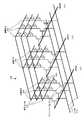
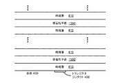
図1は、積層クロスポイントアレイアーキテクチャにおけるプログラム可能なメモリ素子および付随する金属線の平面図を示す。不活性金属の平行線102は第1の層に製作される。固体電解質に対する金属イオン供給源として機能する金属の平行線100は第2の層に製作される。第2の層は、誘電体層(例えば、層間誘電体(ILD))によって第1の層から分離され、平行線100は、平行線102に直角に形成される。線102が線100と交差する各点において、抵抗スイッチング材料が充填されたビア104は2本の線を接続する。各ビア104は、線100および線102において、その上下の金属に沿って延在し、メモリセルを構成する。線102は不活性電極として機能し、線100は金属イオン供給源として機能する。図1に示されるように、線100の層および線102の層を互いに繰り返し積み重ね、線をビア104と連結することによって、三次元メモリアレイが生成される。 FIG. 1 shows a plan view of programmable memory elements and associated metal lines in a stacked crosspoint array architecture. Inert metal parallel lines 102 are fabricated in the first layer. Metal parallel lines 100, which serve as metal ion sources for the solid electrolyte, are fabricated in the second layer. The second layer is separated from the first layer by a dielectric layer (eg, an interlevel dielectric (ILD)), and the parallel lines 100 are formed perpendicular to the parallel lines 102. At each point where the line 102 intersects the line 100, a via 104 filled with resistive switching material connects the two lines. Each via 104 extends along the metal above and below the line 100 and the line 102 to constitute a memory cell. The line 102 functions as an inert electrode, and the line 100 functions as a metal ion supply source. As shown in FIG. 1, a layer of line 100 and a layer of line 102 are repeatedly stacked on top of each other and the lines are connected to vias 104 to create a three-dimensional memory array.
図1のメモリアレイの各層は、少なくとも2つの高分解能のフォトリソグラフィ処理工程、すなわち、ビアをパターン形成する工程および金属線100または102をパターン形成する工程を使用して製作される可能性がある。したがって、N層の積層体は、少なくとも2N+1のフォトリソグラフィマスキング工程を使用して製作されることになり、正しく位置合わせされなければならない。狭い金属線100または102では、高い抵抗にも悩まされ、アレイ内における位置によってはメモリセルの寄生抵抗が高くなる。 Each layer of the memory array of FIG. 1 may be fabricated using at least two high resolution photolithographic processing steps, that is, via patterning and metal line 100 or 102 patterning. . Thus, the N layer stack will be fabricated using at least 2N + 1 photolithographic masking steps and must be properly aligned. Narrow metal lines 100 or 102 also suffer from high resistance, and the parasitic resistance of the memory cell increases depending on the location in the array.
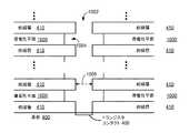
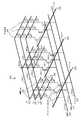
図1のメモリアレイに関連する問題は、絶縁層と交互に配置される水平な導電性平面の積層体を使用する代替のメモリアーキテクチャを使用して緩和することができる。図2は、いくつかの実施形態による、水平な導電性平面202の積層体を用いた三次元メモリアーキテクチャ200の概略図を示す。図2では、視覚的簡略化のため、3つの導電性平面202が示されているが、いくつかの実施形態では、アーキテクチャ200を伴うデバイスは、少なくとも2つの水平な導電性平面202または少なくとも16の水平な導電性平面202または128以上の水平な導電性平面202を備える。アーキテクチャ200は、水平な導電性平面202と直角である垂直な導電性列204のアレイも備える。複数のプログラム可能なメモリ素子206は、三次元アレイ状に配置される。それぞれのプログラム可能なメモリ素子206は、水平な導電性平面202を垂直な導電性列204に連結する。トランジスタ208は、垂直な導電性列204をビット線210に選択的に連結し、これらは順に読み取り回路および書き込み回路(図示せず)に連結される。図2で示されるように、垂直な導電性列204の行(または列)は、それぞれのビット線210に選択的に連結される。選択線212は、トランジスタ208のゲートに連結され、トランジスタ208が垂直な導電性列204をビット線210に選択的に連結することを可能にする。図2で示されるように、トランジスタ208の列(または行)は、それぞれの選択線212に連結される。 The problems associated with the memory array of FIG. 1 can be mitigated using an alternative memory architecture that uses a stack of horizontal conductive planes interleaved with insulating layers. FIG. 2 shows a schematic diagram of a three-
図3A〜3Hおよび4A〜4Hは、いくつかの実施形態による、アーキテクチャ200などの三次元メモリアーキテクチャのさまざまな製作段階を示す。図3A〜3Hは、いくつかの実施形態による、ビット線210(図2)およびトランジスタ208(図2)の製作を示す。 3A-3H and 4A-4H illustrate various stages of fabrication of a three-dimensional memory architecture, such as
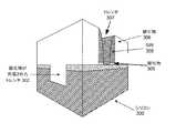
図3Aでは、シリコン300の最上層を組み込み、導電性とする。シリコン300にトレンチ302をエッチングする。トレンチ302には、標準技法を使用してシリコン300に酸化物を堆積させることによって酸化物を充填する。次いで、化学機械研磨(CMP)を行い、トレンチ302の上方または外側にあるすべての酸化物を除去する。いくつかの実施形態では、平行なトレンチ302のセット(図示せず)をシリコン300に形成し、前述のように酸化物で充填する。その結果、導電性のビット線304が製作される。いくつかの実施形態に従って、導電性のビット線304は、ビット線210(図2)として機能する。 In FIG. 3A, the top layer of
図3Bでは、酸化物層306をビット線304および酸化物が充填されたトレンチ302に堆積させ、酸化物層306にトレンチ307をエッチングする。トレンチ307は、垂直トランジスタが製作される開口部を設け、トレンチ307の真下にあるビット線304の一部は、垂直トランジスタのソースとして機能する。酸化物層305(例えば、熱酸化物)をトレンチ307内で成長させる。 In FIG. 3B, an
図3Cでは、窒化ケイ素(SiN)スペーサ(「窒化物スペーサ」)308を酸化物層305(図3B)の上方のトレンチ307の側面に形成し、窒化物スペーサ308で覆われていない酸化物層305の一部をエッチングで除去する。図3Dでは、シリコンを窒化物スペーサ308間の空間内で成長させる(例えば、選択的なエピタキシャル成長を使用)。シリコンの最上層を組み込み、その結果、その真下にチャネル310を備えたドレイン312が形成される。図3Eでは、適切なエッチング(例えば、ウェットエッチングまたはドライエッチング)を使用して窒化物スペーサ308を除去する。それまで窒化物スペーサ308によって占有されていた空間は、垂直トランジスタに対するゲートの製作に使用される。 In FIG. 3C, a silicon nitride (SiN) spacer (“nitride spacer”) 308 is formed on the side of the
図3Fでは、ゲート絶縁体314を、ドレイン312およびチャネル310の上部と側面に形成する。例えば、熱酸化物314を、ドレイン312およびチャネル310の上部と側面で成長させる。チャネル310の側面の熱酸化物314の一部がゲート絶縁体として機能する。 In FIG. 3F, gate insulator 314 is formed on the top and sides of
図3Gに示されるように、ドープされたポリシリコンを堆積させ、異方性エッチバックを行い、それまで窒化物スペーサ308によって占有されていた空間内にドープされたポリシリコンを残留させ、ポリシリコンゲート316を形成する。いくつかの実施形態では、ドープされたポリシリコンをチャネル310の上部の下方でエッチバックを行い、後段の酸化処理後にゲート316が埋設されていること、ならびに、ドレイン312のコンタクトに対して短くならないようにすることを確実にする。熱酸化処理を行い、後段のCMPを妨げる可能性のあるポリシリコンストリンガを低減または除去する(例えば、酸化物406の側壁に沿って)。次いで、酸化物(例えば、低温酸化物)を堆積させ、ドレイン312のエンドポイントでCMPを行い、図3Hの構造体を得る。図3Hでは、チャネル310は、ドレイン312と、ソース318として機能するビット線304の一部との間に垂直に位置する。以下の図4A〜4Hで示されるように、チャネル310、ドレイン312、ソース318、ゲート絶縁体314およびポリシリコンゲート316は、垂直トランジスタを構成し、ビット線304を、垂直トランジスタの上方に製作される垂直な導電性列に選択的に連結する。 As shown in FIG. 3G, doped polysilicon is deposited and an anisotropic etch back is performed to leave the doped polysilicon in the space previously occupied by the
こうして図3A〜3Hは、ビット線210を垂直な導電性列204に連結するトランジスタ208(図2)を製作する方法の例を提供する。図3A〜3Hで示されるように製作されたトランジスタは、ドレイン312、チャネル310およびソース318が垂直に積み重ねられ、チャネル310を通じて流れる電流が実質的に垂直であるため、垂直トランジスタである。しかし、他の実施形態では、トランジスタ208(図2)は、他のタイプのトランジスタとして製作される。例えば、トランジスタ208(図2)は、ソース、チャネルおよびドレインが水平に配置される従来の水平シリコントランジスタとしてまたは薄膜トランジスタ(TFT)として製作することができる。さらに、図3A〜3Hでは、ビット線304は、ドープされたシリコンである。しかし、他の実施形態では、ビット線210(図2)は、例えば、ドープされたポリシリコンまたは金属を使用して実装される。 3A-3H thus provide an example of how to fabricate transistor 208 (FIG. 2) that couples bit line 210 to vertical
図4A〜4Hは、いくつかの実施形態による、基板の上方の三次元メモリアレイの製作を示す。図4A〜4Hは固体電解質抵抗スイッチング材料を使用するプログラム可能なメモリ素子のアレイを製作するためのプロセスを示すが、類似したプロセスを使用して、他のタイプの抵抗スイッチング材料を使用するプログラム可能なメモリ素子のアレイを製作してもよい。 4A-4H illustrate the fabrication of a three-dimensional memory array over a substrate, according to some embodiments. 4A-4H illustrate a process for fabricating an array of programmable memory elements using solid electrolyte resistive switching materials, but using a similar process, programmable using other types of resistive switching materials An array of memory elements may be fabricated.
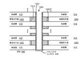
図4Aは、いくつかの実施形態による平面基板400を示し、その上には、交互に位置する水平な絶縁層と導電性平面を製作する。本明細書で使用される用語「基板」は、単にバルクシリコンまたは他の半導体材料(例えば、シリコン300、図3A〜3H)ばかりではなく、バルクシリコン上に製作される1つまたは複数の層(例えば、1つまたは複数のポリシリコンおよび/または金属層)も含み、したがって、パターン形成、堆積または他の処理の対象であった1つまたは複数の層を含むことができる。基板は、その上に製作される、交互に位置する水平な絶縁層と導電性平面を支持する。基板400は、ビット線210(図2)として機能する複数の平行な信号線/ビット線402を備える。いくつかの実施形態では、信号線/ビット線402は、ドープされたシリコンにおいて製作される(例えば、ビット線304、図3A〜3H)。あるいは、ビット線402は、ドープされたポリシリコンまたは金属を使用して製作される。基板400は、選択線212(図2)の一例である複数の平行な選択線404や、対応するトランジスタ208(図2;図4Aではトランジスタは視覚的簡略化のために示されていない)に接触するトランジスタコンタクト406のアレイも備える。垂直な導電性列は、それぞれのトランジスタコンタクト406の上方に製作される。いくつかの実施形態では、それぞれのトランジスタコンタクト406は、垂直トランジスタのドレイン(例えば、ドレイン312、図3H)である。あるいは、それぞれのトランジスタコンタクト406は、それぞれのビット線402を垂直な導電性列に選択的に連結するよう構成される別のタイプのトランジスタ(例えば、従来の水平シリコントランジスタまたはTFT)のソースまたはドレインに連結する。こうして、それぞれのビット線402は、複数のトランジスタによって、基板400において行(または列)をなして配置された複数のトランジスタコンタクト406に選択的に連結するよう構成される。それぞれの選択線404は、コンタクト406の列(または行)に連結されたトランジスタのゲートに連結し、トランジスタがビット線402をコンタクト406に選択的に連結することを可能にする。いくつかの実施形態では、選択線404は、ドープされたポリシリコンまたはその代わりの金属である。 FIG. 4A illustrates a
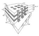
図4Bでは、交互に位置する水平な絶縁層410と導電性平面412を、公知の技法を使用して基板400の上方に堆積させる。こうして、層410および412が交互に配置され、それぞれの絶縁層410は、連続的な導電性平面412を分離するILDを形成する。導電性平面412は、導電性平面202(図2)の例である。図4Bでは、簡略化のため、2つの導電性平面412が示されているが、いくつかの実施形態では、メモリデバイスは、少なくとも2つの水平な導電性平面412または少なくとも16の水平な導電性平面412または128の水平な導電性平面412またはそれ以上を備える。導電性平面412はパターン形成されるが、そのサイズは、最小のフォトリソグラフィフィーチャサイズと比べて大きく、その結果、最小またはほぼ最小のフォトリソグラフィフィーチャサイズを伴うフォトリソグラフィマスキング工程は、連続的な平面410および412の堆積間では行わない。通常、それぞれの絶縁層410の堆積後に、CMP工程を行い、平面性を確保する。いくつかの実施形態では、それぞれの導電性平面412および/または絶縁層410は、およそ50nmの厚さを有する。 In FIG. 4B, alternating horizontal insulating
いくつかの実施形態では、各絶縁層410は、二酸化ケイ素(SiO2)を含むか、またはその代わりに、合理的な選択性でフォトレジストに異方的にエッチングを施すことができる低k誘電体を含む。いくつかの実施形態では、各導電性平面412は、不活性金属(例えば、白金、Pt)の層を含む複数の金属層の積層体(例えば、Ti−Pt−Ti積層体)である。In some embodiments, each insulating
図4Cでは、フォトレジスト層414を、絶縁層410と導電性平面412の積層体に堆積させ、フォトリソグラフィによってパターン形成してビア416のアレイを形成する。いくつかの実施形態では、ビア416は、最小の利用可能なフォトリソグラフィの線幅(例えば、メモリを製作する製造工場で利用可能な最高分解能のフォトリソグラフィツールによって提供される最小のフィーチャサイズ)に対応する直径およびピッチを有する。例えば、ビア416の直径およびピッチは、45ナノメートル(nm)、または32nm、または25nm、または20nmでよい。いくつかの実施形態では、このパターンは、積層体とレジスト414との間の「ハードマスク」材料に移行される。例えば、導電性平面412におけるチタン(Ti)層をハードマスクとして使用してもよい。次いで、ビア416に、交互に位置する水平な絶縁層410と導電性平面412を貫通する形でエッチングを施す。導電性平面412がTi−Pt−Ti積層体であるいくつかの実施形態では、チタン膜には、フッ素化学(例えば、CHF3/O2またはSF6)でドライエッチングを施し、白金には、CO/NH3/Xeでエッチングを施す。最終の絶縁体エッチングは、シリコンに関して良好な選択性を呈し、コンタクト406がドープされたシリコンである実施形態に対してコンタクト406(図4A)で停止するエッチングを可能にする。図4Dは、得られた構造体の切断図を示す。この切断図では、ビア416の側壁418を見ることができる。図4Eに示されるように、レジスト414は剥ぎ取られる。In FIG. 4C, a
図4Fでは、抵抗スイッチング材料420を、ビア416の側壁418(図4E)に共形に堆積させる。いくつかの実施形態では、抵抗スイッチング材料420は、CuがドープされたSiO2または純粋なSiO2である。エッチングを施し、ビア416の底部でコンタクト406(図4A)を開口する。次いで、図4Gで示されるように、金属422(例えば、銅、Cu)を、ビア416に共形に堆積させ(例えば、原子層堆積法(ALD)を使用)、ビア416を充填する。各ビア416における金属422は、垂直な導電性列(例えば、列204、図2)を構成する。特定のビア416における抵抗スイッチング材料420および金属422と導電性平面412との各交差点は、プログラム可能なメモリ素子またはメモリセルであり、これは導電性平面412をそのビア416に対応する垂直な導電性列に連結する。抵抗スイッチング材料420および金属422で充填されたビア416は、絶縁層410および導電性平面412において開口部を効果的に形成する。抵抗スイッチング材料420および金属422によって形成された垂直な導電性列は、これらの開口部を通過する。In FIG. 4F,
こうして、図4A〜4Gでは、プログラム可能なメモリ素子のアレイは、単一のフォトリソグラフィマスキング工程を使用して形成されるが、その理由は、ビア416が1つのマスキング工程で画定されるためである。こうして、この設計は、多くのマスキング工程を必要とする設計と比較して重要な利益を提示する。 Thus, in FIGS. 4A-4G, the array of programmable memory elements is formed using a single photolithographic masking process because the
図4A〜4Gで示された構造体のいくつかの実施形態では、導電性平面412は、白金などの不活性金属を含む。特定のビア416を囲む導電性平面412の領域は、それぞれのプログラム可能なメモリ素子の不活性電極として機能する。しかし、不活性金属の処理は、重要な課題および費用を提示する。例えば、不活性金属はエッチングするのが難しい。したがって、いくつかの実施形態では、導電性平面412はドープされたポリシリコンであり、不活性電極はガルバニック置換(「GD」)として知られているプロセスを使用して製作される。導電性平面412に対するポリシリコンの使用により、従来の反応性イオンエッチング(RIE)化学を使用してビア416にエッチングを施すことが可能になる。これらの従来のRIE化学は、高アスペクト比のビアの生成が可能な標準の製造工場ツールを使用して実施される。 In some embodiments of the structure shown in FIGS. 4A-4G, the
導電性平面412がポリシリコンであるため、ビア416を開口するエッチングにより、導電性平面412がビア416と交差する各点において、側壁418に沿ってポリシリコン表面が露出する。GDプロセスを行うため、側壁418は、後に堆積するフッ化水素酸(HF)および金属塩(例えば、不活性金属)を含有する水溶液電解槽に曝される。槽内の金属イオンは、側壁418に沿って露出したポリシリコン表面の酸化によって還元され、露出したポリシリコンへの金属膜の選択的な自己制限堆積が生じる。こうして、金属は、側壁418に沿って、露出したポリシリコンに堆積するが、露出した絶縁体には堆積しない。図4Hは、白金430を堆積させるためにHFおよびヘキサクロロ白金酸塩の溶液を使用してGDプロセスを行った結果の予測例を示す。いくつかの実施形態では、図4H(例えば、ガルバニック置換による不活性金属の堆積を表す)は、図4E(ビア416のエッチングを表す)の後段であり、図4F(すなわち、ビア416の側壁418に沿って抵抗スイッチング材料420の堆積前)の前段である。図4Hで示されるように、白金430は、ポリシリコンの導電性平面412がビア416と交差する側壁の部分に堆積しているが、絶縁層410がビア416と交差する側壁418の部分には堆積していない。次いで、図4F〜4Gに関して上述したように、抵抗スイッチング材料420および金属422をビア416に堆積させる。GDによって堆積させた白金430は、得られたプログラム可能なメモリ素子において、不活性電極として機能する。GDによって堆積させ、不活性電極として機能することができる他の不活性金属の例として、TiWおよびTiNが挙げられる。 Since the
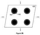
図5A〜5Dは、図4A〜4Hに従って製作されたプログラム可能なメモリ素子の断面図および平面図をそれぞれ示す。図5A〜5Bは、いくつかの実施形態による、メモリアレイの一部の断面図および平面図をそれぞれ示し、導電性平面412は、アレイにおいてプログラム可能なメモリ素子の不活性電極として機能する不活性金属(例えば、Pt)を含む。導電性平面412は、抵抗スイッチング材料420(例えば、純粋なSiO2またはCuがドープされたSiO2)をビア416の外側に沿って、金属422(例えば、Cu)をビア416の内側に沿って堆積させたビア416と交差する。抵抗スイッチング材料420は、片側が導電性平面412の不活性金属に接触し、反対側が金属422に接触し、こうして、RRAMのプログラム可能なメモリ素子を作成する。抵抗スイッチング材料420のリングは、金属422に対して同心円状に配置される。図5Bの平面図は、アレイにおけるそのような4つのプログラム可能なメモリ素子を示す。抵抗スイッチング材料420の抵抗特性のため、同列の金属422に連結されたメモリ素子は、互いに電気的に絶縁される。5A-5D show a cross-sectional view and a top view, respectively, of a programmable memory device fabricated according to FIGS. 4A-4H. 5A-5B show a cross-sectional view and a top view, respectively, of a portion of a memory array, according to some embodiments, where the
特定のプログラム可能なメモリ素子のための抵抗スイッチング材料420および金属422の組合せは、導電性平面412の開口部を構成する。抵抗スイッチング材料420は開口部の第1の部分に位置し、金属422は開口部の第2の部分に位置する。図5Bでは、開口部の第1の部分は完全なリングとして示されているが、それに限定されない。例えば、抵抗スイッチング材料420は、金属422の周りに部分的なリングまたは他の適切な形状を形成することも可能である。 The combination of
図5C〜5Dは、いくつかの実施形態による、メモリアレイの一部の断面図および平面図をそれぞれ示し、導電性平面412は、ドープされたポリシリコンである。図4Hに関して上述したように、白金(または他の不活性金属、例えば、TiWまたはTiN)のリング430は、GDプロセスを使用して、導電性平面412とビア416との各交差点の周りに製作されている。それぞれの白金のリング430は、抵抗スイッチング材料420のリングに接触し、抵抗スイッチング材料420のリングに対して同心円状であり、抵抗スイッチング材料420は、金属422に接触し、金属422に対して同心円状に配置され、こうして、プログラム可能なメモリ素子を形成する。図5Dでは、リング420および422は完全なリングとして示されているが、それに限定されない。例えば、白金430および/または抵抗スイッチング材料420は、金属422の周りに部分的なリングまたは他の適切な形状を形成することも可能である。 5C-5D show a cross-sectional view and a top view, respectively, of a portion of a memory array, according to some embodiments, where the
図6は、いくつかの実施形態による、三次元メモリアレイの製作方法600を示すフロー図である。例えば、方法600を使用して、図2のアーキテクチャ200を用いてメモリアレイを製作する。図3A〜3Hおよび4A〜4Hは、方法600のさまざまな段階での三次元メモリアレイの素子および付随する回路の例を示す。 FIG. 6 is a flow diagram illustrating a
方法600では、平面基板(例えば、シリコン300、図3A;基板400、図4A)において、複数の平行な信号線(例えば、ビット線304、図3A;ビット線402、図4A)を製作する(602)。複数のトランジスタ(例えば、図3Hで示される、ソース318、ドレイン312、チャネル310およびゲート316を備える垂直トランジスタまたはその代わりのTFTもしくは従来の水平シリコントランジスタ)を製作し、それぞれの信号線を、後段の作業で製作されるそれぞれの垂直な導電性列に連結する。それぞれのトランジスタセットのゲートに連結する選択線(例えば、選択線404、図4A)を製作する。 In the
平面基板の上方に、複数の交互に位置する絶縁平面(例えば、絶縁層410、図4B)と導電性平面(例えば、導電性平面412、図4B)を製作する(604)。いくつかの実施形態では、それぞれの導電性平面は、不活性金属を含む。いくつかの実施形態では、それぞれの導電性平面は、ドープされたポリシリコンを含む。 A plurality of alternating insulating planes (eg, insulating
いくつかのこれらの実施形態では、それぞれの導電性平面は、導体が積み重なった積層体を含む。例えば、各導電性層は、隣接する絶縁平面に接面する金属層間に位置する不活性金属層(例えば、Ti−Pt−Ti積層体)を含む。 In some of these embodiments, each conductive plane includes a stack of stacked conductors. For example, each conductive layer includes an inert metal layer (eg, a Ti—Pt—Ti stack) located between metal layers that are in contact with adjacent insulating planes.
複数の交互に位置する導電性平面および絶縁平面を貫通する形で複数のビア(例えば、416、図4C〜4E)にエッチングを施す(606)。 Etching is performed on a plurality of vias (eg, 416, FIGS. 4C-4E) through a plurality of alternating conductive and insulating planes (606).
いくつかの実施形態では、ガルバニック置換を使用して、金属(例えば、不活性金属、例えば、白金430(図4H)、TiWまたはTiN)を、ビアの側壁で露出したポリシリコンに堆積させる(608)。 In some embodiments, galvanic substitution is used to deposit a metal (eg, an inert metal, eg, platinum 430 (FIG. 4H), TiW, or TiN) on polysilicon exposed at the via sidewalls (608). ).
抵抗スイッチング材料(例えば、材料420、図4F)をビアの側壁(例えば、側壁418、図4E)に共形に堆積させる(610)。いくつかの実施形態では、抵抗スイッチング材料はSiO2を含み、SiO2は、本質的なものまたはドープされたもの(例えば、Cuがドープされたもの)でよい。あるいは、抵抗スイッチング材料は、GeSe、GeSまたはCuOを含む。Resistive switching material (eg,
金属(例えば、金属422、図4G)をビアに堆積させ、抵抗スイッチング材料に電気コンタクトを設ける(612)。堆積させた金属は、垂直な導電性列を形成する。例えば(例えば、抵抗スイッチング材料がSiO2、GeSe、GeSまたはCuOを含むいくつかの実施形態)、抵抗スイッチング材料にCu膜を共形に堆積させる(614)。別の例(例えば、抵抗スイッチング材料がGeSeを含むいくつかの実施形態)では、堆積させた金属は銀を含む。いくつかの実施形態(例えば、抵抗スイッチング材料がSiO2である)では、ポリシリコンをビアに共形に堆積させ、ガルバニック置換を使用してポリシリコンを金属に置き換える(616)。A metal (eg,
こうして、方法600は、三次元メモリアレイ(例えば、図2のアーキテクチャ200を用いたアレイ)を製作するための効果的なプロセスを実現する。ビアおよびプログラム可能なメモリ素子の形成には、単一のマスキング工程(例えば、最小またはほぼ最小のフォトリソグラフィフィーチャサイズを伴う単一のマスキング工程)のみが必要とされる。追加のマスキング工程を実施して導電性平面をパターン形成することも可能だが、これらの追加のマスキング工程には、最小またはほぼ最小のフォトリソグラフィフィーチャサイズは伴わない。 Thus, the
RRAMメモリアレイ(例えば、プログラム可能なメモリ素子206が抵抗スイッチング材料を備えるアーキテクチャ200を用いたアレイ)に関連する一課題は、寄生漏れ経路の存在である。例えば、図7Aは、いくつかの実施形態による、三次元RRAMアレイ700の概略縦断面図を示す。アレイ700では、複数の平行な水平な導電性平面702−0〜702−3は、複数の垂直な導電性列704−0および704−1と交差する。RRAMセル706は、平面702と列704のそれぞれの交差点に位置する。一シナリオでは、平面702−1と列704−0の交差点のセル706−0は高抵抗状態であり、他のセル706は低抵抗状態である。平面702−1をオンにすると、列704−0が選択され、他の平面702および列704は高インピーダンス状態となり、寄生漏れ経路が、例えば、低抵抗状態においてセル706−1、706−2および706−3を通して作成される可能性がある。 One challenge associated with RRAM memory arrays (eg, an
寄生漏れ経路の影響は、それぞれのRRAMセルにおいて(すなわち、それぞれのプログラム可能なメモリ素子において)、抵抗スイッチング材料と直列に絶縁デバイスを備え、それぞれのRRAMセルを通して寄生漏れ電流の導通を低減または抑制することによって、低減することができる。図7Bは、いくつかの実施形態による、三次元RRAMアレイ710の概略縦断面図を示し、それぞれのプログラム可能なメモリ素子712は、抵抗スイッチング材料714と直列に絶縁デバイス716を備える。絶縁デバイス716は、並列だが逆向きに配線される2つのダイオードとして実装される。この構成により、絶縁デバイス716は双方向に導通するが、それは、絶縁デバイス716の両端間電圧の大きさが、ダイオードドロップに相当する閾値電圧VTHを超える場合のみに該当する。絶縁デバイス716の双方向導電性により、操作中に正と負の両方の電圧が抵抗スイッチング材料714に印加されるプログラム可能なメモリ素子712において、絶縁デバイス716を使用することが可能になる。アレイ710では、寄生漏れ経路は複数の絶縁デバイス716を直列に通過し、アレイ700(図7A)での類似した寄生漏れ経路と比較して、電流を数桁減少させる。あるいは、閾値電圧VTH(例えば、ダイオード)を超えると一方向導電性を有する絶縁デバイスは、単極性のプログラム可能なメモリ素子において、抵抗スイッチング材料と直列に位置する。The effects of parasitic leakage paths include an isolation device in series with the resistive switching material in each RRAM cell (ie, in each programmable memory element) to reduce or suppress conduction of parasitic leakage currents through each RRAM cell. This can be reduced. FIG. 7B shows a schematic longitudinal cross-sectional view of a three-
いくつかの実施形態では、逆向きの並列ダイオードを使用して絶縁デバイス716を実装する代わりに、閾値電圧VTHを超えると双方向導電性を有する絶縁デバイスが、逆向きの並列ダイオードのI−V特性と等しいI−V特性を有する別の物理的構造体として実装される。例えば、絶縁デバイスに、2つの導体間に位置する誘電体材料または絶縁体を備えて、2つの導体が誘電体材料によって連結される金属・絶縁体・金属(MIM)構造体をもたらすことも可能である。こうして、2つの導体それぞれがMIM構造体の電極として機能し、絶縁デバイスとして機能する。図8は、いくつかの実施形態による、プログラム可能なメモリ素子800(すなわち、メモリセル800)を示し、MIM構造体は、抵抗スイッチング材料808と直列に存在し、抵抗スイッチング材料808とは異なる絶縁デバイスを形成する。プログラム可能なメモリ素子800は、いくつかの実施形態による、プログラム可能なメモリ素子206(図2)の一例である。プログラム可能なメモリ素子800は、いくつかの実施形態による、メモリアーキテクチャ200(図2)などの三次元アレイ状に配置してもよい。In some embodiments, instead of using an inverted parallel diode to implement the isolation device 716, an isolation device that has bidirectional conductivity above the threshold voltage VTH may be coupled to the reverse parallel diode I- It is implemented as another physical structure having an IV characteristic equal to the V characteristic. For example, an insulating device can be provided with a dielectric material or insulator located between two conductors, resulting in a metal-insulator-metal (MIM) structure in which the two conductors are connected by a dielectric material It is. Thus, each of the two conductors functions as an electrode of the MIM structure and functions as an insulating device. FIG. 8 illustrates a programmable memory element 800 (ie, memory cell 800) according to some embodiments, where the MIM structure is in series with the resistive switching material 808 and is different from the resistive switching material 808. Form the device.
プログラム可能なメモリ素子800では、水平な導電性平面802は、MIM構造体の第1の導体を形成する。導電性平面802の開口部に位置する絶縁膜804および金属層806の同心円状のリングはそれぞれ、MIM構造体の絶縁体および第2の導体を形成する。いくつかの実施形態では、絶縁膜804は、20Å未満またはわずか10Åの厚さを有する。金属層806は、開口部における絶縁膜804および金属806のリングと同心円状の抵抗スイッチング材料808のリングに対する第1の電極としても機能する。金属810は、開口部を通過する垂直な導電性列を形成し、抵抗スイッチング材料808のリングに対する第2の電極として機能する。図8では、絶縁膜804、金属層806および抵抗スイッチング材料808は同心円状のリングとして示されているが、それに限定されない。より一般的には、絶縁膜804、金属層806および抵抗スイッチング材料808はそれぞれ、MIM構造体が抵抗スイッチング材料808と直列に存在するように、導電性平面802の開口部のそれぞれの部分を占有する。 In the
図9は、いくつかの実施形態による、MIM構造体のI−V特性900−1および900−2の例を示す。例えば、I−V特性900−1および900−2は、いくつかの実施形態による、導電性平面802、絶縁膜804および金属806(図8)によって形成されたMIM構造体に対応する。I−V特性900−1は、閾値電圧VTH902−1を超えると双方向導電性を示す。MIM構造体の両端間電圧が負であるか正であるかに関わらず、MIM構造体の両端間電圧の大きさがVTH902−1を超える場合に対応するMIM構造体が導通するため、導電性は双方向である。同様に、I−V特性900−2は、閾値電圧VTH902−2を超えると双方向導電性を示す。いくつかの実施形態では、I−V特性900−1および900−2は、同じ構造体に相当し、I−V特性900−1と900−2との違いは、処理の違いにより生じる。例えば、I−V特性900−2に相当するMIM構造体は、I−V特性900−1に相当する類似したMIM構造体よりも高い温度でアニール処理が施された可能性がある。I−V特性900−1および900−2はVTH902−1および902−2を超えると対称的な双方向コンダクタンスを示すが、双方向コンダクタンスは対称的である必要はない。FIG. 9 illustrates examples of IV characteristics 900-1 and 900-2 of MIM structures, according to some embodiments. For example, the IV characteristics 900-1 and 900-2 correspond to an MIM structure formed by the
図10A〜10Fは、いくつかの実施形態による、製作の連続段階でのプログラム可能なメモリ素子800(図8)のアレイの断面図を示す。図10Aでは、交互に位置する水平な絶縁平面410および導電性平面1000を、基板400(図4A)の上方に堆積させている。いくつかの実装形態では、導電性平面1000はアルミニウムである。いくつかの実施形態では、それぞれの導電性平面1000および/または絶縁層410は、およそ50nmの厚さを有する。 10A-10F show cross-sectional views of an array of programmable memory elements 800 (FIG. 8) in successive stages of fabrication, according to some embodiments. In FIG. 10A, alternating horizontal insulating
図10Bでは、ビア1002に、絶縁平面410と導電性平面1000を貫通する形でエッチングを施す。いくつかの実施形態では、ビア1002は、0.2ミクロンの直径1005を有する。ビア1002は、トランジスタコンタクト406(図4A)で終止する。ビア1002を形成するエッチングにより、ビア1002の側壁に沿って露出するにつれて導電性平面1000にアンダーカットを入れ、側壁に沿って凹部1004を形成する。 In FIG. 10B, the via 1002 is etched through the insulating
図10Cでは、絶縁体1006を凹部1004に形成する。絶縁体1006は、開口ビア1002から導電性平面1000を分離する。いくつかの実施形態では、導電性平面1000がアルミニウムの場合は、絶縁体1006は、凹部1004で露出しているアルミニウムに陽極酸化処理を施してAl2O3(サファイア)を形成することによって製作される。絶縁体1006は絶縁体804(図8)の一例である。In FIG. 10C, the
図10Dでは、凹部1004は、ビア1002にポリシリコン(「ポリ−Si」)1008を共形に堆積させ、次いで、エッチングを施し、ビア1002の側面および底部からポリ−Siを除去し、凹部1004にのみポリ−Siを残留させることによって、ポリ−Siで充填している。次いで、図10Eで示されるように、ガルバニック置換を行い、ポリ−Si1008を金属1010(例えば、不活性金属、例えば、Pt、TiWまたはTiN)と置き換える。金属1010は金属806(図8)の一例である。 In FIG. 10D,
あるいは、ポリ−Si1008の堆積を省略し、ビア1002に金属1010を共形に堆積させ、次いで、エッチングを施して凹部1004以外の金属1010を除去する。 Alternatively, deposition of poly-
図10Fで示されるように、抵抗スイッチング材料1012(例えば、純粋またはCuがドープされたSiO2)をビア1012の側壁に共形に堆積させる。抵抗スイッチング材料1012は抵抗スイッチング材料808(図8)の一例である。次いで、図10Gで示されるように、ビア1002を金属1014(例えば、Cu)で充填し、それぞれのトランジスタコンタクト406に接続する垂直な導電性列を形成する。金属1014は金属810(図8)の一例である。こうして、図10A〜10Gは、導電性平面1000とビア1002との各交差点におけるプログラム可能なメモリ素子800(図8)の形成を示す。導電性平面1002、絶縁体1006および金属1010は、絶縁デバイスとして機能するMIM構造体および抵抗スイッチング材料1012と直列に存在するMIM構造体を形成する。金属1010は、絶縁デバイスおよび抵抗スイッチング材料1012の両方に共通の電極である。As shown in FIG. 10F, a resistive switching material 1012 (eg, pure or Cu doped SiO2 ) is conformally deposited on the sidewalls of the via 1012.
図11は、いくつかの実施形態による、三次元メモリアレイの製作方法1100を示すフロー図である。例えば、方法1100を使用して、図2のアーキテクチャ200を用いてメモリアレイを製作し、これは、閾値電圧を超えると双方向コンダクタンスを有する絶縁デバイスと直列に抵抗スイッチング材料を備える、プログラム可能なメモリ素子206(例えば、プログラム可能なメモリ素子800、図8)を備える。図10A〜10Gは、方法1100のさまざまな段階での、そのような三次元メモリアレイの素子の例を示す。 FIG. 11 is a flow diagram illustrating a
方法1100では、平面基板において、複数の平行な信号線を製作する(602)。複数のトランジスタを製作し、それぞれの信号線を、後段の作業で製作されるそれぞれの垂直な導電性列に連結する。それぞれのトランジスタセットのゲートに連結する選択線を製作する。作業602は、方法600(図6)に対して説明されるように行う。 In
平面基板(例えば、基板400、図10A)の上方に、複数の交互に位置する絶縁平面と導電性平面(例えば、絶縁層410と導電性平面1000、図10A)を製作する(604)。いくつかの実施形態では、導電性平面は、アルミニウムを使用して製作する(1106)。 A plurality of alternating insulating and conductive planes (eg, insulating
複数の交互に位置する導電性平面および絶縁平面を貫通する形で複数のビア(例えば、ビア1002、図10B)にエッチングを施す(1108)。ビアの側壁に沿って導電性平面にアンダーカットを入れ、側壁に沿って凹部(例えば、凹部1004、図10B)を形成する。 Etching is performed on a plurality of vias (eg, via 1002, FIG. 10B) through a plurality of alternating conductive and insulating planes (1108). An undercut is made in the conductive plane along the side wall of the via to form a recess (eg,
絶縁体(例えば、絶縁体1006、図10C)を凹部に形成する(1110)。導電性平面がアルミニウムであるいくつかの実施形態では、凹部で露出しているアルミニウムに陽極酸化処理を施してAl2O3を形成する(1112)。An insulator (eg,
金属を凹部の絶縁体に堆積させる(1114)。いくつかの実施形態では、ガルバニック置換を使用して金属を堆積させる。ビアの側壁に沿って凹部にポリ−Si(例えば、ポリ−Si1008、図10D)を堆積させ、GDを行い、ポリ−Siを金属(例えば、金属1010、図10E)(例えば、不活性金属、例えば、Pt、TiWまたはTiN)と置き換える。あるいは、ビアの側壁に沿って金属を共形に堆積させ、次いで、エッチングを施して凹部以外の金属を除去する。 Metal is deposited on the insulator in the recess (1114). In some embodiments, galvanic substitution is used to deposit the metal. Poly-Si (eg, poly-
抵抗スイッチング材料(例えば、抵抗スイッチング材料1012、図10F)をビアの側壁に共形に堆積させる(1116)。ビアに金属(例えば、金属1014、図10G)を堆積させ、抵抗スイッチング材料に電気コンタクトを設ける(1118)。堆積させた金属は垂直な導電性列を形成する。 Resistive switching material (eg,
こうして、方法1100は、三次元メモリアレイを製作するための効果的なプロセスを実現する。ビアおよびプログラム可能なメモリ素子の形成には、単一のマスキング工程のみが必要とされる。いくつかの実施形態では、GDにより、不活性金属にエッチングを施す必要なしに不活性金属を堆積させることができる。 Thus, the
ここで、メモリアーキテクチャ200(図2)におけるRRAMのプログラム可能なメモリ素子(すなわち、RRAMセル)の読み取りおよび書き込みに注目する。RRAMセルに書き込む(すなわち、プログラミング)ための操作タイプは、相変化メモリのための単極性パルス形成、双極性パルス形成および時間依存性パルス形成を含む。メモリアーキテクチャ200(図2)におけるRRAMセルは、例えば、単極性もしくは双極性のいずれかであってよく、または、相変化メモリであってもよい。一般に、RRAMを絶縁するのは単極性である。一般に、固体電解質RRAMは双極性であり、単極性モードで操作できる場合もある。双極性デバイスは、典型的に、何らかの物理的な非対称性、例えば、異なる材料からなる電極を有する。RRAMセルにおける低抵抗状態の作出は「SET」操作と呼ばれ、RRAMセルにおける高抵抗状態の作出は「RESET」操作と呼ばれる。 Attention is now directed to reading and writing RRAM programmable memory elements (ie, RRAM cells) in memory architecture 200 (FIG. 2). Operation types for writing (ie, programming) to RRAM cells include unipolar pulse formation, bipolar pulse formation and time-dependent pulse formation for phase change memory. The RRAM cell in memory architecture 200 (FIG. 2) may be, for example, either unipolar or bipolar, or may be a phase change memory. In general, it is unipolar that insulates the RRAM. In general, the solid electrolyte RRAM is bipolar and may be operable in a unipolar mode. Bipolar devices typically have some physical asymmetry, eg, electrodes made of different materials. Creation of a low resistance state in an RRAM cell is referred to as a “SET” operation, and creation of a high resistance state in an RRAM cell is referred to as a “RESET” operation.
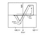
図12Aは、いくつかの実施形態による、単極性RRAMセル(例えば、単極性RRAMのプログラム可能なメモリ素子206、図2)に対する電流対電圧曲線を示す。単極性セルの場合、RESET操作1206に対して示されているように、セルに印加されるパルスの電圧がRESET電圧VR1202以上であり、SET電圧VS1204未満であれば、高抵抗状態が作出される。SET操作1208に対して示されているように、セルに印加されるパルスの電圧がSET電圧VS1204以上であれば、低抵抗状態が作出される。FIG. 12A shows a current versus voltage curve for a unipolar RRAM cell (eg, unipolar RRAM
図12Bは、いくつかの実施形態による、双極性RRAMセル(例えば、双極性RRAMのプログラム可能なメモリ素子206、図2)に対する電流対電圧曲線を示す。双極性セルの抵抗スイッチング材料は双方向性とされる。双極性セルの場合、RESET操作において印加される電圧の極性は、SET操作において印加される電圧の極性と反対である。RESET操作1216に対して示されているように、セルに印加されるパルスの電圧が第1の極性(図12Bでは、負として示される)を有し、その大きさがRESET電圧VR1212以上であれば、高抵抗状態が作出される。SET操作1218に対して示されているように、セルに印加されるパルスの電圧が第1の極性とは反対の第2の極性(図12Bでは、正として示される)を有し、その大きさがSET電圧VS1214以上であれば、低抵抗状態が作出される。FIG. 12B illustrates a current versus voltage curve for a bipolar RRAM cell (eg, bipolar RRAM
相変化メモリ素子の時間依存性パルス形成の場合、SET操作は、印加された電流パルスを素早く消滅させることによって実行され、RESET操作は、印加された電流パルスを徐々に減少させることによって実行される。電流パルスは、抵抗素子材料の融解に使用される。この電流パルスが素早く消滅されれば、材料は急速に冷却され、低導電性を有する非晶質状態に材料をクエンチする。電流を時間とともに徐々に減少させれば、材料は高導電性を有する結晶構造を形成する。 For time-dependent pulse formation of phase change memory elements, the SET operation is performed by quickly extinguishing the applied current pulse, and the RESET operation is performed by gradually decreasing the applied current pulse. . The current pulse is used to melt the resistive element material. If this current pulse is quickly extinguished, the material cools rapidly, quenching the material into an amorphous state with low conductivity. If the current is gradually reduced over time, the material forms a crystalline structure with high conductivity.
導電性平面202と垂直な導電性列204との交差点に位置する、単一のプログラム可能なメモリ素子206(図2)に対するSETおよびRESET操作は、導電性平面202と、垂直な導電性列204に連結されるビット線210との間に電圧を印加することによって実行される。ビット線210は、選択線212に電圧を印加して、垂直な導電性列204に連結されるトランジスタ208を含むトランジスタ208をオンにすることによって、垂直な導電性列204に連結される。特定のSETまたはRESET操作に関与しない導電性平面204は、高インピーダンス「Z」状態(すなわち、トライステート状態である)に保持し、選択線212によって選択された列204に付随するこれらの平面における素子206の意図せぬプログラミングを防ぐ。SETおよびRESET操作の両方に対してそれぞれのプログラム可能なメモリ素子206を個別に割り当てることが可能なため、別々の消去操作は不要である。 SET and RESET operations on a single programmable memory element 206 (FIG. 2), located at the intersection of the
図13Aは、いくつかの実施形態による、メモリアーキテクチャ200における、単極性のプログラム可能なメモリ素子206のSETおよびRESET操作を示す。具体的には、図13Aは、プログラム可能なメモリ素子206−1および206−2に対して同時に行われるSET操作、ならびに、プログラム可能なメモリ素子206−0に対するRESET操作を示す。導電性平面202−1は平面202−1を接地する(GND222)ことによって選択されるが、他の導電性平面202−0および202−2はトライステート状態(「Z」220)であるため非選択状態である。行をなして配置された垂直な導電性列204−0、204−1および204−2は、論理レベルH(「1」230)に相当する電圧を選択線212−1に印加することによって選択され、それにより、トランジスタ208−0、208−1および208−2をオンにする。トランジスタ208−0、208−1および208−2をオンにすることにより、垂直な導電性列204−0、204−1および204−2がそれぞれのビット線210−0、210−1および210−2に連結される。他の行の垂直な導電性列204は、論理レベルL(「0」228)に相当する電圧(例えば、GND)を選択線212−0および212−2に印加することによって示されるように、非選択状態のままである。ゲートが選択線212−0および212−2に連結される対応するトランジスタ208は、オフ状態のままであり、したがって、それらの対応する列204をビット線210に連結しない。SET電圧VS224が同時にビット線210−1および210−2に印加され、それにより、素子206−1および206−2に印加され、素子206−1および206−2において低抵抗状態が作出される。同時に、RESET電圧VR226がビット線210−0に印加され、それにより、素子206−0に印加され、素子206−0において高抵抗状態が作出される。低抵抗状態が論理レベルL(「0」)と見なされ、高抵抗状態が論理レベルH(「1」)と見なされる場合、図13Aは、単極性素子206−0、206−1および206−2への書き込み「100」を示す。FIG. 13A illustrates SET and RESET operations of a unipolar
図13Bは、いくつかの実施形態による、メモリアーキテクチャ200における、双極性のプログラム可能なメモリ素子206のSETおよびRESET操作を示す。具体的には、図13Bは、プログラム可能なメモリ素子206−1および206−2に対して同時に行われるSET操作、ならびに、プログラム可能なメモリ素子206−0に対するRESET操作を示す。導電性平面202−1はSET電圧VS234を平面202−1に印加することによって選択されるが、他の導電性平面202−0および202−2はトライステート状態(「Z」220)であるため非選択状態である。垂直な導電性列204−0、204−1および204−2は、図13Aに関して論じられたように選択される。ビット線210−1および210−2は接地(GND222)され、その結果、SET電圧VS234が素子206−1および206−2に印加される。こうして、素子206−1および206−2は、低抵抗状態にプログラミングされる。同時に、電圧VS+VR232がビット線210−0に印加され、その結果、RESET電圧−VRが素子206−0に印加される。こうして、素子206−0は、高抵抗状態にプログラミングされる。低抵抗状態が論理レベルL(「0」)と見なされ、高抵抗状態が論理レベルH(「1」)と見なされる場合、図13Bは、単極性素子206−0、206−1および206−2への書き込み「100」を示す。FIG. 13B illustrates SET and RESET operations of bipolar
プログラム可能なメモリ素子が、抵抗スイッチング材料と直列に配置され、閾値電圧VTHを超えると双方向導電性を有する絶縁デバイスを備える場合、プログラム可能なメモリ素子に印加される電圧は、VTHと、絶縁デバイスを備えない場合に印加されるであろう電圧との合計である。そのような絶縁デバイスを備えた単極性セルの場合、セルに印加されるパルスの電圧がVR+VTH以上であり、VS+VTH未満であれば、高抵抗状態が作出される。セルに印加されるパルスの電圧がVS+VTH以上であれば、低抵抗状態が作出される。そのような絶縁デバイスを備えた双極性セルの場合、セルに印加されるパルスの電圧が第1の極性を有し、その大きさがVR+VTH以上であれば、高抵抗状態が作出される。セルに印加されるパルスの電圧が第1の極性とは反対の第2の極性を有し、その大きさがVS+VTH以上であれば、低抵抗状態が作出される。If the programmable memory element is placed in series with a resistive switching material and comprises an isolation device that has bidirectional conductivity above a threshold voltage VTH , the voltage applied to the programmable memory element is VTH , The sum of the voltages that would be applied without an isolation device. In the case of a unipolar cell with such an isolation device, a high resistance state is created if the voltage of the pulse applied to the cell is greater than or equal to VR + VTH and less than VS + VTH . If the voltage of the pulse applied to the cell is greater than or equal to VS + VTH , a low resistance state is created. In the case of a bipolar cell with such an isolation device, a high resistance state is created if the voltage of the pulse applied to the cell has the first polarity and its magnitude is greater than or equal to VR + VTH The If the voltage of the pulse applied to the cell has a second polarity opposite to the first polarity and the magnitude is greater than or equal to VS + VTH , a low resistance state is created.
図14Aは、いくつかの実施形態による、プログラム可能なメモリ素子へ書き込む方法1400を示すフロー図である。方法1400は、複数の絶縁された水平な導電性平面(例えば、平面202、図2および13A〜13B)と、複数の水平な導電性平面において開口部を通過する垂直な導電性列(例えば、列204、図2および13A〜13B)のアレイと、水平な導電性平面を垂直な導電性列に連結する複数のプログラム可能なメモリ素子(例えば、素子206、図2および13A〜13B)とを備えるメモリデバイスにおいて実行される。 FIG. 14A is a flow diagram illustrating a
方法1400では、水平な導電性平面(例えば、平面202−1、図13Aまたは13B)を選択する(1402)。 The
垂直な導電性列(例えば、列204−0、204−1および204−2のいずれか、図13Aまたは13B)を選択する(1404)。いくつかの実施形態では、トランジスタ(例えば、トランジスタ208−0、208−1および208−2のいずれか、図13Aまたは13B)をオンにし、垂直な導電性列を信号線(例えば、ビット線210−0、210−1および210−2のいずれか、図13Aまたは13B)に連結する(1406)。 A vertical conductive column (eg, any of columns 204-0, 204-1 and 204-2, FIG. 13A or 13B) is selected (1404). In some embodiments, a transistor (eg, any of transistors 208-0, 208-1, and 208-2, FIG. 13A or 13B) is turned on and a vertical conductive column is connected to a signal line (eg, bit line 210). -0, 210-1, and 210-2, FIG. 13A or 13B) (1406).
選択された水平な導電性平面と選択された垂直な導電性列との間に電圧を印加し、選択された水平な導電性平面を選択された垂直な導電性列に連結するプログラム可能なメモリ素子(例えば、素子206−0、206−1および206−2のいずれか、図13Aまたは13B)をプログラミングする(1408)。いくつかの実施形態では、選択された水平な導電性平面と信号線との間に電圧を印加する(1410)。この電圧は、例えば、抵抗スイッチング材料に関連するプログラミング電圧(例えば、VR1202またはVS1204、図12A)(例えば、−VR1212またはVS1214、図12B)に相当する(1412)。あるいは、この電圧は、抵抗スイッチング材料に関連するプログラミング電圧と、閾値電圧を超えると双方向導電性を有する絶縁デバイスに関連する閾値電圧VTHとの合計に相当する(1414)。A programmable memory that applies a voltage between a selected horizontal conductive plane and a selected vertical conductive column and couples the selected horizontal conductive plane to the selected vertical conductive column An element (eg, any of elements 206-0, 206-1 and 206-2, FIG. 13A or 13B) is programmed (1408). In some embodiments, a voltage is applied 1410 between the selected horizontal conductive plane and the signal line. This voltage corresponds, for example, to a programming voltage associated with the resistive switching material (eg,
こうして、方法1400は、アーキテクチャ200(図2)などのメモリアーキテクチャにおける書き込み操作を可能にする。方法1400には特定の順番で行われるように見えるいくつかの作業が含まれているが、方法1400にはより多くのまたはより少ない作業を含めることができ、これらの作業を、連続的にもしくは並行して行うことができ、2つ以上の作業の順番を変更してもよく、および/または、2つ以上の作業を単一の作業に組み合わせてもよいことは明らかであろう。 Thus,
メモリアーキテクチャ200(図2)におけるRRAMのプログラム可能なメモリ素子(すなわち、RRAMセル)に対する読み取り操作は、読み取り操作を行うためにプログラム可能なメモリ素子に印加される電圧がVR未満に保持される以外は、書き込み操作と同様である。プログラム可能なメモリ素子が、閾値電圧VTHを超えると双方向導電性を有する絶縁デバイスを備える場合は、読み取り操作のために印加される電圧は、VTHを超えるが、VR+VTH未満である。
図14Bは、いくつかの実施形態による、プログラム可能なメモリ素子を読み取る方法1430を示すフロー図である。方法1430は、複数の絶縁された水平な導電性平面(例えば、平面202、図2および13A〜13B)と、複数の水平な導電性平面において開口部を通過する垂直な導電性列(例えば、列204、図2および13A〜13B)のアレイと、水平な導電性平面を垂直な導電性列に連結する複数のプログラム可能なメモリ素子(例えば、素子206、図2および13A〜13B)とを備えるメモリデバイスにおいて実行される。 FIG. 14B is a flow diagram illustrating a
方法1430では、方法1400(図14A)で説明されるように、選択作業1402および1404を行う。
選択された水平な導電性平面(例えば、平面202−1、図13Aまたは13B)と、選択された垂直な導電性列(例えば、列204−0、204−1および204−2のいずれか、図13Aまたは13B)に連結された信号線(例えば、ビット線210−0、210−1および210−2のいずれか、図13Aまたは13B)との間の抵抗に相当する電流または電圧を参照と比較し、選択された水平な導電性平面を選択された垂直な導電性列に連結するプログラム可能なメモリ素子(例えば、素子206−0、206−1および206−2のいずれか、図13Aまたは13B)の状態を判断する(1432)。 A selected horizontal conductive plane (eg, plane 202-1, FIG. 13A or 13B) and a selected vertical conductive column (eg, any of columns 204-0, 204-1 and 204-2, 13A or 13B), refer to a current or voltage corresponding to a resistance to a signal line (for example, any of the bit lines 210-0, 210-1, and 210-2, FIG. 13A or 13B). Compare and connect a selected horizontal conductive plane to a selected vertical conductive column (eg, any of elements 206-0, 206-1 and 206-2, FIG. 13A or 13B) is judged (1432).
いくつかの実施形態では、抵抗スイッチング材料(例えば、材料420、図5A〜5D)の読み取り電圧に相当する電圧を、選択された水平な平面と信号線との間に印加することによって、参照と比較するための電流を生成する(1434)。抵抗スイッチング材料は、選択された水平な導電性平面を選択された垂直な導電性列に連結するプログラム可能なメモリ素子内にある。 In some embodiments, by applying a voltage corresponding to the read voltage of the resistive switching material (eg,
いくつかの実施形態では、抵抗スイッチング材料(例えば、材料808、図8)の読み取り電圧と、閾値電圧を超えると双方向導電性を有する絶縁デバイス(例えば、MIM構造体802−804−806、図8)の閾値電圧との合計に相当する電圧を、選択された水平な平面と信号線との間に印加することによって、参照と比較するための電流を生成する(1436)。抵抗スイッチング材料および絶縁デバイスは、選択された水平な導電性平面を選択された垂直な導電性列に連結するプログラム可能なメモリ素子内にある。 In some embodiments, the read voltage of the resistive switching material (eg, material 808, FIG. 8) and an isolation device (eg, MIM structure 802-804-806, which has bidirectional conductivity above a threshold voltage, FIG. A voltage corresponding to the sum of the threshold voltages in 8) is applied between the selected horizontal plane and the signal line to generate a current for comparison with the reference (1436). The resistive switching material and the isolation device are in a programmable memory element that connects a selected horizontal conductive plane to a selected vertical conductive column.
あるいは、読み取り操作は、一定時間以内におけるコンデンサの充電または放電のために、選択された水平な平面と信号線との間に印加された電圧によって発生した電流を使用することを含む。 Alternatively, the read operation includes using the current generated by the voltage applied between the selected horizontal plane and the signal line to charge or discharge the capacitor within a certain time.
こうして、方法1430は、アーキテクチャ200(図2)などのメモリアーキテクチャにおける読み取り操作を可能にする。方法1430には特定の順番で行われるように見えるいくつかの作業が含まれているが、方法1430にはより多くのまたはより少ない作業を含めることができ、これらの作業を、連続的にもしくは並行して行うことができ、2つ以上の作業の順番を変更してもよく、および/または、2つ以上の作業を単一の作業に組み合わせてもよいことは明らかであろう。 Thus,
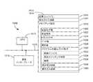
図15は、いくつかの実施形態による、メモリアレイを実装するためにコンポーネントのソフトウェア記述を含むコンピュータ可読ファイルを格納するためのシステム1500の一実施形態のブロック図である。システム1500は、1つまたは複数のデータ処理装置もしくは中央演算処理装置(CPU)1510と、メモリ1514と、(場合により)他のコンピュータシステムもしくはデバイスと情報を交換するための1つまたは複数の通信インターフェース1515と、これらのコンポーネントを互いに連結するための1つまたは複数の信号線もしくはコミュニケーションバス1512とを備えることができる。コミュニケーションバス1512は、システムコンポーネント間の通信を相互接続および制御する回路(チップセットと呼ばれる場合もある)を備えることができる。メモリ1514は、高速ランダムアクセスメモリ、例えば、DRAM、SRAM、DDR RAMまたは他のランダムアクセスソリッドステートメモリデバイスを含み、不揮発性メモリ、例えば、1つまたは複数の磁気ディスク記憶装置、光ディスク記憶装置、フラッシュメモリデバイスまたは他の不揮発性ソリッドステート記憶装置を含むことができる。メモリ1514は、場合により、CPU1510から離れて位置する1つまたは複数の記憶装置を含むことができる。メモリ1514またはその代わりのメモリ1514内の不揮発性メモリデバイスは、コンピュータ可読記憶媒体を備える。いくつかの実施形態では、メモリ1514は、上述の1つまたは複数のメモリデバイスに、回路コンパイラ1516、メモリアレイ記述1518および受光回路記述842を格納する。CPU1510などのプロセッサによって実行されると、回路コンパイラ1516は、1つまたは複数のメモリアレイ記述1518を処理し、1つまたは複数の対応する回路1517を統合する。 FIG. 15 is a block diagram of one embodiment of a
いくつかの実施形態では、メモリアレイ記述1518は、導電性平面1520、導電性列1522、トランジスタ1524、ビット線1526、選択線1528、プログラム可能なメモリ素子1530、読み取り回路1538および書き込み回路1540の記述を含む。いくつかの実施形態では、プログラム可能なメモリ素子1530の記述は、絶縁デバイス1532、抵抗スイッチング材料1534および電極1536の記述を含む。 In some embodiments, the
解釈する目的で、前述の説明は、特定の実施形態を参照して説明されている。しかし、上記の例示的考察は、網羅的であることまたは開示されたものと全く同一の形態に本発明を制限することを意図しない。上記の教示を考慮して、多くの変更形態および変形形態が可能である。実施形態は、本発明の原理および実用性を最も良く解釈するために選択および説明され、それにより、当業者は、企図される特定の用途に適したさまざまな変更形態を伴うさまざまな実施形態を実践することができる。 For the purpose of interpretation, the foregoing description has been described with reference to specific embodiments. However, the illustrative discussions above are not intended to be exhaustive or to limit the invention to the exact forms disclosed. Many modifications and variations are possible in light of the above teaching. The embodiments have been selected and described in order to best interpret the principles and utility of the present invention so that those skilled in the art will appreciate the various embodiments with various modifications suitable for the particular application contemplated. Can be practiced.
Claims (74)
Translated fromJapanese前記平面基板の上方の複数の水平な導電性平面と、
前記複数の水平な導電性平面と交互に配置される複数の水平な絶縁層と、
前記複数の導電性平面および絶縁層における開口部を通過する、前記複数の導電性平面および絶縁層と直角である垂直な導電性列のアレイと、
それぞれが前記水平な導電性平面の1つをそれぞれの垂直な導電性列に連結する、複数のプログラム可能なメモリ素子と
を備える、メモリデバイス。A planar substrate;
A plurality of horizontal conductive planes above the planar substrate;
A plurality of horizontal insulating layers arranged alternately with the plurality of horizontal conductive planes;
An array of vertical conductive columns passing through openings in the plurality of conductive planes and insulating layers and perpendicular to the plurality of conductive planes and insulating layers;
A memory device comprising a plurality of programmable memory elements, each connecting one of the horizontal conductive planes to a respective vertical conductive column.
前記垂直な導電性列がCuを含む、請求項2に記載のメモリデバイス。The resistive switching material comprises SiO2 ;
The memory device of claim 2, wherein the vertical conductive column comprises Cu.
前記垂直な導電性列がAgを含む、請求項2に記載のメモリデバイス。The resistive switching material comprises GeSe;
The memory device of claim 2, wherein the vertical conductive column comprises Ag.
前記垂直な導電性列がCuを含む、請求項2に記載のメモリデバイス。The resistive switching material comprises GeSe;
The memory device of claim 2, wherein the vertical conductive column comprises Cu.
前記垂直な導電性列がCuを含む、請求項2に記載のメモリデバイス。The resistive switching material comprises GeS;
The memory device of claim 2, wherein the vertical conductive column comprises Cu.
前記垂直な導電性列がCuを含む、請求項2に記載のメモリデバイス。The resistive switching material comprises CuO;
The memory device of claim 2, wherein the vertical conductive column comprises Cu.
前記金属層の積層体の前記不活性金属が、前記抵抗スイッチング材料に電気コンタクトを設ける、請求項25に記載のメモリデバイス。The programmable memory element comprises a resistive switching material having a first resistance state and a second resistance state;
26. The memory device of claim 25, wherein the inert metal of the metal layer stack provides electrical contact to the resistive switching material.
前記Ti−Pt−Ti積層体のPtが、前記抵抗スイッチング材料に電気コンタクトを設ける、請求項27に記載のメモリデバイス。The programmable memory element comprises a resistive switching material having a first resistance state and a second resistance state;
28. The memory device of claim 27, wherein Pt of the Ti-Pt-Ti stack provides an electrical contact to the resistive switching material.
水平な導電性平面を選択する工程と、
垂直な導電性列を選択する工程と、
前記選択された水平な導電性平面と前記選択された垂直な導電性列との間に電圧を印加し、前記選択された水平な導電性平面を前記選択された垂直な導電性列に連結するそれぞれのプログラム可能なメモリ素子をプログラミングする工程と
を含む、メモリデバイスをプログラミングする方法。A plurality of insulated horizontal conductive planes, an array of vertical conductive columns passing through openings in the plurality of horizontal conductive planes, and connecting the horizontal conductive planes to the vertical conductive columns A memory device comprising a plurality of programmable memory elements
Selecting a horizontal conductive plane;
Selecting a vertical conductive column;
A voltage is applied between the selected horizontal conductive plane and the selected vertical conductive column to couple the selected horizontal conductive plane to the selected vertical conductive column. Programming each of the programmable memory elements.
前記選択された水平な導電性平面と前記選択された垂直な導電性列との間に電圧を印加する工程が、前記選択された水平な導電性平面と前記信号線との間に電圧を印加する工程を含む、請求項35に記載の方法。Selecting the vertical conductive column comprises turning on a transistor to connect the vertical conductive column to a signal line;
Applying a voltage between the selected horizontal conductive plane and the selected vertical conductive column applies a voltage between the selected horizontal conductive plane and the signal line; 36. The method of claim 35, comprising the step of:
前記選択された水平な導電性平面と選択された垂直な導電性列との間に電圧を印加する工程が、前記関連するプログラミング電圧と前記閾値電圧との合計に対応するバイアスを印加する工程を含む、請求項35に記載の方法。The programmable memory element connecting the selected horizontal conductive plane to the selected vertical conductive column is a resistive switching material having an associated programming voltage, and a bi-directional conductivity when a threshold voltage is exceeded. An insulation device having
Applying a voltage between the selected horizontal conductive plane and a selected vertical conductive column comprises applying a bias corresponding to the sum of the associated programming voltage and the threshold voltage. 36. The method of claim 35, comprising.
水平な導電性平面を選択する工程と、
垂直な導電性列を選択する工程と、
前記選択された水平な導電性平面と、前記選択された垂直な導電性列に連結された信号線との間の抵抗に相当する電流または電圧を参照と比較し、前記選択された水平な導電性平面を前記選択された垂直な導電性列に連結するそれぞれのプログラム可能なメモリ素子の状態を判断する工程と
を含む、メモリデバイスを読み取る方法。A plurality of insulated horizontal conductive planes, an array of vertical conductive columns passing through openings in the plurality of horizontal conductive planes, and coupling the vertical conductive columns to the horizontal conductive planes A memory device comprising a plurality of programmable memory elements
Selecting a horizontal conductive plane;
Selecting a vertical conductive column;
A current or voltage corresponding to a resistance between the selected horizontal conductive plane and a signal line coupled to the selected vertical conductive column is compared with a reference, and the selected horizontal conductive Determining a state of each programmable memory element coupling a sex plane to the selected vertical conductive column.
前記比較する工程が、前記読み取り電圧と前記閾値電圧との合計に対応する電圧を、前記選択された水平な導電性平面と、前記選択された垂直な導電性列に連結する信号線との間に印加する工程を含む、請求項38に記載の方法。Each programmable memory element comprises a resistive switching material having an associated read voltage and an isolation device having bidirectional conductivity above a threshold voltage;
The comparing step includes a voltage corresponding to a sum of the read voltage and the threshold voltage between the selected horizontal conductive plane and a signal line connecting the selected vertical conductive column. 40. The method of claim 38, comprising the step of applying to:
前記抵抗スイッチング材料と直列に配置され、閾値電圧を超えると双方向導電性を有する絶縁デバイスと
を備える、メモリセル。A resistance switching material having a first resistance state and a second resistance state, wherein the second resistance state has a lower resistance than the first resistance state;
A memory cell comprising an insulating device disposed in series with the resistive switching material and having bidirectional conductivity when a threshold voltage is exceeded.
前記絶縁デバイスが、前記開口部の第3の部分に位置する絶縁材料を備える、請求項41に記載のメモリセル。The resistive switching material is located in a first portion of an opening in a horizontal conductive plane and is connected to a vertical bit line in a second portion of the opening;
42. The memory cell of claim 41, wherein the insulating device comprises an insulating material located in a third portion of the opening.
前記絶縁デバイスが、前記抵抗スイッチング材料の平面リングと同心円状の絶縁材料の平面リングを備える、請求項41に記載のメモリセル。The resistive switching material comprises a planar ring of the resistive switching material, the planar ring surrounding a vertical bit line;
42. The memory cell of claim 41, wherein the isolation device comprises a planar ring of insulating material concentric with the planar ring of resistive switching material.
前記絶縁材料の平面リングがAl2O3を含む、請求項51に記載のメモリセル。The horizontal conductive plane comprises Al;
Planar ring of said insulating material comprisesAl 2O 3, the memory cell of claim 51.
前記複数の交互に位置する導電性平面および絶縁平面を貫通する形で複数のビアにエッチングを施す工程と、
抵抗スイッチング材料を前記複数のビアの側壁に共形に堆積させる工程と、
第1の金属を前記ビアに堆積させ、前記抵抗スイッチング材料に電気コンタクトを設ける工程であって、前記堆積させた第1の金属が導電性列を形成する、工程と
を含む、三次元メモリアレイを製作する方法。Producing a plurality of alternating insulating and conductive planes above the planar substrate;
Etching a plurality of vias through the plurality of alternating conductive and insulating planes; and
Conformally depositing resistive switching material on sidewalls of the plurality of vias;
Depositing a first metal in the via and providing an electrical contact to the resistive switching material, wherein the deposited first metal forms a conductive column. How to make.
複数のトランジスタを製作してそれぞれの信号線をそれぞれの導電性列に連結する工程とをさらに含む、請求項56に記載の方法。Producing a plurality of parallel signal lines on the planar substrate;
57. The method of claim 56, further comprising fabricating a plurality of transistors to connect each signal line to a respective conductive column.
前記ビアにポリシリコンを堆積させる工程と、
ガルバニック置換を使用して前記ポリシリコンを前記第1の金属と置き換える工程とを含む、請求項56に記載の方法。Depositing the first metal on the vias;
Depositing polysilicon in the via;
57. The method of claim 56, comprising using galvanic substitution to replace the polysilicon with the first metal.
前記抵抗スイッチング材料を前記第2の金属に堆積させる、請求項65に記載の方法。Depositing a second metal on the polysilicon exposed on the via sidewalls using galvanic substitution after etching the plurality of vias and before conformally depositing the resistive switching material; Including
66. The method of claim 65, wherein the resistive switching material is deposited on the second metal.
前記第1の金属を前記ビアに堆積させる工程が、Cu膜を前記SiO2に共形に堆積させる工程を含む、請求項66に記載の方法。The resistive switching material comprises SiO2 ;
Depositing said first metal on the via comprises depositing conformally a Cu film on the SiO2, The method of claim 66.
ポリシリコンを前記ビアに共形に堆積させる工程と、
ガルバニック置換を使用して、堆積させたポリシリコンをCuと置き換える工程とを含む、請求項68に記載の方法。Depositing the Cu film conformally on the SiO2 ;
Depositing polysilicon conformally on the via;
69. The method of claim 68, comprising using galvanic replacement to replace the deposited polysilicon with Cu.
前記抵抗スイッチング材料を共形に堆積させる前に、
前記凹部に絶縁体を形成する工程と、
第2の金属を前記凹部の絶縁体に堆積させる工程とをさらに含み、
前記抵抗スイッチング材料を前記第2の金属に堆積させる、請求項56に記載の方法。Etching the plurality of vias includes undercutting the conductive plane as it is exposed along the sidewalls of the vias to form recesses along the sidewalls;
Prior to conformally depositing the resistive switching material,
Forming an insulator in the recess;
Depositing a second metal on the insulator in the recess,
57. The method of claim 56, wherein the resistive switching material is deposited on the second metal.
前記絶縁体を形成する工程が、前記凹部で露出しているAlに陽極酸化処理を施してAl2O3を形成する工程を含む、請求項70に記載の方法。The conductive plane includes Al;
It said step of forming the insulator, comprising the step of forming the Al2 O3 is subjected to anodization Al exposed in the recess 71. The method of claim 70.
前記第2の金属を前記側壁に沿って堆積させる工程と、
前記堆積させた第2の金属にエッチングを施して、前記凹部以外の第2の金属を除去する工程とを含む、請求項70に記載の方法。Depositing the second metal on the insulator in the recess,
Depositing the second metal along the sidewall;
71. The method of claim 70, further comprising: etching the deposited second metal to remove the second metal other than the recess.
ポリシリコンを前記側壁に沿って堆積させる工程と、
ガルバニック置換を使用して前記ポリシリコンを前記第2の金属と置き換える工程とを含む、請求項70に記載の方法。Depositing the second metal on the insulator in the recess forming the insulator;
Depositing polysilicon along the sidewall;
71. The method of claim 70, comprising using galvanic substitution to replace the polysilicon with the second metal.
Applications Claiming Priority (3)
| Application Number | Priority Date | Filing Date | Title |
|---|---|---|---|
| US25907009P | 2009-11-06 | 2009-11-06 | |
| US61/259,070 | 2009-11-06 | ||
| PCT/US2010/046831WO2011056281A1 (en) | 2009-11-06 | 2010-08-26 | Three-dimensional memory array stacking structure |
Publications (1)
| Publication Number | Publication Date |
|---|---|
| JP2013510438Atrue JP2013510438A (en) | 2013-03-21 |
Family
ID=43970224
Family Applications (1)
| Application Number | Title | Priority Date | Filing Date |
|---|---|---|---|
| JP2012537877APendingJP2013510438A (en) | 2009-11-06 | 2010-08-26 | Three-dimensional memory array stack structure |
Country Status (4)
| Country | Link |
|---|---|
| US (1) | US8716780B2 (en) |
| JP (1) | JP2013510438A (en) |
| KR (1) | KR20120104992A (en) |
| WO (1) | WO2011056281A1 (en) |
Cited By (5)
| Publication number | Priority date | Publication date | Assignee | Title |
|---|---|---|---|---|
| US9236124B2 (en) | 2014-03-07 | 2016-01-12 | Kabushiki Kaisha Toshiba | Nonvolatile memory device |
| WO2016060973A1 (en)* | 2014-10-16 | 2016-04-21 | Micron Technology, Inc. | Select device for memory cell applications |
| JP2016527710A (en)* | 2013-06-11 | 2016-09-08 | マイクロン テクノロジー, インク. | Three-dimensional memory array with a selection device |
| JP2016534572A (en)* | 2013-09-09 | 2016-11-04 | クアルコム,インコーポレイテッド | Vertical tunnel field effect transistor |
| JP2024515438A (en)* | 2021-03-30 | 2024-04-10 | インターナショナル・ビジネス・マシーンズ・コーポレーション | Non-volatile tunable capacitive processing unit |
Families Citing this family (123)
| Publication number | Priority date | Publication date | Assignee | Title |
|---|---|---|---|---|
| US9030859B2 (en) | 2010-12-14 | 2015-05-12 | Sandisk 3D Llc | Three dimensional non-volatile storage with dual layers of select devices |
| US9227456B2 (en)* | 2010-12-14 | 2016-01-05 | Sandisk 3D Llc | Memories with cylindrical read/write stacks |
| US10283321B2 (en) | 2011-01-18 | 2019-05-07 | Applied Materials, Inc. | Semiconductor processing system and methods using capacitively coupled plasma |
| JP5676364B2 (en)* | 2011-05-27 | 2015-02-25 | 株式会社日立製作所 | Semiconductor memory device |
| KR20130071006A (en)* | 2011-12-20 | 2013-06-28 | 삼성전자주식회사 | Variable resistance memory device and method of forming the same |
| US9093369B2 (en)* | 2012-06-07 | 2015-07-28 | Samsung Electronics Co., Ltd. | Three-dimensional resistive random access memory devices, methods of operating the same, and methods of fabricating the same |
| KR102010928B1 (en)* | 2012-06-07 | 2019-10-21 | 삼성전자주식회사 | Resistive random-access memory device, methods of operating and fabricating the same |
| TWI497707B (en)* | 2012-08-01 | 2015-08-21 | Macronix Int Co Ltd | Three-dimensional array structure for memory devices |
| US9373517B2 (en) | 2012-08-02 | 2016-06-21 | Applied Materials, Inc. | Semiconductor processing with DC assisted RF power for improved control |
| JP5996324B2 (en)* | 2012-08-07 | 2016-09-21 | シャープ株式会社 | Nonvolatile semiconductor memory device and manufacturing method thereof |
| US9117503B2 (en) | 2012-08-29 | 2015-08-25 | Micron Technology, Inc. | Memory array plane select and methods |
| US9132436B2 (en) | 2012-09-21 | 2015-09-15 | Applied Materials, Inc. | Chemical control features in wafer process equipment |
| US10256079B2 (en) | 2013-02-08 | 2019-04-09 | Applied Materials, Inc. | Semiconductor processing systems having multiple plasma configurations |
| US9362130B2 (en) | 2013-03-01 | 2016-06-07 | Applied Materials, Inc. | Enhanced etching processes using remote plasma sources |
| US9165933B2 (en) | 2013-03-07 | 2015-10-20 | Sandisk 3D Llc | Vertical bit line TFT decoder for high voltage operation |
| US9123640B2 (en)* | 2013-05-13 | 2015-09-01 | Seagate Technology Llc | Three dimensional resistive memory |
| US8953387B2 (en) | 2013-06-10 | 2015-02-10 | Micron Technology, Inc. | Apparatuses and methods for efficient write in a cross-point array |
| US9337210B2 (en) | 2013-08-12 | 2016-05-10 | Micron Technology, Inc. | Vertical ferroelectric field effect transistor constructions, constructions comprising a pair of vertical ferroelectric field effect transistors, vertical strings of ferroelectric field effect transistors, and vertical strings of laterally opposing pairs of vertical ferroelectric field effect transistors |
| TWI506649B (en)* | 2013-08-30 | 2015-11-01 | Micron Technology Inc | Memory array plane select |
| US9312005B2 (en) | 2013-09-10 | 2016-04-12 | Micron Technology, Inc. | Accessing memory cells in parallel in a cross-point array |
| US9343322B2 (en)* | 2014-01-17 | 2016-05-17 | Macronix International Co., Ltd. | Three dimensional stacking memory film structure |
| US9425237B2 (en) | 2014-03-11 | 2016-08-23 | Crossbar, Inc. | Selector device for two-terminal memory |
| US9263577B2 (en) | 2014-04-24 | 2016-02-16 | Micron Technology, Inc. | Ferroelectric field effect transistors, pluralities of ferroelectric field effect transistors arrayed in row lines and column lines, and methods of forming a plurality of ferroelectric field effect transistors |
| US9324423B2 (en) | 2014-05-07 | 2016-04-26 | Micron Technology, Inc. | Apparatuses and methods for bi-directional access of cross-point arrays |
| US9309598B2 (en) | 2014-05-28 | 2016-04-12 | Applied Materials, Inc. | Oxide and metal removal |
| US10211397B1 (en) | 2014-07-07 | 2019-02-19 | Crossbar, Inc. | Threshold voltage tuning for a volatile selection device |
| US9633724B2 (en) | 2014-07-07 | 2017-04-25 | Crossbar, Inc. | Sensing a non-volatile memory device utilizing selector device holding characteristics |
| US9460788B2 (en) | 2014-07-09 | 2016-10-04 | Crossbar, Inc. | Non-volatile memory cell utilizing volatile switching two terminal device and a MOS transistor |
| US10115819B2 (en) | 2015-05-29 | 2018-10-30 | Crossbar, Inc. | Recessed high voltage metal oxide semiconductor transistor for RRAM cell |
| US9437658B2 (en)* | 2014-08-05 | 2016-09-06 | Sandisk Technologies Llc | Fully isolated selector for memory device |
| US9159829B1 (en) | 2014-10-07 | 2015-10-13 | Micron Technology, Inc. | Recessed transistors containing ferroelectric material |
| US9355922B2 (en) | 2014-10-14 | 2016-05-31 | Applied Materials, Inc. | Systems and methods for internal surface conditioning in plasma processing equipment |
| US9966240B2 (en) | 2014-10-14 | 2018-05-08 | Applied Materials, Inc. | Systems and methods for internal surface conditioning assessment in plasma processing equipment |
| US11637002B2 (en) | 2014-11-26 | 2023-04-25 | Applied Materials, Inc. | Methods and systems to enhance process uniformity |
| US10224210B2 (en) | 2014-12-09 | 2019-03-05 | Applied Materials, Inc. | Plasma processing system with direct outlet toroidal plasma source |
| US10573496B2 (en) | 2014-12-09 | 2020-02-25 | Applied Materials, Inc. | Direct outlet toroidal plasma source |
| US11257693B2 (en) | 2015-01-09 | 2022-02-22 | Applied Materials, Inc. | Methods and systems to improve pedestal temperature control |
| US20160225652A1 (en) | 2015-02-03 | 2016-08-04 | Applied Materials, Inc. | Low temperature chuck for plasma processing systems |
| US9728437B2 (en) | 2015-02-03 | 2017-08-08 | Applied Materials, Inc. | High temperature chuck for plasma processing systems |
| US9305929B1 (en) | 2015-02-17 | 2016-04-05 | Micron Technology, Inc. | Memory cells |
| US9595669B2 (en) | 2015-06-30 | 2017-03-14 | Western Digital Technologies, Inc. | Electroplated phase change switch |
| US10134982B2 (en)* | 2015-07-24 | 2018-11-20 | Micron Technology, Inc. | Array of cross point memory cells |
| US9853211B2 (en) | 2015-07-24 | 2017-12-26 | Micron Technology, Inc. | Array of cross point memory cells individually comprising a select device and a programmable device |
| US9691645B2 (en) | 2015-08-06 | 2017-06-27 | Applied Materials, Inc. | Bolted wafer chuck thermal management systems and methods for wafer processing systems |
| US9741593B2 (en) | 2015-08-06 | 2017-08-22 | Applied Materials, Inc. | Thermal management systems and methods for wafer processing systems |
| US9349605B1 (en) | 2015-08-07 | 2016-05-24 | Applied Materials, Inc. | Oxide etch selectivity systems and methods |
| TWI575714B (en)* | 2015-08-14 | 2017-03-21 | 旺宏電子股份有限公司 | Three-dimensional memory |
| US10504700B2 (en) | 2015-08-27 | 2019-12-10 | Applied Materials, Inc. | Plasma etching systems and methods with secondary plasma injection |
| US9564585B1 (en) | 2015-09-03 | 2017-02-07 | HGST Netherlands B.V. | Multi-level phase change device |
| US9812505B2 (en) | 2015-11-16 | 2017-11-07 | Sandisk Technologies Llc | Non-volatile memory device containing oxygen-scavenging material portions and method of making thereof |
| US9947721B2 (en) | 2016-04-01 | 2018-04-17 | Micron Technology, Inc. | Thermal insulation for three-dimensional memory arrays |
| US10522371B2 (en) | 2016-05-19 | 2019-12-31 | Applied Materials, Inc. | Systems and methods for improved semiconductor etching and component protection |
| US10504754B2 (en) | 2016-05-19 | 2019-12-10 | Applied Materials, Inc. | Systems and methods for improved semiconductor etching and component protection |
| US9865484B1 (en) | 2016-06-29 | 2018-01-09 | Applied Materials, Inc. | Selective etch using material modification and RF pulsing |
| US10062575B2 (en) | 2016-09-09 | 2018-08-28 | Applied Materials, Inc. | Poly directional etch by oxidation |
| US10629473B2 (en) | 2016-09-09 | 2020-04-21 | Applied Materials, Inc. | Footing removal for nitride spacer |
| US10062585B2 (en) | 2016-10-04 | 2018-08-28 | Applied Materials, Inc. | Oxygen compatible plasma source |
| US9934942B1 (en) | 2016-10-04 | 2018-04-03 | Applied Materials, Inc. | Chamber with flow-through source |
| US10546729B2 (en) | 2016-10-04 | 2020-01-28 | Applied Materials, Inc. | Dual-channel showerhead with improved profile |
| US10062579B2 (en) | 2016-10-07 | 2018-08-28 | Applied Materials, Inc. | Selective SiN lateral recess |
| US9947549B1 (en) | 2016-10-10 | 2018-04-17 | Applied Materials, Inc. | Cobalt-containing material removal |
| US9768034B1 (en) | 2016-11-11 | 2017-09-19 | Applied Materials, Inc. | Removal methods for high aspect ratio structures |
| US10163696B2 (en) | 2016-11-11 | 2018-12-25 | Applied Materials, Inc. | Selective cobalt removal for bottom up gapfill |
| US10242908B2 (en) | 2016-11-14 | 2019-03-26 | Applied Materials, Inc. | Airgap formation with damage-free copper |
| US10026621B2 (en) | 2016-11-14 | 2018-07-17 | Applied Materials, Inc. | SiN spacer profile patterning |
| KR102673120B1 (en)* | 2016-12-05 | 2024-06-05 | 삼성전자주식회사 | Semiconductor device and method for fabricating the same |
| US10566206B2 (en)* | 2016-12-27 | 2020-02-18 | Applied Materials, Inc. | Systems and methods for anisotropic material breakthrough |
| US10396145B2 (en) | 2017-01-12 | 2019-08-27 | Micron Technology, Inc. | Memory cells comprising ferroelectric material and including current leakage paths having different total resistances |
| US10431429B2 (en) | 2017-02-03 | 2019-10-01 | Applied Materials, Inc. | Systems and methods for radial and azimuthal control of plasma uniformity |
| US10403507B2 (en) | 2017-02-03 | 2019-09-03 | Applied Materials, Inc. | Shaped etch profile with oxidation |
| US10043684B1 (en) | 2017-02-06 | 2018-08-07 | Applied Materials, Inc. | Self-limiting atomic thermal etching systems and methods |
| US10319739B2 (en) | 2017-02-08 | 2019-06-11 | Applied Materials, Inc. | Accommodating imperfectly aligned memory holes |
| US10943834B2 (en) | 2017-03-13 | 2021-03-09 | Applied Materials, Inc. | Replacement contact process |
| US10096362B1 (en) | 2017-03-24 | 2018-10-09 | Crossbar, Inc. | Switching block configuration bit comprising a non-volatile memory cell |
| US10319649B2 (en) | 2017-04-11 | 2019-06-11 | Applied Materials, Inc. | Optical emission spectroscopy (OES) for remote plasma monitoring |
| US11276590B2 (en) | 2017-05-17 | 2022-03-15 | Applied Materials, Inc. | Multi-zone semiconductor substrate supports |
| JP7176860B6 (en) | 2017-05-17 | 2022-12-16 | アプライド マテリアルズ インコーポレイテッド | Semiconductor processing chamber to improve precursor flow |
| US11276559B2 (en) | 2017-05-17 | 2022-03-15 | Applied Materials, Inc. | Semiconductor processing chamber for multiple precursor flow |
| US10049891B1 (en) | 2017-05-31 | 2018-08-14 | Applied Materials, Inc. | Selective in situ cobalt residue removal |
| US10497579B2 (en) | 2017-05-31 | 2019-12-03 | Applied Materials, Inc. | Water-free etching methods |
| US10920320B2 (en) | 2017-06-16 | 2021-02-16 | Applied Materials, Inc. | Plasma health determination in semiconductor substrate processing reactors |
| US10115899B1 (en) | 2017-06-23 | 2018-10-30 | Sandisk Technologies Llc | Methods and apparatus for three-dimensional nonvolatile memory |
| US10541246B2 (en) | 2017-06-26 | 2020-01-21 | Applied Materials, Inc. | 3D flash memory cells which discourage cross-cell electrical tunneling |
| US10727080B2 (en) | 2017-07-07 | 2020-07-28 | Applied Materials, Inc. | Tantalum-containing material removal |
| US10541184B2 (en) | 2017-07-11 | 2020-01-21 | Applied Materials, Inc. | Optical emission spectroscopic techniques for monitoring etching |
| US10354889B2 (en) | 2017-07-17 | 2019-07-16 | Applied Materials, Inc. | Non-halogen etching of silicon-containing materials |
| US10170336B1 (en) | 2017-08-04 | 2019-01-01 | Applied Materials, Inc. | Methods for anisotropic control of selective silicon removal |
| US10043674B1 (en) | 2017-08-04 | 2018-08-07 | Applied Materials, Inc. | Germanium etching systems and methods |
| US10297458B2 (en) | 2017-08-07 | 2019-05-21 | Applied Materials, Inc. | Process window widening using coated parts in plasma etch processes |
| US10283324B1 (en) | 2017-10-24 | 2019-05-07 | Applied Materials, Inc. | Oxygen treatment for nitride etching |
| US10128086B1 (en) | 2017-10-24 | 2018-11-13 | Applied Materials, Inc. | Silicon pretreatment for nitride removal |
| US10256112B1 (en) | 2017-12-08 | 2019-04-09 | Applied Materials, Inc. | Selective tungsten removal |
| US10903054B2 (en) | 2017-12-19 | 2021-01-26 | Applied Materials, Inc. | Multi-zone gas distribution systems and methods |
| US11328909B2 (en) | 2017-12-22 | 2022-05-10 | Applied Materials, Inc. | Chamber conditioning and removal processes |
| US10854426B2 (en) | 2018-01-08 | 2020-12-01 | Applied Materials, Inc. | Metal recess for semiconductor structures |
| US10964512B2 (en) | 2018-02-15 | 2021-03-30 | Applied Materials, Inc. | Semiconductor processing chamber multistage mixing apparatus and methods |
| US10679870B2 (en) | 2018-02-15 | 2020-06-09 | Applied Materials, Inc. | Semiconductor processing chamber multistage mixing apparatus |
| TWI766433B (en) | 2018-02-28 | 2022-06-01 | 美商應用材料股份有限公司 | Systems and methods to form airgaps |
| US10593560B2 (en) | 2018-03-01 | 2020-03-17 | Applied Materials, Inc. | Magnetic induction plasma source for semiconductor processes and equipment |
| US10319600B1 (en) | 2018-03-12 | 2019-06-11 | Applied Materials, Inc. | Thermal silicon etch |
| US10497573B2 (en) | 2018-03-13 | 2019-12-03 | Applied Materials, Inc. | Selective atomic layer etching of semiconductor materials |
| US10573527B2 (en) | 2018-04-06 | 2020-02-25 | Applied Materials, Inc. | Gas-phase selective etching systems and methods |
| US10490406B2 (en) | 2018-04-10 | 2019-11-26 | Appled Materials, Inc. | Systems and methods for material breakthrough |
| US10699879B2 (en) | 2018-04-17 | 2020-06-30 | Applied Materials, Inc. | Two piece electrode assembly with gap for plasma control |
| US10886137B2 (en) | 2018-04-30 | 2021-01-05 | Applied Materials, Inc. | Selective nitride removal |
| WO2019236162A1 (en)* | 2018-06-07 | 2019-12-12 | Sandisk Technologies Llc | Three-dimensional phase change memory array including discrete middle electrodes and methods of making the same |
| US10381409B1 (en) | 2018-06-07 | 2019-08-13 | Sandisk Technologies Llc | Three-dimensional phase change memory array including discrete middle electrodes and methods of making the same |
| US10381559B1 (en) | 2018-06-07 | 2019-08-13 | Sandisk Technologies Llc | Three-dimensional phase change memory array including discrete middle electrodes and methods of making the same |
| US10755941B2 (en) | 2018-07-06 | 2020-08-25 | Applied Materials, Inc. | Self-limiting selective etching systems and methods |
| US10872778B2 (en) | 2018-07-06 | 2020-12-22 | Applied Materials, Inc. | Systems and methods utilizing solid-phase etchants |
| US10672642B2 (en) | 2018-07-24 | 2020-06-02 | Applied Materials, Inc. | Systems and methods for pedestal configuration |
| US10892198B2 (en) | 2018-09-14 | 2021-01-12 | Applied Materials, Inc. | Systems and methods for improved performance in semiconductor processing |
| US11049755B2 (en) | 2018-09-14 | 2021-06-29 | Applied Materials, Inc. | Semiconductor substrate supports with embedded RF shield |
| US11062887B2 (en) | 2018-09-17 | 2021-07-13 | Applied Materials, Inc. | High temperature RF heater pedestals |
| US11417534B2 (en) | 2018-09-21 | 2022-08-16 | Applied Materials, Inc. | Selective material removal |
| US11682560B2 (en) | 2018-10-11 | 2023-06-20 | Applied Materials, Inc. | Systems and methods for hafnium-containing film removal |
| US11121002B2 (en) | 2018-10-24 | 2021-09-14 | Applied Materials, Inc. | Systems and methods for etching metals and metal derivatives |
| US11437242B2 (en) | 2018-11-27 | 2022-09-06 | Applied Materials, Inc. | Selective removal of silicon-containing materials |
| US11721527B2 (en) | 2019-01-07 | 2023-08-08 | Applied Materials, Inc. | Processing chamber mixing systems |
| US10920319B2 (en) | 2019-01-11 | 2021-02-16 | Applied Materials, Inc. | Ceramic showerheads with conductive electrodes |
| US10839900B1 (en)* | 2019-06-12 | 2020-11-17 | International Business Machines Corporation | Parasitic voltage drop compensation in large cross-point arrays |
| US11170834B2 (en) | 2019-07-10 | 2021-11-09 | Micron Technology, Inc. | Memory cells and methods of forming a capacitor including current leakage paths having different total resistances |
| KR102845400B1 (en) | 2020-09-25 | 2025-08-13 | 삼성전자주식회사 | Variable resistance memory device |
Citations (5)
| Publication number | Priority date | Publication date | Assignee | Title |
|---|---|---|---|---|
| JP2007194637A (en)* | 2006-01-19 | 2007-08-02 | Samsung Electronics Co Ltd | Resistive memory device having varistor and method of operating the same |
| JP2008181978A (en)* | 2007-01-23 | 2008-08-07 | Toshiba Corp | Semiconductor memory device and manufacturing method thereof |
| JP2008244018A (en)* | 2007-03-26 | 2008-10-09 | Ulvac Japan Ltd | Manufacturing method of semiconductor device |
| JP2009004725A (en)* | 2007-09-25 | 2009-01-08 | Panasonic Corp | Variable resistance nonvolatile memory device |
| JP2009081251A (en)* | 2007-09-26 | 2009-04-16 | Panasonic Corp | Resistance change element, manufacturing method thereof, and resistance change type memory |
Family Cites Families (22)
| Publication number | Priority date | Publication date | Assignee | Title |
|---|---|---|---|---|
| US6034882A (en) | 1998-11-16 | 2000-03-07 | Matrix Semiconductor, Inc. | Vertically stacked field programmable nonvolatile memory and method of fabrication |
| EP1271652A3 (en)* | 2001-06-22 | 2004-05-06 | Fujio Masuoka | A semiconductor memory and its production process |
| US7009278B2 (en) | 2003-11-24 | 2006-03-07 | Sharp Laboratories Of America, Inc. | 3d rram |
| US7112815B2 (en)* | 2004-02-25 | 2006-09-26 | Micron Technology, Inc. | Multi-layer memory arrays |
| US20070132049A1 (en) | 2005-12-12 | 2007-06-14 | Stipe Barry C | Unipolar resistance random access memory (RRAM) device and vertically stacked architecture |
| FR2910686B1 (en)* | 2006-12-20 | 2009-04-03 | Commissariat Energie Atomique | MEMORIZATION DEVICE WITH MULTI-LEVEL STRUCTURE |
| KR100881292B1 (en) | 2007-01-23 | 2009-02-04 | 삼성전자주식회사 | Resistive semiconductor memory device having a three-dimensional stacked structure and control method thereof |
| FR2913523B1 (en)* | 2007-03-09 | 2009-06-05 | Commissariat Energie Atomique | MULTI-LEVEL DATA STORAGE DEVICE WITH PHASE CHANGE MATERIAL |
| JP2009117006A (en) | 2007-11-09 | 2009-05-28 | Toshiba Corp | Resistance change memory device |
| JP4649487B2 (en)* | 2008-03-17 | 2011-03-09 | 株式会社東芝 | Nonvolatile semiconductor memory device and manufacturing method thereof |
| KR101424176B1 (en)* | 2008-03-21 | 2014-07-31 | 삼성전자주식회사 | Nonvolatile memory device using variable resistive element, memory system comprising the same |
| KR101539697B1 (en)* | 2008-06-11 | 2015-07-27 | 삼성전자주식회사 | A three-dimensional memory device using a vertical pillar as an active region, a method of manufacturing the same, and a method of operating the same |
| KR20100007229A (en)* | 2008-07-11 | 2010-01-22 | 삼성전자주식회사 | Non-volatile memory device and method of fabricating the same |
| KR20080091416A (en)* | 2008-08-14 | 2008-10-13 | 김성동 | 3D semiconductor device, manufacturing method and operating method thereof |
| JP2010080685A (en)* | 2008-09-26 | 2010-04-08 | Toshiba Corp | Nonvolatile storage device and method for fabricating the same |
| KR101498676B1 (en)* | 2008-09-30 | 2015-03-09 | 삼성전자주식회사 | Three-dimensional semiconductor device |
| KR100979906B1 (en)* | 2008-10-09 | 2010-09-06 | 서울대학교산학협력단 | Highly Integrated Flash Memory Cell Stacks, Cell Stack Strings, and Manufacturing Methods Thereof |
| JP5489449B2 (en)* | 2008-12-10 | 2014-05-14 | 株式会社東芝 | Nonvolatile semiconductor memory device and manufacturing method thereof |
| JP5317664B2 (en)* | 2008-12-17 | 2013-10-16 | 株式会社東芝 | Method for manufacturing nonvolatile semiconductor memory device |
| US8546861B2 (en)* | 2009-03-05 | 2013-10-01 | Gwangju Institute Of Science And Technology | Resistance change memory device with three-dimensional structure, and device array, electronic product and manufacturing method therefor |
| US8173987B2 (en)* | 2009-04-27 | 2012-05-08 | Macronix International Co., Ltd. | Integrated circuit 3D phase change memory array and manufacturing method |
| US8461566B2 (en)* | 2009-11-02 | 2013-06-11 | Micron Technology, Inc. | Methods, structures and devices for increasing memory density |
- 2010
- 2010-08-26JPJP2012537877Apatent/JP2013510438A/enactivePending
- 2010-08-26WOPCT/US2010/046831patent/WO2011056281A1/enactiveApplication Filing
- 2010-08-26USUS13/505,442patent/US8716780B2/enactiveActive
- 2010-08-26KRKR1020127014634Apatent/KR20120104992A/ennot_activeCeased
Patent Citations (5)
| Publication number | Priority date | Publication date | Assignee | Title |
|---|---|---|---|---|
| JP2007194637A (en)* | 2006-01-19 | 2007-08-02 | Samsung Electronics Co Ltd | Resistive memory device having varistor and method of operating the same |
| JP2008181978A (en)* | 2007-01-23 | 2008-08-07 | Toshiba Corp | Semiconductor memory device and manufacturing method thereof |
| JP2008244018A (en)* | 2007-03-26 | 2008-10-09 | Ulvac Japan Ltd | Manufacturing method of semiconductor device |
| JP2009004725A (en)* | 2007-09-25 | 2009-01-08 | Panasonic Corp | Variable resistance nonvolatile memory device |
| JP2009081251A (en)* | 2007-09-26 | 2009-04-16 | Panasonic Corp | Resistance change element, manufacturing method thereof, and resistance change type memory |
Cited By (12)
| Publication number | Priority date | Publication date | Assignee | Title |
|---|---|---|---|---|
| JP2016527710A (en)* | 2013-06-11 | 2016-09-08 | マイクロン テクノロジー, インク. | Three-dimensional memory array with a selection device |
| US9728584B2 (en) | 2013-06-11 | 2017-08-08 | Micron Technology, Inc. | Three dimensional memory array with select device |
| US10134810B2 (en) | 2013-06-11 | 2018-11-20 | Micron Technology, Inc. | Three dimensional memory array with select device |
| US10916586B2 (en) | 2013-06-11 | 2021-02-09 | Micron Technology, Inc. | Three dimensional memory array with select device |
| JP2016534572A (en)* | 2013-09-09 | 2016-11-04 | クアルコム,インコーポレイテッド | Vertical tunnel field effect transistor |
| US9236124B2 (en) | 2014-03-07 | 2016-01-12 | Kabushiki Kaisha Toshiba | Nonvolatile memory device |
| WO2016060973A1 (en)* | 2014-10-16 | 2016-04-21 | Micron Technology, Inc. | Select device for memory cell applications |
| US9425390B2 (en) | 2014-10-16 | 2016-08-23 | Micron Technology, Inc. | Select device for memory cell applications |
| US9735200B2 (en) | 2014-10-16 | 2017-08-15 | Micron Technology, Inc. | Select device for memory cell applications |
| US10109677B2 (en) | 2014-10-16 | 2018-10-23 | Micron Technology, Inc. | Select device for memory cell applications |
| US10608048B2 (en) | 2014-10-16 | 2020-03-31 | Micron Technology, Inc. | Select device for memory cell applications |
| JP2024515438A (en)* | 2021-03-30 | 2024-04-10 | インターナショナル・ビジネス・マシーンズ・コーポレーション | Non-volatile tunable capacitive processing unit |
Also Published As
| Publication number | Publication date |
|---|---|
| WO2011056281A1 (en) | 2011-05-12 |
| US8716780B2 (en) | 2014-05-06 |
| KR20120104992A (en) | 2012-09-24 |
| US20120211722A1 (en) | 2012-08-23 |
Similar Documents
| Publication | Publication Date | Title |
|---|---|---|
| JP2013510438A (en) | Three-dimensional memory array stack structure | |
| US12380930B2 (en) | Memory array decoding and interconnects | |
| US11903223B2 (en) | Thin film transistors and related fabrication techniques | |
| KR101893643B1 (en) | Rram device with data storage layer having increased height | |
| TWI462357B (en) | Vertical memory cell for high-density memory | |
| US9286979B2 (en) | Method and structure for resistive switching random access memory with high reliable and high density | |
| US7791057B2 (en) | Memory cell having a buried phase change region and method for fabricating the same | |
| TWI540775B (en) | Resistance change nonvolatile memory device, semiconductor device, and method of operating resistance change nonvolatile memory device | |
| TWI400796B (en) | Phase change memory with dual word lines and source lines and method of operating same | |
| CN104813471B (en) | Vertical cross-point embedded memory architecture for metal-conducting oxide-metal (MCOM) memory elements | |
| US20200303639A1 (en) | Memory device and method of forming the same | |
| US20140034896A1 (en) | Nonvolatile Memory Cells And Methods Of Forming Nonvolatile Memory Cells | |
| US9099385B2 (en) | Vertical 1T-1R memory cells, memory arrays and methods of forming the same | |
| JP2006040946A (en) | Memory element | |
| US20150162383A1 (en) | Vertical resistive random access memory device, and method for manufacturing same | |
| CN105940516A (en) | Resistive memory cell having a reduced conductive path area | |
| US8218359B2 (en) | Phase change random access memory and methods of manufacturing and operating same | |
| US20160351261A1 (en) | Content addressable memory cells, memory arrays and methods of forming the same | |
| KR101511421B1 (en) | 3-Dimensional Memory of using Multi-layered Phase Change Material | |
| WO2017052583A1 (en) | Thermally insulated resistive random access memory | |
| TWI868329B (en) | Semiconductor memory device and fabrication method thereof | |
| JP2011049581A (en) | Storage element and operating method of storage element | |
| KR20220159394A (en) | Dual damascene crossbar array for disabling defective resistive switching devices in the array | |
| TW202443858A (en) | Memory device and method for manufacturing the same | |
| JP2006324425A (en) | Manufacturing method of memory element |
Legal Events
| Date | Code | Title | Description |
|---|---|---|---|
| A977 | Report on retrieval | Free format text:JAPANESE INTERMEDIATE CODE: A971007 Effective date:20131115 | |
| A131 | Notification of reasons for refusal | Free format text:JAPANESE INTERMEDIATE CODE: A131 Effective date:20131202 | |
| A02 | Decision of refusal | Free format text:JAPANESE INTERMEDIATE CODE: A02 Effective date:20140703 |