JP2013508918A - Managed electrical connection system - Google Patents
Managed electrical connection systemDownload PDFInfo
- Publication number
- JP2013508918A JP2013508918AJP2012535308AJP2012535308AJP2013508918AJP 2013508918 AJP2013508918 AJP 2013508918AJP 2012535308 AJP2012535308 AJP 2012535308AJP 2012535308 AJP2012535308 AJP 2012535308AJP 2013508918 AJP2013508918 AJP 2013508918A
- Authority
- JP
- Japan
- Prior art keywords
- plug
- jack
- circuit board
- printed circuit
- contact
- Prior art date
- Legal status (The legal status is an assumption and is not a legal conclusion. Google has not performed a legal analysis and makes no representation as to the accuracy of the status listed.)
- Withdrawn
Links
- 238000004891communicationMethods0.000claimsabstractdescription104
- 238000003860storageMethods0.000claimsabstractdescription45
- 238000012545processingMethods0.000claimsdescription82
- 238000000034methodMethods0.000claimsdescription11
- 239000004020conductorSubstances0.000claimsdescription10
- 238000006073displacement reactionMethods0.000claimsdescription6
- 238000003780insertionMethods0.000claimsdescription6
- 230000037431insertionEffects0.000claimsdescription6
- 238000004519manufacturing processMethods0.000claimsdescription5
- 238000009413insulationMethods0.000claimsdescription4
- 238000000465mouldingMethods0.000claimsdescription3
- 239000000463materialSubstances0.000claimsdescription2
- 230000003760hair shineEffects0.000claims1
- 230000000712assemblyEffects0.000description23
- 238000000429assemblyMethods0.000description23
- 230000006870functionEffects0.000description21
- 238000004220aggregationMethods0.000description16
- 230000002776aggregationEffects0.000description16
- 230000014759maintenance of locationEffects0.000description16
- 238000007726management methodMethods0.000description16
- 210000003195fasciaAnatomy0.000description14
- 230000003287optical effectEffects0.000description11
- 239000000835fiberSubstances0.000description9
- 238000012360testing methodMethods0.000description8
- RYGMFSIKBFXOCR-UHFFFAOYSA-NCopperChemical compound[Cu]RYGMFSIKBFXOCR-UHFFFAOYSA-N0.000description6
- 239000010949copperSubstances0.000description6
- 229910052802copperInorganic materials0.000description6
- 238000010586diagramMethods0.000description6
- 230000007246mechanismEffects0.000description6
- 238000009434installationMethods0.000description4
- 238000005452bendingMethods0.000description3
- 238000013523data managementMethods0.000description3
- 239000013307optical fiberSubstances0.000description3
- 238000003825pressingMethods0.000description3
- 235000001674Agaricus brunnescensNutrition0.000description2
- 238000005516engineering processMethods0.000description2
- 230000033001locomotionEffects0.000description2
- 239000002184metalSubstances0.000description2
- 229910052751metalInorganic materials0.000description2
- 230000004048modificationEffects0.000description2
- 238000012986modificationMethods0.000description2
- 125000006850spacer groupChemical group0.000description2
- 239000008186active pharmaceutical agentSubstances0.000description1
- 230000008859changeEffects0.000description1
- 238000005253claddingMethods0.000description1
- 230000000295complement effectEffects0.000description1
- 239000000470constituentSubstances0.000description1
- 238000005520cutting processMethods0.000description1
- 238000013500data storageMethods0.000description1
- 238000009826distributionMethods0.000description1
- 239000000945fillerSubstances0.000description1
- 239000011888foilSubstances0.000description1
- 230000003370grooming effectEffects0.000description1
- 238000011016integrity testingMethods0.000description1
- 230000013011matingEffects0.000description1
- 238000002844meltingMethods0.000description1
- 230000008018meltingEffects0.000description1
- 230000006855networkingEffects0.000description1
- 230000002093peripheral effectEffects0.000description1
- 230000002265preventionEffects0.000description1
- 230000002441reversible effectEffects0.000description1
- 230000008054signal transmissionEffects0.000description1
- 229910000679solderInorganic materials0.000description1
- 230000009897systematic effectEffects0.000description1
Images


Classifications
- H—ELECTRICITY
- H01—ELECTRIC ELEMENTS
- H01R—ELECTRICALLY-CONDUCTIVE CONNECTIONS; STRUCTURAL ASSOCIATIONS OF A PLURALITY OF MUTUALLY-INSULATED ELECTRICAL CONNECTING ELEMENTS; COUPLING DEVICES; CURRENT COLLECTORS
- H01R27/00—Coupling parts adapted for co-operation with two or more dissimilar counterparts
- H01R27/02—Coupling parts adapted for co-operation with two or more dissimilar counterparts for simultaneous co-operation with two or more dissimilar counterparts
- H—ELECTRICITY
- H01—ELECTRIC ELEMENTS
- H01R—ELECTRICALLY-CONDUCTIVE CONNECTIONS; STRUCTURAL ASSOCIATIONS OF A PLURALITY OF MUTUALLY-INSULATED ELECTRICAL CONNECTING ELEMENTS; COUPLING DEVICES; CURRENT COLLECTORS
- H01R12/00—Structural associations of a plurality of mutually-insulated electrical connecting elements, specially adapted for printed circuits, e.g. printed circuit boards [PCB], flat or ribbon cables, or like generally planar structures, e.g. terminal strips, terminal blocks; Coupling devices specially adapted for printed circuits, flat or ribbon cables, or like generally planar structures; Terminals specially adapted for contact with, or insertion into, printed circuits, flat or ribbon cables, or like generally planar structures
- H01R12/70—Coupling devices
- H01R12/71—Coupling devices for rigid printing circuits or like structures
- H01R12/72—Coupling devices for rigid printing circuits or like structures coupling with the edge of the rigid printed circuits or like structures
- H01R12/721—Coupling devices for rigid printing circuits or like structures coupling with the edge of the rigid printed circuits or like structures cooperating directly with the edge of the rigid printed circuits
- H—ELECTRICITY
- H01—ELECTRIC ELEMENTS
- H01R—ELECTRICALLY-CONDUCTIVE CONNECTIONS; STRUCTURAL ASSOCIATIONS OF A PLURALITY OF MUTUALLY-INSULATED ELECTRICAL CONNECTING ELEMENTS; COUPLING DEVICES; CURRENT COLLECTORS
- H01R13/00—Details of coupling devices of the kinds covered by groups H01R12/70 or H01R24/00 - H01R33/00
- H01R13/40—Securing contact members in or to a base or case; Insulating of contact members
- H01R13/42—Securing in a demountable manner
- H01R13/436—Securing a plurality of contact members by one locking piece or operation
- H—ELECTRICITY
- H01—ELECTRIC ELEMENTS
- H01R—ELECTRICALLY-CONDUCTIVE CONNECTIONS; STRUCTURAL ASSOCIATIONS OF A PLURALITY OF MUTUALLY-INSULATED ELECTRICAL CONNECTING ELEMENTS; COUPLING DEVICES; CURRENT COLLECTORS
- H01R13/00—Details of coupling devices of the kinds covered by groups H01R12/70 or H01R24/00 - H01R33/00
- H01R13/46—Bases; Cases
- H01R13/514—Bases; Cases composed as a modular blocks or assembly, i.e. composed of co-operating parts provided with contact members or holding contact members between them
- H—ELECTRICITY
- H01—ELECTRIC ELEMENTS
- H01R—ELECTRICALLY-CONDUCTIVE CONNECTIONS; STRUCTURAL ASSOCIATIONS OF A PLURALITY OF MUTUALLY-INSULATED ELECTRICAL CONNECTING ELEMENTS; COUPLING DEVICES; CURRENT COLLECTORS
- H01R13/00—Details of coupling devices of the kinds covered by groups H01R12/70 or H01R24/00 - H01R33/00
- H01R13/58—Means for relieving strain on wire connection, e.g. cord grip, for avoiding loosening of connections between wires and terminals within a coupling device terminating a cable
- H—ELECTRICITY
- H01—ELECTRIC ELEMENTS
- H01R—ELECTRICALLY-CONDUCTIVE CONNECTIONS; STRUCTURAL ASSOCIATIONS OF A PLURALITY OF MUTUALLY-INSULATED ELECTRICAL CONNECTING ELEMENTS; COUPLING DEVICES; CURRENT COLLECTORS
- H01R13/00—Details of coupling devices of the kinds covered by groups H01R12/70 or H01R24/00 - H01R33/00
- H01R13/62—Means for facilitating engagement or disengagement of coupling parts or for holding them in engagement
- H01R13/629—Additional means for facilitating engagement or disengagement of coupling parts, e.g. aligning or guiding means, levers, gas pressure electrical locking indicators, manufacturing tolerances
- H01R13/62933—Comprising exclusively pivoting lever
- H—ELECTRICITY
- H01—ELECTRIC ELEMENTS
- H01R—ELECTRICALLY-CONDUCTIVE CONNECTIONS; STRUCTURAL ASSOCIATIONS OF A PLURALITY OF MUTUALLY-INSULATED ELECTRICAL CONNECTING ELEMENTS; COUPLING DEVICES; CURRENT COLLECTORS
- H01R13/00—Details of coupling devices of the kinds covered by groups H01R12/70 or H01R24/00 - H01R33/00
- H01R13/66—Structural association with built-in electrical component
- H01R13/665—Structural association with built-in electrical component with built-in electronic circuit
- H—ELECTRICITY
- H01—ELECTRIC ELEMENTS
- H01R—ELECTRICALLY-CONDUCTIVE CONNECTIONS; STRUCTURAL ASSOCIATIONS OF A PLURALITY OF MUTUALLY-INSULATED ELECTRICAL CONNECTING ELEMENTS; COUPLING DEVICES; CURRENT COLLECTORS
- H01R13/00—Details of coupling devices of the kinds covered by groups H01R12/70 or H01R24/00 - H01R33/00
- H01R13/66—Structural association with built-in electrical component
- H01R13/70—Structural association with built-in electrical component with built-in switch
- H01R13/703—Structural association with built-in electrical component with built-in switch operated by engagement or disengagement of coupling parts, e.g. dual-continuity coupling part
- H01R13/7031—Shorting, shunting or bussing of different terminals interrupted or effected on engagement of coupling part, e.g. for ESD protection, line continuity
- H01R13/7032—Shorting, shunting or bussing of different terminals interrupted or effected on engagement of coupling part, e.g. for ESD protection, line continuity making use of a separate bridging element directly cooperating with the terminals
- H—ELECTRICITY
- H01—ELECTRIC ELEMENTS
- H01R—ELECTRICALLY-CONDUCTIVE CONNECTIONS; STRUCTURAL ASSOCIATIONS OF A PLURALITY OF MUTUALLY-INSULATED ELECTRICAL CONNECTING ELEMENTS; COUPLING DEVICES; CURRENT COLLECTORS
- H01R24/00—Two-part coupling devices, or either of their cooperating parts, characterised by their overall structure
- H01R24/60—Contacts spaced along planar side wall transverse to longitudinal axis of engagement
- H01R24/62—Sliding engagements with one side only, e.g. modular jack coupling devices
- H01R24/64—Sliding engagements with one side only, e.g. modular jack coupling devices for high frequency, e.g. RJ 45
- H—ELECTRICITY
- H01—ELECTRIC ELEMENTS
- H01R—ELECTRICALLY-CONDUCTIVE CONNECTIONS; STRUCTURAL ASSOCIATIONS OF A PLURALITY OF MUTUALLY-INSULATED ELECTRICAL CONNECTING ELEMENTS; COUPLING DEVICES; CURRENT COLLECTORS
- H01R43/00—Apparatus or processes specially adapted for manufacturing, assembling, maintaining, or repairing of line connectors or current collectors or for joining electric conductors
- H01R43/20—Apparatus or processes specially adapted for manufacturing, assembling, maintaining, or repairing of line connectors or current collectors or for joining electric conductors for assembling or disassembling contact members with insulating base, case or sleeve
- H01R43/205—Apparatus or processes specially adapted for manufacturing, assembling, maintaining, or repairing of line connectors or current collectors or for joining electric conductors for assembling or disassembling contact members with insulating base, case or sleeve with a panel or printed circuit board
- H—ELECTRICITY
- H01—ELECTRIC ELEMENTS
- H01R—ELECTRICALLY-CONDUCTIVE CONNECTIONS; STRUCTURAL ASSOCIATIONS OF A PLURALITY OF MUTUALLY-INSULATED ELECTRICAL CONNECTING ELEMENTS; COUPLING DEVICES; CURRENT COLLECTORS
- H01R43/00—Apparatus or processes specially adapted for manufacturing, assembling, maintaining, or repairing of line connectors or current collectors or for joining electric conductors
- H01R43/20—Apparatus or processes specially adapted for manufacturing, assembling, maintaining, or repairing of line connectors or current collectors or for joining electric conductors for assembling or disassembling contact members with insulating base, case or sleeve
- H01R43/24—Assembling by moulding on contact members
- H—ELECTRICITY
- H04—ELECTRIC COMMUNICATION TECHNIQUE
- H04Q—SELECTING
- H04Q1/00—Details of selecting apparatus or arrangements
- H04Q1/02—Constructional details
- H04Q1/03—Power distribution arrangements
- H—ELECTRICITY
- H04—ELECTRIC COMMUNICATION TECHNIQUE
- H04Q—SELECTING
- H04Q1/00—Details of selecting apparatus or arrangements
- H04Q1/02—Constructional details
- H04Q1/13—Patch panels for monitoring, interconnecting or testing circuits, e.g. patch bay, patch field or jack field; Patching modules
- H04Q1/135—Patch panels for monitoring, interconnecting or testing circuits, e.g. patch bay, patch field or jack field; Patching modules characterized by patch cord details
- H04Q1/136—Patch panels for monitoring, interconnecting or testing circuits, e.g. patch bay, patch field or jack field; Patching modules characterized by patch cord details having patch field management or physical layer management arrangements
- H—ELECTRICITY
- H04—ELECTRIC COMMUNICATION TECHNIQUE
- H04Q—SELECTING
- H04Q1/00—Details of selecting apparatus or arrangements
- H04Q1/02—Constructional details
- H04Q1/14—Distribution frames
- H04Q1/144—Plugs used in distribution frames
- H—ELECTRICITY
- H04—ELECTRIC COMMUNICATION TECHNIQUE
- H04Q—SELECTING
- H04Q1/00—Details of selecting apparatus or arrangements
- H04Q1/02—Constructional details
- H04Q1/14—Distribution frames
- H04Q1/149—Wireguides in connector blocks
- H—ELECTRICITY
- H01—ELECTRIC ELEMENTS
- H01R—ELECTRICALLY-CONDUCTIVE CONNECTIONS; STRUCTURAL ASSOCIATIONS OF A PLURALITY OF MUTUALLY-INSULATED ELECTRICAL CONNECTING ELEMENTS; COUPLING DEVICES; CURRENT COLLECTORS
- H01R2107/00—Four or more poles
- H—ELECTRICITY
- H01—ELECTRIC ELEMENTS
- H01R—ELECTRICALLY-CONDUCTIVE CONNECTIONS; STRUCTURAL ASSOCIATIONS OF A PLURALITY OF MUTUALLY-INSULATED ELECTRICAL CONNECTING ELEMENTS; COUPLING DEVICES; CURRENT COLLECTORS
- H01R2201/00—Connectors or connections adapted for particular applications
- H01R2201/04—Connectors or connections adapted for particular applications for network, e.g. LAN connectors
- H—ELECTRICITY
- H01—ELECTRIC ELEMENTS
- H01R—ELECTRICALLY-CONDUCTIVE CONNECTIONS; STRUCTURAL ASSOCIATIONS OF A PLURALITY OF MUTUALLY-INSULATED ELECTRICAL CONNECTING ELEMENTS; COUPLING DEVICES; CURRENT COLLECTORS
- H01R4/00—Electrically-conductive connections between two or more conductive members in direct contact, i.e. touching one another; Means for effecting or maintaining such contact; Electrically-conductive connections having two or more spaced connecting locations for conductors and using contact members penetrating insulation
- H01R4/24—Connections using contact members penetrating or cutting insulation or cable strands
- H01R4/2416—Connections using contact members penetrating or cutting insulation or cable strands the contact members having insulation-cutting edges, e.g. of tuning fork type
- H—ELECTRICITY
- H04—ELECTRIC COMMUNICATION TECHNIQUE
- H04Q—SELECTING
- H04Q2213/00—Indexing scheme relating to selecting arrangements in general and for multiplex systems
- H04Q2213/13349—Network management
- Y—GENERAL TAGGING OF NEW TECHNOLOGICAL DEVELOPMENTS; GENERAL TAGGING OF CROSS-SECTIONAL TECHNOLOGIES SPANNING OVER SEVERAL SECTIONS OF THE IPC; TECHNICAL SUBJECTS COVERED BY FORMER USPC CROSS-REFERENCE ART COLLECTIONS [XRACs] AND DIGESTS
- Y10—TECHNICAL SUBJECTS COVERED BY FORMER USPC
- Y10T—TECHNICAL SUBJECTS COVERED BY FORMER US CLASSIFICATION
- Y10T29/00—Metal working
- Y10T29/49—Method of mechanical manufacture
- Y10T29/49002—Electrical device making
- Y10T29/49117—Conductor or circuit manufacturing
- Y10T29/49124—On flat or curved insulated base, e.g., printed circuit, etc.
- Y10T29/4913—Assembling to base an electrical component, e.g., capacitor, etc.
- Y10T29/49146—Assembling to base an electrical component, e.g., capacitor, etc. with encapsulating, e.g., potting, etc.
- Y—GENERAL TAGGING OF NEW TECHNOLOGICAL DEVELOPMENTS; GENERAL TAGGING OF CROSS-SECTIONAL TECHNOLOGIES SPANNING OVER SEVERAL SECTIONS OF THE IPC; TECHNICAL SUBJECTS COVERED BY FORMER USPC CROSS-REFERENCE ART COLLECTIONS [XRACs] AND DIGESTS
- Y10—TECHNICAL SUBJECTS COVERED BY FORMER USPC
- Y10T—TECHNICAL SUBJECTS COVERED BY FORMER US CLASSIFICATION
- Y10T29/00—Metal working
- Y10T29/49—Method of mechanical manufacture
- Y10T29/49002—Electrical device making
- Y10T29/49117—Conductor or circuit manufacturing
- Y10T29/49204—Contact or terminal manufacturing
- Y10T29/49208—Contact or terminal manufacturing by assembling plural parts
- Y10T29/4922—Contact or terminal manufacturing by assembling plural parts with molding of insulation
Landscapes
- Engineering & Computer Science (AREA)
- Computer Networks & Wireless Communication (AREA)
- Power Engineering (AREA)
- Manufacturing & Machinery (AREA)
- Microelectronics & Electronic Packaging (AREA)
- Details Of Connecting Devices For Male And Female Coupling (AREA)
- Coupling Device And Connection With Printed Circuit (AREA)
- Small-Scale Networks (AREA)
- Connector Housings Or Holding Contact Members (AREA)
- Manufacturing Of Electrical Connectors (AREA)
Abstract
Translated fromJapaneseDescription
Translated fromJapanese (関連出願の相互参照)
本願は、PCT国際特許出願として、2010年10月19に、ADC Telecommunications, Inc. 、 U.S. national corporation (米国以外のすべての国の指定に対する出願人)、英国市民のChris Taylor、英国市民のGordon John White、英国市民のAlastair Hoath、米国市民のJoseph C. Coffey、米国市民のLoren J. Mattson、および米国市民のDuane R. Sand (米国のみの指定に対する出願人)の名前で出願されたものであり、2009年10月19日に出願された米国特許出願第61/252,964号と、2009年10月20日に出願された米国特許出願第61/253,208号に対する優先権を主張するものである。(Cross-reference of related applications)
This application is a PCT international patent application as of October 19, 2010, ADC Telecommunications, Inc., US national corporation (applicant for designation of all countries other than the United States), British citizen Chris Taylor, British citizen Gordon John Filed under the names of White, British citizen Alastair Hoath, US citizen Joseph C. Coffey, US citizen Loren J. Mattson, and US citizen Duane R. Sand (applicant for US-only designations) US Patent Application No. 61 / 252,964, filed Oct. 19, 2009, and US Patent Application No. 61 / 253,208, filed Oct. 20, 2009.
通信基盤設備においては、多様な通信装置を、通信ネットワークにおけるスイッチング、クロス接続、および相互接続通信用の信号送信経路に使用可能である。そのような通信装置の幾つかは、1台または2台以上の機器ラックに設置されて、機器用に利用可能な限られた空間において、組織的な、高密度の設置の達成が可能になる。 In the communication infrastructure, various communication devices can be used for signal transmission paths for switching, cross connection, and interconnection communication in a communication network. Some such communication devices can be installed in one or more equipment racks to achieve a systematic, high-density installation in the limited space available for equipment. .
通信装置は通信ネットワークに組織化可能であり、通信ネットワークは典型的には、種々の機器間の多数の論理通信リンクを含む。単一の論理通信リンクは、幾つかの物理通信メディアを使用してしばしば実現される。例えば、コンピュータと、ハブまたはルーターのような相互ネットワーク接続装置の間の論理通信リンクは、以下のようにして実現可能である。第1ケーブルはコンピュータを、壁に搭載されているジャックに接続する。第2ケーブルは壁搭載ジャックを、パッチパネルのポートに接続し、第3ケーブルは相互ネットワーク接続装置を、パッチパネルの他のポートに接続する。「パッチコード」は、この2つのパッチパネルをクロス接続する。言い換えれば、単一の論理通信リンクは、物理通信メディアの幾つかのセグメントを使用してしばしば実現される。 Communication devices can be organized into a communication network, which typically includes a number of logical communication links between various devices. A single logical communication link is often implemented using several physical communication media. For example, a logical communication link between a computer and an internetwork connection device such as a hub or router can be realized as follows. The first cable connects the computer to a jack mounted on the wall. The second cable connects the wall jack to the port on the patch panel, and the third cable connects the internetwork connection to the other port on the patch panel. The “patch cord” cross connects the two patch panels. In other words, a single logical communication link is often implemented using several segments of physical communication media.
ネットワーク管理システム(NMS)は典型的には、通信ネットワークに存在する論理通信リンクを認識しているが、典型的には、論理通信リンクを実現するために使用されている特定の物理層メディア(例えば、通信装置、ケーブル、カプラーなど)についての情報は有していない。実際、NMSシステムは典型的には、論理通信リンクが物理層レベルにおいてどのようにして実現されているのかについての情報を表示または提供する機能を有していない。 A network management system (NMS) typically recognizes logical communication links that exist in the communication network, but typically the specific physical layer media ( For example, it does not have information on communication devices, cables, couplers, etc.). In fact, NMS systems typically do not have the capability to display or provide information about how logical communication links are implemented at the physical layer level.
本開示は、物理層管理(PLM)機能を提供する通信コネクタアセンブリと装置と、に関する。ある態様によれば、開示は、通信信号送信用の一次接触子装置、及び管理信号送信用の二次接触子装置を有するコネクタ装置に関する。 The present disclosure relates to communication connector assemblies and devices that provide physical layer management (PLM) functionality. According to an aspect, the disclosure relates to a primary contact device for transmitting a communication signal and a connector device having a secondary contact device for transmitting a management signal.
ここに組み込まれ、説明の一部を構成する付随図面は、本開示の幾つかの態様を例示する。図面の簡単な説明は以下の通りである。 The accompanying drawings, which are incorporated herein and form part of the description, illustrate some aspects of the present disclosure. A brief description of the drawings follows.
図1は、例としての通信およびデータ管理システム100の一部分の図である。図1に示されている例としてのシステム100は、通信ネットワーク101の一部を含み、この通信ネットワーク101に沿って、通信信号S1が通過する。1つの例としての実施形態においては、ネットワーク101は、インターネットプロトコルネットワークを含むことが可能である。しかし、他の実施形態においては、通信ネットワーク101は、他のタイプのネットワークを含んでもよい。 FIG. 1 is a diagram of a portion of an example communication and
通信ネットワーク101は、相互接続されているネットワーク構成要素を含む(例えば、コネクタアセンブリ、相互ネットワーク接続装置、インターネットワーキング装置、サーバー、アウトレット(コンセント)、およびエンドユーザー機器(例えば、コンピュータ))。1つの例としての実施形態においては、通信信号S1は、コンピュータから壁アウトレット、通信パネルのポート、相互ネットワーク接続装置の第1ポートを通り、相互ネットワーク接続装置の他のポートから出て、同じ、または他の通信パネルのポート、そしてラック搭載サーバーに進む。 The
図1に示されている通信ネットワーク101の部分は、通信信号S1が、通信ネットワーク101の1つの部分から、通信ネットワーク101の他の部分に進む、第1および第2コネクタアセンブリ130、130’を含む。コネクタアセンブリ130、130’の非制限的な例は、例えば、ラック搭載コネクタアセンブリ(例えば、パッチパネル、分配ユニット、およびファイバーおよび銅物理通信メディア用メディアコンバータ)と、壁搭載コネクタアセンブリ(例えば、ボックス、ジャック、アウトレット、およびファイバーおよび銅物理通信メディア用メディアコンバータ)と、相互ネットワーク接続装置(例えば、スイッチ、ルーター、ハブ、中継器、ゲートウェイ、およびアクセスポイント)を含む。示されている例においては、第1コネクタアセンブリ130は、少なくとも第1メディアセグメント105を、少なくとも第2メディアセグメント115に通信可能に結合して、通信信号S1がメディアセグメント105、115間を通過可能にするように構成されている、少なくとも1つのポート132を画定している。 The portion of the
第1コネクタアセンブリ130の少なくとも1つのポート132は、第2コネクタアセンブリ130’のポート132’に直接接続されてもよい。ここで使用されている語句の意味では、通信信号S1が2つのポート132、132’間を、中間のポートを通らずに通過するときに、ポート132はポート132’に直接接続されているという。例えば、パッチコードをポート132とポート132’の間に配線することで、ポート132、132’は直接接続される。 At least one
第1コネクタアセンブリ130のポート132はまた、第2コネクタアセンブリ130’のポート132’に間接的に接続されてもよい。ここで使用されている語句の意味では、通信信号S1が2つのポート132、132’間を進行する際に中間のポートを通過するときに、ポート132はポート132’に間接的に接続されているという。例えば、1つの実施形態においては、通信信号S1は、1つのメディアセグメント上を、第1コネクタアセンブリ130におけるポート132から、メディアセグメントが、第3コネクタアセンブリのポートから第2コネクタアセンブリ130’のポート132’に配線されている他のメディアセグメントに結合されている、第3コネクタアセンブリのポートに配線されてもよい。 The
メディアセグメントの非制限的な例は、光データ信号を搬送する光ファイバーと、電気データ信号を搬送するコンダクタ(例えば、CAT−5、6、および7ツイストペアケーブル)を含む。メディアセグメントはまた、電気プラグ、ファイバー光コネクタ(例えば、SC、LC、FC、LX.5、またはMPOコネクタ)、アダプタ、メディアコンバータ、およびファイバー、コンダクタ、または他のそのようなメディアセグメントで終端する他の物理的構成要素を含むことも可能である。ここで記述される技術は、例えば、BNCコネクタ、Fコネクタ、DSXジャックおよびプラグ、バンタンジャックおよびプラグを含む他のタイプのコネクタと共に使用することも可能である。 Non-limiting examples of media segments include optical fibers that carry optical data signals and conductors that carry electrical data signals (eg, CAT-5, 6, and 7 twisted pair cables). Media segments also terminate with electrical plugs, fiber optic connectors (eg, SC, LC, FC, LX.5, or MPO connectors), adapters, media converters, and fibers, conductors, or other such media segments. Other physical components can also be included. The techniques described herein can also be used with other types of connectors including, for example, BNC connectors, F connectors, DSX jacks and plugs, vantan jacks and plugs.
示されている例においては、各メディアセグメント105、115は、通信可能にメディアセグメント105、115を接続するように構成されているプラグ、またはコネクタ110、120それぞれにおいて終端されている。例えば、1つの実施形態においては、コネクタアセンブリ130のポート132は、2つのファイバー光コネクタ110、120のフェルール(継口、口輪)を整列するように構成可能である。他の実施形態においては、コネクタアセンブリ130のポート132は、電気プラグを電気ソケット(例えば、ジャック)に電気的に接続するように構成可能である。更に他の実施形態においては、ポート132は、光ファイバーを電気コンダクタに接続するように構成されているメディアコンバータを含むことが可能である。 In the example shown, each
幾つかの態様によれば、コネクタアセンブリ130は、ポート132を通過する通信信号S1を能動的には管理しない(例えば、通信信号S1に対して受動的である)。例えば、幾つかの実施形態においては、コネクタアセンブリ130は、メディアセグメント105、115上を搬送される通信信号S1を修正しない。更に、幾つかの実施形態においては、コネクタアセンブリ130は、メディアセグメント105、115上を搬送される通信信号S1を読み込みも、格納も、また解析もしない。 According to some aspects, the
開示の態様によれば、通信およびデータ管理システム100はまた、物理層管理(PLM)機能と共に、物理層情報(PLI)機能も提供する。ここで使用されている語句の意味では、「PLI機能」とは、物理的構成要素またはシステムの、物理層情報を識別する機能、またはシステムの物理層を実現するために使用されている物理的構成要素の幾つかまたはその全部に、物理層情報を関連付ける機能のことである。ここで使用されている語句の意味では、「PLM機能」とは、構成要素またはシステムの、システムの物理層を実現するために使用されている物理的構成要素を操作する、または他による操作を可能にする機能のことである(例えば、各構成要素に何が接続されているかを突き止め、構成要素を使用して形成されている接続をたどり、または、選択された構成要素におけるユーザーに可視表示を提供すること)。 In accordance with the disclosed aspects, communication and
ここで使用されている語句の意味では、「物理層情報」とは、通信システム101の物理層を実現するために使用されている物理的構成要素の正体、属性、および/または状態についての情報のことである。ある態様によれば、通信システム101の物理層情報は、メディア情報、装置情報、および位置情報を含むことが可能である。 In the meaning of the terms used here, “physical layer information” is information about the identity, attributes, and / or state of physical components used to implement the physical layer of the
ここで使用されている語句の意味では、「メディア情報」とは、ケーブル、プラグ、コネクタ、および他のそのようなメディアセグメントに関する物理層情報のことである。ある態様によれば、メディア情報は、メディアセグメント自身の上、または中に格納される。他の態様によれば、メディア情報は、メディア自身の代替として、またはそれに追加して、通信システム用の1つまたは2つ以上のデータ貯蔵部に格納可能である。メディア情報の非制限的な例は、部品番号、シリアル番号、プラグまたは他のコネクタタイプ、コンダクタまたはファイバータイプ、ケーブルまたはファイバー長、ケーブル極性、ケーブルまたはファイバーパススルー(通過)容量、製造日付、製造ロット番号、物理通信メディアの1つまたは2つ以上の可視属性についての情報(例えば、物理通信メディアの色または形、または物理通信メディアの画像についての情報)、および挿入カウント(つまり、メディアセグメントが、他のメディアセグメントまたはネットワーク構成要素に接続された回数の記録)を含む。メディア情報はまた、テスト、メディア品質、または性能情報も含むことが可能である。テスト、メディア品質、または性能情報は、例えば、メディアの特別なセグメントが製造されたときに行われるテストの結果であることが可能である。 As used herein, “media information” refers to physical layer information about cables, plugs, connectors, and other such media segments. According to certain aspects, the media information is stored on or in the media segment itself. According to other aspects, the media information can be stored in one or more data stores for the communication system as an alternative to or in addition to the media itself. Non-limiting examples of media information include part number, serial number, plug or other connector type, conductor or fiber type, cable or fiber length, cable polarity, cable or fiber pass-through capacity, date of manufacture, production lot A number, information about one or more visible attributes of the physical communication media (eg, information about the color or shape of the physical communication media, or an image of the physical communication media), and an insertion count (ie, the media segment is Record of the number of times connected to other media segments or network components). The media information can also include test, media quality, or performance information. The test, media quality, or performance information can be, for example, the result of a test performed when a particular segment of media is manufactured.
ここで使用されている語句の意味では、「装置情報」とは、通信パネル、相互ネットワーク接続装置、メディアコンバータ、コンピュータ、サーバー、壁アウトレット、およびメディアセグメントが取り付けられている他の物理的通信装置に関する物理層情報のことである。幾つかの態様によれば、装置情報は、装置自身の上、または中に格納される。他の態様によれば、装置情報は、装置自身の代替として、またはそれに追加して、通信システム用の1つまたは2つ以上のデータ貯蔵部に格納可能である。装置情報の非制限的な例は、装置識別子、装置タイプ、ポート優先権データ(各ポートに優先権レベルを関連付ける)、およびポート更新(ここで更に詳細に記述する)を含む。 In the meaning of the phrase used herein, “device information” means a communication panel, an internetwork connection device, a media converter, a computer, a server, a wall outlet, and other physical communication devices with attached media segments. It is the physical layer information regarding. According to some aspects, the device information is stored on or in the device itself. According to another aspect, the device information can be stored in one or more data stores for the communication system as an alternative to or in addition to the device itself. Non-limiting examples of device information include device identifiers, device types, port priority data (associated with priority levels for each port), and port updates (described in more detail here).
ここで使用されている語句の意味では、「位置情報」とは、ネットワーク101が展開されている1つのまたは複数の建物の物理的レイアウトに関する物理層情報のことである。位置情報はまた、各通信装置、メディアセグメント、ネットワーク構成要素、または他の構成要素が、建物内に物理的に位置している場所を示す情報も含むことが可能である。幾つかの態様によれば、各システム構成要素の位置情報は、各構成要素の上、または中に格納される。他の態様によれば、位置情報は、システム構成要素自身の代替、またはそれに追加して、通信システム用の1つまたは2つ以上のデータ貯蔵部に格納可能である。 In the meaning of the terms used here, “location information” refers to physical layer information regarding the physical layout of one or more buildings in which the
幾つかの態様によれば、通信ネットワーク101の構成要素の1つまたは2つ以上は、ここで更に詳細に記述されるように、構成要素に関する物理層情報を格納するように構成されている。図1において、コネクタ110、120、メディアセグメント105、115、および/またはコネクタアセンブリ130、130’は、物理層情報を格納してもよい。例えば、図1において、各コネクタ110、120は、自身に関する情報(例えば、コネクタのタイプ、製造データなど)および/または各メディアセグメント105、115に関する情報(例えば、メディアのタイプ、テスト結果など)を格納してもよい。 According to some aspects, one or more of the components of
他の例としての実施形態では、メディアセグメント105、115またはコネクタ110、120は、メディアセグメント(またはコネクタ)がポート132内に挿入された回数のカウントを含むメディア情報を格納してもよい。そのような例においては、メディアセグメントの中、または上に格納されているカウントは、セグメント(またはプラグまたはコネクタ)がポート132内に挿入されるたびに更新される。この挿入カウント値は、例えば、保証の目的で(例えば、コネクタが、保証において指定された回数を超えて挿入されたかを決定するために)、または安全の目的で(例えば、物理的通信メディアの不正な挿入を検出するために)使用できる。 In other example embodiments,
ある態様によれば、通信ネットワーク101の構成要素の1つまたは2つ以上はまた、そこに保持されている1つまたは2つ以上のメディアセグメントから物理層情報を読むことも可能である。ある実施形態においては、1つまたは2つ以上のネットワーク構成要素は、メディア読取りインタフェースに取り付けられたメディアセグメントまたはコネクタの上、または中に格納されている物理層情報を読むように構成されているメディア読取りインタフェースを含む。例えば、1つの実施形態においては、コネクタアセンブリ130は、ポート132内に保持されているメディアケーブル105、115上に格納されているメディア情報を読むことが可能なメディア読取りインタフェース134を含む。他の実施形態においては、メディア読取りインタフェース134は、ケーブル105、115それぞれを終端するコネクタまたはプラグ110、120上に格納されているメディア情報を読むことが可能である。 According to certain aspects, one or more of the components of
幾つかの実施形態においては、幾つかのタイプの物理層情報は、ユーザーインタフェース(例えば、キーボード、スキャナー、タッチスクリーン、ボタンなど)を介して、コネクタアセンブリ130におけるユーザーから、コネクタアセンブリ130により得ることが可能である。コネクタアセンブリ130は、ユーザーから得られた物理層情報を、ネットワーク101に結合されている他の装置またはシステムに提供可能である(ここで更に詳細に記述されるように)。他の実施形態においては、幾つかのまたはすべての物理層情報を、ネットワーク101に結合されている他の装置またはシステムから、コネクタアセンブリ130により得ることが可能である。例えば、そのような情報を格納するように構成されていないメディアに関する物理層情報は、ネットワーク101に結合されている他の装置またはシステムに手動で入力可能である(例えば、コネクタアセンブリにおいて、コンピュータ160において、または集合点150において)。 In some embodiments, some types of physical layer information may be obtained by the
幾つかの実施形態においては、幾つかのタイプの非物理層情報(例えば、ネットワーク情報)は、ネットワーク101に結合されている他の装置またはシステムから、1つのネットワーク構成要素により得ることが可能である。例えば、コネクタアセンブリ130は、非物理層情報を、ネットワーク101の1つまたは2つ以上の構成要素から引き出すことが可能である。他の実施形態においては、非物理層情報は、コネクタアセンブリ130におけるユーザーから、コネクタアセンブリ130により得ることが可能である。 In some embodiments, some types of non-physical layer information (eg, network information) can be obtained by one network component from other devices or systems coupled to the
開示の幾つかの態様によれば、ネットワーク構成要素により読まれた物理層情報は、構成要素において処理してもよく、または格納してもよい。例えば、ある実施形態においては、図1に示されている第1コネクタアセンブリ130は、コネクタ110、120および/またはメディアセグメント105、115上に格納されている物理層情報を、メディア読取りインタフェース134を使用して読むように構成されている。従って、図1において、第1コネクタアセンブリ130は、自身についての物理層情報(例えば、そのコネクタアセンブリ130において利用可能なポートの総数、現在使用中のポート数など)だけでなく、ポートにおいて挿入されたコネクタ110、120および/またはコネクタ110、120に取り付けられたメディアセグメント105、115についての物理層情報もまた格納してよい。 According to some aspects of the disclosure, physical layer information read by the network component may be processed or stored at the component. For example, in some embodiments, the
幾つかの実施形態においては、コネクタアセンブリ130は、物理通信メディア105、115のセグメント(つまり、または関連するコネクタ110、120)の中、または上に格納されている物理層情報を追加、削除、および/または変更するように構成されている。例えば、幾つかの実施形態においては、物理通信メディア105、115のセグメントの中、または上に格納されているメディア情報は、物理メディアのセグメントが設置またはチェックされたときに行われるテストの結果を含むように更新可能である。他の実施形態においては、そのようなテスト情報は、格納および/または処理のために集合点150に供給される。幾つかの実施形態においては、物理層情報の修正は、コネクタアセンブリ130を通過する通信信号S1に影響しない。 In some embodiments, the
他の実施形態においては、メディア読取りインタフェース(例えば、図1のインタフェース134)により得られた物理層情報は、処理および/または格納のためにネットワーク101上で通信されてもよい(PLI信号S2参照)。通信ネットワーク101の構成要素は、1つまたは2つ以上の集合装置150(ここで、更に詳細に記述される)および/または1つまたは2つ以上のコンピューティングシステム160に接続される。例えば、図1に示されている実施形態においては、各コネクタアセンブリ130は、コネクタアセンブリ130の「通常の」ポート132とは別のPLIポート136を含む。物理層情報は、PLIポート136を通して、コネクタアセンブリ130とネットワーク101の間で通信される。図1に示されている例においては、コネクタアセンブリ130は、代表的な集合点150、代表的なコンピューティングシステム160、およびネットワーク101の他の構成要素(ループ状の矢印参照)に、PLIポート136を介して接続される。 In other embodiments, physical layer information obtained by a media read interface (eg,
物理層情報は、ネットワーク101上を通信される他のデータと全く同じように、ネットワーク101上を通信され、同時に、通常のポート132上のコネクタアセンブリ130を通過する通信信号S1には影響しない。実際、幾つかの実施形態においては、物理層情報は、コネクタアセンブリ130、130’の通常のポート132を通過する通信信号S1の1つまたは2つ以上として通信してもよい。例えば、1つの実施形態においては、メディアセグメントは、PLIポート136と、「通常の」ポート132の1つの間で、経路を設定してもよい。そのような実施形態においては、物理層情報は、通信ネットワーク101に沿って、通信ネットワーク101の他の構成要素に渡してもよい(例えば、1つまたは2つ以上の集合点150および/または1つまたは2つ以上のコンピュータシステム160へ)。ネットワーク101を使用してネットワーク101に関する物理層情報を通信することにより、完全に別個のネットワークを、そのような物理層情報を通信するために設ける必要もなくまた維持する必要もない。 The physical layer information is communicated over the
しかし、他の実施形態においては、通信ネットワーク101はデータネットワークを含み、このデータネットワークに沿って、上記の物理層情報が通信される。メディアセグメントとデータネットワークの他の構成要素の少なくとも幾つかは、そのような物理層情報が関係する通信ネットワーク101のそれらと別個のものであってもよい。例えば、幾つかの実施形態においては、第1コネクタアセンブリ130は、コネクタ化された光ファイバーが光学的に共に結合されて、通信信号S1用の光経路を作成するポートを画定する複数のファイバー光アダプタを含んでもよい。第1コネクタアセンブリ130はまた、物理層情報(PLI信号S2参照)がデータネットワークの他のポートへ(例えば、1つまたは2つ以上の集合点150および/または1つまたは2つ以上のコンピュータシステム160へ)渡される、1つまたは2つ以上の電気ケーブルポートを含んでもよい。 However, in other embodiments, the
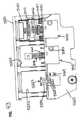
図2は、PLM機能と共にPLI機能を含む通信管理システム200の1つの例としての実施形態のブロック図である。管理システム200は、複数のコネクタアセンブリ202を備える。システム200は、IPネットワーク218に接続されている1つまたは2つ以上のコネクタアセンブリ202を含む。図2に示されているコネクタアセンブリ202は、図1のコネクタアセンブリ130の種々の実施形態を例示している。 FIG. 2 is a block diagram of an example embodiment of a
各コネクタアセンブリ202は、1つまたは2つ以上のポート204を含み、各ポートは、2つまたは3つ以上の物理通信メディアのセグメントを相互に接続するために使用される(例えば、図1の通信信号S1用の論理通信リンクの部分を実現するため)。少なくとも幾つかのコネクタアセンブリ202は、物理通信メディアのセグメントと共に使用されるように設計され、物理通信メディアのセグメントはその中、またはその上に物理層情報を有している。物理層情報は、格納されている情報が、セグメントがポート204に取り付けられているときに、コネクタアセンブリ202に関連するプログラマブルプロセッサ206が読むことを可能にする方法で、物理通信メディアのセグメントの中、または上に格納されている。 Each connector assembly 202 includes one or
図2に示されている特別な実施形態においては、コネクタアセンブリ202のポート204のそれぞれはメディア読取りインタフェース208をそれぞれ備え、メディア読取りインタフェース208を介して、各プログラマブルプロセッサ206は、物理通信メディアセグメントがそのポート204に取り付けられているかを判定することが可能であり、そして取り付けられていれば、取り付けられているセグメントの中、または上に格納されている物理層情報を読むことが可能である(そのようなメディア情報がその中、または上に格納されていれば)。各コネクタアセンブリ202に関連するプログラマブルプロセッサ206は、適切なバスまたは他の相互接続(図示せず)を使用して、各メディア読取りインタフェース208に通信可能に結合されている。 In the particular embodiment shown in FIG. 2, each of the
図2に示されている特別な実施形態においては、コネクタアセンブリ構成の4タイプの例が示されている。図2に示されている第1コネクタアセンブリ構成210においては、各コネクタアセンブリ202は、自身の各プログラマブルプロセッサ206と、このコネクタアセンブリ202をインターネットプロトコル(IP)ネットワーク218に通信可能に結合するために使用される、自身の各ネットワークインタフェース216を含む。 In the particular embodiment shown in FIG. 2, four types of examples of connector assembly configurations are shown. In the first connector assembly configuration 210 shown in FIG. 2, each connector assembly 202 is communicatively coupled to its respective
第2のタイプのコネクタアセンブリ構成212においては、コネクタアセンブリ202のグループが、物理的に相互に近接して位置している(例えば、ベイまたは機器クローゼットにおいて)。グループの中の各コネクタアセンブリ202は、自身の各プログラマブルプロセッサ206を含む。しかし、第2コネクタアセンブリ構成212においては、幾つかのコネクタアセンブリ202(ここでは、「インタフェース化コネクタアセンブリ」と称される)は、自身の各ネットワークインタフェース216を含むが、幾つかのコネクタアセンブリ202(ここでは、「非インタフェース化コネクタアセンブリ」と称される)は含まない。非インタフェース化コネクタアセンブリ202は、ローカル接続を介して、グループの中のインタフェース化コネクタアセンブリ202の1つまたは2つ以上と通信可能に結合されている。このようにして、非インタフェース化コネクタアセンブリ202は、グループの中の、1つまたは2つ以上のインタフェース化コネクタアセンブリ202に含まれるネットワークインタフェース216を介して、IPネットワーク218に通信可能に結合されている。第2のタイプのコネクタアセンブリ構成212においては、コネクタアセンブリ202をIPネットワーク218に結合するために使用されるネットワークインタフェース216の総数を削減可能である。更に、図2に示されている特別な実施形態においては、非インタフェース化コネクタアセンブリ202は、デイジーチェーントポロジ(他の実施形態と実施の形態においては他のトポロジを使用可能であるが)を使用して、インタフェース化コネクタアセンブリ202に接続されている。 In the second type of
第3のタイプのコネクタアセンブリ構成214においては、コネクタアセンブリ202のグループが、物理的に相互に近接して位置している(例えば、ベイ、または機器クローゼット内に)。グループの中の幾つかのコネクタアセンブリ202(ここでは、「マスター」コネクタアセンブリ202とも称される)は、自身のプログラマブルプロセッサ206とネットワークインタフェース216の両者を含むが、幾つかのコネクタアセンブリ202(ここでは、「スレーブ」コネクタアセンブリ202とも称される)は、自身のプログラマブルプロセッサ206もネットワークインタフェース216も含まない。各スレーブコネクタアセンブリ202は、1つまたは2つ以上のローカル接続を介して、グループの中の1つまたは2つ以上ののマスターコネクタアセンブリ202に通信可能に結合されている。各マスターコネクタアセンブリ202のプログラマブルプロセッサ206は、それ自身が一部であるマスターコネクタアセンブリ202と、ローカル接続を介してマスターコネクタアセンブリ202が接続されている任意のスレーブコネクタアセンブリ202の両者に対して、PLM機能を実行可能である。結果として、スレーブコネクタアセンブリ202に関連するコストを削減可能である。図2に示されている特別な実施形態においては、スレーブコネクタアセンブリ202は、スタートポロジ(他の実施形態と実施の形態においては他のトポロジを使用可能であるが)で、マスターコネクタアセンブリ202に接続されている。 In a third type of connector assembly configuration 214, groups of connector assemblies 202 are physically located in close proximity to each other (eg, in a bay or equipment closet). Some connector assemblies 202 in the group (also referred to herein as “master” connector assemblies 202) include both their own
各プログラマブルプロセッサ206は、プログラマブルプロセッサ206に下記に記述する種々の機能を実行させるソフトウェアまたはファームウェアを実行するように構成されている。各プログラマブルプロセッサ206はまた、プログラム命令とデータを格納するためにプログラマブルプロセッサ206に結合されている適切なメモリ(図示せず)も含む。一般的に、プログラマブルプロセッサ206は、プロセッサ206が関連するポート204に、物理通信メディアセグメントが取り付けられているかを判定し、取り付けられていれば、関連するメディア読取りインタフェース208を使用して、取り付けられている物理通信メディアセグメントの中、または上に格納されている識別子と属性情報を読む(セグメントが、その中、またはその上に格納されているそのような情報を含んでいれば)。 Each
第4のタイプのコネクタアセンブリ構成215においては、コネクタアセンブリ202のグループが、共通のシャーシまたは他のエンクロージャ内に収納されている。構成215の中の各コネクタアセンブリ202は、自身のプログラマブルプロセッサ206を含む。この構成215においては、各コネクタアセンブリの中のプログラマブルプロセッサ206は、「スレーブ」プロセッサ206である。各スレーブプログラマブルプロセッサ206もまた、共通の「マスター」プログラマブルプロセッサ217に通信可能に結合されている(例えば、シャーシまたはエンクロージャに含まれているバックプレーン上で)。マスタープログラマブルプロセッサ217は、プログラマブルプロセッサ217をIPネットワーク218に通信可能に結合するために使用されるネットワークインタフェース216に結合されている。 In a fourth type of connector assembly configuration 215, a group of connector assemblies 202 are housed in a common chassis or other enclosure. Each connector assembly 202 in configuration 215 includes its own
この構成215においては、各スレーブプログラマブルプロセッサ206は、物理通信メディアセグメントが、自身のポート204に取り付けられているかを判定し、取り付けられている物理通信メディアセグメントの中、または上に格納されている物理層情報を、関連するメディア読取りインタフェース208を使用して読むように構成されている(取り付けられているセグメントが、その中、またはその上に格納されているそのような情報を有していれば)。物理層情報は、シャーシの中の各コネクタアセンブリ202におけるスレーブプログラマブルプロセッサ206から、マスタープロセッサ217へ通信される。マスタープロセッサ217は、スレーブプロセッサ206により読まれた物理層情報を、IPネットワーク218に結合されている装置に通信することに関連する処理を取り扱うように構成されている。 In this configuration 215, each slave
システム200は、コネクタアセンブリ202が捕捉した物理層情報を、従来の物理層管理アプリケーション領域の外側のアプリケーション層機能による使用を可能にする機能を含む。つまり、物理層情報は、PLMの目的のみに使用されるPLM「島」には保持されず、他のアプリケーションに対して利用可能にされている。図2に示されている特別な実施形態においては、管理システム200は、IPネットワーク218を介してコネクタアセンブリ202に通信可能に結合されている集合点220を含む。
集合点220は、コネクタアセンブリ202(および他の装置)から物理層情報を得て、物理層情報をデータ記憶装置に格納する機能を含む。集合点200は、物理通信メディアのセグメントの中、または上に格納されている情報を自動的に読む機能を有している種々のタイプのコネクタアセンブリ202から物理層情報を受信するために使用可能である。また、集合点220と集合機能224は、物理通信メディアのセグメントの中、または上に格納されている情報を自動的に読む機能を有している他のタイプの装置から物理層情報を受信するために使用可能である。そのような装置の例は、コンピュータのようなエンドユーザー装置、周辺機器(例えば、プリンタ、コピー機、記憶装置、およびスキャナー)、およびIP電話などを含み、これらの装置は、物理通信メディアのセグメントの中、または上に格納されている情報を自動的に読む機能を含む。 Aggregation point 220 includes the ability to obtain physical layer information from connector assembly 202 (and other devices) and store the physical layer information in a data storage device.
集合点220または、他のタイプの物理層情報を得るためにも使用可能である。例えば、この実施形態においては、集合点220はまた、他の方法では集合点220に自動的には通信されない、物理通信メディアセグメントについての情報も得る。この情報は、例えば、そのような情報を、種々の機器のそれぞれの初期設置に関連して、手動でファイル(例えば、スプレッドシート)に入力して、集合点220にアップロード(例えば、ウェブブラウザを使用して)することにより集合点220に提供可能である。そのような情報はまた、例えば、集合点220により提供されるユーザーインタフェースを使用して直接に入力可能である(例えば、ウェブブラウザを使用して)。 It can also be used to obtain the aggregation point 220 or other types of physical layer information. For example, in this embodiment, the collection point 220 also obtains information about physical communication media segments that are not otherwise automatically communicated to the collection point 220. This information can be, for example, manually entered into a file (eg, a spreadsheet) and uploaded to the aggregation point 220 (eg, a web browser) in connection with the initial installation of each of the various devices. Can be provided to the collection point 220. Such information can also be entered directly using, for example, a user interface provided by the collection point 220 (eg, using a web browser).
集合点220はまた、外部装置またはエンティティが、集合点220により維持されている物理層情報へアクセスするためのインタフェースを提供する機能も含む。このアクセスは、情報を集合点220に供給することと共に、集合点220から情報を検索することを含むことが可能である。この実施形態においては、集合点220は、そのような外部装置とエンティティに、アクセスポイント220により維持されているPLIへの透明かつ便利なアクセスを提供可能な「ミドルウェア」として実現されている。集合点220は、IPネットワーク218上の該当する装置からPLIを統合し、外部装置およびエンティティにそのようなPLIへのアクセスを提供するので、外部装置およびエンティティは、PLIを提供するIPネットワーク218における装置のすべてと個々に相互作用する必要はなく、そのような装置は、そのような外部装置およびエンティティからの要求に応えるための容量を有する必要もない。 Aggregation point 220 also includes functionality that provides an interface for external devices or entities to access physical layer information maintained by aggregation point 220. This access can include retrieving information from the collection point 220 as well as providing information to the collection point 220. In this embodiment, the collection point 220 is implemented as “middleware” that can provide such external devices and entities with transparent and convenient access to the PLI maintained by the access point 220. Aggregation point 220 integrates PLI from appropriate devices on IP network 218 and provides external devices and entities with access to such PLI, so that external devices and entities in IP network 218 that provide PLI. There is no need to interact individually with all of the devices, and such devices need not have the capacity to meet the demands from such external devices and entities.
例えば、図2において示されているように、ネットワーク管理システム(NMS)230は、集合点220から物理層情報を検索し、その物理層情報を、NMS230の他の部分へ、それらによる使用のために提供するように構成されているPLI機能232を含む。NMS230は、検索した物理層情報を使用して、1つまたは2つ以上のネットワーク管理機能を実行する。NMS230は、IPネットワーク218上で集合点220と通信する。 For example, as shown in FIG. 2, the network management system (NMS) 230 retrieves physical layer information from the aggregation point 220 and passes the physical layer information to other parts of the NMS 230 for use by them. Includes a
図2に示されているように、コンピュータ236上で実行されるアプリケーション234はまた、集合点220により実現されるAPIを使用して、集合点220により維持されているPLI情報にアクセス可能である(例えば、そのような情報を集合点220から検索し、および/または、そのような情報を集合点220に供給することが可能)。コンピュータ236はIPネットワーク218に結合され、IPネットワーク218上で集合点220にアクセスする。 As shown in FIG. 2, an application 234 running on computer 236 can also access PLI information maintained by aggregation point 220 using an API implemented by aggregation point 220. (For example, such information can be retrieved from the collection point 220 and / or such information can be provided to the collection point 220). Computer 236 is coupled to IP network 218 and accesses collection point 220 over IP network 218.
図2に示されている例においては、IPネットワーク218を実現するために使用される1つまたは2つ以上の相互ネットワーク接続装置238は、物理層情報(PLI)機能を含む。相互ネットワーク接続装置238のPLI機能240は、集合点220から物理層情報を検索し、検索された物理層情報を使用して、1つまたは2つ以上の相互ネットワーク接続機能を実行するように構成されている。相互ネットワーク接続機能の例に、相互ネットワーク接続装置において受信した通信トラフィックのルーティング、スイッチング、リピーティング、ブリッジング、およびグルーミングのような、レイヤー1、レイヤー2、およびレイヤー3(OSIモデルの)の相互ネットワーク接続機能を含む。 In the example shown in FIG. 2, one or more of the internetwork attachments 238 used to implement the IP network 218 includes physical layer information (PLI) functionality. The PLI function 240 of the internetwork connection device 238 is configured to retrieve physical layer information from the aggregation point 220 and use the retrieved physical layer information to perform one or more internetwork connection functions. Has been. Examples of internetwork connectivity functions include
集合点220は、スタンドアロンのネットワークノード(例えば、適切なソフトウェアを起動しているスタンドアロンのコンピュータ)上に実現可能であり、または他のネットワーク機能と統合可能である(例えば、要素管理システム、またはネットワーク管理システム、または他のネットワークサーバーまたはネットワーク要素と統合可能)。更に、集合点220の機能は、ネットワークにおける多数のノードおよび装置に配布可能であり、および/または、例えば、階層的な方法で実現可能である(例えば、集合点の多数のレベルで)。IPネットワーク218は、1つまたは2つ以上のローカルエリアネットワークおよび/またはワイドエリアネットワーク(例えば、インターネット)を含むことが可能である。結果として、集合点220、NMS230、およびコンピュータ236は、同一サイトに相互の装置として位置する必要がなく、またコネクタアセンブリ202または相互ネットワーク接続装置238として同一サイトに位置する必要もない。 Aggregation point 220 can be implemented on a stand-alone network node (eg, a stand-alone computer running appropriate software) or can be integrated with other network functions (eg, element management system or network). Integrate with management systems or other network servers or network elements). Further, the function of the collection point 220 can be distributed to multiple nodes and devices in the network and / or can be implemented, for example, in a hierarchical manner (eg, at multiple levels of collection points). The IP network 218 may include one or more local area networks and / or wide area networks (eg, the Internet). As a result, the collection point 220, NMS 230, and computer 236 need not be located as mutual devices at the same site, and need not be located at the same site as the connector assembly 202 or the mutual network connection device 238.
また、電力は、IEEE802.3af標準において規定されている、従来の「Power over Ethernet(登録商標)(PoE)」技術を使用してコネクタアセンブリ202に供給可能であり、その技術は、ここに参照により組み込まれる。そのような実施形態においては、パワーハブ242または他の電力供給装置(各コネクタアセンブリ202に結合されている相互ネットワーク接続装置に近接して位置し、または相互ネットワーク接続装置内に統合されている)が、DCパワーを、各コネクタアセンブリ202を関連する相互ネットワーク接続装置238に接続するために使用される銅ツイストペアケーブルに含まれている、1つまたは2つ以上のワイヤ(ここでは、「パワーワイヤ」とも称される)上に注入する。 Also, power can be supplied to the connector assembly 202 using conventional “Power over Ethernet (PoE)” technology as defined in the IEEE 802.3af standard, which technology is referenced here. Is incorporated by In such an embodiment, a
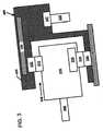
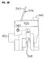
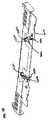
図3は、コネクタ装置310から物理層情報を収集するように構成されているコネクタアセンブリ320を含んでいる1つの例としての接続システム300の模式図である。示されている例としての接続システム300は、ジャックモジュール320と電気プラグ310を含む。コネクタ装置310は、物理通信メディアの少なくとも第1電気セグメント(例えば、コンダクタケーブル)305を終端し、コネクタアセンブリ320は、物理通信メディアの少なくとも第2電気セグメント(例えば、銅ワイヤのツイストペア)329を終端する。コネクタアセンブリ320は、コネクタ装置310を収容可能な少なくとも1つのソケットポート325を画定している。 FIG. 3 is a schematic diagram of an
コネクタ装置310の各電気セグメント305は、通信信号(例えば、図1の通信信号S1)を、コネクタ装置310上の一次接触子部材312に搬送する。コネクタアセンブリ320は、ソケットポート325からアクセス可能な一次接触子装置322を含む。一次接触子装置322は、一次接触子部材312に整列し、一次接触子部材312とのインタフェースを取るように構成されており、コネクタ装置310がコネクタアセンブリ320のソケット325内に挿入されているときに、一次接触子部材312から通信信号(図1のS1)を受信する。 Each
コネクタアセンブリ320は、1つまたは2つ以上のプリント回路基板に電気的に結合されている。例えば、コネクタアセンブリ320は、第1プリント回路基板326を支持または囲むことが可能で、第1プリント回路基板326は、絶縁変位接触子(IDC)327または他のタイプの電気接触子に接続する。IDC327は、物理通信メディア(例えば、伝導性ワイヤ)の電気セグメント329を終端する。第1プリント回路基板326は、ケーブル305を終端するコンダクタから、IDC327に結合されている電気セグメント329に搬送される一次通信信号を管理する。
幾つかの態様によれば、コネクタ装置310は、物理層情報を格納するように構成されている記憶装置315を含むことが可能である。コネクタ装置310はまた、記憶装置315に電気的に結合されている(または、通信可能に結合されている)第2接触子部材314も含む。1つの実施形態においては、記憶装置315は、EEPROM(例えば、PCB表面実装EEPROM)を使用して実現される。他の実施形態においては、記憶装置315は、他の不揮発性メモリ装置を使用して実現される。各記憶装置315は、メディアセグメント305上で通信される通信信号と干渉せず、または通信信号と相互作用しないように配置され且つ構成されている。 According to some aspects, the
コネクタアセンブリ320はまた、第2接触子装置(例えば、メディア読取りインタフェース324)も含む。ある実施形態においては、メディア読取りインタフェース324は、ソケットポート325を通してアクセス可能である。第2接触子装置324は、コネクタ装置310がコネクタアセンブリ320のソケット325に挿入されているときは、メディアセグメントの第2接触子装置324と整列して、第2接触子装置324とのインタフェースを取るように構成されており、記憶装置315から物理層情報を受信する。
幾つかのそのような実施形態においては、記憶装置インタフェース314とメディア読取りインタフェース324はそれぞれ、3本のリード線、つまり、パワーリード線、接地リード線、およびデータリード線を備えている。記憶装置インタフェース314の3本のリード線は、対応するメディアセグメントが対応するポート325に挿入されているときは、メディア読取りインタフェース324の対応する3本のリード線と電気的に接触する。ある例としての実施形態においては、2線インタフェースが、簡単なチャージポンプと共に使用される。更に他の実施形態においては、追加的リード線を設けることが可能である(例えば、可能性のある将来の適用のために)。従って、記憶装置インタフェース314とメディア読取りインタフェース324はそれぞれ、4本のリード線、5本のリード線、6本のリード線などを含んでもよい。 In some such embodiments, each of the
記憶装置315はまた、物理層情報用の記憶装置に加えて、プロセッサまたはマイクロコントローラも含んでもよい。幾つかの例としての実施形態においては、マイクロコントローラは、例えば、ケーブル305の完全性試験を行う(例えば、ケーブル305(そのような目的のために、金属箔または金属充填剤を含んでもよい)を取り囲む被覆材または絶縁体に対する容量またはインピーダンス試験を行うことにより)ソフトウェアまたはファームウェアを実行するために使用可能である。ケーブル305の完全性試験について問題が検出された場合は、マイクロコントローラは、その事実を、ポートに関連するプログラマブルプロセッサ(例えば、図2のプロセッサ206)に記憶装置インタフェースを使用して(例えば、インタラプトを発生して)通信可能である。マイクロコントローラはまた、他の機能のためにも使用可能である。 The
コネクタアセンブリ320はまた、第2プリント回路基板328を支持または囲むことが可能であり、第2プリント回路基板328は第2接触子装置324に接続する。第2プリント回路基板328は、第2接触子314、324を通して、記憶装置315から通信される物理層情報を管理する。示されている例においては、第2プリント回路基板328は、コネクタアセンブリ320の、第1プリント回路基板326とは反対側に位置している。他の実施形態においては、プリント回路基板326、328は、同じ側または異なる側に位置することが可能である。1つの実施形態においては、第2プリント回路基板328は、コネクタアセンブリ320に対して水平に位置している(図3参照)。他の実施形態においては、第2プリント回路基板328は、コネクタアセンブリ320に対して垂直に位置している。 The
第2プリント回路基板328は、1つまたは2つ以上のプログラマブル電子プロセッサおよび/または、1つまたは2つ以上のネットワークインタフェースに通信可能に接続可能である。1つの実施形態においては、1つまたは2つ以上のそのようなプロセッサとインタフェースは、第2プリント回路基板328上の構成要素として配置可能である。他の実施形態においては、1つまたは2つ以上のそのようなプロセッサとインタフェースは、第2プリント回路基板328に結合されている別の回路基板上に配置可能である。例えば、第2プリント回路基板328は、カードエッジタイプ接続、コネクタ・ツー・コネクタタイプ接続、ケーブル接続などを介して他の回路基板に結合可能である。ネットワークインタフェースは、物理層情報をデータネットワークに送るように構成されている(例えば、図1の信号S2参照)。 The second printed circuit board 328 is communicatively connectable to one or more programmable electronic processors and / or one or more network interfaces. In one embodiment, one or more such processors and interfaces can be arranged as components on the second printed circuit board 328. In other embodiments, one or more such processors and interfaces can be located on another circuit board that is coupled to the second printed circuit board 328. For example, the second printed circuit board 328 can be coupled to other circuit boards via card edge type connections, connector-to-connector type connections, cable connections, and the like. The network interface is configured to send physical layer information to the data network (see, for example, signal S2 in FIG. 1).
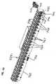
図4〜78は、電気(例えば、銅)通信アプリケーション用の物理層管理ネットワークと構成要素の例としての実施形態を提供する。図4〜14は、電気通信ケーブル5090を終端するためのモジュラープラグ5002の形状のコネクタ装置5000の例を示している。コネクタ装置5000は、ここで更に詳細に記述するように、コネクタアセンブリのポート内に受け入れられるように構成されている。1つの態様によれば、コネクタ装置5000は、RJプラグのようなプラグ5002を含み、プラグ5002は、ツイストペア銅ケーブル5090のような、通信メディアの電気セグメントの端部に接続する。 4 through 78 provide example embodiments of physical layer management networks and components for electrical (eg, copper) communication applications. 4-14 show an example of a
プラグ5002は、ツイストワイヤペアとストレインレリーフ(変形防止用)ブート5010を管理するためのワイヤマネージャ5008を含み、ワイヤマネージャ5008は、プラグ5002にスナップ嵌合されている(図4および5参照)。例えば、プラグ5002は開口部5005を画定しており、開口部5005において、ワイヤマネージャ5008上のラグ(突起部)5009がラッチ可能である(図13参照)。図12〜14は、プラグ5002との使用に適している1つの例としてのワイヤマネージャ5008とブート5010の詳細を示している。示されている例においては、ワイヤマネージャ5008とブート5010は一体的に形成されている。ワイヤマネージャ5008の第1部分5008Aは、一体丁番により、第2部分5008Bに接続されている。しかし、他の実施形態においては、他のタイプのワイヤマネージャとブートを利用してもよい。 The
プラグ5002はまた、第1側部5014と第2側部5016を有するプラグノーズ本体部5004も含む(図6〜11)。1つの実施形態においては、シールド5003をプラグノーズ本体部5004に搭載可能である。例えば、シールド5003をプラグノーズ本体部5004にスナップ嵌合可能である。プラグノーズ本体部5004の第1側部5014は、キー部材5015と、キー部材5015から外側に向けて延伸しているフィンガータブ5050を含む。キー部材5015とフィンガータブ5050は、ここで更に詳細に記述されるように、コネクタ装置5000の、コネクタアセンブリへの整列および固定を容易にする。ある実施形態においては、フィンガータブ5050は、キー部材5015においてプラグノーズ本体部5004に取り付けられる。1つの実施形態においては、フィンガータブ5050とキー部材5015は、プラグノーズ本体部5004と一体である。
フィンガータブ5050は十分に弾力性があり、フィンガータブ5050の末端部5051が撓曲し、プラグノーズ本体部5004に向けて、およびプラグノーズ本体部5004から遠ざかるように回転することを可能にする。あるタイプのフィンガータブ5050は、ここで更に詳細に記述されるように、少なくとも1つのカムフォローワ表面5052と、コネクタアセンブリへのラッチのためのラッチ表面5054を含む。ある実施形態においては、フィンガータブ5050は、ハンドル延長部5053のいずれの側にも位置する2つのカムフォローワ表面5052を含む(図6参照)。ハンドル延長部5053を押すと、ラッチ表面5054がプラグノーズ本体部5004に向けて移動する。ある実施形態においては、ワイヤマネージャ5008および/またはブート5010は、ハンドル延長部5053の少なくとも末端部5051上で曲がっており、ハンドル延長部5053の押下を容易にする柔軟性グリップ表面5011を含む(図4参照)。 The
プラグノーズ本体部5004の第2側部5016は、主要信号接触子5012を保持するように構成されており、主要信号接触子5012は、通信ケーブルのツイストペアコンダクタに電気的に接続されている。リブ5013は主要信号接触子5012を保護している。示されている例においては、プラグ5002は、図3のジャックモジュール320のポート325のような、コネクタアセンブリの合わせジャックのポート内に挿入可能である。プラグ5002の主要信号接触子5012は、ジャックモジュールに位置している接触子に電気的に接続し、図1の信号S1のような通信信号が搬送される電気経路を作成する。しかし、他の態様によれば、コネクタ装置5000は、他のタイプの電気接続を画定可能である。 The
幾つかの実施形態においては、プラグノーズ本体部5004のキー部材5015はキャビティ5060を画定している(図6参照)。幾つかの態様によれば、キー部材5015は、プラグノーズ本体部5004の前部に位置している。示されている例においては、キー部材5015は、フィンガータブ5050のベース5052を形成している。キー部材5015は、ハウジング部材5015の内部側にガイド溝5017を画定している支持部材5016を含む。 In some embodiments, the
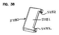
コネクタ装置5000はまた、物理通信メディアのセグメント(例えば、プラグ5002および/または、プラグ5002で終端されている電気ケーブル)に関する情報(例えば、識別子および/または属性情報)を格納するように構成されている記憶装置5030(図7)も含む。幾つかの実施の形態においては、コネクタ装置5000はまた、物理層管理において支援する追加的構成要素を含むことも可能である。幾つかの実施の形態においては、記憶装置5030は、モジュラープラグ5002に搭載されているプリント回路基板5020上に配置可能である(図8〜9参照)。示されている例においては、プリント回路基板5020は、ハウジング部材5015により画定されているキャビティ5060内のガイド溝5017に沿ってスライド可能である。ある実施の形態においては、追加的構成要素はプリント回路基板5020上に配置可能である。
図6〜7に示されている例においては、プリント回路基板5020は、接触子とランドを電気的に接続している伝導性トレースを備える基板を含む。回路5020はまた、メディア記憶装置を含んでいる回路構成要素もランドにおいて含む。図7に示されている例においては、回路5020はEEPROM5032を含む。1つの実施の形態においては、EEPROM5032は、モジュラープラグ5002用のメディア記憶装置5030を形成している。しかし、他の実施の形態においては、記憶装置5030は、任意の適切なタイプのメモリを含むことが可能である。 In the example shown in FIGS. 6-7, the printed
幾つかの態様によれば、回路5020は、第1側部5021と第2側部5023を有する本体部5022を画定している。EEPROM5032は、PCB本体部5022の第2側部5023に搭載可能である。回路接触子5034は、PCB本体部5022の第1側部5023上に配置されている。回路接触子5034により、EEPROM5032の、図3のメディア読取りインタフェース324のような、メディア読取りインタフェースへの接続が可能になる。 According to some aspects, the
プラグ5002はまた、プラグノーズ本体部5004上に搭載されているプラグカバー5006も含む(図8〜9参照)。示されている例においては、プラグカバー5006はハウジング部材5015に搭載されて、キャビティ5060を囲んでいる。例えば、プラグカバー5006は、第1側部5042と第2側部5044を画定している本体部5040を含む。示されている例においては、第1側部5042は、第2側部5044に対して略直交している。リブ5046は、第1および第2側部5042、5044の間で延伸している。示されている例においては、リブ5046は、第1および第2側部5042、5044により画定されている曲線状エッジ上で延伸している。1つの例においては、パッチパネル上のメディア読取りインタフェースの接触子は、リブ5046を通して延伸して、プリント回路基板5020上の回路接触子5034に接続可能である。 The
プラグカバー5006の本体部5040は、ハウジング部材5015において画定されているキャビティ5060内でラッチするように構成されているラッチアーム5007を画定可能である。例えば、ラッチアーム5007は、キャビティ5060において画定されている支持部材5016の背後でラッチ可能である。示されている例においては、ラッチアーム5007は、キャビティ5060におけるガイド溝5017内に基板5020が搭載されているときは、プリント回路基板5020の下方で延伸するように構成されている。1つの実施形態においては、プリント回路基板5020がハウジング部材5015内に搭載されているときは、プラグカバー5006はハウジング部材5015に、略水平に嵌合している(図10〜11参照)。 The
幾つかの態様によれば、コネクタ装置は、キー部材5015を含むプラグ本体部5004を製作して、記憶装置5030を、キー部材5015のキャビティ5060内に搭載して、キャビティ5060をカバー部材5006で閉じることにより製造される。幾つかの実施形態においては、プラグ本体部5004を製作することは、キー部材5015において、キャビティ5060と共にプラグ本体部5004を成形することを含む。他の実施形態においては、プラグ本体部5004を製作することは、本体部5004をキー部材5015と共に成形し、続いて、キー部材5015の材料を除去し(例えば、切削、溶融、解体などで)、キャビティ5060を形成することを含む。 According to some aspects, the connector device manufactures the
幾つかの実施形態においては、記憶装置5030は、EEPROMチップ5032をプリント回路基板5020上に搭載することにより製造される。接触子5034もまたプリント回路基板5020に搭載され、プリント回路基板5020のトレーシングを介してEEPROMチップ5032に電気的に接続される。ある実施形態においては、EEPROM5032は、プリント回路基板の一方の側に搭載され、接触子5034は別の側(例えば、反対側)に搭載される。 In some embodiments, the
幾つかの実施形態においては、記憶装置5030をプラグキャビティ5060内に位置させることは、記憶装置5030を、キャビティ5060において形成されているガイド5017に沿ってスライドすることを含む。ある実施形態においては、記憶装置5030をキャビティ5060内に搭載することは、接触子パッド5034がプラグ本体部5004から外側に、EEPROM5032がプラグ本体部5004に向けて内側に面する状態で、記憶装置5030をキャビティ5060内に位置させることを含む。ある実施形態においては、プラグ5002のキャビティ5060を閉じることは、カバー部材5006をキー部材5015の内部表面にラッチすることを含む。 In some embodiments, positioning the
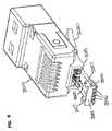
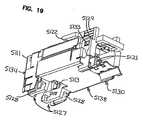
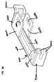
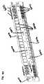
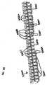
図15は、例としてのコネクタアセンブリ5100に挿入される、1つの例としてのコネクタ装置5000(例えば、プラグ5002)を示している。示されている例としてのコネクタアセンブリ5100は、プラグ5002を受け入れるように構成されているソケット5112を画定しているジャックモジュール5110を含む。1つの実施形態においては、ジャックモジュール5110はRJ−45ジャックソケット5112を含む。他の実施形態においては、ジャックモジュール5110は、他のタイプのジャックソケットを含んでもよい。 FIG. 15 illustrates one example connector device 5000 (eg, plug 5002) that is inserted into the
図16〜23は、ここで開示されるプラグ5002との使用に適している1つの例としてのジャックモジュール5110を例示している。ジャックモジュール5110はまたスロット5119も画定しており、スロット5119を通して、プラグ接続接触子5141がソケット5112内に延伸している。プラグ接続接触子5141は、プラグ接続接触子5141がプラグ5002の主要信号接触子5012に接触する接触子表面5142を画定している。ジャックモジュール5110は、プラグ5002がジャックモジュール5110内に挿入されるときに追従するソケット5112内のガイド表面5114を画定している(図17)。ガイド表面5114は、プラグ5002が挿入されるときにプラグ5002の前端部に接する、ソケット5112内の止め部表面5115に繋がっている。 FIGS. 16-23 illustrate one
あるタイプのジャックモジュール5110はまた、プラグ5002が挿入されているときに、プラグ5002をソケット5112内に保持するラッチング部材5116も含む(図17参照)。幾つかの実施形態においては、ラッチング部材5116は、カム表面5117を画定している第1端部と、肩部5118を画定している第2端部を有する(図19)。プラグ5002がソケット5112内に挿入されているときは、プラグ5002のフィンガータブ5050上のカムフォローワ表面5052は、ジャックモジュール5110のラッチング部材5116のカム表面5117上に乗っている。プラグ5002が十分に挿入されたときは、フィンガータブ5050のラッチ表面5054は、ジャックモジュール5110のラッチング部材5116の肩部5118の背後でスナップ嵌合する。 One type of
ラッチング部材5116はプラグ5002をソケット5112内に保持し、ソケット5112からのプラグ5002の不測の脱落を防止する。ソケット5112からプラグ5002を取り外すためには、ユーザーは、フィンガータブ5050のハンドル延長部5053を押して、フィンガータブ5050を、プラグノーズ本体部5004に向けて撓曲させればよい。例えば、ユーザーは、プラグ5002上の柔軟グリップ表面5011上を押せばよく、それにより、フィンガータブ5050のハンドル延長部5053が押される。フィンガータブ5050をプラグノーズ本体部5004に向け撓曲させると、ジャックモジュール5110のラッチング部材5116の肩部5118との整列から外れてラッチ表面5054が上昇し、それにより、ユーザーがプラグ5002をソケット5112から抜き出すことが可能になる。 The latching
あるタイプのジャックモジュール5110においては、ジャックモジュール5110のプラグ接続接触子5141は、ジャックモジュール5110のIDCセクション5121に位置している1つまたは2つ以上の絶縁変位接触子(IDC)5144に電気的に結合するように構成されている(図32参照)。プラグ5002をソケット5112に挿入すると、プラグ5002の主要信号接触子5012は、プラグ接続接触子5141の接触子表面5142に接触し、それにより、その間に電気的接続が確立される。プラグ5002で終端されているメディアセグメントにより搬送される信号は、ジャックモジュール5110のプラグ主要信号接触子5012を介して、IDC5144で終端されているメディアセグメントに転送されてもよい。しかし、他の実施形態においては、プラグ接続接触子5141は、他のジャックモジュールのプラグ接触子のような、他のタイプの接触子、または他の電気構成要素に接続してもよい。 In one type of
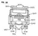
幾つかの実施形態においては、プラグ接続接触子5141は、IDC5144に直接接続する。例えば、1つの実施形態においては、プラグ接続接触子5141とIDC5144は一体接触子部材を形成してもよい。他の実施形態においては、プラグ接続接触子5141は、第1プリント回路基板5143を介してIDC5144に接続する。例えば、1つの実施形態においては、プラグ接続接触子5141とIDC5144は、半田ピンを使用して、または表面搭載接続を使用して、または他のタイプの接続を使用してプリント回路基板5143に接続してもよい(図32参照)。あるタイプのジャックモジュール5110は、第1プリント回路基板5143を支持するように構成されているシート(座部)5120を含む。図32に示されている例においては、第1プリント回路基板5143は、プラグ5002の挿入軸に平行な面において延伸している。 In some embodiments, the
幾つかの実施形態においては、ジャックモジュール5110はまた、ジャックモジュール5110における、第2電気ケーブルの保持を支援するストレインレリーフ(変形防止用)部材5110も含む。特に、ストレインレリーフ部材5130は、ジャックモジュール5110のIDC5144において終端されている電気コンダクタ(例えば、ワイヤ)を有する第2電気ケーブルの保持を支援する。あるタイプのストレインレリーフ部材5130は、ジャックモジュール5110に接続するラッチングタブ5133を有する少なくとも1つのアーム5132に接続されている支持表面5131を含む。図18、19および21に示されている例においては、例としてのストレインレリーフ部材5130は、それぞれがラッチングタブ5133を画定している2つのアーム5131間を延伸している曲面支持表面5131を含む。 In some embodiments, the
ジャックモジュール5110は、ストレインレリーフ部材5130のラッチングタブ5133がラッチしてもよい、少なくとも1つのリブ5129を画定している。示されている例においては、ジャックモジュール5110は、ジャックモジュール5110の各側において、複数のリブ5129を画定している。ストレインレリーフ装置5130は、ストレインレリーフ装置5130のタブ5133を適切なリブ5129にラッチすることにより、第2ケーブルの種々のタイプおよびサイズを収容するように調整してもよい。ある実施形態においては、ストレインレリーフ装置5130は、支持部材5131に加えられる外向きの圧力が、アーム5132をジャックモジュール5110の側に向けて撓曲するようにバネクリップを画定し、それにより、ストレインレリーフ装置5130がジャックモジュール5110に取り付けられる力が増大される。1つの実施形態においては、支持部材5131は、支持部材5131に対してのケーブルの保持を支援する、1つまたは2つ以上の突起部、切抜き、隆起部、または他の表面質感付与部材を画定している(例えば、図18参照)。 The
幾つかの実施形態においては、ジャックモジュール5110は、第1セクション5111に結合する第2セクション5138を含む。ある実施形態においては、第1セクション5111は、ソケット5112と、ラッチング部材5116と、IDCセクション5121と、を画定している。そのような実施形態においては、第2セクション5138は、第1セクション5111の少なくともIDCセクション5121を覆い、IDC5144におけるコンダクタの終端を保護してもよい。例えば、あるタイプの第2セクション5138は、IDCセクション5121全体に渡って延伸するベース5139と、ジャックモジュール5110の側上を延伸するアーム5140を含む(図16)。第2セクション5138のアーム5140は、ジャックモジュール5110の第1セクション5111をラッチまたは第1セクション5111に取り付けられてもよい。幾つかの実施形態においては、第1セクション5111は、ストレインレリーフ部材5130が取り付けられるリブ5129を画定している。しかし、他の実施形態においては、第2セクション5138は、リブ5129を画定してもよい。 In some embodiments, the
幾つかの実施形態においては、電気的伝導性シールド5134をジャックモジュール5110上に設置(例えば、スナップ嵌合、クリップ、ラッチなどで)してもよい(図7)。例えば、シールド5134を、ジャックモジュール5110と、ジャックモジュール5110において接続されている電気セグメントを接地するために使用してもよい。示されている例においては、伝導性シールド5134は、ジャックモジュール5110の第1側部上を延伸している第1セクション5135と、ジャックモジュール5110の側部上を延伸している側部セクション5136を含む。ある実施形態においては、シールド5134は、ジャックモジュール5110の前部を包み込み、少なくとも部分的にはソケット5112内に延伸しているラップアラウンドセクション5137を含む。ラップアラウンドセクション5137は、プラグ5002がジャックモジュール5110に挿入されているときは、プラグ5002のシールド5003と接触するように構成されている。1つの実施形態においては、ラップアラウンドセクション5137は、プラグシールド5003との接触を支援するための弾性セクションを画定している。 In some embodiments, an electrically
あるタイプのジャックモジュール5110は、ここで更に詳細に記述されるように、パッチパネルに搭載されるように構成されている。幾つかの実施形態においては、ジャックモジュール5110は、ジャックモジュール5110の、例としてのパッチパネルにおける設置を支援をするガイド5122を含む。図16〜23に示されている例においては、ガイド5122は、第1端部において傾斜またはカミング表面を有する翼部延長部を画定している。1つの実施形態においては、ジャックモジュール5110は、ジャックモジュール5110の各側から外側に向けて延伸しているガイド5122を含む(図20〜21)。1つの実施形態においては、ガイド5122は、ジャックモジュール5110の第1セクション5111上に形成されている。 One type of
あるタイプのジャックモジュール5110はまた、ジャックモジュール5110の、パッチパネルへの固定を支援するパネルラッチング装置5123も含む。幾つかの実施形態においては、パネルラッチング装置5123は、傾斜表面5124と肩部5125を有する第1ラッチ部材を少なくとも含む。示されている例においては、パネルラッチング装置5123は、ギャップ5126により分離されている2つのラッチ部材を含む。各ラッチ部材は、1つの端部において傾斜表面5124を画定し、反対側の端部において肩部5125を画定している。ある実施形態においては、ラッチ部材は、ガイド5122のほぼ間に位置している。ある実施形態においては、パネルラッチング装置5123は、ジャックモジュール5110の第1セクション5111上に位置している。 One type of
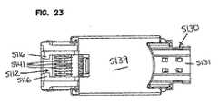
図15に戻って参照すると、コネクタアセンブリ5100はまた、ジャックモジュール5110に結合されているメディア読取りインタフェース5145(図24〜29)も含む。メディア読取りインタフェース5145は、プラグ5002(例えば、図30参照)の記憶装置接触子5034に接触して、記憶装置接触子5034と、図1のネットワーク101または図2のネットワーク218のようなデータネットワークの間の伝導性経路を提供するように構成されている第2接触子セット5146を含む。ある実施形態においては、第2接触子5146は、データネットワークに接続するように構成されている第2プリント回路基板5165(図32参照)に接続している(例えば、ここで記述されるようなプロセッサおよび/またはネットワークインタフェース)。 Referring back to FIG. 15, the
幾つかの態様によれば、メディア読取りインタフェース5145の第2接触子5146の少なくとも部分は、ジャックモジュール5110のソケット5112内に延伸している。幾つかの実施形態においては、第2接触子5146の部分は、ジャックモジュール5110の表面に画定されている切抜き5113を通して延伸してもよい(図31参照)。切抜き5113は、ジャックモジュール5110の壁を通しての、ジャックソケット5112へのアクセスを提供する。幾つかの実施形態においては、切抜き5113は、ジャックモジュール5110の前部においてソケットポートと連続している。ある実施形態においては、切抜き5113は、プラグ接続接触子5141がソケット5112内に延伸するときに通過する接触子スロット5119とは、ジャックモジュール5110の反対側において位置していてもよい(例えば、図15参照)。例えば、1つの実施形態においては、切抜き5113は、プラグ5002を固定するためのラッチング部材5116として、ジャックモジュール5110の同じ側に位置している(例えば、図31参照)。 According to some aspects, at least a portion of
あるタイプのジャックモジュール5110は、メディア読取りインタフェース5145の、ジャックモジュール5110への固定を支援するガイド部材5127(図16、19、および20参照)を含んでもよい。図16に示されている例においては、ガイド部材5127は、切抜き5113のいずれの側にも位置している。他の実施形態においては、ガイド部材5127は、ジャックモジュール5110上の他の場所に位置してもよい。幾つかの実施形態においては、ガイド部材5127は、メディア読取りインタフェース5145の部分を受け入れるように構成されているチャネル5128(図20)を画定している(図15参照)。 One type of
1つの例としてのメディア読取りインタフェース5145が図24〜29に示されている。例としてのメディア読取りインタフェース5145は、図16〜23に示されているジャックモジュール5110との使用に適している。メディア読取りインタフェース5145は、ジャックモジュール5110のガイド部材5127のチャネル5128に受け入れられるようにサイズと形状が決められているガイドフランジ5151(図24)を含む。1つの実施形態においては、ガイドフランジ5151は、メディア読取りインタフェース5145の、ジャックモジュール5110のガイド部材5127への固定を支援する止め部(例えば、隆起部)5152を含む(図24参照)。例えば、止め部5152は、ガイドフランジ5151の前方端部に画定されてもよい。 One example media read
幾つかの実施形態においては、メディア読取りインタフェース5145はまた、止め部装置5163も含む。図24に示されている例においては、止め部装置5163は、ガイドチャネルを止め部5163のいずれの側においてもガイドチャネルを画定している側方延伸翼部を含む、略U字形の上方延長部を画定している。幾つかの実施形態においては、メディア読取りインタフェース5145は、メディア読取りインタフェース5145のガイドフランジ5151を、ジャックモジュール5110のガイドチャネル5128内にスライドすることによりジャックモジュール5110に搭載される。ある実施形態においては、メディア読取りインタフェース5145の止め部5163は、メディア読取りインタフェース5145が挿入されているときは、ジャックモジュール5110のラッチング部材5116のカミング表面上に乗っている翼部を画定している。 In some embodiments, the media read
例としてのメディア読取りインタフェース5145はまた、データネットワークに接続する第2プリント回路基板5165を受け入れるように構成されているチャネル5150(図25と29)も含む。例えば、第2プリント回路基板5165は、プロセッサ(例えば、スレーブプロセッサまたはマスタープロセッサ)および/またはデータネットワークへの接続用のネットワークインタフェースに接続してもよい。ある実施形態においては、第2プリント回路基板5165は、プラブ5002の、ソケット5112内への挿入軸に略直交している面において延伸している。1つの実施形態においては、第2プリント回路基板5165は、第1プリント回路基板5143に略直交している面において延伸している。 The example media read
図26と27に示されているように、第2接触子5146は、プラグ接触子表面5147を画定している第1セクションから、PCB接触子表面5148を画定している第2セクションへ延伸している1つまたは2つ以上の接触子部材を含む。第2接触子5146のプラグ接触子表面5147は、メディア読取りインタフェース5145から出て延伸し、ジャックモジュール5110の切抜き5113を通り、ジャックソケット5112内に延伸している。PCB接触子表面はチャネル5150内に延伸して、第2プリント回路基板5165に接触している(図25参照)。ある実施形態においては、第2接触子5146の第2セクションはJ字形に曲がっており、PCB接触子表面5148を、チャネル5150内において、第2プリント回路基板5165と整列させている。 As shown in FIGS. 26 and 27, the
ある実施形態においては、メディア読取りインタフェース5145は、第1ハウジング部5156と第2ハウジング部5160を含む。第2接触子5146は、第1および第2ハウジング部5156、5160間に保持されている。幾つかの実施形態においては、第2プリント回路基板5165用のチャネル5150は、第1ハウジング部5156に形成されている。他の実施形態においては、チャネル5150は第2ハウジング部5160に形成されている。更に他の実施形態においては、第1および第2ハウジング部5156、5160は協働してチャネル5150を形成している(例えば、図32参照)。幾つかの実施形態においては、第1ハウジング部5156は、PCBチャネル5150とメディア読取りインタフェース5145の外部の間の通路を形成しているビューイングチャネル5153を画定している。ビューイングチャネル5153は、第2プリント回路基板5165上に設置されている光インディケータ(例えば、LED)5169と整列するように構成されている(図42参照)。 In some embodiments, the media read
幾つかの実施形態においては、第1ハウジング部5156は主要ハウジングを形成し、第2ハウジング部5160は保持セクションを形成している。第1ハウジング部5156は、前部および後部フランジ間を延伸しているPCBチャネル5150を画定している。ビューイングチャネル5153は前部フランジを通して延伸している。後部フランジは、第2ハウジング部5160を受け入れてもよい通路5158を画定している。ある実施形態においては、ハウジング部5156、5160の1つは整列部材を画定し、ハウジング部5156、5160の他方は、メディア読取りインタフェース5145の組立てを支援する整列スロットを画定している(図26参照)。 In some embodiments, the
更に、ある実施形態においては、ハウジング部5156、5160の1つは、第2接触子5146の接触子部材を受け入れてもよいスロットを画定している。例えば、幾つかの実施形態においては、第1ハウジング部5156は、第2接触子5146の接触子部材を受け入れるスロット5157を画定している。実際、幾つかの実施形態においては、第2ハウジング部5160は、第2接触子5146の接触子部材の、間隔を空けての配置を支援し、接触子部材の接触を禁止するリブ5161を含む。第1ハウジング部5156のスロット5157は、第2ハウジング部5160のリブ5161間のチャネルと整列している。 Further, in some embodiments, one of the
幾つかの実施形態においては、第2接触子5146はバネ接触子を形成している。そのような幾つかの実施形態においては、第1セクションは、プラグ5002がプラグ接触子表面5147を押すときに、止め部5163に向けて撓曲するように構成されている。例えば、第1セクションは、リブ5161間に画定されているチャネルを通過してもよい。或る実施形態においては、止め部5163は、第2接触子5146に面している傾斜表面5164を画定している。傾斜表面5164は、プラグ5002がジャック5110内に挿入されるときに、第2接触子5146の撓曲を収容するように整形し、位置決めしてもよい。 In some embodiments, the
幾つかの実施形態においては、第2ハウジング部5160は第1ハウジング部5156をラッチするように構成されている。例えば、幾つかの実施形態においては、第2ハウジング部5160は、第1ハウジング部5156のラッチング凹部5159にラッチするように構成されている1つまたは2つ以上のラッチ部材5162を含む。1つの実施形態においては、各ラッチ部材5162は、傾斜表面と、反対側に面している肩部を画定している(図26〜27)。他の実施形態においては、ラッチ部材は第1ハウジング部5156上に画定され、ラッチング凹部は第2ハウジング部5160上に画定されてもよい。更に他の実施形態においては、第2ハウジング部5160は第1ハウジング部5156に固定されてもよい。 In some embodiments, the
幾つかの態様によれば、あるタイプのメディア読取りインタフェース5145は、プラグ5002が、ジャックモジュール5110のソケット5112に受け入れられたかの判定を支援するように構成されている。幾つかの実施形態においては、メディア読取りインタフェース5145は、第2接触子5146の少なくとも幾つかと相互作用する感知部材を含む。他の実施形態においては、メディア読取りインタフェース5145は、第2接触子5146の少なくとも2つの接触子部材に渡って延伸している短絡ピン5155を含む(図28と31参照)。 According to some aspects, one type of media read
第2接触子5146の接触子部材の少なくとも幾つかは、選択的に短絡ピン5155に接触するように構成されている短絡表面5149を画定している。短絡ピン5155は、接触子部材の短絡表面5149が短絡ピン5155に接触するときに、第2接触子5146の2つまたは3つ以上の接触子部材間で電気短絡を発生させる。第2プリント回路基板5165は、接触子部材同士が短絡されたかを判定するように構成されている。 At least some of the contact members of the
幾つかの実施形態においては、メディア読取りインタフェース5145は、短絡ピン5155を受け入れてもよいピン受入れ通路5145(図27〜29)を画定している。幾つかの実施形態においては、ピン受入れ通路5145は第1ハウジング部5156に画定されている。ある実施形態においては、通路5154は、第1ハウジング5156の2つの接触子部材スロット5157に渡って延伸している。他の実施形態においては、通路5154は、第1ハウジング部5156のすべての接触子部材スロット5157に渡って延伸している。更に他の実施形態においては、ピン受入れ通路5145は第2ハウジング部5160に画定されてもよい。 In some embodiments, the media read
図32に示されているように、プラグ5002が、ジャックモジュール5110のソケット5112に受け入れられるときは、主要信号接触子5012はプラグ接続接触子5141に接触し、記憶部材接触子5034は第2接触子のプラグ接触子表面5147に接触する。プラグ5002のキー部材5015は、第2接触子5146の第1セクションを下方に押す(図30参照)。第2接触子5146のプラグ接触子表面5147を押すことにより、短絡表面5149は短絡ピン5155から遠ざかるように引っ張られ(図32参照)、それにより、接触子部材間の電気短絡が解消される。 As shown in FIG. 32, when the
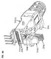
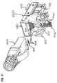
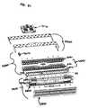
図33〜78を参照すると、幾つかの態様によれば、1つまたは2つ以上のジャックモジュール5110とメディア読取りインタフェース5145を共に結合してパッチパネルを形成可能である。一般的に、パッチパネルは、前部、後部、第1側部、および第2側部を有する。パッチパネルの前部は、電気ケーブルを終端するプラグ(例えば、図4〜14のプラグ5002)を受け入れる複数の前部ポートを画定している。パッチパネルの後部は、追加的な電気ケーブルを受け入れて終端してもよい複数の後部終端部を画定している。幾つかの実施形態においては、後部終端部は、絶縁変位接触子のような固定終端部を含む。例えば、ある実施形態においては、ジャックモジュール5110のソケット5112が前部ポートを画定し、ジャックモジュール5110のIDC5144が後部終端部を画定している。他の実施形態においては、後部終端部は追加的ジャックモジュールまたは他のタイプのコネクタを含んでもよい。 Referring to FIGS. 33-78, according to some aspects, one or
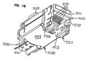
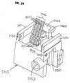
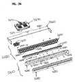
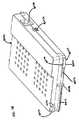
図33〜51は、前部5201、後部5202、第1側部5203、および第2側部5204を有する第1の例としてのパッチパネル5200を示している。パッチパネル5200は、少なくとも1つのジャックモジュール(例えば、図16〜23のジャックモジュール5110)と、少なくとも1つのメディア読取りインタフェース(例えば、図24〜29のメディア読取りインタフェース5145)を保持するように構成されている。第1の例としてのパッチパネル5200の前部5201は、1つまたは2つ以上の前部ポート5205を画定しており、前部ポート5205を通してジャックモジュールのソケットをアクセス可能である。第1の例としてのパッチパネル5200の後部5202は、ジャックモジュールのIDSセクション5121により画定される後部終端部を含む。 33 to 51 show a
パッチパネル5200は、パッチパネル5200の、ラック、フレーム、キャビネット、または他の機器構造物への設置を可能にするように構成されている搭載部材5206を含む。ある実施形態においては、搭載部材5206は、パッチパネル5200の側部5203、5204に位置している。示されている例においては、搭載部材5206は開口部5207を画定しており、開口部5207を通して、締結具(例えば、ネジ、ボルト、リベットなど)が延伸して、パッチパネル5200を1つまたは2つ以上のレールに固定してもよい。 The
幾つかの実施形態においては、パッチパネル5200は、前部ハウジング部5210と後部ハウジング部5220を含む(図34参照)。第1ハウジング部5210は前部ポート5205を画定している。幾つかの実施形態においては、前部ハウジング部5210はフレーム5240を含む。ある実施形態においては、前部ハウジング部5210はまた、フレーム5240に取外し可能に結合されているフェイシャ(fascia;カバー用帯体)5250も含む。ある実施形態においては、パッチパネル5200はまた、接地接続部5209(図35)も含む。接地接続部5209は、ジャックモジュール5110のシールド5134および/または第2プリント回路基板5165に接続してもよい。 In some embodiments, the
後部ハウジング部5220は、シャーシ5230に搭載されている少なくとも1つまたは2つ以上のジャックモジュール5110を含む。ある実施形態においては、後部ハウジング部5220はまた、1つまたは2つ以上のメディア読取りインタフェース5145も含む。1つの実施形態においては、パッチパネル5200は、同じ数のジャックモジュール5110とメディア読取りインタフェース5145を有する。他の実施形態においては、パッチパネル5200は、メディア読取りインタフェース5145より多くのジャックモジュール5110を含む。例えば、1つの実施形態においては、パッチパネル5200は、メディア読取りインタフェース5145の2倍の数のジャックモジュール5110を有してもよい。他の実施形態においては、パッチパネル5200は、ジャックモジュール5110よりも多くのメディア読取りインタフェース5145を含んでもよい。例えば、ある実施形態においては、各ジャックモジュール5110は2つのプラグソケットを画定してもよい。そのような実施形態においては、各プラグソケットは、自身のメディア読取りインタフェース5145を有してもよい。 The
幾つかの実施形態においては、メディア読取りインタフェース5145はプリント回路基板5165に搭載されている。図34に示されている例においては、メディア読取りインタフェース5145は、第2プリント回路基板5165の少なくとも第1エッジ上に搭載されている。各メディア読取りインタフェース5145もまた、少なくとも1つのジャックモジュール5110に接続されている。第2プリント回路基板5165はパッチパネル5200において設置されている。例えば、図34において、第2プリント回路基板5165は、第1ハウジング部5210と第2ハウジング部5220の間に保持されるように構成されている。 In some embodiments, media read
幾つかの実施形態においては、第1ハウジング部5210は第2ハウジング部5220に締結されている。示されている例においては、フレーム5240は、1つまたは2つ以上の第1開口部5212を画定し、第2プリント回路基板5165は、1つまたは2つ以上の第2開口部5222を画定し、シャーシ5230は、1つまたは2つ以上の第3開口部5224を画定している。1つまたは2つ以上の締結具(例えば、ネジ、ボルトなど)5215は、第1、第2、および第3開口部5212、5222、5224を通して延伸して、第2プリント回路基板5165を、フレーム5240とシャーシ5230の間に固定するように構成されている。ある実施形態においては、締結具5215は、フレーム5240と第2プリント回路基板5165の間に位置するスペーサ5218を通して延伸するように構成されている。 In some embodiments, the
示されている例においては、ネジ山付き締結具5212は、開口部5212、5222、5224を通して延伸するように構成されている。幾つかの実施形態においては、ネジ山付き締結具5212は、シャーシ5230内に直接ネジで固定されるように構成されている(例えば、シャーシ5230において画定されている通路5224内へ)。しかし、他の実施形態においては、ネジ山付き締結具5212は、ネジ山付き挿入物5225内にネジで固定されるように構成されている。そのような幾つかの実施形態においては、ネジ山付き挿入物5225は、シャーシ5230の後部からシャーシ5230の部分に接してもよい。例えば、ネジ山付き挿入物5225は、シャーシ5230に画定されている通路5224内で少なくとも部分的には搭載されてもよく、シャーシ5230の前方または中間表面に接してもよい。勿論、これらの取付け機構のいずれもが、ここで開示されるパッチパネルのいずれの構成要素上で使用可能である。 In the example shown, threaded fastener 5212 is configured to extend through
パッチパネル5200は、処理部(例えば、CPU)5270を受け入れるように構成されてもよい。一般的には、処理部5270は、少なくとも1つのプロセッサ(例えば、図2のプロセッサ206またはプロセッサ217)を含む。例えば、第2プリント回路基板5165は、処理部5270上のコネクタポートまたはコネクタ5271に接続するコネクタまたはコネクタポート(例えば、図57参照)を画定してもよい。第2プリント回路基板5165は、メディア読取りインタフェース5145を処理部5270へ電気的に接続する。従って、処理部5270は、1つまたは2つ以上のメディア読取りインタフェース5145に、1つまたは2つ以上の対応するプラグ5002の記憶装置5030から情報(例えば、物理層情報)を読むように要求してもよい。処理部5270はまた、メディア読取りインタフェース5145から情報を受信し、その情報をデータネットワーク(例えば、図1のネットワーク101または図2のネットワーク218)に提供してもよい。ある実施形態においては、処理部5270はまた、メディア読取りインタフェース5145を介して、情報を1つまたは2つ以上のプラグ5002の記憶装置5030に提供してもよい(例えば、書いてもよい)。
幾つかの実施形態においては、パッチパネル5200はまた、少なくとも1つのケーブルマネージャ5260を含んでもよい。ある実施形態においては、パッチパネル5200は、後部終端部に接続されているケーブルを組織化するケーブルマネージャ5260を含む。幾つかの実施形態においては、ケーブルマネージャ5260は第2ハウジング部5220に搭載される。例えば、1つの実施形態においては、ケーブルマネージャ5260はシャーシ5230に搭載される。他の実施形態においては、ケーブルマネージャは、シャーシ5230に搭載されている接地アセンブリ5209(図52参照)に搭載される。他の実施形態においては、ケーブルマネージャ5260は前部ハウジング部5210に搭載されてもよい。 In some embodiments, the
フレーム5240の1つの例としての実施形態が図34Bに示されている。フレーム5240は、少なくとも1つの開口部5242を画定しているフレーム本体部5241を含み、開口部5242を通して、プラグ5002は、ジャックモジュール5110のソケット5112にアクセス可能である。ある実施形態においては、開口部5242は十分に大きく、第1および第2ハウジング部5210、5220を共に搭載したときに、ジャックモジュール5110とメディア読取りインタフェース5145の両者の前部を、フレーム5240の前部から見えるようすることが可能である。例えば、メディア読取りインタフェース5145のビューイングチャネル5153は、フレーム開口部5242を通して見えるようにしてもよい。 One example embodiment of
ある実施形態においては、フレーム本体部5241は、第1および第2ハウジング部5210、5220の保持を支援する第2ハウジング部5220の部分を包む上部および下部撓曲フランジ5243を画定している。ある実施形態においては、下部フランジ5243は、第2プリント回路基板5165の、パッチパネル5200内での保持を支援してもよい。例えば、フレーム本体部5241の下部撓曲フランジ5243は、第2プリント回路基板5165の底部上を延伸して、第2メディア読取りインタフェースに画定されているチャネル5150内に第2回路基板5165を保持してもよい(例えば、図51参照)。 In certain embodiments, the
上記のように、フレーム本体部5241はまた開口部5212も画定しており、開口部5212を通して、締結具(例えば、ネジ、ボルト、リベットなど)5215が挿入されて、第1ハウジング部5210を第2ハウジング部5220に固定してもよい。幾つかの実施形態においては、フレーム本体部5241はまた、第2ハウジング部5220に搭載されている構成要素を収容するための開口部も画定している。例えば、フレーム本体部5241は、ここで更に詳細に記述されるように、ケーブルポート5166と光インディケータ5167を収容するための開口部5246、5247を画定してもよい。 As described above, the
幾つかの実施形態においては、フレーム本体部5241は搭載部材5206を画定している。例えば、フレーム5241の側部フランジは開口部5207を画定しており、開口部5207を通して、締結具を延伸させてもよい、他の実施形態においては、別の搭載部材5206がフレーム本体部5241に接続してもよい。他の実施形態においては、搭載部材5206はフェイシャ5250により画定されてもよい。更に他の実施形態においては、搭載部材5206は第2ハウジング部5220(例えば、シャーシ5230)に接続してもよい。 In some embodiments, the
フレーム本体部5241はまた、フェイシャ5250を受け入れるようにも構成されている。幾つかの実施形態においては、フレーム本体部5241は、フェイシャ5250の保持部材5258を受け入れるように構成されている開口部5244を画定している。他の実施形態においては、フレーム本体部5241は、フェイシャ5250に画定されている開口部に嵌入される保持部材を画定してもよい。ある実施形態においては、フレーム本体部5241はまた、開口部5242の幾つかから外側に延伸し、フェイシャ5250に画定されているスロットに受け入れられ、フレーム5240上のフェイシャ5250の整列および設置を支援するタブ5245も含む。 The
フェイシャ5250の1つの例としての実施形態が図34Aに示されている。フェイシャ5250は、フレーム本体部5241の開口部5242と整列して、パッチパネル5200の前部5201からジャックソケット5112へのアクセスを提供する複数の開口部5252を画定しているフェイシャ本体部5251を含む。幾つかの実施形態においては、フェイシャ本体部5251の開口部5252は、フレーム本体部5241の開口部5242よりも小さい。ある実施形態においては、フェイシャ本体部5251の開口部5252は、プラグ5002用のキー溝5253を画定している。フェイシャ本体部5251のキー溝5253は、第1および第2ハウジング部5210、5220が共に搭載されているときは、ジャックモジュール5110の切抜き5113と整列するような方向に向けられている。 One exemplary embodiment of the
幾つかの実施形態においては、フェイシャ本体部5251は、フェイシャ本体部5251から外側に向けて延伸しているタブ5254を含む。示されている例においては、タブ5254は開口部5252に略整列している。しかし、他の実施形態においては、フェイシャ本体部5251は、より多くの、またはより少ないタブ5254を含んでもよい。タブ5254は、フェイシャ5250がフレーム5240に搭載されているときは、フレーム本体部5241の上部および下部撓曲フランジ5243上を延伸している。1つの実施形態においては、タブ5254は、フレームのフランジ5243上で摩擦嵌合して、フェイシャ5250の、フレーム5240への保持を支援する。ある実施形態においては、幾つかのタブ5254は、フェイシャ5250の、フレーム5240への保持を支援してもよい開口部、切抜き5255、または内部突起部を画定している。 In some embodiments, the
上記のように、フェイシャ本体部5251はまた、フェイシャ本体部5251をフレーム本体部5241に固定する保持部材5258も含む。幾つかの実施形態においては、フェイシャ本体部5251は、フェイシャ本体部5251の各側部において少なくとも1つの保持部材5258を含む。他の実施形態においては、フェイシャ本体部5251は、フェイシャ本体部5251の各側部において複数の保持部材5258を含む。更に他の実施形態においては、フェイシャ本体部5251は、フェイシャ本体部5251の少なくとも1つの側部(例えば、底部)に沿って間隔を空けて配置されている複数の保持部材を含む。 As described above, the
幾つかの実施形態においては、保持部材5258はフレーム本体部5241を通して延伸して、開口部5244においてラッチする。他の実施形態においては、保持部材5258は、ラッチング開口部5244を介して、フレーム本体部5241へ固定(例えば、ラッチ、プレス嵌合、スナップ勘合などで)されてもよい。他の実施形態においては、保持部材5258は開口部5244を通して延伸して、第2ハウジング部5220のシャーシ5230に固定されてもよい。 In some embodiments, the retaining member 5258 extends through the
幾つかの実施形態においては、フェイシャ本体部5251はまた、第2ハウジング部5220に搭載されている構成要素を収容する開口部も画定している。例えば、フェイシャ本体部5251は、第2プリント回路基板5165のケーブルポート5166と光インディケータ5167を収容する開口部5256、5257、5259を画定してもよい。ケーブルポート5166と光インディケータ5167を含んでいるプリント回路基板5165の1つの例としての実施形態は、ここで更に詳細に記述される。 In some embodiments, the
図37〜39に示されているように、端部キャップ5280が、フレーム5241の側部フランジ上に搭載されて搭載部材5206を覆ってもよい。示されている例においては、各端部キャップ5280は、フレーム5241の1つの側部フランジの前部を覆うようにサイズと形状を決められている本体部5281を含む。各端部キャップ5280はまた搭載部材5282も含み、搭載部材5282により、端部キャップ本体部5281はパッチパネル5200に取り付けられている。幾つかの実施形態においては、搭載部材5282はフレーム本体部5241に取り付けられている。他の実施形態においては、搭載部材5282はフェイシャ本体部5251に取り付けられている。 As shown in FIGS. 37 to 39, an
あるタイプの端部キャップ5280は、搭載部材5206の開口部5207を選択的に露出および覆うために回転するように構成されている。幾つかの実施形態においては、搭載部材5282はピンを含み、ピンの回りを端部キャップ本体部5281が回転してもよい(図39)。図37に示されている例においては、搭載ピン5282はフェイシャ本体部5251の側部に取り付けられている。端部キャップ5280はまた保持機構5283(図39)も含み、保持機構5283により、端部キャップ本体部5281は定位置に保持されて、搭載部材開口部5207を覆ってもよい。保持機構5283は、端部キャップ5280が搭載部材5206を覆っているときは、搭載部材5206の部分5287(図37)を把持している。示されている例においては、保持機構5283は、搭載部材に画定されている切抜き5286を通して延伸しているフランジ5284とラッチングタブ5285を含む。ラッチングタブ5285は、搭載部材5206の部分5287の背後でスナップ嵌合している。 One type of
ラベルを、フェイシャ本体部5251上に設置してもよい。幾つかの実施形態においては、ラベルはフェイシャ本体部5251の前部上に設置される。例えば、ラベルを、フェイシャ本体部5251の前部へ接着、ラッチ、または固定してもよい。しかし、他の実施形態においては、ラベルを、透明または不透明フェイシャ本体部5251の背後に設置してもよい。ある実施形態においては、1つまたは2つ以上のラベルホルダ5290を、パッチパネル5200の第1部5210に搭載してもよい。 The label may be installed on the facer
1つの例としてのラベルホルダ5290が図40と41に示されている。例としてのラベルホルダ5290は、第1側部5298と第2側部5299を有するホルダ本体部5291を含む。ホルダ本体部5291の少なくとも第1側部5298は、上部および下部フランジ5293により境界を決められているトレー5292を画定している。1つまたは2つ以上のラベルを、フランジ5293間のトレー5292に設置してもよい。ある実施形態においては、保持タブ5296(図41)を、トレー5292内のラベルの保持を更に支援するために設けてもよい。ある実施形態においては、ラベルホルダ5290は、ホルダトレー5292のセクションを分離して、複数のラベルをトレー5292に並べて搭載することを容易にする分割フランジ5297(図41)を含んでもよい。 One
幾つかの実施形態においては、ラベルホルダ5290は、フレーム本体部5241とフェイシャ本体部5251の間に搭載されるように構成されている。例えば、ある実施形態においては、ホルダ本体部5291は、フレームとフェイシャ本体部5241、5251の間に保持されている第1取付け端部5294と第2取付け端部5295を含む(例えば、図36と36A参照)。示されている例においては、少なくとも第2取付け端部5295は、フェイシャ本体部5251の開口部5292を通して延伸するように構成されている(図36A参照)。 In some embodiments, the
あるタイプのラベルホルダ5290は反転可能に構成されている。例えば、図40〜41に示されているラベルホルダ5290は、トレー5292から前方と後方の両方に向けて延伸しているフランジ5293を含む。従って、ラベルを、ラベルホルダ5290のいずれの側部5298、5299に設置してもよい。1つの実施形態においては、ラベルホルダ5290の第1側部5298(図40)は、1つの細長いラベルを保持するように構成されており、ラベルホルダ5290の第2側部5299(図41)は、複数の短いラベルを保持するように構成されている。ホルダ本体部5291の第1および第2取付け端部5294、5295は、ラベルホルダ5290が、フェイシャ本体部5251を通して前方に面している第1側部5298または第2側部5299のいずれかにより、第1ハウジング部5210に固定されてもよいように構成されている。従って、ユーザーは、ラベルホルダ5290のいずれかの側部を選択してホルダラベルに利用してよい。 One type of
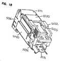
図42〜49は、第2ハウジング部5220の例としての構成要素を示している。図42は、第2プリント回路基板5165の第1エッジに搭載されている1つの例としての第2ハウジング部5220の前部透視図である。第2プリント回路基板5165の前部側は接触子パッド5168を画定しており、接触子パッド5168において、メディア読取りインタフェース5145の第2接触子5146が、第2回路基板5165に電気的に接続する(図43参照)。第2プリント回路基板5165の後部側は、処理ユニット5270のコネクタまたはコネクタポート5271(図34)へ結合するように構成されているコネクタまたはコネクタ5278(図57)を含む。 42 to 49 show constituent elements as examples of the
第2回路基板5165の前部側はまた、メディア読取りインタフェース5145、第2接触子5146、ジャックモジュール5110、および/またはプラグ接続接触子5141に関する情報を表示するために使用される光インディケータ(例えば、発光ダイオード)5169も含む(図43参照)。光は、メディア読取りインタフェース5145のビューイングチャネル5153を通して可視である。幾つかの実施形態においては、第2プリント回路基板5165はまた追加的な光インディケータ5167も含み、パッチパネルの状態についての情報をユーザーに提供してもよい(図42参照)。例えば、追加的光インディケータ5167はエラー情報を提供してもよい。図42に示されている例においては、第2プリント回路基板5165は3つの追加的光インディケータ5167を含む。しかし、他の実施形態においては、第2プリント回路基板5165は、より多くの、またはより少ない追加的光インディケータ5167を含んでもよい。 The front side of the
ある実施形態においては、第2回路基板5165はまたケーブルポート5166も含み、ケーブルポート5166において、ケーブルの、第2プリント回路基板5165とのインタフェースを取ってもよい(例えば、図42参照)。例えば、ケーブルポート5166は、ユーザーがデータケーブルを第2プリント回路基板5165に接続して、パッチパネル5200に挿入されている1つまたは2つ以上のプラグ5002上の記憶装置5030から情報を得ることを可能にしてもよい。ある実施形態においては、ケーブルポート5166はまた、ユーザーが、1つまたは2つ以上のプラグ5002の記憶装置5030に直接情報を書くことを可能にしてもよい。他の実施形態においては、ケーブルポート5166は、ユーザーが、パッチパネル5200の前部5201から処理ユニット5270へアクセスすることを可能にする。 In some embodiments, the
1つの例としてのシャーシ5230が図45〜48に示されている。シャーシ5230はシャーシ本体部5231を含み、シャーシ本体部5231は開口部5232を画定し、開口部5232を通して、ジャックモジュールはシャーシ本体部5231に搭載可能である。示されている例においては、シャーシ本体部5231は凹部5235(図45〜46)を画定しており、凹部5235を通して、処理ユニット5270は延伸して、第2プリント回路基板5165に接続してもよい。ある実施形態においては、シャーシ本体部5231は、各開口部5232内に延伸している搭載部材5233を含む(図43〜44)。示されている例においては、各搭載部材5233は、いずれの側においてもチャネル5234を画定している略T字形本体部を含む。各搭載部材5233は、開口部5232のジャックモジュール5110の1つの保持を支援するように構成されている。 One
ある実施形態においては、ジャックモジュール5110は、シャーシ本体部5231の後部側からシャーシ本体部5231上に設置される(例えば、図42参照)。ジャックモジュール5110は、搭載部材5233のいずれの側にも位置しているジャックモジュール5110のガイド部材5127(図17と19参照)により、開口部5232内にスライドする。1つの実施形態においては、ジャックモジュール5110のラッチング部材5116は、搭載部材5233により画定されているチャネル5234内でスライドする(図43〜44参照)。 In an embodiment, the
幾つかの実施形態においては、各メディア読取りインタフェース5145は、ジャックモジュール5110がシャーシ本体部5231に搭載された後に、対応するジャックモジュール5110に搭載される。他の実施形態においては、各メディア読取りインタフェース5145は第2プリント回路基板5165上に設置されて、基板装置5289を形成する(図49)。基板装置5289は、ジャックモジュール5110がシャーシ本体部5231に搭載される前または後に、シャーシ本体部5231に搭載可能である(例えば、図43参照)。 In some embodiments, each media read
幾つかの実施形態においては、シャーシ本体部5231は、ジャックモジュール5110の、シャーシ本体部5231への保持を支援する、1つまたは2つ以上のラッチング部材5236を含む。図47と48に示されている例としてのラッチング部材5236は、少なくとも1つの肩部5238を画定している柔軟タブ5237を含む。ある実施形態においては、各ラッチング部材5236は、柔軟タブ5237のそれぞれの側上に肩部5238を画定している。示されている例においては、各柔軟タブ5237は、マッシュルーム形をほぼ画定している。他の実施形態においては、各柔軟タブ5237は、T字形をほぼ画定している。 In some embodiments, the
ジャックモジュール5110がシャーシ本体部5231上に設置されているときは、ジャックモジュール5110の前端部は、シャーシ本体部5231の後部から、シャーシ本体部5231の開口部5232を通して挿入されている。ジャックモジュール5110が挿入されるときは、シャーシ本体部5231のラッチング部材5236の1つは、ジャックモジュール5110のラッチング部材5123の傾斜表面5124上でカミング動作(端面の振れ動作)を行う(図47参照)。ジャックモジュール5110がシャーシ5231に十分挿入されると、シャーシ本体部5231のラッチング部材5236は、ジャックモジュール5110のラッチング部材5123上方でスナップ嵌合し、それにより、シャーシラッチング部材5236の肩部5238は、ジャックラッチング部材5123の肩部5125に接する(図48参照)。 When the
図51は、組立パッチパネル5200内に挿入されている、例としてのプラグ5002の断面図を示す。プラグ5002は、フェイシャ開口部5252とフレーム開口部5242を通して、シャーシ5230に搭載されているジャックモジュール5110のソケット5112内に延伸している。プラグ5002の記憶部材接触子5034は、メディア読取りインタフェース5145の第2接触子5146を押して、第2接触子5146を短絡ピン5155から上昇させる。第2接触子5146に電気的に接続されている第2プリント回路基板5165は、第2接触子5146がピン5155により短絡されていないことを感知するように構成されている。 FIG. 51 shows a cross-sectional view of an
1つの例としての処理ユニット5270が図34Cに示されている。処理ユニット5270は、少なくとも第1コネクタ5271を含み、第1コネクタ5271により、処理ユニット5270は第2プリント回路基板5270に接続されてもよい。幾つかの態様によれば、あるタイプの処理ユニットは、処理ユニットのプリント回路基板5165への接続を容易にするガイドおよび/または保持部材を含む。例えば、処理ユニット5270は保持部材5274を含み、保持部材5274により、処理ユニット5270はパッチパネル5200に固定されてもよい。ある実施形態においては、保持部材5274は、ガイド部材5275と、少なくとも1つのラッチング部材5276と、押下表面5277と、を含む。示されている例においては、保持部材5274は、2つのラッチング部材5276を含む。 One
例としての処理ユニット5270はまた、電気ケーブル(例えば、パワーケーブル、データネットワークに接続されているデータケーブルなど)を受け入れるように構成されているポート(例えば、図35のポート5237参照)を含んでもよい。1つの実施形態においては、ポートはRJジャック(例えば、RJ−45ジャック)を含む。しかし、他の実施形態においては、処理ユニット5270は他のタイプのポートを利用してもよい。ある実施形態においては、処理ユニット5270はまた第2ポート(例えば、USBポート)も含み、第2ポートにおいて、他のタイプのケーブルが処理ユニット5270に接続されてもよい(例えば、図35のポート5273参照)。 The
図34と50は、パッチパネル5200との使用に適している1つの例としての支持部材5260を示す。支持部材5260は、パッチパネル5200に取り付けられるように構成されているアーム5262を有する本体部5261を含む。例えば、幾つかの実施形態においては、アーム5262は、パッチパネル5200の第2ハウジング部5220に取り付けてもよい(例えば、シャーシ5230へ)、他の実施形態においては、アーム5262は、パッチパネル5200に取り付けられている接地モジュール5209に取り付けてもよい(例えば、図52参照)。1つの実施形態においては、アーム5262は、支持部材5260の本体部5261と一体である。 34 and 50 show one
図34Cに示されているように、支持プレート5260の本体部5261は保持セクション5264を含み、保持セクション5264において、処理ユニット5270は支持プレート5260に固定されてもよい。例えば、幾つかの実施形態においては、支持プレート5260は、保持セクション5274においてスロット5265を画定し、スロット5265は、保持処理ユニット5270のガイド部材5275を受け入れるように構成されている。支持プレート5260の本体部5261はまた、処理ユニット5270の保持部材5274のラッチング部材5276を受け入れるように構成されている開口部またはスロット5266を画定してもよい。幾つかの実施形態においては、処理ユニット5270は、処理ユニット5270を支持プレート5260に対して前方にスライドさせることにより支持プレート5260にラッチされる。 As shown in FIG. 34C, the
幾つかの実施形態によれば、支持プレート5260はマネージャを画定している。そのような幾つかの実施形態においては、本体部5261は、1つまたは2つ以上のスロット5263を画定し、スロット5263において、ケーブル(例えば、ジャックモジュール5110において終端しているケーブル)は、ケーブル固定具または他の保持部材により固定可能である。他の実施形態においては、本体部5261は、1つまたは2つ以上の隆起タブを含んでもよく、隆起タブにおいて、ケーブル固定具または他の保持部材が締結されてもよい。例えば、適切なケーブルマネージャ本体部の1つの例としての実施形態が図55Eに示されており、ここで更に詳細に記述される。 According to some embodiments,
図52〜60は、他の例としてのフレーム5440に搭載される他の例としてのフェイシャ5450を含む、他の例としてのパッチパネル5400を示す。フレーム5440は他の例としてのシャーシ5430に固定されて、第2プリント回路基板5165に搭載されているメディア読取りインタフェース5145を囲んでいる。端部キャップ5480は、回転可能にシャーシ5450に搭載されて、フレーム5440の搭載セクションを覆っている。 FIGS. 52-60 illustrate another
パッチパネル5400への取付けに適切なプロセッサ(例えば、図2のプロセッサ206、217)を含む第2の例としての処理ユニット5470が図55に示されている。第2の例としての処理ユニット5470は、処理ユニット5470を第2プリント回路基板5165に接続する第1コネクタ5471を含む。第2処理ユニット5470はまた、電気ケーブル(例えば、パワーケーブル、データネットワークに接続されているデータケーブルなど)を受け入れるように構成されているポート5472も含む。1つの実施形態においては、ポート5472はRJジャック(例えば、RJ−45ジャック)を含む。しかし、他の実施形態においては、処理ユニット5470は他のタイプのポートを利用してもよい。ある実施形態においては、処理ユニット5470はまた第2ポート(例えば、USBポート)547’も含み、第2ポート547’において、他のタイプのケーブルが処理ユニット5470に接続されてもよい。 A second
図55に示されているように、処理ユニット5470はまた、処理ユニット5470の側部から外側に向けて延伸している保持部材5474を含んでもよい。幾つかの実施形態においては、保持部材5474は、処理ユニット5470の後端部に向けて位置している。他の実施形態においては、保持部材5474は、処理ユニット5470の側部に沿う中間位置に位置してもよい。各保持部材5474は、カミング表面5475と、少なくとも1つの保持タブ5476と、を画定している。示されている例においては、各ガイド部材5474は、上方に延伸している保持タブ5476と、下方に延伸している保持タブ5476を含む。 As shown in FIG. 55, the
処理ユニット5470はまた、処理ユニット5470の1つのまたは両方の側部上にガイド部材5477を含んでもよい。幾つかの実施形態においては、ガイド部材5477は、処理ユニット5470の前部と後部の間を少なくとも部分的には延伸している1つまたは2つ以上のレールを含む。ある実施形態においては、ガイド部材5477はまた、レールの端部において止め部5478も含む。示されている例においては、止め部5478は、処理ユニット5470の前部と後部の間の中間位置に位置している。止め部5478は、レール5477の端部から略直交して延伸している。1つの実施形態においては、ガイド部材5477はまた、前方止め部5479も含んでもよい。 The
パッチパネル5400との使用に適切な第2の例としてのケーブルマネージャ5460(図35参照)。ケーブルマネージャ5460は、パッチパネル5400に取り付けられている本体部5461を含む。マネージャ5460の本体部5461は、1つまたは2つ以上のスロット5463を画定し、スロット5463においてケーブル(例えば、ジャックモジュール5110で終端しているケーブル)は、ケーブル固定具または他の保持部材により固定可能である。幾つかの実施形態においては、マネージャ5460の本体部5461は、スロット5463の代わりに、またはスロット5463に追加して隆起タブを含んでもよい。 A second
幾つかの実施形態においては、パッチパネル5400に取り付けられるように構成されている2つのアーム5426の間で延伸している本体部5461。例えば、幾つかの実施形態においては、アーム5426は、パッチパネル5400の第2ハウジング部に取り付けてもよい(例えば、シャーシ5430へ)。他の実施形態においては、アーム5426は、パッチパネル5400に取り付けられている接地モジュール5409に取り付けてもよい(例えば、図52参照)。1つの実施形態においては、アーム5426は、ケーブルマネージャ5460の本体部5461と一体である。 In some embodiments, a
あるタイプのケーブルマネージャ5460はまた、処理ユニット5470がパッチパネル5400に接続されているときは、処理ユニット5470に配線されているケーブルを組織化および/または固定してもよい。幾つかの実施形態においては、例としてのケーブルマネージャ5460は、マネージャ5460の本体部5461から間隔を空けて設置されている支持プレート5464を含む。示されている例においては、支持プレート5464はマネージャ本体部5461に略平行である。ある実施形態においては、支持プレート5464は、1つまたは2つ以上のスロットまたは隆起タブ5465を含み、スロットまたは隆起タブ5465において、1つまたは2つ以上のケーブルが、ケーブル固定具または他の締結具を使用して支持プレート5464に固定されてもよい。例えば、処理ユニット5470に搭載されているケーブルは、隆起タブ5465を使用して支持プレート5464に固定されてもよい。 One type of
あるタイプのケーブルマネージャ5460はまた、処理ユニット5470がパッチパネル5400に接続されているときは、処理ユニット5470を支持および/または保持するように構成されてもよい。幾つかの実施形態においては、ケーブルマネージャ5460は、処理ユニット5470をパッチパネル5400に取外し可能に固定する1つまたは2つ以上の保持アーム5500を含む。例えば、ケーブルマネージャ5460は、保持部材5474を、処理ユニット5470の反対側において保持する、2つの間隔を空けて設置されている保持アーム5500を含んでもよい。ある実施形態においては、各保持アーム5500は、パッチパネル5400に対して撓曲または回転するように構成されている。 One type of
図56に示されているように、各保持アーム5500は、搭載セクション5520とハンドル5540の間で延伸している細長部材5510を含む。ある実施形態においては、細長部材5510は、処理ユニット5470のプリント回路基板5165に向けてのスライドを容易にするガイド表面5515を画定している。アーム5500の搭載セクション5520は回転開口部5522を画定し、回転開口部5522を通して、締結具は、アーム5500を支持プレート5464に回転可能に搭載するように延伸可能である。ある実施形態においては、アーム5500は、搭載セクション5520から外側に向けて延伸している1つまたは2つ以上のタブ5524を含む。示されている例においては、アーム5500は、2つの間隔を空けて設置されているタブ5524を含む。 As shown in FIG. 56, each retaining
保持セクション5530は、搭載セクション5520から間隔を空けた位置においてアーム5500上に設けられている。示されている例においては、保持セクションはハンドル5540に隣接して設けられている。保持セクション5530は、細長部材5510から外側に向けて延伸している、少なくとも1つの第1フランジ5542を含む。示されている例においては、第1および第2フランジ5532は、細長部材5510の反対側から外側に向けて延伸している。1つの実施形態においては、第1および第2フランジ5532は、相互に略平行に延伸している。各フランジ5532は、処理ユニット5470の保持タブ5476を受け入れるようにサイズを決められ且つ構成されている開口部またはスロット5535を画定している(図52〜54参照)。 The holding section 5530 is provided on the
図59〜60に示されているように、各アーム5500は、支持プレート5474に対して回転するように構成されている。幾つかの実施形態においては、支持プレート5474は、動きの特別な範囲を超えてのアーム5500の回転を禁止することを画定する内部止め部5476と外部止め部5477を含む。例えば、内部および外部止め部5476、5477は、各アーム5500のハンドル5540がユーザーに接近可能な範囲を超えるアーム5500の動きを禁止してもよい。図59〜60に示されている例においては、第1アーム5500は、内部止め部5476に隣接する第1位置に示され、第2アーム5500は、外部止め部5477に隣接する第2位置に示されている。 Each
処理ユニット5470を、第2パッチパネル5400の第2プリント回路基板5165に搭載するためには、ユーザーは、アーム5500を第2位置に向けて移動する。そして、ユーザーは、処理ユニット5470を第2プリント回路基板5165に向けてスライドする。処理ユニット5470が、十分に前方にスライドされると、処理ユニット5470上の止め部5478は、アーム5500のタブ5524に接触する。処理ユニット5470を引き続き前方にスライドさせると、タブ5524に力が加わり、アーム5500を第1位置に向けて回転させる。アーム5500を第1位置に回転させると、アームの保持セクション5530が、処理ユニット上の保持部材5574に接触する。例えば、アーム5500の保持フランジ5532のスロット5535は、処理ユニット5470の保持部材5474のタブ5476を受け入れてもよい。 In order to mount the
処理ユニット5470をパッチパネル5400から解き放つためには、ユーザーは、保持アーム5500を処理ユニット5470から遠ざけるように引っ張る(例えば、把持部分5540を介して)。アーム5500を第2位置に向けて回転すると、アーム5500のタブ5524は、レバーリング力(てこの原理を利用した力)を処理ユニット5470の止め部5478に加える。幾つかの実施形態においては、止め部5478に加えられるレバーリング力は、処理ユニット5470を、第2プリント回路基板5165から切り離すのに十分であってもよい(例えば、処理ユニット5470の十分な把持表面をユーザーが利用できないときでも)。実際、幾つかの実施形態においては、止め部5478に加えられるレバーリング力は、処理ユニット5470を、パッチパネル5400の後方に向けてスライドさせるのに十分である。 To release the
図61〜71は、第3の例としてのパッチパネル5300を示し、パッチパネル5300において、複数のジャックモジュール5110を組立て可能である。第3の例としてのパッチパネル5300は、前部ケーブルポート5305の2つの横列を含み、この横列において、ジャックモジュール5110のソケット5112はアクセス可能である。幾つかの実施形態においては、第2横列のジャックモジュール5110は、第1横列のジャックモジュール5110に対して、逆さまに向けられている(例えば、図61〜62参照)。 61 to 71 show a
ある実施形態においては、第2横列のジャックモジュール5110に関連するメディア読取りインタフェース5145は、第1横列のジャックモジュール5110に関連するメディア読取りインタフェース5145に対して逆さまに向けられている。例えば、メディア読取りインタフェース5145の第1横列は、第2プリント回路基板5165の第1エッジに搭載され、メディア読取りインタフェース5145の第2横列は、第2プリント回路基板5165の第2エッジに搭載されてもよい(図64)。 In some embodiments, the media read
幾つかの実施形態においては、図61に示されているパッチパネル5300は、2RUにサイズにされている。1つの例としての実施形態においては、図61に示されているパッチパネル5300は、各横列にそれぞれ24ポートの、合計48のケーブルポート5305を画定している。ある実施形態においては、図61に示されているパッチパネル5300は、2RUよりも小さいサイズにされている。ある実施形態においては、パッチパネル5200、5400は、1RUのサイズにされており、それぞれ、24の前部ポート5205、5405を画定している。しかし、他の実施形態においては、パッチパネル5200、5300、5400のそれぞれは、より多くの、またはより少ない前部ポートを画定してもよい。 In some embodiments, the
第3パッチパネル5300は搭載部材5306を含む。搭載部材5306は、1つまたは2つ以上の開口部5307を画定し、開口部5307を通して締結具が延伸して、第3パッチパネル5300をフレーム、ラック、キャビネット、または他の通信機器構造物のレールまたは柱に固定してもよい。端部キャップは搭載部材5306上方に設置可能である。1つの実施形態においては、端部キャップは、図37〜39に示されている端部キャップ5280より大きなバージョンであってよい。他の実施形態においては、端部キャップは、搭載部材5306上方でスナップ嵌合、摩擦嵌合、または固定されて開口部5307を覆うように構成されてもよい。 The
幾つかの実施形態においては、第3パッチパネル5300は第1ハウジング部5310と第2ハウジング部5320と、を含む(図61参照)。第1ハウジング部5310は前部ポート5305を画定している。幾つかの実施形態においては、第1ハウジング部5310はフレーム5340を含む。ある実施形態においては、第1ハウジング部5310はまた、フレーム5340に取外し可能に結合されるフェイシャ5350も含む。ある実施形態においては、第3パッチパネル5300はまた接地接続部も含む。接地接続部は、ジャックモジュール5110のシールド5134および/または第2プリント回路基板5165に接続してもよい。 In some embodiments, the
第2ハウジング部5320は、シャーシ装置5330に搭載されている、少なくとも1つまたは2つ以上のジャックモジュール5110を含む。ある実施形態においては、第2ハウジング部5320はまた、1つまたは2つ以上のメディア読取りインタフェース5145も含む。1つの実施形態においては、第3パッチパネル5300は、同数のジャックモジュール5110とメディア読取りインタフェース5145を有する。他の実施形態においては、第3パッチパネル5300は、メディア読取りインタフェース5145よりも多くの数のジャックモジュール5110を含む。例えば、1つの実施形態においては、第3パッチパネル5300はメディア読取りインタフェース5145の2倍の数のジャックモジュール5110を有してよい。他の実施形態においては、第3パッチパネル5300はジャックモジュール5110よりも多くの数のメディア読取りインタフェース5145を含んでもよい。例えば、ある実施形態においては、各ジャックモジュール5110は2つのプラグソケットを画定してもよい。そのような実施形態においては、各プラグソケットは、自身のメディア読取りインタフェース5145を有してもよい。 The
幾つかの実施形態においては、メディア読取りインタフェース5145はプリント回路基板5165に搭載されている。複数のメディア読取りインタフェース5145が、第2プリント回路基板5165の少なくとも第1エッジ上方に搭載される。図61と64に示されている例においては、複数のメディア読取りインタフェース5145が、第2プリント回路基板5165の異なる(例えば、反対側の)エッジ上方に搭載される。各メディア読取りインタフェース5145はまた、少なくとも1つのジャックモジュール5110にも接続されている。第2プリント回路基板5165は第3パッチパネル5300において設置されている。例えば、図61において、第2プリント回路基板5165は、第1ハウジング部5310と第2ハウジング部5320の間に保持されるように構成されている。 In some embodiments, media read
幾つかの実施形態においては、第1ハウジング部5310は第2ハウジング部5320に締結されている。示されている例においては、フレーム5340は、1つまたは2つ以上の開口部5312を画定し(図63)、第2プリント回路基板5165は、1つまたは2つ以上の第2開口部5322を画定し(図64)、シャーシ装置5230は、1つまたは2つ以上の第3開口部5324を画定している(図65〜66)。1つまたは2つ以上の締結具(例えば、ネジ、ボルトなど)5315は、第1、第2、および第3開口部5312、5322、5324を通して延伸して、フレーム5340とシャーシ装置5330の間に第2プリント回路基板5165を固定するように構成されている。ある実施形態においては、締結具5315は、フレーム5340と第2プリント回路基板5165の間に位置するスペーサ5318を通して延伸するように構成されている。 In some embodiments, the
示されている例においては、ネジ山付き締結具5315は、開口部5312、5322、5324を通して延伸するように構成されている。幾つかの実施形態においては、ネジ山付き締結具5315は、シャーシ装置5330内に直接ネジで固定されるように構成されている(例えば、シャーシ装置5330において画定されている通路5324内へ)。しかし、他の実施形態においては、ネジ山付き締結具5315は、ネジ山付き挿入物5325内にネジで固定されるように構成されている。そのような幾つかの実施形態においては、ネジ山付き挿入物5325は、シャーシ装置5330の後部からシャーシ装置5330の部分に接してもよい。例えば、ネジ山付き挿入物5325は、シャーシ装置5330に画定されている通路5324内で少なくとも部分的には搭載されてもよく、シャーシ装置5330の前方または中間表面に接してもよい。 In the example shown, threaded fastener 5315 is configured to extend through
フレーム5340の1つの例としての実施形態が図63に示されている。フレーム5340は、少なくとも1つの開口部5342を画定しているフレーム本体部5341を含み、開口部5342においてプラグ5002は、ジャックモジュール5110のソケット5112にアクセス可能である。ある実施形態においては、開口部5342は十分に大きく、第1および第2ハウジング部5310、5320が共に搭載されているときは、ジャックモジュール5110とメディア読取りインタフェース5145の両者の前部を、フレーム5340の前部から見えることを可能にする。例えば、メディア読取りインタフェース5145のビューイングチャネル5153は、フレーム開口部5342を通して見えてもよい。 One exemplary embodiment of frame 5340 is shown in FIG. The frame 5340 includes a
ある実施形態においては、フレーム本体部5341は、第2ハウジング部5320の部分を包みこみ、第1および第2ハウジング部5310、5320の保持を支援する上部および下部撓曲フランジ5343を画定している。ある実施形態においては、下部フランジ5343は、第2プリント回路基板5165の、パッチパネル5300内での保持を支援してもよい。例えば、フレーム本体部5341の下部撓曲フランジ5343は、第2プリント回路基板5165の底部上方を延伸して、第2プリント回路基板5165を、第2メディア読取りインタフェースに画定されているチャネル5150内に保持してもよい(図71参照)。 In some embodiments, the
上記のように、フレーム本体部5341はまた開口部5312も画定し、開口部5312を通して締結具(例えば、ネジ、ボルト、リベットなど)5315を挿入して、第1ハウジング部5310を第2ハウジング部5320に固定してもよい。幾つかの実施形態においては、フレーム本体部5341はまた、第2ハウジング部5320に搭載されている構成要素を収容するための開口部も画定している。例えば、フレーム本体部5341は、ここで更に詳細に記述されるように、ケーブルポート5166と光インディケータ5167をそれぞれ収容するための開口部5346、5347を画定してもよい。 As described above, the
幾つかの実施形態においては、フレーム本体部5341は搭載部材5206を画定している。例えば、フレーム5341の側部フランジは開口部5307を画定し、開口部5307を通して締結具は延伸してよい。他の実施形態においては、別の搭載部材5306がフレーム本体部5341に接続してもよい。他の実施形態においては、搭載部材5306をフェイシャ5350により画定してもよい。更に他の実施形態においては、搭載部材5306が第2ハウジング部5320に接続してもよい(例えば、シャーシ5330に)。 In some embodiments, the
フレーム本体部5341はまたフェイシャ5350を受け入れるようにも構成されている。幾つかの実施形態においては、フレーム本体部5341は、フェイシャ5350の保持部材5358を受け入れるように構成されている開口部5344を画定している。他の実施形態においては、フレーム本体部5341は、フェイシャ5350において画定されている開口部に嵌入される保持部材を画定してもよい。ある実施形態においては、フレーム本体部5341はまた、開口部5342の幾つかから前方に延伸して、フェイシャ5350に画定されているスロットに受け入れられ、フレーム5340上へのフェイシャ5350の整列および設置を支援するタブ5345も含む。 The
フェイシャ5350の1つの例としての実施形態が図62に示されている。フェイシャ5350は、フレーム本体部5341の開口部5342に整列して、パッチパネル5300の前部5301からジャックモジュール5112へのアクセスを提供する複数の開口部5352を画定しているフェイシャ本体部5351を含む。幾つかの実施形態においては、フェイシャ本体部5351の開口部5352は、フレーム本体部5341の開口部5342よりも小さい。ある実施形態においては、フェイシャ本体部5351の開口部5352は、プラグ5002用のキー溝5353を画定している。フェイシャ本体部5351のキー溝5353は、第1および第2ハウジング部5310、5320が共に搭載されているときは、ジャックモジュール5110の切抜き5113と整列するような方向に向けられている。 One exemplary embodiment of the facer 5350 is shown in FIG. The facer 5350 includes a facer body 5351 that is aligned with the
幾つかの実施形態においては、フェイシャ本体部5351は、フェイシャ本体部5351から後方に向けて延伸しているタブ5354を含む。示されている例においては、タブ5354は開口部5352に略整列している。しかし、他の実施形態においては、フェイシャ本体部5351は、より多くの、またはより少ないタブ5354を含んでもよい。タブ5354は、フェイシャ5350がフレーム5340に搭載されているときは、フレーム本体部5341の上部および下部撓曲フランジ5343上方を延伸している。1つの実施形態においては、タブ5354は、フレームのフランジ5343上方で摩擦嵌合して、フェイシャ5350の、フレーム5340への保持を支援する。ある実施形態においては、幾つかのタブ5354は、フェイシャ5350の、フレーム5340への保持を支援してもよい開口部、切抜き5355、または内部突起部を画定している。 In some embodiments, the facer body 5351 includes a tab 5354 that extends rearward from the facer body 5351. In the example shown, tab 5354 is generally aligned with opening 5352. However, in other embodiments, the fascia body 5351 may include more or fewer tabs 5354. When the facer 5350 is mounted on the frame 5340, the tab 5354 extends above the upper portion of the frame
上記のように、フェイシャ本体部5351はまた、フェイシャ本体部5351をフレーム本体部5341に固定する保持部材5358も含む。幾つかの実施形態においては、フェイシャ本体部5351は、フェイシャ本体部5351の各側部において、少なくとも1つの保持部材5358を含む。他の実施形態においては、フェイシャ本体部5351は、フェイシャ本体部5351の各側部において、複数の保持部材5358を含む。幾つかの実施形態においては、保持部材5358は、ラッチング開口部5344を介してフレーム本体部5341に固定してもよい(例えば、ラッチ、プレス嵌合、スナップ嵌合などで)。他の実施形態においては、保持部材5358は開口部5344を通して延伸して、第2ハウジング部5320のシャーシ5330に固定してもよい。 As described above, the facer main body 5351 also includes a holding member 5358 that fixes the facer main body 5351 to the frame
幾つかの実施形態においては、フレーム本体部5341はまた、第2ハウジング部5320に搭載されている構成要素を収容するための開口部も画定している。例えば、フェイシャ本体部5351は、第2プリント回路基板5165のケーブルポート5166と光インディケータ5167を収容するための開口部5356、5357、5359を画定してもよい。ケーブルポート5166と光インディケータ5167を含んでいるプリント回路基板5165の1つの例としての実施形態は、ここで更に詳細に記述される。 In some embodiments, the
1つの例としてのシャーシ装置5330が図65〜66に示されている。シャーシ装置5330は、フレーム5340に取り付けられるように構成されている第1シャーシ本体部5331と第2シャーシ本体部5331’を含む。示されている例においては、各シャーシ本体部5331、5331’は、通路を画定するために協働する凹部5335、5335’を画定し、この通路を通して、処理ユニット(例えば、図34Cの処理ユニット5270、図55の処理ユニット5270’など)は延伸して第2プリント回路基板5165に接続してもよい。 One
幾つかの実施形態においては、締結具が通過して、シャーシ装置5330をフレーム5340に取り付ける幾つかの開口部5322が第1シャーシ本体部5331において画定され、他の開口部5322は、第2シャーシ本体部5331’において画定されている。例えば、図65に示されている第1シャーシ本体部5331は、凹部5335のいずれの側部上にも3つの通路5322を画定し、図66に示されている第2シャーシ本体部5331’は、凹部5335’のいずれの側部上にも3つの通路5322を画定している。第2本体部5331’により画定されている通路5322’は、第1本体部5331により画定されている通路5322から側方へオフセットされている。ある実施形態においては、第1および第2本体部5331、5331’は、シャーシ本体部5331、5331’がフレーム5340に搭載されているときは、共に嵌合する補完的突起部と凹部を画定している。1つの実施形態においては、通路5322は突起部に画定されている(例えば、図65〜66参照)。 In some embodiments, several openings 5322 are defined in the
各シャーシ本体部5331、5331’は開口部5332、5332’を画定し、開口部5332、5332’を通して、ジャックモジュール5110は、シャーシ本体部5331、5331’に搭載可能である。示されている例においては、各シャーシ本体部5331、5331’は、開口部5332、5332’の横列を画定している。ある実施形態においては、各シャーシ本体部5331、5331’は、各開口部5332、5332’に位置している搭載部材5333、5333’を含む。図65と66に示されている例においては、各搭載部材5333、5333’は、各側部上にチャネル5334、5334’を画定している略T字形本体部を含む。各搭載部材5333、5333’は、開口部5332における1つのジャックモジュール5110の保持を支援するように構成されている。 Each
ある実施形態においては、ジャックモジュール5110は、シャーシ装置5330の後部側からシャーシ本体部5331、5331’上に設置されている(例えば、図61)。ジャックモジュール5110は、搭載部材5333、5333’の各側部上に位置しているジャックモジュール5110(図17と19参照)のガイド部材5127により、開口部5332、5332’内にスライドする。1つの実施形態においては、ジャックモジュール5110のラッチング部材5116は、搭載部材5333、5333’により画定されているチャネル5334、5334’内でスライドする。 In an embodiment, the
幾つかの実施形態においては、各メディア読取りインタフェース5145は、ジャックモジュール5110がシャーシ装置5330に搭載された後に、対応するジャックモジュール5110に搭載される。他の実施形態においては、各メディア読取りインタフェース5145は第2プリント回路基板5165上に設置されて、基板装置5389を形成する(図64)。基板装置5389は、ジャックモジュール5110がシャーシ装置5330に搭載される前または後に、シャーシ装置5330に搭載可能である。 In some embodiments, each media read
幾つかの実施形態においては、各シャーシ本体部5331、5331’は、ジャックモジュール5110の、シャーシ本体部5331、5331’への保持を支援する1つまたは2つ以上のラッチング部材5336を含む。図65に示されている例としてのラッチング部材5336は、少なくとも1つの肩部5338を画定している柔軟タブ5337を含む。ある実施形態においては、各ラッチング部材5336は、柔軟タブ5337の各側部上に肩部5338を画定している。示されている例においては、各柔軟タブ5337は、マッシュルーム形を略画定している。他の実施形態においては、各柔軟タブ5337はT字形を略画定している。 In some embodiments, each
ジャックモジュール5110がシャーシ装置5330上に設置されているときは、ジャックモジュール5110の前端部は、シャーシ本体部5331、5331’の後部から、シャーシ本体部5331、5331’の開口部5332、5332’を通して挿入されている。ジャックモジュール5110が挿入されるときは、シャーシ本体部5331、5331’のラッチング部材5336の1つは、ジャックモジュール5110のラッチング部材5123の傾斜表面5124上方においてカミング動作(端面の振れ動作)を行う(図67参照)。ジャックモジュール5110がシャーシ本体部5331、5331’に十分に挿入されると、シャーシ本体部5331、5331’のラッチング部材5336は、ジャックモジュール5110のラッチング部材5336上方でスナップ嵌合し、それにより、シャーシラッチング部材5336の肩部5338が、ジャックラッチング部材5123の肩部5125に接する(図67参照)。 When the
幾つかの態様によれば、第2プリント回路基板5165は、処理ユニット(例えば、図34Cの処理ユニット5270、図55の処理ユニット5470)を受け入れるように構成されている。 According to some aspects, second printed
幾つかの態様によれば、ケーブルマネージャ5360は、パッチパネル5200のケーブルマネージャ5260に類似して構成されている(図67〜70参照)。ケーブルマネージャ5360は、スロット5363を画定している少なくとも1つのレール5361を含み、スロット5363において、ケーブルは、ケーブル固定具または他の締結具を使用してレール5361に固定してもよい。ケーブルマネージャ5360はまた、レール5361をパッチパネル5300に固定するアーム5362も含む。幾つかの実施形態においては、ケーブルマネージャ5360は複数のレール5361、5361’を含み、各レール5361、5361’はスロット5363、5363’を画定し、レール5361、5361’をパッチパネル5300に固定するアーム5362、5362’を含んでいる。 According to some aspects,
1つの例としてのケーブルマネージャ5360は、第1レール5361(図69)と第2レール5361’(図70)を含む。第1レール5361はまた、処理ユニット5270を受け入れるように構成されている保持セクション5364も画定している。保持表面5364は凹部5365を画定し、凹部5365を通して、処理ユニット5270のガイド部材5275は延伸して、パッチパネル5300の第2プリント回路基板5165に接続可能である。保持セクション5364はまた開口部5366も含み、開口部5366において、処理ユニット5270の保持部材5276はラッチして、処理ユニット5270をパッチパネル5300に固定する。示されている例においては、保持セクション5364はまた隆起タブ5367も含み、隆起タブ5367において、処理ユニット5270に配線されているケーブルを管理してもよい。 One
図72〜78は、第4の例としてのパッチパネル5600を示している。第4の例としてのパッチパネル5600は、フェイシャ5650(図73〜75)と、フレーム5640(図76〜78)と、シャーシ5630(図72参照)と、を含む。第2プリント回路基板5165は、フレーム5640とシャーシ5630の間に搭載されている。例えば、第4パッチパネル5600は、上述したように、パッチパネル5200、5300、および5400のいずれについても組立可能である。接地装置5609(図78)はフレーム5640に接続する。 72 to 78 show a
ケーブルマネージャ5660は、第4パッチパネル5600に搭載されるように構成されている(例えば、パッチパネル5600の接地プレート装置5609へ)。ある実施形態においては、ケーブルマネージャ5660は複数のレール5661を含み、レール5661において、ケーブルは固定可能である(例えば、ケーブル固定具を使用して)。示されている例においては、ケーブルマネージャ5660は、ジャックモジュール5110の各横列ごとにレール5661、5661’を含む。幾つかの実施形態においては、ケーブルマネージャ5660は、図52〜60に関して上述した保持アーム5500を利用する。 The cable manager 5660 is configured to be mounted on the fourth patch panel 5600 (for example, to the
フェイシャ5250の1つの例としての実施形態を図73〜75に示す。フェイシャ5650は、複数の開口部5652を画定しているフェイシャ本体部5651を含み、開口部5652を通して、プラグ5002は、パッチパネル5600の前部からジャックモジュール5110のソケット5112にアクセス可能である。幾つかの実施形態においては、フェイシャ本体部5651の開口部5652は、フレーム本体部5641の開口部5642よりも小さい。ある実施形態においては、フェイシャ本体部5651の開口部5652は、プラグ5002用のキー溝5653を画定している。フェイシャ本体部5651のキー溝5653は、パッチパネル5600が組立てられているときは、ジャックモジュール5110の切抜き5113と整列する方向に向けられている。 One example embodiment of the
幾つかの実施形態においては、フェイシャ本体部5651は、フェイシャ本体部5651から後方に向けて延伸しているタブ5654を含む。示されている例においては、タブ5654は開口部5652と略整列している。しかし、他の実施形態においては、フェイシャ本体部5651は、より多くの、またはより少ないタブ5654を含んでもよい。タブ5654は、フェイシャ5650がフレーム5640に搭載されているときは、フレーム本体部5641の上部および下部撓曲フランジ5643上方を延伸している。1つの実施形態においては、タブ5654は、フレームのフランジ5643上方で摩擦嵌合して、フェイシャ5650の、フレーム5640への保持を支援している。ある実施形態においては、幾つかのタブ5654は、フェイシャ5650の、フレーム5640への保持を支援してもよい開口部、切抜き、または、内部突起部を画定している(図74参照)。 In some embodiments, the
上記のように、フェイシャ本体部5651はまた、フェイシャ本体部5651をフレーム本体部5641に固定するための保持部材5658も含む。幾つかの実施形態においては、フェイシャ本体部5651は、フェイシャ本体部5651の1つの側部に沿って間隔を空けて配置されている複数の保持部材5658を含む。示されている例においては、フェイシャ本体部5651は、フェイシャ本体部5651の底部に沿って間隔を空けて配置されている複数のフック5658を含む。保持部材5658はフレーム本体部5641を通して延伸して、開口部5644においてラッチする。ある実施形態においては、フェイシャ本体部5651の上部は、フレーム5640の上部に嵌合、回転、または固定されるように構成されてもよい。もちろん、この取付け機構は、ここで開示される任意のフレームとフェイシャの間で使用可能である。 As described above, the
幾つかの実施形態においては、フェイシャ本体部5651はまた、シャーシ5630または第2プリント回路基板5165に搭載されている構成要素を収容するための開口部も画定している。例えば、フェイシャ本体部5651は、第2プリント回路基板5165のケーブルポート5166と光インディケータ5167を収容するための開口部5656、5657、5659も画定してもよい。第2プリント回路基板5165の1つの例としての実施形態は、ケーブルポート5166と、第1光インディケータと、3つの追加的光インディケータ5167と、を含む。 In some embodiments, the
ラベルをフェイシャ本体部5651上に設置してもよい。幾つかの実施形態においては、ラベルは、フェイシャ本体部5651の前部上に設置される。例えば、ラベルは、フェイシャ本体部5651の前部に、接着、ラッチ、または固定してもよい。しかし、他の実施形態においては、ラベルは、透明または不透明なフェイシャ本体部5651の背後に設置してもよい。ある実施形態においては、1つまたは2つ以上のラベルホルダ5290(図40〜41)をフェイシャ本体部5651の背面に搭載してもよい。例えば、ラベルホルダは、1つまたは2つ以上のトラック5655内に搭載してもよい(図75)。 You may install a label on the fascia main-
フレーム5640の1つの例としての実施形態が図76〜78に示されている。フレーム5640は、フレーム本体部5241の開口部5642と整列して、ジャックモジュール5110のソケット5112へのアクセスを提供する、少なくとも1つの開口部5652を画定しているフレーム本体部5641を含む。ある実施形態においては、開口部5642は十分に大きく、ジャックモジュール5110とメディア読取りインタフェース5145両者の前部が、フレーム5640とシャーシ5630が共に搭載されているときは、フレーム5640の前部から見えるようにすることが可能である。例えば、メディア読取りインタフェース5145のビューイングチャネル5153は、フレーム開口部5642を通して見えてもよい。 One exemplary embodiment of
ある実施形態においては、フレーム本体部5641は、シャーシ5630の部分を包み込み、第2プリント回路基板5165の、パッチパネル5600内での保持を支援する、上部および下部撓曲フランジ5643を画定している。例えば、フレーム本体部5641の下部撓曲フランジ5643は、第2プリント回路基板5165の底部上方を延伸して、第2プリント回路基板5165を、第2メディア読取りインタフェースに画定されているチャネル5150内に保持してもよい(図51参照)。 In some embodiments, the frame body portion 5541 defines upper and lower flexural flanges 5634 that enclose portions of the chassis 5630 and assist in retaining the second printed
上記のように、フレーム本体部5641はまた開口部5612も画定し、開口部5612を通して締結具(ネジ、ボルト、リベットなど)を挿入して、フレーム5640をシャーシ5630に固定してもよい。幾つかの実施形態においては、フレーム本体部5641はまた、シャーシ5630と第2プリント回路基板5165に搭載されている構成要素を収容するための開口部も画定している。例えば、フレーム本体部5641は、ここで記述されるように、ケーブルポートと光インディケータをそれぞれ収容するための開口部5646、5647を画定してもよい。 As described above, the frame body 5561 may also define an opening 5612 and a fastener (screw, bolt, rivet, etc.) may be inserted through the opening 5612 to secure the
幾つかの実施形態においては、フレーム本体部5641は搭載部材5606を画定している。例えば、フレーム5641の側部フランジは開口部5607を画定し、開口部5607を通して締結具を延伸してもよい。他の実施形態においては、別の搭載部材5606がフレーム本体部5641に接続してもよい。他の実施形態においては、搭載部材5606はフェイシャ5650により画定されてもよい。更に他の実施形態においては、搭載部材5606はシャーシ5630に接続してもよい。 In some embodiments, the frame body portion 5541 defines a mounting member 5606. For example, the side flanges of the
フレーム本体部5641はまた、フェイシャ5650に接続するようにも構成されている。幾つかの実施形態においては、フレーム本体部5641は、フェイシャ5650の保持部材5658を受け入れるように構成されている開口部5644を画定している(図78)。他の実施形態においては、フレーム本体部5641は、フェイシャ5650に画定されている開口部に嵌入される保持部材を画定してもよい。ある実施形態においては、フレーム本体部5641はまた、幾つかの開口部5642から外側に向けて延伸して、フェイシャ5650に画定されているスロットに受け入れられて、フェイシャ5650の、フレーム5640上への整列および設置を支援するタブ5645も含む。 The frame body portion 5541 is also configured to connect to the
図74と78に示されているように、端部キャップ5680は、フレーム5641の側部フランジ上方に搭載されて、搭載部材5606を覆ってもよい。示されている例においては、各端部キャップ5680は、フレーム5641の1つの側部フランジの前部を覆うようなサイズおよび形状にされている本体部を含む。各端部キャップ5680はまた搭載部材も含み、この搭載部材により、端部キャップ本体部はパッチパネル5600に取り付けられる。幾つかの実施形態においては、搭載部材はフェイシャ本体部5651に取り付けられている(図74)。 As shown in FIGS. 74 and 78, the
下記の請求項で定義される発明の多数の実施の形態が記述された。しかし、記述された実施の形態に対して種々の変形が、権利を主張する発明の精神および範囲を逸脱することなく行えるということは理解されよう。従って、他の実施の形態も、下記の請求項の範囲内である。 A number of embodiments of the invention defined in the following claims have been described. However, it will be understood that various modifications may be made to the described embodiments without departing from the spirit and scope of the claimed invention. Accordingly, other embodiments are within the scope of the following claims.
Claims (36)
Translated fromJapanese第1側部と、反対側の第2側部を有するプラグノーズ本体部であって、前記プラグノーズ本体部の前記第1側部は、通信メディアの電気セグメントのコンダクタに電気的に接続されている複数の第1接触子を保持するように構成されており、前記プラグノーズ本体部の前記第2側部はキャビティを画定しているプラグノーズ本体部と、
前記プラグノーズ本体部の前記キャビティ内に位置しているプリント回路基板であって、前記プリント回路基板は、前記通信メディアの電気セグメントに関する情報を格納するように構成されている記憶装置を含み、前記記憶装置は、複数の第2接触子に電気的に接続され、前記第2接触子は、前記格納されている情報が、メディア読取りインタフェースにより前記記憶装置から読まれることを可能にするように構成されているプリント回路基板と、
前記キャビティ内の前記プリント回路基板を囲むプラグカバー部材であって、前記プラグカバーは複数のスロット付き開口部を画定して、前記開口部を通して前記第2接触子が露出されるプラグカバー部材と、を備えることを特徴とするコネクタ装置。A connector device,
A plug nose body having a first side and an opposite second side, wherein the first side of the plug nose body is electrically connected to a conductor of an electrical segment of a communication medium. A plug nose body portion configured to hold a plurality of first contactors, wherein the second side portion of the plug nose body portion defines a cavity;
A printed circuit board positioned within the cavity of the plug nose body, the printed circuit board comprising a storage device configured to store information about an electrical segment of the communication media; A storage device is electrically connected to a plurality of second contacts, wherein the second contact is configured to allow the stored information to be read from the storage device by a media read interface. Printed circuit board,
A plug cover member surrounding the printed circuit board in the cavity, the plug cover defining a plurality of slotted openings, through which the second contactors are exposed; and A connector device comprising:
前部と、後部と、第1端部と、第2端部と、第1側部と、第2側部と、を有するジャック本体部であって、前記ジャック本体部は、前記ジャック本体部の前記前部からプラグを受け入れるように構成されているソケットを画定し、前記ジャック本体部の前記第2端部は、前記ジャック本体部の前記第2端部を通して前記ソケットへのアクセスを提供する切抜き領域を画定しているジャック本体部と、
前記ジャック本体部内に位置している複数のプラグ接触子であって、前記プラグ接触子の少なくとも部分は、前記ジャック本体部の前記第1端部から前記ソケット内に延伸している複数のプラグ接触子と、
前記ジャック本体部内に位置している複数の終端接触子であって、前記終端接触子は、前記プラグ接触子に電気的に接続され、前記終端接触子は、少なくとも1つの電気メディアセグメントにおいて終端するように構成されている複数の終端接触子と、を備えることを特徴とするジャックモジュール。A jack module,
A jack body portion having a front portion, a rear portion, a first end portion, a second end portion, a first side portion, and a second side portion, wherein the jack body portion is the jack body portion. A socket configured to receive a plug from the front of the jack, and the second end of the jack body provides access to the socket through the second end of the jack body. A jack body defining a cutout region;
A plurality of plug contacts located within the jack body, wherein at least a portion of the plug contacts extends from the first end of the jack body into the socket; With the child,
A plurality of termination contacts located within the jack body, wherein the termination contacts are electrically connected to the plug contacts, the termination contacts terminating in at least one electrical media segment; A jack module comprising: a plurality of terminal contacts configured as described above.
プリント回路基板を受け入れるように構成されているチャネルを画定しているハウジングであって、前記ハウジングは、第1ハウジング部と第2ハウジング部を含むハウジングと、
前記第1および第2ハウジング部の間に保持されている複数の接触子部材であって、前記接触子部材は、前記ハウジングから外側に向けて延伸している第1セクションと、前記チャネル内に延伸している第2セクションを有する複数の接触子部材と、を備えることを特徴とするメディア読取りインタフェース。A media reading interface,
A housing defining a channel configured to receive a printed circuit board, the housing including a first housing portion and a second housing portion;
A plurality of contact members held between the first and second housing portions, the contact members extending in an outward direction from the housing; and in the channel A media reading interface comprising: a plurality of contact members having a second section extending;
上部と、底部と、前部と、後部と、第1側部と、第2側部を有するジャックモジュールハウジングであって、前記ジャックモジュールは、前記ジャックモジュール前記前部からプラグコネクタを受け入れるように構成されているソケットを画定し、前記ジャックモジュールはまた、前記ジャックモジュールの前記底部において切抜き領域も画定し、前記ジャックモジュールはまた、前記切抜き領域のいずれの側部上でも、前記ジャックモジュールの前記底部において位置している第1および第2ガイドチャネルも含むジャックモジュールハウジングと、
前記ジャックモジュールに位置している複数の第1プラグ接触子であって、前記プラグ接触子の少なくとも部分は、前記ジャックモジュールの前記上部から前記ソケット内に延伸している複数の第1プラグ接触子と、
上部と、底部と、前部と、後部と、第1側部と、第2側部を有するメディア読取りインタフェースハウジングであって、前記メディア読取りインタフェースハウジングは、プリント回路基板を受け入れるように構成されているチャネルを画定し、前記メディア読取りインタフェースハウジングはまた、前記メディア読取りインタフェースハウジングの前記上部においてガイドも含み、前記ガイドは前記ガイドチャネル内で嵌合して、前記メディア読取りインタフェースハウジングを前記ジャックモジュールハウジングに搭載することを容易にするように構成されているメディア読取りインタフェースハウジングと、
前記メディア読取りインタフェースに搭載されている複数の第2プラグ接触子であって、前記第2プラグ接触子は、前記ジャックモジュールハウジングの前記切抜き領域を通して、前記ジャックモジュールの前記底部から前記ソケット内に延伸する第1セクションを有し、前記第2プラグ接触子は、前記第1プラグ接触子から電気的に隔離されている複数の第2プラグ接触子と、を備えることを特徴とするコネクタアセンブリ。A connector assembly,
A jack module housing having a top portion, a bottom portion, a front portion, a rear portion, a first side portion, and a second side portion, wherein the jack module receives a plug connector from the front portion of the jack module. Defining a socket that is configured, the jack module also defining a cutout area at the bottom of the jack module, the jack module also on either side of the cutout area of the jack module. A jack module housing that also includes first and second guide channels located at the bottom;
A plurality of first plug contacts located in the jack module, wherein at least a portion of the plug contacts extends from the top of the jack module into the socket. When,
A media read interface housing having a top, a bottom, a front, a rear, a first side, and a second side, wherein the media read interface housing is configured to receive a printed circuit board. The media read interface housing also includes a guide at the top of the media read interface housing, the guide fits within the guide channel to connect the media read interface housing to the jack module housing. A media read interface housing configured to facilitate mounting on the
A plurality of second plug contacts mounted on the media read interface, wherein the second plug contacts extend from the bottom of the jack module into the socket through the cutout region of the jack module housing; A connector assembly, wherein the second plug contact comprises a plurality of second plug contacts electrically isolated from the first plug contact.
第1側部と第2側部を有するフレーム本体部を含むフレームであって、前記フレーム本体部は、前記フレーム本体部の前記第1および第2側部間で延伸する複数の開口部を画定しているフレームと、
前記フレーム本体部の前記第1側部に搭載されているフェイシャ本体部を含むフェイシャであって、前記フェイシャ本体部は複数の開口部を画定し、各開口部は、前記フレーム本体部の前記開口部の1つと整列しているフェイシャと、
前記フレーム本体部の前記第2側部に搭載されているシャーシ本体部を含むシャーシであって、前記シャーシ本体部は、前記フレーム本体部の前記開口部に整列する複数の開口部を画定しているシャーシと、
前記シャーシ本体部の前記開口部に搭載されている複数のジャックモジュールであって、各ジャックモジュールは、複数の第1接触子を含む複数のジャックモジュールと、
前記フレームと前記シャーシの間に位置しているプリント回路基板であって、前記プリント回路基板は、前記フレームの前記開口部と略平行に延伸しているプリント回路基板と、
前記プリント回路基板に搭載されている複数のメディア読取りインタフェースであって、各メディア読取りインタフェースは、前記シャーシ本体部に搭載されている前記ジャックモジュールの1つに接続されており、各メディア読取りインタフェースは、前記それぞれのジャックモジュール内に延伸している複数の第2接触子を含む複数のメディア読取りインタフェースと、を備えることを特徴とするパッチパネル。A patch panel,
A frame including a frame body having a first side and a second side, wherein the frame body defines a plurality of openings extending between the first and second sides of the frame body. Frame
A facer including a facer body portion mounted on the first side portion of the frame body portion, wherein the facer body portion defines a plurality of openings, each opening being the opening of the frame body portion. Faisha aligned with one of the parts,
A chassis including a chassis body mounted on the second side of the frame body, the chassis body defining a plurality of openings aligned with the openings of the frame body. Chassis
A plurality of jack modules mounted in the opening of the chassis body, each jack module including a plurality of jack modules including a plurality of first contacts;
A printed circuit board located between the frame and the chassis, wherein the printed circuit board extends substantially parallel to the opening of the frame;
A plurality of media reading interfaces mounted on the printed circuit board, wherein each media reading interface is connected to one of the jack modules mounted on the chassis body, and each media reading interface is And a plurality of media reading interfaces including a plurality of second contacts extending into the respective jack modules.
複数のスロットを画定している第1レールと、
前記第1レールから延伸して、前記第1レールを前記パッチパネルに搭載する第1および第2アームと、
前記第1レールに略平行に延伸している支持プレートと、
前記支持プレートに取り付けられている第1および第2保持アームであって、前記保持アームは、処理ユニットを前記保持アーム間に取外し可能に受け入れるために、外側に向けて撓曲するように構成されている第1および第2保持アームと、を備えることを特徴とするケーブルマネージャ。A cable manager for patch panels,
A first rail defining a plurality of slots;
First and second arms extending from the first rail and mounting the first rail on the patch panel;
A support plate extending substantially parallel to the first rail;
First and second holding arms attached to the support plate, wherein the holding arms are configured to flex outwardly to removably receive a processing unit between the holding arms; A cable manager comprising: a first holding arm and a second holding arm.
前記コネクタ装置の、前記コネクタアセンブリ内への挿入に先立ち、信号を少なくとも前記第1二次接触子に加えることと、
前記第2二次接触子が、前記第1二次接触子に短絡されたことを判定し、
前記コネクタ装置を前記コネクタアセンブリ内に挿入することは、前記柔軟二次接触子を前記短絡ピンから遠ざけるように移動することを含み、
他の信号を、少なくとも前記第1二次接触子に加えることと、
前記第2二次接触子は、前記第1二次接触子に短絡されていないと判定することと、を備えることを特徴とする方法。A method for determining that a connector device has been received within a connector assembly, wherein the connector assembly includes a plurality of primary contacts and a plurality of flexible secondary contacts that are electrically isolated from the primary contacts. The connector assembly also includes a shorting pin extending across at least the first and second flexible secondary contacts, the method comprising:
Applying a signal to at least the first secondary contact prior to insertion of the connector device into the connector assembly;
Determining that the second secondary contact is short-circuited to the first secondary contact;
Inserting the connector device into the connector assembly includes moving the flexible secondary contact away from the shorting pin;
Applying another signal to at least the first secondary contact;
Determining that the second secondary contact is not short-circuited to the first secondary contact.
第1側部と第2側部を有するプラグ本体部を提供することであって、前記プラグ本体部の前記第1側部は、キー部材とラッチングタブを含み、前記プラグ本体部の前記第2側部は、複数の主要接触子を囲む、プラグ本体部を提供することと、
前記キー部材の前記キャビティ内に記憶装置を搭載することと、
前記キャビティを、カバー部材で閉じることと、を備えることを特徴とする方法。A method for manufacturing a connector device, comprising:
Providing a plug body having a first side and a second side, wherein the first side of the plug body includes a key member and a latching tab, and the second of the plug body. The side provides a plug body that surrounds the plurality of primary contacts;
Mounting a storage device in the cavity of the key member;
Closing the cavity with a cover member.
Applications Claiming Priority (5)
| Application Number | Priority Date | Filing Date | Title |
|---|---|---|---|
| US25296409P | 2009-10-19 | 2009-10-19 | |
| US61/252,964 | 2009-10-19 | ||
| US25320809P | 2009-10-20 | 2009-10-20 | |
| US61/253,208 | 2009-10-20 | ||
| PCT/US2010/053228WO2011049967A1 (en) | 2009-10-19 | 2010-10-19 | Managed electrical connectivity systems |
Publications (2)
| Publication Number | Publication Date |
|---|---|
| JP2013508918Atrue JP2013508918A (en) | 2013-03-07 |
| JP2013508918A5 JP2013508918A5 (en) | 2013-12-05 |
Family
ID=43431204
Family Applications (1)
| Application Number | Title | Priority Date | Filing Date |
|---|---|---|---|
| JP2012535308AWithdrawnJP2013508918A (en) | 2009-10-19 | 2010-10-19 | Managed electrical connection system |
Country Status (8)
| Country | Link |
|---|---|
| US (7) | US9054440B2 (en) |
| EP (1) | EP2491623B1 (en) |
| JP (1) | JP2013508918A (en) |
| CN (3) | CN104659543B (en) |
| BR (1) | BR112012009258A2 (en) |
| CA (1) | CA2778065A1 (en) |
| MX (1) | MX2012004521A (en) |
| WO (1) | WO2011049967A1 (en) |
Cited By (1)
| Publication number | Priority date | Publication date | Assignee | Title |
|---|---|---|---|---|
| JP2015233007A (en)* | 2014-06-05 | 2015-12-24 | ヴァーゴ・フェアヴァルトゥングスゲゼルシャフト・エムベーハー | Plug-type connector device and separation element therefor |
Families Citing this family (91)
| Publication number | Priority date | Publication date | Assignee | Title |
|---|---|---|---|---|
| US9467923B2 (en)* | 2008-02-07 | 2016-10-11 | Broadcom Corporation | Method and system for location-based prearranged hand-off |
| US8270796B2 (en)* | 2008-03-04 | 2012-09-18 | Adc Telecommunications, Inc. | Multi-port adapter block |
| MX2011007564A (en) | 2009-01-19 | 2011-09-06 | Adc Gmbh | Telecommunications connector. |
| WO2011047288A1 (en) | 2009-10-16 | 2011-04-21 | Adc Telecommunications, Inc. | Managed connectivity in fiber optic systems and methods thereof |
| JP2013508918A (en) | 2009-10-19 | 2013-03-07 | エーディーシー テレコミュニケーションズ,インコーポレイティド | Managed electrical connection system |
| US8924616B2 (en)* | 2010-01-25 | 2014-12-30 | Broadcom Corporation | Method and system for a connector with integrated shield detection |
| WO2011100613A1 (en) | 2010-02-12 | 2011-08-18 | Adc Telecommunications, Inc. | Communications bladed system |
| WO2011100634A2 (en) | 2010-02-12 | 2011-08-18 | Adc Telecommunications, Inc. | Managed fiber connectivity systems |
| US8578067B2 (en)* | 2010-03-02 | 2013-11-05 | Broadcom Corporation | Method and system for determining characteristics of an attached Ethernet connector and/or cable |
| US8677617B2 (en) | 2010-04-28 | 2014-03-25 | International Business Machines Corporation | Printed circuit board edge connector |
| EP2580601B1 (en) | 2010-06-11 | 2019-12-11 | CommScope Technologies LLC | Switch-state information aggregation |
| US8696369B2 (en)* | 2010-09-09 | 2014-04-15 | Adc Telecommunications, Inc. | Electrical plug with main contacts and retractable secondary contacts |
| WO2012054345A1 (en) | 2010-10-22 | 2012-04-26 | Adc Telecommunications, Inc. | Contact set arrangement for right angle jack |
| WO2012054348A1 (en) | 2010-10-22 | 2012-04-26 | Adc Telecommunications, Inc. | Single-piece plug nose |
| US8947106B2 (en)* | 2011-01-21 | 2015-02-03 | Commscope, Inc. Of North Carolina | Plug insertion detection circuits that sense a change in capacitance and related methods and communications connectors |
| CN202142664U (en)* | 2011-01-28 | 2012-02-08 | 富士康(昆山)电脑接插件有限公司 | RJ plug connector |
| US8167663B1 (en)* | 2011-02-15 | 2012-05-01 | Chicony Power Technology Co., Ltd. | Laterally-plugged power connector |
| US8715012B2 (en) | 2011-04-15 | 2014-05-06 | Adc Telecommunications, Inc. | Managed electrical connectivity systems |
| US8942722B2 (en) | 2011-06-09 | 2015-01-27 | Adc Telecommunications, Inc. | Integration of wired information and wireless information to locate a wireless device |
| WO2012177486A2 (en)* | 2011-06-21 | 2012-12-27 | Adc Telecommunications, Inc. | Connector with cable retention feature and patch cord having the same |
| US8684763B2 (en) | 2011-06-21 | 2014-04-01 | Adc Telecommunications, Inc. | Connector with slideable retention feature and patch cord having the same |
| WO2013052070A1 (en)* | 2011-10-05 | 2013-04-11 | Senko Advanced Components, Inc. | Latching connector with remote release |
| US8348686B1 (en)* | 2011-10-11 | 2013-01-08 | Li-Ping Huang | Plug security structure for electrical connector |
| US8550840B2 (en) | 2011-11-16 | 2013-10-08 | International Business Machines Corporation | Plug and receptacle arrangement with connection sensor |
| US8995136B2 (en) | 2011-12-23 | 2015-03-31 | Adc Telecommunications, Inc. | Communications bladed panel systems |
| DE102012202225B4 (en)* | 2012-02-14 | 2015-10-22 | Te Connectivity Germany Gmbh | Plug housing with seal |
| US10084331B2 (en) | 2012-03-25 | 2018-09-25 | Gbatteries Energy Canada Inc. | Systems and methods for enhancing the performance and utilization of battery systems |
| US9093796B2 (en) | 2012-07-06 | 2015-07-28 | Adc Telecommunications, Inc. | Managed electrical connectivity systems |
| US9405080B2 (en) | 2012-07-11 | 2016-08-02 | Commscope Connectivity Uk Limited | Indicating communications components via illumination |
| US9435969B2 (en) | 2012-07-11 | 2016-09-06 | Commscope Connectivity Uk Limited | Indicating communications components via illumination |
| US8706934B2 (en)* | 2012-07-18 | 2014-04-22 | Google Inc. | System and method for automatic decommissioning of network participants by closing select circuits in order to change a plurality of mechanical states of the network participants |
| WO2014022781A1 (en) | 2012-08-03 | 2014-02-06 | Joseph Christopher Coffey | Managed fiber connectivity systems |
| US9203198B2 (en)* | 2012-09-28 | 2015-12-01 | Commscope Technologies Llc | Low profile faceplate having managed connectivity |
| WO2014076579A2 (en)* | 2012-11-16 | 2014-05-22 | Lambourn Stephen | Indicating communications components via illumination |
| DE102012111125B4 (en)* | 2012-11-19 | 2016-04-21 | Phoenix Contact Gmbh & Co. Kg | RJ45 plug and connector assembly with positioning element |
| US9379501B2 (en) | 2013-02-05 | 2016-06-28 | Commscope Technologies Llc | Optical assemblies with managed connectivity |
| US9285552B2 (en) | 2013-02-05 | 2016-03-15 | Commscope Technologies Llc | Optical assemblies with managed connectivity |
| US9423570B2 (en) | 2013-02-05 | 2016-08-23 | Commscope Technologies Llc | Optical assemblies with managed connectivity |
| US9698529B1 (en)* | 2013-02-28 | 2017-07-04 | Amazon Technologies, Inc. | Cable holder for system serviceabilty |
| US9413121B2 (en)* | 2013-03-13 | 2016-08-09 | Leviton Manufacturing Co., Inc. | Communication connectors having switchable electrical performance characteristics |
| CN105359549B (en)* | 2013-04-30 | 2018-12-25 | 泰科电子安普西班牙公司 | Patch panel system and for being fixed to jack module thereon |
| US9500814B2 (en)* | 2014-03-26 | 2016-11-22 | Commscope Technologies Llc | Optical adapter module with managed connectivity |
| WO2016022701A1 (en)* | 2014-08-06 | 2016-02-11 | Molex Incorporated | Patch panel frame for circuit board module |
| US20160062939A1 (en)* | 2014-08-31 | 2016-03-03 | Airborn, Inc. | Connector with in-circuit programming |
| US10020608B2 (en)* | 2014-10-09 | 2018-07-10 | Gbatteries Energy Canada Inc. | Connectors for delivery of power |
| EP3207591B1 (en)* | 2014-10-16 | 2019-03-27 | Signify Holding B.V. | A supply cable, a driver arrangement with wireless control function and a control method |
| US9450335B2 (en)* | 2015-01-19 | 2016-09-20 | Panduit Corp. | RJ45 plug latch guard with integrated release tab |
| ES2583636B1 (en) | 2015-03-20 | 2017-06-29 | Te Connectivity Amp España, S.L.U. | Connector with detachable link box |
| ES2584540B1 (en) | 2015-03-27 | 2017-07-05 | Te Connectivity Amp España, S.L.U. | Latch for telecommunications connector |
| ES2584533B1 (en) | 2015-03-27 | 2017-08-04 | Te Connectivity Amp España, S.L.U. | Cover set for a telecommunications connector |
| EP3869635B1 (en) | 2015-08-12 | 2024-03-27 | CommScope Technologies LLC | Electrical plug connector |
| JP6668481B2 (en)* | 2015-09-14 | 2020-03-18 | インターレモ・ホールディング・エス・アー | Smart active connector |
| WO2017062231A1 (en) | 2015-10-08 | 2017-04-13 | Commscope Technologies Llc | Communication media and methods for providing indication of signal power to a network entity |
| US10559902B2 (en) | 2016-01-04 | 2020-02-11 | International Business Machines Corporation | Electrical connection management using a card |
| US9716355B1 (en)* | 2016-02-25 | 2017-07-25 | Cisco Technology, Inc. | Plug and receptacle having high density of electrical contacts and/or pins |
| US11411357B2 (en) | 2016-07-08 | 2022-08-09 | Commscope, Inc. Of North Carolina | Electronics unit for managed connectivity, patch panel incorporating the same, methods of installation and use |
| US10840725B2 (en) | 2016-07-10 | 2020-11-17 | Gbatteries Energy Canada Inc. | Battery charging with charging parameters sweep |
| ES2987308T3 (en) | 2016-08-15 | 2024-11-14 | Commscope Technologies Llc | Grounded connector assembly and method for assembling a connector assembly |
| USD815601S1 (en)* | 2016-12-02 | 2018-04-17 | You Hung International Co., Ltd. | Cable connector |
| DE102017003296B3 (en)* | 2017-04-04 | 2018-05-30 | Te Connectivity Germany Gmbh | Connector and method for making a connector |
| EP3643075A4 (en) | 2017-06-19 | 2021-03-17 | Commscope Technologies LLC | High density bezel for patch panel |
| US9948033B1 (en)* | 2017-07-05 | 2018-04-17 | Hsing Chau Industrial Co., Ltd. | Patch panel structure |
| US11085648B2 (en) | 2017-07-05 | 2021-08-10 | Hti Technology And Industries, Inc. | Motorized cable latch for a cooking oven |
| US10720812B2 (en)* | 2017-07-05 | 2020-07-21 | Hti Technology And Industries, Inc. | Electric motor module with integrated cam switches incorporating a single wiring connection point |
| USD832791S1 (en)* | 2017-09-22 | 2018-11-06 | Cheng Uei Precision Industry Co., Ltd. | Plug connector |
| EP3700369B1 (en)* | 2017-10-24 | 2022-08-03 | Philip Morris Products S.A. | Aerosol-generating device having holding mechanism |
| US11356752B2 (en)* | 2017-11-10 | 2022-06-07 | Commscope Technologies Llc | Telecommunications panel with grounding wire |
| JP1633636S (en)* | 2018-10-02 | 2019-06-10 | ||
| JP6661733B1 (en)* | 2018-11-28 | 2020-03-11 | 株式会社フジクラ | Cable and image transmission system |
| CN113169492B (en) | 2018-11-30 | 2023-09-08 | 康普技术有限责任公司 | Modular telecommunications plug and method |
| US11158980B2 (en) | 2018-11-30 | 2021-10-26 | Commscope Technologies Llc | Modular telecommunications plug and method |
| JP2020098989A (en)* | 2018-12-18 | 2020-06-25 | 村田機械株式会社 | Wireless communication apparatus, wireless communication method, and textile machine operation support system |
| USD962169S1 (en)* | 2019-03-29 | 2022-08-30 | Jyh Eng Technology Co., Ltd. | Network cable plug |
| JP7193781B2 (en)* | 2019-05-14 | 2022-12-21 | 株式会社オートネットワーク技術研究所 | connector |
| US12170426B2 (en) | 2019-07-11 | 2024-12-17 | Commscope Technologies Llc | Modular telecommunications plug and method |
| CN112652913A (en) | 2019-10-10 | 2021-04-13 | 康普技术有限责任公司 | Modular telecommunications panel system and telecommunications module |
| CN112652897A (en) | 2019-10-10 | 2021-04-13 | 康普技术有限责任公司 | Modular telecommunications panel and modular telecommunications system |
| CN111416230A (en)* | 2020-01-21 | 2020-07-14 | 东莞立讯技术有限公司 | Fan connector |
| CN111399136B (en)* | 2020-04-29 | 2021-03-26 | 北京瑞祺皓迪技术股份有限公司 | Network wiring device and wiring method thereof |
| US11547405B2 (en)* | 2020-05-22 | 2023-01-10 | Covidien Lp | Surgical stapling device |
| WO2022081751A1 (en) | 2020-10-16 | 2022-04-21 | Commscope Technologies Llc | Port occupancy detection |
| USD998574S1 (en)* | 2020-11-20 | 2023-09-12 | Jyh Eng Technology Co., Ltd. | Electrical connector |
| US12279999B2 (en) | 2021-01-22 | 2025-04-22 | Hill-Rom Services, Inc. | Wireless configuration and authorization of a wall unit that pairs with a medical device |
| US12186241B2 (en) | 2021-01-22 | 2025-01-07 | Hill-Rom Services, Inc. | Time-based wireless pairing between a medical device and a wall unit |
| TWI760174B (en)* | 2021-04-08 | 2022-04-01 | 永吉電腦股份有限公司 | A method of assembling a network cable and a connector joint |
| US12341304B2 (en)* | 2021-09-23 | 2025-06-24 | Samsung Electronics Co., Ltd. | Communication apparatus having monitoring function for coupling state of connector and method of controlling the same |
| CN115249901B (en)* | 2021-12-28 | 2023-04-07 | 深圳市锦凌电子有限公司 | 5G communication connector tied in a bundle |
| CN115149328A (en)* | 2022-07-26 | 2022-10-04 | 泰兴市航天电器有限公司 | Multi-channel high-speed quick-connect rectangular connector |
| US11994279B1 (en)* | 2022-11-11 | 2024-05-28 | Maxar Space Llc | Connector loading device |
| TWM641480U (en)* | 2023-01-18 | 2023-05-21 | 郭勝賢 | Improved structure of communication connector with cushions |
| WO2024226230A2 (en)* | 2023-04-28 | 2024-10-31 | Leviton Manufacturing Co., Inc. | Separable components in wiring devices |
Family Cites Families (172)
| Publication number | Priority date | Publication date | Assignee | Title |
|---|---|---|---|---|
| FR1410676A (en)* | 1963-10-08 | 1965-12-13 | ||
| AU503549B2 (en)* | 1976-07-06 | 1979-09-06 | Bunker Ramo Corporation | Electrical connectors |
| US4684245A (en) | 1985-10-28 | 1987-08-04 | Oximetrix, Inc. | Electro-optical coupler for catheter oximeter |
| US4679879A (en) | 1986-10-03 | 1987-07-14 | Molex Incorporated | Plug and receptacle connector assembly |
| DE3713262A1 (en) | 1987-04-18 | 1988-11-03 | Heidelberger Druckmasch Ag | CONNECTOR CODING FOR ELECTRICAL CABLES |
| JPH0297771U (en) | 1989-01-17 | 1990-08-03 | ||
| US5107532A (en) | 1989-09-22 | 1992-04-21 | Cable Management International, Inc. | Automated documentation system for a communications network |
| US4953194A (en) | 1989-09-22 | 1990-08-28 | Network Devices, Incorporated | Automated documentation system for a communications network |
| GB2236398A (en) | 1989-09-29 | 1991-04-03 | James Alexander Carter | Self documenting patch panel |
| US5091826A (en)* | 1990-03-27 | 1992-02-25 | At&T Bell Laboratories | Printed wiring board connector |
| US5052940A (en) | 1990-05-11 | 1991-10-01 | Rit-Rad Interconnection Technologies Ltd. | Hermaphroditic self-shorting electrical connector |
| IL97227A0 (en) | 1991-02-13 | 1992-05-25 | Bynet System Applic Ltd | Patching panel |
| US5166970A (en) | 1991-06-10 | 1992-11-24 | Ward Timothy K | Multi-conductor identifier with voice communication capability |
| RU2088006C1 (en) | 1992-04-02 | 1997-08-20 | Эй-Ди-Си Телекоммьюникейшнз, Инк. | Jack block of coaxial connectors (options) |
| US5483467A (en) | 1992-06-10 | 1996-01-09 | Rit Technologies, Ltd. | Patching panel scanner |
| US5222164A (en) | 1992-08-27 | 1993-06-22 | International Business Machines Corporation | Electrically isolated optical connector identification system |
| AU5296993A (en) | 1992-10-05 | 1994-04-26 | Adc Telecommunications, Incorporated | Jack module assembly |
| CA2081608C (en) | 1992-10-28 | 1998-05-05 | Joseph Octave Regis Morin | Distribution frame and optical connector holder combination |
| US5415570A (en) | 1992-12-28 | 1995-05-16 | At&T Corp. | Modular connector with contacts associated with more than one surface |
| US5305405A (en) | 1993-02-25 | 1994-04-19 | Adc Telecommunications, Inc. | Patch cord |
| US5393249A (en) | 1993-06-30 | 1995-02-28 | Adc Telecommunications, Inc. | Rear cross connect DSX system |
| US5418334A (en) | 1993-08-04 | 1995-05-23 | Williams; Kenyon D. | Relative position tracer lamp indicator |
| JP2939851B2 (en) | 1993-09-24 | 1999-08-25 | モレックス インコーポレーテッド | Electrical connector with mating connection detection function |
| US5394503A (en) | 1993-10-08 | 1995-02-28 | Data Switch Corporation | Optical fiber connection monitoring apparatus, patch panel control system and method of using same |
| US5353367A (en) | 1993-11-29 | 1994-10-04 | Northern Telecom Limited | Distribution frame and optical connector holder combination |
| US5473715A (en) | 1994-05-03 | 1995-12-05 | Methode Electronics, Inc. | Hybrid fiber optic/electrical connector |
| US5448675A (en) | 1994-06-09 | 1995-09-05 | At&T Ipm Corp. | Telecommunications distribution frame with tracing |
| US5419717A (en) | 1994-08-15 | 1995-05-30 | The Whitaker Corporation | Hybrid connector between optics and edge card |
| IL110859A (en) | 1994-09-04 | 1999-12-31 | Rit Techn Ltd | Interconnection monitor system for telephone network |
| US5910776A (en) | 1994-10-24 | 1999-06-08 | Id Technologies, Inc. | Method and apparatus for identifying locating or monitoring equipment or other objects |
| CA2162515C (en) | 1994-12-22 | 2000-03-21 | Leonard George Cohen | Jumper tracing system |
| US5660567A (en) | 1995-11-14 | 1997-08-26 | Nellcor Puritan Bennett Incorporated | Medical sensor connector with removable encoding device |
| US5712942A (en) | 1996-05-13 | 1998-01-27 | Lucent Technologies Inc. | Optical communications system having distributed intelligence |
| US5674085A (en) | 1996-05-24 | 1997-10-07 | The Whitaker Corporation | Electrical connector with switch |
| US5685741A (en) | 1996-06-27 | 1997-11-11 | Adc Telecommunications, Inc. | On demand plug-in jack card and monitor frame |
| US5800192A (en) | 1996-08-30 | 1998-09-01 | Berg Technology, Inc. | Receptacle with integral sensor device |
| US5871368A (en) | 1996-11-19 | 1999-02-16 | Intel Corporation | Bus connector |
| US5764043A (en) | 1996-12-20 | 1998-06-09 | Siecor Corporation | Traceable patch cord and connector assembly and method for locating patch cord ends |
| US5947772A (en)* | 1997-08-22 | 1999-09-07 | Lucent Technologies Inc. | Wire terminal block for communication connectors |
| US6421322B1 (en) | 1997-11-17 | 2002-07-16 | Adc Telecommunications, Inc. | System and method for electronically identifying connections of a cross-connect system |
| US6095851A (en) | 1997-11-17 | 2000-08-01 | Xircom, Inc. | Status indicator for electronic device |
| US6002331A (en) | 1998-07-20 | 1999-12-14 | Laor; Herzel | Method and apparatus for identifying and tracking connections of communication lines |
| AUPP484998A0 (en)* | 1998-07-24 | 1998-08-20 | Krone Aktiengesellschaft | Electrical connector |
| US6227911B1 (en) | 1998-09-09 | 2001-05-08 | Amphenol Corporation | RJ contact/filter modules and multiport filter connector utilizing such modules |
| US6381283B1 (en)* | 1998-10-07 | 2002-04-30 | Controlnet, Inc. | Integrated socket with chip carrier |
| US6116961A (en) | 1998-11-12 | 2000-09-12 | Adc Telecommunications, Inc. | Jack assembly |
| US6222975B1 (en) | 1998-12-11 | 2001-04-24 | Lucent Technologies, Inc. | System and method for detecting and reporting the use of optical fibers in fiber optic cables |
| US6330148B1 (en) | 1999-01-13 | 2001-12-11 | Lg. Philips Lcd Co., Ltd. | Flat panel display module for computer |
| US6285293B1 (en) | 1999-02-10 | 2001-09-04 | Avaya Technology Corp. | System and method for addressing and tracing patch cords in a dedicated telecommunications system |
| US6350148B1 (en) | 1999-02-10 | 2002-02-26 | Avaya Technology Corp. | Method and device for detecting the presence of a patch cord connector in a telecommunications patch system |
| US6330307B1 (en) | 1999-02-10 | 2001-12-11 | Avaya Technology Corp. | Display panel overlay structure and method for tracing interface modules in a telecommunications patch system |
| US6522737B1 (en) | 1999-02-10 | 2003-02-18 | Avaya Technology Corp. | System and method of operation for a telecommunications patch system |
| US6234830B1 (en) | 1999-02-10 | 2001-05-22 | Avaya Technology Corp. | Tracing interface module for patch cords in a telecommunications system |
| US6424710B1 (en) | 1999-02-10 | 2002-07-23 | Avaya Technology Corp. | Method and device for detecting the presence of a patch cord connector in a telecommunications patch system using passive detection sensors |
| SG74714A1 (en) | 1999-04-06 | 2001-08-21 | Cablesoft Inc | A system for monitoring connection pattern of data ports |
| PL206321B1 (en) | 1999-04-06 | 2010-07-30 | Itracs Corporationitracs Corporation | Monitoring system for data ports connection model |
| US6079996A (en) | 1999-04-15 | 2000-06-27 | Lucent Technologies Inc. | Selectable compatibility electrical connector jack |
| WO2000065696A1 (en)* | 1999-04-23 | 2000-11-02 | The Whitaker Corporation | Receptacle connector with plug differentiation member |
| IL129883A0 (en) | 1999-05-10 | 2000-02-29 | Rit Techn Ltd | Cable organizer |
| US6176742B1 (en)* | 1999-06-25 | 2001-01-23 | Avaya Inc. | Capacitive crosstalk compensation arrangement for communication connectors |
| US6499861B1 (en) | 1999-09-23 | 2002-12-31 | Avaya Technology Corp. | Illuminated patch cord connector ports for use in a telecommunications patch closet having patch cord tracing capabilities |
| US6222908B1 (en) | 1999-09-23 | 2001-04-24 | Avaya Technology Corp. | Method and device for identifying a specific patch cord connector as it is introduced into, or removed from, a telecommunications patch system |
| US7384300B1 (en) | 1999-12-22 | 2008-06-10 | Xerox Corporation | Method and apparatus for a connection sensing apparatus |
| US6305950B1 (en)* | 2000-01-14 | 2001-10-23 | Panduit Corp. | Low crosstalk modular communication connector |
| US20020008613A1 (en) | 2000-02-11 | 2002-01-24 | Nathan John F. | Electrical connector for vehicle wiring |
| US6300877B1 (en) | 2000-03-10 | 2001-10-09 | Adc Telecommunications, Inc. | DSX baytracer illuminator |
| US6961675B2 (en) | 2000-03-14 | 2005-11-01 | Itracs Corporation | System for monitoring connection pattern of data ports |
| USD466479S1 (en) | 2000-05-25 | 2002-12-03 | Krone Gmbh | RJ style plug |
| US6350158B1 (en)* | 2000-09-19 | 2002-02-26 | Avaya Technology Corp. | Low crosstalk communication connector |
| US6456768B1 (en) | 2000-10-18 | 2002-09-24 | Fitel Usa Corp. | Optical fiber cable tracing system |
| US6932517B2 (en) | 2000-10-27 | 2005-08-23 | Ethicon Endo-Surgery, Inc. | Connector incorporating a contact pad surface on a plane parallel to a longitudinal axis |
| EP1336275A2 (en) | 2000-11-22 | 2003-08-20 | Panduit Corp. | Network revision system with local system ports |
| DE10060970A1 (en) | 2000-12-06 | 2002-06-27 | Barkey Volker | Electric device |
| US6511231B2 (en) | 2000-12-27 | 2003-01-28 | Fitel Usa Corp. | Optical connector receptacle having switching capability |
| US6554484B2 (en) | 2000-12-27 | 2003-04-29 | Fitel Usa Corp. | Optical connector receptacle having switching capability |
| TW479862U (en) | 2001-01-19 | 2002-03-11 | M M E Corp | Connector for compatibly using two types of transmission wire |
| IL142157A (en) | 2001-03-21 | 2008-03-20 | Rit Techn Ltd | Patch panel |
| US6422895B1 (en) | 2001-04-17 | 2002-07-23 | M M E Corporation | Receptacle for telephone plug and wide-band cable plug |
| DE10126351A1 (en) | 2001-05-30 | 2002-12-12 | Ccs Technology Inc | Optical distribution device and fiber optic connection cable |
| US6835091B2 (en) | 2001-07-06 | 2004-12-28 | Fci Americas Technology, Inc. | Universal serial bus electrical connector |
| IL145103A (en) | 2001-08-23 | 2010-05-17 | Rit Techn Ltd | High data rate interconnecting device |
| TW507971U (en)* | 2001-09-13 | 2002-10-21 | Perfect Three Mfg Corp | Information connector with distribution terminal panel |
| US6612856B1 (en)* | 2001-12-17 | 2003-09-02 | 3Com Corporation | Apparatus and methods for preventing cable-discharge damage to electronic equipment |
| JP3776356B2 (en) | 2002-01-15 | 2006-05-17 | 東京通信機工業株式会社 | Optical connector with memory function |
| US7519000B2 (en) | 2002-01-30 | 2009-04-14 | Panduit Corp. | Systems and methods for managing a network |
| USD510068S1 (en) | 2002-03-11 | 2005-09-27 | Rit Technologies Ltd | Patch panel for communication equipment |
| US6850685B2 (en) | 2002-03-27 | 2005-02-01 | Adc Telecommunications, Inc. | Termination panel with pivoting bulkhead and cable management |
| US6808116B1 (en) | 2002-05-29 | 2004-10-26 | At&T Corp. | Fiber jumpers with data storage method and apparatus |
| US6802735B2 (en) | 2002-06-18 | 2004-10-12 | Tyco Electronics Corporation | Receptacle and plug interconnect module with integral sensor contacts |
| US6743044B2 (en) | 2002-08-14 | 2004-06-01 | Adc Telecommunications, Inc. | Cross-connect jumper assembly having tracer lamp |
| US6898368B2 (en)* | 2002-09-13 | 2005-05-24 | Fitel Usa Corp. | Adapter systems for dynamically updating information related to a network and methods for developing the adapter systems |
| US7081808B2 (en) | 2002-09-13 | 2006-07-25 | Fitel Usa Corp. | Self-registration systems and methods for dynamically updating information related to a network |
| DE10244304B3 (en) | 2002-09-23 | 2004-03-18 | Data-Complex E.K. | Arrangement for monitoring patch panels at distributor points in data networks has patch cables that can be plugged into connections in patch fields with plugs, each fitted with a transponder |
| US6976867B2 (en) | 2002-11-07 | 2005-12-20 | Tyco Electronics Amp Espana, S.A. | Network connection sensing assembly |
| US6626697B1 (en) | 2002-11-07 | 2003-09-30 | Tyco Electronics Corp. | Network connection sensing assembly |
| IL152768A (en) | 2002-11-11 | 2008-04-13 | Rit Techn Ltd | Retrofit kit for interconnect cabling system |
| JP3745728B2 (en) | 2002-11-15 | 2006-02-15 | 東京通信機工業株式会社 | Adapter for memory function connector |
| US6814624B2 (en) | 2002-11-22 | 2004-11-09 | Adc Telecommunications, Inc. | Telecommunications jack assembly |
| ITBG20020042A1 (en)* | 2002-12-05 | 2004-06-06 | Abb Service Srl | CONNECTION DEVICE FOR LOW VOLTAGE EQUIPMENT. |
| US6793408B2 (en) | 2002-12-31 | 2004-09-21 | Intel Corporation | Module interface with optical and electrical interconnects |
| US6890197B2 (en) | 2003-02-13 | 2005-05-10 | Gateway, Inc. | RJ-45 jack with RJ-11 detection |
| US7112090B2 (en) | 2003-05-14 | 2006-09-26 | Panduit Corp. | High density keystone jack patch panel |
| IL157203A (en) | 2003-07-31 | 2010-12-30 | Rit Techn Ltd | Management of large scale cabling systems |
| WO2005022692A2 (en) | 2003-08-21 | 2005-03-10 | Hill-Rom Services, Inc. | Plug and receptacle having wired and wireless coupling |
| US6847856B1 (en) | 2003-08-29 | 2005-01-25 | Lucent Technologies Inc. | Method for determining juxtaposition of physical components with use of RFID tags |
| US7352289B1 (en) | 2003-09-11 | 2008-04-01 | Sun Microsystems, Inc. | System and method for detecting the connection state of a network cable connector |
| US6811446B1 (en)* | 2003-10-08 | 2004-11-02 | Speed Thch Corp. | Combination connector shell |
| TW200605454A (en) | 2004-01-20 | 2006-02-01 | Siemon Co | Patch panel system |
| JP2005235615A (en) | 2004-02-20 | 2005-09-02 | Hitachi Maxell Ltd | Adapter panel, electronic device, and cable connector recognition system |
| US7165728B2 (en) | 2004-04-02 | 2007-01-23 | Stratos International, Inc. | Radio frequency identification for transfer of component information in fiber optic testing |
| US7153168B2 (en) | 2004-04-06 | 2006-12-26 | Panduit Corp. | Electrical connector with improved crosstalk compensation |
| CN2704135Y (en) | 2004-04-09 | 2005-06-08 | 富士康(昆山)电脑接插件有限公司 | Modular connector |
| US7123810B2 (en) | 2004-05-04 | 2006-10-17 | Bellsouth Intellectual Property Corporation | Optical fiber connectors with identification circuits and distribution terminals that communicate therewith |
| US6968994B1 (en) | 2004-07-06 | 2005-11-29 | Nortel Networks Ltd | RF-ID for cable management and port identification |
| DE102004033940A1 (en) | 2004-07-14 | 2006-02-16 | Tkm Telekommunikation Und Elektronik Gmbh | Connector identification system for identifying multi-pole plug-in connectors for data-transmission cables in panels with manifold sockets has detectors/LEDs assigned to individual sockets |
| JP4324059B2 (en) | 2004-09-03 | 2009-09-02 | 株式会社日立製作所 | IC tag mounting harness |
| USD559186S1 (en) | 2004-09-20 | 2008-01-08 | Rit Technologies Ltd. | High-density patch panel |
| CN101053262B (en) | 2004-11-03 | 2012-06-13 | 泛达公司 | Method and apparatus for patch panel patch cord documentation and revision |
| CN101142826A (en) | 2004-12-06 | 2008-03-12 | 北卡罗来纳科姆斯科普公司 | Telecommunications patching system that utilizes rfid tags to detect and identify patch cord interconnections |
| US20060160395A1 (en) | 2004-12-21 | 2006-07-20 | Commscope Solutions Properties, Llc | Methods, systems and computer program products for connecting and monitoring network equipment in a telecommunications system |
| GB0504522D0 (en) | 2005-03-04 | 2005-04-13 | Tyco Electronics Amp Es Sa | Network connection sensing assembly |
| US7397996B2 (en)* | 2005-08-02 | 2008-07-08 | Adc Telecommunications, Inc. | Cable management panel with rear entry |
| US7388657B2 (en) | 2005-08-22 | 2008-06-17 | Tyco Telecommunications (Us) Inc. | System and method for monitoring an optical communication system |
| US7234944B2 (en) | 2005-08-26 | 2007-06-26 | Panduit Corp. | Patch field documentation and revision systems |
| CN2840402Y (en) | 2005-09-09 | 2006-11-22 | 富士康(昆山)电脑接插件有限公司 | Electric connector |
| US7811119B2 (en) | 2005-11-18 | 2010-10-12 | Panduit Corp. | Smart cable provisioning for a patch cord management system |
| US7226217B1 (en) | 2005-11-18 | 2007-06-05 | Stratos International, Inc. | Transceiver/fiber optic connector adaptor with patch cord ID reading capability |
| US7488206B2 (en) | 2006-02-14 | 2009-02-10 | Panduit Corp. | Method and apparatus for patch panel patch cord documentation and revision |
| BRPI0709026A2 (en) | 2006-03-22 | 2011-06-21 | Adc Gmbh | Intelligent patch usage identification system and method |
| US7499616B2 (en) | 2006-04-10 | 2009-03-03 | Finisar Corporation | Active optical cable with electrical connector |
| US7407417B2 (en) | 2006-04-26 | 2008-08-05 | Tyco Electronics Corporation | Electrical connector having contact plates |
| US7753717B2 (en) | 2006-05-17 | 2010-07-13 | Bel Fuse Ltd. | High speed data plug and method for assembly |
| US7686650B2 (en)* | 2006-05-17 | 2010-03-30 | Bel Fuse Ltd. | High speed modular jack with flexible compensation circuit |
| JP4943067B2 (en) | 2006-06-21 | 2012-05-30 | 日本オプネクスト株式会社 | Reader / writer, optical transceiver module, and cable system |
| US7479032B2 (en) | 2006-10-10 | 2009-01-20 | Adc Gmbh | Upgradeable telecommunications patch panel and method of upgrading same |
| US7396245B2 (en) | 2006-10-13 | 2008-07-08 | Cheng Uei Precision Industry Co., Ltd. | Memory card connector |
| US7782202B2 (en) | 2006-10-31 | 2010-08-24 | Corning Cable Systems, Llc | Radio frequency identification of component connections |
| US8264355B2 (en) | 2006-12-14 | 2012-09-11 | Corning Cable Systems Llc | RFID systems and methods for optical fiber network deployment and maintenance |
| US7570861B2 (en) | 2007-01-19 | 2009-08-04 | Adc Telecommunications, Inc. | Adapter panel with lateral sliding adapter arrays |
| CN101669413B (en)* | 2007-04-24 | 2012-01-11 | 泰科电子公司 | Cable management system |
| JP4384210B2 (en) | 2007-07-31 | 2009-12-16 | 日本航空電子工業株式会社 | connector |
| CN201112624Y (en) | 2007-08-28 | 2008-09-10 | 富士康(昆山)电脑接插件有限公司 | electronic card connector |
| CN201113013Y (en) | 2007-09-03 | 2008-09-10 | 富士康(昆山)电脑接插件有限公司 | electrical connector |
| US7497709B1 (en) | 2007-09-12 | 2009-03-03 | Hon Hai Precision Ind. Co., Ltd. | Electrical connector with switch device |
| CN201130781Y (en) | 2007-09-18 | 2008-10-08 | 富士康(昆山)电脑接插件有限公司 | electrical connector |
| CN201113011Y (en) | 2007-09-22 | 2008-09-10 | 富士康(昆山)电脑接插件有限公司 | electrical connector |
| WO2009048899A1 (en) | 2007-10-08 | 2009-04-16 | The Siemon Company | Contacts for use in monitoring connection patterns in data ports |
| CN201130767Y (en) | 2007-10-12 | 2008-10-08 | 富士康(昆山)电脑接插件有限公司 | electrical connector |
| DE102007061483A1 (en) | 2007-12-20 | 2009-07-02 | Erbe Elektromedizin Gmbh | Surgery Equipment connector system |
| TWI351798B (en) | 2007-12-28 | 2011-11-01 | Asustek Comp Inc | Socket connectors with functions of plug detection |
| US8203450B2 (en) | 2008-01-02 | 2012-06-19 | Commscope, Inc. | Intelligent MPO-to-MPO patch panels having connectivity tracking capabilities and related methods |
| US8270796B2 (en) | 2008-03-04 | 2012-09-18 | Adc Telecommunications, Inc. | Multi-port adapter block |
| TWM338462U (en) | 2008-03-14 | 2008-08-11 | Advanced Connectek Inc | Electrical connector with switch function |
| US8554033B2 (en) | 2008-05-02 | 2013-10-08 | Telescent Inc. | Radio frequency identification overlay network for fiber optic communication systems |
| US7575454B1 (en) | 2008-06-05 | 2009-08-18 | Taiko Denki Co., Ltd. | Receptacle and mounting structure thereof |
| US7684197B2 (en)* | 2008-06-23 | 2010-03-23 | Fu Zhun Precision Industry (Shen Zhen) Co., Ltd. | Memory module assembly having heat sinks with improved structure |
| US7559805B1 (en) | 2008-06-24 | 2009-07-14 | Hon Hai Precision Ind. Co., Ltd. | Electrical connector with power contacts |
| CN201230052Y (en)* | 2008-07-02 | 2009-04-29 | 富士康(昆山)电脑接插件有限公司 | Electric connector |
| ATE546953T1 (en) | 2008-07-02 | 2012-03-15 | Rit Techn Ltd | SYSTEM AND METHOD FOR MONITORING THE CONNECTIVITY OF A PHYSICAL LAYER |
| US7635280B1 (en) | 2008-07-30 | 2009-12-22 | Apple Inc. | Type A USB receptacle with plug detection |
| TW201010211A (en) | 2008-08-19 | 2010-03-01 | John Peng | Network jack and method for processing the same |
| US7794286B2 (en)* | 2008-12-12 | 2010-09-14 | Hubbell Incorporated | Electrical connector with separate contact mounting and compensation boards |
| MX2011007564A (en) | 2009-01-19 | 2011-09-06 | Adc Gmbh | Telecommunications connector. |
| MX2011008513A (en) | 2009-02-13 | 2011-10-24 | Adc Telecommunications Inc | Aggregation of physical layer information related to a network. |
| CN102334237B (en) | 2009-04-02 | 2015-05-13 | 西蒙公司 | Telecommunications patch panel |
| US8897637B2 (en) | 2009-04-22 | 2014-11-25 | Adc Gmbh | Method and arrangement for identifying at least one object |
| US8016621B2 (en) | 2009-08-25 | 2011-09-13 | Tyco Electronics Corporation | Electrical connector having an electrically parallel compensation region |
| US7967644B2 (en) | 2009-08-25 | 2011-06-28 | Tyco Electronics Corporation | Electrical connector with separable contacts |
| WO2011047281A1 (en) | 2009-10-16 | 2011-04-21 | Adc Telecommunications, Inc. | Managed connectivity in electrical systems and methods thereof |
| JP2013508918A (en)* | 2009-10-19 | 2013-03-07 | エーディーシー テレコミュニケーションズ,インコーポレイティド | Managed electrical connection system |
| US7867017B1 (en) | 2009-11-20 | 2011-01-11 | U.D. Electronic Corp. | Connector insertion sensing structure |
| EP2403069B1 (en) | 2010-07-02 | 2017-05-17 | Nexans | Communication assembly comprising a plug connector and a jack assembly provided to be connected |
- 2010
- 2010-10-19JPJP2012535308Apatent/JP2013508918A/ennot_activeWithdrawn
- 2010-10-19MXMX2012004521Apatent/MX2012004521A/enactiveIP Right Grant
- 2010-10-19CNCN201510065531.3Apatent/CN104659543B/ennot_activeExpired - Fee Related
- 2010-10-19BRBR112012009258Apatent/BR112012009258A2/ennot_activeIP Right Cessation
- 2010-10-19WOPCT/US2010/053228patent/WO2011049967A1/enactiveApplication Filing
- 2010-10-19USUS12/907,724patent/US9054440B2/ennot_activeExpired - Fee Related
- 2010-10-19EPEP10771850.4Apatent/EP2491623B1/enactiveActive
- 2010-10-19CNCN201080057114.XApatent/CN102656753B/ennot_activeExpired - Fee Related
- 2010-10-19CNCN201510065586.4Apatent/CN104682075B/ennot_activeExpired - Fee Related
- 2010-10-19CACA2778065Apatent/CA2778065A1/enactivePending
- 2015
- 2015-06-08USUS14/733,063patent/US9595797B2/ennot_activeExpired - Fee Related
- 2017
- 2017-03-10USUS15/455,832patent/US10177514B2/ennot_activeExpired - Fee Related
- 2019
- 2019-01-07USUS16/241,348patent/US10574008B2/ennot_activeExpired - Fee Related
- 2020
- 2020-02-24USUS16/799,019patent/US10958024B2/ennot_activeExpired - Fee Related
- 2021
- 2021-03-22USUS17/208,670patent/US11469560B2/enactiveActive
- 2022
- 2022-10-10USUS18/045,438patent/US11862912B2/enactiveActive
Cited By (1)
| Publication number | Priority date | Publication date | Assignee | Title |
|---|---|---|---|---|
| JP2015233007A (en)* | 2014-06-05 | 2015-12-24 | ヴァーゴ・フェアヴァルトゥングスゲゼルシャフト・エムベーハー | Plug-type connector device and separation element therefor |
Also Published As
| Publication number | Publication date |
|---|---|
| US11469560B2 (en) | 2022-10-11 |
| US20150270662A1 (en) | 2015-09-24 |
| CN102656753A (en) | 2012-09-05 |
| CN104682075A (en) | 2015-06-03 |
| WO2011049967A1 (en) | 2011-04-28 |
| CN104659543B (en) | 2017-04-26 |
| US20210305760A1 (en) | 2021-09-30 |
| US10574008B2 (en) | 2020-02-25 |
| US20110115494A1 (en) | 2011-05-19 |
| MX2012004521A (en) | 2012-07-23 |
| US20190140411A1 (en) | 2019-05-09 |
| US20230223726A1 (en) | 2023-07-13 |
| CN104659543A (en) | 2015-05-27 |
| US20200266593A1 (en) | 2020-08-20 |
| WO2011049967A8 (en) | 2011-07-07 |
| EP2491623A1 (en) | 2012-08-29 |
| BR112012009258A2 (en) | 2017-06-06 |
| CN104682075B (en) | 2017-09-19 |
| US9054440B2 (en) | 2015-06-09 |
| EP2491623B1 (en) | 2019-12-04 |
| CA2778065A1 (en) | 2011-04-28 |
| CN102656753B (en) | 2015-07-01 |
| US20170302040A1 (en) | 2017-10-19 |
| US9595797B2 (en) | 2017-03-14 |
| US10177514B2 (en) | 2019-01-08 |
| US11862912B2 (en) | 2024-01-02 |
| US10958024B2 (en) | 2021-03-23 |
Similar Documents
| Publication | Publication Date | Title |
|---|---|---|
| US11469560B2 (en) | Managed electrical connectivity systems | |
| US11630269B2 (en) | Managed connectivity in fiber optic systems and methods thereof | |
| US9769939B2 (en) | Managed connectivity in electrical systems and methods thereof | |
| US8480438B2 (en) | Contact set arrangement for right angle jack | |
| US8992261B2 (en) | Single-piece plug nose with multiple contact sets | |
| US20120088412A1 (en) | Electrical plug with main contacts and retractable secondary contacts |
Legal Events
| Date | Code | Title | Description |
|---|---|---|---|
| A521 | Request for written amendment filed | Free format text:JAPANESE INTERMEDIATE CODE: A523 Effective date:20131018 | |
| A621 | Written request for application examination | Free format text:JAPANESE INTERMEDIATE CODE: A621 Effective date:20131018 | |
| A761 | Written withdrawal of application | Free format text:JAPANESE INTERMEDIATE CODE: A761 Effective date:20131206 |