JP2013508718A - Device for monitoring multiple fluorescent signals - Google Patents
Device for monitoring multiple fluorescent signalsDownload PDFInfo
- Publication number
- JP2013508718A JP2013508718AJP2012534812AJP2012534812AJP2013508718AJP 2013508718 AJP2013508718 AJP 2013508718AJP 2012534812 AJP2012534812 AJP 2012534812AJP 2012534812 AJP2012534812 AJP 2012534812AJP 2013508718 AJP2013508718 AJP 2013508718A
- Authority
- JP
- Japan
- Prior art keywords
- signal
- detection
- detector
- pixels
- fluorescence
- Prior art date
- Legal status (The legal status is an assumption and is not a legal conclusion. Google has not performed a legal analysis and makes no representation as to the accuracy of the status listed.)
- Granted
Links
- 238000012544monitoring processMethods0.000titleclaimsabstractdescription9
- 238000001514detection methodMethods0.000claimsabstractdescription98
- 238000006243chemical reactionMethods0.000claimsabstractdescription47
- 125000003729nucleotide groupChemical group0.000claimsabstractdescription28
- 239000002773nucleotideSubstances0.000claimsabstractdescription27
- 238000001712DNA sequencingMethods0.000claimsabstractdescription12
- 230000005284excitationEffects0.000claimsdescription18
- 238000005286illuminationMethods0.000claimsdescription15
- 239000000758substrateSubstances0.000claimsdescription14
- 230000003287optical effectEffects0.000claimsdescription12
- 230000003595spectral effectEffects0.000claimsdescription10
- 238000000926separation methodMethods0.000claimsdescription4
- 238000000034methodMethods0.000abstractdescription11
- 238000012163sequencing techniqueMethods0.000description12
- 108020004414DNAProteins0.000description11
- 102000053602DNAHuman genes0.000description11
- 238000005516engineering processMethods0.000description10
- 230000006870functionEffects0.000description7
- 239000007850fluorescent dyeSubstances0.000description6
- 238000010348incorporationMethods0.000description6
- 238000001228spectrumMethods0.000description6
- 230000000875corresponding effectEffects0.000description5
- 239000004065semiconductorSubstances0.000description4
- 230000001419dependent effectEffects0.000description3
- 239000006185dispersionSubstances0.000description3
- 238000001917fluorescence detectionMethods0.000description3
- 230000008569processEffects0.000description3
- 238000004458analytical methodMethods0.000description2
- 239000012530fluidSubstances0.000description2
- 238000000799fluorescence microscopyMethods0.000description2
- 230000002068genetic effectEffects0.000description2
- 102000039446nucleic acidsHuman genes0.000description2
- 108020004707nucleic acidsProteins0.000description2
- 150000007523nucleic acidsChemical class0.000description2
- 125000002467phosphate groupChemical group[H]OP(=O)(O[H])O[*]0.000description2
- 108090000623proteins and genesProteins0.000description2
- 230000004044responseEffects0.000description2
- 102000016928DNA-directed DNA polymeraseHuman genes0.000description1
- 108010014303DNA-directed DNA polymeraseProteins0.000description1
- 108091028043Nucleic acid sequenceProteins0.000description1
- 229920000388PolyphosphatePolymers0.000description1
- 108020004682Single-Stranded DNAProteins0.000description1
- 230000008901benefitEffects0.000description1
- 230000001413cellular effectEffects0.000description1
- 239000003153chemical reaction reagentSubstances0.000description1
- 238000010276constructionMethods0.000description1
- 230000002596correlated effectEffects0.000description1
- 239000013078crystalSubstances0.000description1
- 125000004122cyclic groupChemical group0.000description1
- 238000013144data compressionMethods0.000description1
- 238000010586diagramMethods0.000description1
- 238000009792diffusion processMethods0.000description1
- 201000010099diseaseDiseases0.000description1
- 208000037265diseases, disorders, signs and symptomsDiseases0.000description1
- 238000012632fluorescent imagingMethods0.000description1
- 238000001215fluorescent labellingMethods0.000description1
- 230000004907fluxEffects0.000description1
- 230000003993interactionEffects0.000description1
- 238000002372labellingMethods0.000description1
- 230000031700light absorptionEffects0.000description1
- 230000007774longtermEffects0.000description1
- 239000002777nucleosideSubstances0.000description1
- 150000003833nucleoside derivativesChemical class0.000description1
- 229920000642polymerPolymers0.000description1
- 239000001205polyphosphateSubstances0.000description1
- 235000011176polyphosphatesNutrition0.000description1
- 238000007781pre-processingMethods0.000description1
- 238000013442quality metricsMethods0.000description1
- 239000007787solidSubstances0.000description1
- 239000000126substanceSubstances0.000description1
Images


Classifications
- G—PHYSICS
- G01—MEASURING; TESTING
- G01N—INVESTIGATING OR ANALYSING MATERIALS BY DETERMINING THEIR CHEMICAL OR PHYSICAL PROPERTIES
- G01N21/00—Investigating or analysing materials by the use of optical means, i.e. using sub-millimetre waves, infrared, visible or ultraviolet light
- G01N21/62—Systems in which the material investigated is excited whereby it emits light or causes a change in wavelength of the incident light
- G01N21/63—Systems in which the material investigated is excited whereby it emits light or causes a change in wavelength of the incident light optically excited
- G01N21/64—Fluorescence; Phosphorescence
- G01N21/6428—Measuring fluorescence of fluorescent products of reactions or of fluorochrome labelled reactive substances, e.g. measuring quenching effects, using measuring "optrodes"
- C—CHEMISTRY; METALLURGY
- C12—BIOCHEMISTRY; BEER; SPIRITS; WINE; VINEGAR; MICROBIOLOGY; ENZYMOLOGY; MUTATION OR GENETIC ENGINEERING
- C12Q—MEASURING OR TESTING PROCESSES INVOLVING ENZYMES, NUCLEIC ACIDS OR MICROORGANISMS; COMPOSITIONS OR TEST PAPERS THEREFOR; PROCESSES OF PREPARING SUCH COMPOSITIONS; CONDITION-RESPONSIVE CONTROL IN MICROBIOLOGICAL OR ENZYMOLOGICAL PROCESSES
- C12Q1/00—Measuring or testing processes involving enzymes, nucleic acids or microorganisms; Compositions therefor; Processes of preparing such compositions
- C12Q1/68—Measuring or testing processes involving enzymes, nucleic acids or microorganisms; Compositions therefor; Processes of preparing such compositions involving nucleic acids
- C12Q1/6869—Methods for sequencing
- C12Q1/6874—Methods for sequencing involving nucleic acid arrays, e.g. sequencing by hybridisation
- G—PHYSICS
- G01—MEASURING; TESTING
- G01N—INVESTIGATING OR ANALYSING MATERIALS BY DETERMINING THEIR CHEMICAL OR PHYSICAL PROPERTIES
- G01N21/00—Investigating or analysing materials by the use of optical means, i.e. using sub-millimetre waves, infrared, visible or ultraviolet light
- G01N21/62—Systems in which the material investigated is excited whereby it emits light or causes a change in wavelength of the incident light
- G01N21/63—Systems in which the material investigated is excited whereby it emits light or causes a change in wavelength of the incident light optically excited
- G01N21/64—Fluorescence; Phosphorescence
- G01N21/645—Specially adapted constructive features of fluorimeters
- G01N21/6452—Individual samples arranged in a regular 2D-array, e.g. multiwell plates
- G—PHYSICS
- G01—MEASURING; TESTING
- G01N—INVESTIGATING OR ANALYSING MATERIALS BY DETERMINING THEIR CHEMICAL OR PHYSICAL PROPERTIES
- G01N21/00—Investigating or analysing materials by the use of optical means, i.e. using sub-millimetre waves, infrared, visible or ultraviolet light
- G01N21/62—Systems in which the material investigated is excited whereby it emits light or causes a change in wavelength of the incident light
- G01N21/63—Systems in which the material investigated is excited whereby it emits light or causes a change in wavelength of the incident light optically excited
- G01N21/64—Fluorescence; Phosphorescence
- G01N2021/6417—Spectrofluorimetric devices
- G01N2021/6421—Measuring at two or more wavelengths
Landscapes
- Life Sciences & Earth Sciences (AREA)
- Health & Medical Sciences (AREA)
- Chemical & Material Sciences (AREA)
- Proteomics, Peptides & Aminoacids (AREA)
- Immunology (AREA)
- Physics & Mathematics (AREA)
- General Health & Medical Sciences (AREA)
- Organic Chemistry (AREA)
- Analytical Chemistry (AREA)
- Biochemistry (AREA)
- Pathology (AREA)
- Wood Science & Technology (AREA)
- Nuclear Medicine, Radiotherapy & Molecular Imaging (AREA)
- General Physics & Mathematics (AREA)
- Zoology (AREA)
- Engineering & Computer Science (AREA)
- General Engineering & Computer Science (AREA)
- Microbiology (AREA)
- Molecular Biology (AREA)
- Biotechnology (AREA)
- Biophysics (AREA)
- Bioinformatics & Cheminformatics (AREA)
- Genetics & Genomics (AREA)
- Chemical Kinetics & Catalysis (AREA)
- Optics & Photonics (AREA)
- Investigating, Analyzing Materials By Fluorescence Or Luminescence (AREA)
- Apparatus Associated With Microorganisms And Enzymes (AREA)
Abstract
Translated fromJapaneseDescription
Translated fromJapanese本発明は、特に蛍光標識化されたヌクレオチドを用いるDNAシークエンシングのために、複数の別個の蛍光信号を監視する装置に関する。 The present invention relates to an apparatus for monitoring a plurality of separate fluorescent signals, particularly for DNA sequencing using fluorescently labeled nucleotides.
本発明は更に、このような複数の別個の蛍光信号を監視する装置において用いられる、複数の蛍光信号源からの蛍光信号を検出する検出器に関する。 The invention further relates to a detector for detecting fluorescent signals from a plurality of fluorescent signal sources used in such an apparatus for monitoring a plurality of separate fluorescent signals.
DNA(デオキシリボ核酸)シークエンシングは、長年にわたり知られている。すべての知られている生体の成長及び機能に使われる遺伝的命令を含む核酸のビルディングブロックを識別する基本的概念は、コードの発見から、遺伝学的情報を使用して疾患に取り組みたいという要望にまで拡張されている。 DNA (deoxyribonucleic acid) sequencing has been known for many years. Demand basic concept that identifies the building block of nucleic acids comprising the genetic instructions used for all known growth and function of the living body, from the discovery of the code should work on disease using genetic information Has been extended to.
DNA分子の主な役割は、情報の長期の記憶である。他の機能の中でもとりわけ、DNA分子は、遺伝子と呼ばれるセグメントに、細胞のコンポーネントの構築のために必要な命令を含む。化学的に、DNAはヌクレオチドと呼ばれる単一ユニットの2本の長いポリマーを含み、これら2本の鎖は、互いに逆方向を向いている。2本の鎖の間のバックボーンは、エステル結合によって結合される糖及びリン酸基からなる。タイプA、C、G又はTの、塩基と呼ばれる4つの分子タイプの1つが、各々の糖にアタッチされる。バックボーンに沿ったこれらの4つの塩基の配列が、情報を符号化する。これらの塩基及びそれらの配列の識別によって、多くの情報が導き出されることができる。 The main role of DNA molecules is long-term storage of information. Among other functions, DNA molecules contain the instructions necessary for the construction of cellular components in segments called genes. Chemically, DNA contains two long polymers of a single unit called nucleotides, the two strands pointing in opposite directions. The backbone between the two chains consists of sugar and phosphate groups joined by ester bonds. One of four molecular types, called bases, of type A, C, G or T is attached to each sugar. The sequence of these four bases along the backbone encodes the information. Much information can be derived by identifying these bases and their sequences.
新しい技法の多くは、ベースコーリングとして知られる、塩基を識別するための蛍光イメージングに基づく。蛍光モイエティは、1つの特定の種類の塩基にアタッチされる。ヌクレオチドの蛍光は、知られている波長の光の吸収によってもたらされる。蛍光は、別の僅かに異なる知られている波長で発生する。蛍光発光の検出は、特定の塩基の存在を示す。単色蛍光システムが存在し、シークエンシング試薬を含む異なる流体が、連続的にサンプル上に流され、蛍光が、DNAサンプル中の異なるDNA塩基の存在を示す。別の蛍光イメージング技法は、4色蛍光として知られるものであり、これは、光の4つの異なる波長が使用されることにより、(シークエンシング反応のために必要な)4つのタイプのヌクレオチドが、シークエンシング装置に同時に存在することを可能にする。これにより、装置の(非常にゆっくりした)流体交換が、低減されることができ又は最小限に保たれることできる。 Many of the new techniques are based on fluorescent imaging to identify bases, known as base calling. A fluorescent moiety is attached to one specific type of base. Nucleotide fluorescence is brought about by absorption of light of known wavelengths. Fluorescence occurs at another slightly different known wavelength. Detection of fluorescence emission indicates the presence of a specific base. A monochromatic fluorescence system exists and different fluids containing sequencing reagents are flowed continuously over the sample, and the fluorescence indicates the presence of different DNA bases in the DNA sample. Another fluorescence imaging technique is known as four-color fluorescence, which uses four different wavelengths of light, so that the four types of nucleotides (required for sequencing reactions) are Allows to exist simultaneously in the sequencing device. Thereby, the (very slow) fluid exchange of the device can be reduced or kept to a minimum.
ベースコーリングのための蛍光イメージングに基づく蛍光物質の解析方法及びシステムは、Pacific Biosciencesによって、特にPacific Biosciences technology backgrounder の「Pacific Biosciences develops transformative DNA sequencing technology」( February 2, 2008)に記述され、また、それらの国際公開第2008/140758A1号及び国際公開第2009/089056A1号パンフレットに記述されている。フルオロフォアによって発せられる光は、高い開口数の対物レンズによって収集され、単光子感光CCDアレイ上にフォーカスされる。アレイに到達する前に、光は、プリズム分散素子を通過し、プリズム分散素子は、その色に従って蛍光光を屈折させ、各々のゼロモード導波路ごとに個別の虹を生成する。これは、屈折光の位置が、信号を生成した塩基のアイデンティティを符号化することを可能にする。このようにして、単一の高感度検出器が、CCDアレイにパルスが当たる位置に従ってそれらのパルスを識別し、区別するために使用されることができる。このプロセスは、CCDアレイのエリア上で数千回繰り返され、それにより、単分子リアルタイムチップ上の各々のゼロモード導波路においてリアルタイムにDNA配列が読み取られることを可能にする。最適化されたアルゴリズムの組が、光学系によって捕らえられる情報を翻訳するために使用される。記録されたスペクトル情報及びパルス特性を使用することにより、信号は、関連する品質メトリックをもつベースコールに変換される。 Fluorescent substance analysis methods and systems based on fluorescence imaging for base calling are described by Pacific Biosciences, in particular in “Pacific Biosciences develops transformative DNA sequencing technology” (February 2, 2008), Pacific Biosciences technology backgrounder. International Publication No. 2008 / 140758A1 and International Publication No. 2009 / 089056A1. The light emitted by the fluorophore is collected by a high numerical aperture objective lens and focused onto a single photon sensitive CCD array. Prior to reaching the array, the light passes through the prism dispersion element, which refracts the fluorescent light according to its color, producing a separate rainbow for each zero-mode waveguide. This allows the position of the refracted light to encode the identity of the base that generated the signal. In this way, a single sensitive detector can be used to identify and distinguish between pulses according to the position where the pulses hit the CCD array. This process is repeated thousands of times over the area of the CCD array, thereby allowing the DNA sequence is read in real time in the zero mode waveguide of each of the monomolecular real time chip. A set of optimized algorithms is used to translate the information captured by the optical system. By using the recorded spectral information and pulse characteristics, the signal is converted into a base call with an associated quality metric.
しかしながら、この技術に関して、使用される検出器の種類に主に基づく制約がある。EMCCD(電子増倍電荷結合デバイス)検出器が使用される場合、高いフィールドレートは、ピクセルの数が少ない場合にのみ得られることができる。しかしながら、実際には、非常に多数のシークエンシング部位を読み出すために、多数のピクセルが必要とされ、例えば100万のシークエンシング部位又はそれ以上が読み出される必要がある。更に、高いフィールドレートは、反応レートについていく必要があり、将来は1kHzまで増大することが期待されうる。このような性能は、CCD技術能力をはるかに超えるものである。 However, with this technique, there are constraints mainly based on the type of detector used. If an EMCCD (electron multiplying charge coupled device) detector is used, a high field rate can only be obtained if the number of pixels is small. However, in practice, in order to read out a very large number of sequencing sites, a large number of pixels are required, for example 1 million sequencing sites or more need to be read out. Furthermore, the high field rate needs to keep up with the reaction rate and can be expected to increase to 1 kHz in the future. Such performance goes far beyond CCD technology capabilities.
本発明の目的は、既知の装置と比較して改善された、複数の別個の蛍光信号を監視する装置であって、特に、より高いフィールドレートで多数のピクセルを同時に読み出すことが可能な装置を提供することである。本発明の他の目的は、このような装置において使用される検出器を提供することである。 An object of the present invention was improved as compared to the known devices, an apparatus for monitoring a plurality of discrete fluorescent signals, in particular, an apparatus capable of reading a large number of pixels at the same time at a higher field rate Is to provide. Another object of the present invention is to provide a detector for use in such a device.
本発明の第1の見地において、特に蛍光標識化されたヌクレオチドを用いるDNAシークエンシングのために、複数の別個の蛍光信号を監視する装置であって、複数の別個の蛍光信号源をその上に有する基板と、励起照明源と、複数の蛍光信号源からの蛍光信号を検出する検出器と、励起照明源からの励起照明を、基板上の前記複数の別個の蛍光信号源に同時に導き、複数の蛍光信号源からの蛍光信号を検出器に導くように位置付けられる光学トレインと、を有し、前記検出器が、複数の蛍光信号源からの前記蛍光信号を個別に検出する複数のピクセルであって、各ピクセルが、受け取られた蛍光信号を検出し、検出信号を生成するための、予め決められた数の少なくとも2つの検出素子を有する、複数のピクセルと、前記少なくとも2つの検出素子からの前記検出信号を受け取り、前記少なくとも2つの検出素子のうちどれが最も強い検出信号を生成したかを示すピクセル出力信号を生成する信号変換回路と、を有する、装置が提供される。 In a first aspect of the invention, an apparatus for monitoring a plurality of separate fluorescent signals, particularly for DNA sequencing using fluorescently labeled nucleotides, comprising a plurality of separate fluorescent signal sources thereon A substrate having an excitation illumination source, a detector for detecting fluorescence signals from a plurality of fluorescence signal sources, and an excitation illumination from the excitation illumination source being simultaneously guided to the plurality of separate fluorescence signal sources on the substrate, An optical train positioned to direct fluorescence signals from a plurality of fluorescence signal sources to a detector, wherein the detector is a plurality of pixels that individually detect the fluorescence signals from a plurality of fluorescence signal sources. A plurality of pixels, each pixel having a predetermined number of at least two detection elements for detecting a received fluorescence signal and generating a detection signal, and the at least two Receiving said detection signal from the device out said having a signal conversion circuit for generating a pixel output signal that indicates which generated the strongest detection signal of the at least two detection elements, an apparatus is provided.
本発明の他の見地において、このような装置において用いられる検出器であって、複数の蛍光信号源からの前記蛍光信号を個別に検出する複数のピクセルであって、各ピクセルが、受け取られた蛍光信号を検出し、検出信号を生成するために、予め決められた数の少なくとも2つの検出素子を有する、複数のピクセルと、前記少なくとも2つの検出素子からの前記検出信号を受け取り、前記少なくとも2つの検出素子のうちどれが最も強い検出信号を生成したかを示すピクセル出力信号を生成する信号変換回路と、を有する検出器が提供される。 In another aspect of the present invention, a detector used in such an apparatus, wherein a plurality of pixels individually detecting the fluorescent signal from a plurality of fluorescent signal sources, each pixel being received. Receiving a plurality of pixels having a predetermined number of at least two detection elements and detecting the detection signals from the at least two detection elements to detect a fluorescence signal and generate a detection signal; A detector is provided having a signal conversion circuit that generates a pixel output signal indicating which of the two detection elements generated the strongest detection signal.
本発明の好適な実施形態は、従属請求項に規定される。請求項に記載の検出器は、請求項に記載の装置及び従属請求項に記載のものと同様の及び/又は同一の好適な実施形態を有することが理解されるべきである。 Preferred embodiments of the invention are defined in the dependent claims. It is to be understood that the claimed detector has preferred embodiments similar to and / or identical to those of the claimed device and the dependent claims.
本発明は、特に基板、励起照明源、検出器及び光学トレインを有する、Pacific Biosciencesにより提案されるものと同じシステムレイアウトを概して適用し、蛍光検出のための分散ベースの方法を使用するが、多数のピクセルが高いフィールドレートで読み出されることを可能にする独特の検出器を使用するという考えに基づく。DNAへの塩基の組み込みを判定する既知の分散方法は、例えば、CCDアレイの約15の検出素子(例えばフォトダイオード)を必要とする。シークエンシング反応の間の分離を可能にするために、約16x4検出素子の最小のCCDエリアが必要とされる。本発明によれば、検出器の1つのピクセルを表す検出素子から64(又は少なくとも15)のすべてのアナログ値を読み出す代わりに、組み込まれた塩基を表す単一のピクセル出力信号が生成される。 The present invention generally applies the same system layout proposed by Pacific Biosciences, particularly with a substrate, excitation illumination source, detector and optical train, and uses a dispersion-based method for fluorescence detection, Based on the idea of using a unique detector that allows a large number of pixels to be read out at a high field rate. Known dispersion methods for determining base incorporation into DNA require, for example, about 15 detector elements (eg, photodiodes) in a CCD array. A minimum CCD area of about 16x4 detector elements is required to allow separation during sequencing reactions. In accordance with the present invention, instead of reading all 64 (or at least 15) analog values from a detector element representing one pixel of the detector, a single pixel output signal representing the incorporated base is generated.
特に、本発明にれば、単一ピクセルを表すとともに単一の蛍光信号源からの蛍光信号を受け取る複数の検出素子から検出信号が供給される信号変換回路が提供され、信号変換回路は、前記複数の検出信号を、前記単一のピクセル出力信号に変換する。前記ピクセル出力信号は、それが、単一の信号変換回路に結合された少なくとも2つの検出素子のうちどれが最も強い検出信号を生成したかを示すように、入力された検出信号から生成される。 In particular, according to the present invention, there is provided a signal conversion circuit that is supplied with detection signals from a plurality of detection elements that represent a single pixel and receive a fluorescence signal from a single fluorescence signal source, the signal conversion circuit comprising: A plurality of detection signals are converted into the single pixel output signal. The pixel output signal is generated from an input detection signal so that it indicates which of at least two detection elements coupled to a single signal conversion circuit has generated the strongest detection signal. .
それゆえ、1つのピクセル内の最も強い検出信号を生成した検出素子の位置が知られ、その位置は、本質的に、蛍光信号源のアイデンティティに関する情報を含む。例えば、蛍光標識化されたヌクレオチドを用いるDNAシークエンシングに適用される場合、様々なタイプの塩基(A、G、C、T)がそれぞれ異なって標識化され、最も強い検出信号を生成した検出素子の位置が、蛍光標識と相関し、それゆえ塩基と相関するので、蛍光信号を生成した塩基のアイデンティティは、ピクセル出力信号に含まれる。 Therefore, the position of the detection element that produced the strongest detection signal within a pixel is known, and that position essentially contains information about the identity of the fluorescent signal source. For example, when applied to DNA sequencing using fluorescently labeled nucleotides, various types of bases (A, G, C, T) are labeled differently to generate the strongest detection signal. Is correlated with the fluorescent label and hence with the base, so the identity of the base that generated the fluorescent signal is included in the pixel output signal.
本発明によれば、例えば既知の装置の場合のように15又はそれ以上の値ではなく、ただ1つの値が、各ピクセルから読み出されればよいので、読み出しレートが大幅に高められることができ、よって、例えばヌクレオチドの増大された濃度及びより高い温度によってシークエンシング反応がより速く行われることが可能になり、より多くの反応が、並行に実施されることができる。これは、装置のスループットを大きく改善し、全ゲノム及び遺伝子のリシークエンシングアプリケーションが非常に速く実施されることを可能にする。 According to the present invention, the readout rate can be greatly increased, since only one value has to be read from each pixel instead of 15 or more as in the case of known devices, for example. Thus, for example, increased concentrations of nucleotides and higher temperatures allow sequencing reactions to be performed faster and more reactions can be performed in parallel. This greatly improves the throughput of the device and allows whole genome and gene resequencing applications to be performed very quickly.
特にDNAシークエンシングに用いられる場合、各ピクセルは、どの塩基が蛍光信号を生じさせたかを検出するためにより高い解像度及び精度を得る目的で、少なくとも4の、特に8乃至16の検出素子を有する。検出素子の数、例えばCCDアレイ内のフォトダイオードの数は、所望の解像度及び精度に依存して、より多くてもよい。 Particularly when used for DNA sequencing, each pixel has at least 4, in particular 8 to 16, detector elements for the purpose of obtaining higher resolution and accuracy to detect which base has produced a fluorescent signal. The number of detector elements, eg, the number of photodiodes in the CCD array, may be higher depending on the desired resolution and accuracy.
好適には、信号変換回路は、容易に且つ速く読み出されることができるデジタルピクセル出力信号を生成するように適応される。好適には、複数のピクセルが、他の実施形態において提案されるように、列及び行に沿ったアレイとして配置される場合、検出器は更に、ピクセルを個別にアドレッシングし、前記ピクセルから前記ピクセル出力信号を個別に読み出すアドレッシング及び読み出し手段を有する。 Preferably, the signal conversion circuit is adapted to generate a digital pixel output signal that can be easily and quickly read out. Preferably, a plurality of pixels, as suggested in the other embodiments, when arranged as an array along the columns and rows, the detector is further configured to address the pixels individually, said from the Pixel Addressing and reading means for individually reading output signals are provided.
デジタルピクセル出力信号の使用が好ましい。このようなアレイ構造は、例えば半導体メモリ装置から知られており、半導体メモリ技術から知られている同様の行及び列アドレシング及び読み出し手段が、ここで適用されることができる。例えば、デジタルピクセル出力信号はバイナリ4ビット信号でありえ、前記4ビットは、(1ピクセルの16検出素子のうち)最も強い検出信号を有する検出素子の位置を符号化する。 The use of a digital pixel output signal is preferred. Such an array structure is known, for example, from semiconductor memory devices, and similar row and column addressing and reading means known from semiconductor memory technology can be applied here. For example, the digital pixel output signal can be a binary 4-bit signal, which encodes the position of the detection element having the strongest detection signal (among 16 detection elements of one pixel).
本発明は、好適にはCMOS技術を使用し、信号変換回路は、CMOS技術によって、検出器上に有利に実現されることが可能になる。各々の検出素子を個別にアドレッシングするために、好適には、N型MOSFETトランジスタによって特に実現される選択スイッチが、検出素子ごとに、設けられる。前記選択スイッチは、当該検出素子によって生成された出力信号を、関連する信号変換回路に送ることを可能にするために、選択スイッチアドレッシング信号を用いてオン及びオフを切り替えられることができる。検出中、この選択スイッチは、概して、オフに切り替えられているが、検出期間の終了時、ピクセルのすべての検出素子の選択スイッチは、オンに切り替えられ、それにより、ピクセルのすべての検出素子の検出信号が、同時に信号変換回路に提供される。信号変換回路は、更なる処理を行い、どの検出素子が最も強い検出信号を生成したかを見つけ、対応するピクセル出力信号を生成する。 The invention preferably uses CMOS technology, and the signal conversion circuit can be advantageously implemented on the detector by CMOS technology. In order to address each detection element individually, a selection switch, which is realized in particular by an N-type MOSFET transistor, is preferably provided for each detection element. It said selection switch, an output signal generated by the detection elements, in order to be able to send to an associated signal converting circuit can be switched on and off by using a selection switch addressing signal. During detection, this selection switch is generally switched off, but at the end of the detection period, the selection switches of all the detection elements of the pixel are switched on, so that all the detection elements of the pixel are switched on. A detection signal is simultaneously provided to the signal conversion circuit. The signal conversion circuit performs further processing, finds which detection element has generated the strongest detection signal, and generates a corresponding pixel output signal.
別の実施形態によれば、アドレッシング及び読み出し手段は、各検出素子ごとに、リセットスイッチ、特にN型MOSFETトランジスタを有する。リセットスイッチは、各検出期間の後、検出素子をリセットするために、リセット信号を用いてオン及びオフを切り替えられることができる。 According to another embodiment, the addressing and reading means comprise a reset switch, in particular an N-type MOSFET transistor, for each sensing element. The reset switch can be switched on and off using a reset signal to reset the detection element after each detection period.
更に別の実施形態によれば、アドレッシング及び読み出し手段は、各々の検出素子ごとに、前記検出素子の検出信号を検出電流信号に変換する電圧電流変換素子を有する。前記電圧電流変換素子は、好適には、当該検出素子の出力にゲートが結合されるP型MOSFETトランジスタによって実現される。それゆえ、検出素子から出力された検出信号は、電圧電流変換素子を制御し、検出素子の出力が大きくなる場合、電圧電流変換素子は、より多くの電流を出力する。これは、電圧電流変換を実現するシンプルであるが効果的な方法を提供する。 According to still another embodiment, the addressing and reading means includes a voltage-current conversion element that converts a detection signal of the detection element into a detection current signal for each detection element. The voltage-current conversion element is preferably realized by a P-type MOSFET transistor whose gate is coupled to the output of the detection element. Therefore, the detection signal output from the detection element controls the voltage-current conversion element, and when the output of the detection element increases, the voltage-current conversion element outputs more current. This provides a simple but effective way to achieve voltage-current conversion.
入力された検出信号からピクセル出力信号を生成するために、信号変換回路は、好適にはウィナーテイクオール回路を含む。このようなウィナーテイクオール回路は、概して当分野において知られており、例えばMoses他の「A "winner take all" IC for Determining the Crystal Interaction in PIT Detectors」(IEEE Trans. Nuclear Science, vol. 43, pp. 1615, 1996)又はOki, Nの「Winner-Take-All Circuit Using CMOS Technology」(Circuits and Systems, 1998, Proceedings, 1998, Midwest Symposium on Volume, issue 9-12 August 1998, pp. 568 - 570)から知られている。このようなウィナーテイクオール回路のさまざまな実施形態が存在し、それらはすべて、信号変換のために概して適用されることができる。このような回路は、単一ピクセルのすべての結合された検出素子から並行に検出信号を受け取り、対応する数の中間出力線を有し、すなわち各検出素子ごとに1の中間出力線を有する。しかしながら、このようなウィナーテイクオール回路は、ただ1つの単一中間出力線上での連鎖反応により、最も強い検出信号を放出した検出信号に対応する高い信号出力、特に高い電流が得られ、他の中間出力線上では、低い出力信号、特に小さい出力電流が検出されるように、適応される。これらの中間出力線は、共通出力線に結合され、共通出力線は、所望の、好適にはデジタルのピクセル出力信号を得るために、例えば逐次に又は並行して読み出される。 In order to generate a pixel output signal from the input detection signal, the signal conversion circuit preferably includes a winner take-all circuit. Such winner take-all circuits are generally known in the art, such as Moses et al. “A“ winner take all ”IC for Determining the Crystal Interaction in PIT Detectors” (IEEE Trans. Nuclear Science, vol. 43, pp. 1615, 1996) or “Winner-Take-All Circuit Using CMOS Technology” by Oki, N (Circuits and Systems, 1998, Proceedings, 1998, Midwest Symposium on Volume, issue 9-12 August 1998, pp. 568-570 ) Is known. There are various embodiments of such winner take-all circuits, all of which can be generally applied for signal conversion. Such a circuit receives detection signals in parallel from all the combined detection elements of a single pixel and has a corresponding number of intermediate output lines, i.e. one intermediate output line for each detection element. However, such a winner take-all circuit can obtain a high signal output, particularly a high current, corresponding to the detection signal emitting the strongest detection signal, by a chain reaction on only one single intermediate output line. On the intermediate output line, a low output signal, in particular a small output current, is adapted to be detected. These intermediate output lines are coupled to a common output line, which is read, for example, sequentially or in parallel to obtain the desired, preferably digital pixel output signal.
好適な実施形態によれば、ウィナーテイクオール回路は、各々の接続された検出素子ごとに、ドレイン端子が、前記検出素子によって検出された検出信号を表す検出器電流信号を供給され、ソース端子が、基準電位、特にグランド電位に結合され、ゲート端子が、予め決められたバイアス電流を供給される、第1のN型MOSFETトランジスタと、ゲート端子が、第1のN型MOSFETトランジスタのドレイン端子に結合され、ソース端子が、第1のN型MOSFETトランジスタのゲート端子に結合されて、前記予め決められたバイアス電流を供給され、ドレイン端子が、検出器素子出力信号を出力する、第2のN型MOSFETトランジスタと、を有する。 According to a preferred embodiment, the winner take-all circuit is configured such that for each connected detection element, the drain terminal is supplied with a detector current signal representing the detection signal detected by the detection element, and the source terminal is , the reference potential, in particular coupled to a ground potential, the gate terminal is supplied a predetermined bias current, a first N-type MOSFET transistor, a gate terminal, the drain terminal of the first N-type MOSFET transistor A second N-coupled source terminal coupled to the gate terminal of the first N-type MOSFET transistor, supplied with the predetermined bias current, and a drain terminal outputting a detector element output signal; Type MOSFET transistor.
ウィナーテイクオール回路は、複数のピクセルのエリア外に、又は複数のピクセルのエリア内に、特に関連するピクセルのエリア内に、配置されることができる。しかしながら、各ピクセルごとに、2のウィナーテイクオール回路がありえ、その場合、第1のウィナーテイクオール回路は、複数のピクセルのエリア外に配置され、第2のウィナーテイクオール回路は、複数のピクセルのエリア(130)内に、特に関連するピクセルのエリア内に、配置される。 The winner take-all circuit can be arranged outside the area of the pixels or in the area of the pixels, in particular in the area of the relevant pixels. However, for each pixel, there can be two winner take-all circuits, in which case the first winner take-all circuit is located outside the area of the plurality of pixels and the second winner take-all circuit is provided with a plurality of pixels. Within the area (130), in particular within the area of the relevant pixel.
上述したように、装置の概略のレイアウトは、励起照明源、その上に配置された複数の別個の蛍光信号源を有する基板及び光学トレインに関して、Pacific Biosciencesによって記述されるものでありうる。それゆえ、好適な実施形態によれば、光学トレインは、基板上の複数の蛍光信号源からの蛍光信号を同時に収集するために、基板の第1の焦点面にフォーカスされる対物レンズと、蛍光信号のスペクトル成分を空間的に分離するスペクトル分離手段と、蛍光信号の空間的に分離されたスペクトル成分を受け取り、それらを検出器に集束させる集束レンズと、を有する。 As described above, the general layout of the apparatus can be that described by Pacific Biosciences with respect to an excitation illumination source, a substrate having a plurality of separate fluorescent signal sources disposed thereon, and an optical train. Therefore, according to a preferred embodiment, the optical train includes an objective lens that is focused on the first focal plane of the substrate, and fluorescent light to simultaneously collect fluorescence signals from a plurality of fluorescence signal sources on the substrate. Spectral separation means for spatially separating the spectral components of the signal; and a focusing lens for receiving the spatially separated spectral components of the fluorescence signal and focusing them on the detector.
本発明のこれらの及び他の見地は、以下に記述される実施形態から明らかであり、それらを参照して説明される。 These and other aspects of the invention are apparent from and will be elucidated with reference to the embodiments described hereinafter.
DNAシークエンシングに関して、さまざまなシステム及び方法が知られている。特定の例示のシステムにおいて、固体担体に不動化される個別のDNAポリメラーゼ/テンプレート/プライマー複合体は、それらが蛍光標識化されたヌクレオチド類似体を組み込みながら、励起光によって照明される。これらの個別の複合体から発する特徴的な蛍光信号は、所与のヌクレオチドが複合体によって組み込まれているかどうかを示す。ある方法では、標識化されたヌクレオチドが、蛍光標識基をなお担持しながら、実際に組み込まれる。組み込まれなかった標識化されたヌクレオチドは、不動化された複合体から洗い流され、複合体が照明され、蛍光信号が、組み込まれた蛍光ヌクレオチドの存在を判定するために監視される。次いで、蛍光標識が、組み込まれたヌクレオチドから除去され、システムから洗浄される。第2のヌクレオチドが、複合体と接触され、その組み込み又はその欠如が、同じ態様で監視される。ある態様において、これらのシステムは、各ステップにおいて単一タイプのヌクレオチドを用いるので、4タイプのヌクレオチドの各々について複合体にインタロゲートする循環プロセスを必要とする。 Various systems and methods are known for DNA sequencing. In certain exemplary systems, individual DNA polymerase / template / primer complexes that are immobilized to a solid support are illuminated by excitation light while they incorporate fluorescently labeled nucleotide analogs. The characteristic fluorescent signal emanating from these individual complexes indicates whether a given nucleotide is incorporated by the complex. In some methods, labeled nucleotides are actually incorporated while still carrying a fluorescent labeling group. Unincorporated labeled nucleotides are washed away from the immobilized complex, the complex is illuminated, and the fluorescence signal is monitored to determine the presence of the incorporated fluorescent nucleotide. The fluorescent label is then removed from the incorporated nucleotide and washed from the system. A second nucleotide is contacted with the complex and its incorporation or lack thereof is monitored in the same manner. In some embodiments, these systems use a single type of nucleotide in each step and therefore require a cyclic process that interrogates to the complex for each of the four types of nucleotides.
別のシステムにおいて、ポリメラーゼ/テンプレート/プライマー複合体が、閉じられた照明ボリューム内に提供され、かかるボリュームは、単一の複合体を含むエリアに照明を局所化し、それ以上は照明されない。標識化されたヌクレオチドは、複合体によって組み込まれるので、それらは、組み込まれないヌクレオチドの平均拡散時間より長い期間、照明ボリューム内に維持され、従って、当該組み込みに関連する特徴的な光学信号を与える。ヌクレオシドポリリン酸塩のβ、γ又はより遠いリン酸基上に蛍光標識を担持するヌクレオチドを用いることによって、標識基は、組み込みの最中に自己開裂される。その結果、特徴的な組み込み蛍光信号に続いて、標識基が解放されて、ランダムに拡散するヌクレオチドのように振る舞う。更なる結果として、ヌクレオチドの組み込みが生じる場合、ヌクレオチドの組み込みをリアルタイムに監視することが可能である。スペクトル的に識別可能な蛍光標識又は染料により、ヌクレオチドの各タイプ(例えばA、G、C及びT)を標識化し、それぞれ異なる蛍光信号の反応を監視することによって、組み込みイベントを識別することが可能であるのみならず、組み込まれたヌクレオチドのタイプを識別することも可能である。 In another system, a polymerase / template / primer complex is provided in a closed illumination volume that localizes illumination to an area containing a single complex and is not illuminated any further. As labeled nucleotides are incorporated by the complex, they are maintained in the illumination volume for a period longer than the average diffusion time of the unincorporated nucleotides, thus providing a characteristic optical signal associated with the incorporation. . By using a nucleotide bearing a fluorescent label on the β, γ or more distant phosphate groups of the nucleoside polyphosphate, the label group is self-cleaved during incorporation. As a result, following the characteristic built-in fluorescence signal, the labeling group is released and behaves like a randomly diffusing nucleotide. As a further consequence, nucleotide incorporation can be monitored in real time as nucleotide incorporation occurs. The spectrally distinguishable fluorescent label or dye, each type of nucleotide (e.g. A, G, C and T) were labeled, by monitoring the response of different fluorescent signal, can identify a built-in event It is also possible to identify the type of nucleotide incorporated.
本発明が適用可能である例示の蛍光検出装置が、図1に概略的に示される。図示されるように、装置100は、1又は複数の励起照明源、すなわちレーザ106を有する。レーザ106からの励起光は、光学トレイン108によって反応領域へ、例えば基板102上の反応領域又はウェル104へ、向けられる。光学トレインは、図示されるように、所望のアプリケーションに依存して変更されることができるが、レーザ106からの励起ビームは、ダイクロイックミラー110に向けられ、ダイクロイックミラー110によって反射され、対物レンズ112に向けられる。対物レンズ112は、励起ビームを、基板102の反応領域/ウェル104へ集束させる。励起ビームに応じて反応領域から放出される蛍光信号は、対物レンズ112によって収集され、励起ビームに対してシフトされたそれらの波長によって、ダイクロイックミラー110を通過される。蛍光信号は、集束レンズ116によって検出器118上に集束され、検出器118は、そこに入射信号を記録する。 An exemplary fluorescence detection apparatus to which the present invention is applicable is schematically illustrated in FIG. As shown, the
図示されるように、蛍光信号は、それぞれ異なる反応から生じる又は同じ反応のそれぞれ異なるイベントから生じるスペクトル的に異なる信号成分を分離するために、スペクトル分離を施されることができる。図示されるように、スペクトル分離は、蛍光信号を、例えばウェッジプリズム114のような分散光学素子に通過させて、スペクトル的に異なる信号又は信号成分を検出器118のそれぞれの領域に導くことによって達成される。 As shown, the fluorescent signals can be spectrally separated to separate spectrally different signal components that result from different reactions or from different events of the same reaction. As shown, the spectral separation is achieved by directing the fluorescence signal, for example, passed through a dispersive optical element such as a
検出器118によって受け取られた信号は、例えばコンピュータ120のようなプロセッサによって記録され、処理され、例えばディスプレイ122又はプリンタ124からの印刷出力126のような、便利でユーザフレンドリな形で表示される。 Signals received by
このような装置の概略のレイアウト、実現及び機能並びにDNAシークエンシングのための蛍光ベースの検出に関する更なる詳細は、国際公開第2008/1407588A1号パンフレット、国際公開第2009/089056A1号パンフレット及びPacific Biosciencesの上述のtechnology backgrounderに見出されることができる。これらの文献はここで参照され、それらの詳細は、参照によって本明細書に盛り込まれるものとする。 Further details regarding the general layout, implementation and function of such a device and fluorescence-based detection for DNA sequencing can be found in WO 2008/140758 A1, WO 2009/089056 A1 and Pacific Biosciences. Can be found in the technology backgrounder described above. These documents are referred to herein, the details of which are incorporated herein by reference.
それぞれ別の時間に1つの観察ボリュームから収集された、経時的な一般の検出信号及びそれらのスペクトルが、図2に示されている。各時間に記録される4つの時間信号は、観察ボリュームから収集される分散光のマルチ成分解析の異なるスペクトルチャネルから取得される。スペクトルプロットにおいて、実線は、較正プロセスの4つのフルオロフォアの各々から収集された基準スペクトルを表す。各プロットにおいて、エラーバーを有する信号曲線(S1乃至S4に示される)は、相対スペクトル位置の関数として、バーストの持続時間にわたって積分された光子束を表す。図示される蛍光バーストは、20乃至35の積分バーストSNR比率を表す。それゆえ、測定された信号のスペクトルをそれらの基準スペクトルと比較することによって、ヌクレオチドを標識化し、蛍光信号を引き起こしたフルオロフォアが、容易に見つけられることができる。 The general detection signals and their spectra over time collected from one observation volume at different times are shown in FIG. The four time signals recorded at each time are taken from different spectral channels of the multi-component analysis of the dispersed light collected from the observation volume. In the spectrum plot, the solid line represents the reference spectrum collected from each of the four fluorophores of the calibration process. In each plot, the signal curve with error bars (shown in S1-S4) represents the photon flux integrated over the duration of the burst as a function of relative spectral position. The illustrated fluorescent burst represents an integrated burst SNR ratio of 20 to 35. Therefore, by comparing the spectrum of the measured signal with their reference spectrum, the fluorophore that labeled the nucleotide and caused the fluorescence signal can be easily found.
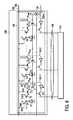
特に図1に示されるシステムにおいて検出器118として示される、本発明により使用される検出器の概略のレイアウトが、図3に示されている。検出器118は、例えばDRAMメモリ装置のような半導体メモリ装置のメモリ素子から知られているような、行及び列に沿って配置される複数のピクセル130のアレイ128を含む。アドレッシング、スイッチング及びリセットの目的で、すなわち、個別のピクセル及び/又はピクセルの個別の検出素子を個別にアドレッシングし、リセットし及び/又はスイッチングするために、半導体メモリ技術からも一般に知られているような適当なアドレッシング及び読み出し手段が設けられる。特に、図3に示される実施形態において、前記アドレッシング及び読み出し手段は、行ドライバユニット132及び列ドライバユニット134を有する。行ドライバユニット132は特に、行選択の機能を果たし、すなわち、アレイ128内の特定の行のピクセル及び/又は検出素子を個別にアドレッシングし、特定の行の中のピクセル及び/又は検出素子をリセットする。列ドライバユニット134は、特に、或る列の中のピクセルの個別の検出素子から検出信号を個別に読み出し、ピクセルの検出素子の検出信号を単一のピクセル出力信号に変換するように機能する。必要に応じて、このピクセル出力信号は、更に処理され、又は直接出力されることができる。 A schematic layout of a detector used in accordance with the present invention, shown as
特に列ドライバユニット134の一実施形態の更なる詳細が図4に示される。例示の実施形態として、ピクセル130が、16の検出素子を含み、それにより、16の検出信号が、前記検出素子から出力されるものとする。(前記特定のピクセルが、接続された行バス138を通じて適当なアドレッシング信号によってアドレスされるという条件で、)これらの検出信号は、後述される前処理の後に最終的に、16ラインの列バス136を通じて、列ドライバユニット134に出力される。列ドライバユニット134は、各列ごとに(又はより高度な実施形態では各ピクセルごとに、)信号変換回路140を有する。信号変換回路140は、(行バス138を通じて制御されるとき)現在読み出されているピクセル130のすべての検出素子からの検出信号を受け取り、ピクセル出力信号を生成する。 More details of one embodiment of the
信号変換回路140は、この例示の実施形態において、ウィナーテイクオール回路142、デジタル変換回路144及びレジスタ146を含む。ウィナーテイクオール回路142は、(この例では16の)検出信号を受け取り、同じ数の中間出力信号を出力する。詳しく後述されるように、連鎖反応により、前記中間出力信号のただ1つが、高い出力振幅をもつ信号になり、他の中間出力信号は、低い出力振幅をもつ。これらの中間出力信号は、デジタル変換回路144に供給され、デジタル変換回路144は、前記中間出力信号を、デジタル信号に変換する。例えば、16の出力信号の場合、バイナリ4ビットデジタルピクセル出力信号が生成され、その信号には、前記16の中間出力信号のうちどれが高い振幅を有したかを示す情報が符号化され、従って、情報は、ピクセル130の前記16の検出素子のうちどれが最も強い検出信号を出力したかをも示す。前記ピクセル出力信号は、それがデータ出力バス148に出力されることができるまで、記憶のためにレジスタ146に送られる。 The
列ドライバユニット134内には、デジタルデータを保持するNレジスタ146がある(N列の場合)。しかしながら、概して、一度にただ1つのレジスタ146のみを読み出すことができる。それゆえ、好適な実施形態において、どのレジスタ146を読み出すべきかを選択する付加のシフトレジスタ150が、提供される。このレジスタ150は、クロックサイクルごとに選択ポイントを1位置シフトさせるので、シフトレジスタと呼ばれる。 Within the
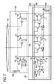
図5Aは、本発明による検出器118内の単一のピクセル130の主な回路構成の例示の実施形態を示す。例示として、前述したように単一の蛍光信号源から発するスペクトル的に異なる信号又は信号成分を受け取るために、行に沿って好適に配置された全部でn(例えば16)の検出素子をもつピクセル130について、3の検出素子D1、D2、Dnが、図示されている。それらの検出素子D1、D2、Dnは、光検出器でありうる。 FIG. 5A shows an exemplary embodiment of the main circuitry of a
更なる説明のために光検出器D1に注目して、光検出器D1は、フィールド期間中、その自己容量を放電する。N型MOSFETトランジスタT1は、リセットライン152を通るリセット信号RSによってフィールド期間ごとにパルスされるリセットスイッチである。リセットライン152は、好適には、列ドライバユニット132(図3を参照)に接続される。従って、リセットスイッチT1は、フォトダイオードD1の容量を充電し直すために、フィールド期間ごとにパルスされる。 Focusing on the photodetector D1 for further explanation, the photodetector D1 discharges its self-capacitance during the field period. The N-type MOSFET transistor T1 is a reset switch that is pulsed every field period by a reset signal RS passing through the
フォトダイオードT1のカソードの電圧V1は、電圧電流変換器として動作するP型MOSFETトランジスタT2のゲートに接続される。光検出器D1が多くの光子を受け取る場合、より多くの放電があり、従って、トランジスタT2のゲート−ソース電圧が大きくなる。従って、トランジスタTは、それが飽和領域にバイアスされるので、より多くの電流を出力する。 The cathode voltage V1 of the photodiode T1 is connected to the gate of a P-type MOSFET transistor T2 that operates as a voltage-current converter. If the photo detector D1 receives more photons, there will be more discharge and thus the gate-source voltage of the transistor T2 will increase. Thus, the transistor T outputs more current because it is biased into the saturation region.
トランジスタT2の出力電流I1は、選択スイッチとして動作するN型MOSFETトランジスタT3によって、ウィナーテイクオール回路142に供給される。前記選択スイッチT3は、選択ライン154による選択信号SSを通じてパルスされ、すなわち、選択スイッチT3は、ピクセルの当該行及び前記行のピクセル内のすべての検出素子についてフィールド期間の終わりにパルスされる。従って、前記光検出器D1乃至Dnによって生成された検出信号(すなわち電圧V1乃至Vn)から得られた電流I1乃至Inは、列バス136を通じて並行にウィナーテイクオール回路142に供給される。列バス136のバスラインは、個々のバスラインスイッチ137によってオン及びオフを別々に切り替えられることができ、バスラインスイッチ137は、バスラインアドレスバス139を通じて制御される。 The output current I1 of the transistor T2 is supplied to the winner take-all
リセットライン152及び選択ライン154が、図4に示される行アドレスバス138に対応することに注意すべきである。 Note that
図5Bには、ピクセルのこの列に関するウィナーテイクオール回路142の回路構成の実施形態が示されており、ウィナーテイクオール回路142には、前記電流I1乃至I0が、列バス136を通じて供給される。ウィナーテイクオール回路142は、この例示の実施形態において、N型MOSFETトランジスタT4、T5のnペアを含む。更には、バイアス電流IBを生成し、トランジスタT4、T5、のすべてのnペアのトランジスタT4を通じて流すためのバイアス電流源156が提供される。このバイアス電流IBは更に、トランジスタT5のゲート電圧を設定し、これは更に、トランジスタT5を流れることができる電流を固定値に設定する。 FIG. 5B shows an embodiment of the circuit configuration of the winner take-all
ウィナーテイクオール回路142の(トランジスタのnペアのうち)最も高い入力電流を有するトランジスタのペア、すなわち最も高い電流I1乃至In(すなわち最も高い輝度)が供給されるトランジスタのペアが、そのトランジスタT5に最大のドレイン電圧を生成し、当該ドレインには、関連するフォトダイオードD1からの電流I1が供給される。トランジスタT5のドレインは、トランジスタT4のゲートにも接続されている。より高いドレイン電圧が最大の入力電流によって生じることに続いて、トランジスタT4上のより高いゲート電圧が、トランジスタT4により多くの電流を流す。しかしながら、トランジスタT4を通る電流は、バイアス電流IBによって固定されているので、この追加の電流は、トランジスタT4、T5の他のペアの他のトランジスタT4を犠牲にして得られる。従って、他のペアのトランジスタT4のゲート電圧は低下し、連鎖反応はオフにされ、それによって、全バイアス電流IBは、トランジスタT4のうちわずか1つ、すなわちその対応するトランジスタT5を流れる最大電流を有する1つのトランジスタT4、を流れなければならない。それゆえ、このペアは、その中間出力線160−1に高い中間出力信号I1out(検出器素子出力信号とも呼ばれる)を供給する「ウィナー(勝者)」であり、他方、他の中間出力線160−n上の他の中間出力信号Inoutは、低い振幅を有する。The pair of transistors having the highest input current (of the n pairs of transistors) of the winner take-all
中間出力信号I1out−Inoutは、抵抗器Rによって電圧に変換され、その出力は、インバータKによってデジタルで示される。結果的に得られる信号は、並列のnラインを有することができる又は多重化バスでありうるピクセル出力バス162を通じて、ビット(デジタル)変換ユニット装置144に出力される。その中で、出力信号は、前述したようにデジタルピクセル出力信号に変換される。The intermediate output signal I1out -Inout is converted to a voltage by a resistor R, whose output is digitally indicated by an inverter K. The resulting signal is output to a bit (digital)
図6は、ピクセル130の回路構成の別の実施形態を示し、この実施形態によれば、ウィナーテイクオール回路は、図4及び図5に示される実施形態のように列ドライバユニット134の一部ではなく、ピクセル自身の一部である。ピクセルの回路構成及びウィナーテイクオール回路の概略のレイアウトは、図4及び図5に示される実施形態と同じである。勝利を得た(winning)電流は、ここでも、高い又は低い電圧を生成する抵抗器Rに供給される。抵抗器Rの後に、高く又は低く規定されるウェルを与えるインバータKが続く。この信号は、列バス136上の列を駆動する。 Figure 6 shows another embodiment of the circuit configuration of the
それゆえ、この実施形態によれば、ウィナーテイクオール回路は、列ドライバユニット134内にない。データは、ビット変換ユニット144へ直接供給される。これは、迅速なピクセル読み出しをもたらすべきであるが、ピクセルは、図4及び図5に示される実施形態と比較して、より複雑になっている。 Therefore, according to this embodiment, the winner take-all circuit is not in the
図7は、更に別の実施形態を示しており、この実施形態によれば、ピクセル130及び列ドライバ回路134は両方とも、ウィナーテイクオール回路を有し、これは、すなわち図4及び図5並びに図6に示される実施形態の混成である。しかしながら、列ドライバユニット134のウィナーテイクオール回路142'は、ここではP型であり、すなわち、N型MOSFETトランジスタT4及びT5を有するピクセル内のn型ウィナーテイクオール回路と整合するように、P型MOSFETトランジスタT4'及びT5'を有する。従って、この実施形態は、シンプルなピクセル回路を与えながらも、高速の読み出しを提供するある種のトレードオフである。ウィナーテイクオール回路142'の出力は、ビット変換ユニット144に進む。 Figure 7 shows yet another embodiment, according to this embodiment, both the
列が大きい容量を有するので、小さい電流差は、列ドライバユニット134内のウィナーテイクオール回路142'へ、直ちには送られない。従って、図5A及び図5Bに示される実施形態は、理想的な速さほどではないことがある。図6に示される実施形態において提供されるピクセル内ウィナーテイクオール回路は、大きい電流差を速くピクセルに生成する。電流差は、列全体で列ドライバユニット134内のウィナーテイクオール回路142'に送られる場合、最初は小さい電流差である。しかしながら、このウィナーテイクオール回路142'は、図5A及び図5Bに示される回路より速く判定を行うために、この少ない電流差を増幅する。 Because the column has a large capacity, a small current difference is not immediately sent to the winner take-all
本発明によれば、高いフィールドレートが得られることができ、多数のピクセルが同時に読み出し可能である。特に、複数の別個の蛍光信号源が監視されることができる。従って、本発明は、CCD技術に基づく電流検出器の制限を克服し、それらは、DNAシークエンシングシステムに適用される場合、動作スピードに関して、それらの動作限界に迅速に採用される。本発明は、別個の蛍光信号を非常に高速に監視するために、このようなDNAシークエンシングシステムに適用されることができる。例えば、単一鎖DNAの1つの分子は、1秒につき10乃至100のレートでそれらのポリメラーゼによって組み込まれる塩基を潜在的に有することができる。時間的にランダムに生じるこれらのイベントは、例えば1kHzの十分に高い読み出しレートを有する本発明の検出器によって、捕らえられることができる。各々のシークエンシング部位は、処理されるDNAの1つの分子を有し、3000部位の現在使用されている数が増大されることができる。提案されるピクセル内データ圧縮及びアナログデジタル変換は、ピクセルの数が多く(すなわち多くのシークエンシング部位をイメージングすることができる)且つ非常に高速な検出器が構築されることを可能にする。この場合、大きいアレイ上の1つのピクセルからのデジタル値の読み出しは、アナログデータよりも非常に速く実施されることができる。 According to the present invention, a high field rate can be obtained, and a large number of pixels can be read out simultaneously. In particular, a plurality of separate fluorescent signal sources can be monitored. Thus, the present invention overcomes the limitations of current detectors based on CCD technology and they are quickly adopted to their operating limits with respect to operating speed when applied to DNA sequencing systems. The present invention can be applied to such DNA sequencing systems in order to monitor separate fluorescence signals very quickly. For example, one molecule of single stranded DNA can potentially have bases incorporated by their polymerase at a rate of 10 to 100 per second. These events that occur randomly in time can be captured by the detector of the present invention having a sufficiently high readout rate of, for example, 1 kHz. Each sequencing site has one molecule of DNA to be processed, and the currently used number of 3000 sites can be increased. The proposed in-pixel data compression and analog-to-digital conversion is allows the large number of pixels (i.e., can be imaged many sequencing sites) and very fast detector is constructed. In this case, reading digital values from one pixel on a large array can be performed much faster than analog data.
本発明及びその実施形態のコンテクストにおいて、シークエンシングはDNAに制限されず、最終的な目的が核酸の塩基ペアを検出することである例えばRNA、PNA、LNAのようなシークエンシングにも関することに注意すべきである。 In the context of the present invention and its embodiments, sequencing is not limited to DNA, but the ultimate purpose is to detect nucleic acid base pairs, for example, to sequencing such as RNA, PNA, LNA. It should be noted.
本発明は、図面及び上述の説明において詳しく図示される記述されているが、このような図示及び記述は、制限的ではなく、説明的又は例示的なものであると考えられることができる。本発明は、開示される実施形態に制限されない。開示される実施形態の他の変更例は、図面、開示及び添付の請求項の検討に基づいて、請求項に記載の本発明を実施する際に当業者によって理解され実現されることができる。 While the invention has been described in detail in the drawings and foregoing description, such illustration and description are to be considered illustrative or exemplary rather than restrictive. The invention is not limited to the disclosed embodiments. Other variations of the disclosed embodiments can be understood and realized by those skilled in the art in practicing the claimed invention, based on a study of the drawings, the disclosure, and the appended claims.
請求項において、「含む、有する(comprising)」という語は、他の構成要素又はステップを除外せず、不定冠詞「a」又は「an」は、複数性を除外しない。単一の構成要素又は他のユニットが、請求項に列挙されるいくつかのアイテムの機能を果たすことができる。特定の手段が相互に異なる従属請求項に列挙されているという単なる事実は、これらの手段の組み合わせが有利に使用されることができないことを示さない。 In the claims, the word “comprising” does not exclude other elements or steps, and the indefinite article “a” or “an” does not exclude a plurality. A single component or other unit may fulfill the functions of several items recited in the claims. The mere fact that certain measures are recited in mutually different dependent claims does not indicate that a combination of these measured cannot be used to advantage.
請求項における参照符号は、本発明の範囲を制限するものとして解釈されるべきでない。 Any reference signs in the claims should not be construed as limiting the scope of the invention.
Claims (15)
Translated fromJapanese複数の別個の蛍光信号源をその上に有する基板と、
励起照明源と、
前記複数の蛍光信号源からの蛍光信号を検出する検出器と、
前記励起照明源からの励起照明を、前記基板上の前記複数の別個の蛍光信号源に同時に導くとともに、前記複数の蛍光信号源からの蛍光信号を前記検出器に導くように位置付けられる光学トレインと、
を有し、前記検出器が、
前記複数の蛍光信号源からの前記蛍光信号を個別に検出する複数のピクセルであって、各ピクセルが、受け取られた前記蛍光信号を検出し、検出信号を生成するために、予め決められた数の少なくとも2つの検出素子を有する、複数のピクセルと、
前記少なくとも2つの検出素子から前記検出信号を受け取り、前記少なくとも2つの検出素子のうちどれが最も強い検出信号を生成したかを示すピクセル出力信号を生成する信号変換回路と、
を有する装置。An apparatus for monitoring a plurality of separate fluorescent signals for DNA sequencing using fluorescently labeled nucleotides, comprising:
A substrate having a plurality of separate fluorescent signal sources thereon;
An excitation illumination source;
A detector for detecting fluorescent signals from the plurality of fluorescent signal sources;
An optical train positioned to simultaneously direct excitation illumination from the excitation illumination source to the plurality of separate fluorescence signal sources on the substrate and to direct fluorescence signals from the plurality of fluorescence signal sources to the detector; ,
And the detector is
A plurality of pixels that individually detect the fluorescence signals from the plurality of fluorescence signal sources, each pixel detecting a received fluorescence signal and generating a detection signal in a predetermined number. A plurality of pixels having at least two detection elements of
A signal conversion circuit that receives the detection signals from the at least two detection elements and generates a pixel output signal indicating which of the at least two detection elements generated the strongest detection signal;
Having a device.
ドレイン端子が、当該検出素子によって検出される検出信号を表す検出器電流信号を供給され、ソース端子が、特にグランド電位である基準電位に結合され、ゲート端子が、予め決められたバイアス電流を供給される、第1のN型MOSFETトランジスタと、
ゲート端子が、前記第1のN型MOSFETトランジスタのドレイン端子に結合され、ソース端子が、前記第1のN型MOSFETトランジスタのゲート端子に結合されて、前記予め決められたバイアス電流を供給され、ドレイン端子が、検出器素子出力信号を出力する、第2のN型MOSFETトランジスタと、
を有する、請求項9に記載の装置。The winner take-all circuit is provided for each detection element connected to the winner take-all circuit.
The drain terminal is supplied with a detector current signal representing the detection signal detected by the detection element, the source terminal is coupled to a reference potential, in particular a ground potential, and the gate terminal supplies a predetermined bias current. A first N-type MOSFET transistor,
A gate terminal is coupled to the drain terminal of the first N-type MOSFET transistor, and a source terminal is coupled to the gate terminal of the first N-type MOSFET transistor, and is supplied with the predetermined bias current; A second N-type MOSFET transistor, the drain terminal of which outputs a detector element output signal;
10. The apparatus of claim 9, comprising:
第1のウィナーテイクオール回路が、前記複数のピクセルのエリア外に配され、第2のウィナーテイクオール回路が、前記複数のピクセルのエリア内に、特に関連するピクセルのエリア内に配される、請求項9に記載の装置。For each pixel, two winner take-all circuits are associated,
A first winner take-all circuit is arranged outside the area of the plurality of pixels and a second winner take-all circuit is arranged in the area of the plurality of pixels, in particular in the area of the relevant pixels; The apparatus according to claim 9.
前記基板上の前記複数の蛍光信号源からの蛍光信号を同時に収集するために、前記基板の第1の焦点面に焦点をあわせられる対物レンズと、
前記蛍光信号のスペクトル成分を空間的に分離するスペクトル分離手段と、
前記蛍光信号の空間的に分離されたスペクトル成分を受け取り、それらを前記検出器に集束させる集束レンズと、
を有する、請求項1に記載の装置。The optical train is
An objective lens that is focused on a first focal plane of the substrate to simultaneously collect fluorescence signals from the plurality of fluorescence signal sources on the substrate;
Spectral separation means for spatially separating spectral components of the fluorescent signal;
A focusing lens that receives spatially separated spectral components of the fluorescent signal and focuses them on the detector;
The apparatus of claim 1, comprising:
前記装置が、
複数の別個の蛍光信号源をその上に有する基板と、
励起照明源と、
前記励起照明源からの励起照明を、前記基板上の前記複数の別個の蛍光信号源に同時に導き、前記複数の蛍光信号源からの蛍光信号を前記検出器に導くように位置付けられる光学トレインと、
を有し、
前記検出器が、
前記複数の蛍光信号源からの前記蛍光信号を個別に検出する複数のピクセルであって、各ピクセルが、受け取られた前記蛍光信号を検出し、検出信号を生成するために、予め決められた数の少なくとも2つの検出素子を有する、複数のピクセルと、
前記少なくとも2つの検出素子から前記検出信号を受け取り、前記少なくとも2つの検出素子のうちどれが最も強い検出信号を生成したかを示すピクセル出力信号を生成する信号変換回路と、
を有する装置。A detector for detecting fluorescent signals from a plurality of fluorescent signal sources, particularly in a device for monitoring a plurality of separate fluorescent signals for DNA sequencing using fluorescently labeled nucleotides. There,
The device is
A substrate having a plurality of separate fluorescent signal sources thereon;
An excitation illumination source;
An optical train positioned to simultaneously direct excitation illumination from the excitation illumination source to the plurality of separate fluorescence signal sources on the substrate and to direct fluorescence signals from the plurality of fluorescence signal sources to the detector;
Have
The detector is
A plurality of pixels that individually detect the fluorescence signals from the plurality of fluorescence signal sources, each pixel detecting a received fluorescence signal and generating a detection signal in a predetermined number. A plurality of pixels having at least two detection elements of
A signal conversion circuit that receives the detection signals from the at least two detection elements and generates a pixel output signal indicating which of the at least two detection elements generated the strongest detection signal;
Having a device.
Applications Claiming Priority (3)
| Application Number | Priority Date | Filing Date | Title |
|---|---|---|---|
| EP09173971.4 | 2009-10-23 | ||
| EP09173971 | 2009-10-23 | ||
| PCT/IB2010/054709WO2011048539A1 (en) | 2009-10-23 | 2010-10-18 | Device for monitoring a plurality of discrete fluorescence signals |
Publications (2)
| Publication Number | Publication Date |
|---|---|
| JP2013508718Atrue JP2013508718A (en) | 2013-03-07 |
| JP5694342B2 JP5694342B2 (en) | 2015-04-01 |
Family
ID=43500987
Family Applications (1)
| Application Number | Title | Priority Date | Filing Date |
|---|---|---|---|
| JP2012534812AActiveJP5694342B2 (en) | 2009-10-23 | 2010-10-18 | Device for monitoring multiple fluorescent signals |
Country Status (8)
| Country | Link |
|---|---|
| US (1) | US9228947B2 (en) |
| EP (1) | EP2491370B1 (en) |
| JP (1) | JP5694342B2 (en) |
| KR (1) | KR20120101396A (en) |
| CN (1) | CN102575991B (en) |
| BR (1) | BR112012009260A2 (en) |
| RU (1) | RU2543429C2 (en) |
| WO (1) | WO2011048539A1 (en) |
Cited By (2)
| Publication number | Priority date | Publication date | Assignee | Title |
|---|---|---|---|---|
| JP2015025824A (en)* | 2014-11-07 | 2015-02-05 | ソニー株式会社 | Microparticle measuring device |
| US9400251B2 (en) | 2011-09-13 | 2016-07-26 | Sony Corporation | Fine particle measuring apparatus |
Families Citing this family (3)
| Publication number | Priority date | Publication date | Assignee | Title |
|---|---|---|---|---|
| FR3048316B1 (en)* | 2016-02-29 | 2019-06-28 | Sagem Defense Securite | DEVICE FOR DETECTING A LASER SPOT |
| US20180052106A1 (en)* | 2016-08-17 | 2018-02-22 | Kerry Gunning | Dual detection scheme for dna sequencing |
| JP2018163162A (en)* | 2018-06-04 | 2018-10-18 | ソニー株式会社 | Microparticle measuring apparatus |
Citations (4)
| Publication number | Priority date | Publication date | Assignee | Title |
|---|---|---|---|---|
| JPH1123532A (en)* | 1997-07-01 | 1999-01-29 | Hitachi Electron Eng Co Ltd | Fluorescence detector |
| JP2003098006A (en)* | 2001-09-27 | 2003-04-03 | Mitsui Eng & Shipbuild Co Ltd | Electronic pulse detection device and electronic pulse detection chip |
| JP2004205335A (en)* | 2002-12-25 | 2004-07-22 | Casio Comput Co Ltd | Optical DNA sensor, DNA reader, DNA identification method, and optical DNA sensor manufacturing method |
| JP2009526997A (en)* | 2006-02-13 | 2009-07-23 | パシフィック バイオサイエンシーズ オブ カリフォルニア, インコーポレイテッド | Method and system for simultaneously monitoring optical signals from multiple sources in real time |
Family Cites Families (22)
| Publication number | Priority date | Publication date | Assignee | Title |
|---|---|---|---|---|
| US5059814A (en) | 1988-11-30 | 1991-10-22 | The California Institute Of Technology | Winner-take-all circuits for neural computing systems |
| US5561287A (en)* | 1994-09-30 | 1996-10-01 | Board Of Regents Of The University Of Colorado | Dual photodetector for determining peak intensity of pixels in an array using a winner take all photodiode intensity circuit and a lateral effect transistor pad position circuit |
| JP3176821B2 (en) | 1995-05-24 | 2001-06-18 | シャープ株式会社 | Input judgment circuit |
| US6046466A (en)* | 1997-09-12 | 2000-04-04 | Nikon Corporation | Solid-state imaging device |
| US6992709B1 (en)* | 1999-02-26 | 2006-01-31 | Intel Corporation | Method and apparatus for high-speed broadband illuminant discrimination |
| AU4061200A (en)* | 1999-03-31 | 2000-10-16 | Regents Of The University Of California, The | Multi-channel detector readout method and integrated circuit |
| US7217573B1 (en)* | 1999-10-05 | 2007-05-15 | Hitachi, Ltd. | Method of inspecting a DNA chip |
| US6362662B1 (en) | 2001-05-04 | 2002-03-26 | Winbond Electronics Corp. | Analog W.T.A. circuit reject signal |
| US6462586B1 (en)* | 2001-05-04 | 2002-10-08 | Winbond Electronics Corp. | Selectability of maximum magnitudes for K-winner take all circuit |
| US7595883B1 (en)* | 2002-09-16 | 2009-09-29 | The Board Of Trustees Of The Leland Stanford Junior University | Biological analysis arrangement and approach therefor |
| WO2004059006A1 (en)* | 2002-12-25 | 2004-07-15 | Casio Computer Co., Ltd. | Optical dna sensor, dna reading apparatus, identification method of dna and manufacturing method of optical dna sensor |
| JP4232656B2 (en)* | 2004-03-02 | 2009-03-04 | カシオ計算機株式会社 | Fluorescence detection chip |
| US7667205B2 (en)* | 2005-10-05 | 2010-02-23 | Organisation Europeenne Pour La Recherche Nucleaire | Method for determining a particle and sensor device therefor |
| US7715001B2 (en)* | 2006-02-13 | 2010-05-11 | Pacific Biosciences Of California, Inc. | Methods and systems for simultaneous real-time monitoring of optical signals from multiple sources |
| EP2021773B1 (en)* | 2006-04-19 | 2015-03-25 | IT-IS International Ltd | Reaction monitoring method and apparatus |
| JP2009540290A (en)* | 2006-06-08 | 2009-11-19 | コーニンクレッカ フィリップス エレクトロニクス エヌ ヴィ | Microelectronic sensor device for DNA detection |
| JP2008209268A (en)* | 2007-02-27 | 2008-09-11 | Casio Comput Co Ltd | Biopolymer analyzer |
| CA2687062C (en) | 2007-05-10 | 2016-04-12 | Pacific Biosciences Of California, Inc. | Methods and systems for analyzing fluorescent materials with reduced autofluorescence |
| RU2339953C1 (en)* | 2007-06-13 | 2008-11-27 | Федеральное государственное унитарное предприятие "Государственный научно-исследовательский институт биологического приборостроения" (ФГУП "ГосНИИ БП") | Method of multyanalite immunoassay with use of microparticles |
| CN100573106C (en)* | 2007-06-28 | 2009-12-23 | 大连海事大学 | A kind of optical fiber biological sensor |
| WO2009089056A1 (en) | 2008-01-10 | 2009-07-16 | Pacific Biosciences Of California, Inc. | Methods and systems for analysis of fluorescent reactions with modulated excitation |
| JP4798204B2 (en)* | 2008-10-17 | 2011-10-19 | カシオ計算機株式会社 | Fluorescence detection chip |
- 2010
- 2010-10-18USUS13/502,628patent/US9228947B2/enactiveActive
- 2010-10-18EPEP10782025.0Apatent/EP2491370B1/enactiveActive
- 2010-10-18KRKR1020127013154Apatent/KR20120101396A/ennot_activeWithdrawn
- 2010-10-18RURU2012121143/28Apatent/RU2543429C2/enactive
- 2010-10-18BRBR112012009260Apatent/BR112012009260A2/ennot_activeIP Right Cessation
- 2010-10-18JPJP2012534812Apatent/JP5694342B2/enactiveActive
- 2010-10-18WOPCT/IB2010/054709patent/WO2011048539A1/enactiveApplication Filing
- 2010-10-18CNCN201080047694.4Apatent/CN102575991B/enactiveActive
Patent Citations (4)
| Publication number | Priority date | Publication date | Assignee | Title |
|---|---|---|---|---|
| JPH1123532A (en)* | 1997-07-01 | 1999-01-29 | Hitachi Electron Eng Co Ltd | Fluorescence detector |
| JP2003098006A (en)* | 2001-09-27 | 2003-04-03 | Mitsui Eng & Shipbuild Co Ltd | Electronic pulse detection device and electronic pulse detection chip |
| JP2004205335A (en)* | 2002-12-25 | 2004-07-22 | Casio Comput Co Ltd | Optical DNA sensor, DNA reader, DNA identification method, and optical DNA sensor manufacturing method |
| JP2009526997A (en)* | 2006-02-13 | 2009-07-23 | パシフィック バイオサイエンシーズ オブ カリフォルニア, インコーポレイテッド | Method and system for simultaneously monitoring optical signals from multiple sources in real time |
Cited By (3)
| Publication number | Priority date | Publication date | Assignee | Title |
|---|---|---|---|---|
| US9400251B2 (en) | 2011-09-13 | 2016-07-26 | Sony Corporation | Fine particle measuring apparatus |
| USRE49543E1 (en) | 2011-09-13 | 2023-06-06 | Sony Corporation | Fine particle measuring apparatus |
| JP2015025824A (en)* | 2014-11-07 | 2015-02-05 | ソニー株式会社 | Microparticle measuring device |
Also Published As
| Publication number | Publication date |
|---|---|
| US9228947B2 (en) | 2016-01-05 |
| CN102575991A (en) | 2012-07-11 |
| WO2011048539A1 (en) | 2011-04-28 |
| JP5694342B2 (en) | 2015-04-01 |
| RU2012121143A (en) | 2013-11-27 |
| EP2491370A1 (en) | 2012-08-29 |
| US20120208263A1 (en) | 2012-08-16 |
| EP2491370B1 (en) | 2023-03-01 |
| KR20120101396A (en) | 2012-09-13 |
| CN102575991B (en) | 2016-06-15 |
| BR112012009260A2 (en) | 2019-09-24 |
| RU2543429C2 (en) | 2015-02-27 |
Similar Documents
| Publication | Publication Date | Title |
|---|---|---|
| US6596483B1 (en) | System and method for detecting molecules using an active pixel sensor | |
| JP3641619B2 (en) | Biological sample inspection equipment | |
| CN111926065B (en) | An efficient nucleic acid detection and gene sequencing method and device thereof | |
| JP4988023B2 (en) | Pulsed multiline excitation method for color blind fluorescence | |
| US7122799B2 (en) | LED or laser enabled real-time PCR system and spectrophotometer | |
| US20190219835A1 (en) | Super-resolution microscopy | |
| US7995202B2 (en) | Methods and systems for simultaneous real-time monitoring of optical signals from multiple sources | |
| JP5694342B2 (en) | Device for monitoring multiple fluorescent signals | |
| US7054003B2 (en) | Simultaneously reading different regions of a chemical array | |
| CN102890073A (en) | Optical detector | |
| Rasnik et al. | Electronic cameras for low‐light microscopy | |
| US20060226374A1 (en) | Method and device for identifying luminescent molecules according to the fluorescence correlation spectroscopy method | |
| EP1755167B1 (en) | Spectroscopy system for time resolved spectroscopy and its method of operation | |
| US20160115528A1 (en) | Measuring device and system for performing melting curve analysis of a dna microarray and utilization of a fluorescence detector array for analysis | |
| US20130155282A1 (en) | Image sensor readout method and apparatus | |
| JP2002350348A (en) | Fluorescence detector | |
| JP5083147B2 (en) | Biopolymer detector | |
| JP2003161699A (en) | Fluorescence detector | |
| JP2010071928A (en) | Biological macromolecule analysis support apparatus | |
| JP2010085114A (en) | Support apparatus for analysis of biopolymer |
Legal Events
| Date | Code | Title | Description |
|---|---|---|---|
| A621 | Written request for application examination | Free format text:JAPANESE INTERMEDIATE CODE: A621 Effective date:20130930 | |
| A977 | Report on retrieval | Free format text:JAPANESE INTERMEDIATE CODE: A971007 Effective date:20140326 | |
| A131 | Notification of reasons for refusal | Free format text:JAPANESE INTERMEDIATE CODE: A131 Effective date:20140529 | |
| A601 | Written request for extension of time | Free format text:JAPANESE INTERMEDIATE CODE: A601 Effective date:20140827 | |
| A602 | Written permission of extension of time | Free format text:JAPANESE INTERMEDIATE CODE: A602 Effective date:20140903 | |
| A521 | Request for written amendment filed | Free format text:JAPANESE INTERMEDIATE CODE: A523 Effective date:20141128 | |
| TRDD | Decision of grant or rejection written | ||
| A01 | Written decision to grant a patent or to grant a registration (utility model) | Free format text:JAPANESE INTERMEDIATE CODE: A01 Effective date:20150106 | |
| A61 | First payment of annual fees (during grant procedure) | Free format text:JAPANESE INTERMEDIATE CODE: A61 Effective date:20150204 | |
| R150 | Certificate of patent or registration of utility model | Ref document number:5694342 Country of ref document:JP Free format text:JAPANESE INTERMEDIATE CODE: R150 | |
| R250 | Receipt of annual fees | Free format text:JAPANESE INTERMEDIATE CODE: R250 | |
| R250 | Receipt of annual fees | Free format text:JAPANESE INTERMEDIATE CODE: R250 | |
| R250 | Receipt of annual fees | Free format text:JAPANESE INTERMEDIATE CODE: R250 | |
| R250 | Receipt of annual fees | Free format text:JAPANESE INTERMEDIATE CODE: R250 | |
| R250 | Receipt of annual fees | Free format text:JAPANESE INTERMEDIATE CODE: R250 | |
| R250 | Receipt of annual fees | Free format text:JAPANESE INTERMEDIATE CODE: R250 | |
| R250 | Receipt of annual fees | Free format text:JAPANESE INTERMEDIATE CODE: R250 | |
| R250 | Receipt of annual fees | Free format text:JAPANESE INTERMEDIATE CODE: R250 |