JP2013505549A - LIGHT EMITTING DEVICE HAVING LIGHT GUIDE PLATE HAVING REFLECTIVE Shielding Unit Accompanied With Glare - Google Patents
LIGHT EMITTING DEVICE HAVING LIGHT GUIDE PLATE HAVING REFLECTIVE Shielding Unit Accompanied With GlareDownload PDFInfo
- Publication number
- JP2013505549A JP2013505549AJP2012530379AJP2012530379AJP2013505549AJP 2013505549 AJP2013505549 AJP 2013505549AJP 2012530379 AJP2012530379 AJP 2012530379AJP 2012530379 AJP2012530379 AJP 2012530379AJP 2013505549 AJP2013505549 AJP 2013505549A
- Authority
- JP
- Japan
- Prior art keywords
- light
- guide plate
- emitting device
- light guide
- reflective
- Prior art date
- Legal status (The legal status is an assumption and is not a legal conclusion. Google has not performed a legal analysis and makes no representation as to the accuracy of the status listed.)
- Pending
Links
- 230000004313glareEffects0.000titleabstractdescription13
- 230000003287optical effectEffects0.000claimsabstractdescription59
- 239000000758substrateSubstances0.000claimsabstractdescription18
- 230000008878couplingEffects0.000claimsdescription4
- 238000010168coupling processMethods0.000claimsdescription4
- 238000005859coupling reactionMethods0.000claimsdescription4
- 239000000463materialSubstances0.000description9
- 230000004907fluxEffects0.000description4
- 238000000605extractionMethods0.000description3
- 230000009467reductionEffects0.000description3
- 239000011230binding agentSubstances0.000description2
- 238000009826distributionMethods0.000description2
- 238000005286illuminationMethods0.000description2
- 229910052751metalInorganic materials0.000description2
- 239000002184metalSubstances0.000description2
- 239000002245particleSubstances0.000description2
- 229920006254polymer filmPolymers0.000description2
- NIXOWILDQLNWCW-UHFFFAOYSA-Nacrylic acid groupChemical groupC(C=C)(=O)ONIXOWILDQLNWCW-UHFFFAOYSA-N0.000description1
- 229910052782aluminiumInorganic materials0.000description1
- XAGFODPZIPBFFR-UHFFFAOYSA-NaluminiumChemical compound[Al]XAGFODPZIPBFFR-UHFFFAOYSA-N0.000description1
- 239000003086colorantSubstances0.000description1
- 230000000694effectsEffects0.000description1
- 238000005265energy consumptionMethods0.000description1
- 238000005516engineering processMethods0.000description1
- 230000001788irregularEffects0.000description1
- 238000004519manufacturing processMethods0.000description1
- 150000002739metalsChemical class0.000description1
- 238000000034methodMethods0.000description1
- 238000012986modificationMethods0.000description1
- 230000004048modificationEffects0.000description1
- 229920000515polycarbonatePolymers0.000description1
- 239000004417polycarbonateSubstances0.000description1
- 229920000307polymer substratePolymers0.000description1
Images


Classifications
- G—PHYSICS
- G02—OPTICS
- G02B—OPTICAL ELEMENTS, SYSTEMS OR APPARATUS
- G02B6/00—Light guides; Structural details of arrangements comprising light guides and other optical elements, e.g. couplings
- G02B6/0001—Light guides; Structural details of arrangements comprising light guides and other optical elements, e.g. couplings specially adapted for lighting devices or systems
- G02B6/0011—Light guides; Structural details of arrangements comprising light guides and other optical elements, e.g. couplings specially adapted for lighting devices or systems the light guides being planar or of plate-like form
- G02B6/0013—Means for improving the coupling-in of light from the light source into the light guide
- G02B6/0015—Means for improving the coupling-in of light from the light source into the light guide provided on the surface of the light guide or in the bulk of it
- G02B6/0018—Redirecting means on the surface of the light guide
- G—PHYSICS
- G02—OPTICS
- G02B—OPTICAL ELEMENTS, SYSTEMS OR APPARATUS
- G02B6/00—Light guides; Structural details of arrangements comprising light guides and other optical elements, e.g. couplings
- G02B6/0001—Light guides; Structural details of arrangements comprising light guides and other optical elements, e.g. couplings specially adapted for lighting devices or systems
- G02B6/0011—Light guides; Structural details of arrangements comprising light guides and other optical elements, e.g. couplings specially adapted for lighting devices or systems the light guides being planar or of plate-like form
- G02B6/0033—Means for improving the coupling-out of light from the light guide
- G02B6/005—Means for improving the coupling-out of light from the light guide provided by one optical element, or plurality thereof, placed on the light output side of the light guide
- G02B6/0055—Reflecting element, sheet or layer
- G—PHYSICS
- G02—OPTICS
- G02B—OPTICAL ELEMENTS, SYSTEMS OR APPARATUS
- G02B6/00—Light guides; Structural details of arrangements comprising light guides and other optical elements, e.g. couplings
- G02B6/0001—Light guides; Structural details of arrangements comprising light guides and other optical elements, e.g. couplings specially adapted for lighting devices or systems
- G02B6/0011—Light guides; Structural details of arrangements comprising light guides and other optical elements, e.g. couplings specially adapted for lighting devices or systems the light guides being planar or of plate-like form
- G02B6/0066—Light guides; Structural details of arrangements comprising light guides and other optical elements, e.g. couplings specially adapted for lighting devices or systems the light guides being planar or of plate-like form characterised by the light source being coupled to the light guide
- G02B6/0073—Light emitting diode [LED]
- F—MECHANICAL ENGINEERING; LIGHTING; HEATING; WEAPONS; BLASTING
- F21—LIGHTING
- F21V—FUNCTIONAL FEATURES OR DETAILS OF LIGHTING DEVICES OR SYSTEMS THEREOF; STRUCTURAL COMBINATIONS OF LIGHTING DEVICES WITH OTHER ARTICLES, NOT OTHERWISE PROVIDED FOR
- F21V13/00—Producing particular characteristics or distribution of the light emitted by means of a combination of elements specified in two or more of main groups F21V1/00 - F21V11/00
- F21V13/12—Combinations of only three kinds of elements
- F—MECHANICAL ENGINEERING; LIGHTING; HEATING; WEAPONS; BLASTING
- F21—LIGHTING
- F21Y—INDEXING SCHEME ASSOCIATED WITH SUBCLASSES F21K, F21L, F21S and F21V, RELATING TO THE FORM OR THE KIND OF THE LIGHT SOURCES OR OF THE COLOUR OF THE LIGHT EMITTED
- F21Y2115/00—Light-generating elements of semiconductor light sources
- F21Y2115/10—Light-emitting diodes [LED]
- G—PHYSICS
- G02—OPTICS
- G02B—OPTICAL ELEMENTS, SYSTEMS OR APPARATUS
- G02B6/00—Light guides; Structural details of arrangements comprising light guides and other optical elements, e.g. couplings
- G02B6/0001—Light guides; Structural details of arrangements comprising light guides and other optical elements, e.g. couplings specially adapted for lighting devices or systems
- G02B6/0011—Light guides; Structural details of arrangements comprising light guides and other optical elements, e.g. couplings specially adapted for lighting devices or systems the light guides being planar or of plate-like form
- G02B6/0066—Light guides; Structural details of arrangements comprising light guides and other optical elements, e.g. couplings specially adapted for lighting devices or systems the light guides being planar or of plate-like form characterised by the light source being coupled to the light guide
- G02B6/0068—Arrangements of plural sources, e.g. multi-colour light sources
Landscapes
- Physics & Mathematics (AREA)
- General Physics & Mathematics (AREA)
- Optics & Photonics (AREA)
- Engineering & Computer Science (AREA)
- Microelectronics & Electronic Packaging (AREA)
- Planar Illumination Modules (AREA)
- Non-Portable Lighting Devices Or Systems Thereof (AREA)
- Light Guides In General And Applications Therefor (AREA)
Abstract
Translated fromJapaneseDescription
Translated fromJapanese本発明は発光装置に関し、更に詳細には内部全反射を利用した導光部を有する発光装置に関する。 The present invention relates to a light-emitting device, and more particularly to a light-emitting device having a light guide unit using total internal reflection.
ここで言及された種類の発光装置は一般に、1つ以上の発光ダイオード(LED)と、該LEDに接続して装着された導光板とから成る。これらの既知の発光装置の導光層は更に、発光面における光の脱結合のための幾つかの光学構造を有する。この種の発光装置の問題点は、LEDの使用が、例えばオフィス又はその他の作業場における照明用途に利用される場合のような幾つかの状況において、ぎらつき(glare)を引き起こす点である。例えば、欧州連合の規則は、観測者に晒される照明を、最も知覚可能な方向(垂直に対して90°乃至65°)において103cd/m2までに、他の方向において104cd/m2までに制限している。この問題を解決するための1つの試みは米国特許出願公開US2005/0265029において為されており、ここでは上述したような発光装置が開示されている。該先行技術の装置においては、各光抽出構造がそれぞれのLEDにわたって集中させられ、LED自体に近い位置において少ない光を抽出し、LEDから離れた位置において多くの光を抽出するように構成されている。これにより、ぎらつきの問題が低減される。該既知の発光装置の欠点は、種々の要件に対して既存の装置を適合させることが困難であるため、非常に限られた程度の柔軟性しか提供しない点である。変更された要件のために、より多くの光束を持つ発光装置が必要である場合には、当該先行技術による装置は、より強力なLEDによって単純に拡張され得るものではない。なぜなら、導光板が、光抽出構造による光の中の低減により或る程度のぎらつき保護を提供するように構成されているからである。従って、当該既知のシステムにおいて、より強力なLEDが利用されたとしても、ぎらつきの問題は生じてしまう。また、1つ以上のLEDが取り除かれた場合、又は1つ以上のLEDが故障した場合、対応するアレイ素子は、隣接するものよりもかなり暗くなってしまう。なぜなら、各アレイ素子は、対応するLEDに直接に晒されているからである。A light emitting device of the type mentioned here generally consists of one or more light emitting diodes (LEDs) and a light guide plate mounted in connection with the LEDs. The light guide layers of these known light emitting devices further have several optical structures for decoupling light at the light emitting surface. A problem with this type of light emitting device is that the use of LEDs causes glare in some situations, such as when used for lighting applications in offices or other workplaces, for example. For example, rules for the European Union, the exposed illumination to the observer, a most perceptible direction (90 ° to 65 ° to the vertical) by10 3 cd / m 2, 4 10 in the other direction cd / Limited to m2 . One attempt to solve this problem is made in US Patent Application Publication US2005 / 0265029, which discloses a light emitting device as described above. In the prior art device, each light extraction structure is concentrated across each LED, and is configured to extract less light at a location near the LED itself and extract more light at a location away from the LED. Yes. Thereby, the problem of glare is reduced. The disadvantage of the known light-emitting device is that it offers a very limited degree of flexibility because it is difficult to adapt existing devices to different requirements. If light emitting devices with more luminous flux are needed due to changed requirements, the prior art devices cannot simply be extended by more powerful LEDs. This is because the light guide plate is configured to provide some degree of glare protection due to the reduction in light due to the light extraction structure. Therefore, even if a more powerful LED is used in the known system, the problem of glare arises. Also, if one or more LEDs are removed, or if one or more LEDs fail, the corresponding array element will be much darker than the adjacent one. This is because each array element is directly exposed to the corresponding LED.
本発明の目的は、斯かる問題を軽減又は克服し、意図される用途に依存して、異なるタイプ及び異なる数のLEDを備えることができる発光ダイオードを提供することにある。 The object of the present invention is to reduce or overcome such problems and to provide light emitting diodes that can comprise different types and numbers of LEDs, depending on the intended application.
本発明の第1の態様によれば、本目的及び他の目的は、請求項1に記載の本発明による発光装置により達成される。従って、本発明の一態様によれば、複数の光源と導光板とを有する発光装置が提供される。前記導光板は、光出射面と、前記複数の光源に面する対向光入射面とを持つ。前記光入射面は、前記光源により発せられた光の前記導光板への結合のために配置される。前記結合された光の少なくとも一部は、内部全反射により前記導光板内を伝達され、ここで異なる光源からの光は前記導光板内で混合される。前記光出射面の少なくとも一部は、光の脱結合のための光学構造を備える。前記発光装置は更に、前記導光板に向かう前記光源の直接光の光束が前記光源の通電状態における最大密度を持つ位置において配置された反射型遮光部を有する。このようにして、光の脱結合のための各光学構造が、光源からの高密度の直接光に晒されない。その代りに、複数の光源により発せられた光の混合が、導光板へと結合し光学構造を通って脱出できる前に起こる。このことは、非常に効率的なぎらつき保護を提供する。 According to a first aspect of the present invention, this and other objects are achieved by a light emitting device according to the present invention as defined in claim 1. Therefore, according to one embodiment of the present invention, a light-emitting device including a plurality of light sources and a light guide plate is provided. The light guide plate has a light exit surface and opposing light incident surfaces facing the plurality of light sources. The light incident surface is disposed for coupling the light emitted by the light source to the light guide plate. At least a portion of the combined light is transmitted through the light guide plate by total internal reflection, where light from different light sources is mixed in the light guide plate. At least a part of the light exit surface includes an optical structure for decoupling light. The light emitting device further includes a reflection type light shielding unit disposed at a position where the light beam of the direct light of the light source toward the light guide plate has the maximum density in the energized state of the light source. In this way, each optical structure for decoupling light is not exposed to high density direct light from the light source. Instead, mixing of the light emitted by the multiple light sources occurs before it can be coupled to the light guide plate and escape through the optical structure. This provides very efficient glare protection.
該発光装置の一実施例によれば、前記反射型遮光部は、前記導光板に向かう前記光源の直接光の光束が前記光源の通電状態における最大密度を持つ位置において、前記導光板の前記光入射面に配置される。反射型遮光部は、導光板の製造の間に、導光板の光入射面に容易に配置されることができる。 According to an embodiment of the light-emitting device, the reflection-type light-shielding unit is configured such that the light of the light guide plate has a maximum density in a light-energized state of the light source toward the light guide plate. Arranged on the entrance surface. The reflective light-shielding part can be easily disposed on the light incident surface of the light guide plate during manufacture of the light guide plate.
該発光装置の一実施例によれば、前記光源は基板上に装着され、前記導光板に面する前記基板の面は前記反射型遮光部を備える。光源に向けて反射された光は、導光板に向かって反射されて戻され、それにより光学効率及び異なる光源により発せられた光の混合を向上させる。該混合はこれら光源の色温度及び光束における違いを平均化し、それにより該発光装置のビン(binning)許容度を増大させる。 According to one embodiment of the light emitting device, the light source is mounted on a substrate, and the surface of the substrate facing the light guide plate includes the reflective light shielding unit. The light reflected towards the light source is reflected back toward the light guide plate, thereby improving the optical efficiency and mixing of the light emitted by the different light sources. The mixing averages the differences in color temperature and luminous flux of these light sources, thereby increasing the binning tolerance of the light emitting device.
該発光装置の一実施例によれば、複数の光学構造が、前記導光板の前記光出射面に亘って別個の出射窓として配置され、前記導光板の前記光出射面の非構造化された領域の少なくとも一部は平坦である。光の脱結合のための光学構造及び導光板の表面にわたる平坦な部分を変更することにより、多種多様な出射窓パターンが得られるようになる。 According to one embodiment of the light emitting device, a plurality of optical structures are arranged as separate exit windows across the light exit surface of the light guide plate, and the light exit surface of the light guide plate is unstructured. At least a portion of the region is flat. By changing the optical structure for decoupling light and the flat part over the surface of the light guide plate, a wide variety of exit window patterns can be obtained.
該発光装置の一実施例によれば、光の二次脱結合を提供するために、前記導光板の平坦な光出射面の一部に粗い部分が導入される。 According to one embodiment of the light emitting device, a rough portion is introduced into a part of the flat light exit surface of the light guide plate in order to provide secondary decoupling of light.
該発光装置の一実施例によれば、前記導光板は、前記導光板の外側端に沿って配置された側壁によって前記基板に接続され、前記側壁の内面が反射型遮光部を備えられる。該反射型遮光部は、該発光装置内の光学効率及び光の混合を向上させる。 According to an embodiment of the light emitting device, the light guide plate is connected to the substrate by a side wall disposed along an outer end of the light guide plate, and an inner surface of the side wall is provided with a reflective light shielding unit. The reflective light-shielding part improves optical efficiency and light mixing in the light-emitting device.
該発光装置の一実施例によれば、前記側壁は、前記導光板の側面が露出されるように配置される。導光板の側面を露出したままとすることにより、複数の発光装置を互いに結合させ、異なる発光装置の導光板間を光が透過させられるようにすることが可能となる。 According to an embodiment of the light emitting device, the side wall is disposed such that a side surface of the light guide plate is exposed. By leaving the side surface of the light guide plate exposed, a plurality of light emitting devices can be coupled to each other so that light can be transmitted between the light guide plates of different light emitting devices.
該発光装置の一実施例によれば、前記側壁は、前記導光板の側面を被覆するように配置される。 According to an embodiment of the light emitting device, the side wall is disposed so as to cover a side surface of the light guide plate.
該発光装置の一実施例によれば、前記光源は発光ダイオードを有する。 According to one embodiment of the light emitting device, the light source comprises a light emitting diode.
該発光装置の一実施例によれば、前記光学構造は円錐形のレンズを有する。 According to one embodiment of the light emitting device, the optical structure comprises a conical lens.
該発光装置の一実施例によれば、前記光学構造は角錐形状を持つ要素を有する。 According to one embodiment of the light emitting device, the optical structure includes an element having a pyramid shape.
該発光装置の一実施例によれば、前記光学構造は拡散要素を有する。 According to one embodiment of the light emitting device, the optical structure has a diffusing element.
該発光装置の一実施例によれば、前記光学構造は反射型コリメート構造を有する。 According to one embodiment of the light emitting device, the optical structure has a reflective collimating structure.
該発光装置の一実施例によれば、前記導光板に、前記導光板の光出射面の面積の10%以上90%以下が遮光されるように反射型遮光部が備えられる。 According to one embodiment of the light emitting device, the light guide plate is provided with a reflective light shielding portion so that 10% or more and 90% or less of the area of the light emitting surface of the light guide plate is shielded.
本発明の更なる態様によれば、斯かる発光装置を有する照明器具が提供される。 According to the further aspect of this invention, the lighting fixture which has such a light-emitting device is provided.
本発明は、請求項に列挙された特徴の全てのとり得る組み合わせに関することに、留意されたい。 It should be noted that the invention relates to all possible combinations of the features recited in the claims.
本発明の本態様及びその他の態様は、本発明の実施例を示す添付図面を参照しながら、以下に詳細に説明される。 This and other aspects of the invention are described in detail below with reference to the accompanying drawings, which illustrate embodiments of the invention.
図1は、本発明の実施例による発光装置100を示す。発光装置100は、アルミニウム若しくはその他の金属又は高分子基板のような、いずれかの適切な材料でできた基板3を有する。複数の光源2(本例においてはLED)が基板3の底側に装着され、発光装置100の光出射窓の方向に下向きに光を生成するように構成される。このことは、LEDにより生成される熱が発せられる発光装置100を上向きに脱出するため、優れた熱効率をもたらす。 FIG. 1 shows a
基板3の下において基板3と略平行に、導光板4が配置される。該導光板4は、例えばアクリル又はポリカーボネートのような半透明の材料でできている。導光板4の光出射面は、光の脱結合のための1つ以上の光学構造6を備える。これら光学構造6は、該導光板の光出射面に亘って個々の光出射窓として形成されている。光学構造6は、例えば円錐形のレンズ又は角錐の形をとって備えられても良く、種々の配光を生成する(例えば同じ照明器具から同時に光と壁面照明とを生成する)ために種々のサイズ及び光抽出特性を持っていても良い。導光板4に向かう光源の直接光の光束が光源の通電状態における最大の密度を持つ位置における導光板4の光入射面において、反射型遮光部5が配置される。反射型遮光部5は例えば、金属化された層、反射性粒子を持つ結合剤、誘電性の多数積層された層、又は反射性高分子膜を含んでも良い。光源の光束が最大密度を持つ位置において導光板4が遮光されるため、反射型遮光部5は効率的なぎらつき保護をも確実にする。光源により生成された光L1、L2は3つの異なる部分に分割され、1つの部分L11、L21は光学構造6により透過され向きを変えられ、第2の部分L12、L22は反射されて光源へと戻され、第3の部分L13、L23は導光部4へと結合され、導光部4を通って伝わり、他の光源からの光と混合し、最終的に、導光板の光出射面に亘って備えられた光学構造6のいずれかを通って導光板4を脱出する。光源2に向かって反射されて戻された光L12、L22は、基板3によって、再び導光板4に向かって方向を変えられる。このことは、導光板へと結合する前であっても、異なる光源2からの光の効果的な混合をもたらす。導光板4内で生じる混合と組み合わせて、光源2が異なる明るさ及び色を持つという事実によるビン問題が効果的に低減される。また、光源2が反射型遮光部5の背後に隠蔽されるという事実により、LEDの障害が可視となり難くなり、他のものよりもかなり暗くなった1つの光学構造として現れなくなる。その代わりに、本発明による装置における個々のLEDの障害は、全ての光学構造6からの、又は或る領域内の幾つかの光学構造からの、光強度の僅かな低下として見える。反射型遮光部5は、導光板4自体に必ずしも配置される必要はない点は、留意されるべきである。導光板4に向かう光源の直接光の光束が光源の通電状態における最大の密度を持つ位置に配置される限り、光源2と導光板4の光出射面との間のいずれの位置に配置されても良い。 Under the substrate 3, the
図2乃至4を参照すると、導光板4の種々の実施例が示されている。図2においては、導光板4の光出射面の残りよりも低い位置に光学構造6が配置された、実施例200が示されている。光入射面の代わりに導光板4の光出射面に反射型遮光部7を配置することにより、光が光学構造6においてのみ導光板4から脱出することが確実にされ、同時に、導光板4の全体の厚さが一定に保たれる。 2 to 4, various embodiments of the
図3は、導光板4の光出射面の平坦な部分に、制御された粗い部分8が導入された、導光板4の実施例300を示す。当該粗い部分8は、第2の光出射面として機能し、ロゴタイプ、会社名、又は他のいずれかの所望の形状のような形状とされても良い。当該第2の光出射面は一般的に、光学構造6ほどに強い輝度は提供しないが、より輝く外観を与える。異なるパターンを生成するために、表面に亘って粗い部分8を変化させることも可能である。異なるタイプの光学構造6を用いる可能性と共に、このことは非常に大きな設計自由度をもたらす。導光板4の非構造化された表面全体に亘って斯かる制御された粗い部分を備えることも可能であり、光を逆方向に抽出することが望ましい場合には、表面の粗さは、導光板4の光入力側に備えられても良い。 FIG. 3 shows an
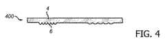
図4は、異なる配光を生成する2つの異なる光学構造6を示す。これらは単に広範なとり得る構造からの2つの例に過ぎず、図面は導光板の光出射面の異なる位置において異なるタイプの光学構造を持つことの原理を示すことを意図されている。 FIG. 4 shows two different
図5は、本発明の一実施例による発光装置600を示す。本実施例においては、導光板4に向かうLEDの直接光の光束がLEDの通電状態における最大の密度を持つ位置において、導光部4の光入射面に反射型遮光部5が配置される。当該位置において光の方向を変えるための反射型遮光部の具備は、ぎらつき問題を回避するための有効な手段である。光源として今日の高出力LEDを用いる場合には、反射型遮光部5がLED2と合わせて少なくとも60°の円錐角αを持つ円錐を形成するように、或る領域に亘って反射型遮光部5を配置することが、適切なぎらつき保護を提供するのに十分であることが分かっている。勿論、いずれかの適切な円錐角を形成するように、反射型遮光部が適合されても良い。同一の発光装置600において異なるタイプのLED2が利用される場合、反射型遮光部5は各LED2に個別に適合される。より大きな入射角については、導光板4の半透明な物質は、観測される輝度を低減させ、十分なぎらつき保護を提供する。LEDの直下の遮光部と横方向に発光する強度のための半透明な物質の漸進的なぎらつき低減特性との組み合わせは、非常に効果的なぎらつき低下概念をもたらす。ここでもまた、反射型遮光部5は、必ずしも導光板4に直接に配置される必要はない点は、留意されるべきである。導光板4に向かうLEDの直接光の光束がLEDの通電状態における最大の密度を持つ位置に配置され、且つ必要とされる円錐角が配慮される限り、光源2と導光板4の光出射面との間のいずれの位置に配置されても良い。しかしながら、効率の理由により、光源に非常に近い位置は避けられるべきである。他の可能性は、図示されていないが、基板3の一部から光の脱結合を提供することである。しばしば、例えば天井の明るさ等をつくり出すため、間接的な構成要素が望ましい。このことは、基板3において導光材料の発光島状部を備えることにより達成され得る。先に述べた導光板4と同様に、導光材料からの光の脱結合は、光学構造によって達成されるか、又は導光材料の表面に粗い部分を導入することによって達成される。 FIG. 5 shows a
更に、側壁9が、これら側壁を互いに接続する導光板4の外側端と基板3とに沿って配置される。側壁9の内面は、基板3の底面と同様に、反射型遮光部5を備えられる。ここでもまた、反射型遮光部5は例えば、金属化された層、反射性粒子を持つ結合剤、又は反射性高分子膜を含んでも良い。しかしながら、該反射型遮光部はまた、基板3及び内壁9のための適切な材料を選択することにより得られ得る。適切な材料の例には、必要ならば優れた反射特性を得るように対象となる面を処理された金属が含まれる。 Further, a side wall 9 is disposed along the outer end of the
臨界的な円錐角により定義される領域の外に配置された導光板4の光入射面における結合領域を除く、発光装置の内部に面する全ての面に反射型遮光部5を配置することは、個々のLED2により発せられる光が、更なる混合が起こる導光板4へと光が結合する前であっても、該光の非常に効果的な混合を確実にし、このことは、一般にLEDは色及び明るさの点で異なるという事実に起因するビン問題に対して該発光装置が影響を受けないようにする。例えば米国特許出願公開US2005/0265029に示されるような先行技術の方法では、各光学構造はLEDの前方に配置され、LEDにより発せられる光の殆どは外界に直接に伝達される。それ故、先行技術における個々の光学構造により発せられる光は、異なる色及び強度を持つものとして観測者に知覚される。 It is possible to dispose the reflective light-shielding
発光装置は、1つの照明器具を形成しても良い。 The light emitting device may form one luminaire.
更に図5を参照しながら、本発明の概念による発光装置による他の可能性がここで議論される。複数の発光装置600が互いに対して配置され、複数の別個の発光装置600から成る1つの照明器具を形成しても良い。必要であれば(例えばエネルギー消費上の理由又は単により弱い光が望ましい場合など)、別個の発光装置のうち1つ以上がスイッチオフされても良い。側壁9は導光板4の上端に配置され、それにより導光板4の側面を露出したままとし、導光効果により該スイッチオフされた装置の発光領域は黒くならず依然として光の輝きを発する。しかしながら、単一の発光装置600が使用されることが意図される場合には、側壁9は導光板4の側面を覆うように配置されても良い。 With further reference to FIG. 5, other possibilities with a light emitting device according to the inventive concept will now be discussed. A plurality of light emitting
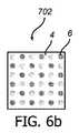
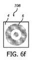
図6a乃至6fは単に、当該光学的概念により許容される多くの出射窓のうちの幾つかを提示することを意図されたものに過ぎない。灰色の領域は、光学構造6により形成される発光領域である。 FIGS. 6a to 6f are merely intended to present some of the many exit windows allowed by the optical concept. The gray area is a light emitting area formed by the
図6aは、中空の四角形の形状を持つ別の光学構造6に囲まれた正方形の光学構造を有する出射窓パターンを示す。 FIG. 6a shows an exit window pattern having a square optical structure surrounded by another
図6bは、導光板4の表面に亘って均一に分散された複数の円形の光学構造6を有する出射窓パターンを示す。 FIG. 6 b shows an exit window pattern having a plurality of circular
図6cは、6個の群に配置された複数の円形の光学構造6を有する出射窓パターンを示し、ここで各群は幾分円形のパターンを示す。 FIG. 6c shows an exit window pattern having a plurality of circular
図6dは、導光板4の表面に亘って均一に分散された複数の正方形の光学構造6を有する出射窓パターンを示す。 FIG. 6 d shows an exit window pattern having a plurality of square
図6eは、4個の群で配置された複数の円形の光学構造6を有する出射窓パターンを示し、ここで各群は傾いた正方形を示す。 FIG. 6e shows an exit window pattern having a plurality of circular
図6fは、中空の円の形を持つ別の光学構造6に囲まれた円形の光学構造を有する出射窓パターンを示す。 FIG. 6f shows an exit window pattern having a circular optical structure surrounded by another
従って、本発明による発光装置を利用すると、1つの筺体が異なる用途のための幾つかのLEDを備えることができる。また、LED技術開発は絶えずLED値毎の光束を増大させているため、継続的にシステムを適合させることが可能であることが必要である。また、本発明による発光装置におけるLEDの配置は、円錐角が配慮される限り、特に光学構造に対して幾分不規則であり、このことは低い耐性要件を持つ単純で堅固な構造を可能とする。 Thus, using the light emitting device according to the present invention, one housing can be equipped with several LEDs for different applications. In addition, since LED technology development constantly increases the luminous flux for each LED value, it is necessary to be able to adapt the system continuously. Also, the arrangement of the LEDs in the light emitting device according to the invention is somewhat irregular, especially with respect to the optical structure, as long as the cone angle is taken into account, which allows a simple and robust structure with low tolerance requirements. To do.
当業者は、本発明が以上に説明された好適な実施例に決して限定されるものではないことを理解するであろう。逆に、添付される請求項の範囲内で、多くの変更及び変形が可能である。例えば、導光板は平坦である必要はなく、曲線形状を持っても良い。更に、光源としてLEDを用いる代わりに、光源としてOLEDストリップを利用することも可能である。 Those skilled in the art will appreciate that the present invention by no means is limited to the preferred embodiments described above. On the contrary, many modifications and variations are possible within the scope of the appended claims. For example, the light guide plate does not have to be flat and may have a curved shape. Furthermore, instead of using LEDs as the light source, it is also possible to use OLED strips as the light source.
Claims (15)
Translated fromJapaneseApplications Claiming Priority (3)
| Application Number | Priority Date | Filing Date | Title |
|---|---|---|---|
| EP09170790 | 2009-09-21 | ||
| EP09170790.1 | 2009-09-21 | ||
| PCT/IB2010/054057WO2011033424A1 (en) | 2009-09-21 | 2010-09-09 | Light emitting device comprising a light guide plate with reflective shielding with glare reduction |
Publications (1)
| Publication Number | Publication Date |
|---|---|
| JP2013505549Atrue JP2013505549A (en) | 2013-02-14 |
Family
ID=43309506
Family Applications (1)
| Application Number | Title | Priority Date | Filing Date |
|---|---|---|---|
| JP2012530379APendingJP2013505549A (en) | 2009-09-21 | 2010-09-09 | LIGHT EMITTING DEVICE HAVING LIGHT GUIDE PLATE HAVING REFLECTIVE Shielding Unit Accompanied With Glare |
Country Status (5)
| Country | Link |
|---|---|
| US (1) | US8721101B2 (en) |
| EP (1) | EP2480918B8 (en) |
| JP (1) | JP2013505549A (en) |
| CN (1) | CN102511012B (en) |
| WO (1) | WO2011033424A1 (en) |
Cited By (3)
| Publication number | Priority date | Publication date | Assignee | Title |
|---|---|---|---|---|
| JP2015022799A (en)* | 2013-07-16 | 2015-02-02 | 東洋電装株式会社 | Switch device |
| KR20160044677A (en)* | 2014-10-15 | 2016-04-26 | 삼성디스플레이 주식회사 | Backlight unit and display device having the same |
| JP2019511840A (en)* | 2016-03-16 | 2019-04-25 | ルミレッズ ホールディング ベーフェー | Method of manufacturing LED module |
Families Citing this family (22)
| Publication number | Priority date | Publication date | Assignee | Title |
|---|---|---|---|---|
| EP3133579B1 (en) | 2010-01-29 | 2020-03-04 | Avery Dennison Corporation | Smart sign box using electronic interactions |
| US10977965B2 (en) | 2010-01-29 | 2021-04-13 | Avery Dennison Retail Information Services, Llc | Smart sign box using electronic interactions |
| KR101830718B1 (en)* | 2011-07-15 | 2018-02-22 | 엘지이노텍 주식회사 | display apparatus |
| CN104025556B (en) | 2011-09-01 | 2018-08-10 | 艾利丹尼森公司 | Equipment, system and method for consumer's tracking |
| US8630908B2 (en) | 2011-11-02 | 2014-01-14 | Avery Dennison Corporation | Distributed point of sale, electronic article surveillance, and product information system, apparatus and method |
| EP2828573B1 (en)* | 2012-03-18 | 2017-05-10 | Robe Lighting, Inc | Improved collimation system for an led luminaire |
| US8934173B2 (en) | 2012-08-21 | 2015-01-13 | Svv Technology Innovations, Inc. | Optical article for illuminating building interiors with sunlight |
| US9734365B2 (en) | 2012-09-10 | 2017-08-15 | Avery Dennison Retail Information Services, Llc | Method for preventing unauthorized diversion of NFC tags |
| BR112014017152B8 (en) | 2012-10-18 | 2022-08-30 | Avery Dennison Corp | METHOD AND SYSTEM FOR NFC SECURITY |
| JP6250687B2 (en) | 2012-10-26 | 2017-12-20 | フィリップス ライティング ホールディング ビー ヴィ | Lighting device and lighting system |
| US9767329B2 (en) | 2012-11-19 | 2017-09-19 | Avery Dennison Retail Information Services, Llc | NFC tags with proximity detection |
| US9655191B2 (en)* | 2013-01-25 | 2017-05-16 | Philips Lighting Holding B.V. | Lighting device and lighting system |
| DE102013106689B4 (en)* | 2013-06-26 | 2022-02-03 | OSRAM Opto Semiconductors Gesellschaft mit beschränkter Haftung | Optoelectronic semiconductor component |
| AT515640A1 (en)* | 2014-03-31 | 2015-10-15 | Werner Färber | lighting device |
| JP6367608B2 (en)* | 2014-05-19 | 2018-08-01 | 矢崎総業株式会社 | Vehicle display device |
| AT16410U1 (en)* | 2015-10-09 | 2019-08-15 | Zumtobel Lighting Gmbh | Arrangement for surface light emission |
| EP3446030B1 (en)* | 2016-04-22 | 2019-12-18 | Signify Holding B.V. | Pebble-plate like louvre |
| US10649130B2 (en) | 2016-04-22 | 2020-05-12 | Signify Holding B.V. | Pebble-plate like louvre with specific domain characteristics |
| JP6796746B1 (en)* | 2019-02-21 | 2020-12-09 | ミネベアミツミ株式会社 | Planar lighting device |
| FR3105357B1 (en)* | 2019-12-19 | 2022-01-07 | Gilbert Paulezec | Luminous cover panel and assembly comprising it |
| US11835213B2 (en)* | 2021-08-19 | 2023-12-05 | Matthew Hartley | Lighting fixtures with improved lighting components |
| TWI827475B (en)* | 2023-02-23 | 2023-12-21 | 群光電子股份有限公司 | Electronic device with light emitting function |
Citations (6)
| Publication number | Priority date | Publication date | Assignee | Title |
|---|---|---|---|---|
| JP2002324409A (en)* | 2001-01-20 | 2002-11-08 | Koninkl Philips Electronics Nv | Colored lighting system |
| EP1640756A1 (en)* | 2004-09-27 | 2006-03-29 | Barco N.V. | Methods and systems for illuminating |
| JP2006310045A (en)* | 2005-04-27 | 2006-11-09 | Sony Corp | Backlight device and display device |
| JP2006344409A (en)* | 2005-06-07 | 2006-12-21 | Seiko Instruments Inc | Light fixture, and display device provided with the same |
| JP2007227286A (en)* | 2006-02-27 | 2007-09-06 | Seiko Instruments Inc | Lighting device and display device using the same |
| WO2009068007A1 (en)* | 2007-11-30 | 2009-06-04 | Osram Opto Semiconductors Gmbh | Illumination device |
Family Cites Families (23)
| Publication number | Priority date | Publication date | Assignee | Title |
|---|---|---|---|---|
| US5386347A (en) | 1992-10-02 | 1995-01-31 | Photo Craft Co., Ltd. | Illuminating apparatus and a method of manufacturing an edge light conductor for use therein |
| US6301002B1 (en)* | 1993-12-22 | 2001-10-09 | Eastman Kodak Company | Film holder |
| JP3521058B2 (en) | 1998-06-12 | 2004-04-19 | 株式会社エンプラス | Light guide plate, side light type surface light source device and liquid crystal display device |
| WO2000050808A1 (en) | 1999-02-24 | 2000-08-31 | 3M Innovative Properties Company | Illumination device for producing predetermined intensity patterns |
| DE10102586A1 (en)* | 2001-01-20 | 2002-07-25 | Philips Corp Intellectual Pty | Luminair with light emission surface and punctiform light sources |
| JP4397728B2 (en)* | 2004-04-21 | 2010-01-13 | 日東電工株式会社 | Direct type backlight |
| US7997771B2 (en) | 2004-06-01 | 2011-08-16 | 3M Innovative Properties Company | LED array systems |
| KR20060012959A (en)* | 2004-08-05 | 2006-02-09 | 삼성전자주식회사 | Backlight for display device |
| TWI249257B (en)* | 2004-09-24 | 2006-02-11 | Epistar Corp | Illumination apparatus |
| KR101189080B1 (en) | 2005-01-24 | 2012-11-09 | 삼성디스플레이 주식회사 | Reflecting plate and liquid crystal display device having the same |
| KR101174770B1 (en) | 2005-02-28 | 2012-08-17 | 엘지디스플레이 주식회사 | back light unit and liquid crystal display device using the same |
| EP1933080A4 (en)* | 2005-09-15 | 2008-10-29 | Zeon Corp | Directly downward type backlight device |
| JP4280283B2 (en) | 2006-01-27 | 2009-06-17 | 株式会社オプトデザイン | Surface illumination light source device and surface illumination device using the same |
| CN101126822B (en)* | 2006-08-18 | 2010-09-29 | 鸿富锦精密工业(深圳)有限公司 | Optical board and backlight module using the optical board |
| JP5420415B2 (en) | 2006-10-16 | 2014-02-19 | コーニンクレッカ フィリップス エヌ ヴェ | Flat thin LED lighting device |
| US20080089093A1 (en)* | 2006-10-17 | 2008-04-17 | Miller Anne M | Backlight unit using particular direct backlight assembly |
| JP2010511268A (en) | 2006-11-28 | 2010-04-08 | コーニンクレッカ フィリップス エレクトロニクス エヌ ヴィ | Light guiding layer with integrated mixing and light extraction area |
| TW200825529A (en)* | 2006-12-06 | 2008-06-16 | Chi Lin Technology Co Ltd | Light mixer and backlight module having it |
| CN101308225B (en)* | 2007-05-18 | 2011-07-27 | 鸿富锦精密工业(深圳)有限公司 | Backlight module group and its optical plate |
| US20090086508A1 (en)* | 2007-09-27 | 2009-04-02 | Philips Lumileds Lighting Company, Llc | Thin Backlight Using Low Profile Side Emitting LEDs |
| US7791683B2 (en)* | 2007-11-19 | 2010-09-07 | Honeywell International Inc. | Backlight systems for liquid crystal displays |
| GB2448564B (en)* | 2007-11-26 | 2009-04-29 | Iti Scotland Ltd | Light guides |
| JP2009283438A (en)* | 2007-12-07 | 2009-12-03 | Sony Corp | Lighting device, display device, and manufacturing method of lighting device |
- 2010
- 2010-09-09USUS13/496,937patent/US8721101B2/ennot_activeExpired - Fee Related
- 2010-09-09WOPCT/IB2010/054057patent/WO2011033424A1/enactiveApplication Filing
- 2010-09-09CNCN201080042017.3Apatent/CN102511012B/ennot_activeExpired - Fee Related
- 2010-09-09JPJP2012530379Apatent/JP2013505549A/enactivePending
- 2010-09-09EPEP10763016.2Apatent/EP2480918B8/ennot_activeNot-in-force
Patent Citations (6)
| Publication number | Priority date | Publication date | Assignee | Title |
|---|---|---|---|---|
| JP2002324409A (en)* | 2001-01-20 | 2002-11-08 | Koninkl Philips Electronics Nv | Colored lighting system |
| EP1640756A1 (en)* | 2004-09-27 | 2006-03-29 | Barco N.V. | Methods and systems for illuminating |
| JP2006310045A (en)* | 2005-04-27 | 2006-11-09 | Sony Corp | Backlight device and display device |
| JP2006344409A (en)* | 2005-06-07 | 2006-12-21 | Seiko Instruments Inc | Light fixture, and display device provided with the same |
| JP2007227286A (en)* | 2006-02-27 | 2007-09-06 | Seiko Instruments Inc | Lighting device and display device using the same |
| WO2009068007A1 (en)* | 2007-11-30 | 2009-06-04 | Osram Opto Semiconductors Gmbh | Illumination device |
Cited By (4)
| Publication number | Priority date | Publication date | Assignee | Title |
|---|---|---|---|---|
| JP2015022799A (en)* | 2013-07-16 | 2015-02-02 | 東洋電装株式会社 | Switch device |
| KR20160044677A (en)* | 2014-10-15 | 2016-04-26 | 삼성디스플레이 주식회사 | Backlight unit and display device having the same |
| KR102278308B1 (en)* | 2014-10-15 | 2021-07-19 | 삼성디스플레이 주식회사 | Backlight unit and display device having the same |
| JP2019511840A (en)* | 2016-03-16 | 2019-04-25 | ルミレッズ ホールディング ベーフェー | Method of manufacturing LED module |
Also Published As
| Publication number | Publication date |
|---|---|
| EP2480918B8 (en) | 2016-09-21 |
| US8721101B2 (en) | 2014-05-13 |
| WO2011033424A1 (en) | 2011-03-24 |
| EP2480918B1 (en) | 2016-07-20 |
| CN102511012B (en) | 2014-10-15 |
| CN102511012A (en) | 2012-06-20 |
| US20120176813A1 (en) | 2012-07-12 |
| EP2480918A1 (en) | 2012-08-01 |
Similar Documents
| Publication | Publication Date | Title |
|---|---|---|
| JP2013505549A (en) | LIGHT EMITTING DEVICE HAVING LIGHT GUIDE PLATE HAVING REFLECTIVE Shielding Unit Accompanied With Glare | |
| US10215911B2 (en) | Lighting assembly | |
| JP5658752B2 (en) | Freeform light module | |
| EP2478397B1 (en) | Light-emitting device | |
| RU2639980C2 (en) | Lighting device with circular distribution of light | |
| US20130027927A1 (en) | Floating light luminaire | |
| US9605830B1 (en) | Systems, methods and devices for an LED lighting module with a light transmissive cover | |
| KR20120042845A (en) | LED-based lamps and light emitting signage | |
| JP2006525684A5 (en) | ||
| CA2826903C (en) | Blade of light luminaire | |
| JP2009516892A (en) | Lighting device | |
| TW201202624A (en) | Edge-light type lighting device | |
| RU2633924C2 (en) | Lighting device on basis of heat-conductive sheet with light-diffusing particles | |
| JP2011216482A (en) | Lighting system and light guide plate | |
| JP3211553U (en) | Lighting device | |
| CN101498427B (en) | Uniform light emitting device | |
| JP3156238U (en) | Curved light guide illuminator | |
| JP2012243680A (en) | Lighting system | |
| JP5449098B2 (en) | Lighting device | |
| JP6204722B2 (en) | lighting equipment | |
| RU2706799C1 (en) | Flat led illuminator with wide range of light power and internal illumination | |
| CN110319375A (en) | Lighting device | |
| KR102795369B1 (en) | Lighting apparatus | |
| JP7122539B2 (en) | lighting equipment | |
| KR101341419B1 (en) | Light guide plate for enhanced light efficiency and led illuminating device having thereof |
Legal Events
| Date | Code | Title | Description |
|---|---|---|---|
| A621 | Written request for application examination | Free format text:JAPANESE INTERMEDIATE CODE: A621 Effective date:20130906 | |
| A131 | Notification of reasons for refusal | Free format text:JAPANESE INTERMEDIATE CODE: A131 Effective date:20140507 | |
| A521 | Request for written amendment filed | Free format text:JAPANESE INTERMEDIATE CODE: A523 Effective date:20140805 | |
| A02 | Decision of refusal | Free format text:JAPANESE INTERMEDIATE CODE: A02 Effective date:20150106 | |
| A521 | Request for written amendment filed | Free format text:JAPANESE INTERMEDIATE CODE: A523 Effective date:20150424 | |
| A911 | Transfer to examiner for re-examination before appeal (zenchi) | Free format text:JAPANESE INTERMEDIATE CODE: A911 Effective date:20150501 | |
| A912 | Re-examination (zenchi) completed and case transferred to appeal board | Free format text:JAPANESE INTERMEDIATE CODE: A912 Effective date:20150703 | |
| RD02 | Notification of acceptance of power of attorney | Free format text:JAPANESE INTERMEDIATE CODE: A7422 Effective date:20151005 | |
| A711 | Notification of change in applicant | Free format text:JAPANESE INTERMEDIATE CODE: A711 Effective date:20160330 | |
| RD02 | Notification of acceptance of power of attorney | Free format text:JAPANESE INTERMEDIATE CODE: A7422 Effective date:20160408 | |
| RD04 | Notification of resignation of power of attorney | Free format text:JAPANESE INTERMEDIATE CODE: A7424 Effective date:20160418 |