JP2013254814A - Semiconductor device manufacturing process and semiconductor device manufactured thereby - Google Patents
Semiconductor device manufacturing process and semiconductor device manufactured therebyDownload PDFInfo
- Publication number
- JP2013254814A JP2013254814AJP2012128744AJP2012128744AJP2013254814AJP 2013254814 AJP2013254814 AJP 2013254814AJP 2012128744 AJP2012128744 AJP 2012128744AJP 2012128744 AJP2012128744 AJP 2012128744AJP 2013254814 AJP2013254814 AJP 2013254814A
- Authority
- JP
- Japan
- Prior art keywords
- substrate
- semiconductor layer
- semiconductor device
- layer
- manufacturing process
- Prior art date
- Legal status (The legal status is an assumption and is not a legal conclusion. Google has not performed a legal analysis and makes no representation as to the accuracy of the status listed.)
- Pending
Links
Images


Landscapes
- Led Device Packages (AREA)
- Led Devices (AREA)
Abstract
Translated fromJapaneseDescription
Translated fromJapanese本発明は半導体デバイス製造工程及びその製造工程を経て製造された半導体デバイスに関する。 The present invention relates to a semiconductor device manufacturing process and a semiconductor device manufactured through the manufacturing process.
半導体は今や日常生活に欠かせない存在である。照明の分野でも半導体デバイスの一種である発光ダイオード(LED)が従来の蛍光灯や白熱灯にとって代わりつつある。またLEDがテレビジョン、パーソナルコンピュータ、携帯電話などの液晶表示パネルのバックライトや、交通信号機などに用いられていることは多くの人の知るところである。 Semiconductors are indispensable for everyday life. In the field of lighting, light emitting diodes (LEDs), which are a type of semiconductor device, are replacing conventional fluorescent lamps and incandescent lamps. In addition, many people know that LEDs are used in backlights of liquid crystal display panels such as televisions, personal computers, mobile phones, and traffic signals.
LEDとして用いられる半導体には様々な種類のものがあるが、最近ではGaN、AlN、InN及びそれらの混晶に代表される窒化物半導体が注目されている。窒化物半導体はAlGaInAs系半導体やAlGaInP系半導体に比べてバンドギャップEgが大きく、直接遷移型であるため、紫外線から緑色に及ぶ波長領域での発光が可能である。窒化物半導体はこのような特質を生かして、各種波長の光を出力する半導体レーザ素子や、紫外線から赤色光までの広い発光波長範囲をカバーできるLEDなどに用いることができる。 There are various types of semiconductors used as LEDs. Recently, nitride semiconductors represented by GaN, AlN, InN, and mixed crystals thereof have attracted attention. Nitride semiconductors have a larger band gap Eg than AlGaInAs-based semiconductors and AlGaInP-based semiconductors, and are direct transition types, and thus can emit light in a wavelength region ranging from ultraviolet to green. Nitride semiconductors can be used for semiconductor laser elements that output light of various wavelengths, LEDs that can cover a wide emission wavelength range from ultraviolet light to red light, and the like by taking advantage of such characteristics.
発光波長範囲が広い窒化物半導体は、プロジェクターやフルカラーディスプレイへの応用が考えられている。また、発光波長を短波長化できるという特質を生かして、殺菌・浄水・公害物質の高速分解といった公衆衛生・環境分野への適用や、各種医療分野への適用に期待が高まっている。それに伴い、深紫外領域(波長:200nm〜350nm)で発光するデバイスの研究開発が各研究機関で精力的に進められている。 Nitride semiconductors with a wide emission wavelength range are considered for application to projectors and full-color displays. In addition, taking advantage of the characteristic that the emission wavelength can be shortened, there is an increasing expectation for application to public health / environment fields such as sterilization, water purification, high-speed decomposition of pollutants, and various medical fields. Along with this, research and development of devices that emit light in the deep ultraviolet region (wavelength: 200 nm to 350 nm) are being energetically promoted by each research institution.
窒化物半導体を用いた発光デバイスの構造例を図42に示す。発光デバイス100は、サファイアなどからなる基板101の上に図のような形状の窒化物半導体層102を成長させ、窒化物半導体層102の一箇所にn電極103を形成し、他の箇所にp電極104を形成したものである。n電極103とp電極104はAuを含む合金からなる。 An example of the structure of a light emitting device using a nitride semiconductor is shown in FIG. In the
図42の構造の発光デバイス100には次のような問題があった。Alの組成比が高いn−AlGaN層106にあっては、電子の到達しやすい領域105aに電流が集中し、その領域105aで電子とホールの結合が集中的に生じることになる。すなわち発光箇所が限定され、大面積発光を得ることが困難となる。 The
上記の問題は、発光デバイス100が殺菌用途で用いられる短波長光(例えば波長250nm〜280nm程度)を発するものである場合、一層顕著に現れる。このような用途の発光デバイスでは、活性層量子井戸のAl組成や、p型窒化物半導体層、n型窒化物半導体層のAl組成などが50%を超えることもあり、電流の広がりがさらに悪くなるからである。 The above problem appears more prominently when the
図42の構造の発光デバイス100の問題点を解決するため、図43に示す構造の発光デバイス110が提案されている。発光デバイス110は、基板111の上に窒化物半導体層112を成長させた後、窒化物半導体層112から基板111を分離し、窒化物半導体層112をn電極113とp電極114で挟んだものである。このように半導体を形成する母体となる基板を半導体層から分離し、残された半導体層を電極で挟んだ構造は「縦型構造」と呼ばれる。これに対して図42に示す構造は「横型構造」と呼ばれる。 In order to solve the problem of the
横型構造の半導体デバイスではn型半導体層(例えばGaNやAlGaN)を流れる電流の経路長が数十μmに達するのに対し、縦型構造の半導体デバイスではn型半導体層を流れる電流の経路長を数μm以下へと大幅に削減できる。電流の経路長が短くなれば抵抗が低減し、電流が均一に流れるようになる。このため縦型半導体デバイスを用いたLEDでは発光領域がLED全体に拡大する。このように、半導体デバイスを縦型構造にすることは、LEDの大出力化にあたり有力な手段と考えられている。また、動作電圧を低減できるため、LED素子の発熱が抑制され、発熱による発光効率の低下や信頼性の劣化を抑制する事が可能となる。 In the semiconductor device with the horizontal structure, the path length of the current flowing through the n-type semiconductor layer (for example, GaN or AlGaN) reaches several tens of μm, whereas in the semiconductor device with the vertical structure, the path length of the current flowing through the n-type semiconductor layer is increased. It can be greatly reduced to several μm or less. When the current path length is shortened, the resistance is reduced and the current flows uniformly. For this reason, in the LED using the vertical semiconductor device, the light emitting region extends to the entire LED. Thus, it is considered that making the semiconductor device a vertical structure is an effective means for increasing the output of the LED. Further, since the operating voltage can be reduced, heat generation of the LED element is suppressed, and it is possible to suppress a decrease in light emission efficiency and a deterioration in reliability due to the heat generation.
縦型構造の半導体デバイスを形成するためには、基板上に半導体層を成長させた後、半導体層から基板を分離する必要がある。このような目的で半導体層から基板を分離する方法の一例を特許文献1に見ることができる。特許文献1記載の方法では、半導体層と基板の界面にレーザービームを照射して界面を分離させ、基板を分離する。この方法はレーザーリフトオフ法と呼ばれている。 In order to form a semiconductor device having a vertical structure, it is necessary to grow a semiconductor layer on the substrate and then to separate the substrate from the semiconductor layer. An example of a method for separating a substrate from a semiconductor layer for such a purpose can be seen in
窒化物半導体で縦型構造の半導体デバイスを形成する場合、窒化物半導体層の層厚は通常数十μm以下であるため、基板を分離してしまうと極薄膜の窒化物半導体層がとり残されることになる。このような極薄膜の窒化物半導体層は取り扱いが困難なので、窒化物半導体層の成長に用いた基板とは別の存在である支持基板に予め窒化物半導体層を貼り付けておき、その後に基板を分離するという手順がとられる。 When forming a semiconductor device having a vertical structure with a nitride semiconductor, the layer thickness of the nitride semiconductor layer is usually several tens of μm or less. Therefore, if the substrate is separated, an ultrathin nitride semiconductor layer is left behind. It will be. Since such an ultra-thin nitride semiconductor layer is difficult to handle, a nitride semiconductor layer is attached in advance to a support substrate that is different from the substrate used for the growth of the nitride semiconductor layer, and then the substrate The procedure of separating is taken.
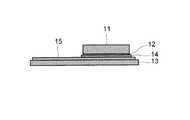
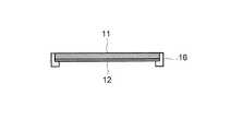
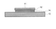
支持基板に窒化物半導体層を貼り付けるにあたっては、はんだや熱可塑性樹脂などの貼り付け材料層を支持基板上に形成しておき、その貼り付け材料層に加熱圧着で窒化物半導体層を貼り付けるという方法が用いられる。支持基板に窒化物半導体層を貼り付けた後の状態が図44及び図45に示されている。図44及び図45において、11は基板、12は窒化物半導体層、13は支持基板、14は貼り付け材料層である。 When attaching the nitride semiconductor layer to the support substrate, an adhesive material layer such as solder or thermoplastic resin is formed on the support substrate, and the nitride semiconductor layer is attached to the adhesive material layer by thermocompression bonding. The method is used. 44 and 45 show a state after the nitride semiconductor layer is attached to the support substrate. 44 and 45, 11 is a substrate, 12 is a nitride semiconductor layer, 13 is a support substrate, and 14 is a bonding material layer.
加熱圧着工程で窒化物半導体層12を貼り付け材料層14に押し付けると、貼り付け材料層14が拡がって窒化物半導体層12の外側に不均一にはみ出すことがある。図46及び図47に示す例のように、基板11及び窒化物半導体層12よりも広い面積に貼り付け材料層14が形成されていた場合、窒化物半導体層12が貼り付け材料層14の中に沈み込む形になり、窒化物半導体層12の側面に貼り付け材料層14が付着する。 When the
貼り付け材料層14の付着が窒化物半導体層12の側面だけで済めばよい。しかしながら、前述の通り窒化物半導体層12は層厚が数十μm以下という極薄膜であるため、貼り付け材料層14の方が窒化物半導体層12よりも厚くなっているのが普通である。その結果、窒化物半導体層12は貼り付け材料層14の中に完全に埋め込まれ、貼り付け材料層14が基板11の側面にも付着することになる。貼り付け材料層14が基板11の側面に付着すると基板11が支持基板13に接着された形になり、後工程で基板11を窒化物半導体層12から分離しようとしても、基板11を分離できないという事態が生じ得る。 The attachment of the
上記の問題を回避する方策の一つは、加熱圧着工程を経ても貼り付け材料層14が窒化物半導体層12の外側にはみ出さないように、貼り付け材料層14の塗布面積を小さくしておく、というものである。そのようにした構成例を図48及び図49に示す。このようにすれば、窒化物半導体層12の側面にも基板11の側面にも貼り付け材料層14が付着することはないが、貼り付け材料層14によって接着されていない部分が窒化物半導体層12の端に不均一、不定形な形で生じるため、窒化物半導体層12の発光面積が素子毎に不均一になる。このため、出力基準値を満たさない半導体デバイスの割合が多くなり、製造の歩留まりが悪化するという新たな問題が生じる。 One measure for avoiding the above problem is to reduce the application area of the
本発明は上記の点に鑑みなされたものであり、基板とその上に形成された半導体層の界面に電磁放射線を照射して基板と半導体層を界面で分離する工程の前処理として、半導体層を基板とは別の支持基板に貼り付けるにあたり、貼り付け材料層が基板の側面に付着して基板の分離が妨げられるという事態が生じるのを防ぐことを目的とする。 The present invention has been made in view of the above points, and as a pretreatment of the step of irradiating the interface between the substrate and the semiconductor layer formed thereon with electromagnetic radiation to separate the substrate and the semiconductor layer at the interface, the semiconductor layer It is an object of the present invention to prevent the occurrence of a situation in which the attachment material layer adheres to the side surface of the substrate and the separation of the substrate is prevented when the substrate is attached to a support substrate different from the substrate.
上記目的を達成するため、本発明に係る半導体デバイス製造工程は、基板とその上に形成された半導体層の界面に電磁放射線を照射して前記基板と前記半導体層を分離する工程の前処理として、前記半導体層を前記基板とは別の支持基板に貼り付けるにあたり、前記基板と前記半導体層の側面に保護膜を形成する工程と、前記保護膜が形成された前記半導体層を貼り付け材料層を介して、前記支持基板に貼り付ける工程と、前記貼り付け材料層を介して、前記支持基板に貼り付けられた前記半導体層、及び前記基板から、前記保護膜を除去する工程と、が遂行されることを特徴としている。 In order to achieve the above object, a semiconductor device manufacturing process according to the present invention is a pretreatment of a process of separating the substrate and the semiconductor layer by irradiating electromagnetic radiation to the interface between the substrate and the semiconductor layer formed thereon. In attaching the semiconductor layer to a support substrate different from the substrate, a step of forming a protective film on the side surface of the substrate and the semiconductor layer, and a material layer for attaching the semiconductor layer on which the protective film is formed The step of attaching to the support substrate via the step, and the step of removing the protective film from the semiconductor layer attached to the support substrate and the substrate via the attachment material layer are performed. It is characterized by being.
上記半導体デバイス製造工程において、前記半導体層を前記基板とは別の支持基板に貼り付けるにあたり、前記半導体層よりも厚さが大である前記貼り付け材料層を介して、貼り付けることが好ましい。 In the semiconductor device manufacturing process, when the semiconductor layer is attached to a support substrate different from the substrate, the semiconductor layer is preferably attached via the attachment material layer having a thickness larger than that of the semiconductor layer.
上記半導体デバイス製造工程において、前記基板と前記半導体層は、前記保護膜形成前に1チップの大きさに分割されることが好ましい。 In the semiconductor device manufacturing process, it is preferable that the substrate and the semiconductor layer are divided into a size of one chip before forming the protective film.
上記半導体デバイス製造工程において、前記支持基板は、前記1チップの大きさに分割された前記基板と前記半導体層を貼り付けるのに適した大きさにされることが好ましい。 In the semiconductor device manufacturing process, it is preferable that the support substrate has a size suitable for attaching the substrate divided into the size of the one chip and the semiconductor layer.
上記半導体デバイス製造工程において、前記半導体層の一部が発光デバイスの発光部となることが好ましい。 In the semiconductor device manufacturing process, a part of the semiconductor layer is preferably a light emitting part of the light emitting device.
上記半導体デバイス製造工程において、前記半導体層は、前記基板に接する面よりもその反対側の面の方が面積小となるように側面が傾斜した形にされることが好ましい。 In the semiconductor device manufacturing process, it is preferable that the semiconductor layer has a side surface inclined such that the surface opposite to the surface in contact with the substrate has a smaller area.
上記半導体デバイス製造工程において、前記基板は、前記半導体層に接する面よりもその反対側の面の方が面積大となるように側面が傾斜した形にされることが好ましい。 In the semiconductor device manufacturing process, it is preferable that the substrate has a side surface inclined such that the surface opposite to the surface in contact with the semiconductor layer has a larger area.
上記半導体デバイス製造工程において、前記保護膜を除去した後に前記半導体層の側面に対峙する前記貼り付け材料層の面が、前記半導体層の側面から出射した光を前記保護膜除去後の空間の外側へと反射する傾斜面となるように、前記保護膜は側面が傾斜した形にされることが好ましい。 In the semiconductor device manufacturing step, the surface of the bonding material layer facing the side surface of the semiconductor layer after the removal of the protective film causes light emitted from the side surface of the semiconductor layer to be outside the space after the removal of the protective film. It is preferable that the protective film has an inclined side surface so as to form an inclined surface that reflects toward the surface.
上記半導体デバイス製造工程において、前記貼り付け材料層は、前記保護膜除去後に前記半導体層の側面に対峙する面の光反射率が高められていることが好ましい。 In the semiconductor device manufacturing process, it is preferable that the adhesive material layer has an increased light reflectance on a surface facing the side surface of the semiconductor layer after the protective film is removed.
上記半導体デバイス製造工程において、前記貼り付け材料層に光反射率の高い材料が用いられていることが好ましい。 In the semiconductor device manufacturing process, it is preferable that a material having high light reflectance is used for the attachment material layer.
上記半導体デバイス製造工程において、前記基板は、研磨して薄くする工程を経たものであることが好ましい。 In the semiconductor device manufacturing process, the substrate is preferably subjected to a process of polishing and thinning.
上記半導体デバイス製造工程において、半導体デバイスのチップ形状が角形であることが好ましい。 In the semiconductor device manufacturing process, it is preferable that the chip shape of the semiconductor device is a square.
上記半導体デバイス製造工程において、半導体デバイスのチップ形状が円形であることが好ましい。 In the semiconductor device manufacturing process, the chip shape of the semiconductor device is preferably circular.
上記半導体デバイス製造工程において、前記半導体層が窒化物半導体からなることが好ましい。 In the semiconductor device manufacturing process, the semiconductor layer is preferably made of a nitride semiconductor.
上記半導体デバイス製造工程において、前記基板がサファイア基板であることが好ましい。 In the semiconductor device manufacturing process, the substrate is preferably a sapphire substrate.
上記半導体デバイス製造工程において、前記基板と前記半導体層の界面にAlN層が形成されていることが好ましい。 In the semiconductor device manufacturing process, an AlN layer is preferably formed at the interface between the substrate and the semiconductor layer.
上記半導体デバイス製造工程において、前記基板と前記半導体層の界面にGaN層が形成されていることが好ましい。 In the semiconductor device manufacturing process, a GaN layer is preferably formed at the interface between the substrate and the semiconductor layer.
上記半導体デバイス製造工程において、前記電磁放射線の発生源がエキシマレーザーであることが好ましい。 In the semiconductor device manufacturing process, the electromagnetic radiation generation source is preferably an excimer laser.
上記半導体デバイス製造工程において、前記エキシマレーザーがArFエキシマレーザーであることが好ましい。 In the semiconductor device manufacturing process, the excimer laser is preferably an ArF excimer laser.
上記半導体デバイス製造工程において、前記エキシマレーザーがKrFエキシマレーザーであることが好ましい。 In the semiconductor device manufacturing process, the excimer laser is preferably a KrF excimer laser.
上記半導体デバイス製造工程において、前記保護膜がSiO2からなることが好ましい。In the semiconductor device manufacturing process, the protective film is preferably made of SiO2 .
上記半導体デバイス製造工程において、前記保護膜がプラズマCVD法により形成されることが好ましい。 In the semiconductor device manufacturing process, the protective film is preferably formed by a plasma CVD method.
上記半導体デバイス製造工程において、前記保護膜は、前記半導体膜をフェイスアップとした状態で形成されることが好ましい。 In the semiconductor device manufacturing process, the protective film is preferably formed with the semiconductor film face-up.
また本発明は、上記半導体デバイス製造工程を経て製造された半導体デバイスであることを特徴としている。 The present invention is also characterized in that it is a semiconductor device manufactured through the semiconductor device manufacturing process.
本発明によると、基板とその上に形成された半導体層の側面に保護膜を形成し、半導体層を支持基板上の貼り付け材料層に貼り付けた後に保護膜を除去するから、貼り付け材料層が基板の側面に付着することはなく、基板の分離が妨げられない。これにより、縦型構造の半導体デバイスを滞りなく製造することが可能になる。 According to the present invention, the protective film is formed on the side surface of the substrate and the semiconductor layer formed thereon, and the protective film is removed after the semiconductor layer is bonded to the bonding material layer on the supporting substrate. The layer does not adhere to the side surfaces of the substrate and does not prevent separation of the substrate. Thereby, it becomes possible to manufacture a semiconductor device having a vertical structure without any delay.
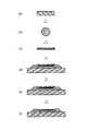
縦型構造の半導体デバイスを製造する一連の工程の概要を、図1に基づき説明する。図1において、(a)の工程では基板の上に半導体層が形成される。(b)の工程では基板と半導体層が1チップの大きさに分割される。(c)の工程では1チップに分割された基板と半導体層の側面に保護膜が形成される。また、電極が形成される。(d)の工程では側面に保護膜が形成された基板と半導体層が貼り付け材料層を介して支持基板に貼り付けられる。(e)の工程では保護層が除去される。(f)の工程では半導体層から基板が分離される。 An outline of a series of steps for manufacturing a semiconductor device having a vertical structure will be described with reference to FIG. In FIG. 1, a semiconductor layer is formed on a substrate in the step (a). In the step (b), the substrate and the semiconductor layer are divided into the size of one chip. In the step (c), a protective film is formed on the side surfaces of the substrate and the semiconductor layer divided into one chip. An electrode is also formed. In the step (d), the substrate having the protective film formed on the side surface and the semiconductor layer are attached to the supporting substrate through the attachment material layer. In the step (e), the protective layer is removed. In the step (f), the substrate is separated from the semiconductor layer.
基板とその上に形成される半導体層の構成例を図2に示す。図2の構成例では、サファイア基板などの基板11の上に、MOCVD法などの成長方法により、窒化物半導体層12が形成されている。窒化物半導体層12は複数の層によって構成される。複数の層とは、基板11に近い側より、バッファ層21、バッファ層22、n型半導体層23、発光層24、及びp型半導体層25である。バッファ層21は電磁放射線の吸収層となる。n型半導体層23とp型半導体層25は位置を入れ替えてもよい。 FIG. 2 shows a configuration example of the substrate and the semiconductor layer formed thereon. In the configuration example of FIG. 2, a
縦型構造の半導体デバイスの製造段階が図1の(f)の工程にまで進んだとき、基板11と窒化物半導体層12の界面に電磁放射線(図2ではブロック矢印が電磁放射線を象徴している)が照射される。電磁放射線はバッファ層21で吸収されて界面に熱が発生し、その熱で基板11と窒化物半導体層12が分離する。電磁放射線がレーザー光であればレーザーリフトオフ法の実践ということになる。 When the manufacturing process of the semiconductor device having the vertical structure has advanced to the process of FIG. 1F, electromagnetic radiation (block arrows in FIG. 2 symbolizes electromagnetic radiation at the interface between the
基板11としては、電磁放射線を吸収しにくく、電磁放射線の透過率が大きいものが好ましい。サファイアは150nmから1000nmにわたる広い波長域で高い透過率を有しており、基板11の材料として好適である。 The
基板11の裏面(窒化物半導体層12が形成される面と反対側の面)から電磁放射線の照射が行われるため、基板11の裏面は粗面のままとしないのがよい。その上で、光の散乱を抑えるべく、基板11と空気との界面での反射を少なくする処理を施すのがよい。そのような処理としては、基板11を研磨して薄くした後、鏡面とするための研磨工程や、基板11の裏面にARコーティング処理(anti-reflective coating)を施したりすることが推奨される。 Since electromagnetic radiation is applied from the back surface of the substrate 11 (the surface opposite to the surface on which the
半導体層から基板を分離する(f)の工程以前に、基板を研磨工程などにより、100μm程度まで薄くする工程が含まれていても良い。この場合、研磨工程は、保護膜が除去される(e)の工程の前に実施すると良い。なぜなら、保護膜が除去された空間に、研磨工程で発生するゴミが入るのを防ぐ事ができるからである。 Before the step (f) of separating the substrate from the semiconductor layer, a step of thinning the substrate to about 100 μm by a polishing step or the like may be included. In this case, the polishing step is preferably performed before the step (e) in which the protective film is removed. This is because dust generated in the polishing process can be prevented from entering the space from which the protective film has been removed.
電磁放射線の波長がバッファ層21よりもバンドギャップの大きい波長であると、バッファ層21と基板11の界面で電磁放射線の吸収とそれに伴う熱分解が起こり、発熱が生じる。この熱が基板11の分離を招く。バッファ層21として好適する物質が何であるかは窒化物半導体層12の構成によって左右される。 If the wavelength of the electromagnetic radiation is a wavelength having a band gap larger than that of the
窒化物半導体層12が発光デバイスを形成するのに用いられる場合、どの波長の光を出力することを目指すかによって窒化物半導体層12の構成が異なってくる。それに伴いバッファ層21として適する物質も異なってくる。 When the
360nmよりも短い波長の光の出力を目指す窒化物半導体層12であれば、Alを含有する物質の層を中心とした構成になるため、バッファ層21をAlNとするのがよい。サファイア基板上に形成されたAlNにおいて、AlNとサファイア基板の界面付近のAlN層は一般的に欠陥を多く有し、欠陥が多ければより効率的に光を吸収するので、その意味でもAlNはバッファ層21に適すると言える。 In the case of the
青紫色(405nm)、青色(450nm)、緑色(525nm)などといった、360nmよりも長い波長の光の出力を目指す窒化物半導体層12であれば、バッファ層21はGaNとするのがよい。サファイア基板上に形成されたGaNにおいて、GaNとサファイア基板の界面付近のGaN層は一般的に欠陥を多く有し、欠陥が多ければより効率的に光を吸収する。その意味でもGaNはバッファ層21に適すると言える。 If the
基板11の上に形成される窒化物半導体層12の構成例を図3に示す。基板11は両面研磨を施したサファイア基板であり、その上にAlNバッファ層31、ノンドープAlN層32、ノンドープAlGaN層33、n型AlGaN層34、活性層35、キャリアバリア層36、p型AlGaN層37、及びp型GaNコンタクト層38からなる窒化物半導体層12が形成されている。 A configuration example of the
ノンドープAlN層32の厚さは約3μmである。ノンドープAlGaN層33はAl0.50Ga0.50Nからなり、厚さは約1.0μmである。n型AlGaN層34もAl0.50Ga0.50Nからなり、厚さは約2.0μmである。キャリアバリア層36はp型Al0.75Ga0.25Nからなり、厚さは約15nmである。p型AlGaN層37はp型Al0.50Ga0.50Nからなり、厚さは約10nmである。p型GaNコンタクト層38の厚さは約15nmである。 The thickness of the
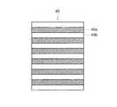
活性層35は、図4に示す通り、量子井戸層35aと障壁層35bとが交互に積層された量子井戸構造を備えている。量子井戸層35aはAl0.401Ga0.60Nからなる。障壁層35bはAl0.601Ga0.40Nからなり、量子井戸数は5である。 As shown in FIG. 4, the
図3に示した窒化物半導体層12の形成にあたっては、MOCVD(metal organic chemical vapor deposition)などのエピタキシャル成膜方法が用いられる。 In forming the
窒化物半導体層12から基板11を分離する電磁放射線の発生源はエキシマレーザーとされる。エキシマレーザー光として通常用いられるのは波長193nmのArFエキシマレーザー光か波長248nmのKrFエキシマレーザー光である。 The source of electromagnetic radiation that separates the
図2に示す構成の窒化物半導体層12であって、バッファ層21がAlNである場合には、波長248nmのKrFエキシマレーザー光を用いると、図6に示す通り、基板11とバッファ層21の界面でKrFエキシマレーザー光の吸収が生じず、KrFエキシマレーザー光はバッファ層21を抜けてさらに窒化物半導体層12の奥深くまで浸透する。そのような場所でKrFエキシマレーザー光が吸収され、熱分解が生じると、発光層24がダメージを受けるおそれがあり、好ましくない。図6中に描かれた、破線で囲んだ矩形であって、ハッチングを施していないものは、その領域で発熱が生じていないことを象徴している。 When the
そこで、バッファ層21がAlNである場合には、波長193nmのArFエキシマレーザー光(図5参照)が使用される。波長193nmのArFエキシマレーザー光であれば、基板11とバッファ層21の界面でArFエキシマレーザー光が吸収されて発熱が生じ、基板11を分離することができる。図5中に描かれたハッチングを施した矩形はその領域における発熱を象徴している。 Therefore, when the
ArFエキシマレーザー光の設定条件の一例を以下に示す。パルス幅は20ナノ秒とする。照射面積は、メタルマスクまたはフォトマスクで整形を行い、500μm角とする。エネルギー密度は1000〜5000mJ/cm2とする。この設定条件のArFエキシマレーザー光を500μm角の照射エリアに1〜5パルス照射しては移動させるステップアンドリピートにより、5mm角といったウェハーサイズの窒化物半導体層12の全面をArFエキシマレーザー光で照射する。An example of setting conditions for ArF excimer laser light is shown below. The pulse width is 20 nanoseconds. The irradiation area is shaped with a metal mask or a photomask and is 500 μm square. The energy density is 1000 to 5000 mJ / cm2 . IrF excimer laser light having a set size of 5 μm square is irradiated with ArF excimer laser light by step-and-repeat that moves by irradiating an ArF excimer laser light of 500 μm square with 1 to 5 pulses. To do.
ステップアンドリピートによるレーザー照射の概念を図8及び図9に示す。図8はチップ形状が角形の場合、図9はチップ形状が円形の場合である。図8及び図9で上方に示した例のように、照射エリア同士を互いの間に重なりが生じないように隣接させてレーザー照射してもよく、図8及び図9で下方に示した例のように、照射エリア同士を互いの間に重なりが生じる形で連続させてレーザー照射してもよい。 The concept of laser irradiation by step-and-repeat is shown in FIGS. FIG. 8 shows a case where the chip shape is square, and FIG. 9 shows a case where the chip shape is circular. As in the example shown above in FIGS. 8 and 9, the laser irradiation may be performed with the irradiation areas adjacent to each other so as not to overlap each other, and the example shown in the bottom in FIGS. 8 and 9. As described above, the laser irradiation may be performed in such a manner that the irradiation areas are continuously formed so as to overlap each other.
図2に示す構成の窒化物半導体層12であって、バッファ層21がGaNである場合は、波長248nmのKrFエキシマレーザー光(図7参照)が使用される。図7中に描かれたハッチングを施した矩形はその領域における発熱を象徴している。 In the case of the
KrFエキシマレーザー光の設定条件の一例を以下に示す。パルス幅は30ナノ秒とする。照射面積は、メタルマスクまたはフォトマスクで整形を行い、0.8mm角とする。エネルギー密度は700mJ/cm2とする。この設定条件のKrFエキシマレーザー光を0.8mm角の照射エリアに1パルス照射しては移動させる図8または図9に示すようなステップアンドリピートにより、6mm角といったウェハーサイズの窒化物半導体層12の全面をKrFエキシマレーザー光で照射する。An example of setting conditions for KrF excimer laser light is shown below. The pulse width is 30 nanoseconds. The irradiation area is shaped with a metal mask or a photomask and is 0.8 mm square. The energy density is 700 mJ / cm2 . A step-and-repeat as shown in FIG. 8 or FIG. 9 in which a KrF excimer laser beam of this setting condition is irradiated and moved by irradiating a pulse area of 0.8 mm square with a single pulse, and a
窒化物半導体層12が形成される基板11としては、例えば直径が2インチサイズであるサファイア基板が用いられる。このような寸法の基板11は、窒化物半導体層12の形成が完了した後、窒化物半導体層12共々1チップのサイズに分割される。 As the
1チップサイズは、例えば1辺の長さが0.3mm程度の正方形とすることができる。窒化物半導体層12を発光デバイスとして用いる場合、大出力化のためには発光面積の拡大、すなわちチップサイズの拡大が有効である。例えば1辺の長さが0.5mm以上や1mm以上といったチップサイズにすればよい。チップサイズの拡大には、レジスト塗布工程で均一塗布が容易になるというメリットもある。1辺の長さが5mm以上というチップサイズにすれば、レジスト塗布の容易化に加えて、チップのハンドリングが容易になり、スループットが向上するというメリットももたらされる。さらに、1辺の長さが1cm程度というチップサイズにすれば、大出力になることは当然であるが、基板の分離が容易といったメリットも生まれる。 One chip size may be a square having a side length of about 0.3 mm, for example. When the
基板11と窒化物半導体層12を1チップサイズに分割するのは、レーザースクライブ法などを用いて行われる。図10と図11に2通りの分割手順を示す。 The
図10に示す手順は、窒化物半導体層12に対しp型化熱処理を行った段階で分割し、その後、分割後のチップに対しp電極を蒸着するというものである。この手順によると、金属蒸着膜が分割されないので、金属蒸着膜の端にダレが発生しない。またウェハーサイズが大きいと熱処理に伴うウェハーの反りも大きく、電極剥がれなどの問題を生じるが、ウェハーを分割してから電極を蒸着するという手順であれば、そのような問題の発生を避けられる。 The procedure shown in FIG. 10 is to divide the
図11に示す手順は、窒化物半導体層12に対しp型化熱処理とp電極の蒸着を済ませた後に分割するというものである。この手順によれば1回の処理で多くのチップを産出することができ、スループットが向上する。金属蒸着膜のダレの問題に関しては、分割箇所の金属蒸着膜を除去しておいてから分割することで問題を解決できる。 The procedure shown in FIG. 11 is to divide the
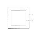
基板11と窒化物半導体層12のチップ形状は、図15に示す角形(正方形や矩形)に限定されない。図16に示す円形であってもよい。チップ形状を円形とすることのメリットは後で説明する。 The chip shape of the
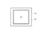
上記のように1チップサイズに分割した基板11と窒化物半導体層12は、図1の(d)の工程で支持基板13(図12参照)に貼り付けられる。大面積の支持基板13にチップサイズに分割する前の基板11と窒化物半導体層12のチップを貼り付け、基板11を分離した後に、窒化物半導体層12と支持基板13を分割するという手順もあり得るが、それは、基板11を分離されて極薄膜となった窒化物半導体層12に対し支持基板分割時の応力が及び、結晶品質の劣化を招くおそれがあり、好ましくない。 The
そこで、支持基板13の方も基板11と窒化物半導体層12のチップサイズに見合ったサイズに予め加工しておくのがよい。基板11と窒化物半導体層12のチップサイズが5mm角であれば、支持基板13は1辺が5mm以上の角形ということになる。窒化物半導体層12に対してワイヤーボンディングが行われる場合は、支持基板13はワイヤーを張る領域も含めたサイズとする必要がある。また支持基板13のサイズを決めるにあたっては放熱性も考慮しなければならない。製造工程でのハンドリングの容易性や、使用時の放熱性などを考慮すれば、例えば、基板11と窒化物半導体層12が1辺1mm以下の角形であっても、支持基板13は1辺3mm以上の角形であるとより好ましい。 Therefore, the
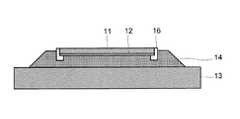
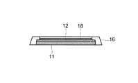
図12及び図13に示す支持基板13に対する基板11と窒化物半導体層12の組み合わせ態様では、支持基板13の上にパッド電極15が形成され、パッド電極15の上に貼り付け材料層14が形成されているが、パッド電極15を介さず支持基板13の上に直接貼り付け材料層14が形成されることもある。図22から図24に示す実施形態では支持基板13の上に直接貼り付け材料層14が形成された状態が描かれている。いずれにせよ、貼り付け材料層14に窒化物半導体層12が貼り付けられるのであるが、その前に踏むべき手順がある。それは図1の(c)の工程、すなわち1チップに分割された基板11と半導体層12の側面に保護膜を形成するという工程である。 In the combination mode of the
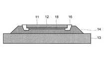
図14には1チップに分割された基板11と窒化物半導体層12の側面に保護膜16が形成された状態が示されている。保護膜16としては例えばSiO2が用いられる。保護膜16の形成にあたっては、基板11と窒化物半導体層12の側面にも成膜が可能な成膜装置を用いる。FIG. 14 shows a state in which the
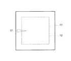
保護膜16を形成するに際し、基板11と窒化物半導体層12を保持するやり方には2通りある。その1は、図17及び図18に示すように、基板11が下で窒化物半導体層12が上の状態、すなわちフェイスアップの状態とするやり方である。その2は、図19及び図20に示すように、窒化物半導体層12が下で基板11が上の状態、すなわちフェイスダウンの状態とするやり方である。 There are two ways to hold the
フェイスダウンでは窒化物半導体層12を下から治具17で支える。そのため、窒化物半導体層12の表面に保護膜16が形成されない部分が生じる。その部分が窒化物半導体層12の側面であると、本発明の効果が減殺されてしまう。従って、保護膜形成時には基板11と窒化物半導体層12をフェイスアップで支持しておくのがよい。 In face-down, the
窒化物半導体層12の上面における保護膜16の厚さは3μmとすることができる。保護膜16は窒化物半導体層12と共に貼り付け材料層14に埋め込まれるので、保護膜16の存在が基板11と窒化物半導体層12の反りに悪影響を及ぼすといった事態は、基本的には発生しない。しかしながら保護膜16が厚ければそのような悪影響が生じる可能性を排除できない。また保護膜16を誘電体膜とした場合、保護膜16が厚ければ形成に時間がかかり、生産性が悪化する。それらを考慮すると、窒化物半導体層12の上面における保護膜16の厚さは5μm以下にするのがよい。 The thickness of the
基板11と窒化物半導体層12の側面における保護膜16の厚さは、窒化物半導体層12の上面における保護膜16の厚さよりも厚くする。すなわち図15及び図16に示すように、窒化物半導体層12の上面における保護膜16の厚さが5μm以下であるならば、基板11と窒化物半導体層12の側面における保護膜16の厚さは5μm以上とする。図15は基板11が角形である場合、図16は基板11が円形である場合を示す。 The thickness of the
それが可能であるならば、基板11と窒化物半導体層12の側面に50μm程度の厚さの保護膜16を形成することもできる。基板11と窒化物半導体層12の側面に形成された保護膜16が厚ければ、貼り付け材料層14に対し後述の処理を行うとき、処理が楽である。 If this is possible, a
基板11と窒化物半導体層12を1チップサイズに分割する工程の説明のところで触れた、窒化物半導体層12に対するp電極の蒸着は、保護膜16を形成した後に行うこともできる。その時は保護膜を形成した基板11と窒化物半導体層12をフェイスダウンの状態で支持しておいてp電極の蒸着を行う。窒化物半導体層12を下から支える治具と窒化物半導体層12の間に保護膜16が介在するので、治具と窒化物半導体層12の間には隙間が生じている。このため、保護膜16から露出している窒化物半導体層12の全面に、治具によって邪魔されることなくp電極を蒸着することができる。この場合、保護膜16を、蒸着金属による被覆領域を画定する手段として利用することができる。 The deposition of the p-electrode on the
上記のように保護膜16を形成した後、基板11と窒化物半導体層12を支持基板13上の貼り付け材料層14に加熱圧着で貼り付ける。すなわち図1の(d)の工程を遂行する。そのために基板11と窒化物半導体層12を、図21に示す通り、窒化物半導体層12が下で基板11が上の状態に置く。 After forming the
次いで図22に示す通り、窒化物半導体層12と基板11、及びそれらを囲む保護膜16を貼り付け材料層14に加熱圧着する。 Next, as shown in FIG. 22, the
貼り付け材料層14の厚さは10μm以上とするのがよい。50μmであればより好ましい。100μm以上であってもよい。このように貼り付け材料層14はある程度の厚さを有していることが求められる。しかしながら厚すぎるのは材料コストの観点から好ましくない。そこで、例えば500μmといった値を貼り付け材料層14の厚さの上限として設定することができる。尚、ここでの厚さとは、加熱圧着処理された後の窒化物半導体層12と支持基板13の間ではなく、それ以外の部分の、接着材料の厚さを意味する。 The thickness of the
窒化物半導体層12と基板11、及び保護膜16を貼り付け材料層14に上から押し付けると、窒化物半導体層12と基板11、及び保護膜16は貼り付け材料層14の中に沈み込み、逆に貼り付け材料層14は窒化物半導体層12と基板11、及び保護膜16の外側に盛り上がる。貼り付け材料層14の厚さの方が窒化物半導体層12の厚さよりも大であれば、貼り付け材料層14の盛り上がりは基板11の側面にまで達する。もし保護膜16が存在していなかったら、基板11の側面に貼り付け材料層14が付着してしまうところであるが、保護膜16が存在するため、そのような事態は避けられる。 When the
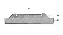
次いで図23に示す通り保護膜16を除去する。保護膜16がSiO2で形成されていれば、フッ素系溶液により保護膜16を溶解することができる。これにより、貼り付け材料層14の中で保護膜16が存在した箇所は空間と化す。Next, as shown in FIG. 23, the
次いで基板11と窒化物半導体層12の界面に電磁放射線を照射してその界面で基板11と窒化物半導体層12を分離し、基板11を分離する。前述の通り、貼り付け材料層14の中で保護膜16が存在した箇所は空間と化しており、基板11と貼り付け材料層14は接触していない。このため、基板11は貼り付け材料層14によって阻害されることなく分離される。基板分離後の状態は図24に示す通りである。その後、支持基板13と貼り付け材料層14、及び窒化物半導体層12は次工程に送られる。 Next, electromagnetic radiation is applied to the interface between the
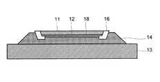
図25には窒化物半導体層12の表面に電極18が形成されている状態が描かれている。基板11、窒化物半導体層12、及び電極18の周囲に保護膜16を形成し、それらを支持基板13上の貼り付け材料層14に加熱圧着し(図26参照)、保護膜16を除去し(図27参照)、基板11を分離すると、貼り付け材料層14の上に電極18と窒化物半導体層12がとり残される(図28参照)。その後、支持基板13と貼り付け材料層14、及び窒化物半導体層12と電極18は次工程に送られる。 FIG. 25 illustrates a state in which the
図29には図25と同様に表面に電極18が形成された窒化物半導体層12と基板11が描かれているが、その窒化物半導体層12と基板11、及び保護層16は次のような形状とされている。すなわち窒化物半導体層12は基板11に接する面よりもその反対側の面の方が面積小となるように側面が傾斜した形にされる。基板11は、窒化物半導体層12に接する面よりもその反対側の面の方が面積大となるように側面が傾斜した形にされる。窒化物半導体層12の側面の傾斜角度と基板11の側面の傾斜角度は等しくされる。保護膜16の側面にも窒化物半導体層12及び基板11の側面の傾斜角度と同じ傾斜角度が生じる。 FIG. 29 shows the
上記のように側面が傾斜している基板11、窒化物半導体層12、及び保護膜16を支持基板13上の貼り付け材料層14に加熱圧着し(図30参照)、保護膜16を除去(図31参照)すると、貼り付け材料層14の中で保護膜16が存在していた空間に傾斜面14aが生じる。上記のように基板11の側面と窒化物半導体層12の側面の両方が同じように傾斜していると、傾斜面の面積が大きいため、貼り付け材料層14への形状転写効果が大きいというメリットがある。 The
その後基板11を分離すると、貼り付け材料層14の上に電極18と窒化物半導体層12がとり残される(図32参照)。 Thereafter, when the
窒化物半導体層12が発光デバイスに用いられる場合、窒化物半導体層12から出射される光は、大半が窒化物半導体層12の主平面からそれと垂直方向に出射される。そのような主たる光が図33において上向きのブロック矢印で象徴されている。しかしながら、窒化物半導体層12の側面から側方に、図33では水平方向に、出射する光も一部存在する。そのような光は傾斜面14aに当たり、保護膜除去後の空間の外側へと反射される。この反射光が前記主たる光に加わることで、光の利用効率が向上する。 When the
図34には図29に描かれた形状を少し変化させた形状が描かれている。ここでは、表面に電極18が形成された窒化物半導体層12は基板11に接する面よりもその反対側の面の方が面積小となるように側面が傾斜した形とされているが、基板11の側面は垂直のままとされている。保護膜16の側面には窒化物半導体層12の側面の傾斜角度と同じ傾斜角度がつけられている。 FIG. 34 shows a shape obtained by slightly changing the shape shown in FIG. Here, the
上記の基板11、窒化物半導体層12、及び保護膜16を支持基板13上の貼り付け材料層14に加熱圧着し(図35参照)、保護膜16を除去(図36参照)すると、貼り付け材料層14の中で保護膜16が存在していた空間に傾斜面14aが生じる。その後基板11を分離すると、貼り付け材料層14の上に電極18と窒化物半導体層12がとり残される(図37参照)。窒化物半導体層12が発光デバイスに用いられる場合、窒化物半導体層12の側面から側方に出射した光は、図33に示したのと同様に傾斜面14aに当たって図の上方に反射され、窒化物半導体層12の主平面からそれと垂直方向に出射される主たる光に加わる。これにより、光の利用効率が向上する。 The
保護膜除去後に窒化物半導体層12の側面に対峙する面、すなわち傾斜面14aは、光を効率的に取り出すため、光反射率が高い方がよい。そこで、次のようして傾斜面14aの光反射率を高める。 The surface facing the side surface of the
第1の手段としては、貼り付け材料層14の材料に光反射率の高い材料を使用することが挙げられる。 As a first means, a material having a high light reflectance can be used as the material of the
光反射率の高い材料を貼り付け材料層14に用いることができないときは、図38に示す通り、傾斜面14aに光反射率の高い反射膜19を形成する。反射膜19はフォトリソグラフィーと金属蒸着で形成することができる。 When a material having a high light reflectance cannot be used for the
側面に傾斜をつけることを考えると、窒化物半導体層12と基板11のチップは平面形状が円形であることが望ましい。チップ形状が円形であればチップを回転させながら研磨することが可能になり、傾斜面形成の効率が上がり、スループットが向上する。 Considering that the side surfaces are inclined, it is desirable that the
チップ形状が角形であっても、1辺ずつ研磨することで傾斜をつけることができる。傾斜面の形成には、特開2009−262249号公報に記載されているような装置を用いることができる。 Even if the chip shape is square, it can be inclined by polishing one side at a time. An apparatus as described in JP 2009-262249 A can be used for forming the inclined surface.
チップ形状が角形である場合、電磁放射線の照射スポット形状を角形にすると、図8に示す通り、最小限の照射(ショット)でチップ全面を無駄なく照射することができる。チップ形状が円形である場合、照射スポット形状を角形にすると、端の部分の照射で無駄が生じる可能性がある。この場合は照射スポット形状を円形が好ましい。 When the chip shape is rectangular, if the irradiation spot shape of electromagnetic radiation is square, as shown in FIG. 8, the entire chip surface can be irradiated with minimal irradiation (shot) without waste. When the tip shape is circular, if the irradiation spot shape is a square shape, there is a possibility that waste is caused by irradiation of the end portion. In this case, the irradiation spot shape is preferably circular.
本発明の発明者は様々な実験を行って本発明の有用性を確かめた。以下、その実験で得られた知見を「実施例」として紹介する。 The inventors of the present invention conducted various experiments to confirm the usefulness of the present invention. In the following, the knowledge gained from the experiment will be introduced as an “Example”.
<実施例1>
2インチサイズのサファイア基板に、図3及び図4に示す構造の窒化物半導体層を形成した。その基板をレーザースクライブ法で6mm角のチップに分割した。チップ分割後、プラズマCVD法を用いて保護膜となるSiO2膜を1.5μmの厚さに蒸着した。窒化物半導体層の上面では端から50μmまでSiO2膜を形成した。その後、p電極としてPdを200nmとAuを1000nm、EB蒸着法で蒸着した。なお窒化物半導体層に接する電極材料としては、PdやAuの他、発光波長で反射率が高い材料、例えばAl、Ni、Ptなども好ましい。Alは最も反射率が高いので好ましい。NiやPtも比較的反射率が高くp型半導体とのコンタクト性能が良好なので好ましい。<Example 1>
A nitride semiconductor layer having the structure shown in FIGS. 3 and 4 was formed on a 2-inch sapphire substrate. The substrate was divided into 6 mm square chips by laser scribing. After dividing the chip, a SiO2 film serving as a protective film was deposited to a thickness of 1.5 μm using a plasma CVD method. On the top surface of the nitride semiconductor layer, a SiO2 film was formed from the end to 50 μm. Thereafter, Pd was vapor deposited by EB vapor deposition at 200 nm and Au at 1000 nm as a p-electrode. As the electrode material in contact with the nitride semiconductor layer, a material having high reflectance at the emission wavelength, such as Al, Ni, Pt, etc., is also preferable in addition to Pd and Au. Al is preferred because it has the highest reflectivity. Ni and Pt are also preferable because of their relatively high reflectivity and good contact performance with p-type semiconductors.
支持基板としてはゲルマニウムを10mm角に分割したものを用意した。貼り付け材料としてはSnを20質量%含有し、残りがAuからなるAuSnを用いた。支持基板の上にAuSnを置き、その上にSiO2保護膜を有するチップを置き、従来用いられているウェハーボンディング装置で貼り付けを行った。その後フッ素系溶液でSiO2保護膜を除去した。貼り付け材料の厚さは30μmであった。A support substrate prepared by dividing germanium into 10 mm squares was prepared. As the pasting material, AuSn containing 20% by mass of Sn and the remainder made of Au was used. AuSn was placed on a support substrate, a chip having a SiO2 protective film was placed thereon, and pasting was performed using a conventionally used wafer bonding apparatus. Thereafter, the SiO2 protective film was removed with a fluorine-based solution. The thickness of the pasting material was 30 μm.
続いてレーザーリフトオフでサファイア基板を分離した。光源は波長193nmのArFエキシマレーザー、パルス幅は20ナノ秒とした。照射面積は、メタルマスク若しくは、フォトマスクにより整形を行い、500μm角とした。照射エネルギー密度は2000mJ/cm2とした。Subsequently, the sapphire substrate was separated by laser lift-off. The light source was an ArF excimer laser with a wavelength of 193 nm, and the pulse width was 20 nanoseconds. The irradiation area was shaped by a metal mask or a photomask, and was 500 μm square. The irradiation energy density was 2000 mJ / cm2 .
500μm角である1照射エリアに1〜5パルス程度照射しては移動させるステップアンドリピートにより、5mm角のチップ全面に照射を行った。その結果、SiO2保護膜を形成していたチップではサファイア基板を10個中9個分離することができた。Irradiation was performed on the entire surface of a 5 mm square chip by step-and-repeat that moved by irradiating about 1 to 5 pulses to one irradiation area of 500 μm square. As a result, nine out of ten sapphire substrates could be separated from the chip on which the SiO2 protective film was formed.
SiO2保護膜を形成していなかったチップについても上記と同じ条件で、但しSiO2保護膜の除去というステップは踏まないで、実験を行ったが、その結果、サファイア基板を分離することができたのは10個中0個であった。殆どのサファイア基板の側壁にAuSnが付着していた。A chip that had not been formed with a SiO2 protective film was also tested under the same conditions as above, but without performing the step of removing the SiO2 protective film. As a result, the sapphire substrate could be separated. The number was 0 out of 10. AuSn adhered to the side wall of most sapphire substrates.
貼り付け材料の厚さのみを30μmから10μmに変え、上記の実験を繰り返した。その結果、SiO2保護膜を形成していたチップではサファイア基板を10個中10個分離することができた。SiO2保護膜を形成していなかったチップではサファイア基板を10個中2個しか分離することができなかった。サファイア基板を分離できた2個のチップでは、成長した窒化物半導体層の側面のみにAuSnが付着していた。Only the thickness of the pasting material was changed from 30 μm to 10 μm, and the above experiment was repeated. As a result, 10 out of 10 sapphire substrates could be separated from the chip on which the SiO2 protective film was formed. Only two of the ten sapphire substrates could be separated by a chip on which no SiO2 protective film was formed. In the two chips that were able to separate the sapphire substrate, AuSn was attached only to the side surface of the grown nitride semiconductor layer.
<実施例2>
2インチサイズのサファイア基板に、図3及び図4に示す構造の窒化物半導体層を形成した。その基板をレーザースクライブ法で10mm角のチップに分割した。分割後、窒化物半導体のチップとサファイア基板の両方の側面に図29に示すような傾斜面を形成した。それからプラズマCVD法を用いて保護膜となるSiO2膜を3.0μmの厚さに蒸着した。<Example 2>
A nitride semiconductor layer having the structure shown in FIGS. 3 and 4 was formed on a 2-inch sapphire substrate. The substrate was divided into 10 mm square chips by laser scribing. After the division, inclined surfaces as shown in FIG. 29 were formed on the side surfaces of both the nitride semiconductor chip and the sapphire substrate. Then, a SiO2 film serving as a protective film was deposited to a thickness of 3.0 μm using a plasma CVD method.
支持基板にはAlN基板を用いた。その表面にはパッド電極を形成した。なお、パッド電極の材料としてはTi/AuやNi/Auなどを用いることができる。 An AlN substrate was used as the support substrate. A pad electrode was formed on the surface. In addition, Ti / Au, Ni / Au, etc. can be used as a material of a pad electrode.
貼り付け材料としては熱可塑性樹脂を用いた。厚さは約50μmとした。貼り付け材料の上にSiO2保護膜を有するチップを置き、従来用いられているウェハーボンディング装置で貼り付けを行った。その後フッ素系溶液でSiO2保護膜を除去した。A thermoplastic resin was used as the pasting material. The thickness was about 50 μm. A chip having a SiO2 protective film was placed on the pasting material, and pasting was performed by a conventionally used wafer bonding apparatus. Thereafter, the SiO2 protective film was removed with a fluorine-based solution.
続いて貼り付け材料層に貼り付けたチップからレーザーリフトオフでサファイア基板を分離した。光源はArFエキシマレーザー、パルス幅は20ナノ秒とした。照射面積は、メタルマスク若しくは、フォトマスクにより整形を行い、1000μm角とした。照射エネルギー密度は2500mJ/cm2とした。Subsequently, the sapphire substrate was separated from the chip attached to the attachment material layer by laser lift-off. The light source was an ArF excimer laser, and the pulse width was 20 nanoseconds. The irradiation area was shaped by a metal mask or a photomask, and was 1000 μm square. The irradiation energy density was 2500 mJ / cm2 .
1000μm角である1照射エリアに1〜3パルス程度照射しては移動させるステップアンドリピートにより、12mm角のチップ全面に照射を行った。その結果、SiO2保護膜を形成していたチップでは全サンプルでサファイア基板を分離することができた。Irradiation was performed on the entire surface of a 12 mm square chip by step-and-repeat that moved by irradiating about 1 to 3 pulses to one irradiation area of 1000 μm square. As a result, it was possible to separate the sapphire substrate from all samples in the chip on which the SiO2 protective film was formed.
後でその一例を示すn−AlGaN頭だしエッチングを行い、電極を形成し、電流注入による光出力特性について検討した。 Later, n-AlGaN head etching as an example was performed to form electrodes, and the light output characteristics by current injection were examined.
窒化物半導体のチップとサファイア基板の両方の側面に図29に示すような傾斜面を形成した結果、貼り付け材料に傾斜面を形成しない場合(比較サンプル)に比べて光出力が約1.6倍になったことを確認できた。このような結果が得られたのは、窒化物半導体チップから横方向に出射する光を有効に取り出せたことに起因すると考えられる。 As a result of forming the inclined surfaces as shown in FIG. 29 on both side surfaces of the nitride semiconductor chip and the sapphire substrate, the light output is about 1.6 as compared with the case where the inclined surface is not formed on the bonding material (comparative sample). I was able to confirm that it doubled. The reason why such a result was obtained is considered to be due to the effective extraction of light emitted from the nitride semiconductor chip in the lateral direction.
<実施例3>
2インチサイズのサファイア基板に、図39及び図40に示す構造の窒化物半導体層を形成した。図39において、基板11は両面研磨を施したサファイア基板であり、その上に低温GaNバッファ層41、ノンドープGaN層42、n型GaN層43、バッファ層44、活性層45、キャリアバリア層46、p型GaN層47、及びp型GaNコンタクト層48からなる窒化物半導体層12が形成されている。<Example 3>
A nitride semiconductor layer having a structure shown in FIGS. 39 and 40 was formed on a 2-inch sapphire substrate. In FIG. 39, the
低温GaNバッファ層41の厚さは約100nm、ノンドープGaN層42の厚さは約4μm、n型GaN層43の厚さは約2μm、バッファ層44の厚さは約0.6μm、キャリアバリア層46の厚さは約15nm、p型GaN層47の厚さは約80nm、p型GaNコンタクト層48の厚さは約20nmである。 The low-temperature
キャリアバリア層46はp型AlGaNからなる。バッファ層44は約1.5nmのノンドープGaNと約1.5nmのノンドープIn0.03Ga0.97Nからなる超格子構造を備える。The
活性層45は、図40に示す通り、量子井戸層45aと障壁層45bとが交互に積層された量子井戸構造を備えている。量子井戸層45aは、約3.5nmの厚さを有するノンドープIn0.16Ga0.84Nよりなる井戸層と、約15nmの厚さを有するノンドープGaNよりなる障壁層を6周期積層した6量子井戸構造を備える。As shown in FIG. 40, the
図39に示した窒化物半導体層12の形成にあたっては、MOCVD(metal organic chemical vapor deposition)などのエピタキシャル成膜方法が用いられる。 In forming the
図30の基板11をレーザースクライブ法で6mm角のチップに分割した。チップ分割後、プラズマCVD法を用いて保護膜となるSiO2膜を1.5μmの厚さに蒸着した。窒化物半導体層の上面では端から50μmまでSiO2膜を形成した。その後、p電極としてPdを200nmとAuを1000nm、EB蒸着法で蒸着した。なお窒化物半導体層に接する電極材料としては、PdやAuの他、発光波長で反射率が高い材料、例えばAl、Ni、Ptなども好ましい。Alは最も反射率が高いので好ましい。NiやPtも比較的反射率が高くp型半導体とのコンタクト性能が良好なので好ましい。The
支持基板としてはシリコン基板を10mm角に分割したものを用意した。貼り付け材料としてはSnを20質量%含有し、残りがAuからなるAuSnを用いた。貼り付け材料の厚さは30μmとした。支持基板の上にAuSnを置き、その上にSiO2保護膜を有するチップを置き、従来用いられているウェハーボンディング装置で貼り付けを行った。その後フッ素系溶液でSiO2保護膜を除去した。A support substrate prepared by dividing a silicon substrate into 10 mm squares was prepared. As the pasting material, AuSn containing 20% by mass of Sn and the remainder made of Au was used. The thickness of the pasting material was 30 μm. AuSn was placed on a support substrate, a chip having a SiO2 protective film was placed thereon, and pasting was performed using a conventionally used wafer bonding apparatus. Thereafter, the SiO2 protective film was removed with a fluorine-based solution.
続いてAuSnに貼り付けたチップからレーザーリフトオフでサファイア基板を分離した。光源は波長238nmのKrFエキシマレーザー、パルス幅は30ナノ秒とした。照射面積は、マスクにより整形して0.8mm角とした。照射エネルギー密度は700mJ/cm2とした。0.8mm角である1照射エリアに1パルス照射しては移動させるというステップアンドリピートにより、6mm角のチップ全面に照射を行った。その結果、SiO2保護膜を形成していたチップではサファイア基板を10個中10個分離することができた。SiO2保護膜を形成していなかったチップについても上記と同じ条件で、但しSiO2保護膜の除去というステップは踏まないで、実験を行ったが、その結果は10個中2個からしかサファイア基板を分離することができなかった。分離できた2個のサファイア基板はいずれも側壁にAuSnが付着していないものであった。Subsequently, the sapphire substrate was separated from the chip attached to AuSn by laser lift-off. The light source was a KrF excimer laser with a wavelength of 238 nm, and the pulse width was 30 nanoseconds. The irradiation area was shaped with a mask to a 0.8 mm square. The irradiation energy density was 700 mJ / cm2 . Irradiation was performed on the entire surface of a 6 mm square chip by a step-and-repeat process of irradiating and moving one pulse to an irradiation area of 0.8 mm square. As a result, 10 out of 10 sapphire substrates could be separated from the chip on which the SiO2 protective film was formed. A chip that had not been formed with a SiO2 protective film was also tested under the same conditions as above, except that the step of removing the SiO2 protective film was not performed. The substrate could not be separated. The two sapphire substrates that could be separated had no AuSn attached to the side walls.
貼り付け材料の厚さのみを30μmから10μmに変え、上記の実験を繰り返した。その結果、SiO2保護膜を形成していたチップではサファイア基板を10個中10個分離することができた。SiO2保護膜を形成していなかったチップではサファイア基板を10個中4個しか分離することができなかった。サファイア基板を分離できた4個のチップでは、成長した窒化物半導体層の側面のみにAuSnが付着していた。Only the thickness of the pasting material was changed from 30 μm to 10 μm, and the above experiment was repeated. As a result, 10 out of 10 sapphire substrates could be separated from the chip on which the SiO2 protective film was formed. Only 4 out of 10 sapphire substrates could be separated by a chip on which no SiO2 protective film was formed. In the four chips that could separate the sapphire substrate, AuSn was attached only to the side surface of the grown nitride semiconductor layer.
<実施例4>
2インチサイズのサファイア基板に、図39及び図40に示す構造の窒化物半導体層を形成した。その基板をレーザースクライブ法で10mm角のチップに分割した。分割後、窒化物半導体のチップとサファイア基板の両方の側面に図29に示すような傾斜を形成した。それからプラズマCVD法を用いて保護膜となるSiO2膜を3.0μmの厚さに蒸着した。<Example 4>
A nitride semiconductor layer having a structure shown in FIGS. 39 and 40 was formed on a 2-inch sapphire substrate. The substrate was divided into 10 mm square chips by laser scribing. After the division, slopes as shown in FIG. 29 were formed on both sides of the nitride semiconductor chip and the sapphire substrate. Then, a SiO2 film serving as a protective film was deposited to a thickness of 3.0 μm using a plasma CVD method.
支持基板にはAlN基板を用いた。その表面にはパッド電極を形成した。なお、パッド電極の材料としてはTi/AuやNi/Auなどを用いることができる。 An AlN substrate was used as the support substrate. A pad electrode was formed on the surface. In addition, Ti / Au, Ni / Au, etc. can be used as a material of a pad electrode.
貼り付け材料としては熱可塑性樹脂を用いた。厚さは約50μmとした。貼り付け材料の上にSiO2保護膜を有するチップを置き、従来用いられているウェハーボンディング装置で貼り付けを行った。その後フッ素系溶液でSiO2保護膜を除去した。A thermoplastic resin was used as the pasting material. The thickness was about 50 μm. A chip having a SiO2 protective film was placed on the pasting material, and pasting was performed by a conventionally used wafer bonding apparatus. Thereafter, the SiO2 protective film was removed with a fluorine-based solution.
続いて貼り付け材料層に貼り付けたチップからレーザーリフトオフでサファイア基板を分離した。光源はKrFエキシマレーザー、照射面積はマスクにより整形して2.0mm角とした。照射エネルギー密度は800mJ/cm2とした。Subsequently, the sapphire substrate was separated from the chip attached to the attachment material layer by laser lift-off. The light source was a KrF excimer laser, and the irradiation area was shaped by a mask to a 2.0 mm square. The irradiation energy density was 800 mJ / cm2 .
実施例3と同様、SiO2保護膜を形成していたチップではサファイア基板を全て分離することができた。As in Example 3, the sapphire substrate was completely separated from the chip on which the SiO2 protective film was formed.
サファイア基板分離後に残された貼り付け材料層は、傾斜した光反射面を有する。この構成は、そのような光反射面を持たない構成に比べ、光出力が1.4倍程度増大した。これは、横方向の光の取り出しを効率良く行うことができたことによるものと考えられる。 The pasting material layer left after the sapphire substrate separation has an inclined light reflecting surface. In this configuration, the light output is increased by about 1.4 times compared to the configuration having no light reflecting surface. This is considered to be due to the fact that the light in the lateral direction can be extracted efficiently.
尚、サファイア基板分離後の処理としては、ノンドープのGaN層に対し、RIEやICPを用いたドライエッチングや、KOH溶液やNaOH、水酸化テトラアンモニウム(PMAH)などのアルカリ性溶液を用いたウェットエッチングで、n型GaNの頭出しを行うことができる。 In addition, as a process after separation of the sapphire substrate, dry etching using RIE or ICP or wet etching using an alkaline solution such as KOH solution, NaOH, tetraammonium hydroxide (PMAH) is performed on the non-doped GaN layer. Cueing of n-type GaN can be performed.
サファイア基板分離後の処理として、本発明ではICPドライエッチングを行った。その際、貼り付け材料層に接触していなかった部分が除去された。これはレーザー光照射の際、貼り付け材料層と空気の放熱性の違いにより、貼り付け材料層に接した部分と接していない部分とで温度分布に差が生じ、貼り付け材料層に接触していなかった部分にクラックが生じて強度が低下したため、エッチング中に除去されたものと考えられる。 In the present invention, ICP dry etching was performed as the treatment after the sapphire substrate separation. At that time, the portion that was not in contact with the adhesive material layer was removed. This is due to the difference in temperature distribution between the part that is in contact with the adhesive material layer and the part that is not in contact with the adhesive material layer due to the difference in heat dissipation of the adhesive material layer and air during laser irradiation. It is considered that cracks were generated in the portions that were not present and the strength was reduced, so that they were removed during etching.
エッチング工程の後で、エッチングによるダメージを除去するため、熱処理を行うこともできる。その後、n電極として、AlやTi、Mo、Auなどを含有する電極材料を蒸着する。n電極は、光取り出しの観点から、全面蒸着ではなく、メッシュ形状とすることも可能である。また貼り付け材料層の光反射面の反射率を高めるため、Alなどの金属材料を蒸着する。 After the etching process, heat treatment can be performed in order to remove damage caused by etching. Thereafter, an electrode material containing Al, Ti, Mo, Au or the like is deposited as an n-electrode. The n-electrode can be formed in a mesh shape instead of vapor deposition from the viewpoint of light extraction. In addition, a metal material such as Al is vapor-deposited in order to increase the reflectance of the light reflecting surface of the adhesive material layer.
図41には、貼り付け材料層に光反射面を有する半導体デバイスを形成する一連の工程が示されている。図41において、(a)の工程では基板の上に半導体層が形成される。(b)の工程では基板と半導体層が1チップの大きさに分割される。(c)の工程では基板と半導体層の側面に傾斜が形成される。(d)の工程では側面が傾斜した基板と半導体層に保護膜が形成され、保護膜の側面も傾斜面とされる。(e)の工程では半導体層の表面に電極が形成される。(f)の工程では側面に保護膜が形成された基板と半導体層が支持基板上の貼り付け材料層に貼り付けられる。(g)の工程では保護層が除去される。(h)の工程では半導体層から基板が分離される。(i)の工程では半導体層の側面が垂直にされる。(j)の工程では基板が分離した後の半導体層の表面にボンディング用の電極が形成される。(k)の工程では半導体層上の電極にボンディングツールでワイヤーボンディングが施される。 FIG. 41 shows a series of steps for forming a semiconductor device having a light reflecting surface on the adhesive material layer. In FIG. 41, in the step (a), a semiconductor layer is formed on the substrate. In the step (b), the substrate and the semiconductor layer are divided into the size of one chip. In the step (c), an inclination is formed on the side surfaces of the substrate and the semiconductor layer. In the step (d), a protective film is formed on the substrate and the semiconductor layer whose side surfaces are inclined, and the side surfaces of the protective film are also inclined surfaces. In the step (e), an electrode is formed on the surface of the semiconductor layer. In the step (f), the substrate having the protective film formed on the side surface and the semiconductor layer are attached to the attaching material layer on the supporting substrate. In the step (g), the protective layer is removed. In the step (h), the substrate is separated from the semiconductor layer. In the step (i), the side surface of the semiconductor layer is made vertical. In the step (j), bonding electrodes are formed on the surface of the semiconductor layer after the substrate is separated. In the step (k), wire bonding is performed on the electrode on the semiconductor layer with a bonding tool.
以上、本発明の実施形態につき説明したが、本発明の範囲はこれに限定されるものではなく、発明の主旨を逸脱しない範囲で種々の変更を加えて実施することができる。 Although the embodiments of the present invention have been described above, the scope of the present invention is not limited to these embodiments, and various modifications can be made without departing from the spirit of the invention.
本発明は、半導体デバイス製造工程に広く利用可能である。 The present invention can be widely used in semiconductor device manufacturing processes.
11 基板
12 窒化物半導体層
13 支持基板
14 貼り付け材料層
14a 傾斜面
15 パッド電極
16 保護膜DESCRIPTION OF
Claims (24)
Translated fromJapanese前記基板と前記半導体層の側面に保護膜を形成する工程と、
前記保護膜が形成された前記半導体層を貼り付け材料層を介して、前記支持基板に貼り付ける工程と、
前記貼り付け材料層を介して、前記支持基板に貼り付けられた前記半導体層、及び前記基板から、前記保護膜を除去する工程と、
が遂行されることを特徴とする半導体デバイス製造工程。As a pretreatment of the step of separating the substrate and the semiconductor layer by irradiating electromagnetic radiation to the interface between the substrate and the semiconductor layer formed thereon, the semiconductor layer is attached to a support substrate different from the substrate. ,
Forming a protective film on side surfaces of the substrate and the semiconductor layer;
A step of attaching the semiconductor layer on which the protective film is formed to the support substrate via an attachment material layer;
Removing the protective film from the semiconductor layer attached to the support substrate and the substrate via the attachment material layer;
A semiconductor device manufacturing process, wherein:
Priority Applications (1)
| Application Number | Priority Date | Filing Date | Title |
|---|---|---|---|
| JP2012128744AJP2013254814A (en) | 2012-06-06 | 2012-06-06 | Semiconductor device manufacturing process and semiconductor device manufactured thereby |
Applications Claiming Priority (1)
| Application Number | Priority Date | Filing Date | Title |
|---|---|---|---|
| JP2012128744AJP2013254814A (en) | 2012-06-06 | 2012-06-06 | Semiconductor device manufacturing process and semiconductor device manufactured thereby |
Publications (1)
| Publication Number | Publication Date |
|---|---|
| JP2013254814Atrue JP2013254814A (en) | 2013-12-19 |
Family
ID=49952103
Family Applications (1)
| Application Number | Title | Priority Date | Filing Date |
|---|---|---|---|
| JP2012128744APendingJP2013254814A (en) | 2012-06-06 | 2012-06-06 | Semiconductor device manufacturing process and semiconductor device manufactured thereby |
Country Status (1)
| Country | Link |
|---|---|
| JP (1) | JP2013254814A (en) |
Cited By (5)
| Publication number | Priority date | Publication date | Assignee | Title |
|---|---|---|---|---|
| JP2015191911A (en)* | 2014-03-27 | 2015-11-02 | 株式会社東芝 | Semiconductor light emitting device |
| WO2016051857A1 (en)* | 2014-09-30 | 2016-04-07 | シャープ株式会社 | Nitride semiconductor light emitting device |
| WO2022091670A1 (en)* | 2020-10-30 | 2022-05-05 | 信越化学工業株式会社 | Production method for light-emitting diode supply substrate, production method for light-emitting diode display, production method for segmented unit of light-emitting diode display, and production method for element supply substrate |
| JP2024099570A (en)* | 2020-04-03 | 2024-07-25 | 株式会社Flosfia | Method for producing crystal film |
| KR20250000510A (en)* | 2023-06-27 | 2025-01-03 | 한국우시오 주식회사 | Apparatus and method for surface treatment of substrate and surface mount technology process using this method |
- 2012
- 2012-06-06JPJP2012128744Apatent/JP2013254814A/enactivePending
Cited By (10)
| Publication number | Priority date | Publication date | Assignee | Title |
|---|---|---|---|---|
| JP2015191911A (en)* | 2014-03-27 | 2015-11-02 | 株式会社東芝 | Semiconductor light emitting device |
| WO2016051857A1 (en)* | 2014-09-30 | 2016-04-07 | シャープ株式会社 | Nitride semiconductor light emitting device |
| JP2024099570A (en)* | 2020-04-03 | 2024-07-25 | 株式会社Flosfia | Method for producing crystal film |
| WO2022091670A1 (en)* | 2020-10-30 | 2022-05-05 | 信越化学工業株式会社 | Production method for light-emitting diode supply substrate, production method for light-emitting diode display, production method for segmented unit of light-emitting diode display, and production method for element supply substrate |
| JP2022073007A (en)* | 2020-10-30 | 2022-05-17 | 信越化学工業株式会社 | Manufacturing method of light emitting diode supply board, manufacturing method of light emitting diode display, manufacturing method of split unit for light emitting diode display, and manufacturing method of element supply board |
| CN116325194A (en)* | 2020-10-30 | 2023-06-23 | 信越化学工业株式会社 | Method for manufacturing light-emitting diode supply substrate, method for manufacturing light-emitting diode display, method for manufacturing divided unit of light-emitting diode display, and method for manufacturing element supply substrate |
| JP2024123296A (en)* | 2020-10-30 | 2024-09-11 | 信越化学工業株式会社 | Removal method, repair method, and display panel manufacturing method |
| JP7699695B2 (en) | 2020-10-30 | 2025-06-27 | 信越化学工業株式会社 | Method for manufacturing display panel substrate and method for manufacturing light emitting diode display |
| KR20250000510A (en)* | 2023-06-27 | 2025-01-03 | 한국우시오 주식회사 | Apparatus and method for surface treatment of substrate and surface mount technology process using this method |
| KR102790964B1 (en)* | 2023-06-27 | 2025-04-08 | 한국우시오 주식회사 | Apparatus and method for surface treatment of substrate and surface mount technology process using this method |
Similar Documents
| Publication | Publication Date | Title |
|---|---|---|
| KR101438818B1 (en) | light emitting diode | |
| CN100431179C (en) | Semiconductor light emitting element, method for manufacturing the same, and method for mounting the same | |
| US7696523B2 (en) | Light emitting device having vertical structure and method for manufacturing the same | |
| US20050173692A1 (en) | Vertical GaN light emitting diode and method for manufacturing the same | |
| TW201234642A (en) | Light emitting device, light emitting module, and method for manufacturing light emitting device | |
| US8158490B2 (en) | Method for producing group III nitride-based compound semiconductor device | |
| CN102388436B (en) | Apparatus and method for manufacturing light-emitting diodes | |
| JP2008532281A (en) | Substrate removal method for high light extraction LED | |
| TWI493758B (en) | Semiconductor light emitting device and light emitting module | |
| JP2007536732A (en) | Lift-off process for GaN film formed on SiC substrate and device manufactured by the method | |
| US20110133216A1 (en) | Method of manufacturing semiconductor light emitting device and stacked structure body | |
| JP2007258672A (en) | Light emitting diode and manufacturing method thereof | |
| JP2013254814A (en) | Semiconductor device manufacturing process and semiconductor device manufactured thereby | |
| KR100774196B1 (en) | Vertical light emitting device manufacturing method | |
| JP6617401B2 (en) | Semiconductor light emitting device | |
| JP4540514B2 (en) | Compound semiconductor light emitting device and manufacturing method thereof | |
| JP2004228290A (en) | Semiconductor light emitting element and its fabricating process | |
| TW201414004A (en) | Light-emitting diode manufacturing method | |
| KR20060131591A (en) | Light Emitting Diode Device Using Conductive Interconnect | |
| KR20090115902A (en) | Vertical group III-nitride semiconductor light emitting diode device and manufacturing method | |
| KR100752721B1 (en) | Method for manufacturing vertical structure gallium nitride based LED device | |
| JP6755506B2 (en) | Nitride semiconductor light emitting device and its manufacturing method | |
| CN100461470C (en) | Semiconductor light emitting element and method for manufacturing the same | |
| JP6259286B2 (en) | Nitride semiconductor light emitting device | |
| TWI241729B (en) | Semiconductor light emitting device and the method for manufacturing the same |