JP2013247732A - Power-supply device - Google Patents
Power-supply deviceDownload PDFInfo
- Publication number
- JP2013247732A JP2013247732AJP2012118597AJP2012118597AJP2013247732AJP 2013247732 AJP2013247732 AJP 2013247732AJP 2012118597 AJP2012118597 AJP 2012118597AJP 2012118597 AJP2012118597 AJP 2012118597AJP 2013247732 AJP2013247732 AJP 2013247732A
- Authority
- JP
- Japan
- Prior art keywords
- power supply
- switching element
- switching
- voltage
- supply device
- Prior art date
- Legal status (The legal status is an assumption and is not a legal conclusion. Google has not performed a legal analysis and makes no representation as to the accuracy of the status listed.)
- Pending
Links
- 239000003990capacitorSubstances0.000claimsdescription19
- 238000009499grossingMethods0.000claimsdescription16
- 230000001360synchronised effectEffects0.000claimsdescription4
- 238000000034methodMethods0.000description35
- 238000010586diagramMethods0.000description10
- 230000003071parasitic effectEffects0.000description10
- 230000000295complement effectEffects0.000description6
- 238000001514detection methodMethods0.000description6
- 238000005259measurementMethods0.000description5
- 230000007423decreaseEffects0.000description4
- 230000000694effectsEffects0.000description3
- 238000006243chemical reactionMethods0.000description2
- 230000000052comparative effectEffects0.000description2
- 230000000630rising effectEffects0.000description2
- 230000007935neutral effectEffects0.000description1
- 230000010355oscillationEffects0.000description1
Images


Landscapes
- Rectifiers (AREA)
Abstract
Description
Translated fromJapanese本発明は、電源装置に関し、特に、高効率の力率改善回路を備えた電源装置に関する。 The present invention relates to a power supply device, and more particularly to a power supply device including a highly efficient power factor correction circuit.
従来、入力交流電源の交流電圧を整流後、所望の交流または直流電圧に変換して負荷に供給する電源装置が広く用いられている。このような電源装置には、その力率を改善し、また、装置から発生するEMIノイズを低減するために、力率改善回路を設けることが要求される。そのため、電源装置の一般的な構成では、その入力段に、ダイオードブリッジからなる整流回路と、昇圧コンバータ回路からなる力率改善回路が実装される。 2. Description of the Related Art Conventionally, a power supply device that rectifies an AC voltage of an input AC power supply, converts it to a desired AC or DC voltage, and supplies the converted AC voltage to a load is widely used. Such a power supply device is required to be provided with a power factor correction circuit in order to improve its power factor and reduce EMI noise generated from the device. Therefore, in a general configuration of the power supply device, a rectifier circuit formed of a diode bridge and a power factor correction circuit formed of a boost converter circuit are mounted at the input stage.
近年、電源装置において、整流回路を一体化した力率改善回路も提案されている(例えば、特許文献1参照)。特許文献1に記載の電力変換装置では、図11に示す電力変換装置100のように、ダイオード103a〜103dと、MOS−FET104a、104bと、リアクトル102とにより、整流回路を一体化した力率改善回路が構成されている。また、特許文献1には、この回路構成から、ダイオード103c、103dを削除して、ダイオード103a〜103dからなる整流回路を、いわゆるブリッジレス化してもよいことが記載されている。 In recent years, a power factor correction circuit in which a rectifier circuit is integrated in a power supply device has also been proposed (for example, see Patent Document 1). In the power conversion device described in
このような力率改善回路は、電源装置の入力段を簡易な回路により構成し、かつ、ダイオードの導通損失を低減して効率を向上することが可能な点で、整流回路と力率改善回路とを個別に設けた構成よりも有利なものである。 Such a power factor correction circuit includes a rectifier circuit and a power factor correction circuit in that the input stage of the power supply device is configured by a simple circuit and the efficiency can be improved by reducing the conduction loss of the diode. This is more advantageous than a configuration in which and are individually provided.
しかしながら、図11に示す力率改善回路には、交流電源101の出力端のうちリアクトル102に接続される側が、力率改善回路のグランドに対してフローティングとなるとなるため、EMIノイズが増大するという問題があった。 However, in the power factor correction circuit shown in FIG. 11, the side connected to the
本発明は、上記課題に鑑みてなされたものであり、高効率であってかつEMIノイズを低減可能な力率改善回路を備えた電源装置を提供することを目的とする。 The present invention has been made in view of the above problems, and an object thereof is to provide a power supply device including a power factor correction circuit that is highly efficient and can reduce EMI noise.
以下の発明の態様は、本発明の構成を例示するものであり、本発明の多様な構成の理解を容易にするために、項別けして説明するものである。各項は、本発明の技術的範囲を限定するものではなく、発明を実施するための最良の形態を参酌しつつ、各項の構成要素の一部を置換し、削除し、又は、さらに他の構成要素を付加したものについても、本願発明の技術的範囲に含まれ得るものである。 The following aspects of the present invention exemplify the configuration of the present invention, and will be described separately for easy understanding of various configurations of the present invention. Each section does not limit the technical scope of the present invention, and some of the components of each section are replaced, deleted, or further, while referring to the best mode for carrying out the invention. Those to which the above components are added can also be included in the technical scope of the present invention.
(1)第1の整流素子(D1)と第1のスイッチング素子(Q1)と第3の整流素子(D3)あるいは第3のスイッチング素子(Q3)とからなる第1の直列回路と、第2の整流素子(D2)と第2のスイッチング素子(Q2)と第4の整流素子(D4)あるいは第4のスイッチング素子(Q4)とからなり、前記第1の直列回路に並列接続される第2の直列回路と、前記第1及び第2の直列回路及び負荷回路に並列接続される平滑コンデンサ(C1)と、一端が前記第1の整流素子(D1)と第1のスイッチング素子(Q1)の接続点に接続され、他端が前記第2の整流素子(D2)と第2のスイッチング素子(Q2)の接続点に接続されるリアクトル(L1)と、を含む力率改善回路と、
前記交流電源(Vac)の交流電圧および前記負荷回路に出力される出力電圧を入力するとともに、前記第1及び第2のスイッチング素子(Q1、Q2)あるいは前記第1及び第2のスイッチング素子(Q1、Q2)と前記第3及び第4のスイッチング素子(Q3、Q4)のスイッチング動作を制御する制御回路部と、を備えており、
前記交流電源(Vac)は、その一端が前記第1のスイッチング素子(Q1)と第3の整流素子(D3)あるいは第3のスイッチング素子(Q3)との接続点に接続され、他端が、前記第2のスイッチング素子(Q2)と第4の整流素子(D4)あるいは第4のスイッチング素子(Q4)との接続点に接続されていることを特徴とする電源装置(請求項1)。(1) a first series circuit comprising a first rectifier element (D1), a first switching element (Q1) and a third rectifier element (D3) or a third switching element (Q3); The second rectifying element (D2), the second switching element (Q2), and the fourth rectifying element (D4) or the fourth switching element (Q4) are connected in parallel to the first series circuit. A series capacitor, a smoothing capacitor (C1) connected in parallel to the first and second series circuits and the load circuit, and one end of the first rectifier element (D1) and the first switching element (Q1). A power factor correction circuit including a reactor (L1) connected to a connection point and having the other end connected to the connection point of the second rectifying element (D2) and the second switching element (Q2);
The AC voltage of the AC power source (Vac) and the output voltage output to the load circuit are input, and the first and second switching elements (Q1, Q2) or the first and second switching elements (Q1) are input. Q2) and a control circuit unit for controlling the switching operation of the third and fourth switching elements (Q3, Q4),
One end of the AC power source (Vac) is connected to a connection point between the first switching element (Q1) and the third rectifying element (D3) or the third switching element (Q3), and the other end is A power supply device (Claim 1), characterized in that it is connected to a connection point between the second switching element (Q2) and the fourth rectifying element (D4) or the fourth switching element (Q4).
(2)(1)項に記載の電源装置において、前記制御回路部は、前記第1のスイッチング素子(Q1)および前記第2のスイッチング素子(Q2)を、前記第1のスイッチング素子(Q1)と前記第2のスイッチング素子(Q2)とが同期してスイッチング動作するように制御することを特徴とする電源装置(請求項2)。(2) In the power supply device according to item (1), the control circuit unit includes the first switching element (Q1) and the second switching element (Q2) as the first switching element (Q1). And the second switching element (Q2) are controlled so as to perform a switching operation synchronously (Claim 2).
(3)(1)項に記載の電源装置において、前記制御回路部は、前記第1及び第2のスイッチング素子(Q1、Q2)を、前記第1及び第2のスイッチング素子(Q1、Q2)のうち前記交流電源(Vac)の高電圧側の端子に接続している方のスイッチング素子がオン状態を持続し、他方のスイッチング素子がスイッチング動作するように制御することを特徴とする電源装置(請求項3)。(3) In the power supply device according to item (1), the control circuit unit includes the first and second switching elements (Q1, Q2) and the first and second switching elements (Q1, Q2). The switching device connected to the high voltage side terminal of the AC power supply (Vac) is maintained in the ON state, and the other switching device is controlled to perform the switching operation. Claim 3).
(4)(2)または(3)項に記載の電源装置において、前記制御回路部は、前記第1及び第2のスイッチング素子(Q1、Q2)のうち、前記交流電源(Vac)の高電圧側の端子に接続している方のスイッチング素子に対して、前記交流電源(Vac)の両端間電圧が正電圧として重畳された駆動電圧を出力することを特徴とする電源装置(請求項4)。(4) In the power supply device according to (2) or (3), the control circuit unit includes a high voltage of the AC power supply (Vac) among the first and second switching elements (Q1, Q2). A drive voltage in which a voltage across the AC power supply (Vac) is superimposed as a positive voltage is output to the switching element connected to the terminal on the side (Claim 4). .
(5)(1)〜(4)のいずれか1項に記載の電源装置において、前記第1の直列回路は、前記第1の整流素子(D1)と前記第1のスイッチング素子(Q1)と前記第3のスイッチング素子(Q3)とからなり、前記第2の直列回路は、前記第2の整流素子(D2)と前記第2のスイッチング素子(Q2)と前記第4のスイッチング素子(Q4)とからなり、前記制御回路部は、前記第3及び第4のスイッチング素子(Q3、Q4)を、前記第3及び第4のスイッチング素子(Q3、Q4)のうち前記交流電源(Vac)の高電圧側の端子に接続している方のスイッチング素子がオフ状態を持続し、他方のスイッチング素子がスイッチング動作するように制御することを特徴とする電源装置(請求項5)。(5) In the power supply device according to any one of (1) to (4), the first series circuit includes the first rectifier element (D1) and the first switching element (Q1). The third switching element (Q3), and the second series circuit includes the second rectifying element (D2), the second switching element (Q2), and the fourth switching element (Q4). The control circuit unit includes the third and fourth switching elements (Q3 and Q4), and the third switching element (Q3 and Q4) has a high AC power supply (Vac). A power supply apparatus characterized by controlling so that the switching element connected to the terminal on the voltage side maintains the OFF state and the other switching element performs a switching operation (Claim 5).
本発明に係る力率改善回路は、以上のように構成したため、高効率であってかつEMIノイズを低減可能な力率改善回路を備えた電源装置を提供することが可能となる。 Since the power factor correction circuit according to the present invention is configured as described above, it is possible to provide a power supply device including a power factor correction circuit that is highly efficient and can reduce EMI noise.
以下、本発明の実施形態を添付図面に基づいて説明する。
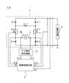
図1は、本発明の第1の実施形態における電源装置10を示す回路構成図である。電源装置10は、力率改善回路1を備え、力率改善回路1の後段に接続される負荷回路2に電力を供給している。力率改善回路1は、交流電源Vacから入力される交流電圧を整流、昇圧、及び力率改善し、負荷回路2に印加する機能を担うものである。負荷回路2は、典型的には、DC−DCコンバータ回路またはDC−ACコンバータ回路から構成され、電源装置10は、その入力段に力率改善回路1を備えたAC−DCコンバータまたはAC−ACコンバータをなす。但し、本発明は、負荷回路2の具体的構成によって限定されるものではなく、任意の適切な回路とすることができる。Hereinafter, embodiments of the present invention will be described with reference to the accompanying drawings.
FIG. 1 is a circuit configuration diagram showing a
力率改善回路1は、第1の整流素子D1と第1のスイッチング素子Q1と第3の整流素子D3からなる第1の直列回路(必要な場合、符号「D1−Q1−D3」を付す)と、第2の整流素子D2と第2のスイッチング素子Q2と第4の整流素子D4からなる第2の直列回路(必要な場合、符号D2−Q2−D4を付す)とを備えている。 The power
力率改善回路1では、第1〜第4の整流素子D1〜D4としてダイオードが用いられ、第1、第2のスイッチング素子Q1、Q2としてMOS−FETが用いられており、第1の直列回路は、第1の整流素子D1のアノード端子と第1のスイッチング素子Q1のドレイン端子とを接続し、さらに、第1のスイッチング素子Q1のソース端子と第3の整流素子D3のカソード端子を接続してなり、第2の直列回路は、第2の整流素子D2のアノード端子と第2のスイッチング素子Q2のドレイン端子とを接続し、さらに、第2のスイッチング素子Q2のソース端子と第4の整流素子D4のカソード端子を接続してなる。 In the power
第1の直列回路と第2の直列回路は、第1、第2の整流素子D1、D2のカソード端子同士を接続し、また、第3、第4の整流素子D3、D4のアノード端子同士を接続して、互いに並列に接続されている。さらに、第1、第2の整流素子D1、D2のカソード端子同士の接続点には、平滑コンデンサC1の一端が接続され、また、第3、第4の整流素子D3、D4のアノード端子同士の接続点には、平滑コンデンサC1の他端が接続されており、このように、平滑コンデンサC1は、第1の直列回路及び第2の直列回路と並列に接続される。そして、平滑コンデンサC1と並列に負荷回路2が接続される。 The first series circuit and the second series circuit connect the cathode terminals of the first and second rectifying elements D1 and D2, and connect the anode terminals of the third and fourth rectifying elements D3 and D4 to each other. Connected and connected in parallel to each other. Furthermore, one end of the smoothing capacitor C1 is connected to the connection point between the cathode terminals of the first and second rectifying elements D1 and D2, and between the anode terminals of the third and fourth rectifying elements D3 and D4. The other end of the smoothing capacitor C1 is connected to the connection point, and thus the smoothing capacitor C1 is connected in parallel with the first series circuit and the second series circuit. The
また、力率改善回路1は、リアクトルL1を備えており、リアクトルL1の一端は、第1の整流素子D1と第1のスイッチング素子Q1の接続点に接続され、他端は、第2の整流素子D2と第2のスイッチング素子Q2の接続点に接続される。電源装置10において、交流電源Vacの一端L(以下、L側の端子ともいう)は、第1のスイッチング素子Q1と第3の整流素子D3との接続点に接続され、他端N(以下、N側の端子ともいう)は、第2のスイッチング素子Q2と第4の整流素子D4との接続点に接続されている。 The power
以上のように構成された電源装置10において、第3、第4の整流素子D3、D4のアノード端子と平滑コンデンサC1の一端の接続ラインが、力率改善回路1の出力電圧のグランドを構成する。 In the
電源装置10は、さらに、第1、第2のスイッチング素子Q1、Q2のスイッチング動作(オン・オフ動作)を制御する駆動制御回路(制御回路部の一例)3を備えている。駆動制御回路3には、力率改善回路1から負荷回路2に出力される出力電圧Voが入力され、この出力電圧Voに応じて第1、第2のスイッチング素子Q1、Q2のスイッチング動作を制御することにより、力率改善回路1の所望の出力電圧を達成する。また、駆動制御回路3には、交流電源Vacの交流電圧が、L側の端子電圧Vi3とN側の端子電圧Vi4として入力されており、これによって、駆動制御回路3は、後述するように第1、第2のスイッチング素子Q1、Q2に対する適正な駆動信号(この場合、ゲート駆動電圧S1、S2)を生成する。 The
ここで、本発明では、交流電源Vacの極性について、交流電源Vacの両端L、NのうちL側の端子電圧がN側の端子電圧よりも高電圧となる半周期間の極性を正極性といい、N側の端子電圧がL側の端子電圧よりも高電圧となる半周期間の極性を負極性というものとする。そして、電源装置10は、交流電源Vacの正負の極性を判別するためのAC極性検出回路4を備えており、AC極性検出回路4には、交流電源Vacの交流電圧が入力され、駆動制御回路3には、交流電源Vacの極性を示すAC極性信号Vi1、Vi2が入力されている。 Here, in the present invention, regarding the polarity of the AC power supply Vac, the polarity during a half cycle in which the terminal voltage on the L side of the both ends L and N of the AC power supply Vac is higher than the terminal voltage on the N side is called positive polarity. The polarity between the half cycles when the terminal voltage on the N side is higher than the terminal voltage on the L side is called negative polarity. The
以上のような構成された電源装置10が備える力率改善回路1は、駆動制御回路3から出力されるスイッチング素子の駆動信号S1、S2に従って、第1、第2のスイッチング素子Q1、Q2をスイッチング動作させることにより、第1、第2のスイッチング素子Q1、Q2を共有するブリッジレス整流回路と昇圧回路とが一体化された力率改善回路として機能するものである。 The power
以下、図1とともに図2〜図4を参照して、電源装置10の第1の制御方法における動作について説明する。尚、第1の制御方法は、以下に説明するように交流電源Vacの全周期にわたって第1のスイッチング素子Q1と第2のスイッチング素子Q2を同期してスイッチング動作させるものであるため、少なくともそのスイッチング動作のために、駆動制御回路3において交流電源Vacの極性の正負を判別する必要はない。したがって、電源装置10を第1の制御方法で動作させる場合には、図1に示す回路構成からAC極性検出回路4を削除することができる。 Hereinafter, the operation in the first control method of the
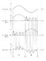
ここで、図2に示す各波形は、(a)が、交流電源Vacの両端間の電圧波形、(b)が、第1のスイッチング素子Q1に対する駆動信号(以下、ゲート駆動電圧ともいう)S1、(c)が、第2のスイッチング素子Q2に対する駆動信号(以下、ゲート駆動電圧ともいう)S2、(d)がリアクトルL1に流れるリアクトル電流IL1である。また、図3(a)は、交流電源Vacが正極性となる半周期間の電流経路W1、W2を示す図、図3(b)は、交流電源Vacが負極性となる半周期間の電流経路W3、W4を示す図である。 Here, in each waveform shown in FIG. 2, (a) is a voltage waveform between both ends of the AC power supply Vac, and (b) is a drive signal (hereinafter also referred to as a gate drive voltage) S1 for the first switching element Q1. , (C) is a drive signal (hereinafter also referred to as a gate drive voltage) S2 for the second switching element Q2, and (d) is a reactor current IL1 flowing through the reactor L1. 3A shows current paths W1 and W2 during a half cycle in which the AC power supply Vac has a positive polarity, and FIG. 3B shows a current path W3 in a half cycle in which the AC power supply Vac has a negative polarity. , W4.
尚、図2において、(a)に示す交流電源Vacの電圧波形は、その中性点を基準(0)として示したものであり、図2(b)、(c)に示すゲート駆動電圧S1、S2は、力率改善回路1の出力電圧のグランドを基準(0)として示された電圧波形である。
また、図2(d)において、リアクトル電流IL1は、第1の整流素子D1と第1のスイッチング素子Q1との接続点側の一端から、第2の整流素子D2と第2のスイッチング素子Q2との接続点側の一端へ向かって流れる方向を正方向として示されている。In FIG. 2, the voltage waveform of the AC power supply Vac shown in FIG. 2A shows the neutral point as a reference (0), and the gate drive voltage S1 shown in FIGS. 2B and 2C. , S2 is a voltage waveform shown with the ground of the output voltage of the power
In FIG. 2D, the reactor current IL1 is generated from one end on the connection point side between the first rectifying element D1 and the first switching element Q1, and the second rectifying element D2 and the second switching element Q2. The direction of flow toward one end of the connection point is indicated as the positive direction.
まず、交流電源Vacが正極性となる半周期では、第1及び第2のスイッチング素子Q1、Q2のゲート駆動電圧S1、S2がハイレベルとなり、これらのスイッチング素子がターンオンされると、交流電源VacのL側の端子から、第1のスイッチング素子Q1のソース−ドレイン間、リアクトルL1、第2のスイッチング素子Q2のソース−ドレイン間を経て、交流電源VacのN側の端子に至る入力電流の電流経路W1(図3(a))が形成され、リアクトルL1に流れる正方向のリアクトル電流IL1が次第に増大するとともに、リアクトルL1にその電流値に応じたエネルギーが蓄積される。 First, in the half cycle in which the AC power supply Vac is positive, the gate drive voltages S1 and S2 of the first and second switching elements Q1 and Q2 are at a high level, and when these switching elements are turned on, the AC power supply Vac is turned on. Current flowing from the L-side terminal of the first switching element Q1 to the N-side terminal of the AC power supply Vac through the reactor L1 and the source-drain of the second switching element Q2 A path W1 (FIG. 3A) is formed, and the positive reactor current IL1 flowing through the reactor L1 gradually increases, and energy corresponding to the current value is accumulated in the reactor L1.
次いで、第1及び第2のスイッチング素子Q1、Q2がターンオフされると、交流電源VacのL側の端子から、第1のスイッチング素子Q1の寄生ダイオード、リアクトルL1、第2の整流素子D2を通じて、平滑コンデンサC1を充電するように入力電流が流れる電流経路W2(図3(a))が形成され、第1及び第2のスイッチング素子Q1、Q2のオン期間にリアクトルL1に蓄積されたエネルギーが平滑コンデンサC1に移送される。この間に、リアクトル電流IL1は、第1及び第2のスイッチング素子Q1、Q2のターンオフ直前の値をピーク値として、次第に減少する。そして、電源装置10において、この電流経路W2の交流電源VacのN側端子へのリターンパスは、第4の整流素子D4を通じて提供される。 Next, when the first and second switching elements Q1, Q2 are turned off, from the L-side terminal of the AC power supply Vac, through the parasitic diode of the first switching element Q1, the reactor L1, the second rectifying element D2, A current path W2 (FIG. 3A) through which an input current flows is formed so as to charge the smoothing capacitor C1, and the energy accumulated in the reactor L1 during the ON period of the first and second switching elements Q1 and Q2 is smoothed. It is transferred to the capacitor C1. During this time, the reactor current IL1 gradually decreases with the value immediately before the turn-off of the first and second switching elements Q1, Q2 as a peak value. In the
次いで、駆動制御回路3は、所定の期間の経過後、再び第1及び第2のスイッチング素子Q1、Q2をターンオンさせ、正の半周期の間、このような第1及び第2のスイッチング素子Q1、Q2の同期したスイッチング動作を繰り返すことになる。この際、典型的には、各スイッチング動作におけるターンオン期間は、駆動制御回路3に入力される出力電圧Vo等に基づいて制御され、これによって、力率改善回路1から所望の直流電圧を負荷回路2に供給する。 Next, the
また、電源装置10では、交流電源Vacの正極性の半周期間、上述した電流経路W1、W2が形成されることにより、交流電源VacのN側の端子は、第4の整流素子D4を通じて力率改善回路1の出力グランドに接地されることになる。したがって、駆動制御回路3に入力される交流電源VacのN側の端子電圧Vi4はグランド電位に保持され、高電圧であるL側の端子電圧Vi3は、力率改善回路1の出力グランドを基準とする交流電源Vacの両端間電圧となる。 Further, in the
そして、電源装置10において、駆動制御回路3は、第1及び第2のスイッチング素子Q1、Q2のゲート駆動電圧S1、S2として、第1及び第2のスイッチング素子Q1、Q2の仕様に基づく所定のゲート−ソース間電圧に対して、それぞれ入力される交流電源Vacの端子電圧Vi3、Vi4を重畳して出力するように構成されている。したがって、交流電源Vacが正極性となる半周期間において、ソース端子が交流電源Vacの高電圧側の端子Lに接続されている第1のスイッチング素子Q1には、所定のゲート−ソース間電圧に対して交流電源Vacの両端間電圧が正電圧として重畳されたゲート駆動電圧S1が出力され、ソース端子が低電圧側の端子Nに接続されている第2のスイッチング素子Q2には、所定のゲート−ソース間電圧がゲート駆動電圧S2としてそのまま出力される。電源装置10では、これによって、第1及び第2のスイッチング素子Q1、Q2の両方に対して、スイッチング動作のために適切なレベルのゲート駆動電圧S1、S2が供給される。 In the
次に、交流電源Vacが負極性となる半周期では、第1及び第2のスイッチング素子Q1、Q2のゲート駆動電圧S1、S2がハイレベルとなり、これらのスイッチング素子がターンオンされると、交流電源VacのN側の端子から、第2のスイッチング素子Q2のソース−ドレイン間、リアクトルL1、第1のスイッチング素子Q1のソース−ドレイン間を経て、交流電源VacのL側の端子に至る入力電流の電流経路W3(図3(b))が形成され、リアクトルL1に流れる負方向のリアクトル電流IL1が次第に増大するとともに、リアクトルL1にその電流値に応じたエネルギーが蓄積される。 Next, in the half cycle in which the AC power supply Vac has a negative polarity, the gate drive voltages S1 and S2 of the first and second switching elements Q1 and Q2 become high level, and when these switching elements are turned on, the AC power supply The input current from the N-side terminal of Vac to the L-side terminal of the AC power supply Vac through the source-drain of the second switching element Q2, the reactor L1, and the source-drain of the first switching element Q1 A current path W3 (FIG. 3B) is formed, and the negative reactor current IL1 flowing through the reactor L1 gradually increases, and energy corresponding to the current value is accumulated in the reactor L1.
次いで、第1及び第2のスイッチング素子Q1、Q2がターンオフされると、交流電源VacのN側の端子から、第2のスイッチング素子Q2の寄生ダイオード、リアクトルL1、第1の整流素子D1を通じて、平滑コンデンサC1を充電するように入力電流が流れる電流経路W4(図3(b))が形成され、第1及び第2のスイッチング素子Q1、Q2のオン期間にリアクトルL1に蓄積されたエネルギーが平滑コンデンサC1に移送される。この間に、リアクトル電流IL1は、第1及び第2のスイッチング素子Q1、Q2のターンオフ直前の値をピーク値として、次第に減少する。そして、電源装置10において、この電流経路W4の交流電源VacのL側端子へのリターンパスは、第3の整流素子D3を通じて提供される。 Next, when the first and second switching elements Q1, Q2 are turned off, from the N-side terminal of the AC power supply Vac, through the parasitic diode of the second switching element Q2, the reactor L1, the first rectifying element D1, A current path W4 (FIG. 3 (b)) through which an input current flows so as to charge the smoothing capacitor C1 is formed, and the energy accumulated in the reactor L1 during the ON period of the first and second switching elements Q1 and Q2 is smoothed. It is transferred to the capacitor C1. During this time, the reactor current IL1 gradually decreases with the value immediately before the turn-off of the first and second switching elements Q1, Q2 as a peak value. And in the
次いで、駆動制御回路3は、所定の期間の経過後、再び第1及び第2のスイッチング素子Q1、Q2をターンオンさせ、負の半周期の間、このような第1及び第2のスイッチング素子Q1、Q2の同期したスイッチング動作を繰り返すことになる。この際、典型的には、各スイッチング動作におけるターンオン期間は、駆動制御回路3に入力される出力電圧Vo等に基づいて制御され、これによって、力率改善回路1から所望の直流電圧を負荷回路2に供給する。 Next, the
また、電源装置10では、交流電源Vacの負極性の半周期間、上述した電流経路W3、W4が形成されることにより、交流電源VacのL側の端子は、第3の整流素子D3を通じて力率改善回路1の出力グランドに接地されることになる。したがって、駆動制御回路3に入力される交流電源VacのL側の端子電圧Vi3はグランド電位に保持され、高電圧であるN側の端子電圧Vi4は、力率改善回路1の出力グランドを基準とする交流電源Vacの両端間電圧となる。 Further, in the
これによって、交流電源Vacが負極性となる半周期間において、ソース端子が交流電源Vacの高電圧側の端子Nに接続されている第2のスイッチング素子Q2には、所定のゲート−ソース間電圧に対して交流電源Vacの両端間電圧が正電圧として重畳されたゲート駆動電圧S2が出力され、ソース端子が低電圧側の端子Lに接続されている第1のスイッチング素子Q1には、所定のゲート−ソース間電圧がゲート駆動電圧S1としてそのまま出力される。これによって、電源装置10では、負の半周期においても、第1及び第2のスイッチング素子Q1、Q2の両方に対して、スイッチング動作のために適切なレベルのゲート駆動電圧S1、S2が供給される。 Accordingly, the second switching element Q2 whose source terminal is connected to the high-voltage side terminal N of the AC power supply Vac has a predetermined gate-source voltage during a half cycle in which the AC power supply Vac has a negative polarity. On the other hand, a gate drive voltage S2 in which the voltage across the AC power supply Vac is superimposed as a positive voltage is output, and the first switching element Q1 whose source terminal is connected to the low-voltage side terminal L has a predetermined gate. -The source-to-source voltage is output as it is as the gate drive voltage S1. Thus, in the
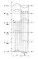
尚、図2(b)〜(d)において、ゲート駆動電圧S1、S2及びリアクトル電流IL1は、動作を分かりやすくすることを目的として、比較的低周波数の波形として模式的に示されている。電源装置10の実際の動作では、図4(a)及びそのA1部分の拡大図(図4(b))及びB1部分の拡大図(図4(c))に、リアクトル電流IL1の電流波形を示すように、ゲート駆動電圧S1、S2のパルス周波数(第1及び第2のスイッチング素Q1、Q2のスイッチング周波数)及びそれに伴うリアクトル電流ILの電流波形の振動周波数は、典型的には、交流電源Vacの交流電圧の周波数に対して、非常に高い周波数を有するものである。なお、本実施例は、臨界モードでの動作例を示したが、これに限定されるものではなく、動作モードは連続モードあるいは不連続モードであってもよい。 2B to 2D, the gate drive voltages S1 and S2 and the reactor current IL1 are schematically shown as relatively low-frequency waveforms for the purpose of making the operation easy to understand. In actual operation of the
このように、電源装置10は、低廉かつ簡素な力率改善回路1を用いて、交流電源Vacから入力される交流電圧を整流、昇圧するとともに、力率改善を実施するものである。その際、電源装置10では、交流電源Vacが力率改善回路1の出力電圧のグランドからフローティングとならない構成としたことにより、従来の電源装置と比較して、EMIノイズを低減することが可能となる。 As described above, the
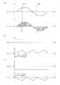
図5に、電源装置のEMIノイズを測定した実測データの一例を示す。図5(a)は、比較例として、従来の電源装置のEMIノイズの実測データ、図5(b)は、本発明の第1の実施形態に係る電源装置10のEMIノイズの実測データである。図5から、広い周波数帯域にわたって、電源装置10のEMIノイズのレベルが低減していることが分かる。 FIG. 5 shows an example of actual measurement data obtained by measuring the EMI noise of the power supply device. FIG. 5A shows EMI noise measurement data of a conventional power supply device as a comparative example, and FIG. 5B shows EMI noise measurement data of the
次に、図1とともに図6を参照して、電源装置10の第2の制御方法における動作について説明する。ここで、図6に示す各波形は、図2と同様に、(a)が、交流電源Vacの両端間の電圧波形、(b)が、第1のスイッチグ素子Q1に対するゲート駆動電圧S1、(c)が、第2のスイッチグ素子Q2に対するゲート駆動電圧S2、(d)がリアクトルL1に流れるリアクトル電流IL1である。 Next, the operation of the
第2の制御方法は、上述した第1の制御方法と比較して、駆動制御回路3が、第1及び第2のスイッチング素子Q1、Q2を、第1及び第2のスイッチング素子Q1、Q2のうち、交流電源Vacの高電圧側の端子に接続している方のスイッチング素子がオン状態を持続し、他方のスイッチング素子がスイッチング動作するように制御する点で相違するものである。 In the second control method, as compared with the first control method described above, the
具体的には、駆動制御回路3は、交流電源Vacが正極性となる半周期間では、交流電源Vacの高電圧側の端子Lに接続されている第1のスイッチング素子Q1に対して、常時、所定のゲート−ソース間電圧に対して交流電源Vacの両端間電圧が正電圧として重畳されたゲート駆動電圧S1を出力することによって、第1のスイッチング素子Q1をオン状態に保持し、一方、第2のスイッチング素子Q2に対しては、図2(c)に示すゲート駆動電圧S2と同様のゲート駆動電圧S2を出力することによって、スイッチング動作させる。 Specifically, the
これによって、第2の制御方法では、第2のスイッチング素子Q2がターンオフされ、リアクトル電流IL1により平滑コンデンサC1が充電される段階においても、図3(a)に示す電流経路W2に相当する電流経路が、第1のスイッチング素子Q1の寄生ダイオードではなく、そのソース−ドレイン間を通じて形成される。 As a result, in the second control method, even when the second switching element Q2 is turned off and the smoothing capacitor C1 is charged by the reactor current IL1, the current path corresponding to the current path W2 shown in FIG. Is formed not between the parasitic diode of the first switching element Q1 but between its source and drain.
同様に、駆動制御回路3は、交流電源Vacが負極性となる半周期間では、交流電源Vacの高電圧側の端子Nに接続されている第2のスイッチング素子Q2に対して、常時、所定のゲート−ソース間電圧に対して交流電源Vacの両端間電圧が正電圧として重畳されたゲート駆動電圧S2を出力することによって、第2のスイッチング素子Q2をオン状態に保持し、一方、第1のスイッチング素子Q1に対しては、図2(b)に示すゲート駆動電圧S1と同様のゲート駆動電圧S1を出力することによって、スイッチング動作させる。 Similarly, the
これによって、第2の制御方法では、第1のスイッチング素子Q1がターンオフされ、リアクトル電流IL1により平滑コンデンサC1が充電される段階においても、図3(b)に示す電流経路W4に相当する電流経路が、第2のスイッチング素子Q2の寄生ダイオードではなく、そのソース−ドレイン間を通じて形成される。 Thus, in the second control method, the current path corresponding to the current path W4 shown in FIG. 3 (b) is obtained even when the first switching element Q1 is turned off and the smoothing capacitor C1 is charged by the reactor current IL1. Is formed not between the parasitic diode of the second switching element Q2 but between its source and drain.
電源装置10を第2の制御方法に従って動作させた場合、第1の制御方法に従って動作させた場合と同等の作用効果を奏することに加えて、電流経路W2、W4において、第1及び第2のスイッチング素子Q1、Q2の寄生ダイオードに電流が流れないため、電力損失を低減して効率を向上させ、かつ、第1及び第2のスイッチング素子Q1、Q2の温度上昇を防ぐことが可能となる。 When the
尚、第2の制御方法では、駆動制御回路3が交流電源Vacの極性の正負を判別可能なことが必須となる。電源装置10において、この判別は、AC極性検出回路4から駆動制御回路3に入力されるAC極性信号Vi1、Vi2に基づいて実施される。例えば、AC極性信号Vi1、Vi2は、交流電源Vacの端子電圧Vi3、Vi4またはこれらの端子電圧Vi3、Vi4を適切な分圧回路により分圧した電圧であってもよい。但し、AC極性検出回路4及びAC極性信号Vi1、Vi2は、駆動制御回路3が交流電源Vacの極性の正負を判別可能な限り、任意の適切な回路及び信号とすることが可能である。例えば、AC極性信号は、交流電源Vacの極性の正及び負に応じてハイレベル及びローレベルとなる1出力の信号であってもよい。 In the second control method, it is essential that the
次に、図7〜図10を参照して、本発明の第2の実施形態における電源装置10a及びその動作について説明する。尚、以下の説明では、上述した第1の実施形における電源装置10と共通の部分に関する説明は適宜省略し、主として電源装置10との相違点について説明する。電源装置10aの構成は、図7に示すように、第1の実施形態における電源装置10に対して、第1の直列回路の構成要素である第3の整流素子D3が第3のスイッチング素子Q3に置き換えられ、第2の直列回路の構成要素である第4の整流素子D4が第4のスイッチング素子Q4に置き換えられた力率改善回路1aを備えるとともに、駆動制御回路3が、第1及び第2のスイッチング素子Q1、Q2とともに、ゲート駆動電圧S3、S4に従って第3、第4のスイッチング素子Q3、Q4のスイッチング動作を制御する点で相違するものである。 Next, with reference to FIGS. 7-10, the power supply device 10a and its operation | movement in the 2nd Embodiment of this invention are demonstrated. In the following description, the description of the parts common to the
電源装置10aにおいて、第3及び第4のスイッチング素子Q3、Q4は、MOS−FETからなり、第1の直列回路の第1のスイッチング素子Q1のソース端子は、第3のスイッチング素子Q3のドレイン端子に接続され、第2の直列回路の第2のスイッチング素子Q2のソース端子は、第4のスイッチング素子Q4のドレイン端子に接続されている。 In the power supply device 10a, the third and fourth switching elements Q3 and Q4 are made of MOS-FETs, and the source terminal of the first switching element Q1 of the first series circuit is the drain terminal of the third switching element Q3. The source terminal of the second switching element Q2 of the second series circuit is connected to the drain terminal of the fourth switching element Q4.
次に、電源装置10aの第3の制御方法における動作について説明する。この第3の制御方法は、第1及び第2のスイッチング素子Q1、Q2のスイッチング動作に関して上述した第1の制御方法と同様の制御方法である。 Next, an operation in the third control method of the power supply device 10a will be described. This third control method is a control method similar to the first control method described above with respect to the switching operations of the first and second switching elements Q1, Q2.
図8には、電源装置10aの第3の制御方法に従った動作における交流電源Vacの両端間の電圧波形(図8(a))、第1のスイッチング素子Q1に対するゲート駆動電圧S1(図8(b))、第2のスイッチング素子Q2に対するゲート駆動電圧S2(図8(c))、第4のスイッチング素子Q4に対するゲート駆動電圧S4(図8(d))、第3のスイッチング素子Q3に対するゲート駆動電圧S3(図8(e))、及び、リアクトルL1に流れるリアクトル電流IL1(図8(f))が示されている。
また、図9(a)は、交流電源Vacが正極性となる半周期間の電流経路W5、W6を示す図、図9(b)は、交流電源Vacが負極性となる半周期間の電流経路W7、W8を示す図である。FIG. 8 shows a voltage waveform between both ends of the AC power supply Vac in the operation according to the third control method of the power supply device 10a (FIG. 8A), a gate drive voltage S1 for the first switching element Q1 (FIG. 8). (B)), a gate drive voltage S2 for the second switching element Q2 (FIG. 8C), a gate drive voltage S4 for the fourth switching element Q4 (FIG. 8D), and a third switching element Q3. The gate drive voltage S3 (FIG. 8 (e)) and the reactor current IL1 (FIG. 8 (f)) flowing through the reactor L1 are shown.
FIG. 9A is a diagram showing current paths W5 and W6 during a half cycle in which the AC power supply Vac is positive. FIG. 9B is a current path W7 during a half cycle in which the AC power supply Vac is negative. , W8.
第3の制御方法は、駆動制御回路3が、第3及び第4のスイッチング素子Q3、Q4を、第3及び第4のスイッチング素子Q3、Q4のうち交流電源Vacの高電圧側の端子に接続している方のスイッチング素子がオフ状態を持続し、他方のスイッチング素子がスイッチング動作するように制御することを特徴とするものである。 In the third control method, the
具体的には、交流電源Vacが正極性となる半周期では、交流電源Vacの高電圧側の端子Lに接続されている第3のスイッチング素子Q3に対するゲート駆動電圧S3はローレベルに保持され(図8(e))、第3のスイッチング素子Q3はオフ状態に維持される。一方、図8(b)、(c)、(d)に示すように、第4のスイッチング素子Q4に対しては、駆動制御回路3から、第1及び第2のスイッチング素子Q1、Q2に対するゲート駆動電圧S1、S2とは相補的なパルス電圧であるゲート駆動電圧S4が出力され、これによって、第4のスイッチング素子Q4は、第1及び第2のスイッチング素子Q1、Q2のスイッチング動作と相補的なスイッチング動作を実行する。 Specifically, in the half cycle in which the AC power supply Vac is positive, the gate drive voltage S3 for the third switching element Q3 connected to the terminal L on the high voltage side of the AC power supply Vac is held at a low level ( FIG. 8 (e)), the third switching element Q3 is maintained in the OFF state. On the other hand, as shown in FIGS. 8B, 8C, and 8D, the gate for the first and second switching elements Q1, Q2 is supplied from the
したがって、第1及び第2のスイッチング素子Q1、Q2のゲート駆動電圧S1、S2がハイレベルとなり、これらのスイッチング素子がターンオンされている間(第3及び第4のスイッチング素子Q3、Q4はターンオフ)には、交流電源VacのL側の端子から、第1のスイッチング素子Q1のソース−ドレイン間、リアクトルL1、第2のスイッチング素子Q2のソース−ドレイン間を経て、交流電源VacのN側の端子に至る入力電流の電流経路W5(図9(a))が形成され、リアクトルL1に流れる正方向のリアクトル電流IL1が次第に増大するとともに、リアクトルL1にその電流値に応じたエネルギーが蓄積される。 Therefore, the gate drive voltages S1 and S2 of the first and second switching elements Q1 and Q2 are at a high level, and these switching elements are turned on (the third and fourth switching elements Q3 and Q4 are turned off). Includes a terminal on the L side of the AC power supply Vac, a source and a drain of the first switching element Q1, a source and a drain of the reactor L1 and the second switching element Q2, and a terminal on the N side of the AC power supply Vac. A current path W5 (FIG. 9A) of the input current leading to is formed, the positive reactor current IL1 flowing in the reactor L1 gradually increases, and energy corresponding to the current value is accumulated in the reactor L1.
次いで、第1及び第2のスイッチング素子Q1、Q2がターンオフされ、かつ、第4のスイッチング素子Q4がターンオンされると、交流電源VacのL側の端子から、第1のスイッチング素子Q1の寄生ダイオード、リアクトルL1、第2の整流素子D2を通じて、平滑コンデンサC1を充電するように入力電流が流れる電流経路W6(図9(a))が形成され、第1及び第2のスイッチング素子Q1、Q2のオン期間にリアクトルL1に蓄積されたエネルギーが平滑コンデンサC1に移送される。この間に、リアクトル電流IL1は、第1及び第2のスイッチング素子Q1、Q2のターンオフ直前の値をピーク値として、次第に減少する。そして、電源装置10aにおいて、この電流経路W6の交流電源VacのN側端子へのリターンパスは、ターンオンされている第4のスイッチング素子Q4のソース−ドレイン間を通じて提供される。 Next, when the first and second switching elements Q1 and Q2 are turned off and the fourth switching element Q4 is turned on, the parasitic diode of the first switching element Q1 is connected to the L-side terminal of the AC power supply Vac. , A current path W6 (FIG. 9 (a)) through which an input current flows so as to charge the smoothing capacitor C1 through the reactor L1 and the second rectifying element D2 is formed, and the first and second switching elements Q1, Q2 The energy accumulated in the reactor L1 during the ON period is transferred to the smoothing capacitor C1. During this time, the reactor current IL1 gradually decreases with the value immediately before the turn-off of the first and second switching elements Q1, Q2 as a peak value. In the power supply device 10a, the return path to the N-side terminal of the AC power supply Vac of the current path W6 is provided through the source and drain of the fourth switching element Q4 that is turned on.
また、交流電源Vacが負極性となる半周期では、交流電源Vacの高電圧側の端子Nに接続されている第4のスイッチング素子Q4に対するゲート駆動電圧S4はローレベルに保持され(図8(d))、第4のスイッチング素子Q4はオフ状態に維持される。一方、図8(b)、(c)、(e)に示すように、第3のスイッチング素子Q3に対しては、駆動制御回路3から、第1及び第2のスイッチング素子Q1、Q2に対するゲート駆動電圧S1、S2とは相補的なパルス電圧であるゲート駆動電圧S3が出力され、これによって、第3のスイッチング素子Q3は、第1及び第2のスイッチング素子Q1、Q2のスイッチング動作と相補的なスイッチング動作を実行する。 Further, in the half cycle in which the AC power supply Vac has a negative polarity, the gate drive voltage S4 for the fourth switching element Q4 connected to the terminal N on the high voltage side of the AC power supply Vac is held at a low level (FIG. 8 ( d)), the fourth switching element Q4 is maintained in the OFF state. On the other hand, as shown in FIGS. 8B, 8C, and 8E, the gate for the first and second switching elements Q1, Q2 is supplied from the
したがって、第1及び第2のスイッチング素子Q1、Q2のゲート駆動電圧S1、S2がハイレベルとなり、これらのスイッチング素子がターンオンされている間(第3及び第4のスイッチング素子Q3、Q4はターンオフ)には、交流電源VacのN側の端子から、第2のスイッチング素子Q2のソース−ドレイン間、リアクトルL1、第1のスイッチング素子Q1のソース−ドレイン間を経て、交流電源VacのL側の端子に至る入力電流の電流経路W7(図9(b))が形成され、リアクトルL1に流れる負方向のリアクトル電流IL1が次第に増大するとともに、リアクトルL1にその電流値に応じたエネルギーが蓄積される。 Therefore, the gate drive voltages S1 and S2 of the first and second switching elements Q1 and Q2 are at a high level, and these switching elements are turned on (the third and fourth switching elements Q3 and Q4 are turned off). The terminal on the L side of the AC power supply Vac passes from the terminal on the N side of the AC power supply Vac to the source and drain of the second switching element Q2, the reactor L1, and the source and drain of the first switching element Q1. A current path W7 (FIG. 9B) of the input current leading to is formed, the negative reactor current IL1 flowing through the reactor L1 gradually increases, and energy corresponding to the current value is accumulated in the reactor L1.
次いで、第1及び第2のスイッチング素子Q1、Q2がターンオフされ、かつ、第3のスイッチング素子Q3がターンオンされると、交流電源VacのN側の端子から、第1のスイッチング素子Q1の寄生ダイオード、リアクトルL1、第1の整流素子D1を通じて、平滑コンデンサC1を充電するように入力電流が流れる電流経路W8(図9(b))が形成され、第1及び第2のスイッチング素子Q1、Q2のオン期間にリアクトルL1に蓄積されたエネルギーが平滑コンデンサC1に移送される。この間に、リアクトル電流IL1は、第1及び第2のスイッチング素子Q1、Q2のターンオフ直前の値をピーク値として、次第に減少する。そして、電源装置10aにおいて、この電流経路W8の交流電源VacのL側端子へのリターンパスは、ターンオンされている第3のスイッチング素子Q3のソース−ドレイン間を通じて提供される。 Next, when the first and second switching elements Q1 and Q2 are turned off and the third switching element Q3 is turned on, a parasitic diode of the first switching element Q1 is connected from the N-side terminal of the AC power supply Vac. A current path W8 (FIG. 9B) through which an input current flows so as to charge the smoothing capacitor C1 through the reactor L1 and the first rectifying element D1 is formed, and the first and second switching elements Q1, Q2 The energy accumulated in the reactor L1 during the ON period is transferred to the smoothing capacitor C1. During this time, the reactor current IL1 gradually decreases with the value immediately before the turn-off of the first and second switching elements Q1, Q2 as a peak value. In the power supply device 10a, a return path to the L-side terminal of the AC power supply Vac of the current path W8 is provided through the source and drain of the third switching element Q3 that is turned on.
以上のように、電源装置10aを第3の制御方法に従って動作させた場合、電源装置10を第1の制御方法に従って動作させた場合と同等の作用効果を奏することに加えて、電流経路W6、W8において、第3及び第4の整流素子D3、D4ではなく、第4及び第3のスイッチング素子Q4、Q3のソース−ドレイン間に電流が流れるため、電力損失を低減して効率を向上させることが可能となる。 As described above, when the power supply device 10a is operated according to the third control method, in addition to the same effects as when the
さらに、本実施形態における電源装置10aは、第4の制御方法に従って動作させるものであってもよい。第4の制御方法は、第1及び第2のスイッチング素子Q1、Q2のスイッチング動作に関して上述した第2の制御方法と同様の制御方法であり、図10には、第4の制御方法に従って電源装置10aを動作させた場合の、図8と同様の波形が示されている。 Furthermore, the power supply apparatus 10a in the present embodiment may be operated according to the fourth control method. The fourth control method is a control method similar to the second control method described above with respect to the switching operation of the first and second switching elements Q1, Q2, and FIG. 10 shows a power supply device according to the fourth control method. A waveform similar to that of FIG. 8 when 10a is operated is shown.
第4の制御方法は、交流電源Vacが正極性となる半周期間では、第1及び第2のスイッチング素子Q1、Q2のうち、第2のスイッチング素子Q2のみがスイッチング動作し(図10(a)、(b))、交流電源Vacが負極性となる半周期間では、第1及び第2のスイッチング素子Q1、Q2のうち、第1のスイッチング素子Q1のみがスイッチング動作する(図10(a)、(b))ことに応じて、交流電源Vacが正極性となる半周期間では、第4のスイッチング素子Q4は第2のスイッチング素子Q2のスイッチング動作と相補的にスイッチング動作し(図10(c)、(d))、交流電源Vacが負極性となる半周期間では、第3のスイッチング素子Q3は第1のスイッチング素子Q1のスイッチング動作と相補的にスイッチング動作する(図10(b)、(e))点を除いて、上述した第3の制御方法と同様のものである。 In the fourth control method, only the second switching element Q2 performs the switching operation among the first and second switching elements Q1 and Q2 during the half cycle in which the AC power supply Vac is positive (FIG. 10A). , (B)) During the half cycle in which the AC power supply Vac has a negative polarity, only the first switching element Q1 performs the switching operation among the first and second switching elements Q1 and Q2 (FIG. 10A, (B)) Accordingly, during the half cycle in which the AC power supply Vac is positive, the fourth switching element Q4 performs a switching operation complementary to the switching operation of the second switching element Q2 (FIG. 10C). , (D)), the third switching element Q3 is switched on in a complementary manner to the switching operation of the first switching element Q1 during a half cycle in which the AC power supply Vac is negative. It operates (FIG. 10 (b), (e)) with the exception of points, is similar to the third control method described above.
電源装置10aを第4の制御方法に従って動作させた場合、第3の制御方法に従って動作させた場合と同等の作用効果を奏することに加えて、電流経路W6、W8において、第1及び第2のスイッチング素子Q1、Q2の寄生ダイオードに電流が流れないため、電力損失を低減して効率を向上させ、かつ、第1及び第2のスイッチング素子Q1、Q2の温度上昇を防ぐことが可能となる。 When the power supply device 10a is operated according to the fourth control method, the same effects as when the power supply device 10a is operated according to the third control method are obtained. In addition, in the current paths W6 and W8, the first and second Since no current flows through the parasitic diodes of the switching elements Q1 and Q2, it is possible to reduce power loss and improve efficiency, and to prevent the temperature of the first and second switching elements Q1 and Q2 from rising.
以上、本発明を好ましい実施形態を用いて説明してきたが、本発明に係る電源装置は、上述した実施形態に限定されるものではない。例えば、第1〜第4のスイッチング素子Q1〜Q4は、MOS―FETに限定されず、例えばIGBT等の任意の適切なスイッチング素子を用いることが可能である。さらに、本発明に係る電源装置において、第1〜第4のスイッチング素子Q1〜Q4として寄生ダイオードを有しないスイッチング素子を用いた場合には、寄生ダイオードに電流を流す替わりに、必要に応じてスイッチング素子をターンオンさせるように制御すればよいことは言うまでもない。 As mentioned above, although this invention has been demonstrated using preferable embodiment, the power supply device which concerns on this invention is not limited to embodiment mentioned above. For example, the first to fourth switching elements Q1 to Q4 are not limited to MOS-FETs, and any appropriate switching element such as an IGBT can be used. Furthermore, in the power supply device according to the present invention, when a switching element having no parasitic diode is used as the first to fourth switching elements Q1 to Q4, switching is performed as necessary instead of passing a current through the parasitic diode. Needless to say, the element may be controlled to be turned on.
1,1a:力率改善回路、2:負荷回路、3:駆動制御回路(制御回路部の一例)、4:AC極性検出回路、C1:平滑コンデンサ、D1:第1の整流素子、D2:第2の整流素子、D3:第3の整流素子、D4:第4の整流素子、L1:リアクトル、Q1:第1のスイッチング素子、Q2:第2のスイッチング素子、Q3:第3のスイッチング素子、Q4:第4のスイッチング素子DESCRIPTION OF
Claims (5)
Translated fromJapanese前記交流電源(Vac)の交流電圧および前記負荷回路に出力される出力電圧を入力するとともに、前記第1及び第2のスイッチング素子(Q1、Q2)あるいは前記第1及び第2のスイッチング素子(Q1、Q2)と前記第3及び第4のスイッチング素子(Q3、Q4)のスイッチング動作を制御する制御回路部と、を備えており、
前記交流電源(Vac)は、その一端が前記第1のスイッチング素子(Q1)と第3の整流素子(D3)あるいは第3のスイッチング素子(Q3)との接続点に接続され、他端が、前記第2のスイッチング素子(Q2)と第4の整流素子(D4)あるいは第4のスイッチング素子(Q4)との接続点に接続されていることを特徴とする電源装置。A first series circuit comprising a first rectifier element (D1), a first switching element (Q1) and a third rectifier element (D3) or a third switching element (Q3); and a second rectifier element (D2), a second switching element (Q2) and a fourth rectifying element (D4) or a fourth switching element (Q4), and a second series circuit connected in parallel to the first series circuit And a smoothing capacitor (C1) connected in parallel to the first and second series circuits and the load circuit, and one end at a connection point of the first rectifier element (D1) and the first switching element (Q1). A power factor correction circuit including a reactor (L1) connected at the other end and connected to a connection point between the second rectifying element (D2) and the second switching element (Q2);
The AC voltage of the AC power source (Vac) and the output voltage output to the load circuit are input, and the first and second switching elements (Q1, Q2) or the first and second switching elements (Q1) are input. Q2) and a control circuit unit for controlling the switching operation of the third and fourth switching elements (Q3, Q4),
One end of the AC power source (Vac) is connected to a connection point between the first switching element (Q1) and the third rectifying element (D3) or the third switching element (Q3), and the other end is A power supply device connected to a connection point between the second switching element (Q2) and the fourth rectifying element (D4) or the fourth switching element (Q4).
Priority Applications (1)
| Application Number | Priority Date | Filing Date | Title |
|---|---|---|---|
| JP2012118597AJP2013247732A (en) | 2012-05-24 | 2012-05-24 | Power-supply device |
Applications Claiming Priority (1)
| Application Number | Priority Date | Filing Date | Title |
|---|---|---|---|
| JP2012118597AJP2013247732A (en) | 2012-05-24 | 2012-05-24 | Power-supply device |
Publications (1)
| Publication Number | Publication Date |
|---|---|
| JP2013247732Atrue JP2013247732A (en) | 2013-12-09 |
Family
ID=49847133
Family Applications (1)
| Application Number | Title | Priority Date | Filing Date |
|---|---|---|---|
| JP2012118597APendingJP2013247732A (en) | 2012-05-24 | 2012-05-24 | Power-supply device |
Country Status (1)
| Country | Link |
|---|---|
| JP (1) | JP2013247732A (en) |
Cited By (2)
| Publication number | Priority date | Publication date | Assignee | Title |
|---|---|---|---|---|
| JP2014011941A (en)* | 2012-07-03 | 2014-01-20 | Minebea Co Ltd | Power supply device |
| JP2014124084A (en)* | 2012-12-20 | 2014-07-03 | Tdk Corp | Power factor improvement circuit |
- 2012
- 2012-05-24JPJP2012118597Apatent/JP2013247732A/enactivePending
Cited By (2)
| Publication number | Priority date | Publication date | Assignee | Title |
|---|---|---|---|---|
| JP2014011941A (en)* | 2012-07-03 | 2014-01-20 | Minebea Co Ltd | Power supply device |
| JP2014124084A (en)* | 2012-12-20 | 2014-07-03 | Tdk Corp | Power factor improvement circuit |
Similar Documents
| Publication | Publication Date | Title |
|---|---|---|
| JP4239111B2 (en) | AC-DC converter | |
| JP6073077B2 (en) | Switching power supply and electronic device equipped with switching power supply | |
| KR101851930B1 (en) | Ac-dc converter | |
| JP2012085465A (en) | Power supply device | |
| US20120014149A1 (en) | Power conversion apparatus and method | |
| JP5427862B2 (en) | Power converter | |
| JP2013021831A (en) | Power factor improvement circuit | |
| JP2014054121A (en) | Switching power supply | |
| JP5849599B2 (en) | Forward type DC-DC converter | |
| JP5858217B2 (en) | AC-AC conversion circuit | |
| JP2011166903A (en) | Switching power supply device | |
| JP6022883B2 (en) | Power supply | |
| JP2010172146A (en) | Switching power supply and power supply control semiconductor integrated circuit | |
| JP2020145842A (en) | Power conversion device | |
| US11258353B2 (en) | Power converter | |
| JP5923961B2 (en) | AC / DC converter | |
| JP2013247732A (en) | Power-supply device | |
| KR101609726B1 (en) | Control circuit of switching rectifier with high power factor | |
| JP5105819B2 (en) | DC-DC converter | |
| JP2013176173A (en) | Power-supply device | |
| JP5151889B2 (en) | Power circuit | |
| JP6575462B2 (en) | Voltage converter | |
| JP4423994B2 (en) | Power factor correction circuit | |
| JP6096133B2 (en) | Load drive device | |
| JP5213940B2 (en) | Inrush current reduction circuit and electrical equipment |