JP2013247278A - Switching circuit - Google Patents
Switching circuitDownload PDFInfo
- Publication number
- JP2013247278A JP2013247278AJP2012120822AJP2012120822AJP2013247278AJP 2013247278 AJP2013247278 AJP 2013247278AJP 2012120822 AJP2012120822 AJP 2012120822AJP 2012120822 AJP2012120822 AJP 2012120822AJP 2013247278 AJP2013247278 AJP 2013247278A
- Authority
- JP
- Japan
- Prior art keywords
- wiring
- switch circuit
- drain
- source
- gate electrode
- Prior art date
- Legal status (The legal status is an assumption and is not a legal conclusion. Google has not performed a legal analysis and makes no representation as to the accuracy of the status listed.)
- Pending
Links
Images


Classifications
- H—ELECTRICITY
- H10—SEMICONDUCTOR DEVICES; ELECTRIC SOLID-STATE DEVICES NOT OTHERWISE PROVIDED FOR
- H10D—INORGANIC ELECTRIC SEMICONDUCTOR DEVICES
- H10D86/00—Integrated devices formed in or on insulating or conducting substrates, e.g. formed in silicon-on-insulator [SOI] substrates or on stainless steel or glass substrates
- H10D86/40—Integrated devices formed in or on insulating or conducting substrates, e.g. formed in silicon-on-insulator [SOI] substrates or on stainless steel or glass substrates characterised by multiple TFTs
- H10D86/60—Integrated devices formed in or on insulating or conducting substrates, e.g. formed in silicon-on-insulator [SOI] substrates or on stainless steel or glass substrates characterised by multiple TFTs wherein the TFTs are in active matrices
- H—ELECTRICITY
- H10—SEMICONDUCTOR DEVICES; ELECTRIC SOLID-STATE DEVICES NOT OTHERWISE PROVIDED FOR
- H10D—INORGANIC ELECTRIC SEMICONDUCTOR DEVICES
- H10D86/00—Integrated devices formed in or on insulating or conducting substrates, e.g. formed in silicon-on-insulator [SOI] substrates or on stainless steel or glass substrates
- H10D86/201—Integrated devices formed in or on insulating or conducting substrates, e.g. formed in silicon-on-insulator [SOI] substrates or on stainless steel or glass substrates the substrates comprising an insulating layer on a semiconductor body, e.g. SOI
- H—ELECTRICITY
- H10—SEMICONDUCTOR DEVICES; ELECTRIC SOLID-STATE DEVICES NOT OTHERWISE PROVIDED FOR
- H10D—INORGANIC ELECTRIC SEMICONDUCTOR DEVICES
- H10D86/00—Integrated devices formed in or on insulating or conducting substrates, e.g. formed in silicon-on-insulator [SOI] substrates or on stainless steel or glass substrates
- H10D86/40—Integrated devices formed in or on insulating or conducting substrates, e.g. formed in silicon-on-insulator [SOI] substrates or on stainless steel or glass substrates characterised by multiple TFTs
- H10D86/441—Interconnections, e.g. scanning lines
- H—ELECTRICITY
- H10—SEMICONDUCTOR DEVICES; ELECTRIC SOLID-STATE DEVICES NOT OTHERWISE PROVIDED FOR
- H10D—INORGANIC ELECTRIC SEMICONDUCTOR DEVICES
- H10D88/00—Three-dimensional [3D] integrated devices
- H—ELECTRICITY
- H10—SEMICONDUCTOR DEVICES; ELECTRIC SOLID-STATE DEVICES NOT OTHERWISE PROVIDED FOR
- H10D—INORGANIC ELECTRIC SEMICONDUCTOR DEVICES
- H10D89/00—Aspects of integrated devices not covered by groups H10D84/00 - H10D88/00
- H10D89/10—Integrated device layouts
- H—ELECTRICITY
- H01—ELECTRIC ELEMENTS
- H01L—SEMICONDUCTOR DEVICES NOT COVERED BY CLASS H10
- H01L2924/00—Indexing scheme for arrangements or methods for connecting or disconnecting semiconductor or solid-state bodies as covered by H01L24/00
- H01L2924/0001—Technical content checked by a classifier
- H01L2924/0002—Not covered by any one of groups H01L24/00, H01L24/00 and H01L2224/00
Landscapes
- Design And Manufacture Of Integrated Circuits (AREA)
- Insulated Gate Type Field-Effect Transistor (AREA)
- Semiconductor Integrated Circuits (AREA)
- Metal-Oxide And Bipolar Metal-Oxide Semiconductor Integrated Circuits (AREA)
- Internal Circuitry In Semiconductor Integrated Circuit Devices (AREA)
- Engineering & Computer Science (AREA)
- General Engineering & Computer Science (AREA)
Abstract
Translated fromJapaneseDescription
Translated fromJapaneseスイッチ回路に関する。 The present invention relates to a switch circuit.
スイッチ回路の性能は、オン抵抗と配線間容量で表現され、このオン抵抗と配線間容量との積が重要な指標となる。 The performance of the switch circuit is expressed by an on-resistance and an inter-wiring capacitance, and the product of the on-resistance and the inter-wiring capacitance is an important index.
例えば、スイッチ回路をMOSFETで構成している場合、そのプロセスでオン抵抗、配線間容量のベース値は決まる。MOSFET上の配線によるオン抵抗および配線間容量の影響も無視できない。特に、配線間容量は、プロセス微細化が進むほど配線が接近するので、増加傾向にある。 For example, in the case where the switch circuit is composed of MOSFETs, the base values of the on-resistance and the inter-wiring capacitance are determined by the process. The influence of on-resistance and inter-wiring capacitance due to wiring on the MOSFET cannot be ignored. In particular, the inter-wiring capacitance tends to increase because the wiring becomes closer as the process becomes finer.
オン抵抗と配線間容量の積をより小さくすることが可能なスイッチ回路を提供する。 Provided is a switch circuit capable of further reducing the product of on-resistance and inter-wiring capacitance.
実施形態に従ったスイッチ回路は、半導体基板を備える。スイッチ回路は、前記半導体基板上にゲート絶縁膜を介して設けられ、第1の方向に延在する第1のゲート電極を備える。スイッチ回路は、前記半導体基板上にゲート絶縁膜を介して設けられ、前記第1の方向に延在する第2のゲート電極を備える。スイッチ回路は、一端が、前記第1ゲート電極および前記第2のゲート電極に第2の方向に隣接する前記半導体基板のソース領域に、接続された第1のビア配線を備える。スイッチ回路は、一端が、前記ソース領域とは反対側で前記第1のゲート電極に前記第2の方向に隣接する前記半導体基板の第1のドレイン領域に、接続された第2のビア配線を備える。スイッチ回路は、一端が、前記ソース領域とは反対側で前記第2のゲート電極に前記第2の方向に隣接する前記半導体基板の第2のドレイン領域に、接続された第3のビア配線を備える。スイッチ回路は、前記半導体基板より上方の第1の配線層に設けられ、前記第1の方向に延在し、前記第1のビア配線の他端に接続された第1の配線を備える。スイッチ回路は、前記第1の配線層に設けられ、前記第2のビア配線の他端に接続され、前記第1の方向に延在する第2の配線を備える。スイッチ回路は、前記第1の配線層に設けられ、前記第3のビア配線の他端に接続され、前記第1の方向に延在する第3の配線を備える。スイッチ回路は、一端が前記第1の配線に接続された第4のビア配線を備える。スイッチ回路は、一端が前記第2の配線に接続された第5のビア配線を備える。スイッチ回路は、一端が前記第3の配線に接続された第6のビア配線を備える。スイッチ回路は、前記第1の配線層より上方の第2の配線層に設けられ、前記第1の方向に延在し、前記第4のビア配線の他端に接続された第4の配線を備える。スイッチ回路は、前記第2の配線層に設けられ、前記第1の方向に延在し、前記第5のビア配線の他端に接続された第5の配線を備える。スイッチ回路は、前記第2の配線層に設けられ、前記第1の方向に延在し、前記第6のビア配線の他端に接続された第6の配線を備える。スイッチ回路は、一端が前記第4の配線に接続された第7のビア配線を備える。スイッチ回路は、一端が前記第5の配線に接続された第8のビア配線を備える。スイッチ回路は、一端が前記第6の配線に接続された第9のビア配線を備える。スイッチ回路は、前記第2の配線層より上方の第3の配線層に設けられ、前記第2の方向に延在し、前記第7のビア配線の他端に接続されたソース配線を備える。スイッチ回路は、前記第3の配線層に設けられ、前記ソース配線に隣接して前記第2の方向に延在し、前記第8のビア配線の他端および前記第9のビア配線の他端に接続されたドレイン配線を備える。 The switch circuit according to the embodiment includes a semiconductor substrate. The switch circuit includes a first gate electrode provided on the semiconductor substrate via a gate insulating film and extending in a first direction. The switch circuit includes a second gate electrode provided on the semiconductor substrate via a gate insulating film and extending in the first direction. The switch circuit includes a first via wiring having one end connected to the source region of the semiconductor substrate adjacent to the first gate electrode and the second gate electrode in the second direction. The switch circuit has a second via line connected to the first drain region of the semiconductor substrate, one end of which is opposite to the source region and adjacent to the first gate electrode in the second direction. Prepare. The switch circuit has a third via line connected to the second drain region of the semiconductor substrate, one end of which is opposite to the source region and adjacent to the second gate electrode in the second direction. Prepare. The switch circuit includes a first wiring that is provided in a first wiring layer above the semiconductor substrate, extends in the first direction, and is connected to the other end of the first via wiring. The switch circuit includes a second wiring provided in the first wiring layer, connected to the other end of the second via wiring, and extending in the first direction. The switch circuit includes a third wiring provided in the first wiring layer, connected to the other end of the third via wiring, and extending in the first direction. The switch circuit includes a fourth via wiring having one end connected to the first wiring. The switch circuit includes a fifth via wiring having one end connected to the second wiring. The switch circuit includes a sixth via wiring having one end connected to the third wiring. The switch circuit is provided in a second wiring layer above the first wiring layer, extends in the first direction, and connects a fourth wiring connected to the other end of the fourth via wiring. Prepare. The switch circuit includes a fifth wiring provided in the second wiring layer, extending in the first direction, and connected to the other end of the fifth via wiring. The switch circuit includes a sixth wiring provided in the second wiring layer, extending in the first direction, and connected to the other end of the sixth via wiring. The switch circuit includes a seventh via wiring having one end connected to the fourth wiring. The switch circuit includes an eighth via wiring having one end connected to the fifth wiring. The switch circuit includes a ninth via wiring having one end connected to the sixth wiring. The switch circuit includes a source wiring provided in a third wiring layer above the second wiring layer, extending in the second direction, and connected to the other end of the seventh via wiring. The switch circuit is provided in the third wiring layer, extends in the second direction adjacent to the source wiring, and has the other end of the eighth via wiring and the other end of the ninth via wiring. And a drain wiring connected to.
前記第4の配線は、前記ドレイン配線に対向する領域には位置しておらず、前記第5および第6の配線は、前記ソース配線に対向する領域には位置していない。 The fourth wiring is not located in a region facing the drain wiring, and the fifth and sixth wirings are not located in a region facing the source wiring.
以下、実施形態について図面に基づいて説明する。 Hereinafter, embodiments will be described with reference to the drawings.
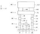
図1は、第1の実施形態に係るスイッチ回路100のレイアウト構成の一例を示す平面図である。また、図2は、図1の第2の方向YのZ1−Z1線に沿った断面の一例を示す断面図である。また、図3は、図1の第2の方向YのZ2−Z2線に沿った断面の一例を示す断面図である。 FIG. 1 is a plan view showing an example of the layout configuration of the
なお、図1において、図2、図3に示すソース領域S、第1、第2のドレイン領域D1、D2、ゲート絶縁膜i、第1ないし第3のビア配線V1〜V3、第1、第2の追加配線AL1、AL2、第10、第11のビア配線AV1、AV2に関しては、簡単のため、図示していない。 In FIG. 1, the source region S, the first and second drain regions D1, D2, the gate insulating film i, the first to third via wirings V1 to V3, the first, the first, and the second regions shown in FIGS. The two additional wirings AL1, AL2, and the tenth and eleventh via wirings AV1, AV2 are not shown for simplicity.
図1ないし図3に示すように、スイッチ回路100は、半導体基板1と、ゲート絶縁膜iと、第1のゲート電極G1と、第2のゲート電極G2と、第1の配線L1と、第2の配線L2と、第3の配線L3と、第4の配線L4と、第5の配線L5と、第6の配線L6と、第7の配線L7と、第8の配線L8と、第9の配線L9と、第1のビア配線V1と、第2のビア配線V2と、第3のビア配線V3と、第4のビア配線V4と、第5のビア配線V5と、第6のビア配線V6と、第7のビア配線V7と、第8のビア配線V8と、第9のビア配線V9と、ソース配線SLと、ドレイン配線DLと、第10のビア配線AV1と、第11のビア配線AV2と、第1の追加配線AL1と、第2の追加配線AL2と、第1の母線BL1と、第2の母線BL2と、を備える。 As shown in FIGS. 1 to 3, the
なお、スイッチ回路100の上記各構成の間は、例えば、層間絶縁膜(図示せず)で満たされている。 In addition, between each said structure of the
半導体基板1は、例えば、SOI基板である。この半導体基板1には、ソース領域Sおよび第1、第2のドレイン領域D1、D2が形成された活性領域AAが形成されている。この活性領域AAは、図示しない素子分離絶縁膜により第1の方向Xと第2の方向Yに区画されている。なお、第1の方向Xと第2の方向Yとは、例えば、略直交している。 The
第1のゲート電極G1は、半導体基板1上にゲート絶縁膜iを介して設けられ、第1の方向Xに延在している。 The first gate electrode G1 is provided on the
第2のゲート電極G2は、半導体基板1上にゲート絶縁膜iを介して設けられ、第1の方向Xに延在している。 The second gate electrode G2 is provided on the
なお、第1のゲート電極G1は、ビア配線VGを介して、ゲート配線LG1に接続されている。また、第2のゲート電極G2は、ビア配線VGを介して、ゲート配線LG2に接続されている。すなわち、第1のゲート電極G1と第2のゲート電極G2とは、電気的に接続されている。 Note that the first gate electrode G1 is connected to the gate wiring LG1 through the via wiring VG. The second gate electrode G2 is connected to the gate wiring LG2 through the via wiring VG. That is, the first gate electrode G1 and the second gate electrode G2 are electrically connected.
また、第1のビア配線V1は、下部(一端)が、第2の方向Yにおいて第1ゲート電極G1および第2のゲート電極G2に隣接する半導体基板1のソース領域Sに接続されている。 The lower portion (one end) of the first via wiring V1 is connected to the source region S of the
第2のビア配線V2は、下部(一端)が、第2の方向Yにおいて第1のゲート電極G1に対してソース領域Sとは反対側に隣接する半導体基板1の第1のドレイン領域D1に接続されている。 The second via wiring V2 has a lower portion (one end) in the first drain region D1 of the
第3のビア配線V3は、下部(一端)が、第2の方向Yにおいて第2のゲート電極G2に対してソース領域Sとは反対側に隣接する半導体基板1の第2のドレイン領域D2に接続されている。 The third via wiring V3 has a lower portion (one end) in the second drain region D2 of the
なお、例えば、半導体基板1と、ソース領域Sと、第1のドレイン領域D1と、ゲート絶縁膜iと、第1のゲート電極G1は、MOSFETを構成する。 For example, the
同様に、例えば、半導体基板1と、ソース領域Sと、第2のドレイン領域D2と、ゲート絶縁膜iと、第2のゲート電極G2は、MOSFETを構成する。 Similarly, for example, the
したがって、第1の方向Xは、MOSFETのチャネル幅方向に対応し、第2の方向Yは、MOSFETのチャネル長方向に対応する。 Therefore, the first direction X corresponds to the channel width direction of the MOSFET, and the second direction Y corresponds to the channel length direction of the MOSFET.
また、第1の配線L1は、半導体基板1より上方の第1の配線層M1に設けられ、第1の方向Xに延在し、下面が第1のビア配線V1の上部(他端)に接続されている。 The first wiring L1 is provided in the first wiring layer M1 above the
第2の配線L2は、第1の配線層M1に設けられ、下面が第2のビア配線V2の上部(他端)に接続され、第1の方向Xに延在している。 The second wiring L2 is provided in the first wiring layer M1, and the lower surface is connected to the upper part (the other end) of the second via wiring V2, and extends in the first direction X.
第3の配線L3は、第1の配線層M1に設けられ、下面が第3のビア配線V3の上部(他端)に接続され、第1の方向Xに延在している。 The third wiring L3 is provided in the first wiring layer M1, the lower surface is connected to the upper part (the other end) of the third via wiring V3, and extends in the first direction X.
また、第4のビア配線V4は、下部(一端)が第1の配線L1の上面に接続されている。 The lower part (one end) of the fourth via wiring V4 is connected to the upper surface of the first wiring L1.
第5のビア配線V5は、下部(一端)が第2の配線L2の上面に接続されている。 The lower portion (one end) of the fifth via wiring V5 is connected to the upper surface of the second wiring L2.
第6のビア配線V6は、下部(一端)が第3の配線L3の上面に接続されている。 The lower portion (one end) of the sixth via wiring V6 is connected to the upper surface of the third wiring L3.
また、第4の配線L4は、第1の配線層M1より上方の第2の配線層M2に設けられ、第1の方向Xに延在し、下面が第4のビア配線V4の上部(他端)に接続されている。 The fourth wiring L4 is provided in the second wiring layer M2 above the first wiring layer M1, extends in the first direction X, and has a lower surface above the fourth via wiring V4 (others). End).
第5の配線L5は、第2の配線層M2に設けられ、第1の方向Xに延在し、下面が第5のビア配線V5の上部(他端)に接続されている。 The fifth wiring L5 is provided in the second wiring layer M2, extends in the first direction X, and its lower surface is connected to the upper part (the other end) of the fifth via wiring V5.
第6の配線L6は、第2の配線層M2に設けられ、第1の方向Xに延在し、下面が第6のビア配線V6の上部(他端)に接続されている。 The sixth wiring L6 is provided in the second wiring layer M2, extends in the first direction X, and its lower surface is connected to the upper part (the other end) of the sixth via wiring V6.
なお、第1ないし第6の配線L1〜L6は、例えば、金属配線である。 Note that the first to sixth wirings L1 to L6 are, for example, metal wirings.
また、第7のビア配線V7は、下部(一端)が第4の配線L4の上面に接続されている。 The seventh via wiring V7 has a lower portion (one end) connected to the upper surface of the fourth wiring L4.
第8のビア配線V8は、下部(一端)が第5の配線L5の上面に接続されている。 The eighth via wiring V8 has a lower portion (one end) connected to the upper surface of the fifth wiring L5.
第9のビア配線V9は、下部(一端)が第6の配線L6の上面に接続されている。 The lower portion (one end) of the ninth via wiring V9 is connected to the upper surface of the sixth wiring L6.
また、ソース配線SLは、第2の配線層M2より上方の第3の配線層M3に設けられ、第2の方向Yに延在し、下面が第7のビア配線V7の上部(他端)に接続されている(図1、図3)。 The source wiring SL is provided in the third wiring layer M3 above the second wiring layer M2, extends in the second direction Y, and the lower surface is the upper part (the other end) of the seventh via wiring V7. (FIGS. 1 and 3).
ドレイン配線DLは、第3の配線層M3に設けられ、ソース配線SLに隣接して第2の方向Yに延在し、下面が第8のビア配線V8の上部(他端)および第9のビア配線V9の上部(他端)に接続されている(図1、図2)。 The drain wiring DL is provided in the third wiring layer M3, extends in the second direction Y adjacent to the source wiring SL, and has a lower surface above the eighth via wiring V8 (the other end) and the ninth. It is connected to the upper part (the other end) of the via wiring V9 (FIGS. 1 and 2).
なお、ソース配線SL、ドレイン配線DLは、例えば、金属配線である。 The source line SL and the drain line DL are, for example, metal lines.
また、例えば、図1に示すように、活性領域AAの中央付近で隣接するソース配線SLとドレイン配線DLとに関して、ソース配線SLの第1の方向Xの幅は、ドレイン配線DLの第1の方向Xの幅と等しい。 For example, as shown in FIG. 1, the width of the source line SL in the first direction X with respect to the adjacent source line SL and drain line DL near the center of the active region AA is the first level of the drain line DL. Equal to width in direction X
さらに、例えば、図1に示すように、ソース配線SLが半導体基板1のソース領域Sおよび第1、第2のドレイン領域D1、D2が形成された活性領域AAの端部に近接する場合(図1の上側のソース配線SLとドレイン配線DLの組み合わせの場合)、ソース配線SLの第1の方向Xの幅は、ドレイン配線DLの第1の方向Xの幅の半分である。 Further, for example, as shown in FIG. 1, when the source wiring SL is close to the end of the active region AA where the source region S of the
同様に、ドレイン配線DLが半導体基板1のソース領域Sおよび第1、第2のドレイン領域D1、D2が形成された活性領域AAの端部に近接する場合(図1の下側のソース配線SLとドレイン配線DLの組み合わせの場合)、ドレイン配線DLの第1の方向Xの幅は、ソース配線SLの第1の方向Xの幅の半分である。 Similarly, when the drain wiring DL is close to the end of the source region S of the
これらのようにしてソース配線SLとドレイン配線DLの幅を規定することにより、これらのソース配線SLとドレイン配線DLに接続されたMOSFETの構成のバランスが均一になる。すなわち、各MOSFETの特性が等しくなる。 By defining the widths of the source wiring SL and the drain wiring DL as described above, the balance of the configuration of the MOSFETs connected to the source wiring SL and the drain wiring DL becomes uniform. That is, the characteristics of the MOSFETs are equal.
これにより、例えば、各第1のゲート電極G1に均一に電流が流れるので、MOSトランジスタのオン抵抗を下げることができる。すなわち、スイッチ回路100のスイッチ性能を向上することができる。 Thereby, for example, since the current flows uniformly to each first gate electrode G1, the on-resistance of the MOS transistor can be lowered. That is, the switch performance of the
さらに、各配線層に流れる電流の粗密が均一化されるので、スイッチ回路100に入力可能な電流、電力をより大きくすることができる。 Furthermore, since the density of the current flowing through each wiring layer is made uniform, the current and power that can be input to the
また、第4の配線L4は、ドレイン配線DLの下方の領域(ドレイン配線DLに対向する領域)には位置していない(図1、図2)。 The fourth wiring L4 is not located in a region below the drain wiring DL (a region facing the drain wiring DL) (FIGS. 1 and 2).
特に、第4の配線L4は、例えば、図1、図3に示すように、ソース配線SLの下方の領域(ソース配線SLに対向する領域)にのみ位置している。 In particular, the fourth wiring L4 is located only in a region below the source wiring SL (a region facing the source wiring SL), for example, as shown in FIGS.
この第4の配線L4の第1の方向Xの長さは、例えば、図1に示すように、ソース配線SLの第1の方向Xの幅と等しい。 The length of the fourth wiring L4 in the first direction X is equal to the width of the source wiring SL in the first direction X, for example, as shown in FIG.
さらに、第5および第6の配線L5、L6は、ソース配線SLの下方の領域(ソース配線SLに対向する領域)には位置していない(図1、図3)。 Further, the fifth and sixth wirings L5 and L6 are not located in a region below the source wiring SL (a region facing the source wiring SL) (FIGS. 1 and 3).
特に、第5および第6の配線L5、L6は、例えば、図1、図2に示すように、ドレイン配線DLの下方の領域(ドレイン配線DLに対向する領域)にのみ位置している。 In particular, the fifth and sixth wirings L5 and L6 are located only in a region below the drain wiring DL (a region facing the drain wiring DL), for example, as shown in FIGS.
この第5および第6の配線L5、L6の第1の方向Xの長さは、例えば、図1に示すように、ドレイン配線DLの第1の方向Xの幅と等しい。 The lengths of the fifth and sixth wirings L5 and L6 in the first direction X are equal to the width of the drain wiring DL in the first direction X, for example, as shown in FIG.
また、第1の母線BL1は、第3の配線層M3に設けられ、第1の方向Xに延在し、ソース配線SLの一端に接続されている。 The first bus line BL1 is provided in the third wiring layer M3, extends in the first direction X, and is connected to one end of the source line SL.
第2の母線BL2は、第1の母線BL2との間に、ソース配線SL、およびドレイン配線DLが位置するように第3の配線層M3に設けられている。この第2の母線BL2は、第1の方向Xに延在し、ドレイン配線DLの一端に接続されている。 The second bus line BL2 is provided in the third wiring layer M3 so that the source line SL and the drain line DL are located between the second bus line BL2 and the first bus line BL2. The second bus line BL2 extends in the first direction X and is connected to one end of the drain wiring DL.
なお、第1、第2の母線BL1、BL2は、例えば、金属配線である。 The first and second buses BL1 and BL2 are, for example, metal wirings.
また、第10のビア配線AV1は、例えば、図3に示すように、下部(一端)がソース配線SLの上面に接続されている。 For example, as shown in FIG. 3, the lower portion (one end) of the tenth via wiring AV1 is connected to the upper surface of the source wiring SL.
また、第11のビア配線AV2は、例えば、図2に示すように、下部(一端)がドレイン配線DLの上面に接続されている。 For example, as shown in FIG. 2, the eleventh via wiring AV2 has a lower portion (one end) connected to the upper surface of the drain wiring DL.
また、図3に示すように、第1の追加配線AL1は、第3の配線層M3より上方の第4の配線層M4に設けられ、下面が第10のビア配線AV1の上部(他端)に接続されている。 Further, as shown in FIG. 3, the first additional wiring AL1 is provided in the fourth wiring layer M4 above the third wiring layer M3, and the lower surface is the upper part (the other end) of the tenth via wiring AV1. It is connected to the.
この第1の追加配線AL1は、例えば、ソース配線SLと同じ平面形状を有する。 For example, the first additional wiring AL1 has the same planar shape as the source wiring SL.
また、図2に示すように、第2の追加配線AL2は、第4の配線層M4に設けられ、第2の方向Yにおいて第1の追加配線AL1に隣接して延在し、下面が第11のビア配線AV2に接続されている。 Further, as shown in FIG. 2, the second additional wiring AL2 is provided in the fourth wiring layer M4, extends adjacent to the first additional wiring AL1 in the second direction Y, and the lower surface is the first. 11 via wiring AV2.
なお、第1、第2の追加配線AL1、AL2は、例えば、金属配線である。 The first and second additional wirings AL1 and AL2 are, for example, metal wirings.
これらの第1、第2の追加配線AL1、AL2により、スイッチ回路100のオン抵抗を低減することができる。 The on-resistance of the
この第2の追加配線AL2は、例えば、ドレイン配線DLと同じ平面形状を有する。 For example, the second additional wiring AL2 has the same planar shape as the drain wiring DL.
特に、図1に示すように、第1ないし第9のビア配線V1〜V9、第4ないし第6の配線L4〜L6、ソース配線SL、および、ドレイン配線DLを含む単位が、第1の方向Xに複数個(図1の例では2個)並んで配置されている。 In particular, as shown in FIG. 1, the unit including the first to ninth via wirings V1 to V9, the fourth to sixth wirings L4 to L6, the source wiring SL, and the drain wiring DL is in the first direction. A plurality (two in the example of FIG. 1) of X are arranged side by side.
これにより、第1の配線層M1にかかる電流負荷を低減することができる。 Thereby, the current load applied to the first wiring layer M1 can be reduced.
したがって、既述のように、第2の配線層M2の第4ないし第6の配線L4〜L6は、櫛形構造にする必要がなく、必要部分のみに配置される。 Therefore, as described above, the fourth to sixth wirings L4 to L6 of the second wiring layer M2 do not need to have a comb structure, and are arranged only in necessary portions.
すなわち、第2の配線層M2の配線間隔が大きくなるので、配線間容量が大幅に低減される。さらに、第3の配線層M3の配線の幅を調整することにより、オン抵抗の低減も可能となる。 That is, since the wiring interval of the second wiring layer M2 is increased, the inter-wiring capacitance is greatly reduced. Furthermore, the on-resistance can be reduced by adjusting the wiring width of the third wiring layer M3.
以上のように、本実施形態に係るスイッチ回路によれば、オン抵抗と配線間容量の積をより小さくすることができる。 As described above, according to the switch circuit according to the present embodiment, the product of the on-resistance and the inter-wiring capacitance can be further reduced.
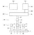
既述の第1の実施形態では、ソース配線(ドレイン配線)と第1の追加配線(第2の追加配線)とが平行である構成の一例について説明した。 In the above-described first embodiment, the example of the configuration in which the source wiring (drain wiring) and the first additional wiring (second additional wiring) are parallel to each other has been described.
本第2の実施形態では、ソース配線(ドレイン配線)と第1の追加配線(第2の追加配線)とが直交する構成の一例について説明する。 In the second embodiment, an example of a configuration in which a source wiring (drain wiring) and a first additional wiring (second additional wiring) are orthogonal to each other will be described.
図4は、第2の実施形態に係るスイッチ回路200のレイアウト構成の一例を示す平面図である。また、図5は、図4の第2の方向YのZ1−Z1線に沿った断面の一例を示す断面図である。また、図6は、図4の第2の方向YのZ2−Z2線に沿った断面の一例を示す断面図である。 FIG. 4 is a plan view showing an example of the layout configuration of the
なお、図4ないし図6において、図1ないし図3の符号と同じ符号は、第1の実施形態と同様の構成を示す。また、図4において、図5、図6に示すソース領域S、第1、第2のドレイン領域D1、D2、ゲート絶縁膜i、第1ないし第3のビア配線V1〜V3に関しては、簡単のため、図示していない。 4 to 6, the same reference numerals as those in FIGS. 1 to 3 indicate the same configurations as those in the first embodiment. 4, the source region S, the first and second drain regions D1 and D2, the gate insulating film i, and the first to third via wirings V1 to V3 shown in FIGS. Therefore, it is not illustrated.
図4ないし図6に示すように、スイッチ回路200は、第1の実施形態のスイッチ回路100と比較して、第1の追加母線BAL1と、第2の追加母線BAL2と、をさらに備える。 As shown in FIGS. 4 to 6, the
第1の追加母線BAL1は、第4の配線層M4に設けられ、第2の方向Yに延在している。そして、各第1の追加配線AL1は、この第1の追加母線BAL1に接続されている。 The first additional bus BAL1 is provided in the fourth wiring layer M4 and extends in the second direction Y. Each first additional wiring AL1 is connected to the first additional bus BAL1.
第2の追加母線BAL2は、第4の配線層M4に設けられ、第2の方向Yに延在している。そして、各第2の追加配線AL2は、この第2の追加母線BAL2に接続されている。 The second additional bus BAL2 is provided in the fourth wiring layer M4 and extends in the second direction Y. Each second additional wiring AL2 is connected to the second additional bus BAL2.
このスイッチ回路200において、各第1および第2の追加配線AL1、AL2は、第1の方向Xに延在している。 In the
すなわち、第4の配線層M4の配線は、櫛形の構成を有する。そして、ソース配線SL(ドレイン配線DL)と第1の追加配線AL1(第2の追加配線AL2)とが直交している。 That is, the wiring of the fourth wiring layer M4 has a comb-like configuration. The source line SL (drain line DL) and the first additional line AL1 (second additional line AL2) are orthogonal to each other.
本実施形態において、多層配線プロセスであれば、適宜櫛型の配線間を空けた状態で上に積み重ねることで、オン抵抗と配線間容量の積を最少化することができる。 In the present embodiment, in the case of a multilayer wiring process, the product of the on-resistance and the capacitance between wirings can be minimized by stacking the wirings with the comb-shaped wirings being appropriately spaced.
スイッチ回路200のその他の構成・機能は、第1の実施形態のスイッチ回路100と同様である。 Other configurations and functions of the
すなわち、本実施形態に係るスイッチ回路によれば、第1の実施形態と同様に、オン抵抗と配線間容量の積をより小さくすることができる。 That is, according to the switch circuit according to the present embodiment, as in the first embodiment, the product of the on-resistance and the inter-wiring capacitance can be further reduced.
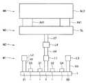
この第3の実施形態では、MOSFETがダブルゲート構造を有する構成の一例について説明する。 In the third embodiment, an example of a configuration in which a MOSFET has a double gate structure will be described.
図7は、第3の実施形態に係るスイッチ回路300のレイアウト構成の一例を示す平面図である。また、図8は、図7の第2の方向YのZ1−Z1線に沿った断面の一例を示す断面図である。また、図9は、図7の第2の方向YのZ2−Z2線に沿った断面の一例を示す断面図である。 FIG. 7 is a plan view illustrating an example of a layout configuration of the
なお、図7ないし図9において、図1ないし図3の符号と同じ符号は、第1の実施形態と同様の構成を示す。また、図7において、図8、図9に示すソース領域S、第1、第2のドレイン領域D1、D2、ゲート絶縁膜i、第1ないし第3のビア配線V1〜V3、第1、第2の追加配線AL1、AL2、第10、第11のビア配線AV1、AV2に関しては、簡単のため、図示していない。 7 to 9, the same reference numerals as those in FIGS. 1 to 3 indicate the same configurations as those in the first embodiment. In FIG. 7, the source region S, the first and second drain regions D1, D2, the gate insulating film i, the first to third via wirings V1 to V3, the first, the first, and the second regions shown in FIGS. The two additional wirings AL1, AL2, and the tenth and eleventh via wirings AV1, AV2 are not shown for simplicity.
図7ないし図9に示すように、このスイッチ回路300は、第1の実施形態のスイッチ回路100と比較して、第3のゲート電極G3と、第4のゲート電極G4と、ゲート配線LG2と、配線Lxと、ビア配線Vxと、をさらに備える。 As shown in FIGS. 7 to 9, the
第3のゲート電極G3は、半導体基板1上にゲート絶縁膜iを介して設けられ、第1の方向Xに延在し、第2の方向Yにおいてソース領域Sと第1のドレイン領域D1との間で第1のゲート電極G1に隣接する。 The third gate electrode G3 is provided on the
第4のゲート電極G4は、半導体基板1上にゲート絶縁膜iを介して設けられ、第1の方向Xに延在し、第2の方向Yにおいてソース領域Sと第2のドレイン領域D2との間で第2のゲート電極G2に隣接する第1の方向Xに延在する。 The fourth gate electrode G4 is provided on the
なお、第3のゲート電極G3は、ビア配線VGを介して、ゲート配線LG2に接続されている。また、第4のゲート電極G4は、ビア配線VGを介して、ゲート配線LG2に接続されている。すなわち、第3のゲート電極G3と第4のゲート電極G4とは、電気的に接続されている。 Note that the third gate electrode G3 is connected to the gate wiring LG2 via the via wiring VG. The fourth gate electrode G4 is connected to the gate wiring LG2 via the via wiring VG. That is, the third gate electrode G3 and the fourth gate electrode G4 are electrically connected.
このように、ダブルゲート化されたスイッチ回路300においても、第1の実施形態と同様の多重化により、配線間容量の低減ができる。 As described above, even in the double
なお、半導体基板1がSOI基板の場合、図7に示すように、配線Lxがビア配線Vxを介して半導体基板1の活性領域AAに電気的に接続される。この配線Lxには、所定の電圧が印加され、または、電圧が出力される。 When the
このスイッチ回路300のその他の構成・機能は、第1の実施形態のスイッチ回路1と同様である。 Other configurations and functions of the
すなわち、本実施形態に係るスイッチ回路によれば、第1の実施形態と同様に、オン抵抗と配線間容量の積をより小さくすることができる。 That is, according to the switch circuit according to the present embodiment, as in the first embodiment, the product of the on-resistance and the inter-wiring capacitance can be further reduced.
なお、実施形態は例示であり、発明の範囲はそれらに限定されない。 In addition, embodiment is an illustration and the range of invention is not limited to them.
100、200、300 スイッチ回路
G1、G2 第1、第2のゲート電極
L1〜L9 第1ないし第9の配線
V1〜V9 第1〜第9のビア配線
SL ソース配線
DL ドレイン配線
AV1、AV2 第10、第11のビア配線
AL1、AL2 第1、第2の追加配線
BL1、BL2 第1、第2の母線100, 200, 300 switch circuit
G1, G2 first and second gate electrodes
L1 to L9 1st to 9th wiring
V1 to V9 1st to 9th via wiring
SL source wiring
DL drain wiring
AV1, AV2 10th and 11th via wirings
AL1, AL2 1st and 2nd additional wiring
BL1, BL2 First and second busbars
Claims (17)
Translated fromJapanese前記半導体基板にゲート絶縁膜を介して設けられ、第1の方向に延在する第1のゲート電極と、
前記半導体基板にゲート絶縁膜を介して設けられ、前記第1の方向に延在する第2のゲート電極と、
一端が、第2の方向において前記第1ゲート電極および前記第2のゲート電極に隣接するソース領域に接続された第1のビア配線と、
一端が、前記第1のゲート電極に対して前記ソース領域とは反対側に隣接する第1のドレイン領域に接続された第2のビア配線と、
一端が、前記第2のゲート電極に対して前記ソース領域とは反対側に隣接する第2のドレイン領域に接続された第3のビア配線と、
第1の配線層に設けられ、前記第1の方向に延在し、前記第1のビア配線の他端に接続された第1の配線と、
前記第1の配線層に設けられ、前記第2のビア配線の他端に接続され、前記第1の方向に延在する第2の配線と、
前記第1の配線層に設けられ、前記第3のビア配線の他端に接続され、前記第1の方向に延在する第3の配線と、
一端が前記第1の配線に接続された第4のビア配線と、
一端が前記第2の配線に接続された第5のビア配線と、
一端が前記第3の配線に接続された第6のビア配線と、
第2の配線層に設けられ、前記第1の方向に延在し、前記第4のビア配線の他端に接続された第4の配線と、
前記第2の配線層に設けられ、前記第1の方向に延在し、前記第5のビア配線の他端に接続された第5の配線と、
前記第2の配線層に設けられ、前記第1の方向に延在し、前記第6のビア配線の他端に接続された第6の配線と、
一端が前記第4の配線に接続された第7のビア配線と、
一端が前記第5の配線に接続された第8のビア配線と、
一端が前記第6の配線に接続された第9のビア配線と、
第3の配線層に設けられ、前記第2の方向に延在し、前記第7のビア配線の他端に接続されたソース配線と、
前記第3の配線層に設けられ、前記ソース配線に隣接して前記第2の方向に延在し、前記第8のビア配線の他端および前記第9のビア配線の他端に接続されたドレイン配線と、を備え、
前記第4の配線は、前記ドレイン配線に対向する領域には位置しておらず、
前記第5および第6の配線は、前記ソース配線に対向する領域には位置していないことを特徴とするスイッチ回路。A semiconductor substrate;
A first gate electrode provided on the semiconductor substrate via a gate insulating film and extending in a first direction;
A second gate electrode provided on the semiconductor substrate via a gate insulating film and extending in the first direction;
A first via wiring having one end connected to the source region adjacent to the first gate electrode and the second gate electrode in a second direction;
A second via wiring having one end connected to the first drain region adjacent to the first gate electrode on the opposite side of the source region;
A third via wiring having one end connected to a second drain region adjacent to the second gate electrode on the opposite side of the source region;
A first wiring provided in a first wiring layer, extending in the first direction and connected to the other end of the first via wiring;
A second wiring provided in the first wiring layer, connected to the other end of the second via wiring, and extending in the first direction;
A third wiring provided in the first wiring layer, connected to the other end of the third via wiring, and extending in the first direction;
A fourth via wiring having one end connected to the first wiring;
A fifth via wiring having one end connected to the second wiring;
A sixth via wiring having one end connected to the third wiring;
A fourth wiring provided in the second wiring layer, extending in the first direction and connected to the other end of the fourth via wiring;
A fifth wiring provided in the second wiring layer, extending in the first direction and connected to the other end of the fifth via wiring;
A sixth wiring provided in the second wiring layer, extending in the first direction and connected to the other end of the sixth via wiring;
A seventh via wiring having one end connected to the fourth wiring;
An eighth via wiring having one end connected to the fifth wiring;
A ninth via wiring having one end connected to the sixth wiring;
A source wiring provided in a third wiring layer, extending in the second direction and connected to the other end of the seventh via wiring;
Provided in the third wiring layer, extending in the second direction adjacent to the source wiring, and connected to the other end of the eighth via wiring and the other end of the ninth via wiring; Drain wiring, and
The fourth wiring is not located in a region facing the drain wiring,
The switch circuit, wherein the fifth and sixth wirings are not located in a region facing the source wiring.
前記第5および第6の配線は、前記ドレイン配線に対向する領域にのみ位置していることを特徴とする請求項1または2に記載のスイッチ回路。The fourth wiring is located only in a region facing the source wiring,
3. The switch circuit according to claim 1, wherein the fifth and sixth wirings are located only in a region facing the drain wiring. 4.
前記第5および第6の配線の前記第1の方向の長さは、前記ドレイン配線の前記第1の方向の幅と等しいことを特徴とする請求項3に記載のスイッチ回路。The length of the fourth wiring in the first direction is equal to the width of the source wiring in the first direction,
4. The switch circuit according to claim 3, wherein a length of the fifth and sixth wirings in the first direction is equal to a width of the drain wiring in the first direction.
一端が前記ドレイン配線に接続された第11のビア配線と、
第4の配線層に設けられ、前記第10のビア配線の他端に接続された第1の追加配線と、
前記第4の配線層に設けられ、前記第2の方向において前記第1の追加配線に隣接して延在し、前記第11のビア配線に接続された第2の追加配線と、をさらに備えることを特徴とする請求項1に記載のスイッチ回路。A tenth via wiring having one end connected to the source wiring;
An eleventh via wiring having one end connected to the drain wiring;
A first additional wiring provided in a fourth wiring layer and connected to the other end of the tenth via wiring;
A second additional wiring provided in the fourth wiring layer, extending adjacent to the first additional wiring in the second direction and connected to the eleventh via wiring; The switch circuit according to claim 1.
前記第2の追加配線は、前記ドレイン配線と同じ平面形状を有することを特徴とする請求項8に記載のスイッチ回路。The first additional wiring has the same planar shape as the source wiring,
The switch circuit according to claim 8, wherein the second additional wiring has the same planar shape as the drain wiring.
前記半導体基板にゲート絶縁膜を介して設けられ、前記第1の方向に延在し、前記第2の方向において前記ソース領域と前記第2のドレイン領域との間で前記第2のゲート電極に隣接する前記第1の方向に延在する第4のゲート電極と、をさらに備えることを特徴とする請求項1に記載のスイッチ回路。The semiconductor substrate is provided with a gate insulating film interposed therebetween, extends in the first direction, and extends between the source region and the first drain region in the second direction. An adjacent third gate electrode;
The semiconductor substrate is provided with a gate insulating film interposed therebetween, extends in the first direction, and extends between the source region and the second drain region in the second direction. The switch circuit according to claim 1, further comprising: a fourth gate electrode extending in the adjacent first direction.
前記第1の母線との間に前記ソース配線および前記ドレイン配線が位置するように前記第3の配線層に設けられ、前記第1の方向に延在し、前記ドレイン配線の一端に接続された第2の母線と、をさらに備えることを特徴とする請求項13に記載のスイッチ回路。A first bus provided in the third wiring layer, extending in the first direction and connected to one end of the source wiring;
Provided in the third wiring layer so that the source wiring and the drain wiring are located between the first bus and the first bus, extend in the first direction, and connected to one end of the drain wiring The switch circuit according to claim 13, further comprising a second busbar.
Priority Applications (3)
| Application Number | Priority Date | Filing Date | Title |
|---|---|---|---|
| JP2012120822AJP2013247278A (en) | 2012-05-28 | 2012-05-28 | Switching circuit |
| CN201310051656.1ACN103456713B (en) | 2012-05-28 | 2013-02-16 | Switching circuit |
| US13/787,744US8878203B2 (en) | 2012-05-28 | 2013-03-06 | Switching circuit |
Applications Claiming Priority (1)
| Application Number | Priority Date | Filing Date | Title |
|---|---|---|---|
| JP2012120822AJP2013247278A (en) | 2012-05-28 | 2012-05-28 | Switching circuit |
Publications (1)
| Publication Number | Publication Date |
|---|---|
| JP2013247278Atrue JP2013247278A (en) | 2013-12-09 |
Family
ID=49620930
Family Applications (1)
| Application Number | Title | Priority Date | Filing Date |
|---|---|---|---|
| JP2012120822APendingJP2013247278A (en) | 2012-05-28 | 2012-05-28 | Switching circuit |
Country Status (3)
| Country | Link |
|---|---|
| US (1) | US8878203B2 (en) |
| JP (1) | JP2013247278A (en) |
| CN (1) | CN103456713B (en) |
Families Citing this family (2)
| Publication number | Priority date | Publication date | Assignee | Title |
|---|---|---|---|---|
| JP6560175B2 (en) | 2016-09-13 | 2019-08-14 | 株式会社東芝 | Semiconductor device |
| KR102721186B1 (en)* | 2019-08-21 | 2024-10-25 | 삼성전자주식회사 | Semiconductor device |
Family Cites Families (15)
| Publication number | Priority date | Publication date | Assignee | Title |
|---|---|---|---|---|
| FR2749434B1 (en)* | 1996-05-31 | 1998-09-04 | Dolphin Integration Sa | COMPACT ROM MEMORY MATRIX |
| JP3571887B2 (en)* | 1996-10-18 | 2004-09-29 | キヤノン株式会社 | Active matrix substrate and liquid crystal device |
| JPH10163319A (en)* | 1996-11-29 | 1998-06-19 | Hitachi Ltd | Method for manufacturing semiconductor integrated circuit device |
| WO2001082367A1 (en)* | 2000-04-20 | 2001-11-01 | Hitachi, Ltd. | Integrated circuit and method of manufacture thereof |
| US6355550B1 (en)* | 2000-05-19 | 2002-03-12 | Motorola, Inc. | Ultra-late programming ROM and method of manufacture |
| JP2001339047A (en)* | 2000-05-29 | 2001-12-07 | Matsushita Electric Ind Co Ltd | Semiconductor device |
| US6545731B2 (en)* | 2001-04-13 | 2003-04-08 | Koninklijke Philips Electronics N.V. | Liquid crystal display device having light isolation structure |
| JP2002343894A (en)* | 2001-05-16 | 2002-11-29 | Matsushita Electric Ind Co Ltd | Semiconductor device |
| TW200618283A (en) | 2004-06-24 | 2006-06-01 | Koninkl Philips Electronics Nv | High frequency transistor layout for low source drain capacitance |
| JP2008251565A (en) | 2007-03-29 | 2008-10-16 | Fujitsu Ltd | Semiconductor device |
| JP4899099B2 (en) | 2007-03-30 | 2012-03-21 | 株式会社小松製作所 | Work robot position measurement device |
| JP2009171083A (en) | 2008-01-15 | 2009-07-30 | Nippon Telegr & Teleph Corp <Ntt> | Wireless packet communication system |
| JP2010103971A (en) | 2008-09-25 | 2010-05-06 | Toshiba Corp | High-frequency semiconductor switch device |
| JP4630922B2 (en) | 2008-09-25 | 2011-02-09 | 株式会社東芝 | High frequency switch circuit |
| JP2010147254A (en) | 2008-12-18 | 2010-07-01 | Renesas Electronics Corp | Semiconductor device |
- 2012
- 2012-05-28JPJP2012120822Apatent/JP2013247278A/enactivePending
- 2013
- 2013-02-16CNCN201310051656.1Apatent/CN103456713B/enactiveActive
- 2013-03-06USUS13/787,744patent/US8878203B2/enactiveActive
Also Published As
| Publication number | Publication date |
|---|---|
| US8878203B2 (en) | 2014-11-04 |
| US20130313644A1 (en) | 2013-11-28 |
| CN103456713B (en) | 2016-04-20 |
| CN103456713A (en) | 2013-12-18 |
Similar Documents
| Publication | Publication Date | Title |
|---|---|---|
| JP6989809B2 (en) | Semiconductor device | |
| JP7272426B2 (en) | semiconductor equipment | |
| US8581348B2 (en) | Semiconductor device with transistor local interconnects | |
| KR20160028991A (en) | Semiconductor device and fabricating method thereof | |
| US10492307B2 (en) | Method for forming insulating layer, method for producing electronic device, and electronic device | |
| US20150129958A1 (en) | Semiconductor apparatus | |
| EP3642881B1 (en) | Layout technique for middle-end-of-line | |
| KR20170045104A (en) | Gate-all-around field effect transistors with horizontal nanosheet conductive channel structures for mol/inter-channel spacing and related cell architectures | |
| CN114503256A (en) | Semiconductor integrated circuit device having a plurality of semiconductor chips | |
| US20180151567A1 (en) | Interconnect metal layout for integrated circuit | |
| CN103378062B (en) | Method for semiconductor device feed pitch | |
| JP2002158350A5 (en) | ||
| CN203910808U (en) | Semiconductor device | |
| EP3340284B1 (en) | Semiconductor device, semiconductor integrated circuit, and load driving device | |
| JP2013247278A (en) | Switching circuit | |
| TW201417229A (en) | Transistor layout device | |
| JP2997179B2 (en) | Power MOS transistor | |
| JPS62183555A (en) | Semiconductor device | |
| JP5522039B2 (en) | Semiconductor device | |
| US9893015B2 (en) | Semiconductor device | |
| SG192321A1 (en) | Semiconductor device | |
| JP2013098453A (en) | Semiconductor device | |
| JP5167785B2 (en) | Semiconductor device | |
| US20240079463A1 (en) | Semiconductor device | |
| SE522910C2 (en) | Integrated circuit for reducing current density in a transistor including intertwined collector, emitter and control fingers |