JP2013218677A - Touch device and touch projection system - Google Patents
Touch device and touch projection systemDownload PDFInfo
- Publication number
- JP2013218677A JP2013218677AJP2013059200AJP2013059200AJP2013218677AJP 2013218677 AJP2013218677 AJP 2013218677AJP 2013059200 AJP2013059200 AJP 2013059200AJP 2013059200 AJP2013059200 AJP 2013059200AJP 2013218677 AJP2013218677 AJP 2013218677A
- Authority
- JP
- Japan
- Prior art keywords
- touch
- projection system
- light
- invisible light
- filtering layer
- Prior art date
- Legal status (The legal status is an assumption and is not a legal conclusion. Google has not performed a legal analysis and makes no representation as to the accuracy of the status listed.)
- Pending
Links
Images


Classifications
- G—PHYSICS
- G06—COMPUTING OR CALCULATING; COUNTING
- G06F—ELECTRIC DIGITAL DATA PROCESSING
- G06F3/00—Input arrangements for transferring data to be processed into a form capable of being handled by the computer; Output arrangements for transferring data from processing unit to output unit, e.g. interface arrangements
- G06F3/01—Input arrangements or combined input and output arrangements for interaction between user and computer
- G06F3/03—Arrangements for converting the position or the displacement of a member into a coded form
- G06F3/041—Digitisers, e.g. for touch screens or touch pads, characterised by the transducing means
- G06F3/042—Digitisers, e.g. for touch screens or touch pads, characterised by the transducing means by opto-electronic means
- G06F3/0421—Digitisers, e.g. for touch screens or touch pads, characterised by the transducing means by opto-electronic means by interrupting or reflecting a light beam, e.g. optical touch-screen
Landscapes
- Engineering & Computer Science (AREA)
- General Engineering & Computer Science (AREA)
- Theoretical Computer Science (AREA)
- Human Computer Interaction (AREA)
- Physics & Mathematics (AREA)
- General Physics & Mathematics (AREA)
- Position Input By Displaying (AREA)
- Transforming Electric Information Into Light Information (AREA)
Abstract
Description
Translated fromJapanese本発明は、タッチ装置(touch device)及びタッチ投影システム(touch projection system)に関し、特に、光学方式タッチ装置及び光学方式タッチ投影システムに関する。 The present invention relates to a touch device and a touch projection system, and more particularly to an optical touch device and an optical touch projection system.
タッチ装置を含む電子製品は使用が便利である特徴を有するので、タッチ装置は、今のところ、電子製品の中の必要不可欠な重要な素子の一つとなっている。操作原理で区分すると、従来のタッチ装置は、静電容量方式、抵抗膜方式、及び光学方式の3種類に分けることができる。光学方式タッチ装置を例とすると、従来の光学方式タッチ装置は、発光素子、導光板、及び赤外線画像取得装置を含む。使用者が光学方式タッチ装置をタッチしない時に、発光素子が発した赤外線光束は導光板の中に限られ、赤外線画像取得装置は発光素子からの赤外線光束を検出することができない。使用者が光学方式タッチ装置をタッチした時に、導光板の中における赤外線光束の全反射が破壊され得る。この時に、赤外線光束は、使用者の手指により反射され、赤外線画像取得装置の中に伝播(到着)することができる。従来の光学方式タッチ装置は、赤外線画像取得装置が取得した赤外線画像を分析することにより、使用者のタッチ位置を判定することができる。しかし、従来の光学方式タッチ装置が戸外に使用される時に、環境光中の赤外線成分が導光板を通過して赤外線画像取得装置の中に到着することができ、これにより、従来の光学方式タッチ装置の信頼度及び感度を下げさせてしまう。 Since electronic products including touch devices have features that are convenient to use, touch devices have now become one of the essential elements in electronic products. When classified according to the operation principle, the conventional touch device can be classified into three types: a capacitance method, a resistance film method, and an optical method. Taking an optical touch device as an example, a conventional optical touch device includes a light emitting element, a light guide plate, and an infrared image acquisition device. When the user does not touch the optical touch device, the infrared light beam emitted by the light emitting element is limited to the light guide plate, and the infrared image acquisition device cannot detect the infrared light beam from the light emitting element. When the user touches the optical touch device, the total reflection of the infrared light beam in the light guide plate can be destroyed. At this time, the infrared light beam is reflected by the user's finger and can propagate (arrive) into the infrared image acquisition device. The conventional optical touch device can determine the touch position of the user by analyzing the infrared image acquired by the infrared image acquisition device. However, when the conventional optical touch device is used outdoors, the infrared component in the ambient light can pass through the light guide plate and arrive in the infrared image acquisition device. This reduces the reliability and sensitivity of the device.
米国特許公開第20100302210号には、赤外線光源、導光板、湾曲可能なフラストレーティングレイヤ(Frustrating Layer)、画像センサ、及び投影源を含むタッチスクリーン装置が開示されている。米国特許公開第20080179507号には、湾曲可能な層、導光板、赤外線光源、画像センサ、及び投影機を含むマルチポイントタッチセンシング装置が開示されている。米国特許公開第20080284925号には、赤外線送信器、導光板、包覆層、赤外線フィルタリング層、及び液晶表示パネルを含むマルチポイントタッチセンシング装置が開示されている。 US Patent Publication No. 20100302210 discloses a touch screen device including an infrared light source, a light guide plate, a bendable frustrating layer, an image sensor, and a projection source. US Patent Publication No. 20080179507 discloses a multipoint touch sensing device including a bendable layer, a light guide plate, an infrared light source, an image sensor, and a projector. US Patent Publication No. 20080284925 discloses a multipoint touch sensing device including an infrared transmitter, a light guide plate, a covering layer, an infrared filtering layer, and a liquid crystal display panel.
本発明の目的は、信頼度が高いタッチ装置を提供することにある。 An object of the present invention is to provide a touch device with high reliability.
本発明のもう一つの目的は、信頼度が高いタッチ投影システムを提供することにある。 Another object of the present invention is to provide a touch projection system with high reliability.
本発明の他の目の及び利点は、本発明に開示される技術的特徴から更なる理解を得ることができる。 Other aspects and advantages of the present invention can be further understood from the technical features disclosed in the present invention.
上述の一つ又は一部又は全部の目的或いは他の目的を達成するために、本発明の一実施例によれば、タッチ装置が提供される。このタッチ装置は、導光素子、発光素子、不可視光フィルタリング層、及び不可視光センサを含む。導光素子は、少なくとも一つの入光面及び該入光面に接続される第一表面を有する。発光素子は、入光面の近傍に配置され、且つ不可視光束を発するために用いられる。不可視光束は、入光面から導光素子に進入し、導光素子の中に伝播する。不可視光フィルタリング層は、第一表面と密に接触し、第一表面のサイズに対応し、また、外部環境光がタッチ装置に進入することを阻止するために用いられ、そのうち、外部環境光は波長範囲を有し、該波長範囲は不可視光の波長範囲に実質的に対応する。導光素子は、不可視光フィルタリング層と不可視光センサとの間に配置される。 In order to achieve one or some or all of the above-mentioned objects or other objects, according to an embodiment of the present invention, a touch device is provided. The touch device includes a light guide element, a light emitting element, an invisible light filtering layer, and an invisible light sensor. The light guide element has at least one light incident surface and a first surface connected to the light incident surface. The light emitting element is disposed in the vicinity of the light incident surface and is used for emitting an invisible light beam. The invisible light beam enters the light guide element from the light incident surface and propagates into the light guide element. The invisible light filtering layer is in close contact with the first surface, corresponds to the size of the first surface, and is used to prevent external ambient light from entering the touch device, of which external ambient light is Having a wavelength range, the wavelength range substantially corresponding to the wavelength range of invisible light. The light guide element is disposed between the invisible light filtering layer and the invisible light sensor.
本発明のもう一つの実施例によれば、タッチ投影システムが提供される。このタッチ投影システムは、投影ユニット、スクリーン、及び上述のタッチ装置を含む。投影ユニットは、画像光束を提供するためのものである。スクリーンは、画像光束を受けるためのものである。タッチ装置は、画像光束の伝播経路に配置される。 According to another embodiment of the invention, a touch projection system is provided. The touch projection system includes a projection unit, a screen, and the touch device described above. The projection unit is for providing an image light flux. The screen is for receiving image light flux. The touch device is disposed on the propagation path of the image light flux.
本発明の一実施例では、上述のスクリーンは、投影ユニットと導光素子との間に配置される。 In one embodiment of the present invention, the screen described above is disposed between the projection unit and the light guide element.
本発明の一実施例では、上述の不可視光フィルタリング層は、投影ユニットとスクリーンとの間に配置される。 In one embodiment of the invention, the invisible light filtering layer described above is disposed between the projection unit and the screen.
本発明の一実施例では、上述のスクリーンは、可撓性を有する。 In one embodiment of the present invention, the screen described above is flexible.
本発明の一実施例では、上述のスクリーンは、相対する第二表面及び第三表面を有する。第三表面は、導光素子と第二表面との間に位置する。第三表面は、粗い表面である。 In one embodiment of the present invention, the screen described above has opposing second and third surfaces. The third surface is located between the light guide element and the second surface. The third surface is a rough surface.
本発明の一実施例では、上述のスクリーンは、相対する第二表面及び第三表面を有する。第二表面は、不可視光フィルタリング層と第三表面との間に位置する。第二表面は、不可視光フィルタリング層に面して突起している複数の微細構造を有する。スクリーンは、突起している微細構造により、不可視光フィルタリング層に支えられる。 In one embodiment of the present invention, the screen described above has opposing second and third surfaces. The second surface is located between the invisible light filtering layer and the third surface. The second surface has a plurality of microstructures protruding toward the invisible light filtering layer. The screen is supported by an invisible light filtering layer due to the protruding microstructure.
本発明の一実施例では、上述の不可視光束は、赤外線光束であり、不可視光センサは、赤外線画像取得装置である。 In one embodiment of the present invention, the invisible light beam is an infrared light beam, and the invisible light sensor is an infrared image acquisition device.
本発明の一実施例では、上述の不可視光フィルタリング層は、複数の光学薄膜により積層されて形成される。 In one embodiment of the present invention, the invisible light filtering layer is formed by laminating a plurality of optical thin films.
本発明の一実施例では、上述のタッチ装置は、少なくとも一つの遮光素子を更に含む。遮光素子は、第一表面の辺縁に配置される。不可視光フィルタリング層は、遮光素子と第一表面との間に配置される。 In one embodiment of the present invention, the touch device further includes at least one light shielding element. The light shielding element is disposed on the edge of the first surface. The invisible light filtering layer is disposed between the light shielding element and the first surface.
本発明の一実施例では、上述のタッチ装置は、可撓性透光基板を更に含む。不可視光フィルタリング層は、可撓性透光基板と第一表面との間に配置される。 In one embodiment of the present invention, the touch device described above further includes a flexible translucent substrate. The invisible light filtering layer is disposed between the flexible translucent substrate and the first surface.
本発明の一実施例では、上述の導光素子及び不可視光フィルタリング層は、弯曲状である。 In one embodiment of the present invention, the light guide element and the invisible light filtering layer described above are curved.
上述によれば、本発明の実施例によるタッチ装置及びタッチ投影システムは、不可視光フィルタリング層を利用して、外部環境光の中の不可視光成分がタッチ投影システムの中に進入するのを阻止することができる。これにより、本発明の実施例によるタッチ装置及びタッチ投影システムの信頼度及び感度を有効に向上させることができる。 According to the above, the touch device and the touch projection system according to the embodiment of the present invention uses the invisible light filtering layer to prevent the invisible light component in the external environment light from entering the touch projection system. be able to. Accordingly, the reliability and sensitivity of the touch device and the touch projection system according to the embodiment of the present invention can be effectively improved.
本発明の上述の特徴及び利点をより明確且つ分かりやすくするために、以下、実施例を挙げて、添付した図面を参照しながら詳しく説明する。 In order to make the above features and advantages of the present invention clearer and easier to understand, examples will be given and described in detail below with reference to the accompanying drawings.
次に、添付した図面を参照しながら、本発明の好適な実施形態を詳細に説明する。 Next, preferred embodiments of the present invention will be described in detail with reference to the accompanying drawings.
なお、次の各実施例の説明は、添付した図面を参照して行われたものであり、本発明の実施可能な特定の実施例を例示するために用いられる。また、次の各実施例に言及びした方向の用語、例えば、上、下、前、後、左、右などは、添付した図面の方向を参考するためのもののみである。よって、以下に使用された方向の用語は、説明のために用いられ、本発明を限定するためのものでない。 The following description of each embodiment has been made with reference to the accompanying drawings, and is used to illustrate a specific embodiment in which the present invention can be implemented. In addition, the terms in the directions described in the following embodiments, for example, up, down, front, back, left, right, etc. are only for referring to the directions of the attached drawings. Thus, the directional terminology used below is used for purposes of explanation and is not intended to limit the invention.
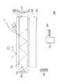
図1は、本発明の第一実施例によるタッチ投影システムを示す図である。図1を参照する。本実施例のタッチ投影システム1000は、投影ユニット100、スクリーン200、及びタッチ装置300を含む。投影ユニット100は、画像光束Lを提供するためのものである。画像光束Lとは、画像データを携帯する光束であって、且つ人の目により観察され得る光束を指す。スクリーン200は、画像光束Lの伝播経路に配置され、且つ画像光束Lを受けるためのものである。本実施例では、スクリーン200は、投影ユニット100とタッチ装置300の導光素子310との間に配置されてもよく、そのうち、導光素子310は、可透光性素子である。本実施例のスクリーン200は、相対する二つの表面210、220を有する。表面210は、表面220と導光素子310との間に位置する。表面210は、粗い(roughness)表面であり、スクリーン200に伝播(到着)した画像光束Lを乱反射(散乱)させることができ、これにより、各方向における使用者は、スクリーン200に表示されている画面を同時に鑑賞することができる。 FIG. 1 is a diagram illustrating a touch projection system according to a first embodiment of the present invention. Refer to FIG. The
本実施例におけるタッチ装置300は、画像光束Lの伝播経路に配置される。タッチ装置300は、導光素子310、発光素子320、不可視光フィルタリング層330、及び不可視光センサ340を含む。導光素子310は、少なくとも一つの入光面312、及び入光面312に接続される第一表面314を有する。発光素子320は、入光面312の近旁に配置され、且つ不可視光束Iを発するためのものであり、そのうち、不可視光束Iとは、人の目により観察することができない光束を指す。不可視光束Iは、入光面312から導光素子310に進入し、導光素子310の中に伝播する。更に言うと、本実施例の導光素子310の屈折率(例えば、1.52)は、空気の屈折率(例えば、1)より大きくなってもよく、これにより、不可視光束Iは、導光素子310と空気との界面において全反射され、導光素子310の中において全反射による伝播を行う。本実施例では、不可視光束Iは、例えば、赤外線光束である。上述の赤外線光束の波長範囲は、800nm〜1100nmである。しかし、本発明は、これに限定されない。 The
本実施例の不可視光フィルタリング層330は第一表面314と密に接触し、且つ不可視光フィルタリング層330は第一表面314のサイズに対応してもよい。導光素子310は、不可視光フィルタリング層330と不可視光センサ340との間に配置される。本実施例では、不可視光センサ340は、例えば、赤外線画像取得装置であり、そのうち、赤外線画像取得装置は、赤外線光束を電信号に変換するために用いられる。本実施例の不可視光フィルタリング層330は、複数の光学薄膜により積層されて形成されてもよく、且つ投影ユニット100がスクリーン200に投影した画像光束Lは、不可視光フィルタリング層330を通過することができ、これにより、使用者は、スクリーン200に表示されている画面を鑑賞することができる。図2は、図1における不可視光フィルタリング層の外部環境光に対する透過スペクトルを示す図である。図2から分かるように、波長が800nm〜1100nmにある外部環境光Sは、不可視光フィルタリング層330を通過することができない。換言すると、図1に示すように、波長が800nm〜1100nmにある外部環境光Sは、不可視光フィルタリング層330により反射され得るので、不可視光センサ340の中に進入しにくい。これにより、外部環境光Sがタッチ装置の信頼度及び感度に影響を与えやすいという従来技術の問題を解決することができる。 The invisible
図3は、図1における導光素子の第一表面と相対する側の表面において検出したスペクトル分布を示す図である。図1及び図3から分かるように、タッチ投影システム1000が外部環境光Sにより照射され且つ使用者がタッチ装置300をタッチしない時に、導光素子310の第一表面314が不可視光フィルタリング層330と密に接触する場合、導光素子310の第一表面314と相対する側の表面において、波長が400nm〜1000nmにある光束をほとんど検出していない。換言すると、不可視光フィルタリング層330の作用により、波長が800nm〜1100nmにある外部環境光Sは、不可視光センサ340の中にほとんど進入することができいので、タッチ投影システム1000のパフォーマンスにほとんど影響を与えず、且つ、波長範囲が400nm〜800nmである可視光は、不可視光センサ340中の可視光フィルタリング素子(図示せず)により遮られ、検出することができない。 FIG. 3 is a diagram showing a spectral distribution detected on the surface opposite to the first surface of the light guide element in FIG. As can be seen from FIGS. 1 and 3, when the
図4は、図1のタッチ投影システムを使用者がタッチした時の状態を示す図である。図4を参照する。使用者Pがタッチ装置300の不可視光フィルタリング層330をタッチした時に、導光素子310において、使用者Pが不可視光フィルタリング層330をタッチした位置に対応する不可視光束Iの全反射が破壊され得る。換言すると、導光素子310において、使用者Pが不可視光フィルタリング層330をタッチした位置に対応する不可視光束Iの全反射が破壊された後に、不可視光束Iは、使用者Pのタッチ位置に伝播(到着)し、且つ使用者Pにより散乱させられ得る。このようにして、不可視光センサ340は、使用者Pのタッチ位置の不可視光の強度が比較的に強いことを検出でき、これにより、使用者Pのタッチ位置を算出することができる。 FIG. 4 is a diagram illustrating a state when the user touches the touch projection system of FIG. Refer to FIG. When the user P touches the invisible
図5は、図4における導光素子の第一表面と相対する側の表面において検出したスペクトル分布を示す図である。図4及び図5を参照する。曲線S100は、使用者Pが不可視光フィルタリング層330をタッチした部分の屈折率が1.5である時に、上述の不可視光センサ340が検出したスペクトル分布を表し、曲線S200は、使用者Pが不可視光フィルタリング層330をタッチした部分の屈折率が2.5である時に、上述の不可視光センサ340が検出したスペクトル分布を表し、曲線S300は、使用者Pが不可視光フィルタリング層330をタッチした部分の屈折率が5である時に、上述の不可視光センサ340が検出したスペクトル分布を表し、曲線S400は、使用者Pが不可視光フィルタリング層330をタッチした部分の屈折率が10である時に、上述の不可視光センサ340が検出したスペクトル分布を表す。図3及び図5を比較すれば分かるように、使用者Pが不可視光フィルタリング層330をタッチした時に、本来導光素子310の中に伝播する不可視光は、使用者Pにより全反射が破壊された後に、不可視光センサ340が所在する一方側に伝播(到着)するので、不可視光センサ340によって検出され得る。不可視光センサ340が検出した不可視光の強度の変化を用いて、使用者Pがタッチした位置を算出することができる。 FIG. 5 is a diagram showing the spectral distribution detected on the surface of the light guide element in FIG. 4 opposite to the first surface. Please refer to FIG. 4 and FIG. Curve S100 represents the spectral distribution detected by the invisible
また、図1又は図4に示す導光素子310及び不可視光フィルタリング層330は、平板状である。しかし、本発明は、これに限定されず、他の実施例では、導光素子310及び不可視光フィルタリング層330は、弯曲状であってもよく、そのうち、不可視光フィルタリング層330は、導光素子310の第一表面314に沿って弯曲してもよい。この時に、不可視光フィルタリング層330は、波長範囲が赤外線である外部環境光Sの中の部分を遮蔽する機能を発揮することもでき、これにより、タッチ装置300のタッチ効果をより良くさせることができる。 Further, the
なお、本発明の実施例によるタッチ投影システムの表示装置では、スクリーンの位置は、図1又は図4に示す位置に限られない。他の実施例では、スクリーンは、他の位置に配置されてもよい。以下、図6を例として詳しく説明する。図6は、本発明のもう一つの実施例によるタッチ投影システムを示す図である。図6を参照する。この実施例によるタッチ投影システム1000Aは、図1又は図4に示すタッチ投影システム1000と類似するので、同じ素子は、同じ参照符号で示される。タッチ投影システム1000Aとタッチ投影システム1000との相違点は、スクリーン200Aの位置及構造がスクリーン200の位置及構造と異なることにある。詳しく言えば、タッチ投影システム1000Aでは、不可視光フィルタリング層330及び導光素子310は、投影ユニット100とスクリーン200Aと間に配置されてもよい。スクリーン200Aは、相対する二つの表面210A、220Aを有する。表面220Aは、表面210Aと不可視光フィルタリング層330との間に位置する。表面210Aは、粗い表面であってもよい。表面220Aは、不可視光フィルタリング層330に面して突起している複数の微細構造222を有し、これらの微細構造222は、互いの間に間隔が設置される。スクリーン200Aは、これらの突起している微細構造222により、不可視光フィルタリング層330に支えられ、且つ不可視光フィルタリング層330との間に隙間Tを形成することができる。 In the display device of the touch projection system according to the embodiment of the present invention, the position of the screen is not limited to the position shown in FIG. 1 or FIG. In other embodiments, the screen may be located at other locations. Hereinafter, FIG. 6 will be described in detail as an example. FIG. 6 is a diagram illustrating a touch projection system according to another embodiment of the present invention. Refer to FIG. Since the
なお、この実施例におけるスクリーン200Aは、可撓性(flexibility)を有する。使用者Pがタッチ投影システム1000Aをタッチしようとする時に、使用者Pは、スクリーン200Aを押圧することで、スクリーン200Aに変形を生じさせ、これにより、不可視光フィルタリング層330をタッチすることができる。スクリーン200Aは、良好な可撓性を有するので、使用者Pにより押圧されたスクリーン200Aの部分は、不可視光フィルタリング層330と密に接触することができ、これにより、タッチ投影システム1000Aのタッチ効果をより良くさせることができる。 Note that the
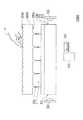
図7は、本発明の第二実施例によるタッチ投影システムを示す図である。図7を参照する。本実施例によるタッチ投影システム1000Bは、図1又は図4におけるタッチ投影システム1000と類似するので、同じ素子は、同じ参照符号で示される。タッチ投影システム1000Bとタッチ投影システム1000との相違点は、タッチ投影システム1000Bのタッチ装置300Bは遮光素子350を更に含むことにある。以下、この相違点について詳しく説明するが、両者の同じ部分について説明を省略する。 FIG. 7 is a diagram illustrating a touch projection system according to a second embodiment of the present invention. Refer to FIG. Since the
本実施例のタッチ投影システム1000Bでは、タッチ装置300Bは、少なくとも一つの遮光素子350を更に含んでもよい。遮光素子350は、導光素子310の第一表面314の辺縁に配置されてもよい。不可視光フィルタリング層330は、遮光素子350と第一表面314との間に配置されてもよい。コストのことを考慮すると、不可視光フィルタリング層330は、品質が普通である材料を採用してもよい。ところが、外部環境光Sが比較的大きい入射角(例えば、70度)で不可視光フィルタリング層330に入射する時に、一部の波長範囲の外部環境光Sは、不可視光フィルタリング層330を通過してタッチ投影システム1000Bのパフォーマンスに影響を与えることがある。しかし、遮光素子350の遮蔽作用により、入射角が比較的大きい外部環境光Sは、遮光素子350により、不可視光フィルタリング層330の外に遮蔽され得るので、本実施例によるタッチ投影システム1000Bは、低コスト及高パフォーマンスを兼備する。また、本実施例によるタッチ投影システム1000Bは、タッチ投影システム1000と類似する利点、機能及び効果を有するので、ここでは、その詳しい説明を省略する。 In the
図8は、本発明の第三実施例によるタッチ投影システムを示す図である。図8を参照する。本実施例によるタッチ投影システム1000Cは、第二実施例によるタッチ投影システム1000Bと類似するので、同じ素子は、同じ参照符号で示される。本実施例のタッチ投影システム1000Cと第二実施例のタッチ投影システム1000Bとの相違点は、タッチ投影システム1000Cのタッチ装置300Cは可撓性透光基板360を更に含むことにある。以下、この相違点について詳しく説明するが、両者の同じ部分について説明を省略する。 FIG. 8 is a diagram illustrating a touch projection system according to a third embodiment of the present invention. Refer to FIG. Since the
本実施例のタッチ投影システム1000Cでは、タッチ装置300Cは可撓性透光基板360を更に含む。不可視光フィルタリング層330は、可撓性透光基板360と導光素子310の第一表面314と間に配置されてもよい。更に言うと、可撓性透光基板360は、遮光素子350に固接されてもよく、また、可撓性透光基板360と不可視光フィルタリング層330との間は、隙間が存在してもよい。なお、可撓性透光基板360は、外部環境光Sを比較的小さい入射角で不可視光フィルタリング層330に伝播させ、不可視光フィルタリング層330に、外部環境光Sの中の不可視光成分を有効に阻止させ、これにより、タッチ投影システム1000Cのパフォーマンスを向上させることができる。また、画像光束Lは、可撓性透光基板360を通過した後に、比較的大きい出射角でタッチ投影システム1000Cから離れることができので、使用者は、広視野角の画面を鑑賞することができる。 In the
図9は、図8におけるタッチ投影システムを使用者がタッチした時の状態を示す図である。図9を参照する。使用者Pがタッチ投影システム1000Cをタッチしようとする時に、使用者Pは、可撓性透光基板360を押圧することで、それに変形を生じさせ、これにより、不可視光フィルタリング層330をタッチすることができる。可撓性透光基板360は、良好な可撓性を有するので、使用者Pにより押圧された可撓性透光基板360の部分は、不可視光フィルタリング層330と密に接触することができるので、タッチ投影システム1000Cのタッチ効果をより良くさせることができる。また、本実施例によるタッチ投影システム1000Cは、タッチ投影システム1000Bと類似する利点、機能、及び効果を有するので、ここでは、その詳しい説明を省略する。 FIG. 9 is a diagram illustrating a state when the user touches the touch projection system in FIG. Refer to FIG. When the user P tries to touch the
図10は、本発明の一実施例における不可視光フィルタリング層を示す図である。図10を参照する。この実施例における不可視光フィルタリング層330は、複数の光学薄膜により積層されて形成され、不可視光フィルタリング層330は、導光素子310と密に貼合される。そのうち、不可視光フィルタリング層330は、高屈折率光学薄膜332及び低屈折率光学薄膜334を含んで、両者を重複で積層することにより形成される。高屈折率光学薄膜332の屈折率はNhighであり、低屈折率光学薄膜334の屈折率はNlowであり、空気の屈折率はN0である。不可視光の波長範囲を有する外部環境光Sの中の光束Iは、空気から不可視光フィルタリング層330に入射し、各層の光学薄膜の界面において通過及び反射の行為を有するので、通過した不可視光の波長範囲の光束Iは、光の行程差により破壊的干渉が生じ、光強度が最低まで減少することができる。これにより、外部環境光Sは、可視光の波長範囲を有する光束(参照符号無し)のみが最後に導光素子310に伝播(到着)することができる。FIG. 10 is a diagram illustrating an invisible light filtering layer according to an embodiment of the present invention. Refer to FIG. The invisible
以上述べたところを総合すれば、本発明の一実施例によるタッチ装置及びタッチ投影システムは、不可視光フィルタリング層を利用して、外部環境光の中の不可視光成分が不可視光センサに進入するのを阻止することができる。これにより、本発明の実施例によるタッチ装置及びタッチ投影システムの信頼度及び感度を有効に向上させることができる。 In summary, the touch device and the touch projection system according to the embodiment of the present invention use the invisible light filtering layer to cause the invisible light component in the external environment light to enter the invisible light sensor. Can be prevented. Accordingly, the reliability and sensitivity of the touch device and the touch projection system according to the embodiment of the present invention can be effectively improved.
本発明のもう一つの実施例によるタッチ装置及びタッチ投影システムは、遮光素子により、入射角が比較的大きい外部環境光が不可視光フィルタリング層を通過するのを遮蔽することができる。これにより、外部環境光の中の不可視光成分が不可視光センサに伝播(到着)する確率を下げることで、本発明の他の実施例によるタッチ装置及びタッチ投影システムは、良好なパフォーマンスを有する。 The touch device and the touch projection system according to another embodiment of the present invention may shield external ambient light having a relatively large incident angle from passing through the invisible light filtering layer by the light shielding element. Accordingly, the touch device and the touch projection system according to another embodiment of the present invention have good performance by reducing the probability that the invisible light component in the external ambient light propagates (arrives) to the invisible light sensor.
また、本発明の他の実施例によるタッチ装置及びタッチ投影システムでは、使用者は、可撓性透光基板により、不可視光フィルタリング層を押圧することができる。可撓性透光基板は、良好な可撓性を有し、使用者により押圧された可撓性透光基板の部分は、不可視光フィルタリング層と密に接触することができるので、タッチ装置及びタッチ投影システムのタッチ効果をより良くさせることができる。 In addition, in the touch device and the touch projection system according to another embodiment of the present invention, the user can press the invisible light filtering layer with the flexible transparent substrate. The flexible translucent substrate has good flexibility, and the portion of the flexible translucent substrate pressed by the user can be in intimate contact with the invisible light filtering layer, so that the touch device and The touch effect of the touch projection system can be improved.
本発明は、前述した好適な実施例に基づいて以上のように開示されたが、前述した好適な実施例は、本発明を限定するためのものでなく、当業者は、本発明の精神と範囲を離脱しない限り、本発明に対して些細な変更と潤色を行うことができるので、本発明の保護範囲は、添付した特許請求の範囲に定まったものを基準とする。また、本発明の何れの実施例又は特許請求の範囲は、本発明に開示された全ての目の又は利点又は特徴を達成する必要がない。また、要約の部分と発明の名称は、文献の検索を助けるためのみのものであり、本発明の権利範囲を限定するものでない。また、本明細書又は特許請求の範囲に言及びしている「第一」、「第二」等の用語は、要素(element)に名前を付け、または、異なる実施例又は範囲を区別するためのもののみであり、要素の数量上の上限又は下限を限定するためのものでない。 Although the present invention has been disclosed above based on the preferred embodiments described above, the preferred embodiments described above are not intended to limit the present invention, and those skilled in the art will understand the spirit of the present invention. As long as the scope of the present invention is not deviated, minor modifications and color changes can be made to the present invention. Therefore, the protection scope of the present invention is based on what is defined in the appended claims. Moreover, any embodiment or claim of the invention need not achieve all eyes or advantages or features disclosed in the present invention. Further, the abstract part and the title of the invention are only for assisting the search of documents, and do not limit the scope of rights of the present invention. In addition, the terms “first”, “second”, etc. referred to in this specification or in the claims are used to name an element or to distinguish different embodiments or ranges. Are not intended to limit the upper or lower limit on the quantity of elements.
1000、1000A〜1000C:タッチ投影システム
100:投影ユニット
200、200A:スクリーン
210、220、210A、220A:表面
222:微細構造
300:タッチ装置
310:導光素子
312:入光面
314:第一表面
320:発光素子
330:不可視光フィルタリング層
332:高屈折率光学薄膜
334:低屈折率光学薄膜
340:不可視光センサ
350:遮光素子
360:可撓性透光基板
I:不可視光束
L:画像光束
Nlow:低屈折率光学薄膜の屈折率
Nhigh:高屈折率光学薄膜の屈折率
N0:空気の屈折率
P:使用者
S:外部環境光
T:隙間
S100〜S400:曲線1000, 1000A ~ 1000C: Touch projection system
100: Projection unit
200, 200A: Screen
210, 220, 210A, 220A: Surface
222: Microstructure
300: Touch device
310: Light guide element
312: Incident surface
314: First surface
320: Light emitting element
330: Invisible light filtering layer
332: High refractive index optical thin film
334: Low refractive index optical thin film
340: Invisible light sensor
350: Shading element
360: Flexible translucent substrate
I: Invisible luminous flux
L: Image luminous flux
Nlow : Refractive index of low refractive index optical thin film
Nhigh : Refractive index of high refractive index optical thin film
N0 : Refractive index of air
P: User
S: External ambient light
T: Clearance
S100 to S400: Curve
Claims (17)
Translated fromJapanese少なくとも一つの入光面及び前記入光面に接続される第一表面を有する導光素子と、
前記入光面の近旁に配置され且つ不可視光束を発する発光素子であって、前記不可視光束は前記入光面から前記導光素子に進入し前記導光素子の中に伝播する、発光素子と、
前記第一表面と密に接触し、前記第一表面のサイズに対応し、外部環境光が前記タッチ装置に進入することを阻止する不可視光フィルタリング層であって、前記外部環境光は波長範囲を有し、前記波長範囲は前記不可視光束の波長範囲に実質的に対応する、不可視光フィルタリング層と、
前記不可視光束を検出する不可視光センサと、を含み、
前記導光素子は、前記不可視光フィルタリング層と前記不可視光センサとの間に配置される、タッチ装置。A touch device,
A light guide element having at least one light incident surface and a first surface connected to the light incident surface;
A light emitting element disposed in the vicinity of the light incident surface and emitting an invisible light beam, wherein the invisible light beam enters the light guide element from the light incident surface and propagates into the light guide element; and
An invisible light filtering layer that is in intimate contact with the first surface, corresponds to a size of the first surface, and prevents external ambient light from entering the touch device, the external ambient light having a wavelength range; The wavelength range substantially corresponds to the wavelength range of the invisible light beam, and an invisible light filtering layer;
An invisible light sensor for detecting the invisible light flux,
The touch device, wherein the light guide element is disposed between the invisible light filtering layer and the invisible light sensor.
前記不可視光束は赤外線光束であり、前記不可視光センサは赤外線画像取得装置である、タッチ装置。The touch device according to claim 1, wherein
The touch device, wherein the invisible light beam is an infrared light beam, and the invisible light sensor is an infrared image acquisition device.
前記不可視光フィルタリング層は、複数の光学薄膜により積層されて形成される、タッチ装置。The touch device according to claim 1, wherein
The invisible light filtering layer is a touch device formed by laminating a plurality of optical thin films.
前記第一表面の辺縁に配置される少なくとも一つの遮光素子を更に含み、
前記不可視光フィルタリング層は、前記遮光素子と前記第一表面との間に配置される、タッチ装置。The touch device according to claim 1, wherein
And further comprising at least one light shielding element disposed on the edge of the first surface,
The touch device, wherein the invisible light filtering layer is disposed between the light shielding element and the first surface.
可撓性透光基板を更に含み、
前記不可視光フィルタリング層は、前記可撓性透光基板と前記第一表面との間に配置される、タッチ装置。The touch device according to claim 1, wherein
A flexible translucent substrate;
The touch device, wherein the invisible light filtering layer is disposed between the flexible translucent substrate and the first surface.
前記導光素子及び前記不可視光フィルタリング層は、弯曲状である、タッチ装置。The touch device according to claim 1, wherein
The touch device, wherein the light guide element and the invisible light filtering layer are curved.
画像光束を提供する投影ユニットと、
前記画像光束を受けるスクリーンと、
前記画像光束の伝播経路に配置されるタッチ装置と、を含み、
前記タッチ装置は、請求項1に記載のタッチ装置である、タッチ投影システム。A touch projection system,
A projection unit that provides image luminous flux;
A screen for receiving the image luminous flux;
A touch device disposed in the propagation path of the image light flux,
The touch projection system according to claim 1, wherein the touch device is a touch device according to claim 1.
前記スクリーンは、前記投影ユニットと前記導光素子との間に配置される、タッチ投影システム。The touch projection system according to claim 7, wherein
The touch projection system, wherein the screen is disposed between the projection unit and the light guide element.
前記不可視光フィルタリング層は、前記投影ユニットと前記スクリーンとの間に配置される、タッチ投影システム。The touch projection system according to claim 7, wherein
The touch projection system, wherein the invisible light filtering layer is disposed between the projection unit and the screen.
前記スクリーンは、可撓性を有する、タッチ投影システム。The touch projection system according to claim 9, wherein
The touch projection system, wherein the screen has flexibility.
前記スクリーンは、相対する第二表面及び第三表面を有し、前記第三表面は、前記導光素子と前記第二表面との間に位置し、前記第三表面は、粗い表面である、タッチ投影システム。The touch projection system according to claim 7, wherein
The screen has opposing second and third surfaces, the third surface is located between the light guide element and the second surface, and the third surface is a rough surface. Touch projection system.
前記スクリーンは、相対する第二表面及び第三表面を有し、前記第二表面は、前記不可視光フィルタリング層と前記第三表面との間に位置し、前記第三表面は、粗い表面であり、前記第二表面は、前記不可視光フィルタリング層に面して突起している複数の微細構造を有し、前記スクリーンは、前記複数の微細構造により、前記不可視光フィルタリング層に支えられる、タッチ投影システム。The touch projection system according to claim 9, wherein
The screen has opposite second and third surfaces, the second surface is located between the invisible light filtering layer and the third surface, and the third surface is a rough surface. Wherein the second surface has a plurality of microstructures projecting toward the invisible light filtering layer, and the screen is supported by the invisible light filtering layer by the plurality of microstructures. system.
前記不可視光束は赤外線光束であり、前記不可視光センサは赤外線画像取得装置である、タッチ投影システム。The touch projection system according to claim 7, wherein
The touch projection system, wherein the invisible light beam is an infrared light beam, and the invisible light sensor is an infrared image acquisition device.
前記不可視光フィルタリング層は、複数の光学薄膜により積層されて形成される、タッチ投影システム。The touch projection system according to claim 7, wherein
The invisible light filtering layer is a touch projection system formed by laminating a plurality of optical thin films.
前記タッチ装置は、前記第一表面の辺縁に配置される少なくとも一つの遮光素子を更に含み、
前記不可視光フィルタリング層は、前記遮光素子と前記第一表面との間に配置される、タッチ投影システム。The touch projection system according to claim 7, wherein
The touch device further includes at least one light shielding element disposed on an edge of the first surface,
The touch projection system, wherein the invisible light filtering layer is disposed between the light shielding element and the first surface.
前記タッチ装置は、可撓性透光基板を更に含み、
前記不可視光フィルタリング層は、前記可撓性透光基板と前記第一表面との間に配置される、タッチ投影システム。The touch projection system according to claim 7, wherein
The touch device further includes a flexible translucent substrate,
The touch projection system, wherein the invisible light filtering layer is disposed between the flexible translucent substrate and the first surface.
前記導光素子及び前記不可視光フィルタリング層は、弯曲状である、タッチ投影システム。The touch projection system according to claim 7, wherein
The touch projection system, wherein the light guide element and the invisible light filtering layer are curved.
Applications Claiming Priority (2)
| Application Number | Priority Date | Filing Date | Title |
|---|---|---|---|
| TW101112644ATWI543045B (en) | 2012-04-10 | 2012-04-10 | Touch device and touch projection system using the same |
| TW101112644 | 2012-04-10 |
Publications (1)
| Publication Number | Publication Date |
|---|---|
| JP2013218677Atrue JP2013218677A (en) | 2013-10-24 |
Family
ID=49210047
Family Applications (1)
| Application Number | Title | Priority Date | Filing Date |
|---|---|---|---|
| JP2013059200APendingJP2013218677A (en) | 2012-04-10 | 2013-03-22 | Touch device and touch projection system |
Country Status (5)
| Country | Link |
|---|---|
| US (1) | US9213444B2 (en) |
| JP (1) | JP2013218677A (en) |
| CN (1) | CN103365487B (en) |
| DE (1) | DE102013103383B4 (en) |
| TW (1) | TWI543045B (en) |
Families Citing this family (3)
| Publication number | Priority date | Publication date | Assignee | Title |
|---|---|---|---|---|
| US10901548B2 (en)* | 2015-04-07 | 2021-01-26 | Omnivision Technologies, Inc. | Touch screen rear projection display |
| CN106406639B (en)* | 2016-09-12 | 2024-04-09 | 合肥京东方光电科技有限公司 | Touch screen, touch display device and touch detection method |
| CN109753190B (en)* | 2018-12-28 | 2022-01-07 | 惠科股份有限公司 | Touch device, display device and touch detection method |
Citations (3)
| Publication number | Priority date | Publication date | Assignee | Title |
|---|---|---|---|---|
| JP2009545828A (en)* | 2006-08-03 | 2009-12-24 | パーセプティブ ピクセル,インク. | Multi-contact detection display device with total reflection interference |
| US20100302185A1 (en)* | 2009-06-01 | 2010-12-02 | Perceptive Pixel Inc. | Touch Sensing |
| JP2011527478A (en)* | 2008-07-07 | 2011-10-27 | ノーテル ネットワークス リミテッド | Multi-touch touch screen with pen tracking |
Family Cites Families (18)
| Publication number | Priority date | Publication date | Assignee | Title |
|---|---|---|---|---|
| US5360659A (en)* | 1993-05-24 | 1994-11-01 | The Dow Chemical Company | Two component infrared reflecting film |
| KR20040010328A (en) | 2002-07-24 | 2004-01-31 | 소니 가부시끼 가이샤 | Projection screen and its manufacturing method |
| US7521666B2 (en)* | 2005-02-17 | 2009-04-21 | Capella Microsystems Inc. | Multi-cavity Fabry-Perot ambient light filter apparatus |
| US7705835B2 (en)* | 2005-03-28 | 2010-04-27 | Adam Eikman | Photonic touch screen apparatus and method of use |
| TWI334958B (en)* | 2006-06-08 | 2010-12-21 | Delta Electronics Inc | Projection screen |
| US8441467B2 (en)* | 2006-08-03 | 2013-05-14 | Perceptive Pixel Inc. | Multi-touch sensing display through frustrated total internal reflection |
| US8144271B2 (en)* | 2006-08-03 | 2012-03-27 | Perceptive Pixel Inc. | Multi-touch sensing through frustrated total internal reflection |
| CN101821703A (en) | 2007-08-03 | 2010-09-01 | 感知像素股份有限公司 | Multi-touch sensing through frustrated total internal reflection |
| WO2009110284A1 (en) | 2008-03-03 | 2009-09-11 | 日本電気株式会社 | Channel switching device, method threrfor and program therefor |
| TW200945123A (en)* | 2008-04-25 | 2009-11-01 | Ind Tech Res Inst | A multi-touch position tracking apparatus and interactive system and image processing method there of |
| CN102308267A (en) | 2009-05-28 | 2012-01-04 | 夏普株式会社 | Touch panel, liquid crystal panel, liquid crystal display device, and liquid crystal display device incorporating touch panel |
| US8736581B2 (en) | 2009-06-01 | 2014-05-27 | Perceptive Pixel Inc. | Touch sensing with frustrated total internal reflection |
| JP2011175618A (en)* | 2010-01-29 | 2011-09-08 | Japan Aviation Electronics Industry Ltd | Optical touch panel |
| TW201202770A (en) | 2010-07-09 | 2012-01-16 | Global Lighting Technology Inc | Light guide device and back light module having the same |
| US8816963B2 (en)* | 2010-12-13 | 2014-08-26 | Sae Magnetics (H.K.) Ltd. | Optical navigation module and mobile electronic appliance using optical navigation module |
| US8619062B2 (en)* | 2011-02-03 | 2013-12-31 | Microsoft Corporation | Touch-pressure sensing in a display panel |
| TW201307916A (en)* | 2011-08-08 | 2013-02-16 | Primax Electronics Ltd | Input device with multi layers luminous patterns |
| US20130234990A1 (en)* | 2012-03-06 | 2013-09-12 | Smart Technologies Ulc | Interactive input system and method |
- 2012
- 2012-04-10TWTW101112644Apatent/TWI543045B/enactive
- 2012-08-16USUS13/587,894patent/US9213444B2/enactiveActive
- 2013
- 2013-03-21CNCN201310091041.1Apatent/CN103365487B/enactiveActive
- 2013-03-22JPJP2013059200Apatent/JP2013218677A/enactivePending
- 2013-04-04DEDE102013103383.0Apatent/DE102013103383B4/enactiveActive
Patent Citations (3)
| Publication number | Priority date | Publication date | Assignee | Title |
|---|---|---|---|---|
| JP2009545828A (en)* | 2006-08-03 | 2009-12-24 | パーセプティブ ピクセル,インク. | Multi-contact detection display device with total reflection interference |
| JP2011527478A (en)* | 2008-07-07 | 2011-10-27 | ノーテル ネットワークス リミテッド | Multi-touch touch screen with pen tracking |
| US20100302185A1 (en)* | 2009-06-01 | 2010-12-02 | Perceptive Pixel Inc. | Touch Sensing |
Also Published As
| Publication number | Publication date |
|---|---|
| US20130265245A1 (en) | 2013-10-10 |
| CN103365487B (en) | 2017-03-01 |
| TWI543045B (en) | 2016-07-21 |
| US9213444B2 (en) | 2015-12-15 |
| DE102013103383A1 (en) | 2013-10-10 |
| DE102013103383B4 (en) | 2024-07-18 |
| CN103365487A (en) | 2013-10-23 |
| TW201342159A (en) | 2013-10-16 |
Similar Documents
| Publication | Publication Date | Title |
|---|---|---|
| TWI451311B (en) | Touch-sensing display device | |
| JP5174962B2 (en) | Touch panel, liquid crystal panel, liquid crystal display device, and touch panel integrated liquid crystal display device | |
| TWI522869B (en) | Optical touch display apparatus | |
| CN101582001A (en) | Touch screen, touch module and control method | |
| TWI571769B (en) | Contactless input device and method | |
| US8493365B2 (en) | Optical touch display apparatus | |
| US20140055418A1 (en) | Touch display panel and optical touch panel thereof | |
| TWI472962B (en) | Input device | |
| US20150035799A1 (en) | Optical touchscreen | |
| CN102662527B (en) | Touch Sensing Display Device | |
| US20150205442A1 (en) | Optical touch screen | |
| US20150317034A1 (en) | Water-immune ftir touch screen | |
| TWM517370U (en) | Optical touch control apparatus | |
| TWI438669B (en) | Optical touch module and method thereof | |
| CN102117151B (en) | Optical touch display device | |
| JP2013218677A (en) | Touch device and touch projection system | |
| TWI433012B (en) | Optical touch display and optical operation apparatus | |
| JP5368731B2 (en) | Touch panel | |
| JP2011122870A (en) | Optical position detection device and projection display device | |
| TWI502417B (en) | Touch display apparatus and operation method thereof | |
| TWI559193B (en) | Optical touch screens | |
| CN102122217B (en) | Optical touch display device | |
| TWI471785B (en) | Optical touch module | |
| CN102129330A (en) | Touch screen, touch module and control method | |
| CN103309519B (en) | Touch position detection method and optical touch device using same |
Legal Events
| Date | Code | Title | Description |
|---|---|---|---|
| A131 | Notification of reasons for refusal | Free format text:JAPANESE INTERMEDIATE CODE: A131 Effective date:20140401 | |
| A521 | Request for written amendment filed | Free format text:JAPANESE INTERMEDIATE CODE: A523 Effective date:20140630 | |
| A02 | Decision of refusal | Free format text:JAPANESE INTERMEDIATE CODE: A02 Effective date:20150106 | |
| A521 | Request for written amendment filed | Free format text:JAPANESE INTERMEDIATE CODE: A523 Effective date:20150422 | |
| A911 | Transfer to examiner for re-examination before appeal (zenchi) | Free format text:JAPANESE INTERMEDIATE CODE: A911 Effective date:20150430 | |
| A912 | Re-examination (zenchi) completed and case transferred to appeal board | Free format text:JAPANESE INTERMEDIATE CODE: A912 Effective date:20150717 |