JP2013214909A - Vehicle mobile equipment - Google Patents
Vehicle mobile equipmentDownload PDFInfo
- Publication number
- JP2013214909A JP2013214909AJP2012085000AJP2012085000AJP2013214909AJP 2013214909 AJP2013214909 AJP 2013214909AJP 2012085000 AJP2012085000 AJP 2012085000AJP 2012085000 AJP2012085000 AJP 2012085000AJP 2013214909 AJP2013214909 AJP 2013214909A
- Authority
- JP
- Japan
- Prior art keywords
- antenna
- film layer
- portable device
- vehicle
- field communication
- Prior art date
- Legal status (The legal status is an assumption and is not a legal conclusion. Google has not performed a legal analysis and makes no representation as to the accuracy of the status listed.)
- Pending
Links
- 238000004891communicationMethods0.000claimsabstractdescription46
- 238000007639printingMethods0.000claimsabstractdescription11
- 239000011347resinSubstances0.000claimsdescription16
- 229920005989resinPolymers0.000claimsdescription16
- 230000000149penetrating effectEffects0.000claimsdescription2
- 238000005034decorationMethods0.000abstract1
- 239000000758substrateSubstances0.000description18
- 238000000465mouldingMethods0.000description6
- 238000000034methodMethods0.000description5
- 238000010586diagramMethods0.000description2
- 230000002093peripheral effectEffects0.000description2
- 238000007650screen-printingMethods0.000description2
- 230000004308accommodationEffects0.000description1
- 239000000463materialSubstances0.000description1
- 229920000515polycarbonatePolymers0.000description1
- 239000004417polycarbonateSubstances0.000description1
- 238000005476solderingMethods0.000description1
Images


Classifications
- G—PHYSICS
- G07—CHECKING-DEVICES
- G07C—TIME OR ATTENDANCE REGISTERS; REGISTERING OR INDICATING THE WORKING OF MACHINES; GENERATING RANDOM NUMBERS; VOTING OR LOTTERY APPARATUS; ARRANGEMENTS, SYSTEMS OR APPARATUS FOR CHECKING NOT PROVIDED FOR ELSEWHERE
- G07C9/00—Individual registration on entry or exit
- G07C9/00174—Electronically operated locks; Circuits therefor; Nonmechanical keys therefor, e.g. passive or active electrical keys or other data carriers without mechanical keys
- G07C9/00309—Electronically operated locks; Circuits therefor; Nonmechanical keys therefor, e.g. passive or active electrical keys or other data carriers without mechanical keys operated with bidirectional data transmission between data carrier and locks
- G—PHYSICS
- G07—CHECKING-DEVICES
- G07C—TIME OR ATTENDANCE REGISTERS; REGISTERING OR INDICATING THE WORKING OF MACHINES; GENERATING RANDOM NUMBERS; VOTING OR LOTTERY APPARATUS; ARRANGEMENTS, SYSTEMS OR APPARATUS FOR CHECKING NOT PROVIDED FOR ELSEWHERE
- G07C9/00—Individual registration on entry or exit
- G07C9/00174—Electronically operated locks; Circuits therefor; Nonmechanical keys therefor, e.g. passive or active electrical keys or other data carriers without mechanical keys
- G07C9/00944—Details of construction or manufacture
- H—ELECTRICITY
- H01—ELECTRIC ELEMENTS
- H01Q—ANTENNAS, i.e. RADIO AERIALS
- H01Q1/00—Details of, or arrangements associated with, antennas
- H01Q1/27—Adaptation for use in or on movable bodies
- H01Q1/32—Adaptation for use in or on road or rail vehicles
- H01Q1/3208—Adaptation for use in or on road or rail vehicles characterised by the application wherein the antenna is used
- H01Q1/3233—Adaptation for use in or on road or rail vehicles characterised by the application wherein the antenna is used particular used as part of a sensor or in a security system, e.g. for automotive radar, navigation systems
- H01Q1/3241—Adaptation for use in or on road or rail vehicles characterised by the application wherein the antenna is used particular used as part of a sensor or in a security system, e.g. for automotive radar, navigation systems particular used in keyless entry systems
- H—ELECTRICITY
- H01—ELECTRIC ELEMENTS
- H01Q—ANTENNAS, i.e. RADIO AERIALS
- H01Q1/00—Details of, or arrangements associated with, antennas
- H01Q1/40—Radiating elements coated with or embedded in protective material
- G—PHYSICS
- G07—CHECKING-DEVICES
- G07C—TIME OR ATTENDANCE REGISTERS; REGISTERING OR INDICATING THE WORKING OF MACHINES; GENERATING RANDOM NUMBERS; VOTING OR LOTTERY APPARATUS; ARRANGEMENTS, SYSTEMS OR APPARATUS FOR CHECKING NOT PROVIDED FOR ELSEWHERE
- G07C9/00—Individual registration on entry or exit
- G07C9/00174—Electronically operated locks; Circuits therefor; Nonmechanical keys therefor, e.g. passive or active electrical keys or other data carriers without mechanical keys
- G07C9/00309—Electronically operated locks; Circuits therefor; Nonmechanical keys therefor, e.g. passive or active electrical keys or other data carriers without mechanical keys operated with bidirectional data transmission between data carrier and locks
- G07C2009/00341—Electronically operated locks; Circuits therefor; Nonmechanical keys therefor, e.g. passive or active electrical keys or other data carriers without mechanical keys operated with bidirectional data transmission between data carrier and locks keyless data carrier having more than one limited data transmission ranges
- G07C2009/00357—Electronically operated locks; Circuits therefor; Nonmechanical keys therefor, e.g. passive or active electrical keys or other data carriers without mechanical keys operated with bidirectional data transmission between data carrier and locks keyless data carrier having more than one limited data transmission ranges and the lock having more than one limited data transmission ranges
- G—PHYSICS
- G07—CHECKING-DEVICES
- G07C—TIME OR ATTENDANCE REGISTERS; REGISTERING OR INDICATING THE WORKING OF MACHINES; GENERATING RANDOM NUMBERS; VOTING OR LOTTERY APPARATUS; ARRANGEMENTS, SYSTEMS OR APPARATUS FOR CHECKING NOT PROVIDED FOR ELSEWHERE
- G07C9/00—Individual registration on entry or exit
- G07C9/00174—Electronically operated locks; Circuits therefor; Nonmechanical keys therefor, e.g. passive or active electrical keys or other data carriers without mechanical keys
- G07C2009/00753—Electronically operated locks; Circuits therefor; Nonmechanical keys therefor, e.g. passive or active electrical keys or other data carriers without mechanical keys operated by active electrical keys
- G07C2009/00769—Electronically operated locks; Circuits therefor; Nonmechanical keys therefor, e.g. passive or active electrical keys or other data carriers without mechanical keys operated by active electrical keys with data transmission performed by wireless means
- H—ELECTRICITY
- H01—ELECTRIC ELEMENTS
- H01Q—ANTENNAS, i.e. RADIO AERIALS
- H01Q7/00—Loop antennas with a substantially uniform current distribution around the loop and having a directional radiation pattern in a plane perpendicular to the plane of the loop
Landscapes
- Engineering & Computer Science (AREA)
- Physics & Mathematics (AREA)
- General Physics & Mathematics (AREA)
- Computer Security & Cryptography (AREA)
- Radar, Positioning & Navigation (AREA)
- Remote Sensing (AREA)
- Manufacturing & Machinery (AREA)
- Computer Networks & Wireless Communication (AREA)
- Lock And Its Accessories (AREA)
- Support Of Aerials (AREA)
- Telephone Set Structure (AREA)
Abstract
Description
Translated fromJapanese本発明は、車両用携帯機に関し、特に、近接場通信も可能な車両用携帯機に関する。 The present invention relates to a vehicular portable device, and more particularly to a vehicular portable device capable of near-field communication.
車両に搭載されている無線機との間で近距離無線通信を行なって、車両ドアの施錠、解錠等、車載機器を遠隔制御する車両用携帯機が知られている。 2. Description of the Related Art There is known a vehicular portable device that performs short-range wireless communication with a wireless device mounted on a vehicle to remotely control an in-vehicle device such as locking and unlocking a vehicle door.
また、近距離無線通信に加えて、近接場通信(Near Field Communication:NFC)も可能な車両用携帯機も知られている。なお、「近距離無線通信」は、「近接場通信」の意味で用いられることもあるが、本明細書では、「近距離無線通信」を「近接場通信」よりは通信距離が長い近距離の無線通信の意味で用いる。 In addition to the short-range wireless communication, a vehicular portable device capable of near field communication (NFC) is also known. Note that “near field communication” is sometimes used in the meaning of “near field communication”, but in this specification, “near field communication” is a near field having a longer communication distance than “near field communication”. It is used to mean wireless communication.
通信距離の異なる2種類の無線通信のうちの一方としてNFCが可能な通信機としては、携帯電話機が広く知られている。たとえば、特許文献1に開示の携帯電話機では、NFC用のアンテナに相当するRFID用アンテナを、電池蓋8の内面に貼り付けている。 A mobile phone is widely known as a communication device capable of NFC as one of two types of wireless communication having different communication distances. For example, in the mobile phone disclosed in
近距離無線通信と近接場通信の2つの通信を可能にするためには、それぞれの通信用に2つのアンテナが必要となる。しかし、車両用携帯機は小さいことから、2つのアンテナをどこに配置するかが問題となる。 In order to enable two types of communication, near field communication and near field communication, two antennas are required for each communication. However, since the vehicular portable device is small, the problem is where to place the two antennas.
たとえば、2つのアンテナをともに基板上に配置することが考えられる。しかし、基板には、種々の電子部品や電池等も配置されることから、アンテナを配置する場所はかなり制限される。また、前述の特許文献1には、電池蓋8の内面にアンテナを貼り付ける技術が開示されている。蓋の内面にアンテナを貼り付ければ、基板にアンテナを設けるよりは、大きいアンテナを配置することができる。しかし、蓋は、その蓋が組み合わせられるケースと接合する枠を備えるのが通常であり、特許文献1に開示の電池蓋8もこの枠を備えている。蓋の内面にアンテナを貼り付けるとしても、この枠内にしか貼り付けることができないので、枠の内周サイズよりも小さいアンテナしか貼り付けることができない。しかも、特許文献1の電池蓋8には、強度確保のための複数の梁も蓋内面に形成されている。特許文献1の例に限らず、一般的に、蓋の内面には梁等の種々の突起が形成されている。蓋の内面にアンテナを貼り付ける場合、蓋に形成されている枠の内側に貼り付け場所が限られることに加え、さらに、これらの突起が形成されていない部分に貼り付け場所が限られる。よって、蓋の内面にアンテナを貼り付けるとしても、蓋よりもかなり小さいアンテナとなってしまう。 For example, it is conceivable to arrange two antennas on the substrate. However, since various electronic components, batteries, and the like are also arranged on the substrate, the place where the antenna is arranged is considerably limited. Further,
本発明は、この事情に基づいて成されたものであり、その目的とするところは、より大きい近接場通信用アンテナを備えることができる車両用携帯機を提供することにある。 The present invention has been made based on this situation, and an object thereof is to provide a portable device for a vehicle that can be provided with a larger near-field communication antenna.
その目的を達成するための本発明は、車両に搭載されている通信機との間での近距離無線通信に用いられる近距離用アンテナ(11)と、この近距離通信アンテナを収容する収容ケース(5、6、7)とを備えた車両用携帯機(1)であって、
前記収容ケースに、近接場通信用アンテナ(40)が加飾印刷されていることを特徴とする。In order to achieve the object, the present invention provides a short-range antenna (11) used for short-range wireless communication with a communication device mounted on a vehicle, and a storage case for storing the short-range communication antenna. (5, 6, 7), a portable device for a vehicle (1),
A near-field communication antenna (40) is decorated and printed on the housing case.
このように、本発明では、近接場通信用アンテナは収容ケースに加飾印刷されていることから、収容ケースの枠等、収容ケースの内側形状の影響を受けずに近接場通信用アンテナを配置することができる。よって、より大きい近接場通信用アンテナを車両用携帯機に設けることができる。 As described above, in the present invention, since the near-field communication antenna is decorated and printed on the housing case, the near-field communication antenna is arranged without being affected by the inner shape of the housing case, such as the frame of the housing case. can do. Therefore, a larger near-field communication antenna can be provided in the vehicle portable device.
(第1実施形態)
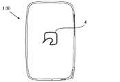
以下、本発明の実施形態を図面に基づいて説明する。図1、2に示す車両用携帯機(以下、単に携帯機)1は、平面視において略矩形の形状であり、スイッチ面(図1)には、車両ドアの施錠を指示する際にユーザが操作する施錠スイッチ2と、解錠を指示する際にユーザが操作する解錠スイッチ3が設けられている。一方、裏面(図2)には、加飾印刷されたマーク4が外観可能となっている。なお、図2に示すマーク4は、フェリカネットワークス株式会社の登録商標である。(First embodiment)
Hereinafter, embodiments of the present invention will be described with reference to the drawings. 1 and 2 has a substantially rectangular shape in plan view, and the switch surface (FIG. 1) has a user's instruction when locking the vehicle door. An
図1は携帯機1のスイッチ側ケース5の平面図でもあり、また、図2は携帯機1の裏面側ケース6の平面図でもある。これらスイッチ側ケース5と裏面側ケース6とにより、略直方体形状の収容ケース7が構成される。 FIG. 1 is a plan view of the switch-
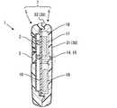
この収容ケース7の内部には、図3、4に示す基板10などが収容される。この基板10の一方の面(裏面側ケース対向面)には、図4に示すように、3軸アンテナ11が配置される。3軸アンテナ11は、近距離無線通信に用いられる近距離用アンテナであり、施錠スイッチ2、解錠スイッチ3が押圧操作された場合には、この3軸アンテナ11から電波が送信される。 The
また、基板10の裏面側ケース対向面には電池配置部50も形成されている。この電池配置部50には電池19(図5参照)が配置される。さらに、この面には、後述するNFCアンテナ40と接続する一対の基板側端子12、13も形成されている。また、この基板側端子12、13に一体化されて、板ばね状の接点ばね14、15が形成されている。なお、接点ばね14、15としてコイルばねを用いることも、もちろん可能である。 In addition, a
基板10の他方の面(スイッチ側ケース対向面)には、図3に示すように、スイッチ接点16、17が形成されている。このスイッチ接点16、17は、それぞれ、施錠スイッチ2、解錠スイッチ3に対応しており、一方のスイッチ接点16は施錠スイッチ2の押圧操作により導通し、他方のスイッチ接点17は解錠スイッチ3の押圧操作により導通する。また、図示していなが、基板10のスイッチ側ケース対向面には、近距離無線通信用回路、NFC通信用回路などの種々の電子部品が配置される。 As shown in FIG. 3,
図5の断面図に示すように、スイッチ側ケース5および裏面側ケース6は、いずれも、一方向に開口する浅型箱体であり、これらが、互いの開口が対向する向きで組み合わせられることにより携帯機1の内部に収容室18が形成される。この収容室18に、基板10、3軸アンテナ11、電池19などが収容される。 As shown in the cross-sectional view of FIG. 5, both the
また、スイッチ側ケース5および裏面側ケース6は、いずれも、ベース樹脂部の表面にフィルム層を有し、且つ、フィルム層とベース樹脂部との間に印刷層を有する構造である。この構造のスイッチ側ケース5、裏面側ケース6は、フィルムインサート成形法により成形される。 Each of the
このフィルムインサート成形法は、フィルム層および加飾層をベース樹脂部とともに一体成形する成形方法である。なお、フィルムインサート成形法は周知であるので、詳細説明は省略する。フィルム層には、たとえば、ポリカーボネートなどの透明樹脂が用いられる。 This film insert molding method is a molding method in which a film layer and a decorative layer are integrally molded together with a base resin portion. Since the film insert molding method is well known, detailed description is omitted. For the film layer, for example, a transparent resin such as polycarbonate is used.
さらに、裏面側ケース6は、アンテナ印刷層24等も備えている。詳しくは、図6に示すように、裏面側ケース6は、外側から順に、外側フィルム層21、加飾印刷層22、内側ルム層23、アンテナ印刷層24が積層されており、アンテナ印刷層24の下(ケース内側)にベース樹脂部30が存在する。 Further, the
図5に示すように、ベース樹脂部30の形状は、裏面側ケース6の形状とほぼ同じであり、浅型箱体であって、上述の外側フィルム層21等が設けられる底部31と、底部31の外周縁に形成された枠部32を備える。 As shown in FIG. 5, the shape of the
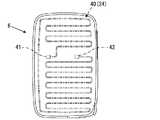
アンテナ印刷層24にはNFCアンテナ40が形成されている。このNFCアンテナ40は、たとえばスクリーン印刷により形成される。また、加飾印刷層22も、同様に、スクリーン印刷により意匠が印刷される。 An
そして、フィルム層、印刷層が各1層である通常の場合と同様に、全部が積層された状態でフィルムインサート成形により一体成形される。また、外側フィルム層21、内側フィルム層23には、通常のフィルム層と同じ材料を用いる。なお、フィルム層は、透明樹脂が一般的であるが、有色樹脂を用いることとしてもよい。これらフィルム層21、23の厚さは、たとえば、0.2〜0.3mm程度である。一方、印刷層22、24の厚さは、たとえば、10μm程度である。 And like the normal case where a film layer and a printing layer are one each, it is integrally formed by film insert molding in the state where all were laminated. Moreover, the same material as a normal film layer is used for the
外側フィルム層21、加飾印刷層22、内側フィルム層23、アンテナ印刷層24はベース樹脂部30の外面のほぼ全面に形成される。つまり、アンテナ印刷層24も、ベース樹脂部30の外面のほぼ全面に形成される。 The
図7にはアンテナ印刷層24を示しており、この図7に示すように、NFCアンテナ40の配置範囲を裏面側ケース6のほぼ全面とすることができる。このNFCアンテナ40において、2つのアンテナ端41、42は、基板10に設けられた基板側端子12、13にそれぞれ対向する位置に設けられている。また、ベース樹脂部30のアンテナ端41、42が設けられている部分は、図5、6に示すように、厚さ方向に貫通する貫通穴33が形成されており、アンテナ端41、42は、収容室18に露出している。また、貫通穴33が設けられているものの、この貫通穴33は、外側フィルム層21、加飾印刷層22、内側フィルム層23、アンテナ印刷層24には形成されていないので、収容室18の防水性は保持される。 FIG. 7 shows the
基板側端子12、13と一体化している接点ばね14、15は、この貫通穴33を貫通してアンテナ端41、42に接触する(図5参照)。これにより、NFCアンテナ40のアンテナ端41、42と基板側端子12、13とは導通している。 The contact springs 14 and 15 integrated with the board-
以上、説明した本実施形態によれば、NFCアンテナ40は裏面側ケース6に加飾印刷されていることから、裏面側ケース6のベース樹脂部30の枠部32等、裏面側ケース6の内側形状の影響を受けずにNFCアンテナ40を配置することができる。よって、図7に示したように、NFCアンテナ40の配置範囲を裏面側ケース6のほぼ全面とすることができる。つまり、基板10のサイズや、ベース樹脂部30の枠部32の内周サイズよりも大きいNFCアンテナ40を携帯機1に設けることができる。 As described above, according to the embodiment described above, the
しかも、アンテナ印刷層24は、基板10に比べて収容ケース7の表面に近い位置に存在することから、基板10にアンテナを設ける場合よりも、NFC通信を行なう通信相手装置に備えられているアンテナとの距離を近くすることができる。よって、携帯機1それ自体は、基板10にアンテナを設ける場合よりも離した状態でNFC通信が可能となる。 Moreover, since the
また、本実施形態では、裏面側ケース6は、外側フィルム層21、内側フィルム層23の2つのフィルム層を備えており、内側フィルム層23の内側に、NFCアンテナ40が形成されているアンテナ印刷層24を備えている。そのため、裏面側ケース6の成形時に圧力が加わる際に、表面にNFCアンテナ40のパターン形状の凹凸が出てしまうことが抑制される。 In the present embodiment, the
また、本実施形態では、接点ばね14、15により、NFCアンテナ40のアンテナ端41、42と基板10に形成された基板側端子12、13とが導通している。よって、導線をはんだ付けすることで両者を導通させる場合と異なり、電池交換の際に、スイッチ側ケース5と裏面側ケース6とを距離の制約なく離隔させることができる。そのため、電池交換作業が容易になる。 In the present embodiment, the antenna springs 41 and 42 of the
(第2実施形態)
たとえば、前述の実施形態では、2つのフィルム層21、23を備えていたが、内側フィルム層をなくし、フィルム層を外側フィルム層のみとしてもよい。フィルム層を1層のみとすれば、コストを低減することができる。なお、フィルム層を外側フィルム層のみとする場合、外側フィルム層の厚さは、第1実施形態の同様としてもよいし、また、第1実施形態よりも厚くしてもよい。たとえば、第1実施形態の2つのフィルム層分の厚さとしてもよい。(Second Embodiment)
For example, in the above-described embodiment, the two film layers 21 and 23 are provided, but the inner film layer may be eliminated and the film layer may be only the outer film layer. If only one film layer is used, the cost can be reduced. When only the outer film layer is used as the film layer, the thickness of the outer film layer may be the same as that of the first embodiment or may be thicker than that of the first embodiment. For example, it may be the thickness of the two film layers of the first embodiment.
以上、本発明の実施形態を説明したが、本発明は上述の実施形態に限定されるものではなく、要旨を逸脱しない範囲内で種々変更して実施することができる。 As mentioned above, although embodiment of this invention was described, this invention is not limited to the above-mentioned embodiment, It can implement in various changes within the range which does not deviate from a summary.
1:車両用携帯機、 2:施錠スイッチ、 3:解錠スイッチ、 4:マーク、 5:スイッチ側ケース、 6:裏面側ケース、 7:収容ケース、 10:基板、 11:3軸アンテナ(近距離用アンテナ)、 12:基板側端子、 13:基板側端子、 14:接点ばね、 15:接点ばね、 16:スイッチ接点、 17:スイッチ接点、 18:収容室、 19:電池、 21:外側フィルム層、 22:加飾印刷層、 23:内側フィルム層、 24:アンテナ印刷層、 30:ベース樹脂部、 31:底部、 32:枠部、 33:貫通穴、 40:NFCアンテナ(近接場通信用アンテナ)、 41:アンテナ端、 42:アンテナ端、 50:電池配置部1: vehicle portable device, 2: lock switch, 3: unlock switch, 4: mark, 5: switch side case, 6: back side case, 7: housing case, 10: substrate, 11: 3-axis antenna (near Antenna for distance), 12: substrate side terminal, 13: substrate side terminal, 14: contact spring, 15: contact spring, 16: switch contact, 17: switch contact, 18: storage chamber, 19: battery, 21: outer film Layer: 22: decorative printing layer, 23: inner film layer, 24: antenna printing layer, 30: base resin part, 31: bottom part, 32: frame part, 33: through hole, 40: NFC antenna (for near field communication) Antenna), 41: antenna end, 42: antenna end, 50: battery placement part
Claims (3)
Translated fromJapanese前記収容ケースに、近接場通信用アンテナ(40)が加飾印刷されていることを特徴とする車両用携帯機。A short-range antenna (11) used for short-range wireless communication with a communication device mounted on a vehicle, and a storage case (5, 6, 7) for storing the short-range communication antenna A vehicle portable device (1) comprising:
A portable device for a vehicle, wherein a near-field communication antenna (40) is decorated and printed on the housing case.
前記収容ケース(6)は、外側フィルム層(21)、内側フィルム層(23)の2つのフィルム層を備え、
それら2つのフィルム層の間に加飾印刷層(22)を備え、
前記内側フィルム層の内側に、前記近接場-通信用アンテナが形成されているアンテナ印刷層(24)を備えていることを特徴とする車両用携帯機。In claim 1,
The housing case (6) includes two film layers, an outer film layer (21) and an inner film layer (23),
A decorative printing layer (22) between the two film layers,
A portable device for a vehicle comprising an antenna printing layer (24) in which the near-field / communication antenna is formed inside the inner film layer.
前記近接場通信用アンテナの内側にベース樹脂部(30)を備え、
このベース樹脂部は、前記近接場通信用アンテナの端子(41、42)の部分に厚さ方向に貫通する貫通穴(33)が形成されており、
前記収容ケースに収容される基板(10)に、前記近接場通信用アンテナの端子と接続される基板側端子(12、13)が設けられ、
前記近接場通信用アンテナの端子と前記基板側端子とは、接点ばね(14、15)により接続されていることを特徴とする車両用携帯機。In claim 1 or 2,
A base resin part (30) is provided inside the near-field communication antenna,
In this base resin portion, a through hole (33) penetrating in the thickness direction is formed in the terminal (41, 42) portion of the near-field communication antenna,
Board-side terminals (12, 13) connected to the terminals of the near-field communication antenna are provided on the board (10) housed in the housing case,
A portable device for vehicles, wherein the terminal of the near-field communication antenna and the board-side terminal are connected by a contact spring (14, 15).
Priority Applications (6)
| Application Number | Priority Date | Filing Date | Title |
|---|---|---|---|
| JP2012085000AJP2013214909A (en) | 2012-04-03 | 2012-04-03 | Vehicle mobile equipment |
| KR1020147027509AKR20140130530A (en) | 2012-04-03 | 2013-03-20 | Portable device for vehicle |
| DE201311001881DE112013001881T5 (en) | 2012-04-03 | 2013-03-20 | Portable device for a vehicle |
| PCT/JP2013/001895WO2013150733A1 (en) | 2012-04-03 | 2013-03-20 | Portable device for vehicle |
| US14/390,314US20150109103A1 (en) | 2012-04-03 | 2013-03-20 | Vehicular portable device |
| CN201380016540.2ACN104247147A (en) | 2012-04-03 | 2013-03-20 | Portable device for vehicle |
Applications Claiming Priority (1)
| Application Number | Priority Date | Filing Date | Title |
|---|---|---|---|
| JP2012085000AJP2013214909A (en) | 2012-04-03 | 2012-04-03 | Vehicle mobile equipment |
Publications (2)
| Publication Number | Publication Date |
|---|---|
| JP2013214909Atrue JP2013214909A (en) | 2013-10-17 |
| JP2013214909A5 JP2013214909A5 (en) | 2014-07-31 |
Family
ID=49300241
Family Applications (1)
| Application Number | Title | Priority Date | Filing Date |
|---|---|---|---|
| JP2012085000APendingJP2013214909A (en) | 2012-04-03 | 2012-04-03 | Vehicle mobile equipment |
Country Status (6)
| Country | Link |
|---|---|
| US (1) | US20150109103A1 (en) |
| JP (1) | JP2013214909A (en) |
| KR (1) | KR20140130530A (en) |
| CN (1) | CN104247147A (en) |
| DE (1) | DE112013001881T5 (en) |
| WO (1) | WO2013150733A1 (en) |
Cited By (3)
| Publication number | Priority date | Publication date | Assignee | Title |
|---|---|---|---|---|
| WO2018056362A1 (en)* | 2016-09-23 | 2018-03-29 | 株式会社村田製作所 | Flat antenna |
| US11081799B2 (en)* | 2016-11-29 | 2021-08-03 | Murata Manufacturing Co., Ltd. | Antenna device |
| US11374301B2 (en) | 2017-09-21 | 2022-06-28 | Murata Manufacturing Co., Ltd. | Cable type antenna |
Families Citing this family (3)
| Publication number | Priority date | Publication date | Assignee | Title |
|---|---|---|---|---|
| JP2013214909A (en)* | 2012-04-03 | 2013-10-17 | Denso Corp | Vehicle mobile equipment |
| DE102016211674B4 (en)* | 2016-06-29 | 2023-02-02 | Bayerische Motoren Werke Aktiengesellschaft | Vehicle with a center console and an electronic control system |
| DE102018109671A1 (en)* | 2018-04-23 | 2019-10-24 | HELLA GmbH & Co. KGaA | Radio key with a loop antenna |
Citations (7)
| Publication number | Priority date | Publication date | Assignee | Title |
|---|---|---|---|---|
| JPH09307329A (en)* | 1996-05-14 | 1997-11-28 | Casio Comput Co Ltd | Antenna, manufacturing method thereof, and electronic device or electronic timepiece equipped with the antenna |
| JPH11168415A (en)* | 1997-09-11 | 1999-06-22 | Delco Electron Corp | Receiver for automobile remote keyless entry system |
| WO2008123191A1 (en)* | 2007-03-30 | 2008-10-16 | Nissha Printing Co., Ltd. | Resin molded body and method for manufacturing the same |
| JP2009021932A (en)* | 2007-07-13 | 2009-01-29 | Toshiba Corp | Electronic device and manufacturing method thereof |
| JP2011152669A (en)* | 2010-01-26 | 2011-08-11 | Nissha Printing Co Ltd | Injection-molded concurrently with decorated article with antenna and method of manufacturing the same, and power supply structure of housing with antenna |
| JP2011259513A (en)* | 2011-09-29 | 2011-12-22 | Toshiba Corp | Wireless device |
| JP2012010317A (en)* | 2010-06-28 | 2012-01-12 | Samsung Electro-Mechanics Co Ltd | Case having antenna with active module and electronic device having the same |
Family Cites Families (21)
| Publication number | Priority date | Publication date | Assignee | Title |
|---|---|---|---|---|
| GB2345196B (en)* | 1998-12-23 | 2003-11-26 | Nokia Mobile Phones Ltd | An antenna and method of production |
| JP2001302972A (en)* | 2000-04-18 | 2001-10-31 | Central Glass Co Ltd | Coating liquid for forming colored film |
| JP4693421B2 (en)* | 2005-01-07 | 2011-06-01 | 株式会社ホンダアクセス | In-vehicle hands-free equipment |
| JP2007128384A (en)* | 2005-11-07 | 2007-05-24 | Navitas Co Ltd | Resin mold product with ic tag |
| JP4908870B2 (en)* | 2006-02-21 | 2012-04-04 | 本田技研工業株式会社 | Vehicle remote control device |
| JP5125465B2 (en)* | 2007-12-11 | 2013-01-23 | ソニー株式会社 | Communication device |
| JP5461956B2 (en)* | 2009-10-29 | 2014-04-02 | 株式会社東海理化電機製作所 | Vehicle wireless communication system |
| SE534322C2 (en)* | 2009-10-30 | 2011-07-12 | Lite On Mobile Oyj | Mobile unit |
| US8493234B2 (en)* | 2009-12-07 | 2013-07-23 | At&T Mobility Ii Llc | Devices, systems and methods for detecting a traffic infraction |
| US8706349B2 (en)* | 2009-12-07 | 2014-04-22 | At&T Mobility Ii Llc | Devices, systems and methods for controlling permitted settings on a vehicle |
| CN102299397B (en)* | 2010-06-25 | 2015-07-29 | 百慕大商泰科资讯科技有限公司 | Antenna assembly and preparation method thereof |
| KR20120013838A (en)* | 2010-08-06 | 2012-02-15 | 삼성전기주식회사 | Electronic device with antenna pattern embedded in case and manufacturing method |
| KR101327081B1 (en)* | 2011-11-04 | 2013-11-07 | 엘지이노텍 주식회사 | Apparatus for receiving wireless power and method for controlling thereof |
| CN107275763B (en)* | 2012-03-23 | 2020-07-28 | Lg 伊诺特有限公司 | Antenna assembly |
| TWI604480B (en)* | 2012-03-23 | 2017-11-01 | Lg伊諾特股份有限公司 | Wireless power receiver and portable terminal comprising the same |
| JP2013214909A (en)* | 2012-04-03 | 2013-10-17 | Denso Corp | Vehicle mobile equipment |
| US20130314334A1 (en)* | 2012-05-24 | 2013-11-28 | Research In Motion Limited | Device, System, and Method for Logging Near Field Communications Tag Interactions |
| US8798809B2 (en)* | 2012-08-21 | 2014-08-05 | GM Global Technology Operations LLC | System for passive entry and passive start using near field communication |
| US20140168012A1 (en)* | 2012-12-19 | 2014-06-19 | Research In Motion Limited | Method and System for Antenna Alignment |
| CN105792687A (en)* | 2013-11-15 | 2016-07-20 | Jj206有限责任公司 | Systems and methods for a vaporization device and product usage control and documentation |
| US9939874B2 (en)* | 2013-11-26 | 2018-04-10 | Lenovo (Singapore) Pte. Ltd. | Selectively disabling sensors and associated functions |
- 2012
- 2012-04-03JPJP2012085000Apatent/JP2013214909A/enactivePending
- 2013
- 2013-03-20WOPCT/JP2013/001895patent/WO2013150733A1/enactiveApplication Filing
- 2013-03-20DEDE201311001881patent/DE112013001881T5/ennot_activeWithdrawn
- 2013-03-20KRKR1020147027509Apatent/KR20140130530A/ennot_activeCeased
- 2013-03-20CNCN201380016540.2Apatent/CN104247147A/enactivePending
- 2013-03-20USUS14/390,314patent/US20150109103A1/enactiveGranted
Patent Citations (7)
| Publication number | Priority date | Publication date | Assignee | Title |
|---|---|---|---|---|
| JPH09307329A (en)* | 1996-05-14 | 1997-11-28 | Casio Comput Co Ltd | Antenna, manufacturing method thereof, and electronic device or electronic timepiece equipped with the antenna |
| JPH11168415A (en)* | 1997-09-11 | 1999-06-22 | Delco Electron Corp | Receiver for automobile remote keyless entry system |
| WO2008123191A1 (en)* | 2007-03-30 | 2008-10-16 | Nissha Printing Co., Ltd. | Resin molded body and method for manufacturing the same |
| JP2009021932A (en)* | 2007-07-13 | 2009-01-29 | Toshiba Corp | Electronic device and manufacturing method thereof |
| JP2011152669A (en)* | 2010-01-26 | 2011-08-11 | Nissha Printing Co Ltd | Injection-molded concurrently with decorated article with antenna and method of manufacturing the same, and power supply structure of housing with antenna |
| JP2012010317A (en)* | 2010-06-28 | 2012-01-12 | Samsung Electro-Mechanics Co Ltd | Case having antenna with active module and electronic device having the same |
| JP2011259513A (en)* | 2011-09-29 | 2011-12-22 | Toshiba Corp | Wireless device |
Cited By (3)
| Publication number | Priority date | Publication date | Assignee | Title |
|---|---|---|---|---|
| WO2018056362A1 (en)* | 2016-09-23 | 2018-03-29 | 株式会社村田製作所 | Flat antenna |
| US11081799B2 (en)* | 2016-11-29 | 2021-08-03 | Murata Manufacturing Co., Ltd. | Antenna device |
| US11374301B2 (en) | 2017-09-21 | 2022-06-28 | Murata Manufacturing Co., Ltd. | Cable type antenna |
Also Published As
| Publication number | Publication date |
|---|---|
| CN104247147A (en) | 2014-12-24 |
| DE112013001881T5 (en) | 2015-02-19 |
| KR20140130530A (en) | 2014-11-10 |
| WO2013150733A1 (en) | 2013-10-10 |
| US20150109103A1 (en) | 2015-04-23 |
Similar Documents
| Publication | Publication Date | Title |
|---|---|---|
| JP2013214909A (en) | Vehicle mobile equipment | |
| US6463263B1 (en) | Communication station | |
| CN1917382B (en) | Communication device with microphone coupler | |
| KR100733813B1 (en) | Antenna device of portable wireless terminal | |
| JP4833130B2 (en) | Electronics | |
| JP2009065388A (en) | Wireless device and antenna device | |
| US20170332499A1 (en) | Module and electronic key using module | |
| JP2007224664A (en) | Strength reinforcing structure of electronic key | |
| KR102544860B1 (en) | Antenna clip and electronic device comprising the same | |
| JP5866425B2 (en) | Switch device with wireless function | |
| JP2016213671A (en) | Portable device | |
| JP2011193244A (en) | Radio communication device | |
| JP2009206795A (en) | Electronic apparatus | |
| JP4954823B2 (en) | Electronics | |
| US9509039B2 (en) | Portable terminal device and wireless communication method | |
| KR101875443B1 (en) | Antenna module | |
| JP2012100227A (en) | Portable telephone cover | |
| US20160155583A1 (en) | Circuit board and electronic key using same | |
| JP2008301125A (en) | Communication equipment | |
| JP4947582B2 (en) | Electronics | |
| KR20200113045A (en) | Card type smart key | |
| JP6817671B1 (en) | Accessory container | |
| WO2016088642A1 (en) | Electronic key | |
| JP4455476B2 (en) | Portable device | |
| KR20240118337A (en) | A vehicle smart card key with cover-integrated rigid body sheet and a method of manufacturing it |
Legal Events
| Date | Code | Title | Description |
|---|---|---|---|
| A521 | Request for written amendment filed | Free format text:JAPANESE INTERMEDIATE CODE: A523 Effective date:20140613 | |
| A621 | Written request for application examination | Free format text:JAPANESE INTERMEDIATE CODE: A621 Effective date:20141022 | |
| A131 | Notification of reasons for refusal | Free format text:JAPANESE INTERMEDIATE CODE: A131 Effective date:20160202 | |
| A02 | Decision of refusal | Free format text:JAPANESE INTERMEDIATE CODE: A02 Effective date:20160726 |