JP2013211973A - Electronic apparatus and non-contact power transmission system - Google Patents
Electronic apparatus and non-contact power transmission systemDownload PDFInfo
- Publication number
- JP2013211973A JP2013211973AJP2012079659AJP2012079659AJP2013211973AJP 2013211973 AJP2013211973 AJP 2013211973AJP 2012079659 AJP2012079659 AJP 2012079659AJP 2012079659 AJP2012079659 AJP 2012079659AJP 2013211973 AJP2013211973 AJP 2013211973A
- Authority
- JP
- Japan
- Prior art keywords
- power
- unit
- charge
- display
- power transmission
- Prior art date
- Legal status (The legal status is an assumption and is not a legal conclusion. Google has not performed a legal analysis and makes no representation as to the accuracy of the status listed.)
- Pending
Links
- 230000005540biological transmissionEffects0.000titleclaimsabstractdescription146
- 230000006854communicationEffects0.000claimsabstractdescription142
- 238000004891communicationMethods0.000claimsabstractdescription133
- 238000009825accumulationMethods0.000claimsabstractdescription102
- 238000012545processingMethods0.000claimsabstractdescription58
- 238000000034methodMethods0.000claimsdescription67
- 230000008569processEffects0.000claimsdescription39
- 230000005674electromagnetic inductionEffects0.000claimsdescription28
- 239000003990capacitorSubstances0.000description169
- 238000010586diagramMethods0.000description11
- 239000000758substrateSubstances0.000description9
- 230000006870functionEffects0.000description8
- 230000004044responseEffects0.000description8
- 230000005611electricityEffects0.000description6
- 230000002159abnormal effectEffects0.000description5
- 238000006243chemical reactionMethods0.000description5
- 230000000052comparative effectEffects0.000description5
- 230000004048modificationEffects0.000description5
- 238000012986modificationMethods0.000description5
- 239000002245particleSubstances0.000description5
- 230000007423decreaseEffects0.000description4
- 239000004973liquid crystal related substanceSubstances0.000description4
- 239000003094microcapsuleSubstances0.000description4
- 230000004913activationEffects0.000description3
- 230000008859changeEffects0.000description3
- 238000005259measurementMethods0.000description3
- 239000011347resinSubstances0.000description3
- 229920005989resinPolymers0.000description3
- 239000000126substanceSubstances0.000description3
- 230000008901benefitEffects0.000description2
- 230000003247decreasing effectEffects0.000description2
- 238000013461designMethods0.000description2
- 238000005516engineering processMethods0.000description2
- 239000002184metalSubstances0.000description2
- 101000840457Homo sapiens Peptidyl-tRNA hydrolase ICT1, mitochondrialProteins0.000description1
- 102100029221Peptidyl-tRNA hydrolase ICT1, mitochondrialHuman genes0.000description1
- 230000005856abnormalityEffects0.000description1
- 239000000853adhesiveSubstances0.000description1
- 230000001070adhesive effectEffects0.000description1
- 238000013459approachMethods0.000description1
- 239000002775capsuleSubstances0.000description1
- 239000004020conductorSubstances0.000description1
- 238000001514detection methodMethods0.000description1
- 239000006185dispersionSubstances0.000description1
- 230000000694effectsEffects0.000description1
- 230000005684electric fieldEffects0.000description1
- 239000011521glassSubstances0.000description1
- 230000001771impaired effectEffects0.000description1
- 230000010354integrationEffects0.000description1
- 239000007788liquidSubstances0.000description1
- 230000007257malfunctionEffects0.000description1
- 239000000203mixtureSubstances0.000description1
- 230000002265preventionEffects0.000description1
- 238000003672processing methodMethods0.000description1
- 230000000630rising effectEffects0.000description1
- 238000004904shorteningMethods0.000description1
- 230000000087stabilizing effectEffects0.000description1
- 239000010409thin filmSubstances0.000description1
- 239000002699waste materialSubstances0.000description1
Images


Classifications
- Y—GENERAL TAGGING OF NEW TECHNOLOGICAL DEVELOPMENTS; GENERAL TAGGING OF CROSS-SECTIONAL TECHNOLOGIES SPANNING OVER SEVERAL SECTIONS OF THE IPC; TECHNICAL SUBJECTS COVERED BY FORMER USPC CROSS-REFERENCE ART COLLECTIONS [XRACs] AND DIGESTS
- Y02—TECHNOLOGIES OR APPLICATIONS FOR MITIGATION OR ADAPTATION AGAINST CLIMATE CHANGE
- Y02E—REDUCTION OF GREENHOUSE GAS [GHG] EMISSIONS, RELATED TO ENERGY GENERATION, TRANSMISSION OR DISTRIBUTION
- Y02E60/00—Enabling technologies; Technologies with a potential or indirect contribution to GHG emissions mitigation
- Y02E60/10—Energy storage using batteries
Landscapes
- Charge And Discharge Circuits For Batteries Or The Like (AREA)
- Secondary Cells (AREA)
Abstract
Translated fromJapaneseDescription
Translated fromJapanese本発明は、電子機器及び無接点電力伝送システム等に関する。 The present invention relates to an electronic device, a contactless power transmission system, and the like.
近年、例えば電磁誘導等を利用し、金属部分の接点がなくても電力伝送を可能にする無接点電力伝送(非接触電力伝送)が脚光を浴びている。この無接点電力伝送の適用例として、端末装置にかざすだけで電力を受電して情報を送受信できる非接触のICカードなどが提案されている。この非接触のICカードによれば、電子マネー、公共交通機関のプリペイカード、入出管理用IDカードなどの機能を持ったカードを実現することが可能になる。 In recent years, for example, contactless power transmission (contactless power transmission) that enables power transmission even when there is no contact of a metal part using electromagnetic induction or the like has been in the spotlight. As an application example of this contactless power transmission, a non-contact IC card or the like that can receive power and transmit / receive information by simply holding it over a terminal device has been proposed. According to this non-contact IC card, it is possible to realize a card having functions such as electronic money, a public transportation prepaid card, and an ID card for entrance / exit management.
一方、電子ペーパー等に好適な表示装置として、電気泳動方式のディスプレイであるEPD(Electrophoretic Display)が知られている。このEPDでは、表示情報を無電源状態で保持することができるため、低消費電力化等を図れるという利点がある。このようなEPDを用いた携帯型の情報表示機器の従来技術としては、例えば特許文献1に開示される技術がある。 On the other hand, an EPD (Electrophoretic Display) which is an electrophoretic display is known as a display device suitable for electronic paper or the like. This EPD has an advantage that power consumption can be reduced because display information can be held in a non-powered state. As a conventional technology of a portable information display device using such an EPD, there is a technology disclosed in
さて、無接点電力伝送により送電装置から電力を受電する電子機器の1つであるICカードとしては、マイクロコンピューターなどのシステムデバイス用に電池(一次・二次電池)を搭載しているICカードと、このような電池を搭載していない電池レスのICカードが考えられる。 Now, as an IC card that is one of the electronic devices that receive power from the power transmission device by non-contact power transmission, there are IC cards equipped with batteries (primary / secondary batteries) for system devices such as microcomputers, etc. A battery-less IC card without such a battery is conceivable.
そして電池を搭載するICカードでは、電力の蓄電については考慮する必要はなく、ICカードに対して上述のEPD等の表示部を搭載した場合に、EPDの表示書き換えを適正に実行できるか否かについては、特に問題は生じない。しかしながら、このようにICカードに電池を内蔵させると、ICカードの小型化の妨げとなったり、ICカードの高コスト化等を招く。 In an IC card equipped with a battery, there is no need to consider power storage. Whether or not the display rewriting of the EPD can be properly executed when the display unit such as the above-mentioned EPD is mounted on the IC card. There is no particular problem with. However, if the battery is built in the IC card in this way, the size of the IC card is hindered, and the cost of the IC card is increased.
一方、電池レスのICカードとしては、電力の蓄電機能を有しないものと、蓄電機能を有するものとが考えられる。 On the other hand, as a battery-less IC card, there are one that does not have a power storage function and one that has a power storage function.
そして、電力の蓄電機能を有しないICカードでは、EPDを搭載して表示書き換えを行うためには、表示書き換えが完了するまで、送電台にICカードを接触させておく必要があり、ユーザーの利便性を損ねる。また、EPDの表示書き換えに必要な蓄電量を確保するためには、送電台の電力を増加させなければならないという問題点もある。 For an IC card that does not have a power storage function, in order to perform display rewriting by mounting an EPD, it is necessary to keep the IC card in contact with the power transmission stand until display rewriting is completed. Detract from sex. In addition, there is a problem that the power of the power transmission stand must be increased in order to secure the amount of electricity necessary for the display rewriting of the EPD.
一方、電力の蓄電機能を有するICカードでは、電力の蓄電量に応じて、EPDの表示書き換えが完了したり、完了しなかったりする事態が生じる。 On the other hand, in an IC card having a power storage function, there is a situation where the display rewriting of the EPD is completed or not completed depending on the amount of stored power.
そして、電力の蓄電量が、EPDの表示書き換えに必要な蓄電量に満たない場合には、EPDの表示が異常になってしまう。このようにEPDの表示が異常になってしまうと、EPDの表示結果と、ICカードの内部データとの間に食い違いが発生するなどの問題が生じ、信頼性等の観点から好ましくない。 When the amount of stored electricity is less than the amount of stored electricity required for the display rewriting of the EPD, the EPD display becomes abnormal. If the EPD display becomes abnormal as described above, a problem such as a discrepancy between the display result of the EPD and the internal data of the IC card occurs, which is not preferable from the viewpoint of reliability and the like.
本発明の幾つかの態様によれば、電荷蓄積部の蓄積電荷に基づき表示部の表示書き換えを適正に実行できる電子機器及び無接点電力伝送システム等を提供できる。 According to some aspects of the present invention, it is possible to provide an electronic device, a non-contact power transmission system, and the like that can appropriately perform display rewriting of the display unit based on the stored charge of the charge storage unit.
本発明の一態様は、送電装置から無接点電力伝送により電力を受電する受電部と、前記受電部からの電力を受けて、電荷蓄積部に対して電荷を蓄積する制御を行う回路装置と、前記送電装置から前記受電部を介したデータ通信により受信した表示データに基づいて、画像を表示する表示部と、前記表示部の表示制御を行うシステムデバイスとを含み、前記回路装置は、前記電荷蓄積部に電荷を蓄積する制御を行うと共に、前記表示部の少なくとも1回分の表示書き換えに必要な電荷量が前記電荷蓄積部に蓄積されたか否かを判断し、前記システムデバイスは、前記電荷量が前記電荷蓄積部に蓄積された後に、前記表示部の表示書き換え処理を行う電子機器に関係する。 One aspect of the present invention is a power reception unit that receives power from a power transmission device by contactless power transmission, a circuit device that receives power from the power reception unit and performs control to accumulate charges in the charge accumulation unit, A display unit configured to display an image based on display data received from the power transmission device through data communication via the power reception unit; and a system device configured to perform display control of the display unit. In addition to performing control to store charges in the storage unit, the system device determines whether or not a charge amount necessary for at least one display rewrite of the display unit has been stored in the charge storage unit. Is stored in the charge storage unit, and is related to an electronic device that performs display rewriting processing of the display unit.
本発明の一態様によれば、無接点電力伝送による電力が送電装置から受電され、この電力により、電荷蓄積部に電荷を蓄積する制御が行われる。また、送電装置から受電部を介して受信した表示データに基づき、表示部に画像が表示される。そして本発明の一態様では、表示部の少なくとも1回分の表示書き換えに必要な電荷量が電荷蓄積部に蓄積されたか否かが判断され、当該電荷量が電荷蓄積部に蓄積された後に、表示部の表示書き換え処理が行われる。このようにすれば、必要な電荷量が電荷蓄積部に蓄積されていない状態で、表示部の表示書き換えが行われてしまい、表示部が表示異常になってしまうような事態の発生を抑制できる。従って、電荷蓄積部の蓄積電荷に基づき表示部の表示書き換えを適正に実行できる電子機器等の提供が可能になる。 According to one embodiment of the present invention, power by contactless power transmission is received from a power transmission device, and control is performed to store charges in the charge storage unit using the power. An image is displayed on the display unit based on display data received from the power transmission device via the power reception unit. In one embodiment of the present invention, it is determined whether or not the charge amount necessary for display rewriting for at least one time of the display portion is accumulated in the charge accumulation portion, and the display is performed after the charge amount is accumulated in the charge accumulation portion. Display rewriting processing is performed. In this way, it is possible to suppress the occurrence of a situation in which display rewriting is performed in a state where a necessary amount of charge is not stored in the charge storage unit and the display unit becomes display abnormal. . Therefore, it is possible to provide an electronic device or the like that can appropriately perform display rewriting of the display unit based on the stored charge of the charge storage unit.
また本発明の一態様では、前記システムデバイスは、前記電荷量が前記電荷蓄積部に蓄積されたと判断された場合に、前記送電装置に対して蓄電の終了を通知する蓄電終了通知処理を行ってもよい。 In one aspect of the present invention, the system device performs a power storage end notification process for notifying the power transmission apparatus of the end of power storage when it is determined that the charge amount is stored in the charge storage unit. Also good.
このようにすれば、適正な必要電荷量が電荷蓄積部に蓄積された場合に、蓄電の適正な終了をユーザー等に知らせることが可能になり、利便性の高い電子機器の提供が可能になる。 In this way, when an appropriate amount of necessary charge is stored in the charge storage unit, it is possible to notify the user or the like of the proper end of power storage, and it is possible to provide a highly convenient electronic device. .
また本発明の一態様では、前記システムデバイスは、前記電荷量が前記電荷蓄積部に蓄積されたと判断され、且つ、前記送電装置との前記表示データの前記データ通信が終了した場合に、前記蓄電終了通知処理を行ってもよい。 In one aspect of the present invention, the system device determines that the amount of charge has been accumulated in the charge accumulation unit, and the power storage device has completed the data communication of the display data with the power transmission device. An end notification process may be performed.
このようにすれば、蓄電の適正な終了のみならず、表示データの通信の適正な終了についても、ユーザー等に知らせることが可能になる。 In this way, not only the proper end of power storage but also the proper end of display data communication can be notified to the user or the like.
また本発明の一態様では、前記電荷量が前記電荷蓄積部に蓄積されたと判断された場合に、蓄電の終了をユーザーに通知する通知デバイスを更に含んでもよい。 In addition, according to an aspect of the present invention, a notification device may be further included that notifies the user of the end of power storage when it is determined that the charge amount has been accumulated in the charge accumulation unit.
このようにすれば、蓄電の適正な終了等を、電子機器側に設けられた通知デバイスを用いてユーザーに知らせることが可能になる。 In this way, it is possible to notify the user of the proper end of power storage using a notification device provided on the electronic device side.
また本発明の一態様では、前記回路装置は、前記受電部による受電終了後の期間に、前記電荷蓄積部の蓄積電荷に基づく電源を、前記システムデバイスに対して供給してもよい。 In the aspect of the invention, the circuit device may supply power to the system device based on the accumulated charge of the charge accumulation unit in a period after the end of power reception by the power reception unit.
このようにすれば、受電部による受電終了後の期間においても、電荷蓄積部の蓄積電荷に基づく電源をシステムデバイスに供給することで、システムデバイスを動作させることが可能になる。 In this way, the system device can be operated by supplying power to the system device based on the accumulated charge in the charge accumulation unit even during the period after the end of power reception by the power reception unit.
また本発明の一態様では、前記回路装置は、前記送電装置との前記受電部を介したデータ通信の期間において、前記電荷蓄積部への電荷蓄積を制限又は停止する制御を行ってもよい。 In the aspect of the invention, the circuit device may perform control to limit or stop charge accumulation in the charge accumulation unit during a period of data communication with the power transmission device via the power reception unit.
このようにすれば、送電装置との受電部を介したデータ通信期間においては、電荷蓄積部への電荷蓄積が制限又は停止される。従って、電荷蓄積部への電荷蓄積による電力消費が原因となって、電力が不足し、データ通信に通信障害等が発生してしまう事態を効果的に抑制できる。 In this way, charge accumulation in the charge accumulation unit is limited or stopped during the data communication period with the power transmission device via the power reception unit. Therefore, it is possible to effectively suppress a situation where power is insufficient due to the power consumption due to the charge accumulation in the charge accumulation unit and a communication failure or the like occurs in data communication.
また本発明の一態様では、前記回路装置は、前記受電部からの電力を受けて、前記電荷蓄積部に対して電荷を蓄積する制御を行い、前記電荷蓄積部に蓄積した電荷に基づく電源を、前記システムデバイスに対して供給する電源管理部と、前記電源管理部の制御処理を行う制御部とを含んでもよい。 In one embodiment of the present invention, the circuit device receives power from the power receiving unit, performs control to store charges in the charge storage unit, and supplies a power source based on the charge stored in the charge storage unit. A power management unit that supplies power to the system device and a control unit that performs control processing of the power management unit may be included.
このようにすれば、回路装置の電源管理部により、電荷蓄積部に対して電荷を蓄積する制御を行って、システムデバイスに対して電源を供給することが可能になる。 In this way, the power management unit of the circuit device can control the charge storage unit to store charges, and supply power to the system device.
また本発明の一態様では、前記電荷蓄積部は、第1の電荷蓄積部と、前記第1の電荷蓄積部よりも電荷の蓄積容量が小さいシステム起動用の第2の電荷蓄積部とを含み、前記電源管理部は、前記受電部からの電力を受けて、前記第1の電荷蓄積部に対して電荷を蓄積する制御を行う第1の蓄積制御部と、前記受電部からの電力を受けて、前記第2の電荷蓄積部に対して電荷を蓄積する制御を行う第2の蓄積制御部と、前記第1の電荷蓄積部、前記第2の電荷蓄積部に蓄積された電荷に基づいて、前記システムデバイスに対して電源を供給する電源供給部とを含み、前記電源供給部は、前記受電部による受電開始後のシステム起動時には、前記第2の電荷蓄積部の蓄積電荷に基づく電源を、前記システムデバイスに対して供給してもよい。 In one aspect of the present invention, the charge storage unit includes a first charge storage unit and a second charge storage unit for starting the system having a charge storage capacity smaller than that of the first charge storage unit. The power management unit receives power from the power receiving unit, receives a power from the power storage unit, and a first accumulation control unit that performs control to accumulate charges in the first charge storage unit. Based on the charge accumulated in the second charge accumulation section, the second charge accumulation section, and the second charge accumulation section. A power supply unit that supplies power to the system device, and the power supply unit supplies a power source based on the accumulated charge of the second charge accumulation unit at the time of system startup after the start of power reception by the power reception unit. , May be supplied to the system device.
このようにすれば、第1の電荷蓄積部の蓄積容量が大きい場合にも、蓄積容量が小さな第2の電荷蓄積部の蓄積電荷に基づく電源を、システムデバイスに対して早期に供給できるようになる。従って、無接点電力伝送を用いた電子機器において短時間の受電期間でシステムの起動等が可能になる。 In this way, even when the storage capacity of the first charge storage section is large, power based on the stored charge of the second charge storage section with a small storage capacity can be supplied to the system device at an early stage. Become. Therefore, in an electronic device using contactless power transmission, the system can be started up in a short power receiving period.
また本発明の一態様では、前記電源管理部は、前記制御部の制御に基づいて、前記電荷蓄積部への充電電流を制御する電流制御部を含み、前記制御部は、前記電荷蓄積部の充電電圧が高くなるほど前記充電電流を小さくする制御を、前記電流制御部に対して行ってもよい。 In one aspect of the present invention, the power management unit includes a current control unit that controls a charging current to the charge storage unit based on control of the control unit, and the control unit includes: Control for decreasing the charging current as the charging voltage increases may be performed on the current control unit.
このようにすれば、無接点電力伝送により受電するシステムにおいて、取り出す電流を小さくすると、電圧が高くなる特性がある場合に、この特性に対して、充電電圧と充電電流の特性をマッチングさせることが可能になり、効率的な充電を実現できる。また、このような充電電流の制御を行うことで、電力の受電期間が短い場合にも、少なくとも1回部の表示書き換えに必要な電荷量を電荷蓄積部に蓄積できるようになる。 In this way, in a system that receives power by contactless power transmission, if there is a characteristic that the voltage increases if the current to be extracted is reduced, the characteristics of the charging voltage and the charging current can be matched to this characteristic. It becomes possible, and efficient charging can be realized. Further, by controlling the charging current as described above, it is possible to store the charge amount necessary for rewriting the display at least once in the charge storage portion even when the power receiving period is short.
また本発明の一態様では、前記表示部は、電気泳動表示部であり、前記回路装置は、前記電気泳動表示部の少なくとも1回分の表示書き換えに必要な電荷を、前記電荷蓄積部に蓄積する制御を行ってもよい。 In one embodiment of the present invention, the display unit is an electrophoretic display unit, and the circuit device accumulates charges necessary for at least one display rewriting of the electrophoretic display unit in the charge storage unit. Control may be performed.
このように、電荷蓄積部に蓄積される電荷の量を、電気泳動表示部の少なくとも1回分の表示書き換えに必要な電荷に限定すれば、電荷蓄積部の蓄積容量を無意味に大きくしなくても済むようになる。これにより、電荷蓄積部への電荷蓄積を短時間で完了させることが可能になり、短い受電期間等が要求される場合にも、これに対応できるようになる。 Thus, if the amount of charge stored in the charge storage unit is limited to the charge required for at least one display rewrite of the electrophoretic display unit, the storage capacity of the charge storage unit does not increase meaninglessly. It will come to an end. As a result, charge accumulation in the charge accumulation unit can be completed in a short time, and it is possible to cope with a case where a short power reception period is required.
また本発明の一態様では、前記表示部を有するICカードであってもよい。
また本発明の一態様では、前記無接点電力伝送が電磁誘導によるものであってもよい。In one embodiment of the present invention, an IC card having the display portion may be used.
In the aspect of the invention, the contactless power transmission may be based on electromagnetic induction.
また本発明の他の態様は、上記のいずれかに記載の電子機器と、前記送電装置とを含む無接点電力伝送システムに関係する。 Moreover, the other aspect of this invention is related with the non-contact electric power transmission system containing the electronic device in any one of said, and the said power transmission apparatus.
また本発明の他の態様では、前記送電装置は、前記電荷量が前記電荷蓄積部に蓄積されたと判断された場合に、蓄電の終了をユーザーに通知する通知デバイスを含んでもよい。 In another aspect of the present invention, the power transmission device may include a notification device that notifies the user of the end of power storage when it is determined that the charge amount has been stored in the charge storage unit.
このようにすれば、蓄電の適正な終了等を、送電装置側の通知デバイスを用いてユーザーに知らせることが可能になる。 In this way, it is possible to notify the user of the proper end of power storage using the notification device on the power transmission apparatus side.
以下、本発明の好適な実施の形態について詳細に説明する。なお以下に説明する本実施形態は特許請求の範囲に記載された本発明の内容を不当に限定するものではなく、本実施形態で説明される構成の全てが本発明の解決手段として必須であるとは限らない。 Hereinafter, preferred embodiments of the present invention will be described in detail. The present embodiment described below does not unduly limit the contents of the present invention described in the claims, and all the configurations described in the present embodiment are indispensable as means for solving the present invention. Not necessarily.
1.回路装置、電子機器の基本構成
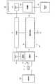
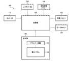
図1に本実施形態の電子機器及びこれを含む無接点電力伝送システムの基本的な構成例を示す。本実施形態の電子機器は、受電部10と回路装置90とシステムデバイス100と表示部150を含む。また電子機器は、電荷蓄積部92や通知デバイス160を含むことができる。この電子機器と送電装置200とにより、本実施形態の無接点電力伝送システム(非接触電力伝送システム)が実現される。この無接点電力伝送システムによれば、1次コイルL1と2次コイルL2を電磁的に結合させて、送電装置200から電子機器に対して無接点で電力を伝送し、電子機器の種々の動作を実現することが可能になる。1. 1. Basic Configuration of Circuit Device and Electronic Device FIG. 1 shows a basic configuration example of an electronic device of this embodiment and a non-contact power transmission system including the electronic device. The electronic apparatus according to the present embodiment includes a
なお、本実施形態の電子機器及び無接点電力伝送システムの構成は図1の構成には限定されず、その一部の構成要素を省略したり、他の構成要素を追加するなどの種々の変形実施が可能である。また本実施形態の電子機器としては、例えば表示部150を有するICカードが考えられるが、それ以外にも、電子棚札、ICタグ等の種々の機器を想定できる。また、以下では、無接点電力伝送を、その狭義な用語である電磁誘導と記載する。 Note that the configurations of the electronic device and the non-contact power transmission system of the present embodiment are not limited to the configuration of FIG. 1, and various modifications such as omitting some of the components or adding other components. Implementation is possible. Further, as the electronic device of the present embodiment, for example, an IC card having the
送電装置200は、1次コイルL1を駆動することで、電子機器の受電部10に対して電力を送電する。この送電装置200は、1次コイルL1を駆動する送電部や、送電部を制御する送電制御部などを含むことができる。送電装置200は、例えば後述するリーダー/ライターなどであり、電磁誘導送電台(充電器)としての機能や、電磁誘導によりデータを通信する機能などを有する。なお送電装置200は、送電側の電子機器に組み込まれるものであってもよい。 The
送電装置200は通知デバイス220を有する。この通知デバイス220は、蓄電の終了をユーザーに知らせるデバイスである。具体的には通知デバイス220は、表示部150の表示書き換えに必要な電荷量が、電子機器の電荷蓄積部92に蓄積されたと判断された場合に、蓄電の終了をユーザーに通知する。この通知デバイス220は、例えばスピーカーなどの音出力デバイスや、LED等の表示器などにより実現できる。 The
受電部10は、送電装置200(電磁誘導送電台、端末装置、充電器、相手側機器)から送電される電力を電磁誘導(無接点電力伝送)により受電する。例えば、金属部分の接点がなくても電力伝送を可能にする無接点電力伝送(非接触電力伝送)により電力を受電する。具体的には、送電側に設けられた1次コイルL1と、受電側に設けられた2次コイルL2を電磁的に結合させて電力伝送トランスを形成することで、非接触での電力伝送(無接点電力伝送)が実現される。この受電部10は、2次コイルL2の交流の誘起電圧を直流電圧に変換する。この変換は受電部10が有する整流回路などにより実現できる。 The
なお、1次コイルL1、2次コイルL2としては、例えば平面コイルなどを採用できるが、本実施形態はこれに限定されず、1次コイルL1と2次コイルL2を電磁的に結合させて電力を伝送できるものであれば、その形状・構造等は問わない。また、1次コイルL1(送電コイル、1次インダクター)とコイル駆動回路により送電側の回路が構成され、2次コイルL2(受電コイル、2次インダクター)とキャパシターCBとにより受電側の共振回路が構成される。 As the primary coil L1 and the secondary coil L2, for example, a planar coil can be adopted, but this embodiment is not limited to this, and the primary coil L1 and the secondary coil L2 are electromagnetically coupled to generate power. As long as it can transmit, the shape, structure, etc. are not limited. The primary coil L1 (power transmission coil, primary inductor) and a coil drive circuit constitute a power transmission side circuit, and the secondary coil L2 (power reception coil, secondary inductor) and the capacitor CB form a power reception side resonance circuit. Composed.
受電部10は、相手側機器である送電装置200との間での通信処理(RF処理)も行う。具体的には、コイルL1、L2を用いた振幅変調処理(ASK変調)により、送電装置200との間で情報の送受信を行う。或いは周波数変調処理や負荷変調処理などにより情報の送受信を行ってもよい。なお、データ通信は、電磁誘導用の1次コイルL1、2次コイルL2を用いて実現する。但し通信用の別コイルを設けて実現する変形実施も可能である。 The
回路装置90は、電荷蓄積部92への電荷蓄積の制御処理などを行う。この回路装置90は例えばASICなどにより実現できる。システムデバイス100は、電子機器のシステムとしての処理を実行するデバイスであり、例えばマイコン等の処理装置(プロセッサー)により実現できる。回路装置90、システムデバイス100の詳細については後述する。 The
表示部150は、種々の画像を表示するためのものである。システムデバイス100は、この表示部150の表示制御処理を行う。表示部150としては、例えば電気泳動表示部(以下、適宜、EPDと呼ぶ)などを採用することができ、システムデバイス100は、このEPDの表示制御処理を行う。 The
表示部150の表示情報としては、通信による受信データの情報、センサー検出情報(圧力、温度、湿度等の情報)、ICカード内蔵のメモリーの固有情報・個人情報などが考えられる。 Examples of display information on the
電子機器は通知デバイス160を有する。この通知デバイス160は、蓄電の終了をユーザーに知らせるデバイスである。具体的には通知デバイス160は、表示部150の表示書き換えに必要な電荷量が、電荷蓄積部92に蓄積されたと判断された場合に、蓄電の終了をユーザーに通知する。また、必要な電荷量が蓄積されなかった場合に、通知デバイス160がユーザーに通知し、蓄積された場合は、通知しない、若しくは、蓄積されなかった場合と違う方式で通知してもよい。この通知デバイス160は、例えばLED等の表示器や音出力デバイスなどにより実現できる。 The electronic device has a
図2は、電子機器がICカード190である場合の適用例である。ICカード190には、EPD等で実現される表示部150が設けられており、各種情報が表示可能になっている。またICカード190には、受電部10、回路装置90(IC)、後述するキャパシターC1、C2等がその内部に実装されている。 FIG. 2 shows an application example when the electronic device is an
そしてユーザーが、端末装置202(送電装置)にICカード190をかざすと、ICカード190は端末装置202からの電力を電磁誘導により受電して動作し、端末装置202とデータ通信を行う。そして、通信結果に応じた数字、文字等の画像が表示部150に表示される。電子マネーやプリペイカードを例にとれば、使用金額や残高等が表示部150に表示される。また端末装置202の表示部210にも各種情報が表示される。 When the user holds the
さて、このようなEPD等の表示部150を有するICカード190では、図1の電荷蓄積部92に蓄積した電荷に基づく電力で、表示部150の表示書き換えを実行することになる。即ち、図2のように端末装置202にICカード190をタッチする操作が行われる毎に、表示部150に表示される使用金額や残高等の表示内容を書き換える。 In the
しかしながら、図2のICカード190のタッチ操作により、端末装置202とICカード190が接近している期間は、非常に短い。そしてICカード190は、この短時間の接近期間の間に、図1のコイルL1、L2による無接点電力伝送で電力を受電して、キャパシター等により実現される電荷蓄積部92に電荷を蓄積することになる。この場合に、電荷蓄積部92には、表示部150の表示書き換えに必要な電荷量を蓄積することになり、このような電荷量を、タッチ操作の短時間の間で、電荷蓄積部92に蓄積することは容易ではない。 However, the period during which the
このため、電荷蓄積部92への蓄積電荷量が不足して、表示部150の表示書き換えが正常に完了しないなどの事態が生じる。即ち、電荷蓄積部92への蓄積電荷量が、表示部150の表示書き換えに必要な電荷量に満たない場合には、表示部150の表示が適正な表示にならなくなり、表示異常となる。そして表示部150が表示異常になると、表示結果と内部データとの間に食い違いが生じてしまう。例えば表示部150に表示される使用金額や残高と、ICカード190の内部データとして記憶される使用金額や残高との間に、食い違いが生じると、ユーザーの利便性を著しく損ねることになり、信頼性等の観点において問題があるという課題がある。 For this reason, the amount of charges stored in the
そこで、このような課題を解決するために、本実施形態では、図1に示す構成の電子機器を採用している。この電子機器は、受電部10と回路装置90とシステムデバイス100と表示部150を含む。そして、表示部150の少なくとも1回分の表示書き換えに必要な電荷が、電荷蓄積部92に蓄積されたことを条件に、表示部150の表示書き換えを行う手法により、上記課題を解決している。 Therefore, in order to solve such a problem, the electronic apparatus having the configuration shown in FIG. 1 is employed in the present embodiment. The electronic device includes a
具体的には図1の受電部10は、送電装置200から電磁誘導により電力を受電する。即ちコイルL1、L2を用いた無接点電力伝送により電力を受電する。そして回路装置90は、受電部10からの電力を受けて、電荷蓄積部92に対して電荷を蓄積する制御を行う。例えば電荷蓄積部92への充電電流の制御等を行って、電荷蓄積部92に対して電荷を蓄積する。 Specifically, the
また表示部150は、送電装置200から受電部10を介したデータ通信により受信した表示データに基づいて、画像を表示する。例えば後述するように、コイルL1、L2を用いた振幅変調等により、送電装置200と受電部10との間でのデータ通信(RF通信)が行われ、このデータ通信により受信した表示データに基づいて、図2で説明した各種の情報の画像が表示部150に表示される。電子マネーやプリペイカードを例にとれば、使用金額や残高等が表示される。この場合に、この表示部150の表示制御は、システムデバイス100(処理装置)が行う。このシステムデバイス100は、例えば表示コントローラー内蔵のマイコン等により実現される。 Further, the
そして、回路装置90(電荷蓄積制御部)は、電荷蓄積部92に電荷を蓄積する制御(蓄電制御)を行い、表示部150の少なくとも1回分の表示書き換えに必要な電荷量が電荷蓄積部92に蓄積されたか否かを判断する。必要な電荷量が蓄積されたか否かの判断は、例えば電荷蓄積部92の充電電圧情報を測定することなどで、実現できる。或いは、充電電流を制御しながら電荷蓄積部92への電荷蓄積を行う場合に、充電電流の積算処理などを行って、必要な電荷量が蓄積されたか否かを判断してもよい。 Then, the circuit device 90 (charge accumulation control unit) performs control (storage control) for accumulating charges in the
そしてシステムデバイス100は、少なくとも1回分の表示書き換えに必要な電荷量が電荷蓄積部92に蓄積されたことを条件に、表示部150の表示書き換え処理を行う。例えば回路装置90において、必要な電荷量が蓄積されたと判断された場合に、システムデバイス100は、データ通信により受信した表示データに基づいて、表示部150の表示書き換え処理を行う。 Then, the
ここで、少なくとも1回分の表示書き換えに必要な電荷とは、例えば受電後に1画面分の画像の表示書き換えを行う場合には、1画面分の画像データを書き換えるのに必要な電荷である。或いは、受電後に1画面の一部分の画像の表示書き換えを行う場合には、その一部分の画像データを書き換えるのに必要な電荷である。これらの電荷の量は、設計や実測により予め知ることができる。従って、例えば回路装置90は、その電荷量の設計値や実測値におけるワーストケースデータに対応する電荷を、電荷蓄積部92に蓄積する制御を行えばよい。 Here, the charge necessary for at least one display rewrite is, for example, a charge necessary for rewriting image data for one screen when performing display rewrite of an image for one screen after receiving power. Alternatively, when display rewriting of a part of one screen image is performed after power reception, the charge is necessary for rewriting part of the image data. The amount of these charges can be known in advance by design or actual measurement. Therefore, for example, the
またシステムデバイス100は、上述の必要電荷量(少なくとも1回分の表示書き換えに必要な電荷量)が電荷蓄積部92に蓄積されたと判断された場合に、送電装置200に対して蓄電の終了を通知する蓄電終了通知処理を行う。例えばコイルL1、L2を用いた振幅変調処理等により、蓄電の終了を知らせる通知情報を、受電部10を介して送電装置200に対して送信する。 Further, the
このようにすることで、送電装置200は、例えば通知デバイス220を用いて、蓄電が正常に終了したことをユーザーに知らせることが可能になる。具体的には、通知デバイス200は、上述の必要電荷量が電荷蓄積部92に蓄積されたと判断された場合に、蓄電の終了をユーザーに通知するデバイスであり、例えばスピーカーやLED等により実現されるデバイスである。そして、電子機器からの通知情報に基づいて、蓄電が正常に終了したことが通知された場合には、例えばスピーカーである通知デバイス220が、「ピッ」というような音を出力することで、蓄電の終了をユーザーに知らせる。 In this way, the
この場合にシステムデバイス100は、上述の必要電荷量が電荷蓄積部92に蓄積されたと判断され、且つ、送電装置200との表示データのデータ通信が終了した場合に、蓄電終了通知処理を行ってもよい。即ち、蓄電が終了したことに加えて、表示データのデータ通信が正常に終了して、表示データを適正に受信できた場合に、蓄電終了通知処理を行って、送電装置200に通知する。こうすることで、蓄電が正常に行われて、正しい表示データが表示部150に表示されるような場合に、通知デバイス220によりユーザーに通知されるようになる。 In this case, when the
なお、この通知は、電子機器に設けられた通知デバイス160により行うようにしてもよい。即ち図1の通知デバイス160は、上述の必要電荷量が電荷蓄積部92に蓄積されたと判断された場合に、蓄電の終了をユーザーに通知する。この場合に、上述と同様に、蓄電が終了し、且つ、データ通信が正常に終了した場合に、通知デバイス160によりユーザーに通知するようにしてもよい。また、必要な電荷量が蓄積されなかった場合に、通知デバイス160がユーザーに通知し、蓄積された場合は、通知しない、若しくは、蓄積されなかった場合と違う方式で通知してもよい。 This notification may be performed by the
例えば、このような通知を電子機器にて行う場合に、表示部150を用いて通知する手法も考えられる。しかしながら、必要電荷量が電荷蓄積部92に蓄積されていない場合には、表示部150の表示内容には信頼性がない。従って、表示部150とは別に、LED等で実現される通知デバイス160を設ければ、このような場合にもユーザーに対して適正な通知を行うことが可能になる。 For example, a method of notifying using the
また後述するように、回路装置90は、送電装置200との受電部10を介したデータ通信の期間において、電荷蓄積部92への電荷蓄積を制限又は停止する制御を行う。こうすることで、電荷蓄積部92の蓄電の消費電力が原因となって、データ通信に通信障害等が発生する事態を、効果的に抑制できる。 As will be described later, the
また回路装置90は、受電部10による受電終了後の期間に、電荷蓄積部92の蓄積電荷に基づく電源を、システムデバイス100に対して供給する。このようにすれば、図2に示すようなタッチ操作の間の短時間に、電荷蓄積部92に電荷を蓄積し、ICカード190が端末装置202から離れて受電が終了した後に、蓄積電荷に基づく電源をシステムデバイス100に供給して、表示部190の表示書き換え処理を実行できるようになる。 In addition, the
図3は本実施形態の手法を説明する動作フロー図である。まず、送電装置200が送電を開始すると(S61)、受電部10が受電して(S71)、回路装置90が、受電した電力に基づく電源をシステムデバイス100に供給する(S81)。これによりシステムデバイス100が起動し(S91)、表示部150も起動する(S101)。 FIG. 3 is an operation flowchart for explaining the method of the present embodiment. First, when the
次に回路装置90は、受電部10から受電した電力に基づいて、電荷蓄積部92(キャパシター)に電荷を蓄積する蓄電動作を開始する(S82)。 Next, the
一方、回路装置90からの電源供給により起動したシステムデバイス100は、送電装置200との受電部10を介したデータ通信を開始する(S92)。このデータ通信は、図1のシステムデバイス100(ホストI/F)と受電部10(ホストI/F)との間のデータ通信(S92、S72)と、後述の図5(A)で説明する受電部10と送電装置200との間のRF通信(S72、S62)とにより実現される。RF通信は、電磁誘導による無線通信である。このデータ通信により、表示部150に画像を表示するための表示データが通信される。 On the other hand, the
そして本実施形態では、電荷蓄積部92に電荷を蓄積する制御が行われ(S82)、表示部150の少なくとも1回分の表示書き換えに必要な電荷量が電荷蓄積部92に蓄積されたか否が判断される(S83)。そして、必要な電荷が蓄積され、蓄電が終了されたと判断されると、回路装置90は、蓄電の終了をシステムデバイス100に対して通知する(S84)。 In this embodiment, control for accumulating charges in the
すると、システムデバイス100は、蓄電終了の通知処理を行う(S93)。具体的には、システムデバイス100と受電部10との間のホスト通信や受電部10と送電装置200との間のRF通信により、送電装置200に対して通知する(S73、S63)。この際に、システムデバイス100は、例えば、蓄電の終了のみならず、データ通信の終了についても、送電装置200に対して通知する。 Then, the
そして送電装置200は、蓄電終了の通知を受けると、蓄電やデータ通信が正常に終了したことを通知デバイス220を用いてユーザー通知する(S64)。具体的には、スピーカー等の通知デバイス220を用いて、例えば「ピッ」というような音を出力することで、終了の通知を行う。或いは、LED等を光らせることで終了の通知を行ってもよい。そして送電装置200は、このように蓄電やデータ通信が適正に終了した場合に、電磁誘導による送電を停止する(S65)。 When the
一方、回路装置90は、蓄電の終了後、電荷蓄積部92の蓄積電力による給電をシステムデバイス100に対して行う(S85)。即ち電荷蓄積部92の蓄積電荷に基づく電源をシステムデバイス100に対して供給する。これにより、送電装置200の送電停止(S65)の後においても、システムデバイス100は、電荷蓄積部92の蓄積電荷に基づく電源により動作できるようになる。そしてシステムデバイス100は、この蓄積電荷による電源に基づいて動作して、表示部150の表示書き換え処理を実行する(S94)。これにより、表示部150には、データ通信により受信した表示データに基づく画像が表示されるようになる(S102)。 On the other hand, the
以上のように本実施形態の電子機器によれば、表示部150の少なくとも1回分の表示書き換えに必要な電荷を、電荷蓄積部92に蓄積する制御が行われ(S82)、この必要な電荷量が、電荷蓄積部92に蓄積されたか否かが判断される(S83)。そして、この必要な電荷量が電荷蓄積部92に蓄積されたことを条件に、表示部150の表示書き換え処理が行われる(S94)。 As described above, according to the electronic apparatus of the present embodiment, control is performed to store the charge necessary for at least one display rewriting of the
このようにすれば、表示書き換えに必要な電荷(適正電荷量)が電荷蓄積部92に蓄積されない限り、表示部150の表示書き換え処理は行われないようになる。従って、必要な電荷量が電荷蓄積部92に蓄積されていない状態で、表示部150の表示書き換えが行われてしまい、表示部150が表示異常になってしまうような事態の発生を抑制できる。また、表示結果と電子機器の内部データとの間に食い違いが生じて、ユーザーの利便性や信頼性を損ねるような事態の発生も抑制できる。従って、ユーザーの利便性や信頼性を向上できる電子機器を提供できる。 In this way, the display rewriting process of the
特に、図2のように短時間のタッチ操作で電力の受電とデータ通信を行う必要があるICカード190では、この短時間の期間では、必要な電荷量を電荷蓄積部92に蓄積できない事態が生じやすい。 In particular, in an
この点、本実施形態によれば、このように電力の受電期間が短時間であるICカード190においても、必要な電荷が蓄積されない限り、ICカード190の表示部150の表示書き換えが行われないことを保証できる。従って、誤った使用金額や残高がICカード190に表示されたり、ICカード190の内部データとしての使用金額や残高と、ICカード190の使用金額や残高の表示内容とが食い違ってしまうような事態の発生を抑制できる。従って、利便性が高く信頼性の高いICカード190の提供が可能になる。 In this regard, according to the present embodiment, even in the
また本実施形態の電子機器によれば、表示書き換えに必要な電荷量が電荷蓄積部92に蓄積されたと判断された場合に、蓄電の終了を通知する蓄電終了通知処理が行われる(S93)。具体的には、例えば必要な電荷量が電荷蓄積部92に蓄積されたと判断され、且つ、送電装置200との表示データのデータ通信が終了した場合に、蓄電終了通知処理が行われる。 Further, according to the electronic apparatus of the present embodiment, when it is determined that the charge amount necessary for display rewriting is stored in the
このようにすれば、例えば送電装置200側の通知デバイス220がユーザーに対して終了通知を行ったり(S64)、電子機器側の通知デバイス160がユーザーに対して終了通知を行うことなどが可能になる。従って、ユーザーは、通知デバイス220や通知デバイス160が出力する音や光等によって、必要な電力が蓄電されてデータ通信が適正に行われたことを確認できるようになり、利便性の高い電子機器の提供が可能になる。 In this way, for example, the
また本実施形態の電子機器によれば、受電部10による受電終了後の期間に、電荷蓄積部92の蓄積電荷に基づく電源が、システムデバイス100に対して供給される(S85)。これにより、システムデバイス100は、電荷蓄積部92の蓄積電荷に基づく電源により動作して、表示部150の表示書き換え処理を実行できるようになる(S94)。従って、図2のICカード160を例にとれば、短時間のタッチ操作の期間で電力を受電した後に、電荷蓄積部92の蓄積電荷に基づく電源により、表示部150の表示書き換え処理を行って、ICカード190の表示部160に使用金額や残高等を適正に表示できるようになる。 Further, according to the electronic apparatus of the present embodiment, the power based on the accumulated charge of the
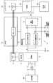
図4に、本実施形態の電子機器の回路装置90、受電部10、システムデバイス100の詳細な構成例を示す。 FIG. 4 illustrates a detailed configuration example of the
回路装置90は、電源管理部20と制御部70を含む。電源管理部20は、電源供給のための種々の管理処理(制御処理)を行う。例えば送電装置200から電磁誘導により電力を受電する受電部10からの電力を受けて、図1の電荷蓄積部92に対応するキャパシターCに対して電荷を蓄積する制御を行う。そして電源管理部20は、キャパシターCに蓄積した電荷に基づく電源を、システムデバイス100等の電源供給先デバイスに対して供給する。 The
制御部70は、本実施形態の回路装置90の種々の制御を行ったり、通信制御処理などを行う。例えば制御部70は、電磁誘導により受電部10が受電した電力により動作し、種々の制御処理を行う。具体的には、制御部70は、電荷管理部20の制御処理を行う。この制御部70は、例えばゲートアレイ回路などのデジタル回路等により実現できる。 The
受電部10は、通信部16、ホストI/F(インターフェース)18を含む。通信部16は、相手側機器である送電装置200との間での通信処理(RF処理)を行う。具体的には、コイルL1、L2を用いた振幅変調処理(ASK変調)などにより、送電装置200との間で情報の送受信を行う。ホストI/F18は、ホストとなるシステムデバイス100とのホストインターフェース処理を行う。このホストインターフェース処理は、データ線、クロック線、制御線等により実現される。 The
システムデバイス100は、ホストI/F110、処理部120を含む。ホストI/F110は、受電部10のホストI/F18との間でホスト通信処理を行う。処理部120(プロセッサー)は、表示部150の表示制御処理を行う。表示部150としては、例えば電気泳動表示部(EPD)などを採用することができ、処理部120は、このEPDの表示制御処理を行う。また処理部120は、システムの動作に必要な種々の制御処理を行う。 The
図5(A)は、送電装置200と電子機器(受電部)との間のコイルL1、L2を用いたデータ通信(RF通信)についての説明図である。図5(A)では、このデータ通信(RF通信)を、振幅変調処理により実現している。具体的には、ASK変調(振幅偏移変調:Amplitude Shift Keying)処理により実現している。ASK変調では、搬送波の振幅を入力符号(「0」、「1」)に対応させて変化させる。具体的には図5(A)では、変調で電力が途切れることがないように、ASK10%方式を採用している。なお、コマンド・データやレスポンス・データの符号化方式としては、例えばマンチェスター方式などを採用できる。また、本実施形態の近接型の無線通信方式としては、ISO/IEC1443規格のTypeA方式やTypeB方式なども想定できる。 FIG. 5A is an explanatory diagram of data communication (RF communication) using the coils L1 and L2 between the
さて、送電装置200との間で図5(A)に示すようなデータ通信を行っている際に、例えば図4の電源管理部20がキャパシターC(広義には電荷蓄積部。以下、同様)への蓄電(電荷蓄積)を行うと、この蓄電により、送電装置200から受電した電力が消費されてしまう。これにより、図5(B)に示すように、コイル端電圧信号(L1、L2)の振幅が小さくなってしまい、図5(A)のデータ通信において通信障害が生じるおそれがある。即ち、コイル端電圧信号の振幅が、図5(B)のようにキャパシターCへの蓄電が原因で小さくなると、送電装置200が図5(A)のような振幅変調を行ってデータを送信しても、受電部10がそのデータを検出できなくなってしまい、データの受信エラーが発生する。受電部10から送電装置200への送信データについても同様である。 Now, when data communication as shown in FIG. 5A is performed with the
このような問題を解決するために、本実施形態では、データ通信の期間において、電荷蓄積部へ電荷蓄積を制限又は停止する手法を採用している。 In order to solve such a problem, the present embodiment employs a technique of limiting or stopping charge accumulation in the charge accumulation unit during the data communication period.
具体的には、制御部70(回路装置90)は、送電装置200との受電部10を介したデータ通信の期間において、電源管理部20によるキャパシターC(電荷蓄積部)への電荷蓄積(以下、適宜、「蓄電」と呼ぶ)を制限又は停止する制御を行う。例えば、後述するキャパシターC1(第1の電荷蓄積部)への電荷蓄積を制限又は停止する制御を行う。 Specifically, the control unit 70 (circuit device 90) accumulates charges in the capacitor C (charge accumulation unit) by the
これらの電荷蓄積の制限又は停止は、制御部70が電源管理部20に対して制御信号を出力し、この制御信号に基づいて、キャパシターC(C1)への充電電流を制御することで実現できる。例えば電荷蓄積の制限は、充電電流を減少させることで実現できる。例えば、データ通信期間では、データ通信期間以外の期間に比べて、充電電流を減少させる。また電荷蓄積の停止は、充電電流をゼロにすることで実現できる。 The restriction or stop of the charge accumulation can be realized by the
そして電源管理部20は、受電部10による受電終了後の期間に、キャパシターC(電荷蓄積部)の蓄積電荷に基づく電源を、電源供給先デバイスに対して供給する。具体的には、電源供給先デバイスであるシステムデバイス100や表示部150に供給する。このようにすれば、受電期間が終了した後に、キャパシターCの蓄積電荷を用いてシステムデバイス100に対して電力を供給し、表示部150(EPD)の表示書き換え処理を実現できるようになる。 Then, the
なおデータ通信の期間の長さをTDCとし、キャパシターC(電荷蓄積部)に対する電荷蓄積の期間の長さをTQAとした場合に、TDC<TQAの関係が成り立つ。即ち、データ通信期間に比べて、電荷蓄積期間は十分に長い期間になる。 When the length of the data communication period is TDC and the length of the charge storage period for the capacitor C (charge storage unit) is TQA, the relationship of TDC <TQA is established. That is, the charge accumulation period is sufficiently longer than the data communication period.
また制御部70は、送電装置200とのデータ通信が終了したと判断した場合に、キャパシターC(電荷蓄積部)への電荷蓄積の制限又は停止を解除する制御を行う。例えばキャパシターCへの充電電流を制限して絞っていた場合には、これを元に戻す。またキャパシターCへの充電電流をゼロにして充電を停止していた場合には、充電電流の供給を再開する。 In addition, when it is determined that the data communication with the
以上のように本実施形態では、データ通信期間においてキャパシターCへの電荷蓄積である蓄電を制限又は停止している。即ち、データ通信が開始してから終了するまでの期間において、キャパシターCへの蓄電を制限又は停止する。 As described above, in the present embodiment, power storage, which is charge accumulation in the capacitor C, is limited or stopped during the data communication period. That is, the power storage in the capacitor C is limited or stopped during the period from the start to the end of data communication.
このようにすれば、キャパシターCへの蓄電により受電部10が受電した電力が消費されてしまい、データ通信に通信障害が発生してしまう事態を、効果的に防止できる。 In this way, it is possible to effectively prevent a situation in which the power received by the
即ち、図5(B)では、データ通信期間においてもキャパシターCへの蓄電は継続して行われているため、この蓄電による電力消費が原因で、コイル端電圧信号の振幅が低下してしまい、図5(A)のデータ通信に通信障害が発生してしまう。 That is, in FIG. 5B, since the power storage to the capacitor C is continuously performed even during the data communication period, the amplitude of the coil end voltage signal decreases due to the power consumption by the power storage, A communication failure occurs in the data communication in FIG.
この点、本実施形態の手法によれば、データ通信期間においてキャパシターCへの蓄電が制限又は停止される。従って、データ通信期間においても、コイル端電圧信号の振幅が維持されるため、通信障害が防止され、図5(A)のようなRF通信によるデータ通信を適正に実行できるようになる。従って、例えばICカードに適用した場合には、表示データの通信障害が原因となって、表示部190に画像を表示できなくなったり、或いは、誤った画像が表示されてしまうなどの事態を効果的に抑制できる。 In this regard, according to the method of the present embodiment, power storage in the capacitor C is limited or stopped during the data communication period. Accordingly, since the amplitude of the coil end voltage signal is maintained even during the data communication period, communication failure is prevented, and data communication by RF communication as shown in FIG. 5A can be executed properly. Therefore, for example, when applied to an IC card, it is effective to prevent a situation in which an image cannot be displayed on the
2.詳細な動作
次に本実施形態の詳細な動作について説明する。図6は、図2の端末装置202(送電装置)であるリーダー/ライターのポーリング動作について説明図である。2. Detailed Operation Next, a detailed operation of the present embodiment will be described. FIG. 6 is an explanatory diagram of the polling operation of the reader / writer which is the terminal device 202 (power transmission device) in FIG.
図6に示すようにリーダー/ライターは期間TAごとに間欠的に電力を送電するポーリング動作を行う。即ち、リーダー/ライターは図6のポーリング期間TPにおいて仮送電を行い、それ以外の期間では送電を停止する。そして、このポーリング期間TPにおいて、ICカード190(広義には電子機器)によるタッチ操作が行われていると、ICカード190は電力を受電し、受電した電力に基づき動作して、リーダー/ライターに対して応答を返すことになる。 As shown in FIG. 6, the reader / writer performs a polling operation for intermittently transmitting power every period TA. That is, the reader / writer performs temporary power transmission during the polling period TP in FIG. 6 and stops power transmission during other periods. If a touch operation is performed by the IC card 190 (electronic device in a broad sense) during the polling period TP, the
例えば図6のG1でカードタッチが行われると、G2に示すようにポーリング期間TPが延長されて、リーダー/ライター(端末装置202)とICカード190との間でのデータ通信が実行される。具体的には、G3でリーダー/ライターがポーリング用の電磁誘導を開始すると、G4に示すようにICカード190の電源が起動されて、G5に示すように初期通信処理が行われる。即ち初期化パラメーターの通信処理が行われる。そしてリーダー/ライターは、通信が開始したことを受信すると、G6に示すように送電の延長を行う。これによりG7に示すようなデータ通信が行われ、セキュリティー情報や各種データ(使用金額データ、残額データ等)が送受信される。更に本実施形態では、G8に示すように表示部150(EPD)の表示書き換え処理を行い、これにより、使用金額、残額等をICカード190の表示部150に表示できるようになる。 For example, when a card touch is performed at G1 in FIG. 6, the polling period TP is extended as shown at G2, and data communication between the reader / writer (terminal device 202) and the
このように、図4の制御部70は、システムデバイス100に代わって初期通信処理を行う。即ち図6のG5に示す初期通信処理は、通常はシステムデバイス100が実行するものであるが、この初期通信処理を、回路装置90に設けられた制御部70が代行する。 As described above, the
また電源管理部20は、制御部70が初期通信処理を行った後に、受電部10が受電した電力に基づく電源を、システムデバイス100に対して供給する。例えば電源管理部20は、受電部10が受電した電力に基づく電源を制御部70に供給し、これにより制御部70が起動して立ち上がり、上述の初期通信処理を行う。その後に電源管理部20からの電源がシステムデバイス100に供給されて、システムデバイス100が起動する。 The
そして初期通信が行われた後、図6のG9に示すように、ICカード190はキャパシターCへの蓄電を開始する。そしてG7に示すようにICカード190とリーダー/ライターとの間でデータ通信が行われると、本実施形態では、G10に示すようにキャパシターC(C1)への蓄電を制限又は停止する。これにより、蓄電による電力消費を原因とする電力不足により、G7に示すデータ通信に通信障害が発生する事態を防止できる。 After the initial communication is performed, the
そしてG7のデータ通信が終了すると、G11に示すようにキャパシターCへの蓄電が再開される。そして、キャパシターCに必要な電荷が蓄積されたか否かが判断され、必要な電荷が蓄積されたと判断されると、G12に示すように蓄電が終了する。そしてG13に示すように、ICカード190は、蓄電の終了をリーダー/ライターに通知する。リーダー/ライターは、G14に示すように蓄電の終了通知を受信すると、G15に示すようにICカード190への送電を停止する。 Then, when the data communication of G7 is completed, the power storage in the capacitor C is resumed as indicated by G11. Then, it is determined whether or not the necessary charge has been accumulated in the capacitor C. When it is determined that the necessary charge has been accumulated, the power storage is terminated as indicated by G12. Then, as indicated by G13, the
なお、データ通信の期間の長さをTDCとし、キャパシターC(電荷蓄積部)に対する電荷蓄積の期間の長さをTQAとした場合に、図6に示すようにTDC<TQAの関係が成り立っている。ここでデータ通信期間の長さTDCは、G7のデータ通信が開始してから終了するまでの期間の長さに対応する。また、電荷蓄積期間の長さTQAは、G9に示すように蓄電が開始してから、G12に示すように蓄電が終了するまでの期間の長さに対応する。このTQAの期間は、蓄電が制限又は停止している期間を含んでいる。 When the length of the data communication period is TDC and the length of the charge accumulation period for the capacitor C (charge storage unit) is TQA, the relationship of TDC <TQA is established as shown in FIG. . Here, the length TDC of the data communication period corresponds to the length of the period from the start to the end of the G7 data communication. The length TQA of the charge accumulation period corresponds to the length of the period from the start of power storage as indicated by G9 to the end of power storage as indicated by G12. This period of TQA includes a period during which power storage is limited or stopped.
このように、データ通信期間の長さTDCは、電荷蓄積期間の長さTQAに比べて十分に短い。従って、本実施形態の手法のように、データ通信期間中にキャパシターC(C1)への蓄電を制限又は停止しても、電荷蓄積期間を十分に確保でき、蓄積電荷に基づいて、蓄電終了後に表示部150の表示書き換えを十分に実行することが可能になる。 Thus, the length TDC of the data communication period is sufficiently shorter than the length TQA of the charge accumulation period. Therefore, as in the method of the present embodiment, even if the storage to the capacitor C (C1) is limited or stopped during the data communication period, a sufficient charge storage period can be secured, and after the end of power storage based on the stored charge. The display rewriting of the
次に本実施形態の詳細な動作について図7の動作フロー図を用いて説明する。 Next, the detailed operation of the present embodiment will be described with reference to the operation flowchart of FIG.
まず、送電装置200(リーダー/ライター等)は、電磁誘導による電力の送電を開始し(S1)、データ通信待ち状態に移行する(S2)。すると受電部10が、その電力を受電し(S11)、受電した電力に基づく電源が供給されて回路装置90が起動する(S21)。このとき、システムデバイス100は未だ起動していない状態となっている。 First, the power transmission device 200 (reader / writer, etc.) starts power transmission by electromagnetic induction (S1), and shifts to a data communication waiting state (S2). Then, the
起動した回路装置90は、未だ起動していないシステムデバイス100に代わって、初期通信処理を実行する(S22)。具体的には初期化パラメーターの送信処理を行う。 The activated
受電部10は、ホストI/F18を介したホスト通信により初期化パラメーターを受信すると(S12)、送電装置200とのRF通信を行う(S13)。これによりステートがRF応答ステートに移行する。具体的には送電装置200がポーリングコマンドを送信し、このポーリングコマンドを受信した受電部10(通信部16)が、ポーリング応答を送電装置200に送信する。この場合のRF通信は、コイルL1、L2を用いた電磁誘導により実現される。 When receiving the initialization parameter by host communication via the host I / F 18 (S12), the
送電装置200は、受電部10からポーリング応答が返って来たかを確認して、ポーリングに成功したか否かを判断し(S3)、ポーリング応答が返って来なかった場合にはポーリングに失敗したと判断する(S4)。一方、ポーリング応答が返って来て、システムが適合したと判定される場合には、ポーリングに成功したと判断して、図6のG2、G6に示すように送電期間を延長する(S5)。そしてデータ通信待ち状態に移行する(S6)。 The
回路装置90は、初期通信処理を行った後に、システムデバイス100への給電を開始する(S23)。具体的には、受電部10からの電力を受けた電源管理部20が、この電力に基づく電源をシステムデバイス100に供給する。これによりシステムデバイス100のハードウェアが起動し(S41)、それに続いて、ハードウェア上で動作するソフトウェア(ファームウェア)が起動する(S42)。 After performing the initial communication process, the
次に、回路装置90は、電荷蓄積部であるキャパシターCへの電荷蓄積動作を開始する(S24)。これによりキャパシターCに対する電荷蓄積が行われる(S25)。 Next, the
一方、システムデバイス100は、送電装置200とのデータ通信を開始する場合には、通信準備の通知を回路装置90に対して行う(S43)。すると、この通知を受けた回路装置90は、キャパシターC(後述するC1)への蓄電を制限又は停止する。これにより、蓄電による電力消費を原因とする通信障害の発生が抑制される。 On the other hand, when starting the data communication with the
そしてシステムデバイス100は、表示データの通信処理を開始する(S44)。具体的には、システムデバイス100のホストI/F110と受電部10のホストI/F18との間で、表示データのホスト通信が行われ、受電部10(通信部16)と送電装置200との間で表示データのRF通信(コイルを用いた電磁誘導による通信)が行われる(S14、S7)。 Then, the
このデータ通信が終了すると、システムデバイス100は、通信終了を回路装置90に通知する(S45)。すると回路装置90は、S26の蓄電の制限又は停止を解除して、キャパシターC(C1)への蓄電を再開する(S27)。 When the data communication ends, the
そして回路装置90は、キャパシターCへの電荷蓄積が終了すると(S28)、蓄電の終了通知を行う(S29)。具体的には、表示部150の少なくとも1回分の表示書き換えに必要が電荷がキャパシターCに蓄積されたか否かを判断し、必要な電荷が蓄積されたと判断した場合には、システムデバイス100に対して蓄電の通知を行う。 When the charge accumulation in the capacitor C is completed (S28), the
すると、この通知を受けたシステムデバイス100は、蓄電終了の通知処理を行う(S46)。具体的には、ホスト通信、RF通信により、受電部10、送電装置200に対して、蓄電の終了を通知する処理を行う(S15、S8)。或いは、ICカード190(電子機器)が、LED等の通知デバイス160を有する場合に、この通知デバイス160を用いて、蓄電の終了をユーザに通知するための処理を行う。 Then, the
一方、システムデバイス100から、蓄電終了の通知を受信した送電装置200は、スピーカーやLED等の表示器により実現される通知デバイス220を用いて、蓄電が終了したことをユーザーに対して通知する(S9)。そしてICカードに対する送電を停止する(S10)。 On the other hand, the
一方、回路装置90は、キャパシターCへの蓄電が終了すると、蓄電電力によるシステムデバイス100への給電を行う(S30)。即ち、このときには送電装置200による送電は停止しており、受電部10の受電期間は終了している。このため回路装置90は、キャパシターCに蓄積された電荷に基づく電源を、システムデバイス100に対して供給する。すると、システムデバイス100は、キャパシターCによる供給電源に基づいて動作して、表示部150の表示書き換え処理を開始して実行する(S47、S48)。そして、キャパシターCの蓄積電荷を用いた表示書き換え処理が無事に終了すると(S49)、正常終了となる(S50)。そしてキャパシターCの蓄積電荷に基づく給電も終了する(S31)。 On the other hand, when the storage of the capacitor C is completed, the
以上のように本実施形態では、表示部150の少なくとも1回分の表示書き換えに必要な電荷量がキャパシターC(電荷蓄積部)に蓄積されたか否かが判断され(S27、S28)、この必要な電荷量が蓄積されたことを条件に、表示部150の表示書き換え処理が行われる(S48)。従って、必要な電荷量が蓄積されていないのに表示書き換え処理が行われてしまい、誤った表示が行われたり、電子機器の内部データと表示内容が食い違ってしまうような事態の発生を抑制できる。 As described above, in the present embodiment, it is determined whether or not the charge amount necessary for at least one display rewriting of the
また本実施形態によれば、必要な電荷量が蓄積されると、送電装置200に対して蓄電終了通知処理が行われる(S46)。従って、通知デバイス220等を用いて、蓄電やデータ通信の適正な終了をユーザーに知らせることができるようになり、利便性を向上できる。 Further, according to the present embodiment, when the necessary amount of charge is accumulated, a power storage end notification process is performed on the power transmission device 200 (S46). Therefore, the
また本実施形態によれば、システムデバイス100と送電装置200とのデータ通信期間(S44、S14、S7)において、キャパシターC(C1)への蓄電が制限又は停止されるため(S26)、通信障害の発生を効果的に抑制できる。そして、データ通信が終了すると、この蓄電の制限又は停止が解除されて、蓄電が再開されるため(S27)、例えば表示部150の少なくとも1回分の表示書き換えに必要な電荷をキャパシターCに対して適正に蓄積できるようになる。 Further, according to the present embodiment, in the data communication period (S44, S14, S7) between the
3.起動用キャパシター
図8に、本実施形態の電子機器の詳細な第1の構成例を示す。図8では、電源管理部20が、第1の蓄積制御部30と第2の蓄積部40と電源供給部50を含む。3. Starting Capacitor FIG. 8 shows a detailed first configuration example of the electronic apparatus of this embodiment. In FIG. 8, the
第1の蓄積制御部30(第1の蓄積動作部)は、電磁誘導により電力を受電する受電部10からの電力を受けて、蓄電用のキャパシターC1(広義には第1の電荷蓄積部)に対して電荷を蓄積する制御(動作)を行う。第2の蓄積制御部40(第2の蓄積動作部)は、受電部10からの電力を受けて、起動用のキャパシターC2(広義には第2の電荷蓄積部)に対して電荷を蓄積する制御(動作)を行う。 The first accumulation control unit 30 (first accumulation operation unit) receives power from the
具体的には、第1の蓄積制御部30は、受電部10からの電力の入力ノードNIと、第1の蓄積ノードNA1との間に設けられる。そして、蓄電用のメインのキャパシターC1を充電するための電流や電圧を制御して、キャパシターC1への充電制御を行う。 Specifically, the first
例えばシステムデバイス100が、画像を表示する電気泳動表示部(EPD)の表示制御処理を行う場合を想定する。この場合には、第1の蓄積制御部30は、電気泳動表示部(不揮発性表示素子)の少なくとも1回分の表示書き換えに必要な電荷を、キャパシターC1に蓄積する制御を行う。このようにすることで、電磁誘電による受電後に、システムデバイス100の表示部を少なくとも1回だけ書き換えることが可能になる。これにより、例えばプリペイカードや電子マネーのICカードに適用した場合には、端末装置にICカードをかざした後に、使用金額や残高等をICカードの表示部に表示することが可能になる。 For example, it is assumed that the
一方、第2の蓄積制御部40は、受電部10からの電力の入力ノードNIと、第2の蓄積ノードNA2との間に設けられる。そして、起動用のサブのキャパシターC2を充電するための電流や電圧を制御して、キャパシターC2への充電制御を行う。 On the other hand, the second
電源供給部50は、電磁誘導の電力による電源をシステムデバイス100や制御部70に対して供給する。例えば電源供給部50は、キャパシターC1、C2(第1、第2の電荷蓄積部)に蓄積された電荷に基づいて、システムデバイス100や制御部70に対して電源を供給する。具体的には、蓄積ノードNA1、NA2の電圧に基づく電源電圧を、システムデバイス100への電源の出力ノードNQに対して出力する。 The
この場合に電源供給部50は、キャパシターC2(第2の電荷蓄積部)の蓄積電荷により得られる電源電圧が、システムデバイス100の動作下限電圧を超えた後に、システムデバイス100に対して電源を供給することが望ましい。ここで、動作下限電圧は、システムデバイス100が正常な動作を行うことが保証されている電圧である。例えばシステムデバイス100がマイコン(表示コントローラー内蔵マイコン)である場合には、マイコンの仕様などにより動作下限電圧が規定される。例えば動作下限電圧よりも低い電源電圧がシステムデバイス100に供給されると、システムデバイス100を構成するトランジスターに貫通電流が流れるなどの不具合が発生するおそれがある。この点、電源供給部50が、動作下限電圧を超えるまでシステムデバイス100に対して電源を供給しないようにすることで、このような不具合の発生を防止できる。 In this case, the
そして本実施形態では、キャパシターC2(第2の電荷蓄積部)は、蓄電用のキャパシターC1(第1の電荷蓄積部)よりも電荷の蓄積容量(キャパシタンス)が小さいシステム起動用の電荷蓄積部となっている。一例としては、蓄電用のキャパシターC1の容量は、数十μF〜数百μF(例えば100μF程度)であり、起動用のキャパシターC2の容量は、1μF以下(例えば0.1μF程度)である。この蓄電素子となるキャパシターC1等としては、スーパーキャパシターなどのコンデンサーを使用できる。従って、蓄電素子を薄型に構成できるため、ICカード等にも容易に内蔵することが可能になる。 In this embodiment, the capacitor C2 (second charge storage unit) includes a system startup charge storage unit having a charge storage capacity (capacitance) smaller than that of the storage capacitor C1 (first charge storage unit). It has become. As an example, the capacity of the capacitor C1 for storing electricity is several tens of μF to several hundreds of μF (for example, about 100 μF), and the capacity of the starting capacitor C2 is 1 μF or less (for example, about 0.1 μF). A capacitor such as a supercapacitor can be used as the capacitor C1 or the like serving as the power storage element. Accordingly, since the power storage element can be configured to be thin, it can be easily built in an IC card or the like.
キャパシターC1の一端は、第1の蓄積制御部30の出力ノードである蓄積ノードNA1に接続され、他端は例えばGNDノードに接続される。またキャパシターC2の一端は、第2の蓄積制御部40の出力ノードである蓄積ノードNA2に接続され、他端は例えばGNDノードに接続される。なお、電力の入力ノードNIには、電位安定化用のキャパシターCCの一端が接続されている。 One end of the capacitor C1 is connected to the storage node NA1, which is an output node of the first
そして電源供給部50は、受電部10による受電開始後のシステム起動時には、キャパシターC2(第2の電荷蓄積部)の蓄積電荷に基づく電源を、システムデバイス100や制御部70に対して供給する。即ち、システム起動時には、システム起動用の小容量のキャパシターC2の蓄積電荷に基づく電源(ノードNA2の電圧に基づく電源電圧)を、システムデバイス100や制御部70に対して供給する。 The
そして制御部70は、キャパシターC2(第2の電荷蓄積部)の蓄積電荷に基づく電源が供給されて起動したシステムデバイス100により、送電装置200とのデータ通信の開始を通知された場合に、電源管理部20によるキャパシターC1(第1の電荷蓄積部)への電荷蓄積を、制限又は停止する制御を行う。例えば図7のS43の通知がシステムデバイス100から来た場合に、キャパシターC1(第1の電荷蓄積部)への電荷蓄積を、制限又は停止する制御を行う。こうすることで、蓄電に大きな電力が必要なキャパシターC1への蓄電が制限又は停止されるため、蓄電電力が原因となってデータ通信に通信障害が発生する事態を、効果的に抑制できるようになる。 Then, when the
一方、電源供給部50は、受電部10による受電終了後の期間においては、キャパシターC1(第1の電荷蓄積部)の蓄積電荷に基づく電源を、システムデバイス100や制御部70に対して供給する。即ち、システムが起動してキャパシターが十分に充電された受電終了後の期間においては、蓄電用の大容量のキャパシターC1の蓄積電荷に基づく電源(ノードNA1の電圧に基づく電源電圧)を、システムデバイス100や制御部70に対して供給する。 On the other hand, the
なお、受電終了後の期間にシステムデバイス100や制御部70に供給される電源は、キャパシターC1、C2の両方の蓄積電荷に基づく電源であることが望ましい。また、キャパシターC2の蓄積電荷に基づく電源は、受電期間のうちシステム起動時(受電期間の前半)にシステムデバイス100や制御部70に供給されれば十分であり、例えば受電期間の後半において、キャパシターC1の蓄積電荷に基づく電源がシステムデバイス100や制御部70に供給されてもよい。 Note that the power supplied to the
以上の図8に示す第1の構成例では、受電部10による受電開始後に、起動用の小容量のキャパシターC2は短時間で充電されるため、システムデバイス100や制御部70に対して迅速に電源電圧を供給してシステムを立ち上げることが可能になる。そして、その後に、キャパシターC2よりも大容量の蓄電用のキャパシターC1が充電され、受電期間終了後も、このキャパシターC1に充電された電荷に基づいて、システムデバイス100や制御部70に電源を供給して動作させることが可能になる。 In the first configuration example shown in FIG. 8 described above, since the small-capacitance capacitor C2 for activation is charged in a short time after the power reception by the
例えば非接触のICカードに本実施形態の回路装置を適用する場合、短い時間で端末装置と通信を行い、蓄電する必要がある。ところが、蓄電されるキャパシターは大容量であり、その充電電圧の立ち上がりは遅く、システム(システムデバイス)のリセットが解除されずに、通信を開始できないという課題がある。 For example, when the circuit device according to the present embodiment is applied to a non-contact IC card, it is necessary to communicate with the terminal device in a short time to store electricity. However, the stored capacitor has a large capacity, and the rising of the charging voltage is slow, and there is a problem that communication cannot be started without releasing the reset of the system (system device).
この点、本実施形態では図8に示すように、蓄電用の大容量のキャパシターC1に加えて、起動用の小容量のキャパシターC2が設けられている。これにより、受電開始の直後は、このキャパシターC2の充電電圧でシステムデバイス100や制御部70を動作させて通信等を行うことが可能になる。従って、蓄電用のキャパシターC1の容量に依存せずに、システムを立ち上げることができ、通信システムを早期に立ち上げて、蓄電及び通信時間を短くすることが可能になる。 In this regard, in this embodiment, as shown in FIG. 8, in addition to the large-capacity capacitor C1 for power storage, a small-capacitance capacitor C2 for activation is provided. As a result, immediately after the start of power reception, the
例えば、不揮発表示素子であるEPDは、表示情報を無電源状態で保持できるため、ICカード190の表示部150として好適な表示装置である。 For example, an EPD that is a non-volatile display element is a display device suitable as the
ところが、EPDは、液晶表示装置に比べて、表示情報の書き換えに長時間(例えば1秒)を要するという問題点がある。このため、端末装置202にICカード190をかざすというタッチ&ゴー(Touch&Go)の操作で、電力を受電して、EPDの表示書き換えを行うのは困難であるという課題がある。 However, EPD has a problem that it takes a long time (for example, 1 second) to rewrite display information as compared with a liquid crystal display device. For this reason, there is a problem that it is difficult to receive power and rewrite the display of the EPD by touch & go operation of holding the
例えば図9(A)の比較例の手法では、電磁誘導による受電期間TRの長さT1を長くし、A1に示すように受電期間TRの前半において、端末装置202(リーダー/ライター)からのデータ受信を行う。そして、A2に示すように受電期間TRの後半のシステムデバイス100の動作期間において、EPDの表示書き換えを行っている。この場合、システムデバイス100の動作期間の長さT2は、受電期間TRの長さT1よりも短くなる。 For example, in the method of the comparative example of FIG. 9A, the length T1 of the power reception period TR due to electromagnetic induction is lengthened, and data from the terminal device 202 (reader / writer) in the first half of the power reception period TR as indicated by A1. Receive. Then, as shown at A2, the display rewriting of the EPD is performed in the operation period of the
しかしながら、図9(A)の比較例の手法では、受電期間TRの長さT1が長くなってしまうため、タッチ&ゴーの操作(例えば0.1秒程度の長さの操作)を実現できなくなってしまう。 However, in the method of the comparative example in FIG. 9A, since the length T1 of the power reception period TR is increased, it becomes impossible to realize a touch and go operation (for example, an operation having a length of about 0.1 seconds). End up.
そこで本実施形態では、図9(B)に示すように、受電期間TRの長さT1を短くする。そしてA3に示すように受電期間TRの間に、端末装置202からのデータ受信を行い、A4に示すように、その後のシステムデバイス100の動作期間においてEPDの表示書き換えを行う。この場合に、受電期間TRの長さをT1とし、システムデバイス100の動作期間の長さをT2とした場合に、T2>T1の関係が成り立つようにする。 Therefore, in the present embodiment, as shown in FIG. 9B, the length T1 of the power reception period TR is shortened. Then, data reception from the
このように、受電期間TRの長さT1を短くすることで、タッチ&ゴーの操作で、ICカード190が電力を受電して動作することが可能になる。また、システムデバイス100の動作期間の長さT2が長いことで、表示部150としてEPDを利用した場合にも、表示情報の書き換えが可能になる。即ち、EPDは、液晶表示装置に比べて、表示情報の書き換えに長時間(1秒)を要するが、T2の期間は、データ受信期間と少なくとも1回分のEPDの表示書き換えに必要な時間とする。 Thus, by shortening the length T1 of the power reception period TR, the
この場合に、受電期間TRの長さT1が短いと、EPDの表示書き換えに必要な十分な電荷を蓄積できないおそれがある。 In this case, if the length T1 of the power reception period TR is short, there is a possibility that sufficient electric charge necessary for EPD display rewriting cannot be accumulated.
そこで図8では、蓄電用のキャパシターC1として大容量のキャパシターを設けている。例えばキャパシターC1として、スーパーキャパシターなどのコンデンサーを用いることで、EPDの表示書き換えに必要な十分な電荷を蓄積することが可能になる。 Therefore, in FIG. 8, a large-capacity capacitor is provided as the capacitor C1 for power storage. For example, by using a capacitor such as a supercapacitor as the capacitor C1, it is possible to accumulate sufficient electric charge necessary for display rewriting of the EPD.
一方、このように蓄電用のキャパシターC1を大容量にすると、システムデバイス100に供給される電源電圧が、なかなか立ち上がらずに、早期にシステムを起動できなくなってしまうという課題がある。 On the other hand, when the capacitor C1 for power storage has a large capacity as described above, there is a problem that the power supply voltage supplied to the
そこで本実施形態では、蓄電用のキャパシターC1とは別に起動用のキャパシターC2を設けている。つまり、図9(A)の比較例では、蓄電用キャパシターのみで蓄電及びシステムの起動を行っている。これに対して本実施形態では、蓄電時間を短縮するために、比較例に比べて大容量の蓄電用キャパシターC1を用い、且つ起動を早くするために起動用キャパシターC2を更に別に設けている。 Therefore, in the present embodiment, a startup capacitor C2 is provided separately from the storage capacitor C1. That is, in the comparative example of FIG. 9A, power storage and system startup are performed using only the power storage capacitor. On the other hand, in the present embodiment, in order to shorten the storage time, a storage capacitor C1 having a larger capacity than that of the comparative example is used, and a startup capacitor C2 is further provided in order to speed up the startup.
そして図10(A)のB1、B2に示すように、これらのキャパシターC1、C2は、受電部10からの出力電圧に基づいて、第1、第2の蓄積制御部30、40を介して充電される。 Then, as shown in B1 and B2 of FIG. 10A, these capacitors C1 and C2 are charged via the first and second
そして図10(A)のB3に示すように、受電部10による受電開始後のシステム起動時には、起動用のキャパシターC2の蓄積電荷に基づく電源が、システムデバイス100に対して供給される。即ち、起動用のキャパシターC2の容量は小さいため、C2の電荷蓄積ノードNA2の電圧の立ち上がりは早く、この電圧がB3に示すように電源電圧としてシステムデバイス100に供給される。 Then, as indicated by B <b> 3 in FIG. 10A, power is supplied to the
一方、図10(B)に示すように、受電部10による受電終了後の期間では、蓄電用のキャパシターC1の蓄積電荷に基づく電源が、システムデバイス100に対して供給される。即ち、蓄電用のキャパシターC1の容量は大きいため、C1の電荷蓄積ノードNA1の電圧の立ち上がりは遅い。しかしながら、受電開始後、時間が経過すると、この電圧は、システムデバイス100の動作下限電圧を上回るようになり、B4に示すように電源電圧としてシステムデバイス100に供給できるようになる。 On the other hand, as shown in FIG. 10B, in the period after the end of power reception by the
こうすることで、図9(B)のA5に示すように早期にシステム電源をオンにしてシステムデバイス100を動作させることが可能になる。これにより、A3に示すデータ受信処理を早期に完了させることが可能になり、タッチ&ゴーの操作を実現する短い受電期間にも対応できるようになる。 By doing so, it becomes possible to operate the
また本実施形態では、図8のように起動用のキャパシターC2を設けることで、制御部70に供給する電源についても早期に立ち上げることが可能になる。例えばノードNA2の電圧が早期に立ち上がることで、このノードNA2の電圧に基づく電源を制御部70に供給して、制御部70を早期に動作させることが可能になる。これにより図7のS22の初期通信処理が早期に行われるようになり、ポーリング期間内での応答を迅速に行うことが可能になる。なお、制御部70はホストI/F71を有している。そして、初期通信処理は、制御部70のホストI/F71が、システムデバイス100のホストI/F110に代わって、受電部10のホストI/F18に対して初期化パラメーターを送信することにより実現される。 Further, in the present embodiment, by providing the start-up capacitor C2 as shown in FIG. 8, it is possible to start up the power supplied to the
また本実施形態では、データ通信期間においては、このような大容量で大きな蓄電電力が必要なキャパシターC1への蓄電が制限又は停止される。従って、キャパシターC1への蓄電電力を原因として、コイル端電圧信号の振幅が小さくなって、データ通信の通信障害が発生してしまう事態を、効果的に抑制できる。 Further, in the present embodiment, during the data communication period, the power storage to the capacitor C1 that requires such a large capacity and a large amount of stored power is limited or stopped. Therefore, it is possible to effectively suppress a situation in which a communication failure in data communication occurs due to a decrease in the amplitude of the coil end voltage signal due to the stored power in the capacitor C1.
そして、このように、データ通信期間中にキャパシターC1への蓄電を制限又は停止したとしても、キャパシターC2の蓄積電荷に基づく電源を、システムデバイス100や制御部70に供給できる。例えば図10(A)のB2、B3に示すような経路で電源を供給できる。従って、システムデバイス100や制御部70は、このキャパシターC2の蓄積電荷に基づく電源によって動作して、データ通信等の各処理を適正に実行することが可能になる。この場合に、キャパシターC2は小容量であるため、キャパシターC2の蓄電により消費される電力は最小限で済むため、データ通信の通信障害も防止できる。 As described above, even if power storage in the capacitor C1 is restricted or stopped during the data communication period, the power based on the accumulated charge in the capacitor C2 can be supplied to the
4.電流制御
図11に、本実施形態の電子機器の詳細な第2の構成例を示す。なお図8の第1の構成例と同様の部分については、同様の符号を付して、詳細な説明を省略する。4). Current Control FIG. 11 shows a detailed second configuration example of the electronic apparatus of the present embodiment. In addition, about the part similar to the 1st structural example of FIG. 8, the same code | symbol is attached | subjected and detailed description is abbreviate | omitted.
図11の第2の構成例では、電源管理部20が電流制御部32を含む。具体的には、電源管理部20の第1の蓄積制御部30が電流制御部32を含む。この電流制御部32は、制御部70の制御に基づいて、キャパシターC1(広義には電荷蓄積部)への充電電流を制御する。例えば電流制御部32は、電磁誘導により電力を受電する受電部10からの電力を受けて、キャパシターC1に充電電流を流す制御を行う。即ち、電流値が可変の充電電流をキャパシターC1に流す制御を行って、キャパシターC1を充電する。 In the second configuration example of FIG. 11, the
制御部70は、電流制御部32を制御して、充電電流を制御する。例えば制御部70は、充電電流の制御信号を電流制御部32に対して出力することで、充電電流の大きさ(電流値)を制御する。例えば制御部70は、電荷蓄積ノードNA1の充電電圧を測定し、測定結果に基づいて、nビットの制御信号の各ビットの信号レベルを設定することで、電流制御部32が流す充電電流の大きさを制御する。 The
そして制御部70は、キャパシターC1(電荷蓄積部)の充電電圧が高くなるほど充電電流を小さくする制御を、電流制御部32に対して行う。例えば制御部70は、充電開始時には大きな第1の電流値の充電電流でキャパシターC1を充電するように、電流制御部32を制御する。そして、充電電圧が第1の電圧値を超えた場合には、第1の電流値よりも小さな第2の電流値の充電電流でキャパシターC1を充電するように、電流制御部32を制御する。更に、充電電圧が、第1の電圧値よりも大きな第2の電圧値を超えた場合には、第2の電流値よりも小さな第3の電流値の充電電流でキャパシターC1を充電するように、電流制御部32を制御する。このように制御部70は、キャパシターC1の充電電圧(ノードNA1の電圧)が高くなるにつれて、充電電流を例えば段階的に小さくする制御を行う。 Then, the
この場合に、制御部70は、送電装置200とのデータ通信の期間においては、キャパシターC1(電荷蓄積部)への充電電流を制限又は停止する制御を、電流制御部32に対して行う。これにより、図6のG10や図7のS26等で説明した、蓄電を制限又は停止する制御を実現できる。即ち、この第1の構成例では、充電電流を制御する電流制御部32の機能を有効活用して、蓄電を制限又は停止する制御を実現している。 In this case, the
なお制御部70は、キャパシターC1の充電電圧を特定する電圧情報を測定し、測定された電圧情報に基づいて充電電流の制御を行う。 In addition, the
例えば図11に示すように制御部70は、A/D変換部72、タイマー74、演算処理部76を含む。A/D変換部72(電圧情報取得部)は、キャパシターC1の充電電圧をA/D変換することで、充電電圧の電圧情報を測定(取得)する。演算処理部76は、測定された電圧情報と、タイマー74により設定される時間情報に基づいて、充電電流の値を決める演算処理を行って、充電電流の制御信号を電流制御部32に出力する。 For example, as illustrated in FIG. 11, the
更に具体的には、制御部70(演算処理部76)は、測定された電圧情報に基づいて、キャパシターC1(電荷蓄積部)の蓄積電荷量を求める。そして、求められた蓄積電荷量と、電源供給先デバイス(システムデバイス100等)を動作させるのに必要なトータル電荷量とに基づいて、ターゲット電荷量を求める。そして、キャパシターC1の蓄積電荷量が、少なくともターゲット電荷量に達するまで、キャパシターC1に充電電流を流す制御を行う。 More specifically, the control unit 70 (arithmetic processing unit 76) obtains the accumulated charge amount of the capacitor C1 (charge accumulation unit) based on the measured voltage information. Then, the target charge amount is obtained based on the obtained accumulated charge amount and the total charge amount necessary for operating the power supply destination device (
このように本実施形態によれば、A/D変換部72等により測定されたキャパシターC1の充電電圧の情報に基づいて、キャパシターC1の蓄積電荷量を求めることができる。従って、図3のS83や図7のS28において、少なくとも1回分の表示書き換えに必要な電荷量がキャパシターC1に蓄積されたか否かを判断することが可能になる。そして、この必要な電荷量が蓄積されたことを条件に、表示部150の表示書き換え処理を行うことで、誤った表示が行われたり、内部データと表示内容との間に食い違いが生じるなどの事態の発生を抑制できる。 As described above, according to the present embodiment, the accumulated charge amount of the capacitor C1 can be obtained based on the information on the charging voltage of the capacitor C1 measured by the A /
次に、図11の第2の構成例による充電手法について詳細に説明する。図12(A)は、無接点電力伝送における電圧と電流の関係を示す図である。図12(A)のVIは、受電部10の出力電圧であり、IIは出力電流である。この電圧VIは、二次コイルL2のコイル端電圧を、例えば受電部10が有する整流回路により整流することで得られる電圧(DC電圧)である。 Next, the charging method according to the second configuration example of FIG. 11 will be described in detail. FIG. 12A is a diagram illustrating the relationship between voltage and current in contactless power transmission. In FIG. 12A, VI is an output voltage of the
図12(A)に示すように、電磁誘導で受電するシステムにおいては、電流IIが小さければ高い電圧VIを確保できるが、大きな電流IIを取り出そうとすると、電圧VIが低下してしまうという特性がある。 As shown in FIG. 12A, in a system that receives power by electromagnetic induction, a high voltage VI can be secured if the current II is small, but if the large current II is extracted, the voltage VI decreases. is there.
一方、電源供給先デバイスの1つであるシステムデバイス100には、動作下限電圧が規定されている。このため、キャパシター(C1)に蓄積された電荷に基づく電源をシステムデバイス100に供給する場合には、供給される電源電圧が動作下限電圧を下回らないようにする必要がある。 On the other hand, an operating lower limit voltage is defined for the
そこで本実施形態では、受電部10の受電終了後、キャパシターの蓄積電荷に基づく電源でシステムデバイス100等を動作させる場合に、キャパシターの充電電圧が動作下限電圧を下回らないような量の電荷を、キャパシターに充電する手法を採用している。 Therefore, in the present embodiment, when the
ところが、このような手法を採用した場合に、蓄電用のキャパシターの容量が大きいと、無駄な蓄電が行われる事態が生じてしまうことが判明した。 However, when such a method is employed, it has been found that if the capacity of the power storage capacitor is large, a situation where wasteful power storage is performed occurs.
例えば図12(B)において、キャパシターの容量が大きい場合には、動作下限電圧の充電電圧を確保するために、電荷量QA1が必要になる。そして、受電後の電源供給先デバイスの動作に必要な電荷量QA2を、キャパシターに蓄電すれば、電源供給先デバイスの動作期間において、キャパシターの充電電圧を動作下限電圧以上に確保することができる。これにより、受電終了後の動作期間の間、キャパシターの蓄積電荷に基づいて電源供給先デバイスを無事に動作させることが可能になる。 For example, in FIG. 12B, when the capacitance of the capacitor is large, the charge amount QA1 is necessary to secure the charging voltage of the operation lower limit voltage. If the charge amount QA2 necessary for the operation of the power supply destination device after receiving power is stored in the capacitor, the charging voltage of the capacitor can be secured to the operation lower limit voltage or more during the operation period of the power supply destination device. As a result, the power supply destination device can be safely operated based on the accumulated charge of the capacitor during the operation period after the end of power reception.
そして、図12(B)において、キャパシターの容量が小さい場合には、動作下限電圧の充電電圧を確保するために、電荷量QB1が必要になる。そして、受電後の電源供給先デバイスの動作に必要な電荷量QB2を、キャパシターに蓄電すれば、受電終了後の動作期間の間、キャパシターの蓄積電荷に基づいて電源供給先デバイスを無事に動作させることが可能になる。 In FIG. 12B, when the capacitance of the capacitor is small, the charge amount QB1 is required to secure the charge voltage of the operation lower limit voltage. If the amount of charge QB2 necessary for the operation of the power supply destination device after receiving power is stored in the capacitor, the power supply destination device is safely operated based on the accumulated charge in the capacitor during the operation period after the end of power reception. It becomes possible.
ここで、図12(B)に示すように、動作下限電圧を確保するための電荷量については、QA1>QB1の関係が成り立つ。受電後の動作に必要な電荷量については、QA2=QB2の関係が成り立つ。そして、動作下限電圧の確保に必要な電荷量QA1、QB1は、動作時には使用されない余剰な電力になるため、この電荷量が多いと蓄電電力の無駄になる。従って、このような無駄を軽減し、蓄電の効率化を図るためには、キャパシターの容量はなるべく小さい方が望ましい。 Here, as shown in FIG. 12B, the relationship of QA1> QB1 holds for the amount of charge for securing the operation lower limit voltage. Regarding the amount of charge necessary for the operation after receiving power, the relationship of QA2 = QB2 is established. The charge amounts QA1 and QB1 necessary for securing the operation lower limit voltage become surplus power that is not used during operation. Therefore, if this charge amount is large, the stored power is wasted. Therefore, in order to reduce such waste and increase the efficiency of power storage, it is desirable that the capacity of the capacitor be as small as possible.
一方、図12(B)から明らかなように、キャパシターの容量を小さくすると、受電後の動作に必要な電荷量QB2を蓄電するために、充電電圧を高くする必要がある。即ち、無駄な蓄電電力を軽減して、蓄電の効率化を図るためには、キャパシターの容量を小さくして、充電電圧を高くする手法が望ましい。 On the other hand, as is clear from FIG. 12B, when the capacitance of the capacitor is reduced, the charge voltage needs to be increased in order to store the charge amount QB2 necessary for the operation after receiving power. That is, in order to reduce wasteful stored power and increase the efficiency of power storage, it is desirable to reduce the capacity of the capacitor and increase the charging voltage.
ところが、電磁誘導で受電するシステムにおいては、電圧VIと電流IIの間に図12(A)の関係が成り立つ。従って、キャパシターの容量を小さくした場合に、キャパシターの充電電圧を高くできなくなり、受電後の動作に必要な電荷量QB2をキャパシターに蓄電することが難しくなるという課題がある。 However, in the system that receives power by electromagnetic induction, the relationship of FIG. 12A is established between the voltage VI and the current II. Therefore, when the capacitance of the capacitor is reduced, the charging voltage of the capacitor cannot be increased, and there is a problem that it is difficult to store the charge amount QB2 necessary for the operation after receiving power in the capacitor.
このような課題を解決するために、図11の第2の構成例では、図13(A)に示すように、キャパシターの充電電圧が高くなるほど、充電電流を小さくする充電手法を採用している。 In order to solve such a problem, the second configuration example of FIG. 11 employs a charging method in which the charging current is reduced as the charging voltage of the capacitor increases, as shown in FIG. .
このようにすれば図13(B)に示すように、受電部側(コイル側)の電圧−電流特性(VI−II特性)と、キャパシター側の充電電圧−充電電流特性(VCH−ICH特性)をマッチングさせることが可能になる。従って、図12(B)に示すように、キャパシターの容量を小さくして、蓄電の効率化と動作下限電圧の確保を両立できるようになる。また、キャパシターの容量を小さくすることで、ICカード190のキャパシターの実装スペースを小さくすることが可能になり、装置の小型化にも貢献できるようになる。 If it does in this way, as shown in FIG.13 (B), the voltage-current characteristic (VI-II characteristic) by the side of a receiving part (coil side), and the charging voltage-charge current characteristic (VCH-ICH characteristic) by the side of a capacitor | condenser Can be matched. Therefore, as shown in FIG. 12 (B), the capacity of the capacitor can be reduced, so that both the efficiency of power storage and the securing of the operation lower limit voltage can be achieved. Further, by reducing the capacitance of the capacitor, it is possible to reduce the mounting space of the capacitor of the
また、以上のような充電電流の制御手法を採用することで、図1の電荷蓄積部92であるキャパシターを短時間で充電することが可能になる。従って、図2のICカード190の例のように、短時間のタッチ操作による短い受電期間であっても、表示部150の表示書き換えに必要な電荷量をキャパシターに蓄積することが容易になる。従って、受電期間が短い場合にも、図3のS83において、必要な電荷量が蓄積されたと判断され、S93の蓄電終了の通知処理が行われて、S64のように適正な蓄電が行われたことをユーザーに通知することが可能になる。 Further, by adopting the above charging current control method, it is possible to charge the capacitor, which is the
次に、電源管理部20等の更に詳細な構成例について、図14等を用いて説明する。図14では、図11の第1の蓄積制御部30は、電流制御部32により実現され、第2の蓄積制御部40は、起動用レギュレーター42により実現される。 Next, a more detailed configuration example of the
電流制御部32は、受電部10を構成する整流回路12からの電圧VINを受けて、逆流防止用のダイオードDI3を介して、充電電流を、蓄積ノードNA1に出力する。 The
起動用のレギュレーター42は、整流回路12からの電圧VINを受けて、電圧調整後の電圧VA2を、蓄積ノードNA2に出力する。例えば電圧調整により定電圧VA2を出力する。具体的には、例えば最大で15V程度の電圧が、レギュレーター42により例えば4.0V程度の定電圧VA2に降圧されて、起動用のキャパシターC2への電荷蓄積が行われる。 The
図14では、電源供給部50は、第1、第2のダイオードDI1、DI2を含む。ここでDI1は、電流制御部32の蓄積ノードNA1と接続ノードNCとの間に設けられ、蓄積ノードNA1から接続ノードNCへと向かう方向を順方向とするダイオードである。また、DI2は、起動用レギュレーター42(第2の電荷蓄積部40)の蓄積ノードNA2と接続ノードNCとの間に設けられ、蓄積ノードNA2から接続ノードNCへと向かう方向を順方向とするダイオードである。そして電源供給部50は、接続ノードNCの電圧に基づいてシステムデバイス100に対して電源を供給することになる。 In FIG. 14, the
このようなダイオードDI1、DI2により電源供給部50を構成することで、接続ノードNCから蓄積ノードNA1、NA2への電流の逆流を防止できると共に、蓄積ノードNA1、NA2の電圧VA1、VA2を、電源電圧VCとして接続ノードNCに出力できるようになる。 By configuring the
図15(A)は、図14の電子機器の動作を説明するための電圧波形図である。 FIG. 15A is a voltage waveform diagram for explaining the operation of the electronic device in FIG.
受電が開始され、受電部10からの電圧VINが供給されると、起動用のキャパシターC2の容量は小さいため、D1に示すように、キャパシターC2の蓄積ノードNA2の電圧VA2は早期に立ち上がる。そして、D2に示すようにシステムデバイス100の動作下限電圧に対応するしきい値電圧VTHを超えると、電圧VA2に対応する電圧が、電源電圧VCとしてシステムデバイス100に供給される。具体的には、ダイオードDI1の順方向電圧の分だけVA2から降下した電圧がVCとして供給される。 When power reception is started and the voltage VIN from the
一方、蓄電用のキャパシターC1の容量は大きいため、D3に示すように、キャパシターC1の蓄積ノードNA1の電圧VA1が徐々に立ち上がる。そして電圧VA1が立ち上がると、電圧VA1に対応する電圧が、電源電圧VCとしてシステムデバイス100に供給される。具体的には、ダイオードDI1の順方向電圧の分だけVA1から降下した電圧がVCとして供給される。 On the other hand, since the capacity of the storage capacitor C1 is large, the voltage VA1 of the storage node NA1 of the capacitor C1 gradually rises as indicated by D3. When the voltage VA1 rises, a voltage corresponding to the voltage VA1 is supplied to the
受電開始後、受電期間が終了すると、キャパシターC1、C2の電荷が放電されるため、D4に示すように電源電圧VCは徐々に低下する。この場合に本実施形態では、キャパシターC1の容量は十分に大きいため、長い時間(例えば1秒)の表示書き換え期間を確保することが可能になる。 When the power reception period ends after the start of power reception, the charges of the capacitors C1 and C2 are discharged, so that the power supply voltage VC gradually decreases as indicated by D4. In this case, in this embodiment, since the capacity of the capacitor C1 is sufficiently large, it is possible to secure a display rewriting period of a long time (for example, 1 second).
なお図15(B)は、蓄積電流と放電電流の関係を示す図である。例えば受電期間においては、E1に示すようにキャパシターに電荷が蓄積される。またE2に示すように、システム起動等のためにキャパシターから電荷が放電される。そして表示書き換え期間では、E3に示すようにキャパシターから電荷が放電され、この放電された電荷に基づいて、システムデバイス100によるEPDの表示書き換え処理が行われることになる。 FIG. 15B is a diagram showing the relationship between the accumulated current and the discharge current. For example, during the power reception period, charges are accumulated in the capacitor as indicated by E1. Further, as indicated by E2, electric charge is discharged from the capacitor for system startup or the like. In the display rewriting period, the charge is discharged from the capacitor as indicated by E3, and the EPD display rewriting process by the
図16に、電流制御部32の詳細な構成例を示す。この電流制御部32は、演算増幅器OP1、OP2、トランジスターTB1〜TB5、抵抗RB1〜RB7、RCHを含む。 FIG. 16 shows a detailed configuration example of the
トランジスターTB1、TB2、TB3は、制御部70からの制御信号ICTによりオン・オフ制御される。そして、抵抗RB1、RB2、RB3の各々の一端は、トランジスターTB1、TB2、TB3の各々に対して接続される。そして抵抗RB1、RB2、RB3の他端は、ノードNB1に共通接続される。 The transistors TB1, TB2, and TB3 are on / off controlled by a control signal ICT from the
演算増幅器OP1の反転入力端子には、基準電圧VRが入力され、非反転入力端子にはノードNB1が接続される。そして、演算増幅器OP1の出力は、ノードNB2とNB1の間に設けられるトランジスターTB4のゲートに接続される。これにより、ノードNB1の電圧VB1が、基準電圧VRに設定されるように、演算増幅器OP1が動作することになる。そして、このようにノードNB1が、定電圧である基準電圧VR(例えば1.25V)に設定されれば、制御部70の制御によりトランジスターTB1、TB2、TB3をオン・オフ制御することで、抵抗RB4、RB5に流れる電流IBを可変に制御できるようになる。 The reference voltage VR is input to the inverting input terminal of the operational amplifier OP1, and the node NB1 is connected to the non-inverting input terminal. The output of the operational amplifier OP1 is connected to the gate of a transistor TB4 provided between the nodes NB2 and NB1. As a result, the operational amplifier OP1 operates so that the voltage VB1 of the node NB1 is set to the reference voltage VR. Then, when the node NB1 is set to a constant voltage VR (for example, 1.25 V), which is a constant voltage, the transistors TB1, TB2, and TB3 are controlled to be turned on / off by the control of the
また図16では、演算増幅器OP2の非反転入力端子はノードNB2に接続され、反転入力端子はノードNB3に設定される。そして、演算増幅器OP2の出力は、ノードNIとNB4の間に設けられたトランジスターTB5のゲートに接続される。これにより、ノードNB2の電圧VB2とノードNB3の電圧VB3が等しくなるように、演算増幅器OP2が動作することになる。即ち、VB2=VB3になるように演算増幅器OP2が動作する。 In FIG. 16, the non-inverting input terminal of the operational amplifier OP2 is connected to the node NB2, and the inverting input terminal is set to the node NB3. The output of the operational amplifier OP2 is connected to the gate of the transistor TB5 provided between the nodes NI and NB4. As a result, the operational amplifier OP2 operates so that the voltage VB2 of the node NB2 and the voltage VB3 of the node NB3 are equal. That is, the operational amplifier OP2 operates so that VB2 = VB3.
そして、RB6、RB7はダミーの抵抗であり、ノードNB5からNB3に対して電流は流れない。このため、抵抗RB6、RB7の両端の電圧は等しくなり、VB5=VB3=VB2になる。 RB6 and RB7 are dummy resistors, and no current flows from the nodes NB5 to NB3. For this reason, the voltages at both ends of the resistors RB6 and RB7 are equal, and VB5 = VB3 = VB2.
また、抵抗RB4、RB5の抵抗値を、同じ記号であるRB4、RB5で表せば、VB4=VB2+IB×(RB4+RB5)になる。 If the resistance values of the resistors RB4 and RB5 are expressed by the same symbols RB4 and RB5, VB4 = VB2 + IB × (RB4 + RB5).
従って、抵抗RCHの両端に対しては、VB4−VB5=VB2+IB×(RB4+RB5)−VB5=VB2+IB×(RB4+RB5)−VB2=IB×(RB4+RB5)の電圧差が印加されることになる。従って、抵抗RCHに流れる電流ICHは、ICH=IB×{(RB4+RB5)/RCH}となり、この電流ICHが、充電電流としてキャパシターC1に流れて、充電動作が行われるようになる。 Therefore, a voltage difference of VB4−VB5 = VB2 + IB × (RB4 + RB5) −VB5 = VB2 + IB × (RB4 + RB5) −VB2 = IB × (RB4 + RB5) is applied to both ends of the resistor RCH. Therefore, the current ICH flowing through the resistor RCH is ICH = IB × {(RB4 + RB5) / RCH}, and this current ICH flows as a charging current to the capacitor C1 to perform a charging operation.
そして、上述のように電流IBは、制御部70からの制御信号ICT(ICT1〜ICT3)により可変に制御される。従って、充電電流ICH=IB×{(RB4+RB5)/RCH}も、制御信号ICTにより可変に制御されるようになる。 As described above, the current IB is variably controlled by the control signal ICT (ICT1 to ICT3) from the
例えば図16において、抵抗RB1、RB2、RB3は、各々、例えば5KΩ、10KΩ、20KΩというように異なった抵抗値になっている。そして、例えばトランジスターTB1、TB3がオフで、トランジスターTB2がオンになるような制御信号ICTを、制御部70が出力したとする。すると、ノードNB1の電圧はVB1=VR=1.25Vになるため、IB=125μAになる。そして、RCH=RB4+RB5とすると、ICH=125μAの充電電流が、キャパシターCに流れるようになる。 For example, in FIG. 16, resistors RB1, RB2, and RB3 have different resistance values such as 5KΩ, 10KΩ, and 20KΩ, respectively. For example, assume that the
このように図16の構成の電流制御部32によれば、制御部70からの制御信号ICTによりトランジスターTB1〜TB3のオン・オフを制御することで、充電電流ICHを可変に制御できるようになる。これにより、図13(A)、図13(B)で説明したような本実施形態の充電手法の実現が可能になる。そして図16の構成によれば、抵抗RCHの両端の電圧差を小さな電圧差に設定できるため、少ない電圧降下で充電電流ICHを可変に制御できるようになり、充電効率の向上等を図れる。 As described above, according to the
そして本実施形態では、図6のG10や図7のS26に示す蓄電の制限又は停止についても、図16のトランジスターTB1〜TB3のオン・オフ制御により実現できる。例えば蓄電を停止する場合には、制御部70からの制御信号ICTによりトランジスターTB1〜TB3の全てをオフにすればよい。また、蓄電を制限する場合には、例えば、低い抵抗値の抵抗RB1、RB2に接続されるトランジスターTB1、TB2をオフにして、高い抵抗値の抵抗RB3に接続されるトランジスターTB3をオンにするというような制御を行えばよい。 In the present embodiment, the limitation or stop of the power storage shown in G10 of FIG. 6 or S26 of FIG. 7 can also be realized by the on / off control of the transistors TB1 to TB3 in FIG. For example, when stopping the storage, all the transistors TB1 to TB3 may be turned off by the control signal ICT from the
このように図16の構成の電流制御部32によれば、充電電流の制御のために用いられるトランジスターTB1〜TB3を有効活用して、図6のG10や図7のS26に示す蓄電の制限又は停止も実現できるという利点がある。 As described above, according to the
5.システムデバイス
図17にシステムデバイス100の詳細な構成例を示す。システムデバイス100は、ホストI/F110、処理部120、レジスター部130、波形情報メモリー140、画像メモリー142、ワークメモリー144を含む。5. System Device FIG. 17 shows a detailed configuration example of the
ホストI/F110は、ホストとなる相手側機器(送電装置、端末装置、充電器)との間で情報の送受信を行うためのインターフェースである。このホストI/F110は、制御部70を介して受電部10側のホストI/F18と接続される。これにより、送電装置200(相手側機器)との間での情報の送受信が可能になる。 The host I /
処理部120は、表示部150の表示制御処理や、システムの各種の制御処理を行う。この処理部120は、例えばプロセッサーやゲートアレイ回路等により実現できる。 The
処理部120により表示制御される表示部150は、表示パネル152(電気光学パネル)と、表示パネル152を駆動する回路であるドライバー回路154を有する。ドライバー回路154は、表示パネル152のデータ線(セグメント電極)や走査線(コモン電極)を駆動する。表示パネル152は、例えば電気泳動素子等の表示素子により実現される。 The
レジスター部130は、制御レジスターやステータスレジスターなどの各種のレジスターを有する。波形情報メモリー140は、EPDを駆動するためのウエーブフォーム情報やインストラクションコード情報などを記憶する。この波形情報メモリー140は、例えばデータの書き換え・消去が可能な不揮発性メモリー(例えばフラッシュメモリー)などにより実現できる。画像メモリー142(VRAM)は、表示パネル152に表示される例えば1画面分の画像データを記憶する。ワークメモリー144は処理部120等のワーク領域となるメモリーである。これらの画像メモリー142、ワークメモリー144は、SRAMなどのRAMにより実現できる。 The
図18(A)に表示パネル152の構成例を示す。この表示パネル152は、素子基板300と、対向基板310と、素子基板300と対向基板310との間に設けられた電気泳動層320を含む。この電気泳動層320(電気泳動シート)は、電気泳動物質を有する多数のマイクロカプセル322により構成される。このマイクロカプセル322は、例えば正に帯電した黒色の正帯電粒子(電気泳動物質)と、負に帯電した白色の負帯電粒子(電気泳動物質)を分散液中に分散させ、この分散液を微少なカプセルに封入することで実現される。 FIG. 18A illustrates a configuration example of the
素子基板300はガラスや透明樹脂により形成される。この素子基板300には、複数のデータ線(セグメント電極)や、複数の走査線(共通電極)や、各画素電極が各データ線と各走査線の交差位置に設けられる複数の画素電極が形成される。またTFT(薄膜トランジスター)等により形成される各スイッチ素子が各画素電極に接続される複数のスイッチ素子が設けられる。またデータ線を駆動するデータドライバーや、走査線を駆動する走査ドライバーが設けられる。 The
対向基板310には、共通電極(透明電極)が形成され、この共通電極にはコモン電圧VCOM(対向電圧)が供給される。なお透明樹脂層に透明な導電材料で共通電極を形成し、この上に接着剤等を塗布して電気泳動層を接着することで、電気泳動シートを形成してもよい。 A common electrode (transparent electrode) is formed on the
図18(A)の表示パネル152では、画素電極と共通電極の間に電界が印加されると、マイクロカプセル322に封入された正帯電粒子(黒色)及び負帯電粒子(白色)には、その帯電の正負に応じた方向に静電気力が作用する。例えば画素電極の方が共通電極よりも高電位である画素電極上では、共通電極側に正帯電粒子(黒色)が移動するため、その画素は黒表示になる。 In the
次に、図17の波形情報メモリー140に記憶されるウェーブフォーム情報について説明する。ここではEPD(電気泳動表示部)のウェーブフォーム情報を例にとり説明する。 Next, the waveform information stored in the
例えば液晶表示装置においては、図18(B)のF1に示すように、画素の階調を第1の階調から第2の階調に変化させる場合には、データ線(ソース線)のデータ電圧も、第1の階調に対応するデータ電圧VG1から第2の階調に対応するデータ電圧VG2へと、1フレームの期間で変化する。 For example, in a liquid crystal display device, as indicated by F1 in FIG. 18B, when changing the gray level of a pixel from the first gray level to the second gray level, data on the data line (source line) is displayed. The voltage also changes in one frame period from the data voltage VG1 corresponding to the first gradation to the data voltage VG2 corresponding to the second gradation.
一方、EPDにおいては、図18(C)のF2に示すように、画素の階調を第1の階調から第2の階調に変化させる場合に、データ線のデータ電圧は、複数フレームに亘って変化する。例えば白に近い第1の階調から黒に近い第2の階調に変化させる場合に、複数フレームに亘って白、黒の表示を繰り返して、画素の階調を最終的な第2の階調に変化させる。例えば図18(C)のウェーブフォームでは、初めの3フレームではデータ電圧はVAに設定され、次の3フレームでは−VAに設定されるというように、データ電圧が複数フレームに亘って変化する。なお、ウェーブフォームは、現在の表示状態での画素の階調と、次の表示状態での画素の階調との組み合わせに依っても異なった形になる。 On the other hand, in EPD, when the gray level of a pixel is changed from the first gray level to the second gray level, as shown by F2 in FIG. Change over time. For example, when changing from the first gradation close to white to the second gradation close to black, the display of white and black is repeated over a plurality of frames to change the gradation of the pixel to the final second level. Change the key. For example, in the waveform of FIG. 18C, the data voltage changes over a plurality of frames such that the data voltage is set to VA in the first three frames and is set to -VA in the next three frames. Note that the waveform has a different shape depending on the combination of the pixel gradation in the current display state and the pixel gradation in the next display state.
波形情報メモリー140は、図18(C)のF2に示すようなウェーブフォーム情報を記憶する。処理部120は、画像メモリー142に記憶される画像データ(各画素の階調データ)と、波形情報メモリー140に記憶されるウェーブフォーム情報に基づいて、各フレームでのEPDの駆動電圧を決定して、EPDの表示制御処理を行う。 The
そして図18(B)のF1と図18(C)のF2を比較すれば明らかなように、EPDでは、液晶表示装置等に比べて表示情報の書き換えに長い時間を要する。 As apparent from comparing F1 in FIG. 18B and F2 in FIG. 18C, the EPD requires a longer time to rewrite display information than a liquid crystal display device or the like.
この点、本実施形態では前述したように、蓄電用の大容量のキャパシターC1を設け、EPDの少なくとも1回分の表示書き換えに必要な電荷を、受電期間TRの間にキャパシターC1に蓄電する。 In this regard, in the present embodiment, as described above, the large-capacity capacitor C1 for power storage is provided, and charges necessary for display rewriting for at least one EPD are stored in the capacitor C1 during the power reception period TR.
また、起動用の小容量のキャパシターC2を設けることで、早期にシステムの電源がオンになる。これにより、処理部120は、ホストI/F110を介して、ホストである相手側機器(送電装置、端末装置)から、表示情報などのデータを受信する。 Further, by providing a small-capacitance capacitor C2 for startup, the system power is turned on early. As a result, the
そして処理部120は、受電後の表示書き換え期間TCにおいて、EPDの表示書き換え処理を行う。即ち、ホストI/F110を介して受信され、画像メモリー142に書き込まれた表示情報と、波形情報メモリー140に記憶されるウェーブフォーム情報に基づいて、図18(C)のF2に示すようなウェーブフォームで、EPDの表示書き換え処理を行う。 Then, the
このようにすることで、表示書き換え期間が長いEPDであっても、短い受電期間TRで受電した電荷に基づいて、表示情報の書き換えを実行できるようになる。従って、例えばタッチ&ゴーの操作が要求される非接触のICカードに対して、無電源状態で表示情報を保持できるEPDの表示部150を組み込むことが可能になり、これまでに無いタイプのICカードを実現することが可能になる。 Thus, even with an EPD having a long display rewriting period, display information can be rewritten based on the charge received in the short power receiving period TR. Therefore, for example, an
なお、上記のように本実施形態について詳細に説明したが、本発明の新規事項および効果から実体的に逸脱しない多くの変形が可能であることは当業者には容易に理解できるであろう。従って、このような変形例はすべて本発明の範囲に含まれるものとする。例えば、明細書又は図面において、少なくとも一度、より広義または同義な異なる用語(電荷蓄積部、第1の電荷蓄積部、第2の電荷蓄積部、無接点電力伝送等)と共に記載された用語(キャパシター、蓄電用キャパシター、起動用キャパシター、電磁誘導等)は、明細書又は図面のいかなる箇所においても、その異なる用語に置き換えることができる。また本実施形態では、電磁誘導を例にとって説明したが、本発明ではこれに限らず他の無接点電力伝送方式も適用可能である。また本実施形態及び変形例の全ての組み合わせも、本発明の範囲に含まれる。また電子機器の構成・動作や、必要電荷量の判断手法、電荷の蓄電手法、電源供給手法、通信処理手法等も、本実施形態で説明したものに限定されず、種々の変形実施が可能である。 Although the present embodiment has been described in detail as described above, it will be easily understood by those skilled in the art that many modifications can be made without departing from the novel matters and effects of the present invention. Accordingly, all such modifications are intended to be included in the scope of the present invention. For example, in the specification or drawings, terms (capacitors) described at least once together with different terms (charge storage unit, first charge storage unit, second charge storage unit, non-contact power transmission, etc.) having a broader meaning or the same meaning. , Storage capacitor, start-up capacitor, electromagnetic induction, etc.) can be replaced by the different terms anywhere in the specification or drawings. In the present embodiment, electromagnetic induction has been described as an example. However, the present invention is not limited to this, and other contactless power transmission methods are also applicable. All combinations of the present embodiment and the modified examples are also included in the scope of the present invention. In addition, the configuration and operation of the electronic device, the required charge amount determination method, the charge storage method, the power supply method, the communication processing method, and the like are not limited to those described in the present embodiment, and various modifications can be made. is there.
L1 1次コイル、L2 2次コイル、CB、CC キャパシター、
C キャパシター、C1 蓄電用キャパシター、C2 起動用キャパシター、
DI1、DI2、DI3 第1、第2、第3のダイオード、
10 受電部、12 整流回路、16 通信部、18 ホストI/F、
20 電源管理部、30 第1の蓄積制御部、32 電流制御部、
40 第2の蓄積制御部、42 起動用レギュレーター、50 電源供給部、
70 制御部、71 ホストI/F、72 A/D変換部、74 タイマー、
76 演算処理部、90 回路装置、
100 システムデバイス、110 ホストI/F、120 処理部、
130 レジスター部、140 波形情報メモリー、142 画像メモリー、
144 ワークメモリー、150 表示部、152 表示パネル、
154 ドライバー回路、160 通知デバイス、190 ICカード、
200 送電装置、202 端末装置、210 表示部、220 通知デバイス、
300 素子基板、310 対向基板、320 電気泳動層、322 マイクロカプセルL1 primary coil, L2 secondary coil, CB, CC capacitor,
C capacitor, C1 storage capacitor, C2 start-up capacitor,
DI1, DI2, DI3 first, second and third diodes,
10 power receiving unit, 12 rectifier circuit, 16 communication unit, 18 host I / F,
20 power management unit, 30 first accumulation control unit, 32 current control unit,
40 second storage control unit, 42 regulator for startup, 50 power supply unit,
70 control unit, 71 host I / F, 72 A / D conversion unit, 74 timer,
76 arithmetic processing units, 90 circuit devices,
100 system device, 110 host I / F, 120 processing unit,
130 register section, 140 waveform information memory, 142 image memory,
144 Work memory, 150 display unit, 152 display panel,
154 Driver circuit, 160 notification device, 190 IC card,
200 power transmission device, 202 terminal device, 210 display unit, 220 notification device,
300 element substrate, 310 counter substrate, 320 electrophoretic layer, 322 microcapsule
Claims (14)
Translated fromJapanese前記受電部からの電力を受けて、電荷蓄積部に対して電荷を蓄積する制御を行う回路装置と、
前記送電装置から前記受電部を介したデータ通信により受信した表示データに基づいて、画像を表示する表示部と、
前記表示部の表示制御を行うシステムデバイスと、
を含み、
前記回路装置は、
前記電荷蓄積部に電荷を蓄積する制御を行うと共に、前記表示部の少なくとも1回分の表示書き換えに必要な電荷量が前記電荷蓄積部に蓄積されたか否かを判断し、
前記システムデバイスは、
前記電荷量が前記電荷蓄積部に蓄積された後に、前記表示部の表示書き換え処理を行うことを特徴とする電子機器。A power receiving unit that receives power from the power transmission device by contactless power transmission;
A circuit device that receives electric power from the power receiving unit and performs control to store charges in the charge storage unit;
A display unit that displays an image based on display data received from the power transmission device through data communication via the power receiving unit;
A system device that performs display control of the display unit;
Including
The circuit device comprises:
Performing control to store charges in the charge storage unit, and determining whether or not the amount of charge necessary for display rewriting for at least one display of the display unit has been stored in the charge storage unit;
The system device is:
An electronic apparatus comprising: a display rewriting process of the display unit after the charge amount is stored in the charge storage unit.
前記システムデバイスは、
前記電荷量が前記電荷蓄積部に蓄積されたと判断された場合に、前記送電装置に対して蓄電の終了を通知する蓄電終了通知処理を行うことを特徴とする電子機器。In claim 1,
The system device is:
An electronic device that performs a power storage end notification process of notifying the power transmission device of the end of power storage when it is determined that the charge amount is stored in the charge storage unit.
前記システムデバイスは、
前記電荷量が前記電荷蓄積部に蓄積されたと判断され、且つ、前記送電装置との前記表示データの前記データ通信が終了した場合に、前記蓄電終了通知処理を行うことを特徴とする電子機器。In claim 2,
The system device is:
An electronic device that performs the storage end notification process when it is determined that the amount of charge has been stored in the charge storage unit and the data communication of the display data with the power transmission device is ended.
前記電荷量が前記電荷蓄積部に蓄積されたと判断された場合に、蓄電の終了をユーザーに通知する通知デバイスを更に含むことを特徴とする電子機器。In any one of Claims 1 thru | or 3,
An electronic device further comprising a notification device for notifying a user of the end of power storage when it is determined that the amount of charge has been stored in the charge storage unit.
前記回路装置は、
前記受電部による受電終了後の期間に、前記電荷蓄積部の蓄積電荷に基づく電源を、前記システムデバイスに対して供給することを特徴とする電子機器。In any one of Claims 1 thru | or 4,
The circuit device comprises:
An electronic apparatus comprising: supplying power to the system device based on the stored charge of the charge storage unit in a period after the end of power reception by the power reception unit.
前記回路装置は、
前記送電装置との前記受電部を介したデータ通信の期間において、前記電荷蓄積部への電荷蓄積を制限又は停止する制御を行うことを特徴とする電子機器。In any one of Claims 1 thru | or 5,
The circuit device comprises:
An electronic apparatus that performs control to limit or stop charge accumulation in the charge accumulation unit during a period of data communication with the power transmission device via the power reception unit.
前記回路装置は、
前記受電部からの電力を受けて、前記電荷蓄積部に対して電荷を蓄積する制御を行い、前記電荷蓄積部に蓄積した電荷に基づく電源を、前記システムデバイスに対して供給する電源管理部と、
前記電源管理部の制御処理を行う制御部とを含むことを特徴とする電子機器。In any one of Claims 1 thru | or 6.
The circuit device comprises:
A power management unit that receives electric power from the power receiving unit, performs control to accumulate charges in the charge accumulation unit, and supplies power to the system device based on the charges accumulated in the charge accumulation unit; ,
An electronic apparatus comprising: a control unit that performs control processing of the power management unit.
前記電荷蓄積部は、
第1の電荷蓄積部と、
前記第1の電荷蓄積部よりも電荷の蓄積容量が小さいシステム起動用の第2の電荷蓄積部と、を含み、
前記電源管理部は、
前記受電部からの電力を受けて、前記第1の電荷蓄積部に対して電荷を蓄積する制御を行う第1の蓄積制御部と、
前記受電部からの電力を受けて、前記第2の電荷蓄積部に対して電荷を蓄積する制御を行う第2の蓄積制御部と、
前記第1の電荷蓄積部、前記第2の電荷蓄積部に蓄積された電荷に基づいて、前記システムデバイスに対して電源を供給する電源供給部と、を含み、
前記電源供給部は、
前記受電部による受電開始後のシステム起動時には、前記第2の電荷蓄積部の蓄積電荷に基づく電源を、前記システムデバイスに対して供給することを特徴とする電子機器。In claim 7,
The charge storage unit
A first charge storage unit;
A second charge storage unit for starting the system having a charge storage capacity smaller than that of the first charge storage unit,
The power management unit
A first accumulation control unit that receives electric power from the power receiving unit and performs control for accumulating charges in the first charge accumulation unit;
A second accumulation control unit that receives electric power from the power receiving unit and performs control for accumulating charges in the second charge accumulation unit;
A power supply unit that supplies power to the system device based on the charges accumulated in the first charge accumulation unit and the second charge accumulation unit;
The power supply unit
An electronic apparatus that supplies power to the system device based on the stored charge of the second charge storage unit when the system is started after power reception by the power reception unit.
前記電源管理部は、
前記制御部の制御に基づいて、前記電荷蓄積部への充電電流を制御する電流制御部を含み、
前記制御部は、
前記電荷蓄積部の充電電圧が高くなるほど前記充電電流を小さくする制御を、前記電流制御部に対して行うことを特徴とする電子機器。In claim 7 or 8,
The power management unit
Based on the control of the control unit, including a current control unit that controls a charging current to the charge storage unit,
The controller is
An electronic apparatus, wherein the current control unit is controlled to reduce the charging current as the charging voltage of the charge storage unit increases.
前記表示部は、電気泳動表示部であり、
前記回路装置は、
前記電気泳動表示部の少なくとも1回分の表示書き換えに必要な電荷を、前記電荷蓄積部に蓄積する制御を行うことを特徴とする電子機器。In any one of Claims 1 thru | or 9,
The display unit is an electrophoretic display unit,
The circuit device comprises:
An electronic apparatus characterized by performing control for accumulating charges necessary for at least one display rewriting of the electrophoretic display unit in the charge accumulating unit.
前記表示部を有するICカードであることを特徴とする電子機器。In any one of Claims 1 thru | or 10.
An electronic device comprising an IC card having the display unit.
前記無接点電力伝送は、電磁誘導によるものであることを特徴とする電子機器。In any one of Claims 1 thru | or 11,
The non-contact power transmission is based on electromagnetic induction.
前記送電装置と、
を含むことを特徴とする無接点電力伝送システム。An electronic device according to any one of claims 1 to 12,
The power transmission device;
A non-contact power transmission system comprising:
前記送電装置は、
前記電荷量が前記電荷蓄積部に蓄積されたと判断された場合に、蓄電の終了をユーザーに通知する通知デバイスを含むことを特徴とする無接点電力伝送システム。In claim 13,
The power transmission device is:
A contactless power transmission system, comprising: a notification device for notifying a user of the end of power storage when it is determined that the charge amount is accumulated in the charge accumulation unit.
Priority Applications (1)
| Application Number | Priority Date | Filing Date | Title |
|---|---|---|---|
| JP2012079659AJP2013211973A (en) | 2012-03-30 | 2012-03-30 | Electronic apparatus and non-contact power transmission system |
Applications Claiming Priority (1)
| Application Number | Priority Date | Filing Date | Title |
|---|---|---|---|
| JP2012079659AJP2013211973A (en) | 2012-03-30 | 2012-03-30 | Electronic apparatus and non-contact power transmission system |
Publications (1)
| Publication Number | Publication Date |
|---|---|
| JP2013211973Atrue JP2013211973A (en) | 2013-10-10 |
Family
ID=49529344
Family Applications (1)
| Application Number | Title | Priority Date | Filing Date |
|---|---|---|---|
| JP2012079659APendingJP2013211973A (en) | 2012-03-30 | 2012-03-30 | Electronic apparatus and non-contact power transmission system |
Country Status (1)
| Country | Link |
|---|---|
| JP (1) | JP2013211973A (en) |
Cited By (4)
| Publication number | Priority date | Publication date | Assignee | Title |
|---|---|---|---|---|
| JP2015114803A (en)* | 2013-12-11 | 2015-06-22 | セイコーエプソン株式会社 | Electronic equipment and contactless power transmission system |
| JP2020194441A (en)* | 2019-05-29 | 2020-12-03 | 株式会社エスケーエレクトロニクス | RF tag |
| WO2021079857A1 (en)* | 2019-10-24 | 2021-04-29 | 京セラ株式会社 | Rfid tag |
| JPWO2021161565A1 (en)* | 2020-02-13 | 2021-08-19 |
- 2012
- 2012-03-30JPJP2012079659Apatent/JP2013211973A/enactivePending
Cited By (10)
| Publication number | Priority date | Publication date | Assignee | Title |
|---|---|---|---|---|
| JP2015114803A (en)* | 2013-12-11 | 2015-06-22 | セイコーエプソン株式会社 | Electronic equipment and contactless power transmission system |
| JP2020194441A (en)* | 2019-05-29 | 2020-12-03 | 株式会社エスケーエレクトロニクス | RF tag |
| JP7179681B2 (en) | 2019-05-29 | 2022-11-29 | 株式会社エスケーエレクトロニクス | RF tag |
| WO2021079857A1 (en)* | 2019-10-24 | 2021-04-29 | 京セラ株式会社 | Rfid tag |
| JPWO2021079857A1 (en)* | 2019-10-24 | 2021-04-29 | ||
| JP7351919B2 (en) | 2019-10-24 | 2023-09-27 | 京セラ株式会社 | RFID tag |
| JPWO2021161565A1 (en)* | 2020-02-13 | 2021-08-19 | ||
| WO2021161565A1 (en)* | 2020-02-13 | 2021-08-19 | 株式会社村田製作所 | Ic card and ic card system |
| US11995499B2 (en) | 2020-02-13 | 2024-05-28 | Murata Manufacturing Co., Ltd. | IC card and IC card system |
| JP7552682B2 (en) | 2020-02-13 | 2024-09-18 | 株式会社村田製作所 | IC card and IC card system |
Similar Documents
| Publication | Publication Date | Title |
|---|---|---|
| JP5884344B2 (en) | Circuit device, electronic device and IC card | |
| KR102803817B1 (en) | Power circuit and electronic device including the same | |
| US9692253B2 (en) | Mobile terminal and method for controlling charging and charger therefor | |
| CN106134033B (en) | Method and electronic device for charging battery | |
| WO2016181656A1 (en) | Control apparatus, electronic device, contactless power transmission system | |
| KR20160027828A (en) | Electronic device, method for charging control of the electronic device, charging device, and method for providing power of the charging device | |
| JP2013211973A (en) | Electronic apparatus and non-contact power transmission system | |
| CN108768000B (en) | Power supply apparatus, control method thereof, and computer-readable storage medium | |
| CN106160141B (en) | Control device, electronic apparatus, and contactless power transmission system | |
| US20150289204A1 (en) | Systems for enabling modular mobile electronic devices | |
| JP5879852B2 (en) | Circuit device and electronic device | |
| CN107332313B (en) | Electronic device and charging method thereof | |
| CN111210753A (en) | Display driving circuit, display driving method and display device | |
| KR20210067129A (en) | Electronic device for managing a plurality of batteries connected in series and operating method thereof | |
| JP2009251627A (en) | Memory controller, nonvolatile storage device, and nonvolatile storage system | |
| JP2006323683A (en) | Card device and control method thereof | |
| JP2013211971A (en) | Circuit device and electronic apparatus | |
| JP6221711B2 (en) | Electronic equipment and contactless power transmission system | |
| JP5919958B2 (en) | Circuit device and electronic device | |
| JP2013065154A (en) | Circuit device and electronic apparatus | |
| US8950663B2 (en) | Display electronic tagging and setting management method thereof | |
| US11050462B2 (en) | Combined RFID and power management architecture | |
| KR20140127558A (en) | ESL(Electronic Shelf Label) tag | |
| CN109873503A (en) | Electronic equipment including circuitry configured to operate using a boosted voltage | |
| JP2011257798A (en) | Contactless ic card |
Legal Events
| Date | Code | Title | Description |
|---|---|---|---|
| RD04 | Notification of resignation of power of attorney | Free format text:JAPANESE INTERMEDIATE CODE: A7424 Effective date:20150107 |