JP2013210680A - Diffraction optical element, method of manufacturing the same, and laser machining method - Google Patents
Diffraction optical element, method of manufacturing the same, and laser machining methodDownload PDFInfo
- Publication number
- JP2013210680A JP2013210680AJP2013130998AJP2013130998AJP2013210680AJP 2013210680 AJP2013210680 AJP 2013210680AJP 2013130998 AJP2013130998 AJP 2013130998AJP 2013130998 AJP2013130998 AJP 2013130998AJP 2013210680 AJP2013210680 AJP 2013210680A
- Authority
- JP
- Japan
- Prior art keywords
- optical element
- substrate
- convex portions
- diffractive optical
- photosensitive film
- Prior art date
- Legal status (The legal status is an assumption and is not a legal conclusion. Google has not performed a legal analysis and makes no representation as to the accuracy of the status listed.)
- Withdrawn
Links
Images


Classifications
- B—PERFORMING OPERATIONS; TRANSPORTING
- B23—MACHINE TOOLS; METAL-WORKING NOT OTHERWISE PROVIDED FOR
- B23K—SOLDERING OR UNSOLDERING; WELDING; CLADDING OR PLATING BY SOLDERING OR WELDING; CUTTING BY APPLYING HEAT LOCALLY, e.g. FLAME CUTTING; WORKING BY LASER BEAM
- B23K26/00—Working by laser beam, e.g. welding, cutting or boring
- B23K26/02—Positioning or observing the workpiece, e.g. with respect to the point of impact; Aligning, aiming or focusing the laser beam
- B23K26/06—Shaping the laser beam, e.g. by masks or multi-focusing
- B23K26/067—Dividing the beam into multiple beams, e.g. multifocusing
- B23K26/0673—Dividing the beam into multiple beams, e.g. multifocusing into independently operating sub-beams, e.g. beam multiplexing to provide laser beams for several stations
- B—PERFORMING OPERATIONS; TRANSPORTING
- B23—MACHINE TOOLS; METAL-WORKING NOT OTHERWISE PROVIDED FOR
- B23K—SOLDERING OR UNSOLDERING; WELDING; CLADDING OR PLATING BY SOLDERING OR WELDING; CUTTING BY APPLYING HEAT LOCALLY, e.g. FLAME CUTTING; WORKING BY LASER BEAM
- B23K26/00—Working by laser beam, e.g. welding, cutting or boring
- B23K26/02—Positioning or observing the workpiece, e.g. with respect to the point of impact; Aligning, aiming or focusing the laser beam
- B23K26/06—Shaping the laser beam, e.g. by masks or multi-focusing
- B23K26/062—Shaping the laser beam, e.g. by masks or multi-focusing by direct control of the laser beam
- B23K26/0622—Shaping the laser beam, e.g. by masks or multi-focusing by direct control of the laser beam by shaping pulses
- B—PERFORMING OPERATIONS; TRANSPORTING
- B23—MACHINE TOOLS; METAL-WORKING NOT OTHERWISE PROVIDED FOR
- B23K—SOLDERING OR UNSOLDERING; WELDING; CLADDING OR PLATING BY SOLDERING OR WELDING; CUTTING BY APPLYING HEAT LOCALLY, e.g. FLAME CUTTING; WORKING BY LASER BEAM
- B23K26/00—Working by laser beam, e.g. welding, cutting or boring
- B23K26/08—Devices involving relative movement between laser beam and workpiece
- B23K26/083—Devices involving movement of the workpiece in at least one axial direction
- B23K26/0853—Devices involving movement of the workpiece in at least in two axial directions, e.g. in a plane
- B—PERFORMING OPERATIONS; TRANSPORTING
- B23—MACHINE TOOLS; METAL-WORKING NOT OTHERWISE PROVIDED FOR
- B23K—SOLDERING OR UNSOLDERING; WELDING; CLADDING OR PLATING BY SOLDERING OR WELDING; CUTTING BY APPLYING HEAT LOCALLY, e.g. FLAME CUTTING; WORKING BY LASER BEAM
- B23K26/00—Working by laser beam, e.g. welding, cutting or boring
- B23K26/36—Removing material
- B23K26/40—Removing material taking account of the properties of the material involved
- G—PHYSICS
- G02—OPTICS
- G02B—OPTICAL ELEMENTS, SYSTEMS OR APPARATUS
- G02B5/00—Optical elements other than lenses
- G02B5/18—Diffraction gratings
- G02B5/1838—Diffraction gratings for use with ultraviolet radiation or X-rays
- G—PHYSICS
- G02—OPTICS
- G02B—OPTICAL ELEMENTS, SYSTEMS OR APPARATUS
- G02B5/00—Optical elements other than lenses
- G02B5/18—Diffraction gratings
- G02B5/1861—Reflection gratings characterised by their structure, e.g. step profile, contours of substrate or grooves, pitch variations, materials
- B—PERFORMING OPERATIONS; TRANSPORTING
- B23—MACHINE TOOLS; METAL-WORKING NOT OTHERWISE PROVIDED FOR
- B23K—SOLDERING OR UNSOLDERING; WELDING; CLADDING OR PLATING BY SOLDERING OR WELDING; CUTTING BY APPLYING HEAT LOCALLY, e.g. FLAME CUTTING; WORKING BY LASER BEAM
- B23K2101/00—Articles made by soldering, welding or cutting
- B23K2101/36—Electric or electronic devices
- B23K2101/40—Semiconductor devices
- B—PERFORMING OPERATIONS; TRANSPORTING
- B23—MACHINE TOOLS; METAL-WORKING NOT OTHERWISE PROVIDED FOR
- B23K—SOLDERING OR UNSOLDERING; WELDING; CLADDING OR PLATING BY SOLDERING OR WELDING; CUTTING BY APPLYING HEAT LOCALLY, e.g. FLAME CUTTING; WORKING BY LASER BEAM
- B23K2103/00—Materials to be soldered, welded or cut
- B23K2103/50—Inorganic material, e.g. metals, not provided for in B23K2103/02 – B23K2103/26
Landscapes
- Physics & Mathematics (AREA)
- Optics & Photonics (AREA)
- Engineering & Computer Science (AREA)
- Plasma & Fusion (AREA)
- Mechanical Engineering (AREA)
- General Physics & Mathematics (AREA)
- Health & Medical Sciences (AREA)
- Toxicology (AREA)
- Diffracting Gratings Or Hologram Optical Elements (AREA)
- Surface Treatment Of Optical Elements (AREA)
- Laser Beam Processing (AREA)
Abstract
Translated fromJapaneseDescription
Translated fromJapanese本発明は、回折光学素子とその製造方法、及びこの回折光学素子を利用した加工方法に関する。 The present invention relates to a diffractive optical element, a manufacturing method thereof, and a processing method using the diffractive optical element.
回折光学素子を利用したレーザー加工技術が注目されている。例えば、レーザー光を回折光学素子へ入射させることにより当該レーザー光を複数のビームに分岐し、これら複数のビームを対象体(被加工物)へ照射することにより、孔開けや切断等の種々の加工を実現することができる(例えば、特許文献1参照)。このようなレーザー加工に用いられる回折光学素子には、回折光学素子の表面における反射光を極力抑えたいという要望がある。なぜなら、反射光は迷光となり、対象体や光学系へ思いがけない損傷を与える場合があるからである。このような反射光を抑えるために、一般に、回折光学素子の表面には反射防止膜が設けられている。 Laser processing technology using a diffractive optical element has attracted attention. For example, by making a laser beam incident on a diffractive optical element, the laser beam is branched into a plurality of beams, and by irradiating the object (workpiece) with the plurality of beams, various types of drilling, cutting, and the like are performed. Processing can be realized (see, for example, Patent Document 1). There is a demand for a diffractive optical element used for such laser processing to suppress the reflected light on the surface of the diffractive optical element as much as possible. This is because the reflected light becomes stray light and may cause unexpected damage to the object and the optical system. In order to suppress such reflected light, an antireflection film is generally provided on the surface of the diffractive optical element.
上述したレーザー加工を行う際に、加工内容によっては大出力レーザーを用いて高エネルギーのレーザー光を回折光学素子へ入射させることが必要となる場合がある。例えば、多数の孔を同時に開ける場合、或いは多数の部位を同時に切断する場合などである。このような加工を行う場合、例えば、平均出力が100Wを超える大出力パルスレーザーが用いられる。しかしながら、上述した反射防止膜のレーザーに対する耐久性は、現時点において概ね40W/cm2程度であるため、大出力パルスレーザーを用いる加工には耐えられないという不都合がある。レーザー光の波長域によっては(例えば、紫外領域や赤外領域)、反射防止に使える適当な膜素材が存在しない場合もある。更には、回折光学素子の表面には概ね数μmオーダの凹凸が形成されているため、このような凹凸面へ高いエネルギーのレーザー光が入射すると、凹凸の特定部位へ高い電場が集中し、反射防止膜を損傷する可能性もある。したがって、高エネルギーのレーザー光にも耐え得る高強度の反射防止手段を有する回折光学素子の実現が望まれている。When performing the laser processing described above, depending on the processing content, it may be necessary to make a high-energy laser beam incident on the diffractive optical element using a high-power laser. For example, when many holes are made simultaneously, or when many parts are cut simultaneously. When performing such processing, for example, a high-power pulse laser having an average output exceeding 100 W is used. However, since the durability of the above-described antireflection film with respect to the laser is approximately 40 W / cm2 at the present time, there is a disadvantage that it cannot withstand processing using a high-power pulse laser. Depending on the wavelength range of the laser light (for example, ultraviolet region or infrared region), there may be no appropriate film material that can be used for antireflection. Furthermore, since the surface of the diffractive optical element is formed with irregularities on the order of several μm, when a high-energy laser beam is incident on such an irregular surface, a high electric field is concentrated on a specific portion of the irregularities and reflected. There is also a possibility of damaging the protective film. Therefore, realization of a diffractive optical element having a high-intensity antireflection means capable of withstanding high energy laser light is desired.
本発明に係る具体的態様は、高エネルギーのレーザー光にも耐え得る高強度の反射防止手段を有する回折光学素子とその製造方法を提供することを目的とする。 A specific aspect of the present invention aims to provide a diffractive optical element having a high-intensity antireflection means capable of withstanding high-energy laser light and a method for manufacturing the same.
本発明に係る回折光学素子は、(a)基板と、(b)複数の凸部又は複数の凹部を含み、上記基板の一面側に設けられた回折構造部と、(c)上記複数の凸部の各々よりも小さい複数の微小凸部を含み、上記回折構造部の上面又は上記基板の他面の少なくとも何れかに設けられたグリッド部と、を含み、上記回折構造部の断面形状が矩形であり、上記グリッド部が誘電体材料からなる、回折光学素子である。 The diffractive optical element according to the present invention includes (a) a substrate, (b) a plurality of convex portions or a plurality of concave portions, and a diffractive structure portion provided on one surface side of the substrate, and (c) the plurality of convex portions. A plurality of small convex portions smaller than each of the portions, and a grid portion provided on at least one of the upper surface of the diffractive structure portion or the other surface of the substrate, and the cross-sectional shape of the diffractive structure portion is rectangular The grid portion is a diffractive optical element made of a dielectric material.
上記の回折光学素子においては、回折構造部の各凸部よりも小さいサイズに形成されたグリッド部の作用により反射光を抑制する効果が生まれ、かつ回折構造部の作用により透過回折光が適当な強度分布で広がりを有する。回折構造部の凹凸の並べ方あるいはその平面形状を適宜設定することにより、透過光による光パターンの使用目的や使用環境に応じて、光パターンの形状と強度を制御することができる。すなわち、反射防止機能と光パターン発生機能が複合しており、高エネルギーのレーザー光にも耐え得る高強度の反射防止手段を有する回折光学素子が実現される。 In the above diffractive optical element, the effect of suppressing the reflected light is produced by the action of the grid part formed in a size smaller than each convex part of the diffractive structure part, and the transmitted diffracted light is appropriate by the action of the diffractive structure part. It has a spread in intensity distribution. The shape and intensity of the light pattern can be controlled according to the purpose and environment of use of the light pattern by the transmitted light by appropriately setting the arrangement of the concavo-convex portions of the diffractive structure portion or its planar shape. That is, a diffractive optical element having a high-strength antireflection means that can withstand high-energy laser light is realized by combining an antireflection function and an optical pattern generation function.
また本発明に係る回折光学素子は、基板と、上記基板の一面側に設けられた周期的な曲面形状を有する複数の凸部を含む回折構造部と、上記回折構造部の上面又は上記基板の他面の少なくとも一方に設けられ、上記複数の凸部の各々よりも小さい複数の微小凸部を含むグリッド部と、を有する回折光学素子である。 The diffractive optical element according to the present invention includes a substrate, a diffractive structure portion including a plurality of convex portions having a periodically curved surface provided on one surface side of the substrate, an upper surface of the diffractive structure portion, or the substrate. A diffractive optical element having a grid portion provided on at least one of the other surfaces and including a plurality of minute convex portions smaller than each of the plurality of convex portions.
上記の回折光学素子においても、先の構成と同様の作用効果を得ることができる。さらに、かかる構成では、回折構造部が周期的な曲面形状を有して形成されているので、断面矩形状の回折構造部のように入射光のエネルギーが高次の回折光として漏れ出てしまうのを防止することができ、光利用効率をより一層高めた回折光学素子となる。 Also in the above diffractive optical element, it is possible to obtain the same effect as the previous configuration. Further, in this configuration, since the diffractive structure is formed with a periodically curved surface, the energy of the incident light leaks out as high-order diffracted light like the diffractive structure having a rectangular cross section. Thus, the diffractive optical element can be further improved in light utilization efficiency.
上述した回折光学素子において、上記グリッド部の上記複数の微小凸部の各々は、例えば一方向に延在するように設けられる。すなわち、グリッド部は、一次元グリッド状(格子状)に形成することができる。 In the diffractive optical element described above, each of the plurality of minute convex portions of the grid portion is provided so as to extend in one direction, for example. That is, the grid portion can be formed in a one-dimensional grid shape (lattice shape).
グリッド部を一次元グリッド状にする場合においては、回折構造部の上記複数の凸部の各々の延在方向と上記グリッド部の上記複数の微小凸部の各々の延在方向とを略平行にすることができる。また、上記回折構造部の上記複数の凸部の各々の延在方向と上記グリッド部の上記複数の微小凸部の各々の延在方向とを交差させてもよい。 In the case of making the grid portion into a one-dimensional grid, the extending direction of each of the plurality of convex portions of the diffraction structure portion and the extending direction of each of the plurality of minute convex portions of the grid portion are substantially parallel. can do. Further, the extending direction of each of the plurality of convex portions of the diffractive structure portion may intersect with the extending direction of each of the plurality of minute convex portions of the grid portion.
各凹部及び凸部と各微小凸部を交差させた場合には、各凹部と各凸部との段差の近傍における微小凸部の形成がより容易となる。交差させる角度は任意であり、例えば、45°及びこの倍数の90°、135°などに設定することが可能である。 When the concave portions and the convex portions intersect with the micro convex portions, it becomes easier to form the micro convex portions in the vicinity of the step between the concave portions and the convex portions. The intersecting angle is arbitrary, and can be set to 45 ° and multiples of 90 ° and 135 °, for example.
上述した回折光学素子において、上記グリッド部の上記複数の微小凸部の各々は、平面的に分布して配列するように設けられてもよい。すなわち、グリッド部は、二次元グリッド状(格子状)に形成することができる。この場合において、各微小凸部の相互間隔は必ずしも一定でなくともよい。 In the diffractive optical element described above, each of the plurality of minute convex portions of the grid portion may be provided so as to be distributed and arranged in a plane. That is, the grid portion can be formed in a two-dimensional grid shape (lattice shape). In this case, the interval between the minute convex portions is not necessarily constant.
このような二次元グリッド状の微小凸部によれば、反射光を抑制する効果をより高めることが可能となる。 According to such a two-dimensional grid-like minute convex portion, it is possible to further enhance the effect of suppressing reflected light.
上述した回折光学素子は、上記グリッド部の深さが前記回折構造部の深さよりも浅いものである。この関係は、後述の第1実施形態において示される(2)式及び(3)式から明らかなものである。すなわち、所望の反射光低減効果を得るためのグリッド部の構造を規定する(2)式と、所望の回折特性を得るための回折構造部の構造を規定する(3)式とに基づいて設計される本発明に係る回折光学素子は、上記関係を満たすものとなる。 In the diffractive optical element described above, the depth of the grid portion is shallower than the depth of the diffractive structure portion. This relationship is clear from the equations (2) and (3) shown in the first embodiment described later. That is, the design is based on the formula (2) that defines the structure of the grid portion for obtaining a desired reflected light reduction effect and the formula (3) that defines the structure of the diffractive structure portion for obtaining a desired diffraction characteristic. The diffractive optical element according to the present invention satisfies the above relationship.
上述した回折光学素子において、上記回折構造部は、例えば上記入射光を複数のビームに分岐する機能を奏する。 In the above-described diffractive optical element, the diffractive structure portion has a function of branching the incident light into a plurality of beams, for example.
回折構造部が複数のビームに分岐する機能を備える場合に、各分岐ビームに十分な強度を持たせるためには、回折光学素子へ高いエネルギーの光を入射する必要がある。本発明に係る回折光学素子は、グリッド部による反射光の抑制機能を併せ持つため、このような用途に特に適している。 When the diffractive structure has a function of branching into a plurality of beams, it is necessary to make light of high energy incident on the diffractive optical element in order to give each branch beam sufficient intensity. Since the diffractive optical element according to the present invention also has a function of suppressing reflected light by the grid portion, it is particularly suitable for such applications.
本発明に係るレーザー加工方法は、上記したビーム分岐機能を有する回折光学素子にレーザー光を入射させることにより、当該レーザー光を複数のビームに分岐し、当該複数のビームを対象体へ照射するものである。 In the laser processing method according to the present invention, laser light is incident on the above-described diffractive optical element having a beam branching function to split the laser light into a plurality of beams and irradiate the target with the plurality of beams. It is.
上記のレーザー加工方法によれば、対象体の複数箇所へビームを照射して種々の加工を行う際に、入射させるレーザー光のエネルギーを十分に高めることが可能となる。グリッド部による反射防止機能により、光学系や対象体(被加工物)に対する損傷の原因である迷光を十分に抑えることができるからである。この結果、生産性と信頼性の高いレーザー加工を実現することが可能となる。また、このレーザー加工方法を応用することにより、コストパフォーマンスに優れたレーザー加工装置を実現することが可能となる。 According to the above laser processing method, it is possible to sufficiently increase the energy of the incident laser light when performing various processing by irradiating a plurality of locations on the target object. This is because the antireflection function by the grid portion can sufficiently suppress stray light that causes damage to the optical system and the target object (workpiece). As a result, it becomes possible to realize laser processing with high productivity and reliability. Further, by applying this laser processing method, it is possible to realize a laser processing apparatus with excellent cost performance.
次に、本発明の回折光学素子の製造方法は、基板と、上記基板の一面側に設けられた複数の凸部を含む回折構造部と、上記回折構造部の上面又は上記基板の他面の少なくとも一方に誘電体材料を用いて形成され、上記複数の凸部の各々よりも小さい複数の微小凸部を含むグリッド部と、を有する回折光学素子の製造方法であって、上記基板上に複数の上記凸部を覆う感光膜を形成する工程と、屈折率が1より大きく上記感光膜の屈折率と同等かそれより低い値である液体を上記感光膜を覆うように配置する工程と、上記液体を挟んで、透明な平行平板を上記基板と対向配置する工程と、上記平行平板及び上記液体を介して上記感光膜を露光する工程と、上記液体及び上記平行平板を除去した後に上記感光膜を現像する工程と、上記感光膜のパターンをマスクとして上記基板をエッチングする工程と、を有する回折光学素子の製造方法である。 Next, a method for manufacturing a diffractive optical element according to the present invention includes a substrate, a diffractive structure including a plurality of convex portions provided on one surface of the substrate, an upper surface of the diffractive structure, or another surface of the substrate. A diffractive optical element manufacturing method, comprising: a grid portion including a plurality of minute convex portions smaller than each of the plurality of convex portions, the diffractive optical element being formed using at least one of a dielectric material, wherein a plurality of diffractive optical elements are formed on the substrate. A step of forming a photosensitive film covering the convex portion, a step of disposing a liquid having a refractive index greater than 1 and equal to or lower than the refractive index of the photosensitive film so as to cover the photosensitive film, A step of disposing a transparent parallel plate across the substrate with the liquid interposed therebetween, a step of exposing the photosensitive film through the parallel plate and the liquid, and the photosensitive film after removing the liquid and the parallel plate. And developing the photosensitive film A step of etching the substrate over in as a mask, a method for manufacturing a diffractive optical element having a.
また本発明の回折光学素子の製造方法は、基板と、上記基板の一面側に設けられた複数の凸部を含む回折構造部と、上記回折構造部の上面又は上記基板の他面の少なくとも一方に誘電体材料を用いて形成され、上記複数の凸部の各々よりも小さい複数の微小凸部を含むグリッド部と、を有する回折光学素子の製造方法であって、上記基板上に複数の上記凸部を覆う感光膜を形成する工程と、屈折率が1より大きく上記感光膜の屈折率と同等かそれより低い値である水溶性膜を上記感光膜を覆うように配置する工程と、上記水溶性膜を介して上記感光膜を露光する工程と、上記感光膜を現像する工程と、上記感光膜のパターンをマスクとして上記基板をエッチングする工程と、を有する回折光学素子の製造方法である。 The method for producing a diffractive optical element of the present invention includes at least one of a substrate, a diffractive structure including a plurality of convex portions provided on one surface of the substrate, an upper surface of the diffractive structure, or the other surface of the substrate. And a grid part including a plurality of minute convex parts smaller than each of the plurality of convex parts, and a method of manufacturing a diffractive optical element on the substrate, A step of forming a photosensitive film covering the convex portion, a step of disposing a water-soluble film having a refractive index larger than 1 and equal to or lower than the refractive index of the photosensitive film so as to cover the photosensitive film, and A method for producing a diffractive optical element, comprising: exposing the photosensitive film through a water-soluble film; developing the photosensitive film; and etching the substrate using a pattern of the photosensitive film as a mask. .
上記2つの態様の本発明に係る製造方法においては、感光膜の上に、空気に比して高屈折率の液体或いはこれと同等な水溶性膜を配置し、この状態でレーザー干渉露光を行う。液体又は水溶性膜を配置することにより、感光膜に直接に干渉光を入射させる場合(すなわち空気と感光膜とが接した状態で露光する場合)に比較して、感光膜とこれに接した媒体(液体及び平行平板)との屈折率差が小さくなる。それにより、感光膜の表面の凹凸による干渉光の回折が抑制され、感光膜内における干渉光の強度分布が乱れることを回避できる。したがって、本発明に係る製造方法によれば、平坦性の低い面においても良好な露光を実現し、良質な回折光学素子を製造することが可能となる。 In the manufacturing method according to the present invention of the above two embodiments, a liquid having a higher refractive index than air or a water-soluble film equivalent to air is disposed on the photosensitive film, and laser interference exposure is performed in this state. . By placing a liquid or water-soluble film, the photosensitive film is in contact with the photosensitive film as compared with the case where interference light is directly incident on the photosensitive film (that is, when exposure is performed in the state where the air and the photosensitive film are in contact). The refractive index difference from the medium (liquid and parallel plate) is reduced. Thereby, the diffraction of the interference light due to the unevenness of the surface of the photosensitive film is suppressed, and the disturbance of the intensity distribution of the interference light in the photosensitive film can be avoided. Therefore, according to the manufacturing method according to the present invention, it is possible to realize good exposure even on a surface with low flatness and to manufacture a high-quality diffractive optical element.
さらに、回折光学素子の製造方法の第1の態様では、一面側に反射防止膜が形成された上記平行平板を用いることが好ましい。これにより、平行平板の表面で生じる反射光が抑制され、露光むらをより一層低減することが可能となる。 Furthermore, in the first aspect of the method for manufacturing a diffractive optical element, it is preferable to use the parallel plate in which an antireflection film is formed on one surface side. Thereby, the reflected light which arises on the surface of a parallel plate is suppressed, and it becomes possible to further reduce the exposure unevenness.
上記の製造方法では、上記感光膜を現像する工程を上記水溶性膜を除去した後に行うこともできる。また、水溶性膜を排することなく、感光膜を現像することもできる。すなわち、感光膜の現像以前に水溶性膜を除去することは必須ではない。水溶性膜を設けたままで現像を行った場合には、感光膜にパターンが形成され、水溶性膜も同時に溶解させることができる。 In the above manufacturing method, the step of developing the photosensitive film can be performed after removing the water-soluble film. Further, the photosensitive film can be developed without removing the water-soluble film. That is, it is not essential to remove the water-soluble film before developing the photosensitive film. When development is performed with the water-soluble film provided, a pattern is formed on the photosensitive film, and the water-soluble film can be dissolved at the same time.
以下、本発明の実施の形態について図面を参照しながら説明する。なお、各図においては、各構成要素を図面上で認識し得る程度の大きさとするため、各構成要素の寸法や比率を実際のものとは適宜に異ならせてある。 Hereinafter, embodiments of the present invention will be described with reference to the drawings. In each figure, the dimensions and ratios of the constituent elements are appropriately changed from the actual ones in order to make the constituent elements large enough to be recognized on the drawings.
(第1の実施形態)
図1は、本発明を適用した一実施形態の回折光学素子の断面構造を示す模式図である。図1に示す本実施形態の回折光学素子(光学素子)1は、基板2と、回折構造部3と、グリッド部(非回折構造部)4と、を備える。(First embodiment)
FIG. 1 is a schematic diagram showing a cross-sectional structure of a diffractive optical element according to an embodiment to which the present invention is applied. A diffractive optical element (optical element) 1 according to this embodiment shown in FIG. 1 includes a
基板2は、入射光の波長に対して透明な基板である。基板2としては、例えばガラス基板(石英ガラス基板)などの無機材料からなる基板が用いられる。基板2の厚さは、例えば1.2mm程度である。この基板2の一面側に回折構造部3が設けられている。また、基板2の他面は図示のように平面である。 The
回折構造部3は、基板2の一面側に設けられている。この回折構造部3は、交互に配列された複数の凹部3a及び凸部3bを含む。なお、図中では便宜上、各1つずつの凹部3a及び凸部3bについて符号を付している。これらの凹部3a及び凸部3bからなる回折構造部3は図示のようにその断面形状が矩形である。なお、多少のテーパを有する形状であってもよい。本実施形態では、回折構造部3は、基板2の一面側を加工することによって形成されている。すなわち、基板2と回折構造部3とは一体に構成されている。 The
グリッド部4は、基板2の一面であって回折構造部3の上面に沿って設けられている。本実施形態のグリッド部4は、上記の基板2、回折構造部3と一体に形成されている。このグリッド部4は、上述した回折構造部3における複数の凸部3bの各々よりもサイズが小さい複数の微小凸部4aを含む。各微小凸部4aは、誘電体材料によって構成される。
本実施形態では、各微小凸部4aの構成材料は石英ガラスである。The
In this embodiment, the constituent material of each minute
図2は、グリッド部4の一部を拡大して示した模式的な斜視図である。グリッド部4の各微小凸部4aは、例えば図2(A)に示すように、一方向(図示のY方向)に延在するストライプ形状の構造体である。これらの微小凸部4aは、例えばX方向に沿って周期的に配列されている。また、各微小凸部4aは図2(A)に示したような一次元グリッドに限定されず、例えば図2(B)に示すようにマトリクス状に配列されたもの(二次元グリッド)であってもよい。この場合における各微小凸部4aの相互間隔は一定であってもよいし、一定でなくてもよい。なお、図2(B)では、微小凸部4aの一例として円錐形状のものを示しているが、微小凸部4aの形状はこれに限定されない。微小凸部4aの形状は、半球状、角錐状、柱状などいずれの形状であってもよい。 FIG. 2 is a schematic perspective view showing a part of the
図3は、回折構造部3の一部を拡大して示した模式的な斜視図である。図3(A)に示すように、回折構造部3は、一方向(図示のY方向)に延在する複数の凹部3a及び凸部3bを有する。これらの凹部3a及び凸部3bは、図示のようにストライプ形状となっており、X方向に沿って周期的に配列されている。なお、各凹部3a及び凸部3bは図3(A)に示したような一次元状の配列(一次元グリッド)に限定されず、例えば図3(B)に示すように各凹部3a及び凸部3bが二次元状の配列(二次元グリッド)であってもよい。 FIG. 3 is a schematic perspective view showing a part of the
図4は、回折構造部3とグリッド部4を部分的に拡大して示す模式斜視図である。この図に基づき、グリッド部4の各微小凸部4aが一次元グリッドである場合における回折構造部3とグリッド部4との配置関係の好適な態様について説明する。 FIG. 4 is a schematic perspective view showing the
回折構造部3とグリッド部4との相互の配置関係は、例えば図4(A)に示すような態様とすることができる。具体的には、図4(A)に示す例では、回折構造部3の各凹部3a及び各凸部3bはそれぞれ図示のY方向に沿って延在しており、かつこれらの凹部3a及び凸部3bはX方向に沿って交互に配置されている。同様に、グリッド部4の各微小凸部4aはそれぞれ図示のY方向に沿って延在しており、かつこれらの微小凸部4aはX方向に沿って交互に配置されている。すなわち、各凹部3a及び各凸部3bの延在方向と微小凸部4aの延在方向とが平行である。 The mutual arrangement relationship between the
また、回折構造部3とグリッド部4との相互の配置関係は、図4(B)や図4(C)に示すように、各凹部3a及び各凸部3bの延在方向と各微小凸部4aの延在方向とがある角度で交差するようになっていることも好ましい。具体的には、図4(B)に示す例では、回折構造部3の各凹部3a及び各凸部3bはそれぞれ図示のY方向に沿って延在しており、かつこれらの凹部3a及び凸部3bはX方向に沿って交互に配置されている。これに対して、グリッド部4の各微小凸部4aはそれぞれ図示のY方向に対してほぼ45°の角度で交差した方向に沿って延在しており、かつこれらの微小凸部4aは当該交差方向と直交する方向に沿って交互に配置されている。 Further, the mutual arrangement relationship between the
図4(C)に示す例では、回折構造部3の各凹部3a及び各凸部3bはそれぞれ図示のY方向に沿って延在しており、かつこれらの凹部3a及び凸部3bはX方向に沿って交互に配置されている。これに対して、グリッド部4の各微小凸部4aはそれぞれ図示のY方向に対してほぼ90°の角度で交差した方向(すなわちX方向)に沿って延在しており、かつこれらの微小凸部4aは当該交差方向と直交する方向(すなわちY方向)に沿って交互に配置されている。 In the example shown in FIG. 4C, each
このように、各凹部3a及び凸部3bと各微小凸部4aとの間を交差させることにより、各凹部3aと各凸部3bとの段差の近傍における微小凸部4aの形成がより容易となる。各凹部3a及び各凸部3bの延在方向と各微小凸部4aの延在方向との交差角度は適宜設定すればよい。上記の一例とした交差角度である45°及び90°は、光学系一般においてよく用いられる角度であるために好ましい。 In this way, by making the
また、各凹部3a及び凸部3bと各微小凸部4aとの間を交差させた構成とすることで、回折光学素子1の光利用効率を高めることができる。具体的には、各凹部3a及び凸部3bと各微小凸部4aとを45°で交差させた構成では、入射光がTM偏光(微小凸部4aの延在方向と直交する方向の電場を有する偏光)である場合に、実測値で78.6%の効率が得られ、90°で交差させた構成では、78.5%の効率が得られる。これに対して、各凹部3a及び凸部3bと各微小凸部4aとを平行とした構成の光利用効率は、実測値で77.4%である。
このような効率の差異が生じるのは、各凹部3a及び凸部3bと各微小凸部4aとを平行とした構成では、凹部3aと凸部3bとの間の不連続な段差の近傍で、微小凸部4aの形成不良が発生しやすくなるためであると考えられる。Moreover, the light utilization efficiency of the diffractive
Such a difference in efficiency is caused in the vicinity of the discontinuous step between the
図5は、回折構造部3及びグリッド部4の一部を拡大して示した模式断面図である。なお、説明の便宜上、ハッチングが省略されている。この図5に基づいて回折構造部3及びグリッド部4の構造を更に詳細に説明する。
図示のように、回折構造部3の各凸部3bの相互間隔(凹凸構造の周期)をδ(nm)、グリッド部4の各微小凸部4aの相互間隔(グリッド周期)をd(nm)、入射光の波長をλ(nm)とする。FIG. 5 is a schematic cross-sectional view showing a part of the
As shown in the figure, the mutual interval (period of the concavo-convex structure) of the
本実施形態の回折光学素子1においては、この入射光の波長λと回折構造及びグリッド構造との間には以下の(1)式の関係がある。
d<λ/n かつ λ<δ (1)
ただし、nは回折構造部3を構成する素材の屈折率である。この素材が石英ガラスの場合、可視光に対する屈折率nは1.46前後である。In the diffractive
d <λ / n and λ <δ (1)
However, n is the refractive index of the material which comprises the
回折光学素子1が波長532nmの光に対して用いられる場合を考えると、上記のδ、dはそれぞれ、例えばd=293nm、δ=5.0μmと定めることができる。すなわち、グリッド周期dは、入射光の波長λを屈折率nで割った値より小さい値であればよい。
また、凹凸構造の周期δは、入射光の波長λの数倍〜10倍程度であればよい。これらの関係を満たすことにより、凸部3bよりもサイズの小さい微小凸部4aを実現できる。Considering the case where the diffractive
The period δ of the concavo-convex structure may be about several to 10 times the wavelength λ of incident light. By satisfying these relationships, it is possible to realize a minute
また、グリッド部4深さhを、入射光の波長λとの関係で例えば以下の(2)式のように定めることができる。
h=0.25λ/neff (2)
ただし、neffはグリッド部4における、波長λに対する等価屈折率である。
このような条件でグリッド部4を形成すれば、グリッド部4によって反射光をほぼゼロとすることができる。例えば、λ=532nmとすると、グリッド(微小凸部4a)の延在方向と平行な直線偏光に対してneff=1.25となり、h=108nmとなる。なお、等価屈折率の算出方法については、後段の第2実施形態において詳細に説明している。Further, the depth h of the
h = 0.25λ / neff (2)
Here, neff is an equivalent refractive index with respect to the wavelength λ in the
If the
他方、回折構造部3の凹凸構造の深さg(凹部3aと凸部3bとの段差)についての好適な条件は以下の(3)式によって定めることができる。
g=λ/2(n−1) (3)
ただし、回折構造部3の素材の屈折率をnとする。(3)式は、波長λに対する適正な深さが存在することを意味する。例えば、λ=532nm、n=1.46とすると、g=578nmとなる。On the other hand, a suitable condition for the depth g of the concavo-convex structure of the diffractive structure 3 (the step between the
g = λ / 2 (n−1) (3)
However, the refractive index of the material of the
[回折光学素子の製造方法]
本実施形態の回折光学素子1は以上のような構成を有しており、次にこの回折光学素子1の製造方法の一例について説明する。
図6は、回折光学素子1の製造方法の一例を示す模式工程図である。回折光学素子1の断面の一部が拡大して示されている。[Diffraction optical element manufacturing method]
The diffractive
FIG. 6 is a schematic process diagram showing an example of a method for manufacturing the diffractive
まず、基板2の一面に凹部3a及び凸部3bからなる回折構造部3が形成される(図6(A))。本工程は、例えば周知のフォトリソグラフィ技術及びエッチング技術を用いて実現できる。具体的には、基板2の一面上に感光膜(レジスト膜等)を形成しておき、各凹部3a及び凸部3bに対応した露光パターンを有する露光マスクを用いてこの感光膜を露光し、現像する。 First, the
その後、この現像後の感光膜をエッチングマスクとして用いて、ドライエッチング又はウェットエッチングを行う。それにより、露光マスクのパターンが基板2の一面に所定の凹凸形状が形成される。ここで、基板2は、例えば上記のように石英ガラス基板であり、その板厚は例えば1.2mmである。また、凹部3aと凸部3bとの段差(すなわち回折構造部3の深さg)は、例えば上記のように578nmである。この深さgは、エッチング時間等によって制御する。 Thereafter, dry etching or wet etching is performed using the developed photosensitive film as an etching mask. Thereby, a predetermined uneven shape is formed on one surface of the
次に、基板2の一面上に、回折構造部3を覆う感光膜9が形成される(図6(A))。
感光膜9は、例えばネガ型又はポジ型のレジスト膜である。感光膜9は、例えばスピンコート法を用いて形成することができる。この感光膜9の膜厚は適宜設定すればよいが、少なくとも各凹部3a及び凸部3bに重畳する領域を全て覆い、かつ図示のように膜表面がほぼ平坦となるようにすることが望ましい。この場合、回折構造部3の上部(凸部3bに対応する領域)における感光膜9の膜厚と回折構造部3の下部(凹部3aに対応する領域)における感光膜9の膜厚との差は、上記した回折構造部3の深さgとほぼ等しい。Next, a
The
次に、基板2の一面上に形成された感光膜9に対して、レーザー干渉露光が行われる(図6(A))。レーザー干渉露光に用いられる光源としては、例えば波長266nmの連続発振DUV(Deep Ultra Violet)レーザーが挙げられる。このレーザーから出力されるレーザー光を適宜2本のレーザー光L1、L2に分岐し、図示のように所定の角度θLで交叉させる。それにより、周期的な明暗からなる干渉縞を含む光(干渉光)が発生する。干渉縞のピッチ(明暗の周期)は上記の交叉角度θLによって決まる。例えば、交叉角度θLを27度に設定することにより、干渉縞のピッチを293nmとすることができる。このような干渉光を感光膜9に照射することにより、感光膜9には干渉縞のピッチに対応した潜像パターンが形成される。 Next, laser interference exposure is performed on the
次に、干渉光を用いて潜像パターンが形成された感光膜9が現像される(図6(B))。それにより、図示のように干渉縞のピッチに対応した周期を有する感光膜パターン9aが形成される。例えば、干渉縞のピッチを293nmとした場合には、この感光膜パターン9aの周期も概ね293nmとなる。 Next, the
次に、感光膜パターン9aをマスクとしてエッチング(例えば、ドライエッチング)が行われる(図6(C))。それにより、図示のように感光膜パターン9aのパターンが基板2に転写される。その後、感光膜パターン9aが除去される。それにより、図示のように基板2の一面上に、回折構造部3の各凹部3a及び凸部3bの表面に沿ってグリッド部4(すなわち、各微小凸部4a)が形成される。 Next, etching (for example, dry etching) is performed using the
なお、上記図6においては一次元グリッドのグリッド部4を含む回折光学素子を製造する方法について示したが、図6(A)に示したレーザー干渉露光を行う際に、干渉光に対する基板2の一面の相対的位置を90度違えて2度の露光を行うことにより、二次元グリッドのグリッド部4を含む回折光学素子を製造することができる。具体的には、干渉光と基板2の一面との相対的位置を変えて2度のレーザー干渉露光を行うにより、感光膜9に二次元格子状の潜像パターンを形成することができる。このような潜像パターンを用いてエッチングを行うことにより、二次元グリッドのグリッド部4を形成することができる。 6 shows a method of manufacturing a diffractive optical element including the
次に、図7は、回折光学素子の他の構成態様を示す模式断面図である。図7に示す回折光学素子(光学素子)101は、基板102と、回折構造部103と、グリッド部(非回折構造部)104と、グリッド部(非回折構造部)105と、を備える。 Next, FIG. 7 is a schematic cross-sectional view showing another configuration aspect of the diffractive optical element. A diffractive optical element (optical element) 101 shown in FIG. 7 includes a
上記した実施形態に係る回折光学素子1(図1等参照)との違いは、基板102の裏面(回折構造部103が設けられていない側の面)にもグリッド部105が設けられている点である。すなわち、図7に示す実施形態の回折光学素子101は、基板102の一面に複数の微小凸部104からなるグリッド部104が形成され、かつ基板102の他面に複数の微小凸部105からなるグリッド部105が形成されている。 The difference from the diffractive
このような構成によれば、基板102の一面、他面のいずれにおける反射光も抑制し、反射損失を低減することが可能となる。このような回折光学素子101の製造方法は、上記した実施形態(図6参照)と同様である。すなわち、レーザー干渉露光を用いた露光、現像、エッチングの各工程を基板102の一面、他面の両方において実施すればよい。 According to such a configuration, it is possible to suppress the reflected light on either the one surface or the other surface of the
なお、基板の他面にのみグリッド部を設けてもよい。その場合には、上記した図7に示した回折光学素子101において、基板102の一面側のグリッド部104を省略すればよい。製造方法についても上記した実施形態(図6参照)と同様である。すなわち、レーザー干渉露光を用いた露光、現像、エッチングの各工程を基板102の他面において実施すればよい。 In addition, you may provide a grid part only in the other surface of a board | substrate. In that case, the
以上、詳細に説明したように、本実施形態の回折光学素子においては、グリッド部の作用により反射光を抑制する効果が生まれ、かつ回折構造部の作用により透過回折光が適当な強度分布で広がりを有する。回折構造部の凹凸の並べ方あるいはその平面形状を適宜設定することにより、透過光による光パターンの使用目的や使用環境に応じて、光パターンの形状と強度を制御することができる。すなわち、反射防止機能と光パターン発生機能が複合しており、高エネルギーのレーザー光にも耐え得る高強度の反射防止手段を有する回折光学素子が実現される。 As described above in detail, in the diffractive optical element of the present embodiment, an effect of suppressing reflected light is produced by the action of the grid part, and the transmitted diffracted light is spread with an appropriate intensity distribution by the action of the diffractive structure part. Have The shape and intensity of the light pattern can be controlled according to the purpose and environment of use of the light pattern by the transmitted light by appropriately setting the arrangement of the concavo-convex portions of the diffractive structure portion or its planar shape. That is, a diffractive optical element having a high-strength antireflection means that can withstand high-energy laser light is realized by combining an antireflection function and an optical pattern generation function.
上記構成を備えた本実施形態に係る回折光学素子1は、例えば入射するレーザービームを複数に分岐する用途や、エネルギー分布を変化させる等のビーム整形を行う用途に好適に用いることができる。また、サブ波長構造によって奏される反射防止機能により、入射光の反射損失を低減し、高い光利用効率を達成することが可能である。
このような回折光学素子は、特に、現時点において適当な反射防止膜の素材が存在しない、紫外線あるいは赤外線領域の光を利用する場合に適している。The diffractive
Such a diffractive optical element is particularly suitable when using light in the ultraviolet or infrared region, for which there is no suitable antireflection film material at present.
上述した本実施形態に係る回折光学素子は種々の光学系に用いることが可能である。以下に、その一例として、回折光学素子を利用したレーザー加工方法とこれを実施するためのレーザー加工装置の構成例を説明する。 The above-described diffractive optical element according to this embodiment can be used in various optical systems. As an example, a laser processing method using a diffractive optical element and a configuration example of a laser processing apparatus for carrying out this will be described below.
図8は、一実施形態のレーザー加工装置の構成を説明する模式斜視図である。図8に示す本実施形態のレーザー加工装置1000は、光源1001、レンズ1002、回折光学素子1003、ステージ1004を含んで構成される。加工対象体としての基板(基材)1100は、ステージ1004上に配置される。基板1100は、例えばシリコンウェハである。 FIG. 8 is a schematic perspective view illustrating the configuration of the laser processing apparatus according to the embodiment. A
光源1001は、レーザー光を出力するものである。光源1001としては、例えばQスイッチパルスレーザーを用いることができる。光源1001は、例えば、出力が50〜100W程度、パルス幅が50nm程度、パルス繰り返し周期が1kHz程度である。この光源1001から出力されたレーザー光は、当該レーザー光の光軸上に配置されたレンズ1002に入射し、当該レンズ1002によって集光される。レンズ1002によって集光されたレーザー光は、当該レーザー光の光軸上に配置された回折光学素子1003に入射する。 The
回折光学素子1003は、入射したレーザー光を複数のビームに分岐する分岐手段として機能する。光利用効率の良さや使いやすさの点からは、この回折光学素子1003は回折ビームスプリッタであることが好ましいが、これに限定されない。図示のように、レーザー光を回折光学素子1003を通すことにより複数の分岐ビームが発生する。発生した各ビームは、ステージ1004上に固定された基板1100に照射される。
なお、説明のために、図中では分岐ビームの入射角度を実際よりも大きく描いてある。実際には、各分岐ビームは、ほぼ垂直に近い角度で入射する。The diffractive
For the sake of explanation, the incident angle of the branched beam is drawn larger than the actual angle in the figure. In practice, each branch beam is incident at an angle close to approximately vertical.
ステージ(基板移動手段)1004は、基板1100を真空吸着等によって固定し、当該基板1100の位置を二方向(図示のxy方向)に自在に移動させる。また、ステージ1004は、このxy方向と直交するz方向についても、基板1100の位置を自在に移動させる。 A stage (substrate moving means) 1004 fixes the
このような本実施形態のレーザー加工方法及びこれを適用したレーザー加工装置によれば、対象体の複数箇所へビームを照射して種々の加工を行う際に、入射させるレーザー光のエネルギーを十分に高めることが可能となる。グリッド部による反射防止機能により、光学系や対象体(被加工物)に対する損傷の原因である迷光を十分に抑えることができるからである。この結果、生産性と信頼性の高いレーザー加工を実現することが可能となる。また、このレーザー加工方法を応用することにより、コストパフォーマンスに優れたレーザー加工装置を実現することが可能となる。 According to the laser processing method of this embodiment and the laser processing apparatus to which the laser processing method is applied, the energy of the incident laser beam is sufficiently increased when performing various processing by irradiating a beam to a plurality of locations on the target object. It becomes possible to raise. This is because the antireflection function by the grid portion can sufficiently suppress stray light that causes damage to the optical system and the target object (workpiece). As a result, it becomes possible to realize laser processing with high productivity and reliability. Further, by applying this laser processing method, it is possible to realize a laser processing apparatus with excellent cost performance.
なお、本発明は上述した実施形態の内容に限定されず、本発明の要旨の範囲内において種々に変形して実施をすることが可能である。 The present invention is not limited to the contents of the above-described embodiments, and various modifications can be made within the scope of the gist of the present invention.
例えば、上述した実施形態では、基板の一面側に対してエッチング等の加工を行うことによって回折構造部を形成していたが、他の製造方法を採用することも可能である。
具体的には、基板の一面上に、使用する光波長に対して透明なポリマー(高分子樹脂)膜を形成し、その後このポリマー膜に対してフォトマスク露光及びウェットエッチングを行うことによって、上記と同様な光学素子を形成することも可能である。この方法によって形成した光学素子の構造例を図9に示す。図9に示す光学素子201は、ガラス等の基板202の一面側に、ポリマー膜を用いて形成された回折構造部203及びグリッド部204が配置されている。回折構造部203は凹部203a及び凸部203bを含み、これらの凹部203a及び凸部203bの表面に沿って、複数の微小凸部204aからなるグリッド部204が配置されている。
なお、図9に示した回折光学素子201においても、上記図7に示した実施形態と同様に基板の両面にグリッド部を設けてもよい。For example, in the above-described embodiment, the diffractive structure portion is formed by performing processing such as etching on one surface side of the substrate, but other manufacturing methods may be employed.
Specifically, a polymer (polymer resin) film that is transparent to the light wavelength to be used is formed on one surface of the substrate, and then the photomask exposure and wet etching are performed on the polymer film. It is also possible to form an optical element similar to the above. An example of the structure of an optical element formed by this method is shown in FIG. In the
In the diffractive
また、上記以外にも、型成形が可能であり、使用する光波長に対して透明な高屈折率ガラス(n=2.0程度)を用いて、回折構造部を有する基板を一体成形してもよい。この場合、屈折率が高いことにより、回折構造部の深さgをより小さくすることが可能となるので、グリッド部を形成する上で好ましい。
また、基板上に他の膜(例えば、SiO2などの無機膜)を形成し、この膜を選択的にエッチングすることにより回折構造部を形成することもできる。この方法によって形成された光学素子の構造例を図10に示す。図10に示す光学素子301は、ガラス等の基板302の一面側に、SiO2などの膜を用いて形成された回折構造部303が配置されている。回折構造部303は凹部303a及び凸部303bを含み、これらの凹部303a及び凸部303bの表面に沿って、複数の微小凸部304aからなるグリッド部304が配置されている。
なお、図10に示した回折光学素子301においても、上記図7に示した実施形態と同様に基板の両面にグリッド部を設けてもよい。In addition to the above, mold forming is possible, and a substrate having a diffractive structure is integrally formed using high refractive index glass (n = 2.0) that is transparent to the light wavelength used. Also good. In this case, since the refractive index is high, the depth g of the diffractive structure portion can be further reduced, which is preferable in forming the grid portion.
Alternatively, the diffraction structure can be formed by forming another film (for example, an inorganic film such as SiO2 ) on the substrate and selectively etching the film. An example of the structure of an optical element formed by this method is shown in FIG. In the
In the diffractive
[製造方法の変形例]
次に、本発明に係る回折光学素子の製造方法の第1及び第2変形例について、図11から図13を参照しつつ説明する。[Modification of manufacturing method]
Next, first and second modifications of the method for manufacturing a diffractive optical element according to the present invention will be described with reference to FIGS.
<第1変形例>
図11及び図12は、回折光学素子の製造方法の変形例を示す模式工程図である。これらの図には、回折光学素子1の断面の一部が拡大して示されている。<First Modification>
11 and 12 are schematic process diagrams showing a modification of the method for manufacturing a diffractive optical element. In these drawings, a part of the cross section of the diffractive
変形例に係る製造方法では、まず、基板2の一面に凹部3a及び凸部3bからなる回折構造部3が形成される(図11(A))。本工程は、図6(A)に示した先の実施形態の工程と同様である。すなわち、基板2の一面上に感光膜(レジスト膜等;図示せず)を形成しておき、各凹部3a及び凸部3bに対応した露光パターンを有する露光マスクを用いてこの感光膜を露光し、現像する。その後、この現像後の感光膜をエッチングマスクとして用いて、ドライエッチング又はウェットエッチングを行う。これにより、露光マスクのパターンが基板2の一面に所定の凹凸形状が形成される。
基板2は、例えば上記のように石英ガラス基板であり、その板厚は例えば1.2mmである。また、凹部3aと凸部3bとの段差(すなわち回折構造部3の深さ)は、例えば上記のように578nmである。この深さgは、エッチング時間等によって制御する。In the manufacturing method according to the modified example, first, the
The
次に、基板2の一面上に、回折構造部3を覆う感光膜9が形成される(図11(B))。感光膜9は、例えばネガ型又はポジ型のレジスト膜である。感光膜9は、例えばスピンコート法を用いて形成することができる。この感光膜9の膜厚は適宜設定すればよいが、少なくとも各凹部3a及び凸部3bを含む基板2の平面領域を全て覆い、かつ膜表面がほぼ平坦となるようにすることが望ましい。しかし、感光膜9の下側の凹部3a及び凸部3bの影響により、図示のように感光膜9の表面の平坦性が低い場合がある。 Next, a
次に、感光膜9を覆う高屈折率の液体(液状の膜)10を形成し、この液体10を挟んで、透明な平行平板(基板)11を基板2と対向配置する(図11(B))。平行平板11と基板2によって挟まれることにより、図示のように液体10が感光膜9上に保持される。
平行平板11の少なくとも液体10と接する面は、高い平坦性(例えば、数nmレベル)を有することが望ましい。平行平板11は、例えば石英ガラス基板からなる。また、図示のように、平行平板11は、後述する複数のレーザービームが入射する側の面上に反射防止膜13を有することも好ましい。反射防止膜13とは、例えば誘電体多層膜などである。Next, a high-refractive-index liquid (liquid film) 10 that covers the
It is desirable that at least the surface of the
ここで、液体10は、その屈折率が1より大きく(すなわち、空気の屈折率より大きく)、かつ感光膜9の屈折率と同等(同程度)かそれより低い値であるものが用いられる。液体10としては、例えば、半導体装置の製造時における液浸リソグラフィで使われている高屈折率液体を用いることができる。この場合における液体10の屈折率は、例えば1.53程度の値である。また、感光膜9の屈折率は、例えば1.70程度であり、平行平板11の屈折率は、例えば1.50程度である。液体10の屈折率は、感光膜9の屈折率に近いほど望ましい。
なお、例示した各屈折率は後述するレーザーの波長(266nm)における値である。Here, the liquid 10 having a refractive index larger than 1 (that is, larger than the refractive index of air) and a value equal to (or substantially equal to) or lower than the refractive index of the
In addition, each illustrated refractive index is a value in the wavelength (266 nm) of the laser mentioned later.
次に、基板2の一面上に形成された感光膜9に対して、上述の液体10及び平行平板11を介してレーザー干渉露光が行われる(図11(C))。レーザー干渉露光に用いられる光源としては、例えば波長266nmの連続発振DUV(Deep Ultra Violet)レーザーが挙げられる。このレーザーから出力されるレーザー光を適宜2本のレーザー光L1、L2に分岐し、図示のように所定の角度で交叉させる。それにより、周期的な明暗からなる干渉縞を含む光(干渉光)が発生する。干渉縞のピッチ(明暗の周期)は上記の交叉角度によって決まる。交叉角度を適宜設定することにより、干渉縞のピッチを293nmとすることができる。このような干渉光を感光膜9に照射することにより、感光膜9には干渉縞のピッチに対応した潜像パターンが形成される。上述のように平行平板11に反射防止膜13が設けられている場合には、空気層と平行平板11との界面で生じる反射光が抑制され、露光むらをより一層低減することが可能となる。 Next, laser interference exposure is performed on the
なお、微細構造体としての回折光学素子1に求められる精度等によっては、ある程度の露光むらが許容される場合も考えられる。また、平行平板11、液体10、感光膜9のそれぞれの屈折率のバランスによっては空気層と平行平板11との界面における反射光が実用上問題ない程度に抑えられる場合も考えられる。このため、平行平板11に反射防止膜13を設けることは必須ではない。 Depending on the accuracy required for the diffractive
次に、干渉光を用いて潜像パターンが形成された感光膜9が現像される(図11(D))。これにより、図示のように干渉縞のピッチに対応した周期を有する感光膜パターン9aが形成される。例えば、干渉縞のピッチを293nmとした場合には、この感光膜パターン9aの周期も概ね293nmとなる。 Next, the
次に、感光膜パターン9aをマスクとしてエッチング(例えば、ドライエッチング)が行われる(図12(A))。これにより、図示のように感光膜パターン9aのパターンが基板2に転写される。
その後、感光膜パターン9aが除去される(図12(B))。これにより、図示のように基板2の一面上に、回折構造部3の各凹部3a及び凸部3bの表面に沿ってグリッド部4(すなわち、各微小凸部4a)が形成される。Next, etching (for example, dry etching) is performed using the
Thereafter, the
なお、図11及び図12においては一次元グリッドのグリッド部4を含む回折光学素子を製造する方法について示したが、先の実施形態の場合と同様に、二次元グリッドのグリッド部4を含む回折光学素子を製造することもできる。
すなわち、図11(C)に示したレーザー干渉露光を行う際に、干渉光に対する基板2の一面の相対的位置を90度違えて2度の露光を行う。具体的には、干渉光と基板2の一面との相対的位置を変えて2度のレーザー干渉露光を行うにより、感光膜9に二次元格子状の潜像パターンを形成することができる。このような潜像パターンを用いてエッチングを行うことにより、二次元グリッドのグリッド部4を形成することができる。11 and 12 show the method of manufacturing the diffractive optical element including the
That is, when the laser interference exposure shown in FIG. 11C is performed, the exposure is performed twice by changing the relative position of one surface of the
<第2変形例>
また、上述した第1変形例に係る製造方法では、平行平板11を用いて高屈折率の液体10を保持していたが、この液体10に代えて高屈折率の水溶性膜を用いることもできる。これにより、平行平板11の使用を省略することが可能となる。以下、製造方法の第2変形例として、水溶性膜を用いた製造方法を図13を参照しつつ説明する。<Second Modification>
In the manufacturing method according to the first modification described above, the high
図13は、例に係る回折光学素子の製造方法を示す模式工程図である。以下では、図11及び図12に示した第1変形例に係る製造方法と異なる点のみを示し、共通する部分については図示を省略している。 FIG. 13 is a schematic process diagram illustrating a method of manufacturing a diffractive optical element according to an example. In the following, only the differences from the manufacturing method according to the first modification shown in FIGS. 11 and 12 are shown, and the common portions are not shown.
まず、第1変形例に係る製造方法と同様に、基板2の一面に凹部3a及び凸部3bからなる回折構造部3が形成され(図11(A)参照)、回折構造部3を覆う感光膜9が形成される(図11(B)参照)。 First, similarly to the manufacturing method according to the first modification, the
その後、感光膜9上に水溶性膜12が形成される(図13(A))。水溶性膜12の形成は、例えばスピンコート法によって行われる。水溶性膜12の粘性等を適宜調整することにより、感光膜9の表面の段差を水溶性膜12によって緩和することができる。このような水溶性膜としては、例えば東京応化工業株式会社のTSPシリーズと称される、フォトレジストの表面に塗布するための反射防止膜を利用することができる。 Thereafter, a water-
水溶性膜12を用いることで、第1変形例に係る平行平板11を用いる必要がなくなる。水溶性膜12としては、屈折率が1より大きく、かつ感光膜9の屈折率と同等かそれより低い値であるものが用いられる。例えば、水溶性膜12の屈折率は1.40〜1.50程度である。水溶性膜12の屈折率は、感光膜9の屈折率に近いほど望ましい。 By using the water-
次に、基板2の一面上に形成された感光膜9に対して、水溶性膜12を介してレーザー干渉露光が行われる(図13(B))。レーザー干渉露光の諸条件は、先の第1変形例と同様である。また、2度のレーザー干渉露光を行って二次元グリッドを形成してもよい。 Next, laser interference exposure is performed on the
次に、感光膜9が現像される(図11(D)参照)。このとき、水溶性膜12もその水溶性ゆえに容易に除去することができる。具体的には、感光膜9の現像に先立って水溶性膜12を排しておいてもよいし、水溶性膜12を排することなく、感光膜9を現像することもできる。すなわち、感光膜9の現像以前に水溶性膜12を除去することは必須ではない。水溶性膜12を設けたままで現像を行った場合には、感光膜9にパターンが形成され、水溶性膜12も同時に溶解させることができる。
これにより得られた感光膜パターン9aをマスクとしてエッチングが行われ(図12(A)参照)、感光膜パターン9aのパターンが基板2に転写される。その後感光膜パターン9aが除去される(図12(B)参照)。それにより、基板2の一面上に、回折構造部3の各凹部3a及び凸部3bの表面に沿ってグリッド部4(すなわち、各微小凸部4a)が形成される。Next, the
Etching is performed using the obtained
以上詳細に説明したように、第1及び第2変形例に係る製造方法においては、感光膜上に、空気に比して高屈折率の液体或いはこれと同等な水溶性膜を配置し、この状態でレーザー干渉露光を行う。液体又は水溶性膜を配置することにより、感光膜に直接に干渉光を入射させる場合(すなわち空気と感光膜とが接した状態で露光する場合)に比較して、感光膜とこれに接した媒体(液体及び平行平板)との屈折率差が小さくなる。これにより、感光膜の表面の凹凸による干渉光の回折が抑制され、感光膜内における干渉光の強度分布が乱れるのを防止できる。
したがって、変形例に係る製造方法によれば、凹部3a及び凸部3bが形成されていることにより平坦性が低くなっている表面においても良好な露光を実現し、良質な回折光学素子を製造することが可能である。As described above in detail, in the manufacturing methods according to the first and second modifications, a liquid having a higher refractive index than air or a water-soluble film equivalent to this is disposed on the photosensitive film. Laser interference exposure is performed in the state. By placing a liquid or water-soluble film, the photosensitive film is in contact with the photosensitive film as compared with the case where interference light is directly incident on the photosensitive film (that is, when exposure is performed in the state where the air and the photosensitive film are in contact). The refractive index difference from the medium (liquid and parallel plate) is reduced. Thereby, the diffraction of the interference light due to the unevenness of the surface of the photosensitive film is suppressed, and the intensity distribution of the interference light in the photosensitive film can be prevented from being disturbed.
Therefore, according to the manufacturing method according to the modified example, good exposure is realized even on the surface where the flatness is low due to the formation of the
(第2の実施形態)
次に、本発明の第2の実施形態である回折光学素子について、図面を参照しつつ説明する。
図14は、第2の実施形態に係る回折光学素子の断面構造を示す模式図である。図14に示す本実施形態の回折光学素子401は、基板402と、回折構造部403と、グリッド部(非回折構造部)404と、を備えている。(Second Embodiment)
Next, a diffractive optical element according to a second embodiment of the present invention will be described with reference to the drawings.
FIG. 14 is a schematic diagram showing a cross-sectional structure of a diffractive optical element according to the second embodiment. A diffractive
基板402は、第1実施形態に係る基板2と同様に、入射光の波長に対して透明な基板である。基板402の一面側に回折構造部403が設けられている。基板402の他面(回折構造部403と反対側の面)は図示のように平面である。 Similar to the
回折構造部403は、基板402の一面に形成された複数の凹部403a及び凸部403bを含む。凹部403a及び凸部403bからなる回折構造部403は、図示のようにその断面形状が滑らかに連続する曲線からなる曲面形状である。本実施形態では、回折構造部403は、基板402の一面側を加工することによって形成されている。すなわち、基板402と回折構造部403とは一体に構成されている。 The
グリッド部403は、基板402の一面であって回折構造部403の上面に沿って設けられている。本実施形態のグリッド部404は、上記の基板402、回折構造部403と一体に形成されている。このグリッド部404は、上述した回折構造部403における複数の凸部403bの各々よりもサイズが小さい複数の微小凸部404aを含む。各微小凸部404aは、誘電体材料によって構成される。本実施形態では、各微小凸部404aの構成材料は石英ガラスである。 The
グリッド部404の各微小凸部404aは、例えば図2(A)に示したグリッド部4のように、一方向(図示のY方向)に延在するストライプ形状の構造体(一次元グリッド)であってもよく、図2(B)に示したマトリクス状に配列されたもの(二次元グリッド)であってもよい。微小凸部404aの相互間隔は一定であってもよいし、一定でなくてもよい。 Each minute
図15は、回折構造部403の一部を拡大して示した模式的な斜視図である。
図15(A)に示すように、回折構造部403は、一方向(図示のY方向)に延在する複数の凹部403a及び凸部403bを有する。凹部403a及び凸部403bは、図示のようにストライプ形状となっており、X方向に沿って周期的に配列されている。
なお、凹部403a及び凸部403bは、図15(A)に示す一次元状の配列(一次元グリッド)に限定されず、図15(B)に示す二次元状の配列(二次元グリッド)であってもよい。FIG. 15 is a schematic perspective view showing a part of the
As shown in FIG. 15A, the
Note that the
図16は、回折構造部403とグリッド部404を部分的に拡大して示す模式斜視図である。
図16の各図に示すように、本実施形態の回折光学素子401においても、回折構造部403とグリッド部404との相互の配置関係は、図16(A)〜図16(C)に示す各態様を採用することができる。FIG. 16 is a schematic perspective view showing the
As shown in each drawing of FIG. 16, also in the diffractive
図16(A)に示す例の回折構造部403では、それぞれ図示Y方向に沿って延在する凹部403a及び凸部403bが、X方向に沿って配置されている。同様に、グリッド部404では、図示Y方向に沿って延在する微小凸部404aが、X方向に沿って配置されている。したがって、凹部403a及び凸部403bの延在方向と微小凸部404aの延在方向とは平行である。 In the
また、回折構造部403とグリッド部404との相互の配置関係は、図16(B)や図16(C)に示すように、凹部403a及び凸部403bの延在方向と微小凸部404aの延在方向とが交差する配置であってもよい。
図16(B)に示す例の回折構造部403では、それぞれ図示のY方向に沿って延在する凹部403a及び凸部403bがX方向に沿って配置されている。一方、グリッド部404では、図示Y方向に対して45°の角度で交差する方向に延在する微小凸部4aが、この交差方向と直交する方向に沿って配置されている。In addition, as shown in FIGS. 16B and 16C, the mutual arrangement relationship between the
In the
図16(C)に示す例の回折構造部403では、図示Y方向に延在する凹部403a及び凸部403bがX方向に沿って配置されている。一方、グリッド部404では、図示Y方向に対してほぼ90°の角度で交差する方向(すなわちX方向)に沿って延在する微小凸部404aが、この交差方向と直交する方向(すなわちY方向)に沿って交互に配置されている。 In the
図16(B)、(C)に示す配置を採用することで、凹部403aと凸部403bとの段差の近傍における微小凸部404aの形成がより容易となり、またグリッド部404における所期の光学特性(防反射性)を得やすくなる。凹部403a及び凸部403bの延在方向と微小凸部4aの延在方向との交差角度は適宜設定すればよい。上記の一例とした交差角度である45°及び90°は、光学系一般においてよく用いられる角度であるために好ましい。 By adopting the arrangements shown in FIGS. 16B and 16C, it becomes easier to form the minute
次に、図17に基づいて回折構造部403及びグリッド部404の構造をさらに詳細に説明する。
図17は、回折構造部403及びグリッド部404の一部を拡大して示した模式断面図である。なお、説明の便宜上、ハッチングが省略されている。
図示のように、回折構造部403の凸部403bの相互間隔(凹凸構造の周期)をδ(nm)、グリッド部404の微小凸部404aの相互間隔(グリッド周期)をd(nm)、入射光の波長をλ(nm)とする。Next, the structure of the
FIG. 17 is a schematic cross-sectional view showing a part of the
As shown in the figure, the mutual interval (period of the concavo-convex structure) of the
本実施形態の回折光学素子401においては、この入射光の波長λと回折構造及びグリッド構造との間には以下の(4)式の関係がある。
d<λ/n かつ λ<δ (4)
ただし、nは回折構造部403を構成する素材の屈折率である。この素材が石英ガラスの場合、可視光に対する屈折率nは1.46前後である。また、入射光は回折光学素子401に対して垂直に入射するものとする。
すなわち、グリッド周期dは、入射光の波長λを屈折率nで割った値より小さい値であればよい。また、凹凸構造の周期δは、入射光の波長λより大きな値であればよい。これらの関係を満たすことにより、凸部403bよりもサイズの小さい微小凸部404aを実現できる。In the diffractive
d <λ / n and λ <δ (4)
However, n is the refractive index of the material which comprises the
That is, the grid period d may be a value smaller than a value obtained by dividing the wavelength λ of the incident light by the refractive index n. Further, the period δ of the concavo-convex structure may be a value larger than the wavelength λ of incident light. By satisfying these relationships, it is possible to realize a minute
また、グリッド部404の深さhを、入射光の波長λとの関係で例えば以下の(5)式のように定めることができる。
h=0.25λ/neff (5)
ただし、neffは波長λに対するグリッド部404の等価屈折率であり、以下の(6)式、(7)式により定められる値である。Further, the depth h of the
h = 0.25λ / neff (5)
However, neff is an equivalent refractive index of the
n(TE)=√[f・e1+(1−f)・e2] (6)
n(TM)=1/√[f/e1+(1−f)/e2] (7)
ただし、n(TE)はTE偏光(電場方向が微小凸部404aの延在方向である偏光)に対する等価屈折率(=neff)、n(TM)はTM偏光に対する等価屈折率(=neff)である。また、fはグリッド部404の充填率であり、微小凸部404aのピッチPと幅wとを用いたf=w/Pなる式で表される(図18(C)参照)。また、e1はグリッド部404の誘電率、e2はグリッド部404の周囲の媒体の誘電率である。n (TE) = √ [f · e1 + (1−f) · e2] (6)
n (TM) = 1 / √ [f / e1 + (1−f) / e2] (7)
However, n (TE) is an equivalent refractive index (= neff ) for TE-polarized light (polarized light whose electric field direction is the extending direction of the minute protrusions 404a), and n (TM) is an equivalent refractive index (= neff ) for TM-polarized light. ). Further, f is a filling rate of the
例えば、回折光学素子401を波長λ=266nmの紫外光に対して用いる場合を想定すると、(4)〜(7)式により定められるδ、d、hはそれぞれ、例えば、δ=376μm、d=140nm、h=52nmとなる(TE偏光)。このような条件でグリッド部404を形成すれば、グリッド部404によって反射光をほぼゼロとすることができる。 For example, assuming that the diffractive
ここで、図18(A)は、入射光がTE偏光である場合における回折光学素子401の反射率とグリッド部404の凹部深さ(微小凸部404aの高さ)との関係の一例を示すグラフである。図18(B)は、入射光がTM偏光である場合の反射率と凹部深さとの関係の一例を示すグラフである。
図18のグラフは、グリッド部404が図2(A)に示した一次元グリッドであり、その断面形状が矩形である条件において、厳密な結合波解析により算出したものである。Here, FIG. 18A shows an example of the relationship between the reflectance of the diffractive
The graph of FIG. 18 is calculated by strict coupled wave analysis under the condition that the
図18(B)からわかるように、TM偏光に対して、グリッド部404の凹部深さが55nm付近において、反射率がほぼゼロとなる。すなわち、本実施形態の回折光学素子401では、1次元の矩形グリッドを採用し、入射光の偏光条件を特定することで、100nm未満の浅い(高さの低い)グリッドにおいても無反射を達成することができる。 As can be seen from FIG. 18B, the reflectivity is substantially zero with respect to the TM polarized light when the recess depth of the
他方、回折構造部403の凹凸構造の深さg(凹部403aと凸部403bとの段差)についての好適な条件は以下の(8)式によって定めることができる。
g≧λ/(n−1) (8)
ただし、nは回折構造部403の素材の屈折率である。(8)式は、波長λに対する適正な深さが存在することを意味する。例えば、λ=266nm、n=1.50とすると、g≧532nmとなる。On the other hand, a suitable condition for the depth g of the concavo-convex structure of the diffractive structure portion 403 (step between the
g ≧ λ / (n−1) (8)
Here, n is the refractive index of the material of the
ここで、図19は、回折構造部403の断面形状の一例を示す図である。図19は、図15(A)に示したX方向における回折構造部403の断面形状に対応し、同図には回折構造部403の凹凸構造の一周期分が示されている。つまり、この例の回折構造部403は、図15(A)のX方向において図19に示す曲線が周期的に連続する断面形状を有し、Y方向にはこの周期的な断面形状が一様に連続する曲面形状を有する一次元グリッドである。 Here, FIG. 19 is a diagram illustrating an example of a cross-sectional shape of the
図示のように、本実施形態に係る回折構造部403は、連続的かつ滑らかな曲線からなる断面形状を有しており、その深さは636nmである。図19に示す断面構造の回折構造部403にレーザー光を入射させると、強度がほぼ等しい13本のビーム(−6次光〜+6次光)に分岐される。理論上の光利用効率は97%である。 As shown in the figure, the
図19に示した回折構造部403の断面形状は、この断面形状をsin関数波形(あるいはcos関数波形)で展開し、所要のスプリッタ性能が達成されるように各項の係数の組み合わせを反復的に最適化する手法により設計することができる(参考文献1参照)。 The cross-sectional shape of the
設計のパラメータは、波形の数、振幅、及び位相である。回折構造部403のビーム分岐数がN(奇数)である場合、設計で考慮すべき関数波形の数は少なくともNC2となる。これらの波形は、N個の平面波(−(N−1)/2次から+(N−1)/2次までの回折ビームに対応する。)を重ねて得られる干渉場の高調波成分である。干渉場は複素数で表現され、その位相成分が回折構造部403の断面形状となる。 The design parameters are the number of waveforms, amplitude, and phase. When the number of beam branches of the
上記設計パラメータの最適な組み合わせを探すために、本発明者は、シミュレーテッドアニーリング法を用いている(参考文献2参照)。この手法では、設計パラメータの組み合わせとアニーリングの条件が設計の行方を左右する。すなわち、同等のスプリッタ性能を得られる複数の断面形状が存在するため、その中から作製しやすい形状を選択することになる。形状を選択する際には、形状に「とび」(深さがほぼ不連続に変化する部位)がないこと、凹凸構造ができるたけ浅いこと等が指針となる。 In order to find the optimum combination of the above design parameters, the present inventor uses a simulated annealing method (see Reference 2). In this method, the combination of design parameters and annealing conditions influence the design process. In other words, since there are a plurality of cross-sectional shapes that can obtain the same splitter performance, a shape that is easy to manufacture is selected from among them. When selecting a shape, it is a guideline that the shape does not have “jump” (a portion where the depth changes substantially discontinuously), and that the concavo-convex structure is as shallow as possible.
なお、回折光強度の計算には、離散フーリエ変換を用いた。本例の場合、回折構造部403の凹凸構造が十分に薄い(浅い)という状況であるから、スカラー理論で回折効率を予測して問題なく、実際、スカラー予測とベクトル予測との差は小さいことが確認されている。 Note that discrete Fourier transform was used for calculation of the diffracted light intensity. In this example, since the uneven structure of the
「参考文献1」 D.Prongue, H.P.Herzig, R.Dandliker, and M.T.gale: Appl.Opt.31(1992)5706.
「参考文献2」 M.N.Vesperinas, R.Navarro, and F.J.Fuentes: J.Opt.Soc.A.A5(1988)30.
[回折光学素子の製造方法]
本実施形態の回折光学素子401は以上のような構成を有しており、次にこの回折光学素子401の製造方法の一例について説明する。
図20は、回折光学素子401の製造方法の一例を示す模式工程図である。同図には、回折光学素子401の断面の一部が拡大して示されている。[Diffraction optical element manufacturing method]
The diffractive
FIG. 20 is a schematic process diagram illustrating an example of a method for manufacturing the diffractive
まず、基板402の一面に凹部403a及び凸部403bからなる回折構造部403が形成される(図20(A))。本工程は、例えばレーザー描画法により形成したマスクを用いたエッチング技術、あるいは精密切削加工技術により実現できる。 First, a
レーザー描画法を利用して回折構造部403を形成するには、まず、基板402上にポジ型レジスト膜を塗布し、このポジ型レジスト膜にKrレーザー(波長413nm)の集光ビームを照射し、設計した曲面形状を描画する。集光ビームの太さは0.50μm、描画ピッチは0.10μmである。かかる構成のレーザー加工装置によれば、外部変調器を用いたビーム強度の高速変調により、256レベルの階調で描画することができる。そして、レジスト描画に続いてイオンエッチングを行い、レジストパターンを基板402に転写することで、基板402の一面に回折構造部403を形成することができる。 In order to form the
なお、上記の製造方法により回折構造部403を形成する場合には、残膜特性曲線のγ値が比較的低いレジストを用いることが好ましい。このようなレジストを用いることで、線形性が高い露光領域を広く確保することができ、十分な階調数を得ることが可能になる。 When the
ここで、基板402は、例えば石英ガラス基板であり、その板厚は例えば1.2mmである。また、凹部403aと凸部403bとの段差(すなわち回折構造部403の深さg)は、例えば636nmである。この深さgは、レーザー描画法により形成するマスク形状やエッチング時間等によって制御することができる。 Here, the
次に、基板402の一面上に、回折構造部403を覆う感光膜409が形成される(図20(A))。感光膜409は、例えばネガ型又はポジ型のレジスト膜である。感光膜409は、例えばスピンコート法を用いて形成することができる。この感光膜409の膜厚は適宜設定すればよいが、少なくとも各凹部403a及び凸部403bに重畳する領域を全て覆い、かつ図示のように膜表面がほぼ平坦となるようにすることが望ましい。この場合、回折構造部403の上部(凸部403bに対応する領域)における感光膜409の膜厚と回折構造部403の下部(凹部403aに対応する領域)における感光膜409の膜厚との差は、上記した回折構造部403の深さgとほぼ等しい。 Next, a
次に、基板402の一面上に形成された感光膜409に対して、レーザー干渉露光が行われる(図20(A))。レーザー干渉露光に用いられる光源としては、例えば波長266nmの連続発振DUV(Deep Ultra Violet)レーザーが挙げられる。このレーザーから出力されるレーザー光を適宜2本のレーザー光L1、L2に分岐し、図示のように所定の角度θLで交叉させる。それにより、周期的な明暗からなる干渉縞を含む光(干渉光)が発生する。干渉縞のピッチ(明暗の周期)は上記の交叉角度θLによって決まる。例えば、交叉角度θLを72度に設定することにより、干渉縞のピッチを140nmとすることができる。このような干渉光を感光膜409に照射することにより、感光膜409には干渉縞のピッチに対応した潜像パターンが形成される。 Next, laser interference exposure is performed on the
次に、干渉光を用いて潜像パターンが形成された感光膜409が現像される(図20(B))。それにより、図示のように干渉縞のピッチに対応した周期を有する感光膜パターン409aが形成される。例えば、干渉縞のピッチを140nmとした場合には、この感光膜パターン409aの周期も概ね140nmとなる。 Next, the
次に、感光膜パターン409aをマスクとしてエッチング(例えば、ドライエッチング)が行われる(図20(C))。これにより、図示のように感光膜パターン409aのパターンが基板402に転写される。その後、感光膜パターン409aが除去される。その結果、図示のように基板402の一面上に、回折構造部403の各凹部403a及び凸部403bの表面に沿ってグリッド部404(すなわち、各微小凸部404a)が形成される。 Next, etching (for example, dry etching) is performed using the
なお、上記図20においては一次元グリッドのグリッド部404を含む回折光学素子を製造する方法について示したが、図20(A)に示したレーザー干渉露光を行う際に、干渉光に対する基板402の一面の相対的位置を90度違えて2度の露光を行うことにより、二次元グリッドのグリッド部404を含む回折光学素子を製造することができる。具体的には、干渉光と基板402の一面との相対的位置を変えて2度のレーザー干渉露光を行うにより、感光膜409に二次元格子状の潜像パターンを形成することができる。このような潜像パターンを用いてエッチングを行うことにより、二次元グリッドのグリッド部404を形成することができる。 Note that although FIG. 20 shows a method for manufacturing a diffractive optical element including a
さらに、第2実施形態に係る回折光学素子401の製造に、先の第1変形例及び第2変形例の製造方法を適用してもよいのはもちろんである。これにより、感光膜の表面の凹凸による干渉光の回折が抑制され、感光膜内における干渉光の強度分布が乱れるのを防止できる。したがって、変形例に係る製造方法を採用することで、凹部403a及び凸部403bが形成されていることにより平坦性が低くなっている表面においても良好な露光を実現し、良質な回折光学素子を製造することが可能である。 Furthermore, it goes without saying that the manufacturing methods of the first modification and the second modification may be applied to the manufacture of the diffractive
以上、詳細に説明したように、本実施形態の回折光学素子401は、グリッド部404の作用により反射光を抑制する効果を奏し、かつ、回折構造部403の作用により透過回折光が適当な強度分布で広がりを有する。そして、回折構造部403の凹凸の並べ方や平面形状を適宜設定することにより、透過回折光による光パターンの使用目的や使用環境に応じて、光パターンの形状と強度とを制御することができる。すなわち、回折光学素子401は、反射防止機能と光パターン発生機能が複合されたものであり、高エネルギーのレーザー光にも耐えうる反射防止手段を具備した回折光学素子となる。 As described above in detail, the diffractive
また、本実施形態の回折光学素子401では、連続した滑らかな曲面形状の凹凸構造を有する回折構造部403を備えていることで、断面矩形状の回折構造部3を備えた第1実施形態に係る回折光学素子1に比して高い光利用効率を実現できる。具体的には、第1実施形態に係る回折光学素子1の光利用効率が78%程度(理論値)であるのに対して、第2実施形態に係る回折光学素子401は、97%程度(理論値)の光利用効率を達成することができる。 In addition, the diffractive
これは、第1実施形態に係る断面矩形状の回折構造部3では、凹部3aと凸部3bとの境界に不連続な段差があり、この段差が高い空間周波数成分を持つために、高次の回折光が現れ、入射光のエネルギーが高次の回折光として漏れ出てしまうためである。これに対して第2実施形態の回折光学素子401では、回折構造部403が滑らかな曲面形状であるため、高次の回折光は十分に弱く、ほぼすべてのエネルギーを所望の回折光として射出させることができる。 This is because in the
また、第2実施形態の回折光学素子401では、グリッド部404における微小凸部404aを低くすることができ、これにより高い製造性が得られるものとなっている。
より詳しくは、微小凸部404aの高さが大きい場合には、図20(C)に示した工程で基板402に深い溝を形成する必要があり、図20(B)において厚い感光膜パターン409aを形成しなければならない。そうすると、感光膜409を露光する際の露光ムラが生じやすくなり、また感光膜パターン409aが厚さ方向に細長い形状となって傾きやすくなる。その結果、基板402上に形成される微小凸部404aの高さが不均一になりやすくなる。Further, in the diffractive
More specifically, when the height of the minute
これに対して微小凸部404aが高さ200nm未満の低いものであれば、感光膜409を薄くして均一に露光することができ、また感光膜パターン409aも基板402上に垂直に立った姿勢を保持できる形状となる。したがって、均一な高さの微小凸部404aを高精度に形成することが可能である。 On the other hand, if the minute
上述した第2実施形態に係る回折光学素子401についても、第1実施形態に係る回折光学素子1と同様に、は種々の光学系に用いることが可能である。例えば、第1実施形態において図8を参照して説明したレーザー加工方法とこれを実施するためのレーザー加工装置に好適に用いることができる。 Similarly to the diffractive
そして、第2実施形態に係る回折光学素子401を用いることで、対象体の複数箇所へビームを照射して種々の加工を行う際に、入射させるレーザー光のエネルギーをさらに高めることが可能である。これにより、生産性と信頼性の高いレーザー加工を実現することが可能となる。また、このレーザー加工方法を応用することにより、コストパフォーマンスに優れたレーザー加工装置を実現することが可能となる。
さらに、本実施形態の回折光学素子401では、高次の回折光の強度が十分に弱いことから、高次の回折光によるワーク(被加工物)のキズも発生しないため、高次の回折光をワークから遮断するための遮光マスクが不要になるという利点もある。Then, by using the diffractive
Further, in the diffractive
次に、図21は、第2実施形態の回折光学素子の他の構成態様を示す模式断面図である。図21に示す回折光学素子(光学素子)501は、基板502と、回折構造部503と、グリッド部(非回折構造部)504と、グリッド部(非回折構造部)505と、を備える。 Next, FIG. 21 is a schematic cross-sectional view showing another configuration aspect of the diffractive optical element according to the second embodiment. A diffractive optical element (optical element) 501 shown in FIG. 21 includes a
第2実施形態に係る回折光学素子401(図14等参照)との違いは、基板502の裏面(回折構造部503が設けられていない側の面)にもグリッド部505が設けられている点である。すなわち、図21に示す実施形態の回折光学素子501は、基板502の一面に複数の微小凸部504からなるグリッド部504が形成され、かつ基板502の他面に複数の微小凸部505からなるグリッド部505が形成されている。 The difference from the diffractive optical element 401 (see FIG. 14 etc.) according to the second embodiment is that the
このような構成によれば、基板502の一面、他面のいずれにおける反射光も抑制し、反射損失を低減することが可能となる。このような回折光学素子501の製造方法は、上記した実施形態(図20参照)と同様である。すなわち、レーザー干渉露光を用いた露光、現像、エッチングの各工程を基板502の一面、他面の両方において実施すればよい。 According to such a configuration, it is possible to suppress the reflected light on either the one surface or the other surface of the
なお、基板の他面にのみグリッド部を設けてもよい。その場合には、上記した図21に示した回折光学素子501において、基板502の一面側のグリッド部504を省略すればよい。製造方法についても上記した実施形態(図20参照)と同様である。すなわち、レーザー干渉露光を用いた露光、現像、エッチングの各工程を基板502の他面において実施すればよい。 In addition, you may provide a grid part only in the other surface of a board | substrate. In that case, the
さらに、第2実施形態においても、他の製造方法を採用することが可能である。
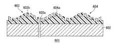
具体的には、基板の一面上に、使用する光波長に対して透明なポリマー(高分子樹脂)膜を形成し、その後このポリマー膜に対してフォトマスク露光及びウェットエッチングを行うことによって、上記と同様な光学素子を形成することも可能である。この方法によって形成した光学素子の構造例を図22に示す。図22に示す光学素子601では、ガラス等の基板602の一面側に、ポリマー膜を用いて形成された回折構造部603及びグリッド部604が配置されている。回折構造部603は凹部603a及び凸部603bを含み、これらの凹部603a及び凸部603bの表面に沿って、複数の微小凸部604aからなるグリッド部604が配置されている。
なお、図22に示した回折光学素子601においても、図21に示した実施形態と同様に基板の両面にグリッド部を設けることができる。Further, in the second embodiment, other manufacturing methods can be employed.
Specifically, a polymer (polymer resin) film that is transparent to the light wavelength to be used is formed on one surface of the substrate, and then the photomask exposure and wet etching are performed on the polymer film. It is also possible to form an optical element similar to the above. An example of the structure of an optical element formed by this method is shown in FIG. In the
In the diffractive
また、上記以外にも、型成形が可能であり、使用する光波長に対して透明な高屈折率ガラス(n=2.0程度)を用いて、回折構造部を有する基板を一体成形してもよい。この場合、屈折率が高いことにより、回折構造部の深さgをより小さくすることが可能となるので、グリッド部を形成する上で好ましい。
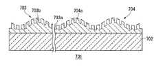
また、基板上に他の膜(例えば、SiO2などの無機膜)を形成し、この膜を選択的にエッチングすることにより回折構造部を形成することもできる。この方法によって形成された光学素子の構造例を図23に示す。図23に示す光学素子701では、ガラス等の基板702の一面側に、SiO2などの膜を用いて形成された回折構造部703が配置されている。回折構造部703は凹部703a及び凸部703bを含み、これらの凹部703a及び凸部703bの表面に沿って、複数の微小凸部704aからなるグリッド部704が配置されている。
なお、図23に示した回折光学素子701においても、図21に示した実施形態と同様に基板の両面にグリッド部を設けることができる。In addition to the above, mold forming is possible, and a substrate having a diffractive structure is integrally formed using high refractive index glass (n = 2.0) that is transparent to the light wavelength used. Also good. In this case, since the refractive index is high, the depth g of the diffractive structure portion can be further reduced, which is preferable in forming the grid portion.
Alternatively, the diffraction structure can be formed by forming another film (for example, an inorganic film such as SiO2) on the substrate and selectively etching the film. An example of the structure of an optical element formed by this method is shown in FIG. In an
Also in the diffractive
1,101,201,301,401,501,601,701:光学素子、2,102,202,302,402,502,602,702:基板、3,103,203,303,403,503,603,703:回折構造部、3a,103a,203a,303a,403a,503a,603a,703a:凹部、3b,103b,203b,303b,403b,503b,603b,703b:凸部、4,104,204,304,404,504,604,704:グリッド部、4a,104a,204a,304a,404a,504a,604a,704a:微小凸部、9,409:感光膜,10:液体、11:平行平板(基板)、12:水溶性膜1, 101, 201, 301, 401, 501, 601, 701: Optical element, 2, 102, 202, 302, 402, 502, 602, 702: Substrate, 3, 103, 203, 303, 403, 503, 603 703: diffractive structure, 3a, 103a, 203a, 303a, 403a, 503a, 603a, 703a: concave, 3b, 103b, 203b, 303b, 403b, 503b, 603b, 703b: convex, 4, 104, 204, 304, 404, 504, 604, 704: Grid portion, 4a, 104a, 204a, 304a, 404a, 504a, 604a, 704a: Minute convex portion, 9,409: Photosensitive film, 10: Liquid, 11: Parallel plate (substrate) ), 12: Water-soluble membrane
本発明に係る回折光学素子は、基板と、前記基板の一面側に設けられ、複数の凸部と複数の凹部とを有する回折構造部と、前記複数の凸部の上面、前記複数の凹部の上面、前記基板の他面、の少なくとも何れかが、前記複数の凸部の各々よりも小さい複数の微小凸部を含むグリッド部と、を有し、前記回折構造部は、各凸部及び凹部がマトリクス状に配列されている回折光学素子である。
また、回折光学素子は、(a)基板と、(b)複数の凸部又は複数の凹部を含み、上記基板の一面側に設けられた回折構造部と、(c)上記複数の凸部の各々よりも小さい複数の微小凸部を含み、上記回折構造部の上面又は上記基板の他面の少なくとも何れかに設けられたグリッド部と、を含み、上記回折構造部の断面形状が矩形であり、上記グリッド部が誘電体材料からなる、回折光学素子である。
The diffractive optical element according to the present invention includes asubstrate, a diffractive structure provided on one surface side of the substrate, having a plurality of convex portions and a plurality of concave portions, an upper surface of the plurality of convex portions, and a plurality of the concave portions. At least one of the upper surface and the other surface of the substrate includes a grid portion including a plurality of minute convex portions smaller than each of the plurality of convex portions, and the diffraction structure portion includes each convex portion and a concave portion. Are diffractive optical elements arranged in a matrix.
The diffractive optical element includes: (a) a substrate; (b) a plurality of convex portions or a plurality of concave portions, and a diffractive structure portion provided on one surface side of the substrate; and (c) the plurality of convex portions. A plurality of small convex portions smaller than each, and a grid portion provided on at least one of the upper surface of the diffractive structure portion or the other surface of the substrate, and the cross-sectional shape of the diffractive structure portion is rectangular The grid part is a diffractive optical element made of a dielectric material.
次に、本発明の回折光学素子の製造方法は、基板と、前記基板の一面側に設けられ、複数の凸部と複数の凹部とがマトリクス状に配列されてなる回折構造部と、前記複数の凸部の上面、前記複数の凹部の上面、前記基板の他面、の少なくとも何れかに誘電体材料を用いて形成され、前記複数の凸部の各々よりも小さい複数の微小凸部を含むグリッド部と、を有する回折光学素子の製造方法であって、前記基板上に前記複数の凸部を覆う感光膜を形成する工程と、屈折率が1より大きく前記感光膜の屈折率と同等かそれより低い値である液体が前記感光膜を覆うように配置する工程と、前記液体を挟んで、透明な平行平板を前記基板と対向配置する工程と、前記平行平板及び前記液体を介して前記感光膜を露光する工程と、前記液体及び前記平行平板を除去した後に前記感光膜を現像する工程と、前記感光膜のパターンをマスクとして前記基板をエッチングする工程と、を有する回折光学素子の製造方法である。
また、基板と、上記基板の一面側に設けられた複数の凸部を含む回折構造部と、上記回折構造部の上面又は上記基板の他面の少なくとも一方に誘電体材料を用いて形成され、上記複数の凸部の各々よりも小さい複数の微小凸部を含むグリッド部と、を有する回折光学素子の製造方法であって、上記基板上に複数の上記凸部を覆う感光膜を形成する工程と、屈折率が1より大きく上記感光膜の屈折率と同等かそれより低い値である液体を上記感光膜を覆うように配置する工程と、上記液体を挟んで、透明な平行平板を上記基板と対向配置する工程と、上記平行平板及び上記液体を介して上記感光膜を露光する工程と、上記液体及び上記平行平板を除去した後に上記感光膜を現像する工程と、上記感光膜のパターンをマスクとして上記基板をエッチングする工程と、を有する回折光学素子の製造方法である。
Next, the method for manufacturing a diffractive optical element according to the present invention includes asubstrate, a diffractive structure provided on one surface side of the substrate, in which a plurality of convex portions and a plurality of concave portions are arranged in a matrix, and the plurality And a plurality of minute protrusions that are smaller than each of the plurality of protrusions, and are formed using a dielectric material on at least one of the upper surface of the protrusions, the upper surface of the plurality of recesses, and the other surface of the substrate. And a step of forming a photosensitive film covering the plurality of convex portions on the substrate, and a refractive index greater than 1 and equal to the refractive index of the photosensitive film. A step of disposing a liquid having a lower value so as to cover the photosensitive film; a step of disposing a transparent parallel flat plate across the liquid; and the step of disposing the liquid through the parallel flat plate and the liquid. Exposing the photosensitive film, the liquid and the flat And a step of developing the photosensitive layer after removing the flat plate, and etching the substrate a pattern of the photoresist as a mask, a method for manufacturing a diffractive optical element having a.
In addition, the substrate, a diffractive structure including a plurality of protrusions provided on one surface of the substrate, and a dielectric material is formed on at least one of the upper surface of the diffractive structure and the other surface of the substrate, A method of manufacturing a diffractive optical element having a grid portion including a plurality of small convex portions smaller than each of the plurality of convex portions, and forming a photosensitive film covering the plurality of convex portions on the substrate A liquid having a refractive index larger than 1 and a value equal to or lower than the refractive index of the photosensitive film so as to cover the photosensitive film, and a transparent parallel plate sandwiched between the liquid and the substrate. A step of exposing the photosensitive film through the parallel plate and the liquid, a step of developing the photosensitive film after removing the liquid and the parallel plate, and a pattern of the photosensitive film. Use the above substrate as a mask. A step of bridging a method for manufacturing a diffractive optical element having a.
また本発明の回折光学素子の製造方法は、基板と、前記基板の一面側に設けられ、複数の凸部と複数の凹部とがマトリクス状に配列されてなる回折構造部と、前記複数の凸部の上面、前記複数の凹部の上面、前記基板の他面、の少なくとも何れかに誘電体材料を用いて形成され、前記複数の凸部の各々よりも小さい複数の微小凸部を含むグリッド部と、を有する回折光学素子の製造方法であって、前記基板上に前記複数の凸部を覆う感光膜を形成する工程と、屈折率が1より大きく前記感光膜の屈折率と同等かそれより低い値である水溶性膜が前記感光膜を覆うように配置する工程と、前記水溶性膜を介して前記感光膜を露光する工程と、前記感光膜を現像する工程と、前記感光膜のパターンをマスクとして前記基板をエッチングする工程と、を有する回折光学素子の製造方法である。
また、基板と、上記基板の一面側に設けられた複数の凸部を含む回折構造部と、上記回折構造部の上面又は上記基板の他面の少なくとも一方に誘電体材料を用いて形成され、上記複数の凸部の各々よりも小さい複数の微小凸部を含むグリッド部と、を有する回折光学素子の製造方法であって、上記基板上に複数の上記凸部を覆う感光膜を形成する工程と、屈折率が1より大きく上記感光膜の屈折率と同等かそれより低い値である水溶性膜を上記感光膜を覆うように配置する工程と、上記水溶性膜を介して上記感光膜を露光する工程と、上記感光膜を現像する工程と、上記感光膜のパターンをマスクとして上記基板をエッチングする工程と、を有する回折光学素子の製造方法である。The diffractive optical element manufacturing method of the present invention includes asubstrate, a diffractive structure provided on one side of the substrate, in which a plurality of convex portions and a plurality of concave portions are arranged in a matrix, and the plurality of convex portions. A grid portion including a plurality of minute convex portions smaller than each of the plurality of convex portions, formed using a dielectric material on at least one of an upper surface of the portion, an upper surface of the plurality of concave portions, and the other surface of the substrate. And a step of forming a photosensitive film covering the plurality of convex portions on the substrate, and a refractive index greater than 1 and equal to or higher than the refractive index of the photosensitive film. A step of disposing a water-soluble film having a low value so as to cover the photosensitive film, a step of exposing the photosensitive film through the water-soluble film, a step of developing the photosensitive film, and a pattern of the photosensitive film Etching the substrate using as a mask; and Amethod for producing a diffractive optical element having a.
In addition, the substrate, a diffractive structure including a plurality of protrusions provided on one surface of the substrate, and a dielectric material is formed on at least one of the upper surface of the diffractive structure and the other surface of the substrate, A method of manufacturing a diffractive optical element having a grid portion including a plurality of small convex portions smaller than each of the plurality of convex portions, and forming a photosensitive film covering the plurality of convex portions on the substrate A step of disposing a water-soluble film having a refractive index greater than 1 and a value equal to or lower than the refractive index of the photosensitive film so as to cover the photosensitive film, and the photosensitive film through the water-soluble film. A method for producing a diffractive optical element, comprising: an exposure step; a step of developing the photosensitive film; and a step of etching the substrate using a pattern of the photosensitive film as a mask.
Claims (13)
Translated fromJapanese前記基板の一面側に設けられた、複数の凸部を含む回折構造部と、
前記回折構造部の上面又は前記基板の他面の少なくとも何れかに設けられた、前記複数の凸部の各々よりも小さい複数の微小凸部を含むグリッド部と、
を含み、前記回折構造部の断面形状が矩形であり、前記グリッド部が誘電体材料からなる、
回折光学素子。A substrate,
A diffractive structure portion including a plurality of convex portions provided on one surface side of the substrate;
A grid portion provided on at least one of the upper surface of the diffractive structure portion or the other surface of the substrate and including a plurality of small convex portions smaller than each of the plurality of convex portions;
The cross-sectional shape of the diffractive structure portion is rectangular, and the grid portion is made of a dielectric material,
Diffractive optical element.
前記基板の一面側に設けられた周期的な曲面形状を有する複数の凸部を含む回折構造部と、
前記回折構造部の上面又は前記基板の他面の少なくとも一方に設けられ、前記複数の凸部の各々よりも小さい複数の微小凸部を含むグリッド部と、
を有する回折光学素子。A substrate,
A diffractive structure portion including a plurality of convex portions having a periodically curved shape provided on one surface side of the substrate;
A grid portion that is provided on at least one of the upper surface of the diffractive structure portion or the other surface of the substrate, and includes a plurality of small convex portions smaller than each of the plurality of convex portions;
A diffractive optical element.
請求項1又は2に記載の回折光学素子。Each of the plurality of minute convex portions of the grid portion extends in one direction.
The diffractive optical element according to claim 1 or 2.
請求項3に記載の回折光学素子。The extending direction of each of the plurality of convex portions of the diffractive structure portion and the extending direction of each of the plurality of minute convex portions of the grid portion are substantially parallel.
The diffractive optical element according to claim 3.
請求項3に記載の回折光学素子。The extending direction of each of the plurality of convex portions of the diffractive structure portion intersects with the extending direction of each of the plurality of minute convex portions of the grid portion,
The diffractive optical element according to claim 3.
請求項1又は2に記載の回折光学素子。Each of the plurality of minute convex portions of the grid portion is arranged in a planar distribution.
The diffractive optical element according to claim 1 or 2.
請求項1又は2に記載の回折光学素子。The depth of the grid part is shallower than the depth of the diffraction structure part,
The diffractive optical element according to claim 1 or 2.
請求項1乃至7のいずれか1項に記載の回折光学素子。The diffractive structure branches the incident light into a plurality of beams.
The diffractive optical element according to claim 1.
レーザー加工方法。Laser light is incident on the diffractive optical element according to claim 8 to branch the laser light into a plurality of beams, and irradiate the target with the plurality of beams.
Laser processing method.
前記基板上に複数の前記凸部を覆う感光膜を形成する工程と、
屈折率が1より大きく前記感光膜の屈折率と同等かそれより低い値である液体を前記感光膜を覆うように配置する工程と、
前記液体を挟んで、透明な平行平板を前記基板と対向配置する工程と、
前記平行平板及び前記液体を介して前記感光膜を露光する工程と、
前記液体及び前記平行平板を除去した後に前記感光膜を現像する工程と、
前記感光膜のパターンをマスクとして前記基板をエッチングする工程と、
を有する回折光学素子の製造方法。A plurality of convex portions provided on one side of the substrate, a plurality of convex portions, and at least one of the upper surface of the diffractive structure portion and the other surface of the substrate, and the plurality of A grid part including a plurality of micro convex parts smaller than each of the convex parts, and a method of manufacturing a diffractive optical element,
Forming a photosensitive film covering the plurality of convex portions on the substrate;
Disposing a liquid having a refractive index greater than 1 and a value equal to or lower than the refractive index of the photosensitive film so as to cover the photosensitive film;
Placing a transparent parallel plate opposite the substrate with the liquid sandwiched therebetween;
Exposing the photosensitive film through the parallel plate and the liquid;
Developing the photosensitive film after removing the liquid and the parallel plate;
Etching the substrate using the pattern of the photosensitive film as a mask;
The manufacturing method of the diffractive optical element which has these.
前記基板上に複数の前記凸部を覆う感光膜を形成する工程と、
屈折率が1より大きく前記感光膜の屈折率と同等かそれより低い値である水溶性膜を前記感光膜を覆うように配置する工程と、
前記水溶性膜を介して前記感光膜を露光する工程と、
前記感光膜を現像する工程と、
前記感光膜のパターンをマスクとして前記基板をエッチングする工程と、
を有する回折光学素子の製造方法。A plurality of convex portions provided on one side of the substrate, a plurality of convex portions, and at least one of the upper surface of the diffractive structure portion and the other surface of the substrate, and the plurality of A grid part including a plurality of micro convex parts smaller than each of the convex parts, and a method of manufacturing a diffractive optical element,
Forming a photosensitive film covering the plurality of convex portions on the substrate;
Disposing a water-soluble film having a refractive index greater than 1 and a value equal to or lower than the refractive index of the photosensitive film so as to cover the photosensitive film;
Exposing the photosensitive film through the water-soluble film;
Developing the photosensitive film;
Etching the substrate using the pattern of the photosensitive film as a mask;
The manufacturing method of the diffractive optical element which has these.
Priority Applications (1)
| Application Number | Priority Date | Filing Date | Title |
|---|---|---|---|
| JP2013130998AJP2013210680A (en) | 2007-11-06 | 2013-06-21 | Diffraction optical element, method of manufacturing the same, and laser machining method |
Applications Claiming Priority (3)
| Application Number | Priority Date | Filing Date | Title |
|---|---|---|---|
| JP2007289050 | 2007-11-06 | ||
| JP2007289050 | 2007-11-06 | ||
| JP2013130998AJP2013210680A (en) | 2007-11-06 | 2013-06-21 | Diffraction optical element, method of manufacturing the same, and laser machining method |
Related Parent Applications (1)
| Application Number | Title | Priority Date | Filing Date |
|---|---|---|---|
| JP2008281269ADivisionJP5487592B2 (en) | 2007-11-06 | 2008-10-31 | Laser processing method |
Publications (1)
| Publication Number | Publication Date |
|---|---|
| JP2013210680Atrue JP2013210680A (en) | 2013-10-10 |
Family
ID=40866153
Family Applications (2)
| Application Number | Title | Priority Date | Filing Date |
|---|---|---|---|
| JP2008281269AExpired - Fee RelatedJP5487592B2 (en) | 2007-11-06 | 2008-10-31 | Laser processing method |
| JP2013130998AWithdrawnJP2013210680A (en) | 2007-11-06 | 2013-06-21 | Diffraction optical element, method of manufacturing the same, and laser machining method |
Family Applications Before (1)
| Application Number | Title | Priority Date | Filing Date |
|---|---|---|---|
| JP2008281269AExpired - Fee RelatedJP5487592B2 (en) | 2007-11-06 | 2008-10-31 | Laser processing method |
Country Status (2)
| Country | Link |
|---|---|
| US (1) | US20100020400A1 (en) |
| JP (2) | JP5487592B2 (en) |
Cited By (2)
| Publication number | Priority date | Publication date | Assignee | Title |
|---|---|---|---|---|
| JP2018072386A (en)* | 2016-10-24 | 2018-05-10 | 大日本印刷株式会社 | Diffraction optical element, holding jig, and light irradiation device |
| JP2022506595A (en)* | 2018-11-07 | 2022-01-17 | アプライド マテリアルズ インコーポレイテッド | Depth-adjusted tilt grid using gray tone lithography and tilt etching |
Families Citing this family (22)
| Publication number | Priority date | Publication date | Assignee | Title |
|---|---|---|---|---|
| US8415611B2 (en) | 2009-11-19 | 2013-04-09 | Seiko Epson Corporation | Sensor chip, sensor cartridge, and analysis apparatus |
| TWI453398B (en)* | 2009-11-19 | 2014-09-21 | Seiko Epson Corp | Sensor chip, sensor cartridge, and analysis apparatus |
| JP5560891B2 (en) | 2010-05-13 | 2014-07-30 | セイコーエプソン株式会社 | Optical device and analyzer |
| US20130089662A1 (en)* | 2010-07-12 | 2013-04-11 | Dexerials Corporation | Method of producing master plate, method of producing alignment film, method of producing retardation film, and method of producing display device |
| JP5965194B2 (en)* | 2012-04-06 | 2016-08-03 | 株式会社フジクラ | Method for forming fine structure |
| KR101389320B1 (en)* | 2012-08-09 | 2014-04-29 | 한국표준과학연구원 | Apparatus and method for manufacturing phasetype diffraction element using laser exposure type |
| KR101576016B1 (en) | 2014-05-29 | 2015-12-10 | 한국기계연구원 | Laser Cutting Apparatus using Alternating Current and Cutting Method of the Same |
| JP6357892B2 (en)* | 2014-06-09 | 2018-07-18 | 凸版印刷株式会社 | Optical element |
| US10241244B2 (en) | 2016-07-29 | 2019-03-26 | Lumentum Operations Llc | Thin film total internal reflection diffraction grating for single polarization or dual polarization |
| US10473834B2 (en)* | 2016-11-21 | 2019-11-12 | Stmicroelectronics (Research & Development) Limited | Wafer level microstructures for an optical lens |
| FR3059110A1 (en) | 2016-11-21 | 2018-05-25 | Stmicroelectronics (Crolles 2) Sas | OPTICAL DIFFUSER AND METHOD FOR MANUFACTURING THE SAME |
| US20190067049A1 (en)* | 2017-08-23 | 2019-02-28 | Asm Technology Singapore Pte Ltd | Radiative wafer cutting using selective focusing depths |
| CN108802881B (en)* | 2018-05-21 | 2022-03-08 | 苏州大学 | A kind of high diffraction efficiency grating structure and preparation method |
| US11391957B2 (en) | 2018-10-29 | 2022-07-19 | Stmicroelectronics (Research & Development) Limited | Embedded transmissive diffractive optical elements |
| KR102070524B1 (en)* | 2018-12-31 | 2020-01-29 | 조정기 | Method and apparatus for manufacturing a film limiting viewing angle |
| CN111830605A (en)* | 2019-04-18 | 2020-10-27 | 上旸光学股份有限公司 | Optical Lenses with Laser-Induced Periodic Surface Microstructures |
| US12019252B2 (en) | 2019-11-26 | 2024-06-25 | Analog Devices, Inc. | Optical element with diffractive focusing features and diffractive anti-reflection features |
| CN111055009B (en)* | 2019-12-29 | 2020-11-17 | 中国科学院西安光学精密机械研究所 | Manufacturing method and system of inverted quadrangular frustum pyramid/quadrangular pyramid-shaped anti-reflection micro-nano structure |
| WO2021180549A1 (en) | 2020-03-11 | 2021-09-16 | Nil Technology Aps | Diffractive optical elements |
| US11662524B2 (en)* | 2020-03-13 | 2023-05-30 | Applied Materials, Inc. | Forming variable depth structures with laser ablation |
| JP7608902B2 (en)* | 2021-03-19 | 2025-01-07 | セイコーエプソン株式会社 | Lighting equipment and projectors |
| CN118707643B (en)* | 2024-08-28 | 2025-04-01 | 苏州弘德光电材料科技有限公司 | Optical film and optical device |
Citations (15)
| Publication number | Priority date | Publication date | Assignee | Title |
|---|---|---|---|---|
| JPH01246509A (en)* | 1988-03-28 | 1989-10-02 | Kuraray Co Ltd | A device consisting of an optical system including a polarizing element |
| JPH01252902A (en)* | 1988-04-01 | 1989-10-09 | Kuraray Co Ltd | Low reflection diffraction grating and its fabrication method |
| JPH06265710A (en)* | 1993-01-18 | 1994-09-22 | Canon Inc | Diffraction grating |
| JPH0895253A (en)* | 1994-09-21 | 1996-04-12 | Shin Etsu Chem Co Ltd | Water-soluble membrane material |
| JPH08240802A (en)* | 1995-03-03 | 1996-09-17 | Omron Corp | Optical element and its production |
| JPH09153446A (en)* | 1995-11-30 | 1997-06-10 | Sharp Corp | Interference exposure apparatus and interference exposure method using the same |
| JP2002062419A (en)* | 2000-06-07 | 2002-02-28 | Canon Inc | Diffractive optical element, optical apparatus having the diffractive optical element |
| JP2002341124A (en)* | 2001-05-18 | 2002-11-27 | Alps Electric Co Ltd | Diffraction grating member |
| JP2003025085A (en)* | 2001-07-12 | 2003-01-28 | Seiko Epson Corp | Laser processing method and laser processing apparatus |
| JP2003121619A (en)* | 2001-10-19 | 2003-04-23 | National Institute Of Advanced Industrial & Technology | Optical element and manufacturing method thereof |
| JP2003344630A (en)* | 2002-05-29 | 2003-12-03 | Alps Electric Co Ltd | Optical member |
| JP2004145064A (en)* | 2002-10-25 | 2004-05-20 | Dainippon Printing Co Ltd | Method for manufacturing diffractive optical element, diffractive optical element, optical system, and optical pickup device |
| JP2005259235A (en)* | 2004-03-11 | 2005-09-22 | Sanyo Electric Co Ltd | Optical pickup |
| JP2006185562A (en)* | 2004-12-28 | 2006-07-13 | Sanyo Electric Co Ltd | Optical element for optical pickup |
| WO2008156009A1 (en)* | 2007-06-19 | 2008-12-24 | Alps Electric Co., Ltd. | Optical element and method for manufacturing the same |
Family Cites Families (17)
| Publication number | Priority date | Publication date | Assignee | Title |
|---|---|---|---|---|
| JPS4920236B1 (en)* | 1970-07-28 | 1974-05-23 | ||
| JP2002263876A (en)* | 1993-06-04 | 2002-09-17 | Seiko Epson Corp | Laser processing apparatus and laser processing method |
| KR960703469A (en)* | 1994-05-02 | 1996-08-17 | 프레데릭 얀 스미트 | Optical transmissive component with anti-reflection gratings |
| JPH0829604A (en)* | 1994-07-11 | 1996-02-02 | Canon Inc | Method for producing diffraction grating pattern with limited area |
| JPH0936017A (en)* | 1995-07-20 | 1997-02-07 | Hitachi Ltd | Pattern forming method and semiconductor element manufacturing method using the same |
| JP3460580B2 (en)* | 1998-05-25 | 2003-10-27 | 日本ビクター株式会社 | Method of manufacturing hologram lens |
| JP3368225B2 (en)* | 1999-03-11 | 2003-01-20 | キヤノン株式会社 | Method for manufacturing diffractive optical element |
| JP3371846B2 (en)* | 1999-04-06 | 2003-01-27 | 日本電気株式会社 | Hologram element |
| US6590695B1 (en)* | 2002-02-26 | 2003-07-08 | Eastman Kodak Company | Micro-mechanical polarization-based modulator |
| JP4250906B2 (en)* | 2002-04-23 | 2009-04-08 | コニカミノルタホールディングス株式会社 | Optical element |
| EP1529230A4 (en)* | 2002-06-28 | 2010-06-16 | Technion Res & Dev Foundation | Geometrical phase optical elements with space-variant subwavelength gratings |
| TWI230834B (en)* | 2003-12-31 | 2005-04-11 | Ind Tech Res Inst | High-transmissivity polarizing module constituted with sub-wavelength structure |
| US7619816B2 (en)* | 2004-12-15 | 2009-11-17 | Api Nanofabrication And Research Corp. | Structures for polarization and beam control |
| JP2006178312A (en)* | 2004-12-24 | 2006-07-06 | Canon Inc | Surface reflection type phase grating |
| KR100707165B1 (en)* | 2005-06-11 | 2007-04-13 | 삼성전기주식회사 | Lighting device for flat display device and flat display device having same |
| JP5380796B2 (en)* | 2006-07-07 | 2014-01-08 | ソニー株式会社 | Polarizing element and liquid crystal projector |
| US7944544B2 (en)* | 2007-06-07 | 2011-05-17 | Seiko Epson Corporation | Liquid crystal device having a diffraction function layer that includes a flat portion and a non-flat portion with a grid disposed in the non-flat portion |
- 2008
- 2008-10-31JPJP2008281269Apatent/JP5487592B2/ennot_activeExpired - Fee Related
- 2008-11-06USUS12/265,761patent/US20100020400A1/ennot_activeAbandoned
- 2013
- 2013-06-21JPJP2013130998Apatent/JP2013210680A/ennot_activeWithdrawn
Patent Citations (15)
| Publication number | Priority date | Publication date | Assignee | Title |
|---|---|---|---|---|
| JPH01246509A (en)* | 1988-03-28 | 1989-10-02 | Kuraray Co Ltd | A device consisting of an optical system including a polarizing element |
| JPH01252902A (en)* | 1988-04-01 | 1989-10-09 | Kuraray Co Ltd | Low reflection diffraction grating and its fabrication method |
| JPH06265710A (en)* | 1993-01-18 | 1994-09-22 | Canon Inc | Diffraction grating |
| JPH0895253A (en)* | 1994-09-21 | 1996-04-12 | Shin Etsu Chem Co Ltd | Water-soluble membrane material |
| JPH08240802A (en)* | 1995-03-03 | 1996-09-17 | Omron Corp | Optical element and its production |
| JPH09153446A (en)* | 1995-11-30 | 1997-06-10 | Sharp Corp | Interference exposure apparatus and interference exposure method using the same |
| JP2002062419A (en)* | 2000-06-07 | 2002-02-28 | Canon Inc | Diffractive optical element, optical apparatus having the diffractive optical element |
| JP2002341124A (en)* | 2001-05-18 | 2002-11-27 | Alps Electric Co Ltd | Diffraction grating member |
| JP2003025085A (en)* | 2001-07-12 | 2003-01-28 | Seiko Epson Corp | Laser processing method and laser processing apparatus |
| JP2003121619A (en)* | 2001-10-19 | 2003-04-23 | National Institute Of Advanced Industrial & Technology | Optical element and manufacturing method thereof |
| JP2003344630A (en)* | 2002-05-29 | 2003-12-03 | Alps Electric Co Ltd | Optical member |
| JP2004145064A (en)* | 2002-10-25 | 2004-05-20 | Dainippon Printing Co Ltd | Method for manufacturing diffractive optical element, diffractive optical element, optical system, and optical pickup device |
| JP2005259235A (en)* | 2004-03-11 | 2005-09-22 | Sanyo Electric Co Ltd | Optical pickup |
| JP2006185562A (en)* | 2004-12-28 | 2006-07-13 | Sanyo Electric Co Ltd | Optical element for optical pickup |
| WO2008156009A1 (en)* | 2007-06-19 | 2008-12-24 | Alps Electric Co., Ltd. | Optical element and method for manufacturing the same |
Cited By (3)
| Publication number | Priority date | Publication date | Assignee | Title |
|---|---|---|---|---|
| JP2018072386A (en)* | 2016-10-24 | 2018-05-10 | 大日本印刷株式会社 | Diffraction optical element, holding jig, and light irradiation device |
| JP2022506595A (en)* | 2018-11-07 | 2022-01-17 | アプライド マテリアルズ インコーポレイテッド | Depth-adjusted tilt grid using gray tone lithography and tilt etching |
| JP7277581B2 (en) | 2018-11-07 | 2023-05-19 | アプライド マテリアルズ インコーポレイテッド | Depth-tuned tilted grating using graytone lithography and tilted etching |
Also Published As
| Publication number | Publication date |
|---|---|
| JP2009134287A (en) | 2009-06-18 |
| JP5487592B2 (en) | 2014-05-07 |
| US20100020400A1 (en) | 2010-01-28 |
Similar Documents
| Publication | Publication Date | Title |
|---|---|---|
| JP5487592B2 (en) | Laser processing method | |
| US11855348B2 (en) | Metasurface-assisted 3D beam shaping using array of scatterers | |
| TWI764107B (en) | Diffraction light guide plate and eyewear | |
| KR100693024B1 (en) | Manufacturing method of microstructure, exposure apparatus, electronic device | |
| US12287571B1 (en) | Method and apparatus for fabrication of large area 3D photonic crystals with embedded waveguides | |
| CN111175881B (en) | Waveguide device, method for manufacturing grating portion in waveguide device, and display device | |
| JP6882316B2 (en) | Wire grid polarizing plate manufacturing method | |
| WO2019029349A1 (en) | Backlight assembly and preparation method therefor, and display device | |
| JP2007057622A (en) | Optical element and manufacturing method thereof, manufacturing method of shape transfer mold for optical element, and transfer mold for optical element | |
| WO2010131440A1 (en) | Sheet and light-emitting device | |
| JP5391670B2 (en) | Manufacturing method of fine structure | |
| JP2022536694A (en) | Optical eyepiece using single-sided patterning of grating couplers | |
| Lalanne et al. | Artificial media optical properties-subwavelength scale | |
| US10509327B1 (en) | Variable neutral density filter for multi-beam interference lithography exposure | |
| JP2009103786A (en) | Diffraction grating fabrication method using phase mask for diffraction grating fabrication | |
| KR100471380B1 (en) | Method for Manufacturing Optical Waveguide Using Laser Direct Writing And Optical Waveguide Using the Same | |
| JP6221849B2 (en) | Exposure method, method for manufacturing fine periodic structure, method for manufacturing grid polarizing element, and exposure apparatus | |
| US20150198812A1 (en) | Photo-Mask and Accessory Optical Components for Fabrication of Three-Dimensional Structures | |
| CN103777263B (en) | The method for making of sub-wavelength rectangle monocycle optical grating construction and even number beam splitter | |
| WO2017051443A1 (en) | Exposure method, method for manufacturing microperiodical structure, method for manufacturing grid polarizer elements, and exposure equipment | |
| JP2016206677A (en) | Method for manufacturing holographic optical element and display device including holographic optical element by this method | |
| KR20220148321A (en) | A method for producing a continuously diffractive optical element, an apparatus for performing the production method, and a continuously diffractive optical element | |
| KR102767847B1 (en) | Grating device and method of manufacturing the same and optical apparatus including grating device | |
| US10914944B1 (en) | Anti-refraction cancelling prism for multi-beam interference lithography exposure | |
| JP5757413B2 (en) | Phase modulation mask, exposure apparatus and exposure method |
Legal Events
| Date | Code | Title | Description |
|---|---|---|---|
| A521 | Request for written amendment filed | Free format text:JAPANESE INTERMEDIATE CODE: A523 Effective date:20130719 | |
| A621 | Written request for application examination | Free format text:JAPANESE INTERMEDIATE CODE: A621 Effective date:20130719 | |
| A977 | Report on retrieval | Free format text:JAPANESE INTERMEDIATE CODE: A971007 Effective date:20140515 | |
| A131 | Notification of reasons for refusal | Free format text:JAPANESE INTERMEDIATE CODE: A131 Effective date:20140603 | |
| A521 | Request for written amendment filed | Free format text:JAPANESE INTERMEDIATE CODE: A523 Effective date:20140731 | |
| A131 | Notification of reasons for refusal | Free format text:JAPANESE INTERMEDIATE CODE: A131 Effective date:20141219 | |
| A761 | Written withdrawal of application | Free format text:JAPANESE INTERMEDIATE CODE: A761 Effective date:20150206 |