JP2013201380A - Reflecting material and lighting device - Google Patents
Reflecting material and lighting deviceDownload PDFInfo
- Publication number
- JP2013201380A JP2013201380AJP2012070043AJP2012070043AJP2013201380AJP 2013201380 AJP2013201380 AJP 2013201380AJP 2012070043 AJP2012070043 AJP 2012070043AJP 2012070043 AJP2012070043 AJP 2012070043AJP 2013201380 AJP2013201380 AJP 2013201380A
- Authority
- JP
- Japan
- Prior art keywords
- light emitting
- layer
- reflective
- emitting module
- average particle
- Prior art date
- Legal status (The legal status is an assumption and is not a legal conclusion. Google has not performed a legal analysis and makes no representation as to the accuracy of the status listed.)
- Pending
Links
Images

Landscapes
- Led Device Packages (AREA)
- Non-Portable Lighting Devices Or Systems Thereof (AREA)
Abstract
Translated fromJapaneseDescription
Translated fromJapanese本発明の実施形態は、反射材及び照明装置に関する。 Embodiments described herein relate generally to a reflector and a lighting device.
近年、照明分野において、発光素子の発光効率の高効率化が進んでいる。発光効率の高効率化に伴い、高反射率を有する構成材料が要求されている。例えば、発光素子が搭載された発光モジュールでは、有機系バインダーにAl2O3などの無機系酸化物が添加された反射コート材が用いられている。なお、発光素子が搭載される金属基板として、金属基板上に絶縁樹脂層が設けられ、絶縁樹脂層上にセラミック層が設けられた基板がある。In recent years, in the lighting field, the efficiency of light emitting elements has been increasing. With increasing luminous efficiency, constituent materials having high reflectivity are required. For example, in a light emitting module on which a light emitting element is mounted, a reflective coating material in which an inorganic oxide such as Al2 O3 is added to an organic binder is used. Note that as a metal substrate on which a light-emitting element is mounted, there is a substrate in which an insulating resin layer is provided over a metal substrate and a ceramic layer is provided over the insulating resin layer.
本発明が解決しようとする課題は、反射率の高い反射剤及び照明装置を提供することである。 The problem to be solved by the present invention is to provide a reflective agent and a lighting device having high reflectivity.
実施形態に係る反射剤は、バインダーを有する。実施形態に係る反射剤は、前記バインダーに添加された平均粒径の異なる2種類のフィラーであって、該フィラーの2種類の平均粒径を平均粒径が大きい順にD1、D2とした場合に、数式:0.1≦(D2/D1)≦0.4を満足するフィラーを具備する。実施形態に係る反射剤は、発光モジュールの反射層に用いられる。 The reflective agent according to the embodiment has a binder. The reflective agent which concerns on embodiment is two types of fillers from which the average particle diameter added to the said binder differs, Comprising: When the two types of average particle diameter of this filler are set to D1 and D2 in order with a large average particle diameter, And a filler satisfying 0.1 ≦ (D2 / D1) ≦ 0.4. The reflective agent which concerns on embodiment is used for the reflection layer of a light emitting module.
(実施形態)
開示の反射剤は、発光素子における反射層に用いられる。反射剤は、バインダーと、バインダーに添加された平均粒径の異なる2種類のフィラーとを有する。発光素子は、任意の発光素子であって良く、例えば、LED(Light Emitting Diode)素子や有機EL(Electro Luminescence)素子などである。発光素子は、例えば、スポットライトやダウンライト、防犯灯、ブラケットライト、ペンダントライトなど、任意の照明装置に用いられる。(Embodiment)
The disclosed reflective agent is used for a reflective layer in a light-emitting element. A reflective agent has a binder and two types of fillers with different average particle diameters added to the binder. The light emitting element may be an arbitrary light emitting element, such as an LED (Light Emitting Diode) element or an organic EL (Electro Luminescence) element. A light emitting element is used for arbitrary illuminating devices, such as a spotlight, a downlight, a security light, a bracket light, a pendant light, for example.
バインダーは、無機バインダー又は有機バインダーであり、任意のバインダーであって良い。無機バインダーは、例えば、SiO2である。有機バインダーは、例えば、ポリイミドである。フィラーは、無機系酸化物であり、好ましくは、白色系の無機酸化物フィラーである。白色系の無機酸化物フィラーとは、例えば、Al2O3である。The binder is an inorganic binder or an organic binder, and may be any binder. Inorganic binder is, for example, SiO2. The organic binder is, for example, polyimide. The filler is an inorganic oxide, preferably a white inorganic oxide filler. The white inorganic oxide filler is, for example, Al2 O3 .
ここで、フィラーの2種類の平均粒径を平均粒径が大きい順にD1、D2とした場合に、数式:0.1≦(D2/D1)≦0.4を満足することが好ましい。(D2/D1)が1である場合には、フィラーの平均粒径に差がないことを示す。平均粒径に差を設けるという観点から、0.4以下であることが好ましい。また、2種類の平均粒径に差がありすぎると、相対的に平均粒径が小さいフィラーが、相対的に平均粒径が大きいフィラーの隙間を効率的に埋めることができないと考えられる。このことから、(D2/D1)が0.1以上であることが好ましい。また、0.15≦(D2/D1)≦0.4を満足することがより好ましく、更に好ましくは、0.2≦(D2/D1)≦0.3を満足する場合である。 Here, when the two types of average particle diameters of the filler are D1 and D2 in descending order of the average particle diameter, it is preferable to satisfy the formula: 0.1 ≦ (D2 / D1) ≦ 0.4. When (D2 / D1) is 1, it indicates that there is no difference in the average particle diameter of the filler. From the viewpoint of providing a difference in average particle diameter, it is preferably 0.4 or less. Moreover, when there is too much difference between the two types of average particle diameters, it is considered that a filler having a relatively small average particle diameter cannot efficiently fill a gap between fillers having a relatively large average particle diameter. Therefore, it is preferable that (D2 / D1) is 0.1 or more. Further, it is more preferable to satisfy 0.15 ≦ (D2 / D1) ≦ 0.4, and it is more preferable that 0.2 ≦ (D2 / D1) ≦ 0.3 is satisfied.
また、例えば、フィラーの平均粒径D1は、100μm以下であるとともに、平均粒径D1が3μm以上となる。また、フィラーのバインダーに対する添加量は、任意であって良い。また、例えば、フィラーのバインダーに対する添加量は、80vol%〜98vol%であることが好ましい。フィラーのバインダーに対する添加量を98vol%とすることで、下地との密着性を向上可能であり、剥離が生じる可能性を減少させることが可能となる。また、反射剤自体にクラックが発生する可能性を低減可能である。また、フィラーのバインダーに対する添加量を80vol%以上とすることで、透過率を抑制出来、これにより、下地の影響が低減可能となる。また、2種類の平均粒径が異なるフィラーの混合比は、任意であって良い。2種類の平均粒径が異なるフィラーの混合比は、好ましくは、D1:D2=5:1〜2:1(vol%)であり、より好ましくは、D1:D2=4:1(vol%)である。この範囲外であると、隙間が埋まりにくいためである。 For example, the average particle diameter D1 of the filler is 100 μm or less, and the average particle diameter D1 is 3 μm or more. Moreover, the addition amount with respect to the binder of a filler may be arbitrary. For example, it is preferable that the addition amount with respect to the binder of a filler is 80 vol%-98 vol%. By setting the added amount of the filler to the binder to 98 vol%, it is possible to improve the adhesion with the base and reduce the possibility of peeling. Further, it is possible to reduce the possibility of cracks occurring in the reflective agent itself. Moreover, the transmittance | permeability can be suppressed because the addition amount with respect to the binder of a filler shall be 80 vol% or more, Thereby, the influence of a foundation | substrate can be reduced. Moreover, the mixing ratio of the two types of fillers having different average particle diameters may be arbitrary. The mixing ratio of the two types of fillers having different average particle diameters is preferably D1: D2 = 5: 1 to 2: 1 (vol%), more preferably D1: D2 = 4: 1 (vol%). It is. This is because if it is outside this range, the gap is difficult to fill.
また、開示の反射剤が用いられる発光モジュールは、基板と、基板上に設けられた白色レジスト層と、反射層とを有する。また、開示の反射剤が用いられる反射層は、白色レジスト層上に設けられる。以下では、図1〜図3を用いて、開示の反射剤が用いられる発光素子の構造の一例を示す。以下では、セラミック基板を用いた実施形態の一例における発光モジュールの断面図の一例、金属基板を用いた実施形態の一例における発光モジュールの断面図の一例、発光モジュールの平面図の一例について順に説明する。 In addition, a light emitting module in which the disclosed reflective agent is used includes a substrate, a white resist layer provided on the substrate, and a reflective layer. Moreover, the reflective layer in which the disclosed reflective agent is used is provided on the white resist layer. Hereinafter, an example of the structure of a light-emitting element in which the disclosed reflective agent is used will be described with reference to FIGS. Hereinafter, an example of a sectional view of a light emitting module in an example of an embodiment using a ceramic substrate, an example of a sectional view of a light emitting module in an example of an embodiment using a metal substrate, and an example of a plan view of the light emitting module will be described in order. .
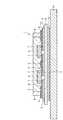
図1は、セラミック基板を用いた実施形態の一例における発光モジュールの断面図の一例を示す図である。図1に示す例では、開示の反射剤が用いられた発光モジュール1は、セラミック基板2と、配線パターン3と、白色レジスト層4と、反射層5と、発光素子6と、ダイボンド材7と、反射枠8と、封止樹脂層9と、半田層10と、金属ヒートスプレッダ11とを有する。 FIG. 1 is a diagram illustrating an example of a cross-sectional view of a light emitting module in an example of an embodiment using a ceramic substrate. In the example shown in FIG. 1, the
配線パターン3は、セラミック基板2の上面と下面とに所定のパターンで設けられる。配線パターン3は、例えば、セラミック基板2の上面及び下面の全面に貼り合わせることで接合された銅層から、エッチングにより不要な部位を除去することで形成される。配線パターン3は、例えば、銅と、ニッケルと、金の三層構造をなしており、銅層は配線パターン3のベース層を形成し、ニッケル層が配線パターン3の中間層を形成し、金層が配線パターン3の表層を形成する。なお、図1に示す例では、配線パターン3がセラミック基板2の上面と下面との両方に形成される場合を例に示したが、これに限定されるものではなく、セラミック基板2の上面だけに合っても良い。なお、配線パターン3は、三層構造をなしていなくても良く、二層以下の構造でも良く、四層以上の構造でも良い。 The
白色レジスト層4は、セラミック基板2の上面に設けられる。白色レジスト層4は、例えば、フィラーを含まない白色の合成樹脂で形成される。白色レジスト層4は、例えばエポキシ樹脂からなる樹脂材で形成される。ただし、白色レジスト層4は、これに限定されるものではなく、白色レジスト層4がフィラーを含んでも良い。白色レジスト層は、例えば、スクリーン印刷によりセラミック基板2上に塗布される。白色レジスト層4は、発光素子6からセラミック基板2側に出射された高エネルギーの光を光の利用方向に反射する。 The
ここで、セラミック基板2の上面に設けられる配線パターン3と白色レジスト層4との関係について示す。配線パターン3は、セラミック基板2上に直接設けても良く、白色レジスト層4上に設けられても良い。また、配線パターン3は、セラミック基板2上に直接設けられる場合には、配線パターン3の上面に白色レジスト層4が設けられる。この場合、例えば、白色レジスト層4は、配線パターン3が設けられた箇所のうち、後述のダイボンド材7を介して発光素子6と配線パターン3とが接合される箇所を除いた箇所の上部に対して設けられる。 Here, the relationship between the
反射層5は、開示の反射剤を用いて形成される。反射層5は、白色レジスト層4上に設けられる。反射層5は、発光素子6からセラミック基板2側に出射された高エネルギーの光を光の利用方向に反射する。反射層5は、例えば、スクリーン印刷により白色レジスト層4上に塗布される。 The
反射層5と白色レジスト層4との関係について補足する。反射層5には、フィラーを含む反射剤が用いられており、白色レジスト層4と比較して反射率が高い。図1に示す例では、基板はセラミック基板2であり、セラミック基板2の上部に直接配線パターン3を設けることができ、セラミック基板2上に白色レジスト層4をあえて設けなくても良い。図1に示す例では、反射層5に加えて白色レジスト層4を更に設けることで、反射層5の厚さを薄くしても十分な反射率を得ることが可能となり、簡単かつ安価に実現可能となる。 The relationship between the
発光素子6は、光を発光する。例えば、発光素子6が青色LEDチップで形成される場合には、サファイア製の透光性素子基板の一面に半導体発光層と一対の素子電極を設けて形成される。半導体発光層は、例えば、455nm〜465nmのピーク波長を有した青色の光を放射する。青色の光は、半導体発光層から光の利用方向である表側に出射されるだけではなく、素子基板を透過して発光素子6の裏側にも出射される。なお、裏側に出射される光のエネルギー強度の方が、表側に出射される光のエネルギー強度より強い。なお、発光素子6は、青色LEDチップで形成される場合に限定されるものではなく、任意の色のLEDチップで形成されても良く、有機EL素子で形成されても良く、任意の発光素子で形成されて良い。 The
発光素子6は、ダイボンド材7を用いて、配線パターン3と接合される。図1に示す例では、列が延びる方向に隣接した発光素子6各々は、配線パターン3を介して、他の発光素子6の異極電極同士が接続される。なお、ダイボンド材7は、例えば、透明なシリコーン樹脂である。 The
反射枠8は、例えば、白色のシリコーン樹脂で形成される。図1に示す例では、反射枠8が反射層5上に設けられる場合を例に示したが、これに限定されるものではなく、セラミック基板2上に設けられても良い。反射枠8は、例えば、未硬化の状態で発光素子6が設けられる領域を囲んで塗布され、硬化処理されることで接着される。 The
封止樹脂層9は、反射枠8により囲まれる領域に充填される。封止樹脂層9は、透光性材料が用いられる。封止樹脂層9は、例えば、透明シリコーン樹脂により形成される。封止樹脂層9は、例えば、白色の照明光を得ることを目的として黄色の蛍光体が用いられている。 The sealing
半田層10は、セラミック基板2の下面に設けられ、後述の金属ヒートスプレッダ11をセラミック基板2と接合する。金属ヒートスプレッダ11は、セラミック基板2の熱を放出する。すなわち、金属ヒートスプレッダ11は、発光素子6の温度が上がり過ぎることを抑制する結果、発光素子6の発光性能と発光色を維持することが可能となる。 The
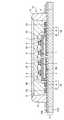
図2は、金属基板を用いた実施形態の一例における発光モジュールの断面図の一例を示す図である。図2では、図1を用いて説明したセラミック基板2を用いた場合における発光モジュールの断面図と同一の箇所については、同一の符号を用いて説明する。また、以下では、セラミック基板2を用いた場合における発光モジュールと同様の点については、適宜説明を省略する。 FIG. 2 is a diagram illustrating an example of a cross-sectional view of a light emitting module in an example of an embodiment using a metal substrate. In FIG. 2, the same portions as those in the cross-sectional view of the light emitting module when the
図2に示す例では、図1に示したセラミック基板2を用いた場合と比較して、発光モジュール1aが、セラミック基板2の代わりに、金属基板21を有する。金属基板21は、例えば、熱伝導性に優れた金属を用いて形成される。詳細な一例をあげて説明すると、金属基板21は、アルミニウム、又は、アルミニウムを含むアルミニウム合金を用いて形成される金属ベース21aと、金属ベース21a上に積層された絶縁層21bを有する。絶縁層21bは、例えば、合成樹脂で形成される。絶縁層21bの厚みは、金属ベース21aの厚みと比較して薄くて良い。 In the example illustrated in FIG. 2, the
また、図2に示す例では、発光モジュール1aが、配線パターン3の代わりに、互いに平行な給電パターンを有する配線パターン22を有する場合を例に示した。なお、図2に示す例では、配線パターン22は、三層構造を有する場合を例に示した。詳細な一例をあげて説明すると、配線パターン22は、ベース層Aと、中間層Bと、表層Cとを有する場合を例に示した。配線パターン22は、配線パターン3と同一の材料を用いて、配線パターン3と同様の手法にて形成される。 Further, in the example illustrated in FIG. 2, the case where the
また、図2に示す例では、発光モジュール1aが、発光素子6の実装位置を決める目安として用いられるアライメントマーク23を更に有する場合を例に示した。図2に示す例では、アライメントマーク23は、配線パターン22を間にはさんで両側に設けられる。アライメントマーク23は、例えば、配線パターン3と同一の材料を用いて、配線パターン3と同様の手法にて形成される。 In the example illustrated in FIG. 2, the
また、図2に示す例では、発光モジュール1aが、金属反射部位24と、金属反射部位24を覆うように設けられた白色レジスト層4と、白色レジスト層4を覆うように設けられた反射層5とを有する。 In the example shown in FIG. 2, the
図2に示す例では、金属反射部位24は、略四角形状であるが、これに限定されるものではなく、任意の形状であって良い。図2に示す例では、金属反射部位24は、絶縁層21bに接合固着される。金属反射部位24は、例えば、銅を用いて形成される。金属反射部位24は、例えば、配線パターン3のベース層Aと同一の材料を用いて、配線パターン3と同様の手法を用いて形成される。 In the example shown in FIG. 2, the
図2に示す例では、発光素子6が、ダイボンド材7を用いて反射層5上に接着され、反射層5上に接着された発光素子6各々がボンディングワイヤ25で直列に接続される場合を例に示した。言い換えると、ボンディングワイヤ25は、列が延びる方向に隣接した発光素子6の異極の素子電極同士を接続するように設けられる場合を例に示した。また、図2に示す例では、発光素子6の列の一端に配置された発光素子6と、隣接された配線パターン22とが、端部ボンディングワイヤ26で接続される場合を例に示した。なお、ボンディングワイヤ25及び端部ボンディングワイヤ26は、例えば、金属細線で形成される。より詳細な一例をあげて説明すると、ボンディングワイヤ25及び端部ボンディングワイヤ26は、例えば、金の細線を用いて形成される。 In the example shown in FIG. 2, the
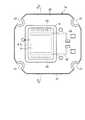
図3は、発光モジュールの平面図の一例を示す平面図である。図3に示す例では、説明の便宜上、図2に示した金属基板を用いた実施形態の一例における発光モジュールの平面図を示した。図3に示す例では、金属基板21の四隅に、発光モジュール1aを固定するためのねじ通し部27が設けられる場合を例に示したが、これに限定されるものではなく、ねじ通し部27を有さなくても良い。なお、ねじ通し部27は、例えば、金属基板21の四隅に溝を設けることで形成される。 FIG. 3 is a plan view illustrating an example of a plan view of the light emitting module. In the example shown in FIG. 3, the top view of the light emitting module in an example of embodiment using the metal substrate shown in FIG. 2 was shown for convenience of explanation. In the example shown in FIG. 3, the case where the screwing
なお、図2に示す例では、発光モジュール1aが金属反射部位24を有する場合を例に示したが、これに限定されるものではなく、金属反射部位24を有さなくても良い。また、例えば、上述した実施形態では、白色レジスト層4にフィラーが含まれない場合を例に示したが、これに限定されるものではなく、白色レジスト層4にフィラーが含まれても良い。この場合、白色レジスト層4に含まれるフィラーの割合を反射層5と比較し低くなるようにしても良い。 In the example shown in FIG. 2, the case where the
また、図1に示す例では、反射層5が白色レジスト層4上に設けられる場合を用いて説明したが、これに限定されるものではなく、白色レジスト層4を設けなくても良い。また、図1に示す例では、発光モジュール1がアライメントマーク23を有さない場合を例に示したが、これに限定されるものではなく、アライメントマーク23を更に有しても良い。また、図1に示す例では、発光素子6各々が配線パターン3により接続される場合を例に示したが、これに限定されるものではなく、図2に示すようにボンディングワイヤで接続されても良い。 In the example shown in FIG. 1, the case where the
上述したように、実施形態に係る反射剤は、バインダーと、酸化物にて形成された平均粒径の異なる2種類のフィラーであって、前記バインダーに添加されたフィラーとを具備する。この結果、反射率の高い反射剤及び照明装置を提供することが可能となる。具体的には、フィラーの充填率が高くなる結果、反射率の高い反射剤及び照明装置を提供可能となる。 As described above, the reflective agent according to the embodiment includes a binder and two types of fillers formed of an oxide and having different average particle diameters, and added to the binder. As a result, it is possible to provide a reflective agent and a lighting device with high reflectivity. Specifically, as a result of the high filler filling rate, it is possible to provide a reflective agent and a lighting device with high reflectivity.
また、2種類の異なる平均粒径を有するフィラーを用いることで、平均粒径を考慮しない場合と比較して、フィラーの充填率が高く透過率の低い反射材を実現可能となる。また、透過率の低い、言い換えると、反射率の高い反射剤を実現可能となる結果、高効率の発光モジュールや照明装置が実現可能となる。 In addition, by using two types of fillers having different average particle diameters, it is possible to realize a reflector having a high filler filling rate and a low transmittance as compared with the case where the average particle diameter is not taken into consideration. In addition, a reflective agent having a low transmittance, in other words, a high reflectance can be realized. As a result, a highly efficient light-emitting module and lighting device can be realized.
また、平均粒径を考慮しない場合と比較してフィラーの量を相対的に少なくしても高い反射率が得られる結果、フィラーの量を少なくすることが可能である。この結果、平均粒径を考慮しない場合と比較して、接着機能を果たす有機系バインダーの占める割合を増加でき、下地との密着性を向上可能であり、剥離が生じる可能性を減少させることが可能となる。また、反射剤自体にクラックが発生する可能性を低減可能である。 In addition, as compared with the case where the average particle size is not taken into account, even if the amount of the filler is relatively reduced, a high reflectance can be obtained. As a result, the amount of the filler can be reduced. As a result, compared to the case where the average particle size is not taken into account, the proportion of the organic binder that performs the adhesion function can be increased, the adhesion with the base can be improved, and the possibility of peeling is reduced. It becomes possible. Further, it is possible to reduce the possibility of cracks occurring in the reflective agent itself.
また、上述したように、フィラーの2種類の平均粒径を平均粒径が大きい順にD1、D2とした場合に、数式:0.1≦(D2/D1)≦0.4を満足する。他の範囲と比較して透過率を低くすることができ、反射率の高い反射剤及び照明装置を提供可能となる。 Further, as described above, when the two types of average particle diameters of the fillers are D1 and D2 in descending order of the average particle diameter, the mathematical formula: 0.1 ≦ (D2 / D1) ≦ 0.4 is satisfied. The transmittance can be lowered as compared with other ranges, and it is possible to provide a reflective agent and a lighting device having a high reflectance.
また、上述したように、D1が100μm以下であるとともに、D1が3μm以上となる。また、発光モジュールは、基板と、基板上に設けられた白色レジスト層と、反射層とを有し、反射層は、白色レジスト層上に設けられる。この結果、反射層を相対的に薄くすることが可能となる。また、反射層を相対的に薄くすることができる結果、反射層を厚くする場合と比較して熱膨張率差をあまり考慮しなくて良いという有利な効果を奏し、バインダーに対するフィラーの添加量に対する制限が減少するという有利な効果を奏する。 As described above, D1 is 100 μm or less, and D1 is 3 μm or more. The light emitting module includes a substrate, a white resist layer provided on the substrate, and a reflective layer, and the reflective layer is provided on the white resist layer. As a result, the reflective layer can be made relatively thin. In addition, as a result of the relatively thin reflective layer, there is an advantageous effect that it is not necessary to consider the difference in coefficient of thermal expansion as compared with the case where the reflective layer is thick. There is an advantageous effect that the restriction is reduced.
上述した発光モジュールによれば、フィラーが混入された反射剤を用いて形成された反射層5上に複数の発光素子6を実装することで、各発光素子6がその裏側に出射する高エネルギーの光を光の利用方向に反射させることが可能となる。反射層5の反射面は、銀の層からなる反射面と比較して低波長域の光成分を反射することができる分、銀メッキ層の反射面と比較して優れた光反射性能を実現可能となる。また、上述の反射剤を用いて反射層5が形成されることで、前記高エネルギーの光に晒されても劣化を防止することが可能となる。 According to the above-described light emitting module, by mounting a plurality of
ここで、この高エネルギーの光の一部は、反射層5を透過すると考えられる。反射層5を透過した透過光は、白色レジスト層4に入射して白色レジスト層4で光の利用方向に反射される。この結果、一次、二次の光反射が起こることで、発光素子6の裏側に出射された光の反射性能を向上可能となる。言い換えると、光の取出し性能が向上されることで、発光モジュール1の発光効率を向上可能となる。 Here, it is considered that a part of the high energy light is transmitted through the
また、上述したように、反射層5の下部に白色レジスト層4を設けることで、反射層5をできる限り薄くしたとしても、十分な反射性能を実現可能となる。また、反射層5のみを設けて白色レジスト層4を設けない場合と比較して、フィラーの使用量を少なくすることが可能となる。また、反射層5の厚さを薄くすることができる結果、反射層5の熱膨張率と発光モジュールの他の材料との間における熱膨張率に差が生じることを防止することも可能となる。 In addition, as described above, by providing the white resist
図4は、発光モジュールを装着した照明装置の一例を示す縦断面図である。図4に示す例では、照明装置100は、発光モジュール1を備える。また、照明装置100は、本体31、口金部材32a、アイレット部32b、カバー33、制御部34、電気配線34a、電極接合部34a−1、電気配線34b、電極接合部34b−1を備える。 FIG. 4 is a longitudinal sectional view showing an example of a lighting device equipped with a light emitting module. In the example illustrated in FIG. 4, the
発光モジュール1は、本体31の鉛直方向の上面に配置される。発光モジュール1は、セラミック基板2を備える。セラミック基板2は、低熱伝導率の陶磁素材、例えば、セラミックスにより形成される。セラミック基板2の熱伝導率は、例えば、300[K]大気雰囲気下において、約99.5質量%のアルミニウムの熱伝導率である225[W/m・K]よりも小さい。 The
セラミック基板2は、機械的強度、寸法精度も高いため、発光モジュール1を量産する際の歩留まり向上、発光モジュール1の製造コストの低減、発光モジュール1の長寿命化に寄与する。また、セラミックスは、可視光の反射率が高いため、LEDモジュールの発光効率を向上させる。 Since the
図4に示す例では、発光モジュール1が、発光素子6として、セラミック基板2の鉛直方向の上面の円周上に配置された青色LED41と、セラミック基板2の鉛直方向の上面の中心付近に配置された赤色LED42とを有する場合を示した。赤色LED42は、青色LED41と比較して、発光素子の温度の上昇とともに発光素子の発光量がさらに低下する。すなわち、赤色LED42は、青色LED41と比較して、発光素子の温度の上昇とともに発光素子の発光量がより低下するという点で熱特性が劣る。第1の実施形態は、セラミック基板2が、低熱伝導率の陶磁素材であるので、青色LED41が発した熱がセラミック基板2を介して赤色LED42へ伝導することを抑制し、赤色LED42の発光効率の悪化を抑制する。 In the example shown in FIG. 4, the
なお、図4では、青色LED41及び赤色LED42は、数を省略して記載している。すなわち、第1のLED群として、複数の青色LED41が、セラミック基板2の鉛直方向の上面の円周上に配置される。また、第2のLED群として、複数の赤色LED42が、セラミック基板2の鉛直方向の上面の中心付近に配置される。 In FIG. 4, the numbers of the
複数の青色LED41を含む第1のLED群は、反射枠8により上部から被覆される。反射枠8は、セラミック基板2の鉛直方向の上面において、断面が略半円状又は略台形であって、複数の青色LED41を被覆するように円環状に形成される。また、複数の赤色LED42を含む第2のLED群は、反射枠8により形成される円環の内側の面と、セラミック基板2とで形成される凹部ごと、封止樹脂層9により上部から被覆される。 The first LED group including the plurality of
反射枠8及び封止樹脂層9は、エポキシ樹脂、ユリア樹脂、シリコーン樹脂等の各種樹脂を部材として形成することができる。封止樹脂層9は、蛍光体を含まない、拡散性が高い透明樹脂であってもよい。反射枠8及び封止樹脂層9は、異なる種類の樹脂により形成される。そして、反射枠8の光の屈折率n1、封止樹脂層9の光の屈折率n2、本体31及びカバー33により形成される空間に封入される気体の光の屈折率n3は、例えば、n3<n1<n2の大小関係を有する。以下、本体31及びカバー33により形成される空間に封入される気体を「封入気体」と呼ぶ。封入気体は、例えば、大気である。 The
また、発光モジュール1は、電極接合部34a−1と接続される。また、発光モジュール1は、電極接合部34b−1と接続される。 The
本体31は、熱伝導性の良好な金属、例えば、アルミニウムで形成される。本体31は、横断面が略円の円柱状をなし、一端にカバー33が取り付けられ、他端に口金部材32aが取り付けられる。また、本体31は、外周面が、一端から他端へ向かい順次径が小さくなる略円錐状のテーパー面をなすように形成される。本体31は、外観がミニクリプトン電球におけるネック部のシルエットに近似する形状に構成される。本体31は、外周面に、一端から他端に向かい放射状に突出する図示しない多数の放熱フィンが一体形成される。 The
口金部材32aは、例えば、エジソンタイプのE形口金で、ネジ山を備えた銅板製の筒状のシェル、シェルの下端の頂部に電気絶縁部を介して設けられた導電性のアイレット部32bを備える。シェルの開口部が、本体31の他端の開口部と電気的に絶縁して固定される。シェル及びアイレット部32bは、制御部34における図示しない回路基板の電力入力端子から導出された図示しない入力線が接続される。 The
カバー33は、グローブを構成し、例えば、乳白色のポリカーボネートで一端に開口を備えるミニクリプトン電球のシルエットに近似させた滑らかな曲面状に形成される。カバー33は、発光モジュール1の発光面を覆うように開口端部が本体31に嵌め込まれて固定される。これにより、一端にカバー33であるグローブを有し、他端にE形の口金部材32aが設けられた、全体の外観形状がミニクリプトン電球のシルエットに近似し、ミニクリプトン電球に代替が可能な口金付ランプとして、照明装置100が構成される。なお、カバー33を本体31に固定する方法は、接着、嵌合、螺合、係止等、何れの方法であってもよい。 The cover 33 constitutes a globe, and is formed in a smooth curved surface that approximates the silhouette of a mini-krypton bulb, for example, made of milky white polycarbonate and having an opening at one end. The cover 33 is fixed by fitting the opening end into the
制御部34は、セラミック基板2に実装された青色LED41及び赤色LED42の点灯を制御する図示しない制御回路を、外部と電気的に絶縁するように収容する。制御部34は、電源装置とも称する。制御部34は、制御回路による制御により、交流電圧を直流電圧に変換して青色LEDa2に及び赤色LED42へ供給する。また、制御部34は、制御回路の出力端子に青色LED41及び赤色LED42へ給電するための電気配線34aが接続される。また、制御部34は、制御回路の入力端子に、第2の電気配線34bが接続される。電気配線34a及び電気配線34bは、絶縁被覆される。 The
電気配線34aは、本体31に形成された図示しない貫通孔及び図示しないガイド溝を介して本体31の一端の開口部に導出される。電気配線34aは、絶縁被覆が剥離された先端部分である電極接合部34a−1が、発光モジュール1と接合される。 The
また、電気配線34bは、本体31に形成された図示しない貫通孔及び図示しないガイド溝を介して本体31の一端の開口部に導出される。電気配線34bは、絶縁被覆が剥離された先端部分である電極接合部34b−1が、発光モジュール1と接合される。 The
このようにして、制御部34は、シェル及びアイレット部32bを介して入力された電力を、電気配線34aを介して青色LED41及び赤色LED42へ供給する。そして、制御部34は、青色LED41及び赤色LED42へ供給した電力を、電気配線34bを介して回収する。 In this way, the
以上述べた少なくとも一つの実施形態の反射剤によれば、酸化物にて形成された平均粒径の異なる2種類のフィラーであってバインダーに添加されたフィラーを含むことで、
反射率の高い反射剤及び照明装置を提供することが可能となる。According to the reflective agent of at least one embodiment described above, the filler includes two kinds of fillers having different average particle diameters formed of an oxide and added to the binder.
It becomes possible to provide a reflective agent and a lighting device with high reflectivity.
本発明のいくつかの実施形態を説明したが、これらの実施形態は、例として提示したものであり、発明の範囲を限定することは意図していない。これら実施形態は、その他の様々な形態で実施されることが可能であり、発明の要旨を逸脱しない範囲で、種々の省略、置き換え、変更を行うことができる。これら実施形態やその変形は、発明の範囲や要旨に含まれると同様に、特許請求の範囲に記載された発明とその均等の範囲に含まれるものである。 Although several embodiments of the present invention have been described, these embodiments are presented by way of example and are not intended to limit the scope of the invention. These embodiments can be implemented in various other forms, and various omissions, replacements, and changes can be made without departing from the spirit of the invention. These embodiments and their modifications are included in the scope and gist of the invention, and are also included in the invention described in the claims and the equivalents thereof.
(実施例1〜4)
2種類の異なる平均粒径を有するAl2O3とポリイミドとが混合された反射剤を用いて、基板(Al2O3セラミック)上に形成された厚みが35μmの反射層の透過率を測定した。なお、透過率としては、LED素子により照射される光の波長の一例となる460nmにおける直線光と拡散光の透過率を測定した。また、2種類の平均粒径が異なるフィラーの混合比は、4:1(vol%)であり、フィラーのバインダーに対する添加量は、90vol%とした。測定時には、全光線(拡散反射率+直線透過率のトータル)反射率計を用いて測定を行った。測定は、室温下で測定面積を5mmとして行った。(Examples 1-4)
Using a reflective agent in which Al2 O3 havingtwo different average particle diameters and polyimide are mixed, the transmittance of a reflective layer having a thickness of 35 μm formed on a substrate (Al2 O3 ceramic) is measured. did. In addition, as a transmittance | permeability, the transmittance | permeability of the linear light and diffused light in 460 nm used as an example of the wavelength of the light irradiated by a LED element was measured. The mixing ratio of the two types of fillers having different average particle diameters was 4: 1 (vol%), and the amount of filler added to the binder was 90 vol%. At the time of measurement, the measurement was performed using a total light (diffuse reflectance + total linear transmittance) reflectometer. The measurement was performed at room temperature with a measurement area of 5 mm.
表1及び表2に測定結果を示す。表1は、2種類の異なる平均粒径の比ごとの測定結果を示すテーブルであり、表2は、縦軸を透過率、横軸をD2/Dlとする表である。表1及び表2に示すように、フィラーの2種類の平均粒径を平均粒径が大きい順にD1、D2とした場合に、数式:0.1≦(D2/D1)≦0.4において良好な値が得られた。また、0.15≦(D2/D1)≦0.4を満足することがより好ましく、更に好ましくは、0.2≦(D2/D1)≦0.3を満足する場合である。
1 発光モジュール
2 セラミック基板
4 白色レジスト層
5 反射層
6 発光素子
100 照明装置DESCRIPTION OF
Claims (4)
Translated fromJapanese前記バインダーに添加された平均粒径の異なる2種類のフィラーであって、該フィラーの2種類の平均粒径を平均粒径が大きい順にD1、D2とした場合に、数式:0.1≦(D2/D1)≦0.4を満足するフィラーと;
を具備する発光モジュールの反射層用の反射剤。With a binder;
Two kinds of fillers having different average particle diameters added to the binder, wherein the two average particle diameters of the fillers are D1 and D2 in descending order of the average particle diameter, the formula: 0.1 ≦ ( D2 / D1) filler satisfying ≦ 0.4;
A reflective agent for a reflective layer of a light emitting module comprising:
基板と;
前記基板上に設けられた白色レジスト層と;
前記反射剤によって前記白色レジスト層上に形成された反射層と;
前記基板上に設けられた発光素子と;
を具備することを特徴とする発光モジュール。A reflective agent according to claim 1 or 2;
A substrate;
A white resist layer provided on the substrate;
A reflective layer formed on the white resist layer by the reflective agent;
A light emitting device provided on the substrate;
A light emitting module comprising:
前記器具本体に設けられた請求項3に記載の発光モジュールと;
前記発光モジュールを点灯する電源装置と;
を具備することを特徴とする照明装置。An instrument body;
The light emitting module according to claim 3 provided on the instrument body;
A power supply for lighting the light emitting module;
An illumination device comprising:
Priority Applications (1)
| Application Number | Priority Date | Filing Date | Title |
|---|---|---|---|
| JP2012070043AJP2013201380A (en) | 2012-03-26 | 2012-03-26 | Reflecting material and lighting device |
Applications Claiming Priority (1)
| Application Number | Priority Date | Filing Date | Title |
|---|---|---|---|
| JP2012070043AJP2013201380A (en) | 2012-03-26 | 2012-03-26 | Reflecting material and lighting device |
Publications (1)
| Publication Number | Publication Date |
|---|---|
| JP2013201380Atrue JP2013201380A (en) | 2013-10-03 |
Family
ID=49521344
Family Applications (1)
| Application Number | Title | Priority Date | Filing Date |
|---|---|---|---|
| JP2012070043APendingJP2013201380A (en) | 2012-03-26 | 2012-03-26 | Reflecting material and lighting device |
Country Status (1)
| Country | Link |
|---|---|
| JP (1) | JP2013201380A (en) |
Cited By (2)
| Publication number | Priority date | Publication date | Assignee | Title |
|---|---|---|---|---|
| CN105322433A (en)* | 2014-05-28 | 2016-02-10 | 深圳市绎立锐光科技开发有限公司 | Wavelength conversion device and related light emitting device thereof |
| JP2019075400A (en)* | 2017-10-12 | 2019-05-16 | 日亜化学工業株式会社 | Light-emitting device |
Citations (4)
| Publication number | Priority date | Publication date | Assignee | Title |
|---|---|---|---|---|
| JP2007180525A (en)* | 2005-12-01 | 2007-07-12 | Matsushita Electric Ind Co Ltd | LIGHT EMITTING MODULE, ITS MANUFACTURING METHOD, AND BACKLIGHT DEVICE USING THE SAME |
| JP2009130234A (en)* | 2007-11-27 | 2009-06-11 | Denki Kagaku Kogyo Kk | Circuit board and LED module having circuit board |
| JP2011205055A (en)* | 2010-03-05 | 2011-10-13 | Toshiba Lighting & Technology Corp | Light emitting module, and illumination device |
| JP2012049505A (en)* | 2010-07-30 | 2012-03-08 | Mitsubishi Chemicals Corp | Package for semiconductor light-emitting device and semiconductor light-emitting device |
- 2012
- 2012-03-26JPJP2012070043Apatent/JP2013201380A/enactivePending
Patent Citations (4)
| Publication number | Priority date | Publication date | Assignee | Title |
|---|---|---|---|---|
| JP2007180525A (en)* | 2005-12-01 | 2007-07-12 | Matsushita Electric Ind Co Ltd | LIGHT EMITTING MODULE, ITS MANUFACTURING METHOD, AND BACKLIGHT DEVICE USING THE SAME |
| JP2009130234A (en)* | 2007-11-27 | 2009-06-11 | Denki Kagaku Kogyo Kk | Circuit board and LED module having circuit board |
| JP2011205055A (en)* | 2010-03-05 | 2011-10-13 | Toshiba Lighting & Technology Corp | Light emitting module, and illumination device |
| JP2012049505A (en)* | 2010-07-30 | 2012-03-08 | Mitsubishi Chemicals Corp | Package for semiconductor light-emitting device and semiconductor light-emitting device |
Cited By (4)
| Publication number | Priority date | Publication date | Assignee | Title |
|---|---|---|---|---|
| CN105322433A (en)* | 2014-05-28 | 2016-02-10 | 深圳市绎立锐光科技开发有限公司 | Wavelength conversion device and related light emitting device thereof |
| JP2019075400A (en)* | 2017-10-12 | 2019-05-16 | 日亜化学工業株式会社 | Light-emitting device |
| JP7048879B2 (en) | 2017-10-12 | 2022-04-06 | 日亜化学工業株式会社 | Light emitting device |
| US11367821B2 (en) | 2017-10-12 | 2022-06-21 | Nichia Corporation | Light emitting device |
Similar Documents
| Publication | Publication Date | Title |
|---|---|---|
| JP5147997B2 (en) | Light emitting device, light bulb shaped lamp and lighting device | |
| CN102483201B (en) | Bulb-like light | |
| US20120300430A1 (en) | Light-emitting module and lighting apparatus | |
| JP6056213B2 (en) | Light emitting module and lighting device | |
| JP6076796B2 (en) | Semiconductor light emitting device | |
| CN103363346A (en) | Light emitting module and lighting system | |
| JP2016171147A (en) | Light emission device and luminaire | |
| WO2011024861A1 (en) | Light-emitting device and illuminating device | |
| JP5351365B1 (en) | Light emitting device and lamp | |
| JP2007294867A (en) | Light emitting device | |
| JP2014082481A (en) | Light emitting device | |
| JP5447686B2 (en) | Light emitting module and lighting apparatus | |
| JP2012243643A (en) | Bulb type lamp and lighting device | |
| JP5681963B2 (en) | Light emitting device and lamp | |
| JP2013201380A (en) | Reflecting material and lighting device | |
| TW201639194A (en) | Light-emitting diode module and lamp using the same | |
| TW201403870A (en) | Light emitting diode element and manufacturing mathod thereof | |
| JP5588569B2 (en) | Light bulb shaped lamp and lighting device | |
| JP5948666B2 (en) | Illumination light source and illumination device | |
| WO2015072120A1 (en) | Light emitting device, light emitting module, lighting device and lamp | |
| JP2013073983A (en) | Light-emitting device and luminaire | |
| JP5417556B1 (en) | Light bulb shaped lamp and lighting device | |
| JP6252732B2 (en) | Illumination light source and illumination device | |
| WO2014013652A1 (en) | Bulb-type lamp and illumination device | |
| JP2019021744A (en) | Light emitting device and lighting device |
Legal Events
| Date | Code | Title | Description |
|---|---|---|---|
| A621 | Written request for application examination | Free format text:JAPANESE INTERMEDIATE CODE: A621 Effective date:20140918 | |
| A131 | Notification of reasons for refusal | Free format text:JAPANESE INTERMEDIATE CODE: A131 Effective date:20150630 | |
| A977 | Report on retrieval | Free format text:JAPANESE INTERMEDIATE CODE: A971007 Effective date:20150630 | |
| A02 | Decision of refusal | Free format text:JAPANESE INTERMEDIATE CODE: A02 Effective date:20151027 |