JP2013161803A - Semiconductor storage device - Google Patents
Semiconductor storage deviceDownload PDFInfo
- Publication number
- JP2013161803A JP2013161803AJP2012019726AJP2012019726AJP2013161803AJP 2013161803 AJP2013161803 AJP 2013161803AJP 2012019726 AJP2012019726 AJP 2012019726AJP 2012019726 AJP2012019726 AJP 2012019726AJP 2013161803 AJP2013161803 AJP 2013161803A
- Authority
- JP
- Japan
- Prior art keywords
- memory
- transistor
- layer
- semiconductor layer
- semiconductor
- Prior art date
- Legal status (The legal status is an assumption and is not a legal conclusion. Google has not performed a legal analysis and makes no representation as to the accuracy of the status listed.)
- Pending
Links
Images


Classifications
- G—PHYSICS
- G11—INFORMATION STORAGE
- G11C—STATIC STORES
- G11C14/00—Digital stores characterised by arrangements of cells having volatile and non-volatile storage properties for back-up when the power is down
- G—PHYSICS
- G11—INFORMATION STORAGE
- G11C—STATIC STORES
- G11C16/00—Erasable programmable read-only memories
- G11C16/02—Erasable programmable read-only memories electrically programmable
- G11C16/04—Erasable programmable read-only memories electrically programmable using variable threshold transistors, e.g. FAMOS
- G11C16/0483—Erasable programmable read-only memories electrically programmable using variable threshold transistors, e.g. FAMOS comprising cells having several storage transistors connected in series
- G—PHYSICS
- G11—INFORMATION STORAGE
- G11C—STATIC STORES
- G11C14/00—Digital stores characterised by arrangements of cells having volatile and non-volatile storage properties for back-up when the power is down
- G11C14/0009—Digital stores characterised by arrangements of cells having volatile and non-volatile storage properties for back-up when the power is down in which the volatile element is a DRAM cell
- G11C14/0018—Digital stores characterised by arrangements of cells having volatile and non-volatile storage properties for back-up when the power is down in which the volatile element is a DRAM cell whereby the nonvolatile element is an EEPROM element, e.g. a floating gate or metal-nitride-oxide-silicon [MNOS] transistor
- G—PHYSICS
- G11—INFORMATION STORAGE
- G11C—STATIC STORES
- G11C16/00—Erasable programmable read-only memories
- G11C16/02—Erasable programmable read-only memories electrically programmable
- G11C16/06—Auxiliary circuits, e.g. for writing into memory
- G11C16/10—Programming or data input circuits
- G—PHYSICS
- G11—INFORMATION STORAGE
- G11C—STATIC STORES
- G11C16/00—Erasable programmable read-only memories
- G11C16/02—Erasable programmable read-only memories electrically programmable
- G11C16/06—Auxiliary circuits, e.g. for writing into memory
- G11C16/26—Sensing or reading circuits; Data output circuits
- H—ELECTRICITY
- H10—SEMICONDUCTOR DEVICES; ELECTRIC SOLID-STATE DEVICES NOT OTHERWISE PROVIDED FOR
- H10B—ELECTRONIC MEMORY DEVICES
- H10B43/00—EEPROM devices comprising charge-trapping gate insulators
- H10B43/20—EEPROM devices comprising charge-trapping gate insulators characterised by three-dimensional arrangements, e.g. with cells on different height levels
- H10B43/23—EEPROM devices comprising charge-trapping gate insulators characterised by three-dimensional arrangements, e.g. with cells on different height levels with source and drain on different levels, e.g. with sloping channels
- H10B43/27—EEPROM devices comprising charge-trapping gate insulators characterised by three-dimensional arrangements, e.g. with cells on different height levels with source and drain on different levels, e.g. with sloping channels the channels comprising vertical portions, e.g. U-shaped channels
- G—PHYSICS
- G11—INFORMATION STORAGE
- G11C—STATIC STORES
- G11C2216/00—Indexing scheme relating to G11C16/00 and subgroups, for features not directly covered by these groups
- G11C2216/12—Reading and writing aspects of erasable programmable read-only memories
- G11C2216/14—Circuits or methods to write a page or sector of information simultaneously into a nonvolatile memory, typically a complete row or word line in flash memory
Landscapes
- Engineering & Computer Science (AREA)
- Microelectronics & Electronic Packaging (AREA)
- Semiconductor Memories (AREA)
- Non-Volatile Memory (AREA)
- Read Only Memory (AREA)
Abstract
Translated fromJapaneseDescription
Translated fromJapanese本実施の形態は、電気的にデータの書き換えが可能な半導体記憶装置に関する。 The present embodiment relates to a semiconductor memory device capable of electrically rewriting data.
NAND型フラッシュメモリ等の不揮発性半導体記憶装置のビット密度向上のため、メモリセルの積層化が期待される。その一つとして縦型トランジスタを用いてメモリトランジスタを構成した積層型NANDフラッシュメモリが提案されている。 In order to improve the bit density of a nonvolatile semiconductor memory device such as a NAND flash memory, it is expected that memory cells are stacked. As one of them, a stacked NAND flash memory in which a memory transistor is configured using a vertical transistor has been proposed.
しかしながら、現状の積層型NANDフラッシュメモリにおいては、その周辺回路が十分に集積化されていない。 However, in the current stacked NAND flash memory, its peripheral circuits are not sufficiently integrated.
本実施の形態は、占有面積の増大を抑制した半導体記憶装置を提供することを目的とする。 An object of the present embodiment is to provide a semiconductor memory device in which an increase in occupied area is suppressed.
一態様に係る半導体記憶装置は、不揮発性メモリ、及び揮発性メモリを有する。不揮発性メモリは、第1メモリユニット、第1ビット線、第1ワード線、制御ゲート線、及び第1ソース線を有する。第1メモリユニットは、電気的に書き換え可能な複数の第1メモリトランジスタを積層構造により直列接続してなる複数の第1メモリストリング及びその両端に一端を接続された第1及び第2選択トランジスタを有する。第1ビット線は、第1選択トランジスタの他端に接続される。第1ワード線は、第1メモリトランジスタのゲートに接続される。制御ゲート線は、第1及び第2選択トランジスタのゲートに接続される。第1ソース線は、第2選択トランジスタの他端に接続される。第1メモリストリングは、第1半導体、第1電荷蓄積層、及び複数の第1導電層を有する。第1半導体層は、基板に対して垂直方向に延びる第1柱状部を含み、第1メモリトランジスタのボディとして機能する。第1電荷蓄積層は、第1柱状部の側面を取り囲むように形成されて、電荷を蓄積可能に構成される。複数の第1導電層は、第1電荷蓄積層を介して第1柱状部の側面を取り囲むように形成され、第1メモリトランジスタのゲートとして機能する。揮発性メモリは、第2メモリユニット、第2ビット線、第2ワード線、及び第2ソース線を有する。第2メモリユニットは、電気的に書き換え可能な複数の第2メモリトランジスタを積層構造により直列接続してなる複数の第2メモリストリング及びその両端に一端を接続された第3及び第4選択トランジスタを有する。第2ビット線は、第3選択トランジスタの他端に接続される。第2ワード線は、第3選択トランジスタのゲートに接続される。第2ソース線は、第4選択トランジスタの他端側に設けられる。第2メモリストリングは、第2半導体層、第2電荷蓄積層、及び第2導電層を有する。第2半導体層は、基板に対して垂直方向に延びる第2柱状部を含み、第2メモリトランジスタのボディとして機能する。第2電荷蓄積層は、第2柱状部の側面を取り囲むように形成されて、電荷を蓄積可能に構成される。第2導電層は、第2電荷蓄積層を介して第2柱状部の側面を取り囲むように形成され、第2メモリトランジスタのゲートとして機能する。第2メモリトランジスタのゲートは、所定の固定電位を供給される。第2半導体層はキャパシタとして機能する。第2半導体層と第2ソース線とは非接続とされる。 A semiconductor memory device according to one embodiment includes a nonvolatile memory and a volatile memory. The nonvolatile memory has a first memory unit, a first bit line, a first word line, a control gate line, and a first source line. The first memory unit includes a plurality of first memory strings formed by serially connecting a plurality of electrically rewritable first memory transistors in a stacked structure, and first and second selection transistors having one ends connected to both ends thereof. Have. The first bit line is connected to the other end of the first selection transistor. The first word line is connected to the gate of the first memory transistor. The control gate line is connected to the gates of the first and second selection transistors. The first source line is connected to the other end of the second selection transistor. The first memory string includes a first semiconductor, a first charge storage layer, and a plurality of first conductive layers. The first semiconductor layer includes a first columnar portion extending in a direction perpendicular to the substrate and functions as a body of the first memory transistor. The first charge storage layer is formed so as to surround the side surface of the first columnar portion, and is configured to be capable of storing charges. The plurality of first conductive layers are formed so as to surround the side surface of the first columnar portion via the first charge storage layer, and function as gates of the first memory transistor. The volatile memory has a second memory unit, a second bit line, a second word line, and a second source line. The second memory unit includes a plurality of second memory strings formed by connecting a plurality of electrically rewritable second memory transistors in series by a stacked structure, and third and fourth select transistors having one ends connected to both ends thereof. Have. The second bit line is connected to the other end of the third selection transistor. The second word line is connected to the gate of the third selection transistor. The second source line is provided on the other end side of the fourth selection transistor. The second memory string includes a second semiconductor layer, a second charge storage layer, and a second conductive layer. The second semiconductor layer includes a second columnar portion extending in a direction perpendicular to the substrate and functions as a body of the second memory transistor. The second charge storage layer is formed so as to surround the side surface of the second columnar part and configured to be able to store charges. The second conductive layer is formed so as to surround the side surface of the second columnar part via the second charge storage layer, and functions as the gate of the second memory transistor. A predetermined fixed potential is supplied to the gate of the second memory transistor. The second semiconductor layer functions as a capacitor. The second semiconductor layer and the second source line are not connected.
以下、図面を参照して、実施の形態に係る半導体記憶装置について説明する。 Hereinafter, semiconductor memory devices according to embodiments will be described with reference to the drawings.
[第1の実施の形態]
[概略構成]
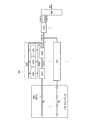
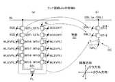
先ず、図1を参照して、第1の実施の形態に係る半導体記憶装置の概略構成について説明する。第1の実施の形態に係る半導体記憶装置は、図1に示すように、NAND型フラッシュメモリ等の不揮発性メモリ1と、そのビット線BL方向の両側に配置されたDRAM等の揮発性メモリ2とを有する。不揮発性メモリ1と揮発性メモリ2とは、後述するように、同様の三次元積層構造を有し、同一のプロセスで形成される。揮発性メモリ2は、不揮発性メモリ1のデータ書き込み及び読み出しの際に使用されるラッチ回路やページバッファ回路として使用される。この例では、不揮発性メモリ1がNAND型のセルアレイCAを構成し、揮発性メモリ2がセルアレイCAからのデータの書き込み及び読み出しの際のセンスアンプに接続されるラッチ回路LDL,UDL,SDLとして使用される。[First Embodiment]
[Schematic configuration]
First, a schematic configuration of the semiconductor memory device according to the first embodiment will be described with reference to FIG. As shown in FIG. 1, the semiconductor memory device according to the first embodiment includes a
図2は、揮発性メモリ2をラッチ回路として使用する具体例を示すブロック図である。この半導体記憶装置は、セルアレイCA、センスアンプユニットSU、ラッチ回路XDL、及び選択回路SWを有する。 FIG. 2 is a block diagram showing a specific example in which the
セルアレイCAは、いわゆるNAND型フラッシュメモリであり、データを電気的に記憶する複数のメモリストリングMSを有する。一列に並ぶメモリストリングMSは、1本のビット線BLを介して1つのセンスアンプユニットSUに接続される。メモリストリングMSは、直列接続された複数のメモリトランジスタMTrから構成される。 The cell array CA is a so-called NAND flash memory, and includes a plurality of memory strings MS that electrically store data. The memory strings MS arranged in a line are connected to one sense amplifier unit SU via one bit line BL. The memory string MS is composed of a plurality of memory transistors MTr connected in series.
センスアンプユニットSUは、バスDBUSを介してラッチ回路XDLに接続される。センスアンプユニットSUは、第1センスアンプSA1、第2センスアンプSA2、及びラッチ回路LDL、UDL、SDLを有する。 The sense amplifier unit SU is connected to the latch circuit XDL via the bus DBUS. The sense amplifier unit SU includes a first sense amplifier SA1, a second sense amplifier SA2, and latch circuits LDL, UDL, and SDL.
第1センスアンプSA1は、ビット線BLを介してメモリストリングMS(メモリトランジスタMTr)からデータを読み出す。また、第1センスアンプSA1は、書込データに基づきビット線BLの電圧を制御し、メモリトランジスタMTrにデータを書き込む。第2センスアンプSA2は、一対のビット線DBL、/DBLを介してラッチ回路LDL、UDL、SDLからデータを読み出し、そのデータをバスLBUSを介して第1センスアンプSA1に転送する。また、第2センスアンプアンプSA2は、データバスDBUSを介してラッチ回路XDLからデータを読み出す。ラッチ回路LDL、UDL、SDLは、いわゆるDRAM構造を有する。 The first sense amplifier SA1 reads data from the memory string MS (memory transistor MTr) via the bit line BL. The first sense amplifier SA1 controls the voltage of the bit line BL based on the write data, and writes the data to the memory transistor MTr. The second sense amplifier SA2 reads data from the latch circuits LDL, UDL, SDL via the pair of bit lines DBL, / DBL, and transfers the data to the first sense amplifier SA1 via the bus LBUS. The second sense amplifier amplifier SA2 reads data from the latch circuit XDL via the data bus DBUS. The latch circuits LDL, UDL, and SDL have a so-called DRAM structure.
ラッチ回路XDLは、データバスDBUS、XBUSを介して受け付けたデータを記憶する。選択回路SWは、外部信号IOを選択的にラッチ回路XDLに供給する。 The latch circuit XDL stores data received via the data buses DBUS and XBUS. The selection circuit SW selectively supplies the external signal IO to the latch circuit XDL.
次に、図3を参照して、セルアレイCAについて詳しく説明する。セルアレイCAは、図3に示すように、m個のメモリブロックMB(1)、…MB(m)を含む。なお、以下において、全てのメモリブロックMB(1)・・・(m)を総称する場合には、メモリブロックMBと記載する場合もある。 Next, the cell array CA will be described in detail with reference to FIG. As shown in FIG. 3, the cell array CA includes m memory blocks MB (1),... MB (m). In the following description, when all the memory blocks MB (1)... (M) are collectively referred to, they may be described as memory blocks MB.
各メモリブロックMBは、それぞれn行2列のマトリクス状に配列されたメモリユニットMU(1、1)〜MU(2、n)を有する。n行2列はあくまで一例であり、これに限定されるものではない。以下では、各メモリユニットMU(1、1)〜(2、n)を区別することなく、単にメモリユニットMUと記載する場合もある。 Each memory block MB has memory units MU (1, 1) to MU (2, n) arranged in a matrix of n rows and 2 columns. The n rows and 2 columns are merely examples, and the present invention is not limited to these. Hereinafter, the memory units MU (1, 1) to (2, n) may be simply referred to as memory units MU without being distinguished from each other.
メモリユニットMU(1、1)〜(2、n)の一端は、ビット線BL(1)〜(n)に接続され、メモリユニットMU(1、1)〜(2、n)の他端は、ソース線SLに接続される。ビット線BL(1)〜(n)は、ロウ方向に所定ピッチをもって、複数のメモリブロックMBを跨ぐようにカラム方向に延びる。以下では、全てのビット線BL(1)・・・BL(n)を総称する場合には、ビット線BLと記載する場合もある。 One ends of the memory units MU (1, 1) to (2, n) are connected to the bit lines BL (1) to (n), and the other ends of the memory units MU (1, 1) to (2, n) are Are connected to the source line SL. The bit lines BL (1) to (n) have a predetermined pitch in the row direction and extend in the column direction so as to straddle the plurality of memory blocks MB. Hereinafter, when all the bit lines BL (1)... BL (n) are collectively referred to, they may be referred to as bit lines BL.
メモリユニットMUは、メモリストリングMS、ソース側選択トランジスタSSTr、及びドレイン側選択トランジスタSDTrを有する。 The memory unit MU includes a memory string MS, a source side selection transistor SSTr, and a drain side selection transistor SDTr.
メモリストリングMSは、図3に示すように、直列接続されたメモリトランジスタMTr1〜8(メモリセル)、及びバックゲートトランジスタBTrを有する。メモリトランジスタMTr1〜4、MTr5〜8は、各々、直列接続される。バックゲートトランジスタBTrは、メモリトランジスタMTr4とメモリトランジスタMTr5との間に接続される。なお、後述する図7、8に示すように、メモリトランジスタMTr1〜8は、ロウ方向、カラム方向、及び積層方向(半導体基板に対して垂直方向)に3次元的に配列される。 As shown in FIG. 3, the memory string MS includes memory transistors MTr1 to 8 (memory cells) and a back gate transistor BTr connected in series. Memory transistors MTr1-4 and MTr5-8 are each connected in series. The back gate transistor BTr is connected between the memory transistor MTr4 and the memory transistor MTr5. 7 and 8 described later, the memory transistors MTr1 to MTr8 are three-dimensionally arranged in the row direction, the column direction, and the stacking direction (a direction perpendicular to the semiconductor substrate).
メモリトランジスタMTr1〜8は、その電荷蓄積層に電荷を蓄積することによってデータを保持する。バックゲートトランジスタBTrは、少なくともメモリストリングMSを動作の対象として選択した場合に導通状態とされる。 The memory transistors MTr1-8 retain data by accumulating charges in their charge accumulation layers. The back gate transistor BTr is rendered conductive when at least the memory string MS is selected as an operation target.
メモリブロックMB(1)〜(m)において、n行2列のマトリクス状に配列されたメモリトランジスタMTr1〜8のゲートには、各々、ワード線WL1〜8が共通に接続される。n行2列のバックゲートトランジスタBTrのゲートには、バックゲート線BGが共通に接続される。 In memory blocks MB (1) to (m), word lines WL1 to WL8 are commonly connected to gates of memory transistors MTr1 to MTr1 to 8 arranged in a matrix of n rows and 2 columns, respectively. A back gate line BG is commonly connected to the gates of the n rows and 2 columns of back gate transistors BTr.
ソース側選択トランジスタSSTrのドレインは、メモリストリングMSのソースに接続される。ソース側選択トランジスタSSTrのソースはソース線SLに接続される。各メモリブロックMBにおいてロウ方向に1列に並ぶn個のソース側選択トランジスタSSTrのゲートには、1本のソース側選択ゲート線SGS(1)又はSGS(2)が共通に接続される。なお、以下では、ソース側選択ゲート線SGS(1)、(2)を区別せず総称してソース側選択ゲート線SGSと称することもある。 The drain of the source side select transistor SSTr is connected to the source of the memory string MS. The source of the source side select transistor SSTr is connected to the source line SL. In each memory block MB, one source-side selection gate line SGS (1) or SGS (2) is commonly connected to the gates of n source-side selection transistors SSTr arranged in a row in the row direction. Hereinafter, the source side select gate lines SGS (1) and (2) may be collectively referred to as source side select gate lines SGS without distinction.
ドレイン側選択トランジスタSDTrのソースは、メモリストリングMSのドレインに接続される。ドレイン側選択トランジスタSDTrのドレインは、ビット線BLに接続される。各メモリブロックMBにおいてロウ方向に一列に並ぶn個のドレイン側選択トランジスタSDTrのゲートには、ドレイン側選択ゲート線SGD(1)又はSGD(2)が共通に接続される。なお、以下では、ドレイン側選択ゲート線SGD(1)、(2)を区別せず総称してドレイン側選択ゲート線SGDと称することもある。 The source of the drain side select transistor SDTr is connected to the drain of the memory string MS. The drain of the drain side select transistor SDTr is connected to the bit line BL. A drain-side selection gate line SGD (1) or SGD (2) is commonly connected to the gates of n drain-side selection transistors SDTr arranged in a line in the row direction in each memory block MB. Hereinafter, the drain side selection gate lines SGD (1) and (2) may be collectively referred to as the drain side selection gate line SGD without being distinguished from each other.
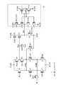
次に、図4を参照して、第1センスアンプSA1について詳しく説明する。図4に示すように、第1センスアンプSA1は、クランプ用トランジスタCT、nMOSトランジスタnT1〜nT7、pMOSトランジスタpT1〜pT4、キャパシタCAP、及びラッチ回路Laを有する。 Next, the first sense amplifier SA1 will be described in detail with reference to FIG. As shown in FIG. 4, the first sense amplifier SA1 includes a clamping transistor CT, nMOS transistors nT1 to nT7, pMOS transistors pT1 to pT4, a capacitor CAP, and a latch circuit La.
クランプ用トランジスタCTは、電流経路の一端がビット線BLに接続され、他端がノードCOM2に接続され、ゲートに電圧BLCが印加される。クランプ用トランジスタCTは、電圧BLC及びノードCOM2の電圧に基づいて決まる電圧をビット線BLに転送する。キャパシタCAPは、センスノードSENに接続される。電源ノードN_VDDとセンスノードSENの間には信号HLLで駆動されるプリチャージ用のMOSトランジスタnT3が接続される。センスノードSENとノードCOM1との間には、信号XXLで駆動される電荷転送用のMOSトランジスタnT2が接続される。電源ノードN_VDDとノードCOM1との間には、電流継続供給用のMOSトランジスタnT1が接続される。ノードCOM1とノードCOM2との間には、ラッチ回路Laにラッチされたデータによって駆動されるMOSトランジスタpT2,nT4が並列に接続される。ノードCOM2と接地ノードN_VSSの間には、MOSトランジスタpT2,nT4に対してオン/オフが反転した動作をするMOSトランジスタpT1,nT5が並列に接続される。セット用のトランジスタnT6は、セット信号SETに基づいてLBUSのデータをCOM1に転送する。 In the clamping transistor CT, one end of the current path is connected to the bit line BL, the other end is connected to the node COM2, and the voltage BLC is applied to the gate. The clamping transistor CT transfers a voltage determined based on the voltage BLC and the voltage of the node COM2 to the bit line BL. Capacitor CAP is connected to sense node SEN. A precharge MOS transistor nT3 driven by a signal HLL is connected between the power supply node N_VDD and the sense node SEN. A charge transfer MOS transistor nT2 driven by a signal XXL is connected between the sense node SEN and the node COM1. Between the power supply node N_VDD and the node COM1, a MOS transistor nT1 for continuous current supply is connected. Between the node COM1 and the node COM2, MOS transistors pT2 and nT4 driven by the data latched by the latch circuit La are connected in parallel. Between the node COM2 and the ground node N_VSS, the MOS transistors pT1 and nT5 which operate in an inverted manner with respect to the MOS transistors pT2 and nT4 are connected in parallel. The setting transistor nT6 transfers LBUS data to COM1 based on the set signal SET.
ゲートがセンスノードSENに接続されたMOSトランジスタpT3、MOSトランジスタpT3と電源ノードN_VDDとの間に接続されたストローブ信号STBnで駆動されるMOSトランジスタpT4及びMOSトランジスタpT3と接地ノードN_VSSとの間に接続されたリセット信号RST_CONで駆動されるMOSトランジスタnT7は、センスノードSENのレベルを弁別する弁別回路を構成する。この弁別回路の出力がラッチ回路LaのノードINVに入力される。 MOS transistor pT3 whose gate is connected to sense node SEN, MOS transistor pT4 driven by strobe signal STBn connected between MOS transistor pT3 and power supply node N_VDD, and connected between ground node N_VSS and MOS transistor pT3 The MOS transistor nT7 driven by the reset signal RST_CON thus configured constitutes a discrimination circuit that discriminates the level of the sense node SEN. The output of the discrimination circuit is input to the node INV of the latch circuit La.
ラッチ回路Laは、電源ノードN_VDD及び接地ノードN_VSSの間に相補対接続されたMOSトランジスタpT5,nT9からなるインバータと、同じくMOSトランジスタpT7,nT10からなるインバータとをクロスカップルして構成され、互いに逆論理となるノードINV,LATにデータを保持する。MOSトランジスタpT5,nT9には、直列にリセット信号RST_PCO及びストローブ信号STBnでそれぞれ駆動されるMOSトランジスタpT6,nT8が接続される。 The latch circuit La is configured by cross-coupled an inverter composed of MOS transistors pT5 and nT9 connected in a complementary pair between a power supply node N_VDD and a ground node N_VSS, and an inverter composed of MOS transistors pT7 and nT10, which are opposite to each other. Data is held in logical nodes INV and LAT. The MOS transistors pT5 and nT9 are connected in series with MOS transistors pT6 and nT8 that are respectively driven by a reset signal RST_PCO and a strobe signal STBn.
上記の構成において、データの書き込み時には、書き込みデータがラッチ回路Laに与えられる。選択ビット線BLに対応する第1センスアンプSA1ではノードINV=“H”、LAT=“L”とされる。よって、MOSトランジスタpT2、nT4が非導通状態、MOSトランジスタnT5、pT1が導通状態とされ、選択ビット線BLにはVSS(0V)が与えられる。非選択ビット線BLに対応する第1センスアンプSA1ではノードINV=“L”、LAT=“H”とされる。よって、MOSトランジスタnT5、pT1が非導通状態とされ、MOSトランジスタnT4、pT2が導通状態とされる。その結果、MOSトランジスタnT1によって、非選択ビット線BLは電源電圧VDDまで充電される。 In the above configuration, when data is written, write data is supplied to the latch circuit La. In the first sense amplifier SA1 corresponding to the selected bit line BL, the node INV = “H” and LAT = “L” are set. Therefore, the MOS transistors pT2 and nT4 are turned off, the MOS transistors nT5 and pT1 are turned on, and VSS (0 V) is applied to the selected bit line BL. In the first sense amplifier SA1 corresponding to the non-selected bit line BL, the node INV = “L” and LAT = “H” are set. Therefore, the MOS transistors nT5 and pT1 are turned off, and the MOS transistors nT4 and pT2 are turned on. As a result, the non-selected bit line BL is charged to the power supply voltage VDD by the MOS transistor nT1.
データの読み出し時には、MOSトランジスタnT1、MOSトランジスタpT2、nT4の電流経路、及びノードCOM1、COM2を介して、ビット線BLは所定電位まで充電される。また、MOSトランジスタnT3により、キャパシタCAPが充電され、センスノードSENの電位は電源電圧N_VDD近くまで上昇する。 At the time of reading data, the bit line BL is charged to a predetermined potential via the current path of the MOS transistor nT1, the MOS transistors pT2 and nT4, and the nodes COM1 and COM2. Further, the capacitor CAP is charged by the MOS transistor nT3, and the potential of the sense node SEN rises to near the power supply voltage N_VDD.
ここで、MOSトランジスタnT2をオン状態にすると、選択メモリトランジスタのデータに応じてビット線BLに電流が流れ、センスノードSENの電圧を変化させる。したがって、センスノードSENの電圧を検出することにより、選択メモリトランジスタからデータを読み出すことができる。すなわち、選択メモリトランジスタが導通状態であれば、センスノードSENの電位は低下し、MOSトランジスタpT3は導通状態となる。その結果、ノードINVは“H”、ノードLATは“L”となる。そして、MOSトランジスタpT1、nT5が導通状態となり、ビット線BLはVSS(0V)に固定される。他方、選択メモリトランジスタが非導通状態であれば、センスノードSENの電位は低下せず、MOSトランジスタpT3は非導通状態である。よって、ノードINVは“L”、ノードLATは“H”を維持する。この場合、MOSトランジスタnT1,pT2,nT4を介してビット線BLへの電流供給を継続する。 Here, when the MOS transistor nT2 is turned on, a current flows through the bit line BL according to the data of the selected memory transistor, and the voltage of the sense node SEN is changed. Therefore, data can be read from the selected memory transistor by detecting the voltage of the sense node SEN. That is, if the selected memory transistor is in a conductive state, the potential of the sense node SEN is lowered and the MOS transistor pT3 is in a conductive state. As a result, the node INV becomes “H” and the node LAT becomes “L”. Then, the MOS transistors pT1 and nT5 are turned on, and the bit line BL is fixed at VSS (0V). On the other hand, if the selected memory transistor is non-conductive, the potential of the sense node SEN does not decrease, and the MOS transistor pT3 is non-conductive. Therefore, the node INV maintains “L” and the node LAT maintains “H”. In this case, current supply to the bit line BL is continued through the MOS transistors nT1, pT2, and nT4.
次に、図5を参照して、ラッチ回路LDL、及び第2センスアンプSA2について詳しく説明する。なお、図5はラッチ回路LDLのみを示すが、ラッチ回路UDL、SDLもラッチ回路LDLと同様の構成を有する。 Next, the latch circuit LDL and the second sense amplifier SA2 will be described in detail with reference to FIG. FIG. 5 shows only the latch circuit LDL, but the latch circuits UDL and SDL have the same configuration as the latch circuit LDL.
図5に示すように、ラッチ回路LDLはペアセルを構成するメモリセルDCを有する。メモリセルDCは、トランジスタDTr、キャパシタC、及び端子ETを含むDRAM構造を有する。メモリセルDCは、トランジスタDTrを選択的に導通/非導通状態とし、キャパシタCにデータを書き込み又はキャパシタCからデータを読み出す。ビット線DBLに接続されたメモリセルDCとビット線/DBLに接続されたメモリセルDCとは、互いに異なるデータを記憶し、同一のワード線DWLによって駆動される。キャパシタCの一端はトランジスタDTrを介してビット線DBL又は/DBLに接続され、他端は所定の固定電位を与えられた端子ETに接続される。 As shown in FIG. 5, the latch circuit LDL has memory cells DC that constitute a pair cell. The memory cell DC has a DRAM structure including a transistor DTr, a capacitor C, and a terminal ET. The memory cell DC selectively turns on / off the transistor DTr and writes data to the capacitor C or reads data from the capacitor C. The memory cell DC connected to the bit line DBL and the memory cell DC connected to the bit line / DBL store different data and are driven by the same word line DWL. One end of the capacitor C is connected to the bit line DBL or / DBL via the transistor DTr, and the other end is connected to a terminal ET to which a predetermined fixed potential is applied.
図5に示すように、第2センスアンプSA2は、差動アンプS/A、イコライザBLE、カラム選択用のトランジスタTr1、/Tr1、及びバス選択用のトランジスタLBSW、DBSWを有する。 As shown in FIG. 5, the second sense amplifier SA2 includes a differential amplifier S / A, an equalizer BLE, column selection transistors Tr1 and / Tr1, and bus selection transistors LBSW and DBSW.
差動アンプS/Aは、駆動信号SAN、SAPによって動作し、データに対応したビット線DBL、/DBLの電位差を増幅する。イコライザBLEは、センス動作に先立って、信号BQLに応じて、ビット線DBL、/DBLを中間電位電圧VBLに固定する。トランジスタTr1、/Tr1は、選択カラム線CSLによって駆動され、ビット線DBL、/DBLの電圧を差動アンプS/Aに転送する。 The differential amplifier S / A operates in accordance with the drive signals SAN and SAP, and amplifies the potential difference between the bit lines DBL and / DBL corresponding to the data. Prior to the sensing operation, the equalizer BLE fixes the bit lines DBL and / DBL to the intermediate potential voltage VBL according to the signal BQL. The transistors Tr1 and / Tr1 are driven by the selected column line CSL and transfer the voltages of the bit lines DBL and / DBL to the differential amplifier S / A.
トランジスタLBSW、DBSWは、ビット線DBLとバスLBUS,DBSUとをそれぞれ接続する。 The transistors LBSW and DBSW connect the bit line DBL and the buses LBUS and DBSU, respectively.
[動作]
図6を参照して、ラッチ回路LDL、UDL、SDLに対する読出動作、及び書込動作について説明する。[Operation]
With reference to FIG. 6, a read operation and a write operation for latch circuits LDL, UDL, and SDL will be described.
先ず、図6(a)参照して読出動作について説明する。図6(a)に示すように、時刻t11にて、選択ワード線DWLの電位が上がると、ビット線対DBL、/DBLの間には、選択ワード線DWLに繋がるメモリセルDCのデータ(“0”又は“1”)に応じた電位差が発生する。図6(a)に示すように、ビット線DBLの電圧は、“1”データの場合に、キャパシタCからの放電によって上昇する。一方、ビット線DBLの電圧は、“0”データの場合にキャパシタCへと充電されるため低下する。次に、時刻t12にて、選択カラム線CSLの電圧を上げて差動アンプS/Aによってビット線対DBL、/DBLの間の電位差が(メモリセルDCのデータ)が読み出される。この後、時刻t13にて、選択ワード線DWLの電位を下げる。 First, the reading operation will be described with reference to FIG. As shown in FIG. 6A, when the potential of the selected word line DWL rises at time t11, the data ("" of the memory cell DC connected to the selected word line DWL is interposed between the bit line pair DBL and / DBL. A potential difference corresponding to “0” or “1”) is generated. As shown in FIG. 6A, the voltage of the bit line DBL rises due to the discharge from the capacitor C in the case of “1” data. On the other hand, the voltage of the bit line DBL decreases because the capacitor C is charged in the case of “0” data. Next, at time t12, the voltage of the selected column line CSL is increased, and the potential difference between the bit line pair DBL and / DBL (data of the memory cell DC) is read by the differential amplifier S / A. Thereafter, at time t13, the potential of the selected word line DWL is lowered.
次に、図6(b)を参照して書込動作について説明する。図6(b)に示すように、時刻t21にて、選択ワード線DWLの電位が上がると、ビット線対DBL、/DBLの間には、選択ワード線DWLに繋がるメモリセルDCのデータ(“0”又は“1”)に応じた電位差が発生する。次に、時刻t22にて、選択カラム線CSLの電圧を上げる。このとき、トランジスタDBSWを介してDBUSからビット線DBLに書き込みデータが転送される。このため、トランジスタTr1,/Tr1を介してメモリセルDCが接続されたビット線対DBL、/DBLに書き込みデータが転送され、メモリセルDCにデータを書き込む。図示の例では、メモリセルDCのデータを“1”から“0”に書き換える場合を示しており、ビット線DBLの電圧が“L”レベルなので、ビット線DBLに接続されたメモリセルDCのキャパシタCの電荷は放電されてデータが反転する。一方、ビット線/DBL側では、メモリセルDCのデータが“0”から“1”に書き換えられる。この場合、ビット線/DBLの電圧により、そのビット線/DBLに接続されたメモリセルDCのキャパシタCが充電される。この後、時刻t23にて、選択ワード線DWLの電位を下げる。 Next, the writing operation will be described with reference to FIG. As shown in FIG. 6B, when the potential of the selected word line DWL rises at time t21, the data ("" of the memory cell DC connected to the selected word line DWL is interposed between the bit line pair DBL and / DBL. A potential difference corresponding to “0” or “1”) is generated. Next, at time t22, the voltage of the selected column line CSL is increased. At this time, write data is transferred from DBUS to the bit line DBL via the transistor DBSW. Therefore, the write data is transferred to the bit line pair DBL, / DBL to which the memory cell DC is connected via the transistors Tr1, / Tr1, and the data is written to the memory cell DC. In the example shown in the figure, data in the memory cell DC is rewritten from “1” to “0”. Since the voltage of the bit line DBL is “L” level, the capacitor of the memory cell DC connected to the bit line DBL is shown. The charge of C is discharged and the data is inverted. On the other hand, on the bit line / DBL side, the data in the memory cell DC is rewritten from “0” to “1”. In this case, the capacitor C of the memory cell DC connected to the bit line / DBL is charged by the voltage of the bit line / DBL. Thereafter, at time t23, the potential of the selected word line DWL is lowered.
[積層構造]
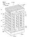
次に、本実施の形態に係る半導体記憶装置の積層構造について具体的に説明する。図7は、セルアレイCA、及びラッチ回路LDLの斜視図であり、図8は、セルアレイCA、及びラッチ回路LDLの断面図である。なお、以下の説明は、ラッチ回路LDLのみとなるが、ラッチ回路UDL、SDLは、ラッチ回路LDLと同様の構造を有する。[Laminated structure]
Next, the stacked structure of the semiconductor memory device according to this embodiment will be specifically described. FIG. 7 is a perspective view of the cell array CA and the latch circuit LDL, and FIG. 8 is a cross-sectional view of the cell array CA and the latch circuit LDL. In the following description, only the latch circuit LDL is described, but the latch circuits UDL and SDL have the same structure as the latch circuit LDL.
セルアレイCAは、図7及び図8に示すように、半導体基板20上に順次積層されたバックゲート層30、メモリ層40、選択トランジスタ層50、及び配線層60を有する。バックゲート層30にはバックゲートトランジスタBTrが形成される。メモリ層40にはメモリトランジスタMTr1〜8が形成される。選択トランジスタ層50にはドレイン側選択トランジスタSDTr及びソース側選択トランジスタSSTrが形成される。配線層60にはソース線SL及びビット線BLが形成される。 As shown in FIGS. 7 and 8, the cell array CA includes a
バックゲート層30は、図7及び図8に示すように、バックゲート導電層31を有する。バックゲート導電層31は、例えばポリシリコン(poly−Si)にて形成され、バックゲート線BG、及びバックゲートトランジスタBTrのゲートとして機能する。バックゲート導電層31は、半導体基板20と平行なロウ方向及びカラム方向に2次元的に広がるように形成される。 The
また、バックゲート層30は、図8に示すように、メモリゲート絶縁層32、及び半導体層33を有する。半導体層33はバックゲートトランジスタBTrのボディ(チャネル)として機能する。 Further, the
メモリゲート絶縁層32は、バックゲート導電層31の側面に接する。半導体層33は、バックゲート導電層31と共にメモリゲート絶縁層32を挟む。すなわち、バックゲート導電層31は、メモリゲート絶縁層32を介して半導体層33の側面及び下面を取り囲む。 The memory
半導体層33はバックゲートトランジスタBTrのボディ(チャネル)として機能し、バックゲート導電層31を掘り込むように形成される。半導体層33は、例えばポリシリコン(poly−Si)にて、上面からみてカラム方向を長手方向とする略矩形状に形成され、1つのメモリブロックMB中でロウ方向及びカラム方向にマトリクス状に形成される。 The
メモリ層40は、図7及び図8に示すように、バックゲート層30の上層に形成される。メモリ層40は、4層のワード線導電層41a〜41dを有する。ワード線導電層41aは、ワード線WL4,WL5及びメモリトランジスタMTr4,MTr5のゲートとして機能する。同様に、ワード線導電層41b〜41dは、各々、ワード線WL1〜3,WL6〜8及びメモリトランジスタMTr1〜3,MTr6〜8のゲートとして機能する。 The
ワード線導電層41a〜41dは、その上下間に層間絶縁層を挟んで積層される。ワード線導電層41a〜41dは、例えばポリシリコン(poly−Si)にて、カラム方向にピッチをもってロウ方向を長手方向として延びるように形成される。 The word line
メモリ層40は、図8に示すように、メモリゲート絶縁層43、及び柱状半導体層44を有する。柱状半導体層44は、メモリトランジスタMTr1〜8のボディ(チャネル)として機能する。 As shown in FIG. 8, the
メモリゲート絶縁層43は、柱状半導体層44とワード線導電層41a〜41dの間に、上述したメモリゲート絶縁層32と連続して一体に形成される。メモリゲート絶縁層43は、ワード線導電層41a〜41dの側面側から柱状半導体層44側へと、それぞれ所定の厚みを持ったブロック絶縁層43a、電荷蓄積層43b、及びトンネル絶縁層43cを有する。電荷蓄積層43bは、電荷を蓄積可能に構成される。ブロック絶縁層43a及びトンネル絶縁層43cは、例えば酸化シリコン(SiO2)にて構成される。電荷蓄積層43bは、例えば窒化シリコン(SiN)にて構成される。The memory
柱状半導体層44は、ワード線導電層41a〜41dを貫通する。すなわち、ワード線導電層41a〜41dは、メモリゲート絶縁層43を介して柱状半導体層44の側面を取り囲む。柱状半導体層44は、半導体基板20に対して垂直方向に延びる。一対の柱状半導体層44は、上述した半導体層33と連続的に一体形成され、半導体層33のカラム方向の端部近傍に整合する。柱状半導体層44は、例えばポリシリコン(poly−Si)にて構成される。 The
上記バックゲート層30、及びメモリ層40において、一対の柱状半導体層44、及びその下端を連結する半導体層33は、メモリストリングMSのボディ(チャネル)として機能するメモリ半導体層44Aを構成する。メモリ半導体層44Aは、ロウ方向からみてU字状に形成される。 In the
選択トランジスタ層50は、図7及び図8に示すように、ソース側導電層51a、及びドレイン側導電層51bを有する。ソース側導電層51aは、ソース側選択ゲート線SGS、及びソース側選択トランジスタSSTrのゲートとして機能する。ドレイン側導電層51bは、ドレイン側選択ゲート線SGD、及びドレイン側選択トランジスタSDTrのゲートとして機能する。 As shown in FIGS. 7 and 8, the
ソース側導電層51aは、メモリ半導体層44Aを構成する一方の柱状半導体層44の上層に形成される。ドレイン側導電層51bは、ソース側導電層51aと同層であって、メモリ半導体層44Aを構成する他方の柱状半導体層44の上層に形成される。複数のソース側導電層51a、及びドレイン側導電層51bは、例えばポリシリコン(poly−Si)にて、カラム方向に所定ピッチをもってロウ方向に延びるように形成される。 The source side
選択トランジスタ層50は、図8に示すように、ソース側ゲート絶縁層52a、ソース側柱状半導体層53a、ドレイン側ゲート絶縁層52b、及びドレイン側柱状半導体層53bを有する。ソース側柱状半導体層53aはソース側選択トランジスタSSTrのボディ(チャネル)として機能する。ドレイン側柱状半導体層53bはドレイン側選択トランジスタSDTrのボディ(チャネル)として機能する。 As shown in FIG. 8, the
ソース側ゲート絶縁層52aは、例えば酸化シリコン(SiO2)にて、ソース側導電層51aの側面に接するように形成される。The source side
ソース側柱状半導体層53aは、ソース側導電層51aと共にソース側ゲート絶縁層52aを挟む。ソース側柱状半導体層53aはソース側導電層51aを貫通する。すなわち、ソース側導電層51aは、ソース側ゲート絶縁層52aを介してソース側柱状半導体層53aの側面を取り囲む。ソース側柱状半導体層53aは、一対の柱状半導体層44の一方の上面に接続され、半導体基板20に対して垂直方向に延びる柱状に形成される。ソース側柱状半導体層53aは、例えばポリシリコン(poly−Si)にて構成される。 The source side
ドレイン側ゲート絶縁層52bは、例えば酸化シリコン(SiO2)にて、ドレイン側導電層51bの側面に接するように形成される。The drain side
ドレイン側柱状半導体層53bは、ドレイン側導電層51bと共にドレイン側ゲート絶縁層52bを挟む。ドレイン側柱状半導体層53bは、ドレイン側導電層51bを貫通する。すなわち、ドレイン側導電層51bは、ドレイン側ゲート絶縁層52bを介してドレイン側柱状半導体層53bの側面を取り囲む。ドレイン側柱状半導体層53bは、一対の柱状半導体層44の一方の上面に接続され、半導体基板20に対して垂直方向に延びる柱状に形成される。ドレイン側柱状半導体層53bは、例えばポリシリコン(poly−Si)にて構成される。 The drain side
配線層60は、ソース線層61、ビット線層62、及びプラグ層63を有する。ソース線層61はソース線SLとして機能する。ビット線層62はビット線BLとして機能する。 The
ソース線層61は、ソース側柱状半導体層53aの上面に接し、ロウ方向に延びる。ビット線層62は、プラグ層63を介してドレイン側柱状半導体層53bの上面に接し、カラム方向に延びる。ソース線層61、ビット線層62、及びプラグ層63は、例えばタングステン等の金属にて構成される。 The
次に、ラッチ回路LDLについて説明する。ラッチ回路LDLは、図7及び図8に示すように、セルアレイCAと同様の積層構造を有する。すなわち、ラッチ回路LDLは、セルアレイCAと同様に、バックゲート層30、メモリ層40、選択トランジスタ層50、及び配線層60を有する。ラッチ回路LDLは、図1に示すように、セルアレイCAにビット線BLの伸びる方向に隣接させて形成される。ラッチ回路LDLに接続されるビット線DBL、/DBLは、セルアレイCAのビット線BLと同一ピッチである。 Next, the latch circuit LDL will be described. As shown in FIGS. 7 and 8, the latch circuit LDL has a stacked structure similar to that of the cell array CA. That is, the latch circuit LDL includes the
なお、ラッチ回路LDL内のバックゲート導電層31は、セルアレイCA内のバックゲート導電層31と同層に形成される。ラッチ回路LDL内のワード線導電層41a〜41dは、セルアレイCA内のワード線導電層41a〜41dと同層に形成される。ラッチ回路LDL内のソース側導電層51a及びドレイン側導電層51bは、セルアレイCA内のソース側導電層51a及びドレイン側導電層51bと同層に形成される。 Note that the back gate
第1、第2センスアンプSA1、SA2は、図8に示すように、ラッチ回路LDLの下層に位置し、半導体基板20上に形成される。第1、第2センスアンプSA1、SA2は、各々、積層方向に延びるコンタクト81を介してビット線層62と電気的に接続される。 As shown in FIG. 8, the first and second sense amplifiers SA1 and SA2 are located on the lower layer of the latch circuit LDL and are formed on the
第1、第2センスアンプSA1、SA2は、各々、一対の拡散層82、ゲート絶縁層83、及び導電層84を有する。一対の拡散層82は、各々、半導体基板20の表面に形成され、トランジスタのソース・ドレインとして機能する。一対の拡散層82の一方は、プラグ層85及び配線層86を介してコンタクト81に接続される。ゲート絶縁層83は、各々、一対の拡散層82を跨ぐように半導体基板20上に形成される。導電層84は、ゲート絶縁層83上に形成され、トランジスタのゲートとして機能する。 The first and second sense amplifiers SA1 and SA2 each have a pair of diffusion layers 82, a
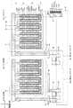
上記積層構造により、図8に示すセルアレイCAの領域Aは、図9に示すメモリユニットMU(メモリストリングMS、ソース側選択トランジスタSSTr、ドレイン側選択トランジスタSDTr)として機能する。図9に示すように、メモリストリングMSは、ロウ方向からみてU字状に曲がる。各種トランジスタMTr1〜8、BTr、SSTr、SDTrのゲートに印加される電圧は、各々独立に制御される。これにより、各種トランジスタMTr1〜8、BTr、SSTr、SDTrは導通状態又は非導通状態とされ、メモリトランジスタMTr1〜8に対してデータの書込、読出、消去が実行される。 With the stacked structure, the region A of the cell array CA illustrated in FIG. 8 functions as the memory unit MU (memory string MS, source-side selection transistor SSTr, drain-side selection transistor SDTr) illustrated in FIG. As shown in FIG. 9, the memory string MS bends in a U shape when viewed from the row direction. The voltages applied to the gates of the various transistors MTr1-8, BTr, SSTr, SDTr are controlled independently. As a result, the various transistors MTr1-8, BTr, SSTr, SDTr are rendered conductive or non-conductive, and data is written, read, and erased from / to the memory transistors MTr1-8.
また、上記積層構造により、図8に示すラッチ回路LDLの領域Bは、図10(a)に示すメモリユニットMUとして機能し得る。しかしながら、ラッチ回路LDLにおいて、メモリトランジスタMTr1〜8のゲート、バックゲートトランジスタBTrのゲートには固定電位VPLが供給される。固定電位VPLとしては、メモリトランジスタMTr1をオン状態にする電圧が、チャネル容量を増加させ得るという点で望ましい。そして、ソース側選択トランジスタSDTrは、ゲート電圧により常に非導通状態(OFF)に制御され、ソース側柱状半導体層53aとソース線層61は電気的に非接続となる。これら制御により、図8に示すラッチ回路LDLの領域Bは、図10(b)に示すメモリセルDC(DRAM)として機能する。すなわち、メモリストリングMS(メモリトランジスタMTr1〜8、バックゲートトランジスタBTr)のボディは、図10(b)に示すようにメモリセルDCのキャパシタCとして機能する。メモリトランジスタMTr1〜8、バックゲートトランジスタBTrのゲートは、キャパシタCの一端に固定電位を供給する端子ETとして機能する。ドレイン側選択トランジスタSDTrは、メモリセルDCの動作に応じて導通/非導通状態に制御されるトランジスタDTrとして機能し、ドレイン側選択ゲート線SGDは、ワード線DWLとして機能する。ビット線BLは、ビット線DBL(又は/DBL)として機能する。 Further, due to the stacked structure, the region B of the latch circuit LDL shown in FIG. 8 can function as the memory unit MU shown in FIG. However, in the latch circuit LDL, the fixed potential VPL is supplied to the gates of the memory transistors MTr1-8 and the gate of the back gate transistor BTr. As the fixed potential VPL, a voltage for turning on the memory transistor MTr1 is desirable in that the channel capacitance can be increased. The source side select transistor SDTr is always controlled to be in a non-conductive state (OFF) by the gate voltage, and the source side
また、図8に示したラッチ回路LDLの積層構造は、以下のように機能する。すなわち、ラッチ回路LDLにおいて、ドレイン側柱状半導体層53bは、トランジスタDTrのボディとして機能する。ドレイン側導電層51bは、トランジスタDTrのゲート、及びワード線DWLとして機能する。メモリ半導体層44Aは、キャパシタCとして機能する。バックゲート導電層31、ワード線導電層41a〜41dは、キャパシタCの一端に接続された端子ETとして機能する。 The stacked structure of the latch circuit LDL shown in FIG. 8 functions as follows. That is, in the latch circuit LDL, the drain side
次に、図11を参照して、比較例と本実施の形態とを比較する。図11は、比較例に係る半導体記憶装置の断面図である。図11に示すように、比較例において、第1、第2センスアンプSA1、SA2、及びラッチ回路LDLは、セルアレイCAの下層に位置する。比較例に係るラッチ回路LDLにおいて、メモリセルDCのトランジスタDTrは、半導体基板20上にチャネルを有する。メモリセルDCのキャパシタCは、一般的なトレンチ構造、又はスタック構造を有する(図示略)。 Next, referring to FIG. 11, a comparative example and this embodiment are compared. FIG. 11 is a cross-sectional view of a semiconductor memory device according to a comparative example. As shown in FIG. 11, in the comparative example, the first and second sense amplifiers SA1 and SA2 and the latch circuit LDL are located below the cell array CA. In the latch circuit LDL according to the comparative example, the transistor DTr of the memory cell DC has a channel on the
上記のような比較例に対し、本実施の形態のラッチ回路LDLによれば、メモリセルDCのキャパシタCを、積層方向に延びるメモリ半導体層44Aにて構成することができる。これにより、比較例と比べてセルアレイCAのメモリセルピッチが微小になっても、十分な容量を確保することができる。すなわち、第1の実施の形態に係るラッチ回路LDLは、半導体基板20内にラッチ回路LDL,UDL,SDLを形成する比較例よりも遙かに占有面積を縮小化でき、且つ実行面積を増大することができる。 In contrast to the comparative example as described above, according to the latch circuit LDL of the present embodiment, the capacitor C of the memory cell DC can be configured by the
また、本実施の形態において、ラッチ回路LDLは、セルアレイCAと同層に位置し、第1、第2センスアンプSA1、SA2は、ラッチ回路LDL,UDL,SDLの下層に位置する。これにより、第1の実施の形態は、比較例よりもセルアレイCAの下層にスペースを確保でき、そのスペースに他の回路を配置できる。また、セルアレイCAとラッチ回路LDL,UDL,SDLとは、同一のプロセスで形成することができる。 In the present embodiment, the latch circuit LDL is located in the same layer as the cell array CA, and the first and second sense amplifiers SA1 and SA2 are located under the latch circuits LDL, UDL, and SDL. Thereby, the first embodiment can secure a space below the cell array CA than the comparative example, and can arrange other circuits in the space. The cell array CA and the latch circuits LDL, UDL, SDL can be formed by the same process.
[第2の実施の形態]
次に、図12を参照して、第2の実施の形態に係る半導体記憶装置を説明する。図12は、ラッチ回路LDLの積層構造のみを示す。なお、第2の実施の形態において、セルアレイCAの積層構造は第1の実施の形態と同様である。[Second Embodiment]
Next, a semiconductor memory device according to the second embodiment will be described with reference to FIG. FIG. 12 shows only the laminated structure of the latch circuit LDL. In the second embodiment, the stacked structure of the cell array CA is the same as that of the first embodiment.
図12に示すように、第2の実施の形態に係るラッチ回路LDLは、ワード線導電層41a〜41dの代わりに、1層のワード線導電層41を有する。ワード線導電層41は、セルアレイCA内のワード線導電層41aの下端の位置からワード線導電層41dの上端の位置まで連続的に形成される。 As shown in FIG. 12, the latch circuit LDL according to the second embodiment includes a single word line conductive layer 41 instead of the word line
上記のワード線導電層41は、ワード線導電層41a〜41dよりもメモリ半導体層44Aとの間の容量を大きくできる。これにより、第2の実施の形態は、第1の実施の形態よりもメモリセルDCのデータリテンションを向上させる。また、第2の実施の形態は、第1の実施の形態よりも製造工程を簡略化できる。 The capacitance between the word line conductive layer 41 and the
[第3の実施の形態]
次に、図13を参照して、第3の実施の形態に係る半導体記憶装置を説明する。図13は、ラッチ回路LDLの積層構造のみを示す。なお、第3の実施の形態において、セルアレイCAの積層構造は第1の実施の形態と同様である。[Third Embodiment]
Next, a semiconductor memory device according to the third embodiment will be described with reference to FIG. FIG. 13 shows only the laminated structure of the latch circuit LDL. In the third embodiment, the stacked structure of the cell array CA is the same as that of the first embodiment.
図13に示すように、第3の実施の形態に係るラッチ回路LDLにおいて、ソース側柱状半導体層53aは、ソース線層61から物理的に分断される。これにより、第3の実施の形態においては、第1の実施の形態のように、ラッチ回路LDLにおいてソース側選択トランジスタSSTrを非導通状態に制御する必要はない。また、キャパシタCからソース線層61へのリーク電流を抑制することができる。 As shown in FIG. 13, in the latch circuit LDL according to the third embodiment, the source-side
[第4の実施の形態]
次に、図14を参照して、第4の実施の形態に係る半導体記憶装置を説明する。図14は、ラッチ回路LDLの回路構成を示す。なお、第4の実施の形態において、セルアレイCAの回路構成は第1の実施の形態と同様である。[Fourth Embodiment]
Next, a semiconductor memory device according to the fourth embodiment will be described with reference to FIG. FIG. 14 shows a circuit configuration of the latch circuit LDL. In the fourth embodiment, the circuit configuration of the cell array CA is the same as that of the first embodiment.
図14(a)、(b)に示すように、第4の実施の形態に係るメモリセルDCは、キャパシタに直列接続された2つのトランジスタDTr1、DTr2を有し、この点で第1の実施の形態と異なる。 As shown in FIGS. 14A and 14B, the memory cell DC according to the fourth embodiment has two transistors DTr1 and DTr2 connected in series to a capacitor. The form is different.
図14に示す構成は、例えば、選択トランジスタ層50を2層積層させること、又は上層のメモリトランジスタMTriをメモリトランジスタDTrとして使用することにより実現される。直列接続されたトランジスタDTr1、DTr2により、ビット線DBL(又は/DBL)からキャパシタCへのリーク電流を第1の実施の形態よりも抑制できる。直列接続するトランジスタDTrの数は2つに限定されるものではなく、更に増やすようにしても良い。 The configuration shown in FIG. 14 is realized, for example, by stacking two select transistor layers 50 or using the upper memory transistor MTri as the memory transistor DTr. The leakage current from the bit line DBL (or / DBL) to the capacitor C can be suppressed as compared with the first embodiment by the transistors DTr1 and DTr2 connected in series. The number of transistors DTr connected in series is not limited to two, and may be further increased.
[その他]
本発明のいくつかの実施の形態を説明したが、これらの実施の形態は、例として提示したものであり、発明の範囲を限定することは意図していない。これら新規な実施の形態は、その他の様々な形態で実施されることが可能であり、発明の要旨を逸脱しない範囲で、種々の省略、置き換え、変更を行うことができる。これら実施の形態やその変形は、発明の範囲や要旨に含まれるとともに、特許請求の範囲に記載された発明とその均等の範囲に含まれる。[Others]
Although several embodiments of the present invention have been described, these embodiments are presented as examples and are not intended to limit the scope of the invention. These novel embodiments can be implemented in various other forms, and various omissions, replacements, and changes can be made without departing from the scope of the invention. These embodiments and modifications thereof are included in the scope and gist of the invention, and are included in the invention described in the claims and the equivalents thereof.
1…不揮発性メモリ、 2…揮発性メモリ、 CA…セルアレイ、 XDL、LDL、UDL、SDL…ラッチ回路、 SA1…第1センスアンプ、 SA2…第2センスアンプ、 MB…メモリブロック、 MU…メモリユニット、 MS…メモリストリング、 MTr1〜8…メモリトランジスタ、 SSTr…ソース側選択トランジスタ、 SDTr…ドレイン側選択トランジスタ、 BTr…バックゲートトランジスタ、 DC…メモリセル、 DTr…トランジスタ、 C…キャパシタ。 DESCRIPTION OF
Claims (8)
Translated fromJapanese前記不揮発性メモリは、
電気的に書き換え可能な複数の第1メモリトランジスタを積層構造により直列接続してなる複数の第1メモリストリング及びその両端に一端を接続された第1及び第2選択トランジスタを有する第1メモリユニットと、
前記第1選択トランジスタの他端に接続された第1ビット線と、
前記メモリトランジスタのゲートに接続された第1ワード線と、
前記第1及び第2選択トランジスタのゲートに接続された制御ゲート線と、
前記第2選択トランジスタの他端に接続されたソース線とを備え、
前記第1メモリストリングは、
基板に対して垂直方向に延びる第1柱状部を含み、前記第1メモリトランジスタのボディとして機能する第1半導体層と、
前記第1柱状部の側面を取り囲むように形成されて、電荷を蓄積可能に構成された第1電荷蓄積層と、
前記第1電荷蓄積層を介して前記第1柱状部の側面を取り囲むように形成され、前記第1メモリトランジスタのゲートとして機能する複数の第1導電層とを有し、
前記揮発性メモリは、
電気的に書き換え可能な複数の第2メモリトランジスタを積層構造により直列接続してなる複数の第2メモリストリング及びその両端に一端を接続された第3及び第4選択トランジスタを有する第2メモリユニットと、
前記第3選択トランジスタの他端に接続された第2ビット線と、
前記第3選択トランジスタのゲートに接続された第2ワード線と、
前記第4選択トランジスタの他端側に設けられた第2ソース線とを備え、
前記第2メモリストリングは、
前記基板に対して垂直方向に延びる第2柱状部を含み、前記第2メモリトランジスタのボディとして機能する第2半導体層と、
前記第2柱状部の側面を取り囲むように形成されて、電荷を蓄積可能に構成された第2電荷蓄積層と、
前記第2電荷蓄積層を介して前記第2柱状部の側面を取り囲むように形成され、前記第2メモリトランジスタのゲートとして機能する第2導電層とを有し、
前記第2メモリトランジスタのゲートは、所定の固定電位を供給され、
前記第2半導体層はキャパシタとして機能し、
前記第2半導体層と前記第2ソース線とは非接続とされ、
前記センスアンプは、前記基板上に形成され、
前記揮発性メモリと前記センスアンプとが前記第2ビット線を介して接続され、
前記揮発性メモリは、前記不揮発性メモリに前記第1ビット線の延びる方向に隣接させて形成され、
1本の前記第1ビット線に対して2本の前記第2ビット線が対応する
ことを特徴とする半導体記憶装置。A nonvolatile memory, a volatile memory, and a sense amplifier;
The nonvolatile memory is
A first memory unit having a plurality of first memory strings in which a plurality of electrically rewritable first memory transistors are connected in series in a stacked structure, and first and second select transistors having one ends connected to both ends thereof; ,
A first bit line connected to the other end of the first select transistor;
A first word line connected to the gate of the memory transistor;
A control gate line connected to the gates of the first and second select transistors;
A source line connected to the other end of the second selection transistor,
The first memory string is:
A first semiconductor layer including a first columnar portion extending in a direction perpendicular to the substrate and functioning as a body of the first memory transistor;
A first charge storage layer formed so as to surround a side surface of the first columnar part and configured to be capable of storing charges;
A plurality of first conductive layers formed so as to surround a side surface of the first columnar portion via the first charge storage layer, and functioning as gates of the first memory transistor;
The volatile memory is
A second memory unit having a plurality of second memory strings in which a plurality of electrically rewritable second memory transistors are connected in series in a stacked structure, and third and fourth select transistors having one ends connected to both ends thereof; ,
A second bit line connected to the other end of the third select transistor;
A second word line connected to the gate of the third select transistor;
A second source line provided on the other end side of the fourth select transistor,
The second memory string is
A second semiconductor layer including a second columnar portion extending in a direction perpendicular to the substrate and functioning as a body of the second memory transistor;
A second charge storage layer formed so as to surround a side surface of the second columnar part and configured to be capable of storing charges;
A second conductive layer formed so as to surround a side surface of the second columnar portion via the second charge storage layer and functioning as a gate of the second memory transistor;
A gate of the second memory transistor is supplied with a predetermined fixed potential;
The second semiconductor layer functions as a capacitor;
The second semiconductor layer and the second source line are disconnected;
The sense amplifier is formed on the substrate,
The volatile memory and the sense amplifier are connected via the second bit line,
The volatile memory is formed adjacent to the nonvolatile memory in the extending direction of the first bit line,
Two semiconductor memory devices, wherein two second bit lines correspond to one first bit line.
前記不揮発性メモリは、
電気的に書き換え可能な複数の第1メモリトランジスタを積層構造により直列接続してなる複数の第1メモリストリング及びその両端に一端を接続された第1及び第2選択トランジスタを有する第1メモリユニットと、
前記第1選択トランジスタの他端に接続された第1ビット線と、
前記第1メモリトランジスタのゲートに接続された第1ワード線と、
前記第1及び第2選択トランジスタのゲートに接続された制御ゲート線と、
前記第2選択トランジスタの他端に接続された第1ソース線とを備え、
前記第1メモリストリングは、
基板に対して垂直方向に延びる第1柱状部を含み、前記第1メモリトランジスタのボディとして機能する第1半導体層と、
前記第1柱状部の側面を取り囲むように形成されて、電荷を蓄積可能に構成された第1電荷蓄積層と、
前記第1電荷蓄積層を介して前記第1柱状部の側面を取り囲むように形成され、前記第1メモリトランジスタのゲートとして機能する複数の第1導電層とを有し、
前記揮発性メモリは、
電気的に書き換え可能な複数の第2メモリトランジスタを積層構造により直列接続してなる複数の第2メモリストリング及びその両端に一端を接続された第3及び第4選択トランジスタを有する第2メモリユニットと、
前記第3選択トランジスタの他端に接続された第2ビット線と、
前記第3選択トランジスタのゲートに接続された第2ワード線と、
前記第4選択トランジスタの他端側に設けられた第2ソース線とを備え、
前記第2メモリストリングは、
前記基板に対して垂直方向に延びる第2柱状部を含み、前記第2メモリトランジスタのボディとして機能する第2半導体層と、
前記第2柱状部の側面を取り囲むように形成されて、電荷を蓄積可能に構成された第2電荷蓄積層と、
前記第2電荷蓄積層を介して前記第2柱状部の側面を取り囲むように形成され、前記第2メモリトランジスタのゲートとして機能する第2導電層とを有し、
前記第2メモリトランジスタのゲートは、所定の固定電位を供給され、
前記第2半導体層はキャパシタとして機能し、
前記第2半導体層と前記第2ソース線とは非接続とされる
ことを特徴とする半導体記憶装置。A non-volatile memory and a volatile memory;
The nonvolatile memory is
A first memory unit having a plurality of first memory strings in which a plurality of electrically rewritable first memory transistors are connected in series in a stacked structure, and first and second select transistors having one ends connected to both ends thereof; ,
A first bit line connected to the other end of the first select transistor;
A first word line connected to the gate of the first memory transistor;
A control gate line connected to the gates of the first and second select transistors;
A first source line connected to the other end of the second selection transistor,
The first memory string is:
A first semiconductor layer including a first columnar portion extending in a direction perpendicular to the substrate and functioning as a body of the first memory transistor;
A first charge storage layer formed so as to surround a side surface of the first columnar part and configured to be capable of storing charges;
A plurality of first conductive layers formed so as to surround a side surface of the first columnar portion via the first charge storage layer, and functioning as gates of the first memory transistor;
The volatile memory is
A second memory unit having a plurality of second memory strings in which a plurality of electrically rewritable second memory transistors are connected in series in a stacked structure, and third and fourth select transistors having one ends connected to both ends thereof; ,
A second bit line connected to the other end of the third select transistor;
A second word line connected to the gate of the third select transistor;
A second source line provided on the other end side of the fourth select transistor,
The second memory string is
A second semiconductor layer including a second columnar portion extending in a direction perpendicular to the substrate and functioning as a body of the second memory transistor;
A second charge storage layer formed so as to surround a side surface of the second columnar part and configured to be capable of storing charges;
A second conductive layer formed so as to surround a side surface of the second columnar portion via the second charge storage layer and functioning as a gate of the second memory transistor;
A gate of the second memory transistor is supplied with a predetermined fixed potential;
The second semiconductor layer functions as a capacitor;
The semiconductor memory device, wherein the second semiconductor layer and the second source line are disconnected.
前記揮発性メモリと前記センスアンプとが前記第2ビット線を介して接続される
ことを特徴とする請求項2記載の半導体記憶装置。A sense amplifier formed on the substrate;
The semiconductor memory device according to claim 2, wherein the volatile memory and the sense amplifier are connected via the second bit line.
1本の前記第1ビット線に対して2本の前記第2ビット線が対応する
ことを特徴とする請求項2又は3記載の半導体記憶装置。The volatile memory is formed adjacent to the nonvolatile memory in the extending direction of the first bit line,
4. The semiconductor memory device according to claim 2, wherein two second bit lines correspond to one first bit line. 5.
ことを特徴とする請求項2〜4のいずれか1項記載の半導体記憶装置。5. The semiconductor memory device according to claim 2, wherein the second semiconductor layer and the second source line are disconnected by turning off the fourth selection transistor. 6. .
ことを特徴とする請求項2〜4のいずれか1項記載の半導体記憶装置。5. The device according to claim 2, wherein the second semiconductor layer and the second source line are disconnected by physically separating the second semiconductor layer and the second source line. The semiconductor memory device according to any one of the above.
前記第2導電層は、前記第1導電層と同層に位置するように複数設けられる
ことを特徴とする請求項2〜6のいずれか1項記載の半導体記憶装置。The plurality of first conductive layers are arranged in a direction perpendicular to the substrate,
The semiconductor memory device according to claim 2, wherein a plurality of the second conductive layers are provided so as to be located in the same layer as the first conductive layer.
前記第2導電層は、最下層の前記第1導電層の下端の位置から、最上層の前記第1導電層の上端の位置に亘って連続して形成される
ことを特徴とする請求項2〜6のいずれか1項記載の半導体記憶装置。The plurality of first conductive layers are arranged in a direction perpendicular to the substrate,
The said 2nd conductive layer is continuously formed from the position of the lower end of the said 1st conductive layer of the lowest layer to the position of the upper end of the said 1st conductive layer of the uppermost layer. The semiconductor memory device of any one of -6.
Priority Applications (2)
| Application Number | Priority Date | Filing Date | Title |
|---|---|---|---|
| JP2012019726AJP2013161803A (en) | 2012-02-01 | 2012-02-01 | Semiconductor storage device |
| US13/752,726US8811079B2 (en) | 2012-02-01 | 2013-01-29 | Semiconductor memory device |
Applications Claiming Priority (1)
| Application Number | Priority Date | Filing Date | Title |
|---|---|---|---|
| JP2012019726AJP2013161803A (en) | 2012-02-01 | 2012-02-01 | Semiconductor storage device |
Publications (1)
| Publication Number | Publication Date |
|---|---|
| JP2013161803Atrue JP2013161803A (en) | 2013-08-19 |
Family
ID=48870083
Family Applications (1)
| Application Number | Title | Priority Date | Filing Date |
|---|---|---|---|
| JP2012019726APendingJP2013161803A (en) | 2012-02-01 | 2012-02-01 | Semiconductor storage device |
Country Status (2)
| Country | Link |
|---|---|
| US (1) | US8811079B2 (en) |
| JP (1) | JP2013161803A (en) |
Cited By (8)
| Publication number | Priority date | Publication date | Assignee | Title |
|---|---|---|---|---|
| JP2015135964A (en)* | 2014-12-25 | 2015-07-27 | ユニサンティス エレクトロニクス シンガポール プライベート リミテッドUnisantis Electronics Singapore Pte Ltd. | semiconductor device |
| US9218882B2 (en) | 2014-03-12 | 2015-12-22 | Kabushiki Kaisha Toshiba | Nonvolatile semiconductor memory device |
| US9230981B2 (en) | 2014-02-21 | 2016-01-05 | SK Hynix Inc. | Semiconductor device |
| JP6069544B1 (en)* | 2016-01-19 | 2017-02-01 | 力晶科技股▲ふん▼有限公司 | Latch circuit and semiconductor memory device |
| KR20170018245A (en)* | 2015-08-07 | 2017-02-16 | 삼성전자주식회사 | Semiconductor device |
| US9601505B2 (en) | 2014-01-16 | 2017-03-21 | Unisantis Electronics Singapore Pte. Ltd. | Semiconductor device |
| KR101946179B1 (en) | 2014-12-09 | 2019-02-08 | 샌디스크 테크놀로지스 엘엘씨 | Three-dimensional memory structure having a back gate electrode |
| JP2019080051A (en)* | 2017-10-26 | 2019-05-23 | 三星電子株式会社Samsung Electronics Co.,Ltd. | Semiconductor memory and method |
Families Citing this family (18)
| Publication number | Priority date | Publication date | Assignee | Title |
|---|---|---|---|---|
| US8750040B2 (en) | 2011-01-21 | 2014-06-10 | Micron Technology, Inc. | Memory devices having source lines directly coupled to body regions and methods |
| JP5814867B2 (en)* | 2012-06-27 | 2015-11-17 | 株式会社東芝 | Semiconductor memory device |
| JP2014187176A (en)* | 2013-03-22 | 2014-10-02 | Toshiba Corp | Nonvolatile semiconductor storage device |
| CN110232942B (en) | 2013-09-13 | 2023-01-03 | 铠侠股份有限公司 | Storage device and control method thereof |
| KR20150116176A (en) | 2014-04-07 | 2015-10-15 | 에스케이하이닉스 주식회사 | Non-volatile memory device having page buffer units under cell |
| FR3022374B1 (en)* | 2014-06-17 | 2018-11-16 | Commissariat A L'energie Atomique Et Aux Energies Alternatives | REGISTER HAVING NON-VOLATILE MEMORY FOR SAVING AND RESTORING A VOLATILE MEMORY |
| JP6659478B2 (en)* | 2016-06-17 | 2020-03-04 | キオクシア株式会社 | Semiconductor storage device |
| US10312239B2 (en)* | 2017-03-16 | 2019-06-04 | Toshiba Memory Corporation | Semiconductor memory including semiconductor oxie |
| CN111213237B (en)* | 2017-08-29 | 2023-11-14 | 美光科技公司 | Volatile memory device including stacked memory cells |
| KR102400100B1 (en) | 2017-11-17 | 2022-05-19 | 삼성전자주식회사 | Non volatile memory devices and method of fabricating the same |
| KR102408621B1 (en) | 2017-11-20 | 2022-06-15 | 삼성전자주식회사 | Semiconductor memory device inclduing capacitor |
| US11211403B2 (en) | 2017-11-27 | 2021-12-28 | Samsung Electronics Co., Ltd. | Nonvolatile memory device having a vertical structure and a memory system including the same |
| KR102462503B1 (en) | 2017-11-27 | 2022-11-02 | 삼성전자주식회사 | Nonvolatile memory device having vertical structure and memory system including the same |
| US10825827B2 (en)* | 2018-07-05 | 2020-11-03 | Sandisk Technologies Llc | Non-volatile memory with pool capacitor |
| US10818685B2 (en) | 2018-07-05 | 2020-10-27 | Sandisk Technologies Llc | Non-volatile memory with pool capacitor |
| JP2020145372A (en)* | 2019-03-08 | 2020-09-10 | キオクシア株式会社 | Semiconductor storage device |
| JP2021125277A (en)* | 2020-02-05 | 2021-08-30 | キオクシア株式会社 | Semiconductor storage device |
| CN113451270B (en)* | 2020-03-25 | 2023-12-05 | 长鑫存储技术有限公司 | Bit line structure and semiconductor memory |
Citations (3)
| Publication number | Priority date | Publication date | Assignee | Title |
|---|---|---|---|---|
| JP2001167590A (en)* | 1999-09-28 | 2001-06-22 | Toshiba Corp | Non-volatile semiconductor memory |
| JP2003007873A (en)* | 2001-06-23 | 2003-01-10 | Fujio Masuoka | Semiconductor storage device and method of manufacturing the same |
| JP2011171735A (en)* | 2010-02-19 | 2011-09-01 | Samsung Electronics Co Ltd | Wiring structure of three-dimensional semiconductor device |
Family Cites Families (6)
| Publication number | Priority date | Publication date | Assignee | Title |
|---|---|---|---|---|
| JP2825135B2 (en) | 1990-03-06 | 1998-11-18 | 富士通株式会社 | Semiconductor memory device and information writing / reading / erasing method therefor |
| JP3256292B2 (en) | 1992-09-25 | 2002-02-12 | マツダ株式会社 | Vehicle slip control device |
| US5929477A (en) | 1997-01-22 | 1999-07-27 | International Business Machines Corporation | Self-aligned diffused source vertical transistors with stack capacitors in a 4F-square memory cell array |
| US7158410B2 (en) | 2004-08-27 | 2007-01-02 | Micron Technology, Inc. | Integrated DRAM-NVRAM multi-level memory |
| KR100810614B1 (en) | 2006-08-23 | 2008-03-06 | 삼성전자주식회사 | Semiconductor memory device having DRAM cell mode and nonvolatile memory cell mode and method of operating same |
| KR100880425B1 (en)* | 2007-02-13 | 2009-01-29 | 삼성전자주식회사 | A method for minimizing or reducing the memory map table search time and a semiconductor memory device accordingly |
- 2012
- 2012-02-01JPJP2012019726Apatent/JP2013161803A/enactivePending
- 2013
- 2013-01-29USUS13/752,726patent/US8811079B2/enactiveActive
Patent Citations (3)
| Publication number | Priority date | Publication date | Assignee | Title |
|---|---|---|---|---|
| JP2001167590A (en)* | 1999-09-28 | 2001-06-22 | Toshiba Corp | Non-volatile semiconductor memory |
| JP2003007873A (en)* | 2001-06-23 | 2003-01-10 | Fujio Masuoka | Semiconductor storage device and method of manufacturing the same |
| JP2011171735A (en)* | 2010-02-19 | 2011-09-01 | Samsung Electronics Co Ltd | Wiring structure of three-dimensional semiconductor device |
Cited By (10)
| Publication number | Priority date | Publication date | Assignee | Title |
|---|---|---|---|---|
| US9601505B2 (en) | 2014-01-16 | 2017-03-21 | Unisantis Electronics Singapore Pte. Ltd. | Semiconductor device |
| US9230981B2 (en) | 2014-02-21 | 2016-01-05 | SK Hynix Inc. | Semiconductor device |
| US9218882B2 (en) | 2014-03-12 | 2015-12-22 | Kabushiki Kaisha Toshiba | Nonvolatile semiconductor memory device |
| KR101946179B1 (en) | 2014-12-09 | 2019-02-08 | 샌디스크 테크놀로지스 엘엘씨 | Three-dimensional memory structure having a back gate electrode |
| JP2015135964A (en)* | 2014-12-25 | 2015-07-27 | ユニサンティス エレクトロニクス シンガポール プライベート リミテッドUnisantis Electronics Singapore Pte Ltd. | semiconductor device |
| KR20170018245A (en)* | 2015-08-07 | 2017-02-16 | 삼성전자주식회사 | Semiconductor device |
| KR102449571B1 (en)* | 2015-08-07 | 2022-10-04 | 삼성전자주식회사 | Semiconductor Device |
| JP6069544B1 (en)* | 2016-01-19 | 2017-02-01 | 力晶科技股▲ふん▼有限公司 | Latch circuit and semiconductor memory device |
| JP2019080051A (en)* | 2017-10-26 | 2019-05-23 | 三星電子株式会社Samsung Electronics Co.,Ltd. | Semiconductor memory and method |
| JP7177655B2 (en) | 2017-10-26 | 2022-11-24 | 三星電子株式会社 | Semiconductor memory and method |
Also Published As
| Publication number | Publication date |
|---|---|
| US8811079B2 (en) | 2014-08-19 |
| US20130194867A1 (en) | 2013-08-01 |
Similar Documents
| Publication | Publication Date | Title |
|---|---|---|
| JP2013161803A (en) | Semiconductor storage device | |
| US12230327B2 (en) | Semiconductor memory device | |
| US9953717B2 (en) | NAND structure with tier select gate transistors | |
| CN109390018B (en) | semiconductor memory device | |
| JP5514158B2 (en) | Nonvolatile semiconductor memory device | |
| CN109411003B (en) | semiconductor memory device | |
| US8760925B2 (en) | Non-volatile semiconductor memory device | |
| JP2017224374A (en) | Semiconductor memory device | |
| US10878907B1 (en) | Sub-block size reduction for 3D non-volatile memory | |
| US11854627B2 (en) | Non-volatile memory device, operating method thereof, and storage device having the same | |
| JP2016162475A (en) | Semiconductor memory device | |
| JP6475777B2 (en) | Field sub bit line NOR flash array | |
| JP2014002810A (en) | Nonvolatile semiconductor memory device | |
| JP7527875B2 (en) | Semiconductor memory device | |
| JP2013125569A (en) | Nonvolatile semiconductor storage device | |
| JP2013065382A (en) | Nonvolatile semiconductor memory device | |
| CN111668229B (en) | Semiconductor memory device with a memory cell having a memory cell with a memory cell having a memory cell | |
| US12412604B2 (en) | Nonvolatile semiconductor memory device including a data storing capacitor in each page buffer | |
| US11942153B2 (en) | Semiconductor memory device |
Legal Events
| Date | Code | Title | Description |
|---|---|---|---|
| A621 | Written request for application examination | Free format text:JAPANESE INTERMEDIATE CODE: A621 Effective date:20140128 | |
| A977 | Report on retrieval | Free format text:JAPANESE INTERMEDIATE CODE: A971007 Effective date:20140418 | |
| A131 | Notification of reasons for refusal | Free format text:JAPANESE INTERMEDIATE CODE: A131 Effective date:20140430 | |
| A02 | Decision of refusal | Free format text:JAPANESE INTERMEDIATE CODE: A02 Effective date:20140909 |