JP2013156281A - Method for manufacturing display device - Google Patents
Method for manufacturing display deviceDownload PDFInfo
- Publication number
- JP2013156281A JP2013156281AJP2012014237AJP2012014237AJP2013156281AJP 2013156281 AJP2013156281 AJP 2013156281AJP 2012014237 AJP2012014237 AJP 2012014237AJP 2012014237 AJP2012014237 AJP 2012014237AJP 2013156281 AJP2013156281 AJP 2013156281A
- Authority
- JP
- Japan
- Prior art keywords
- film
- sealing
- forming
- display device
- sealing film
- Prior art date
- Legal status (The legal status is an assumption and is not a legal conclusion. Google has not performed a legal analysis and makes no representation as to the accuracy of the status listed.)
- Granted
Links
Images


Landscapes
- Devices For Indicating Variable Information By Combining Individual Elements (AREA)
- Electroluminescent Light Sources (AREA)
Abstract
Translated fromJapaneseDescription
Translated fromJapanese本発明の実施形態は、表示装置の製造方法に関する。 Embodiments described herein relate generally to a method for manufacturing a display device.
有機EL(Electro-Luminescence)素子に流れる電流を、薄膜トランジスタによって制御するアクティブマトリクス方式の表示装置がある。この表示装置において、画質の向上が望まれる。 There is an active matrix display device in which a current flowing in an organic EL (Electro-Luminescence) element is controlled by a thin film transistor. In this display device, improvement in image quality is desired.
本発明の実施形態は、高画質の表示装置の製造方法を提供する。 Embodiments of the present invention provide a method for manufacturing a high-quality display device.
本発明の実施形態によれば、薄膜トランジスタを形成する工程と、画素電極を形成する工程と、前記画素電極の上に有機発光層を形成する工程と、前記有機発光層の上に対向電極を形成する工程と、封止部を形成する工程と、を備えた表示装置の製造方法が提供される。前記薄膜トランジスタを形成する工程は、基板の主面上に、ゲート電極を形成し、前記ゲート電極の上にゲート絶縁膜を形成し、前記ゲート絶縁膜の上に半導体膜を形成し、前記半導体膜と電気的に接続された第1導電部と、前記半導体膜と電気的に接続された第2導電部と、を形成することを含む。前記薄膜トランジスタは、前記ゲート電極、前記ゲート絶縁膜、前記半導体膜、前記第1導電部及び前記第2導電部を含む。前記ゲート電極は、前記半導体膜の膜面に対して垂直な方向にみたときに、前記第1導電部と前記第2導電部との間の部分を有する。前記画素電極は、前記第1導電部及び前記第2導電部のいずれか一方に電気的に接続される。前記画素電極は、光透過性を有する。前記封止部は、第1封止膜と、第2封止膜と、を含む。前記第1封止膜の水素の濃度は、1020atoms/cm3以下である。前記第1封止膜は、圧縮応力及び引張応力のいずれか一方を有する。前記第2封止膜は、前記第1封止膜に積層される。前記第2封止膜の水素の濃度は、1020atoms/cm3以下である。前記第2封止膜は、圧縮応力及び引張応力のいずれか他方を有する。前記封止部は、前記対向電極を覆う。According to an embodiment of the present invention, a step of forming a thin film transistor, a step of forming a pixel electrode, a step of forming an organic light emitting layer on the pixel electrode, and forming a counter electrode on the organic light emitting layer There is provided a method for manufacturing a display device including a step of forming a sealing portion and a step of forming a sealing portion. The step of forming the thin film transistor includes forming a gate electrode on a main surface of a substrate, forming a gate insulating film on the gate electrode, forming a semiconductor film on the gate insulating film, and forming the semiconductor film Forming a first conductive part electrically connected to the semiconductor film and a second conductive part electrically connected to the semiconductor film. The thin film transistor includes the gate electrode, the gate insulating film, the semiconductor film, the first conductive portion, and the second conductive portion. The gate electrode has a portion between the first conductive portion and the second conductive portion when viewed in a direction perpendicular to the film surface of the semiconductor film. The pixel electrode is electrically connected to one of the first conductive portion and the second conductive portion. The pixel electrode is light transmissive. The sealing part includes a first sealing film and a second sealing film. The concentration of hydrogen in the first sealing film is 1020 atoms / cm3 or less. The first sealing film has one of compressive stress and tensile stress. The second sealing film is stacked on the first sealing film. The concentration of hydrogen in the second sealing film is 1020 atoms / cm3 or less. The second sealing film has one of compressive stress and tensile stress. The sealing portion covers the counter electrode.
(第1の実施形態)
以下に、各実施の形態について図面を参照しつつ説明する。
なお、図面は模式的または概念的なものであり、各部分の厚みと幅との関係、部分間の大きさの比率などは、必ずしも現実のものと同一とは限らない。また、同じ部分を表す場合であっても、図面により互いの寸法や比率が異なって表される場合もある。
なお、本願明細書と各図において、既出の図に関して前述したものと同様の要素には同一の符号を付して詳細な説明は適宜省略する。(First embodiment)
Each embodiment will be described below with reference to the drawings.
The drawings are schematic or conceptual, and the relationship between the thickness and width of each part, the size ratio between the parts, and the like are not necessarily the same as actual ones. Further, even when the same part is represented, the dimensions and ratios may be represented differently depending on the drawings.
Note that, in the present specification and each drawing, the same elements as those described above with reference to the previous drawings are denoted by the same reference numerals, and detailed description thereof is omitted as appropriate.
図1は、第1の実施形態に係る表示装置の構成を例示する模式的断面図である。
図1に表したように、本実施形態に係る表示装置110は、基板10と、薄膜トランジスタ12と、画素電極16と、有機発光層18と、対向電極20と、封止部22と、を備える。
画素電極16と、有機発光層18と、対向電極20と、により、有機EL型の発光素子部24が形成される。発光素子部24が、薄膜トランジスタ12によって制御され、駆動される。表示装置110において、複数の薄膜トランジスタ12と複数の発光素子部24との組み合わせが、マトリクス状に並べて配置される。複数の薄膜トランジスタ12の駆動、及び、それにともなう複数の発光素子部24の発光を制御することにより、画像の表示を行う。表示装置110は、有機ELを用いたアクティブマトリクス型の表示装置である。FIG. 1 is a schematic cross-sectional view illustrating the configuration of the display device according to the first embodiment.
As shown in FIG. 1, the
The
基板10は、主面10aを有する。基板10は、本体部4と、バリア層5と、を含む。本体部4には、例えば、光透過性を有する材料が用いられる。本体部4には、例えば、ガラス材料や樹脂材料が用いられる。本体部4には、可撓性をさらに有する材料を用いることができる。本体部4には、例えば、ポリイミドなどの樹脂材料が用いられる。バリア層5は、不純物や水分の透過など抑制し、基板10の上に設けられる薄膜トランジスタ12や発光素子部24を保護する。バリア層5には、例えば、光透過性と可撓性とを有する材料が用いられる。 The
薄膜トランジスタ12は、基板10の主面10aの上に設けられる。
薄膜トランジスタ12は、第1導電部31と、第2導電部32と、ゲート電極33と、ゲート絶縁膜34と、半導体膜35と、チャネル保護膜36と、を含む。
ゲート電極33は、基板10の主面10aの上に設けられる。ゲート電極33には、例えば、モリブデンタングステン(MoW)、モリブデンタンタル(MoTa)及びタングステン(W)などの高融点金属が用いられる。The
The
ゲート絶縁膜34は、ゲート電極33の上に設けられる。この例においては、ゲート絶縁膜34は、ゲート電極33を覆うように主面10aの全体に設けられる。ゲート絶縁膜34には、例えば、絶縁性と光透過性とを有する材料が用いられる。ゲート絶縁膜34には、例えば、シリコン酸化膜、シリコン窒化膜及びシリコン酸窒化膜のいずれかが用いられる。 The
半導体膜35は、ゲート絶縁膜34の上に設けられる。ゲート絶縁膜34は、ゲート電極33と半導体膜35との間に設けられ、ゲート電極33と半導体膜35とを絶縁する。半導体膜35には、例えば、In、Ga及びZnの少なくともいずれかを含むアモルファス酸化物半導体が用いられる。すなわち、半導体膜35には、例えば、In−Ga−Zn−O酸化物半導体、In−Ga−O酸化物半導体、及び、In−Zn−O酸化物半導体のいずれかが用いられる。半導体膜35の膜厚は、例えば、5nm程度である。これにより、半導体膜35の電気的特性が、良好になる。半導体膜35の膜厚は、より具体的には、例えば、5nm以上50nm以下である。 The
アモルファス酸化物半導体を含む半導体膜35においては、例えば、透過電子顕微鏡(TEM)やX線回折(XRD)で観察しても、結晶性を示す回折パターンなどが観察されない。半導体膜35の膜質及び形状は、走査型電子顕微鏡(SEM)やTEMなどで観察できる。 In the
半導体膜35は、上記のアモルファス酸化物半導体中に、上記の酸化物半導体の微結晶が分散された材料を用いても良い。 The
第1導電部31は、半導体膜35と電気的に接続されている。第2導電部32は、半導体膜35と電気的に接続されている。第1導電部31及び第2導電部32には、例えば、Ti、Al及びMoなどが用いられる。第1導電部31及び第2導電部32は、例えば、Ti、Al及びMoの少なくともいずれかを含む積層体でもよい。第1導電部31は、薄膜トランジスタ12のソース電極及びドレイン電極の一方である。第2導電部32は、薄膜トランジスタ12のソース電極及びドレイン電極の他方である。 The first
チャネル保護膜36は、半導体膜35の上に設けられている。チャネル保護膜36は、半導体膜35を保護する。チャネル保護膜36には、例えば、シリコン酸化膜が用いられる。 The channel
第1導電部31は、チャネル保護膜36の第1部分36aを覆う。第2導電部32は、チャネル保護膜36の第2部分36bを覆う。第1導電部31は、半導体膜35の第1領域35aを覆う。第2導電部32は、半導体膜35の第2領域35bを覆う。半導体膜35は、第1導電部31及び第2導電部32に覆われない第3領域35cを有する。ゲート電極33は、半導体膜35の膜面35pに対して垂直な方向(以下、Z軸方向と称す)にみたときに、第1導電部31と第2導電部32との間の部分33aを有する。すなわち、ゲート電極33は、ゲート絶縁膜34を挟んで、半導体膜35の第3領域35cと対向する。これにより、ゲート電極33に電圧を印加することで、半導体膜35にチャネルが発生し、第1導電部31と第2導電部32との間で電流が流れる。 The first
薄膜トランジスタ12と画素電極16との間には、パッシベーション膜40が設けられる。パッシベーション膜40には、例えば、絶縁性と光透過性とを有する材料が用いられる。パッシベーション膜40には、例えば、シリコン酸化膜、シリコン窒化膜及びシリコン酸窒化膜のいずれかが用いられる。 A
この例では、画素電極16とパッシベーション膜40との間には、カラーフィルタ44が設けられる。カラーフィルタ44は、画素ごとに異なる色を有する。カラーフィルタ44は、例えば、赤色、緑色及び青色のいずれかのカラー樹脂膜(例えばカラーレジスト)が用いられる。カラーフィルタ44は、必要に応じて設けられる。カラーフィルタ44は、省略可能である。 In this example, a
画素電極16は、第1導電部31及び第2導電部32のいずれか一方に電気的に接続される。この例では、画素電極16は、第1導電部31(例えばソース)と電気的に接続される。
画素電極16は、カラーフィルタ44の上に設けられる。画素電極16は、Z軸方向において薄膜トランジスタ12と対向する対向領域16aと、対向しない非対向領域16bとを有する。画素電極16には、例えば、導電性と光透過性とを有する材料が用いられる。画素電極16には、例えば、ITO(Indium Tin Oxide)などが用いられる。The
The
パッシベーション膜40及びカラーフィルタ44には、第1導電部31の一部を露呈させる開口40a及び開口44aが、それぞれ設けられている。画素電極16の対向領域16aの一部16cは、開口40a及び開口44aにおいて、第1導電部31に接触している。これにより、画素電極16は、第1導電部31と電気的に接続される。 The
画素電極16及びカラーフィルタ44の上には、平坦化膜42が設けられる。平坦化膜42には、例えば、絶縁性を有する材料が用いられる。平坦化膜42には、例えば、有機樹脂材料が用いられる。平坦化膜42には、画素電極16の非対向領域16bの一部を露呈させる開口42aが設けられている。 A
有機発光層18は、平坦化膜42の上に設けられる。有機発光層18は、開口42aにおいて、画素電極16の非対向領域16bと接触する。平坦化膜42は、対向領域16aと有機発光層18との接触を防ぐ。有機発光層18には、例えば、正孔輸送層と、発光層と、電子輸送層と、を積層させた積層体が用いられる。 The organic
対向電極20は、有機発光層18の上に設けられる。対向電極20は、半導体膜35の上に延在する部分20aを有する。対向電極20には、導電性を有する材料が用いられる。対向電極20には、例えば、Alが用いられる。対向電極20の膜厚は、例えば、200nm(例えば100nm以上300nm以下)である。 The
例えば、非対向領域16bにおいて、発光素子部24が形成される。発光素子部24では、画素電極16と対向電極20とに電圧を印加することにより、有機発光層18から光が放出される。有機発光層18から放出した光は、カラーフィルタ44、パッシベーション膜40、ゲート絶縁膜34及び基板10を透過して、外部に出射する。表示装置110は、下面発光型の表示装置である。 For example, the light emitting
封止部22は、対向電極20の上に設けられる。封止部22は、第1封止膜51と第2封止膜52とを含む。第1封止膜51は、対向電極20の上に設けられる。第2封止膜52は、第1封止膜51の上に積層される。封止部22は、第1封止膜51及び第2封止膜52によって有機発光層18及び対向電極20を覆う。封止部22は、有機発光層18及び対向電極20を保護する。第1封止膜51の水素の濃度は、1020atoms/cm3以下である。第2封止膜52の水素の濃度は、1020atoms/cm3以下である。第1封止膜51と第2封止膜52には、例えば、無機材料が用いられる。第1封止膜51及び第2封止膜52には、例えば、シリコン酸化膜、シリコン酸窒化膜、シリコン窒化膜、アルミナ及びタンタル酸化膜の少なくともいずれかが用いられる。The sealing
第1封止膜51は圧縮応力を有し、第2封止膜52は、引張応力を有する。または、第1封止膜51は引張応力を有し、第2封止膜52は、圧縮応力を有する。 The
第2封止膜52に用いられる組成物(例えば化合物)が、第1封止膜51に用いられる組成物(例えば化合物)と実質的に同じである。このとき、これらの膜に加わる応力が異なると、これらの膜の屈折率は、互いに異なる。 The composition (for example, compound) used for the
第2封止膜52の屈折率は、第1封止膜51の屈折率とは異なる。例えば、第2封止膜52の屈折率は、第1封止膜51の屈折率よりも低い。第2封止膜52の屈折率が第1封止膜51の屈折率よりも低いとき、第2封止膜52は引張応力を有し、第1封止膜51は、圧縮応力を有する。または、第2封止膜52の屈折率は、第1封止膜51の屈折率よりも高い。第2封止膜52の屈折率が第1封止膜51の屈折率よりも高いとき、第2封止膜52は圧縮応力を有し、第1封止膜51は、引張応力を有する。以下では、第2封止膜52の屈折率が、第1封止膜51の屈折率よりも低い場合として説明する。第1封止膜51及び第2封止膜52は、Siを含む酸化物である。このとき、第1封止膜51の屈折率は、例えば、1.46である。第2封止膜52の屈折率は、例えば、1.42である。第1封止膜51及び第2封止膜52の屈折率は、例えば、エリプソメトリによって測定することができる。第1封止膜51及び第2封止膜52の屈折率の違い(圧縮応力か引張応力かの違い)は、例えば、成膜条件を変化させることによって実現できる。 The refractive index of the
第1封止膜51及び第2封止膜52の積層順は、上記に限ることなく、対向電極20の上に第2封止膜52を設け、第2封止膜52の上に第1封止膜51を積層してもよい。また、後述するように、圧縮応力膜と引張応力膜とを交互に積層しても良い。 The stacking order of the
図2(a)及び図2(b)は、参考例の表示装置の特性を例示するグラフ図である。
図2(a)及び図2(b)は、対向電極20の上に、水素の濃度が1020atoms/cm3よりも高い封止膜を設けた参考例の表示装置の特性を例示する。この表示装置の構成は、封止膜に含まれる水素の濃度を除いて、表示装置110と同様である。2A and 2B are graphs illustrating characteristics of the display device of the reference example.
2A and 2B illustrate characteristics of the display device of the reference example in which a sealing film having a hydrogen concentration higher than 1020 atoms / cm3 is provided on the
図2(a)及び図2(b)の横軸は、薄膜トランジスタ12のゲート電極33に印加するゲート電圧Vg(V)である。縦軸は、薄膜トランジスタ12の第1導電部31と第2導電部32との間(ドレイン−ソース間)に流れる電流Id(A)である。図2(a)は、封止膜を形成する前の電圧−電流特性を表す。図2(b)は、封止膜を形成した後の電圧−電流特性を表す。 2A and 2B represents the gate voltage Vg (V) applied to the
図2(a)に表したように、封止膜を形成する初期特性においては、良好なトランジスタ特性が得られる。しかしながら、図2(b)に表したように、水素の濃度が1020atoms/cm3よりも高い封止膜を形成すると、薄膜トランジスタ12の閾値電圧が低下する。このため、参考例においては、所望の制御を行うことができず、表示装置の画質は低い。As shown in FIG. 2A, in the initial characteristics for forming the sealing film, good transistor characteristics can be obtained. However, as shown in FIG. 2B, when a sealing film having a hydrogen concentration higher than 1020 atoms / cm3 is formed, the threshold voltage of the
図3(a)及び図3(b)は、第1の実施形態に係る表示装置の特性を例示するグラフ図である。
図3(a)及び図3(b)の横軸は、ゲート電圧Vgであり、縦軸は、電流Idである。図3(a)及び図3(b)は、封止部22を形成する前、及び、後の電圧−電流特性をそれぞれ表す。FIG. 3A and FIG. 3B are graphs illustrating characteristics of the display device according to the first embodiment.
3A and 3B, the horizontal axis is the gate voltage Vg, and the vertical axis is the current Id. FIGS. 3A and 3B show voltage-current characteristics before and after the sealing
図3(a)及び図3(b)に表したように、本実施形態に係る表示装置110においては、封止部22の形成後においても、薄膜トランジスタ12の閾値電圧に変動は見られなかった。表示装置110では、従来の表示装置に比べて高い画質を得ることができる。 As shown in FIGS. 3A and 3B, in the
図4は、第1の実施形態に係る表示装置の特性を例示するグラフ図である。
図4の横軸は、封止部22の水素の濃度Hcである。図4の縦軸は、封止部22の形成前と形成後とにおける薄膜トランジスタ12の閾値電圧の変動量Vs(ボルト:V)である。FIG. 4 is a graph illustrating characteristics of the display device according to the first embodiment.
The horizontal axis of FIG. 4 represents the hydrogen concentration Hc of the sealing
図4に表したように、濃度Hcが約7×10¹⁹atoms/cm3程度である場合、変動量Vsは、+1V程度である。濃度Hcが1.5×1021atoms/cm3のとき、変動量Vsは、約−9Vであり、濃度Hcが0.6×1022atoms/cm3のとき、変動量Vsは、約−22Vである。濃度Hcが高いと、変動量Vsはマイナス側にシフトし、変動量Vsの絶対値は大きくなる。濃度Hcが1×1020atoms/cm3のときに、変動量Vsは、実質的に0となる。As shown in FIG. 4, when the concentration Hc is about 7 × 10¹⁹ atoms / cm3 , the variation amount Vs is about + 1V. When the concentration Hc is 1.5 × 10²¹ atoms / cm3 , the fluctuation amount Vs is about −9 V, and when the concentration Hc is 0.6 × 10²² atoms / cm3 , the fluctuation amount Vs is about − 22V. When the density Hc is high, the fluctuation amount Vs shifts to the minus side, and the absolute value of the fluctuation amount Vs increases. When the concentration Hc is 1 × 10²⁰ atoms / cm3 , the fluctuation amount Vs is substantially zero.
本願発明者は、種々の構成の薄膜トランジスタを作製し、閾値電圧の変動を評価した。その結果、水素の濃度が約1×10²⁰atoms/cm3以下の封止膜を用いる構成において、閾値電圧の変動が小さいことを見出した。本願発明者は、この結果から、薄膜トランジスタ12の閾値電圧の変動が、封止部22に含まれる水素に起因していると推定した。The inventor of the present application fabricated thin film transistors having various configurations and evaluated the variation of the threshold voltage. As a result, it was found that the threshold voltage variation is small in a configuration using a sealing film having a hydrogen concentration of about 1 × 10²⁰ atoms / cm3 or less. From this result, the inventor of the present application estimated that the fluctuation of the threshold voltage of the
水素の濃度が1×10²⁰atoms/cm3以下の第1封止膜51及び第2封止膜52を含む封止部22を設けることで、薄膜トランジスタ12の閾値電圧の変動を小さくできる。第1封止膜51及び第2封止膜52の水素の濃度は、7×1019atoms/cm3以下であることが好ましい。これにより、例えば製造工程における種々の条件の変動がある場合においても、封止膜における水素の濃度を低く抑えることができ、薄膜トランジスタ12の閾値電圧の変動を安定して抑えることができる。By providing the sealing
封止膜として、安定性に優れる、シリコン酸化膜、シリコン酸窒化膜、シリコン窒化膜、アルミナ及びタンタル酸化膜の少なくともいずれかを用い、これらの膜において、水素の濃度が1020atoms/cm3以下とすることで、薄膜トランジスタの特性が安定化することが判明した。As the sealing film, at least one of a silicon oxide film, a silicon oxynitride film, a silicon nitride film, alumina, and a tantalum oxide film having excellent stability is used. In these films, the hydrogen concentration is 1020 atoms / cm3. It became clear that the characteristic of a thin-film transistor was stabilized by setting it as follows.
このような構成の封止膜を用いることで、良好な特性が得られる。しかしながら、例えば、上記の封止膜として、1層(1種類)を形成した場合には、対向電極/封止膜の界面、または、画素電極/対向電極の界面などに剥離が生じる。この剥がれは、封止膜に生じる応力に起因すると考えられる。 Good characteristics can be obtained by using the sealing film having such a configuration. However, for example, when one layer (one type) is formed as the sealing film, peeling occurs at the interface between the counter electrode / sealing film or the interface between the pixel electrode / counter electrode. This peeling is considered to be caused by stress generated in the sealing film.
封止膜を形成する際のプロセス条件により、封止膜に圧縮応力または引張応力が残留する。このとき、例えば、一方の応力のみを有する封止膜を形成する構成においては、上記の剥離が生じる。 Depending on the process conditions when forming the sealing film, compressive stress or tensile stress remains in the sealing film. At this time, for example, in the configuration in which the sealing film having only one stress is formed, the above peeling occurs.
本実施形態においては、複数の封止膜を、敢えて作製する。そして、これらの複数の封止膜における応力の種類を異ならせることで、この問題が解決できることが判明した。このように、圧縮応力及び引張応力のいずれか一方を有する第1封止膜51と、圧縮応力及び引張応力のいずれか他方を有する第2封止膜52と、を含む積層構造を、封止部22として用いることで、封止部22に生じる応力が、有機発光層18に悪影響を与えることを抑えることができる。 In the present embodiment, a plurality of sealing films are prepared dare. And it became clear that this problem can be solved by making the kind of stress in these sealing films different. Thus, a laminated structure including the
封止膜の応力は、例えば、封止膜の成膜時のガスの圧力、分圧比、入力パワー、基板温度、及び、ターゲットと基板との距離などの少なくともいずれかを制御することで制御できる。 The stress of the sealing film can be controlled, for example, by controlling at least one of the gas pressure, the partial pressure ratio, the input power, the substrate temperature, and the distance between the target and the substrate when forming the sealing film. .
なお、1つの封止膜において応力を小さくすることは、製造条件のばらつきを考えると非常に難しい。これに対して、互いに異なる種類の応力を有する複数の封止膜を用いることで、ばらつきを実用的に小さくでき、応力を制御し易くなる。 Note that it is very difficult to reduce the stress in one sealing film in view of variations in manufacturing conditions. On the other hand, by using a plurality of sealing films having different types of stress, the variation can be practically reduced and the stress can be easily controlled.
図5(a)〜図5(f)は、第1の実施形態に係る表示装置の製造方法を例示する模式的断面図である。
図5(a)に表したように、表示装置110の製造においては、基板10の主面10aの上に、薄膜トランジスタ12を形成する。薄膜トランジスタ12の形成においては、主面10aの上にゲート電極33を形成する。主面10a及びゲート電極33の上にゲート絶縁膜34を形成する。ゲート絶縁膜34の上に半導体膜35を形成する。半導体膜35の上にチャネル保護膜36を形成する。ゲート絶縁膜34と半導体膜35とチャネル保護膜36との上に、第1導電部31及び第2導電部32を形成する。FIG. 5A to FIG. 5F are schematic cross-sectional views illustrating the method for manufacturing the display device according to the first embodiment.
As shown in FIG. 5A, in manufacturing the
図5(b)に表したように、薄膜トランジスタ12の上に、パッシベーション膜40を形成する。例えば、パッシベーション膜40となるSiO2膜をPE−CVD法により形成する。パッシベーション膜の厚さは、例えば200nm(100nm以上300nm以下)である。As shown in FIG. 5B, a
パッシベーション膜40の上にカラーフィルタ44を形成する。カラーフィルタ44は、例えば、赤色、緑色及び青色のいずれかのカラー樹脂膜(例えばカラーレジスト)を塗布し、カラー樹脂膜をパターニングすることによって形成される。カラーフィルタ44の膜厚は、例えば、2μm(例えば、1μm以上3μm以下)である。 A
カラーフィルタ44の上に画素電極16を形成する。例えば、画素電極16となるITO膜をスパッタ法などにより形成し、所定の形状に加工して画素電極16が得られる。画素電極16の厚さは、例えば60nm(30nm以上200nm以下)である。 The
図5(c)に表したように、画素電極16及びカラーフィルタ44の上に、平坦化膜42を形成する。例えば、平坦化膜42となる有機樹脂を塗布し、パターニングすることにより、平坦化膜42が得られる。平坦化膜42、及び、画素電極16の非対向領域16bの上に、有機発光層18を形成する。有機発光層18は、例えば、蒸着法によって形成する。 As illustrated in FIG. 5C, the
図5(d)に表したように、有機発光層18の上に、対向電極20を形成する。例えば、LiF膜とAl膜とを積層させることで、対向電極20が得られる。対向電極20の形成には、例えば、蒸着法を用いる。 As shown in FIG. 5D, the
図5(e)に表したように、対向電極20の上に、第1封止膜51を形成する。例えば、第1封止膜51となるシリコン酸化膜、シリコン酸窒化膜、シリコン窒化膜、アルミナ及びタンタル酸化膜の少なくともいずれかを、例えばスパッタリング法で形成することにより、第1封止膜51が得られる。第1封止膜51の成膜時のガス圧は、例えば約0.5Pa(例えば0.1Pa以上2.0Pa未満)とする。 As shown in FIG. 5E, the
図5(f)に表したように、第1封止膜51の上に、第2封止膜52を形成する。例えば、第2封止膜52となるシリコン酸化膜、シリコン酸窒化膜、シリコン窒化膜、アルミナ及びタンタル酸化膜の少なくともいずれかを、例えばスパッタリング法で形成することにより、第2封止膜52が得られる。第2封止膜52の成膜時のガス圧は、例えば約3.0Pa(例えば2.0Pa以上10.0Pa以下)とする。これにより、対向電極20の上に封止部22が形成される。以上により、表示装置110が完成する。このように、第2封止膜52の成膜時のガス圧を、第1封止膜51の成膜時のガス圧よりも高くすることで、第2封止膜52に引張応力を生じさせることができる。 As shown in FIG. 5F, the
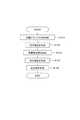
図6は、第1の実施形態に係る表示装置の製造方法を例示するフローチャートである。 図6に表したように、表示装置110の製造方法は、薄膜トランジスタ12を形成するステップS110と、画素電極16を形成するステップS120と、有機発光層18を形成するステップS130と、対向電極20を形成するステップS140と、封止部22を形成するステップS150と、を備える。 FIG. 6 is a flowchart illustrating the method for manufacturing the display device according to the first embodiment. As shown in FIG. 6, the manufacturing method of the
ステップS110では、例えば、図5(a)に関して説明した処理を実施する。ステップS120では、例えば、図5(b)に関して説明した処理を実施する。ステップS130では、例えば、図5(c)に関して説明した処理を実施する。ステップS140では、例えば、図5(d)に関して説明した処理を実施する。ステップS150では、例えば、図5(e)及び図5(f)に関して説明した処理を実施する。 In step S110, for example, the processing described with reference to FIG. In step S120, for example, the processing described with reference to FIG. In step S130, for example, the processing described with reference to FIG. In step S140, for example, the processing described with reference to FIG. In step S150, for example, the processing described with reference to FIGS. 5E and 5F is performed.
図7は、第1の実施形態に係る別の表示装置の構成を例示する模式的断面図である。
図7に表したように、表示装置112の封止部22は、複数の第1封止膜51と複数の第2封止膜52とを交互に積層させた積層膜54を含む。
封止部22に積層膜54を含む表示装置112においても、第1封止膜51及び第2封止膜52の水素の濃度を1020atoms/cm3以下とすることで、薄膜トランジスタ12の閾値電圧の変動が抑制され、表示装置112の画質を高めることができる。FIG. 7 is a schematic cross-sectional view illustrating the configuration of another display device according to the first embodiment.
As illustrated in FIG. 7, the sealing
Also in the
封止部22として、積層膜54を用いることで、封止部22の有機発光層18に対するバリア性を高めることができる。積層膜54では、第1封止膜51に含まれる圧縮応力と、第2封止膜52に含まれる引張応力と、のバランスがより均一になる。これにより、封止部22に含まれる応力の有機発光層18への悪影響を、より適切に抑えることができる。 By using the
(第2実施形態)
図8は、第2の実施形態に係る表示装置の構成を例示する模式的模式図である。
図8に表したように、表示装置210は、対向電極20と封止部22との間に、有機バリア層46を備える。有機バリア層46は、例えば、少なくともポリパラキシレンを含む有機膜である。表示装置210の構成は、有機バリア層46の有無を除いて、表示装置110の構成と同様である。(Second Embodiment)
FIG. 8 is a schematic schematic view illustrating the configuration of a display device according to the second embodiment.
As illustrated in FIG. 8, the
有機バリア層46は、例えば、無機膜である第1封止膜51及び第2封止膜52を成膜するときに使用する酸素プラズマから有機発光層18を保護する。これにより、有機発光層18に加わるダメージを軽減することができる。また、有機バリア層46を形成することにより、封止部22において、コンフォーマルな膜を形成することが可能となる。例えば、有機バリア層46は、ピンホールなどの欠陥を埋める。これにより、封止部22及び有機バリア層46によるバリア性能を向上させることができる。また、有機バリア層46のカバレッジは、第1封止膜51及び第2封止膜52よりも高くすることができる。これにより、より高いバリア性能を得ることができる。 The
図9(a)及び図9(b)は、第2の実施形態に係る表示装置の特性を例示するグラフ図である。
図9(a)及び図9(b)の横軸は、ゲート電圧Vgであり、縦軸は、電流Idである。図9(a)及び図9(b)は、封止部22及び有機バリア層46を形成する前、及び、後の電圧−電流特性をそれぞれ表す。FIG. 9A and FIG. 9B are graphs illustrating characteristics of the display device according to the second embodiment.
9A and 9B, the horizontal axis represents the gate voltage Vg, and the vertical axis represents the current Id. FIGS. 9A and 9B show voltage-current characteristics before and after the sealing
図9(a)及び図9(b)に表したように、本実施形態に係る表示装置210においては、封止部22及び有機バリア層46の形成後において、薄膜トランジスタ12の閾値電圧に変動は見られない。このように、有機バリア層46を設けた表示装置210においても、薄膜トランジスタ12の閾値電圧の変動を抑え、画質を向上させることができる。 As shown in FIGS. 9A and 9B, in the
図10(a)〜図10(c)は、第2の実施形態に係る表示装置の製造方法を例示する模式的断面図である。
表示装置210の製造方法において、対向電極20を形成するまでの手順は、表示装置110の手順と実質的に同じであるから、説明を省略する。
図10(a)に表したように、対向電極20の上に、有機バリア層46を形成する。有機バリア層46は、例えば、熱CVD法によって形成する。FIG. 10A to FIG. 10C are schematic cross-sectional views illustrating the method for manufacturing the display device according to the second embodiment.
In the manufacturing method of the
As shown in FIG. 10A, the
図10(b)に表したように、有機バリア層46の上に、第1封止膜51を形成する。第1封止膜51は、表示装置110において説明したように、スパッタリング法で形成する。第1封止膜51の成膜時のガス圧は、例えば約0.5Pa(例えば0.1Pa以上2.0Pa未満)とする。 As shown in FIG. 10B, the
図10(c)に表したように、第1封止膜51の上に、第2封止膜52を形成する。第2封止膜52は、表示装置110において説明したように、スパッタリング法で形成する。第2封止膜52の成膜時のガス圧は、約3.0Pa(例えば2.0Pa以上10.0Pa未満)とする。これにより、有機バリア層46の上に封止部22が形成される。以上により、表示装置210が完成する。 As shown in FIG. 10C, the
上記実施形態では、下面発光型の表示装置について説明したが、実施形態において、表示装置は、上面発光型でもよい。 Although the bottom emission type display device has been described in the above embodiment, the display device may be a top emission type in the embodiment.
実施形態によれば、高画質の表示装置の製造方法が提供される。 According to the embodiment, a method for manufacturing a high-quality display device is provided.
以上、具体例を参照しつつ、本発明の実施の形態について説明した。
しかし、本発明の実施形態は、これらの具体例に限定されるものではない。例えば、表示装置に含まれる、基板、薄膜トランジスタ、画素電極、有機発光層、対向電極、封止部、第1封止膜、第2封止膜、有機バリア層及び積層膜などの各要素の具体的な構成に関しては、当業者が公知の範囲から適宜選択することにより本発明を同様に実施し、同様の効果を得ることができる限り、本発明の範囲に包含される。
また、各具体例のいずれか2つ以上の要素を技術的に可能な範囲で組み合わせたものも、本発明の要旨を包含する限り本発明の範囲に含まれる。The embodiments of the present invention have been described above with reference to specific examples.
However, embodiments of the present invention are not limited to these specific examples. For example, specific elements included in the display device, such as a substrate, a thin film transistor, a pixel electrode, an organic light emitting layer, a counter electrode, a sealing portion, a first sealing film, a second sealing film, an organic barrier layer, and a laminated film With respect to specific configurations, those skilled in the art can appropriately select from known ranges to implement the present invention in the same manner, and are included in the scope of the present invention as long as similar effects can be obtained.
Moreover, what combined any two or more elements of each specific example in the technically possible range is also included in the scope of the present invention as long as the gist of the present invention is included.
その他、本発明の実施の形態として上述した表示装置の製造方法を基にして、当業者が適宜設計変更して実施し得る全ての表示装置の製造方法も、本発明の要旨を包含する限り、本発明の範囲に属する。 In addition, based on the display device manufacturing method described above as an embodiment of the present invention, all display device manufacturing methods that can be implemented by a person skilled in the art as appropriate are included in the gist of the present invention. It belongs to the scope of the present invention.
その他、本発明の思想の範疇において、当業者であれば、各種の変更例及び修正例に想到し得るものであり、それら変更例及び修正例についても本発明の範囲に属するものと了解される。 In addition, in the category of the idea of the present invention, those skilled in the art can conceive of various changes and modifications, and it is understood that these changes and modifications also belong to the scope of the present invention. .
本発明のいくつかの実施形態を説明したが、これらの実施形態は、例として提示したものであり、発明の範囲を限定することは意図していない。これら新規な実施形態は、その他の様々な形態で実施されることが可能であり、発明の要旨を逸脱しない範囲で、種々の省略、置き換え、変更を行うことができる。これら実施形態やその変形は、発明の範囲や要旨に含まれるとともに、特許請求の範囲に記載された発明とその均等の範囲に含まれる。 Although several embodiments of the present invention have been described, these embodiments are presented by way of example and are not intended to limit the scope of the invention. These novel embodiments can be implemented in various other forms, and various omissions, replacements, and changes can be made without departing from the scope of the invention. These embodiments and modifications thereof are included in the scope and gist of the invention, and are included in the invention described in the claims and the equivalents thereof.
4…本体部、 5…バリア層、 10…基板、 10a…主面、 12…薄膜トランジスタ、 16…画素電極、 16a…対向領域、 16b…非対向領域、 16c…一部、 18…有機発光層、 20…対向電極、 20a…部分、 22…封止部、 24…発光素子部、 31…第1導電部、 32…第2導電部、 33…ゲート電極、 33a…部分、 34…ゲート絶縁膜、 35…半導体膜、 35a…第1領域、 35b…第2領域、 35c…第3領域、 35p…膜面、 36…チャネル保護膜、 36a…第1部分、 36b…第2部分、 40…パッシベーション膜、 40a…開口、 42…平坦化膜、 42a…開口、 44…カラーフィルタ、 44a…開口、 46…有機バリア層、 51…第1封止膜、 52…第2封止膜、 54…積層膜、 110、112、210…表示装置、 Id…電流、 Vg…ゲート電圧、 Vs…変動量 DESCRIPTION OF
Claims (6)
Translated fromJapanese前記第1導電部及び前記第2導電部のいずれか一方に電気的に接続された画素電極を形成する工程と、
前記画素電極の上に有機発光層を形成する工程と、
前記有機発光層の上に対向電極を形成する工程と、
水素の濃度が1020atoms/cm3以下であり圧縮応力及び引張応力のいずれか一方を有する第1封止膜と、前記第1封止膜に積層され水素の濃度が1020atoms/cm3以下であり、圧縮応力と引張応力のいずれか他方を有する第2封止膜と、を含み、前記対向電極を覆う封止部を形成する工程と、
を備えた表示装置の製造方法。A gate electrode is formed on the main surface of the substrate, a gate insulating film is formed on the gate electrode, a semiconductor film is formed on the gate insulating film, and a first electrode electrically connected to the semiconductor film is formed. Forming a first conductive portion and a second conductive portion electrically connected to the semiconductor film, the gate electrode, the gate insulating film, the semiconductor film, the first conductive portion, and the second conductive portion; A step of forming a thin film transistor in which the gate electrode has a portion between the first conductive portion and the second conductive portion when viewed in a direction perpendicular to the film surface of the semiconductor film;
Forming a pixel electrode electrically connected to one of the first conductive portion and the second conductive portion;
Forming an organic light emitting layer on the pixel electrode;
Forming a counter electrode on the organic light emitting layer;
A first sealing film having a hydrogen concentration of 1020 atoms / cm3 or less and having either a compressive stress or a tensile stress, and a hydrogen concentration stacked on the first sealing film is 1020 atoms / cm3. A step of forming a sealing portion that covers the counter electrode, including a second sealing film having one of compressive stress and tensile stress, and
A method for manufacturing a display device comprising:
前記対向電極と前記封止部との間に、少なくともポリパラキシレンを含む有機バリア層を形成することをさらに含む請求項1または2記載の表示装置の製造方法。The step of forming the sealing portion includes
The method of manufacturing a display device according to claim 1, further comprising forming an organic barrier layer containing at least polyparaxylene between the counter electrode and the sealing portion.
Priority Applications (1)
| Application Number | Priority Date | Filing Date | Title |
|---|---|---|---|
| JP2012014237AJP5687638B2 (en) | 2012-01-26 | 2012-01-26 | Manufacturing method of display device |
Applications Claiming Priority (1)
| Application Number | Priority Date | Filing Date | Title |
|---|---|---|---|
| JP2012014237AJP5687638B2 (en) | 2012-01-26 | 2012-01-26 | Manufacturing method of display device |
Publications (2)
| Publication Number | Publication Date |
|---|---|
| JP2013156281Atrue JP2013156281A (en) | 2013-08-15 |
| JP5687638B2 JP5687638B2 (en) | 2015-03-18 |
Family
ID=49051561
Family Applications (1)
| Application Number | Title | Priority Date | Filing Date |
|---|---|---|---|
| JP2012014237AExpired - Fee RelatedJP5687638B2 (en) | 2012-01-26 | 2012-01-26 | Manufacturing method of display device |
Country Status (1)
| Country | Link |
|---|---|
| JP (1) | JP5687638B2 (en) |
Cited By (6)
| Publication number | Priority date | Publication date | Assignee | Title |
|---|---|---|---|---|
| US20130313547A1 (en)* | 2012-05-22 | 2013-11-28 | Shintaro Nakano | Display device |
| US20150243924A1 (en)* | 2012-02-08 | 2015-08-27 | Joled Inc. | Method of manufacturing organic el element and organic el element |
| JP2015179248A (en)* | 2013-10-25 | 2015-10-08 | 株式会社半導体エネルギー研究所 | display device |
| US9960385B2 (en) | 2015-10-14 | 2018-05-01 | Japan Display Inc. | Organic EL display device |
| WO2018193340A1 (en)* | 2017-04-20 | 2018-10-25 | 株式会社半導体エネルギー研究所 | Display panel, display device, input-output device, and information processing device |
| US11502110B2 (en) | 2020-03-18 | 2022-11-15 | Samsung Display Co., Ltd. | Display device and method of manufacturing the same |
Citations (9)
| Publication number | Priority date | Publication date | Assignee | Title |
|---|---|---|---|---|
| JP2001284042A (en)* | 2000-03-31 | 2001-10-12 | Denso Corp | Organic EL device |
| JP2004047409A (en)* | 2001-10-30 | 2004-02-12 | Semiconductor Energy Lab Co Ltd | Light emitting device |
| JP2004079509A (en)* | 2002-05-17 | 2004-03-11 | Semiconductor Energy Lab Co Ltd | Display device |
| JP2005222778A (en)* | 2004-02-04 | 2005-08-18 | Shimadzu Corp | Organic electroluminescence device and method for producing the same |
| JP2006004917A (en)* | 2004-05-20 | 2006-01-05 | Semiconductor Energy Lab Co Ltd | Light-emitting element and display device |
| JP2006024421A (en)* | 2004-07-07 | 2006-01-26 | Seiko Epson Corp | Electro-optical device, method of manufacturing electro-optical device, and electronic apparatus |
| JP2008004362A (en)* | 2006-06-22 | 2008-01-10 | Casio Comput Co Ltd | Display device and manufacturing method thereof |
| JP2008141119A (en)* | 2006-12-05 | 2008-06-19 | Canon Inc | Display device using oxide semiconductor and manufacturing method thereof |
| JP2010262057A (en)* | 2009-04-30 | 2010-11-18 | Sharp Corp | Display device and information card provided with the same |
- 2012
- 2012-01-26JPJP2012014237Apatent/JP5687638B2/ennot_activeExpired - Fee Related
Patent Citations (9)
| Publication number | Priority date | Publication date | Assignee | Title |
|---|---|---|---|---|
| JP2001284042A (en)* | 2000-03-31 | 2001-10-12 | Denso Corp | Organic EL device |
| JP2004047409A (en)* | 2001-10-30 | 2004-02-12 | Semiconductor Energy Lab Co Ltd | Light emitting device |
| JP2004079509A (en)* | 2002-05-17 | 2004-03-11 | Semiconductor Energy Lab Co Ltd | Display device |
| JP2005222778A (en)* | 2004-02-04 | 2005-08-18 | Shimadzu Corp | Organic electroluminescence device and method for producing the same |
| JP2006004917A (en)* | 2004-05-20 | 2006-01-05 | Semiconductor Energy Lab Co Ltd | Light-emitting element and display device |
| JP2006024421A (en)* | 2004-07-07 | 2006-01-26 | Seiko Epson Corp | Electro-optical device, method of manufacturing electro-optical device, and electronic apparatus |
| JP2008004362A (en)* | 2006-06-22 | 2008-01-10 | Casio Comput Co Ltd | Display device and manufacturing method thereof |
| JP2008141119A (en)* | 2006-12-05 | 2008-06-19 | Canon Inc | Display device using oxide semiconductor and manufacturing method thereof |
| JP2010262057A (en)* | 2009-04-30 | 2010-11-18 | Sharp Corp | Display device and information card provided with the same |
Cited By (12)
| Publication number | Priority date | Publication date | Assignee | Title |
|---|---|---|---|---|
| US20150243924A1 (en)* | 2012-02-08 | 2015-08-27 | Joled Inc. | Method of manufacturing organic el element and organic el element |
| US9196861B2 (en)* | 2012-02-08 | 2015-11-24 | Joled Inc. | Method of manufacturing organic EL element and organic EL element |
| US20130313547A1 (en)* | 2012-05-22 | 2013-11-28 | Shintaro Nakano | Display device |
| US8916858B2 (en)* | 2012-05-22 | 2014-12-23 | Kabushiki Kaisha Toshiba | Display device |
| JP2015179248A (en)* | 2013-10-25 | 2015-10-08 | 株式会社半導体エネルギー研究所 | display device |
| US10269888B2 (en) | 2013-10-25 | 2019-04-23 | Semiconductor Energy Laboratory Co., Ltd. | Display device |
| US9960385B2 (en) | 2015-10-14 | 2018-05-01 | Japan Display Inc. | Organic EL display device |
| WO2018193340A1 (en)* | 2017-04-20 | 2018-10-25 | 株式会社半導体エネルギー研究所 | Display panel, display device, input-output device, and information processing device |
| JPWO2018193340A1 (en)* | 2017-04-20 | 2020-03-26 | 株式会社半導体エネルギー研究所 | Display panel, display device, input / output device, information processing device |
| JP7114574B2 (en) | 2017-04-20 | 2022-08-08 | 株式会社半導体エネルギー研究所 | display panel |
| US11502110B2 (en) | 2020-03-18 | 2022-11-15 | Samsung Display Co., Ltd. | Display device and method of manufacturing the same |
| US12027527B2 (en) | 2020-03-18 | 2024-07-02 | Samsung Display Co., Ltd. | Display device and method of manufacturing the same |
Also Published As
| Publication number | Publication date |
|---|---|
| JP5687638B2 (en) | 2015-03-18 |
Similar Documents
| Publication | Publication Date | Title |
|---|---|---|
| JP5674707B2 (en) | Display device | |
| JP5636392B2 (en) | Display device | |
| US8841666B2 (en) | Display device | |
| JP6262276B2 (en) | Oxide thin film transistor and method for manufacturing the same | |
| JP5685558B2 (en) | Display device | |
| JP5687638B2 (en) | Manufacturing method of display device | |
| US10804404B2 (en) | Thin film transistor array panel and manufacturing method thereof | |
| WO2015029286A1 (en) | Thin film transistor substrate manufacturing method and thin film transistor substrate | |
| CN111081734B (en) | Thin film transistor element substrate and manufacturing method thereof, and organic EL display device | |
| KR20220001506A (en) | Thin Film Transistor Substrate Having Bi-Layer Oxide Semiconductor | |
| JP5779161B2 (en) | Thin film transistor and display device | |
| TW201334176A (en) | Organic light emitting diode display | |
| KR102434908B1 (en) | Thin film trnasistor comprising oxide semiconductor layer, method for manufacturing the same and display device comprising the same | |
| KR102453920B1 (en) | Organic light emitting display apparatus and the manufacturing method thereof | |
| JP5693479B2 (en) | Manufacturing method of display device | |
| WO2015186349A1 (en) | Thin film transistor substrate manufacturing method | |
| JP2015065202A (en) | Semiconductor element, display device, method of manufacturing semiconductor element, and method of manufacturing display device |
Legal Events
| Date | Code | Title | Description |
|---|---|---|---|
| A621 | Written request for application examination | Free format text:JAPANESE INTERMEDIATE CODE: A621 Effective date:20140203 | |
| A131 | Notification of reasons for refusal | Free format text:JAPANESE INTERMEDIATE CODE: A131 Effective date:20140811 | |
| A977 | Report on retrieval | Free format text:JAPANESE INTERMEDIATE CODE: A971007 Effective date:20140813 | |
| A521 | Request for written amendment filed | Free format text:JAPANESE INTERMEDIATE CODE: A523 Effective date:20141002 | |
| TRDD | Decision of grant or rejection written | ||
| A01 | Written decision to grant a patent or to grant a registration (utility model) | Free format text:JAPANESE INTERMEDIATE CODE: A01 Effective date:20141226 | |
| A61 | First payment of annual fees (during grant procedure) | Free format text:JAPANESE INTERMEDIATE CODE: A61 Effective date:20150122 | |
| LAPS | Cancellation because of no payment of annual fees |