JP2013145174A - Proximity sensor - Google Patents
Proximity sensorDownload PDFInfo
- Publication number
- JP2013145174A JP2013145174AJP2012005554AJP2012005554AJP2013145174AJP 2013145174 AJP2013145174 AJP 2013145174AJP 2012005554 AJP2012005554 AJP 2012005554AJP 2012005554 AJP2012005554 AJP 2012005554AJP 2013145174 AJP2013145174 AJP 2013145174A
- Authority
- JP
- Japan
- Prior art keywords
- light
- light emitting
- proximity sensor
- light receiving
- detected
- Prior art date
- Legal status (The legal status is an assumption and is not a legal conclusion. Google has not performed a legal analysis and makes no representation as to the accuracy of the status listed.)
- Pending
Links
Images


Classifications
- G—PHYSICS
- G01—MEASURING; TESTING
- G01V—GEOPHYSICS; GRAVITATIONAL MEASUREMENTS; DETECTING MASSES OR OBJECTS; TAGS
- G01V8/00—Prospecting or detecting by optical means
- G01V8/10—Detecting, e.g. by using light barriers
- G01V8/20—Detecting, e.g. by using light barriers using multiple transmitters or receivers
- G—PHYSICS
- G01—MEASURING; TESTING
- G01B—MEASURING LENGTH, THICKNESS OR SIMILAR LINEAR DIMENSIONS; MEASURING ANGLES; MEASURING AREAS; MEASURING IRREGULARITIES OF SURFACES OR CONTOURS
- G01B11/00—Measuring arrangements characterised by the use of optical techniques
- G01B11/14—Measuring arrangements characterised by the use of optical techniques for measuring distance or clearance between spaced objects or spaced apertures
- G—PHYSICS
- G01—MEASURING; TESTING
- G01J—MEASUREMENT OF INTENSITY, VELOCITY, SPECTRAL CONTENT, POLARISATION, PHASE OR PULSE CHARACTERISTICS OF INFRARED, VISIBLE OR ULTRAVIOLET LIGHT; COLORIMETRY; RADIATION PYROMETRY
- G01J1/00—Photometry, e.g. photographic exposure meter
- G01J1/42—Photometry, e.g. photographic exposure meter using electric radiation detectors
- G01J1/429—Photometry, e.g. photographic exposure meter using electric radiation detectors applied to measurement of ultraviolet light
- G—PHYSICS
- G01—MEASURING; TESTING
- G01J—MEASUREMENT OF INTENSITY, VELOCITY, SPECTRAL CONTENT, POLARISATION, PHASE OR PULSE CHARACTERISTICS OF INFRARED, VISIBLE OR ULTRAVIOLET LIGHT; COLORIMETRY; RADIATION PYROMETRY
- G01J5/00—Radiation pyrometry, e.g. infrared or optical thermometry
- G01J5/0022—Radiation pyrometry, e.g. infrared or optical thermometry for sensing the radiation of moving bodies
- G01J5/0025—Living bodies
- G—PHYSICS
- G01—MEASURING; TESTING
- G01J—MEASUREMENT OF INTENSITY, VELOCITY, SPECTRAL CONTENT, POLARISATION, PHASE OR PULSE CHARACTERISTICS OF INFRARED, VISIBLE OR ULTRAVIOLET LIGHT; COLORIMETRY; RADIATION PYROMETRY
- G01J5/00—Radiation pyrometry, e.g. infrared or optical thermometry
- G01J5/02—Constructional details
- G01J5/08—Optical arrangements
- G01J5/0808—Convex mirrors
- G—PHYSICS
- G01—MEASURING; TESTING
- G01J—MEASUREMENT OF INTENSITY, VELOCITY, SPECTRAL CONTENT, POLARISATION, PHASE OR PULSE CHARACTERISTICS OF INFRARED, VISIBLE OR ULTRAVIOLET LIGHT; COLORIMETRY; RADIATION PYROMETRY
- G01J5/00—Radiation pyrometry, e.g. infrared or optical thermometry
- G01J5/02—Constructional details
- G01J5/08—Optical arrangements
- G01J5/0868—Means for illuminating a slit or a surface efficiently, e.g. entrance slit of a pyrometer or entrance face of a fiber
- G—PHYSICS
- G01—MEASURING; TESTING
- G01J—MEASUREMENT OF INTENSITY, VELOCITY, SPECTRAL CONTENT, POLARISATION, PHASE OR PULSE CHARACTERISTICS OF INFRARED, VISIBLE OR ULTRAVIOLET LIGHT; COLORIMETRY; RADIATION PYROMETRY
- G01J5/00—Radiation pyrometry, e.g. infrared or optical thermometry
- G01J5/02—Constructional details
- G01J5/08—Optical arrangements
- G01J5/0896—Optical arrangements using a light source, e.g. for illuminating a surface
- G—PHYSICS
- G01—MEASURING; TESTING
- G01S—RADIO DIRECTION-FINDING; RADIO NAVIGATION; DETERMINING DISTANCE OR VELOCITY BY USE OF RADIO WAVES; LOCATING OR PRESENCE-DETECTING BY USE OF THE REFLECTION OR RERADIATION OF RADIO WAVES; ANALOGOUS ARRANGEMENTS USING OTHER WAVES
- G01S17/00—Systems using the reflection or reradiation of electromagnetic waves other than radio waves, e.g. lidar systems
- G01S17/02—Systems using the reflection of electromagnetic waves other than radio waves
- G01S17/04—Systems determining the presence of a target
- G—PHYSICS
- G01—MEASURING; TESTING
- G01S—RADIO DIRECTION-FINDING; RADIO NAVIGATION; DETERMINING DISTANCE OR VELOCITY BY USE OF RADIO WAVES; LOCATING OR PRESENCE-DETECTING BY USE OF THE REFLECTION OR RERADIATION OF RADIO WAVES; ANALOGOUS ARRANGEMENTS USING OTHER WAVES
- G01S7/00—Details of systems according to groups G01S13/00, G01S15/00, G01S17/00
- G01S7/48—Details of systems according to groups G01S13/00, G01S15/00, G01S17/00 of systems according to group G01S17/00
- G01S7/481—Constructional features, e.g. arrangements of optical elements
- G01S7/4811—Constructional features, e.g. arrangements of optical elements common to transmitter and receiver
- G01S7/4813—Housing arrangements
- G—PHYSICS
- G01—MEASURING; TESTING
- G01S—RADIO DIRECTION-FINDING; RADIO NAVIGATION; DETERMINING DISTANCE OR VELOCITY BY USE OF RADIO WAVES; LOCATING OR PRESENCE-DETECTING BY USE OF THE REFLECTION OR RERADIATION OF RADIO WAVES; ANALOGOUS ARRANGEMENTS USING OTHER WAVES
- G01S7/00—Details of systems according to groups G01S13/00, G01S15/00, G01S17/00
- G01S7/48—Details of systems according to groups G01S13/00, G01S15/00, G01S17/00 of systems according to group G01S17/00
- G01S7/481—Constructional features, e.g. arrangements of optical elements
- G01S7/4814—Constructional features, e.g. arrangements of optical elements of transmitters alone
- G01S7/4815—Constructional features, e.g. arrangements of optical elements of transmitters alone using multiple transmitters
- G—PHYSICS
- G06—COMPUTING OR CALCULATING; COUNTING
- G06F—ELECTRIC DIGITAL DATA PROCESSING
- G06F3/00—Input arrangements for transferring data to be processed into a form capable of being handled by the computer; Output arrangements for transferring data from processing unit to output unit, e.g. interface arrangements
- G06F3/01—Input arrangements or combined input and output arrangements for interaction between user and computer
- G06F3/03—Arrangements for converting the position or the displacement of a member into a coded form
- G06F3/0304—Detection arrangements using opto-electronic means
- G—PHYSICS
- G06—COMPUTING OR CALCULATING; COUNTING
- G06F—ELECTRIC DIGITAL DATA PROCESSING
- G06F3/00—Input arrangements for transferring data to be processed into a form capable of being handled by the computer; Output arrangements for transferring data from processing unit to output unit, e.g. interface arrangements
- G06F3/01—Input arrangements or combined input and output arrangements for interaction between user and computer
- G06F3/03—Arrangements for converting the position or the displacement of a member into a coded form
- G06F3/033—Pointing devices displaced or positioned by the user, e.g. mice, trackballs, pens or joysticks; Accessories therefor
- G06F3/0354—Pointing devices displaced or positioned by the user, e.g. mice, trackballs, pens or joysticks; Accessories therefor with detection of 2D relative movements between the device, or an operating part thereof, and a plane or surface, e.g. 2D mice, trackballs, pens or pucks
- G06F3/03547—Touch pads, in which fingers can move on a surface
- H—ELECTRICITY
- H03—ELECTRONIC CIRCUITRY
- H03K—PULSE TECHNIQUE
- H03K17/00—Electronic switching or gating, i.e. not by contact-making and –breaking
- H03K17/94—Electronic switching or gating, i.e. not by contact-making and –breaking characterised by the way in which the control signals are generated
- H03K17/941—Electronic switching or gating, i.e. not by contact-making and –breaking characterised by the way in which the control signals are generated using an optical detector
- H03K17/943—Electronic switching or gating, i.e. not by contact-making and –breaking characterised by the way in which the control signals are generated using an optical detector using a plurality of optical emitters or detectors, e.g. keyboard
- H—ELECTRICITY
- H05—ELECTRIC TECHNIQUES NOT OTHERWISE PROVIDED FOR
- H05K—PRINTED CIRCUITS; CASINGS OR CONSTRUCTIONAL DETAILS OF ELECTRIC APPARATUS; MANUFACTURE OF ASSEMBLAGES OF ELECTRICAL COMPONENTS
- H05K1/00—Printed circuits
- H05K1/02—Details
- H05K1/0284—Details of three-dimensional rigid printed circuit boards
- H—ELECTRICITY
- H01—ELECTRIC ELEMENTS
- H01L—SEMICONDUCTOR DEVICES NOT COVERED BY CLASS H10
- H01L2924/00—Indexing scheme for arrangements or methods for connecting or disconnecting semiconductor or solid-state bodies as covered by H01L24/00
- H01L2924/15—Details of package parts other than the semiconductor or other solid state devices to be connected
- H01L2924/151—Die mounting substrate
- H01L2924/1515—Shape
- H01L2924/15153—Shape the die mounting substrate comprising a recess for hosting the device
- H01L2924/15155—Shape the die mounting substrate comprising a recess for hosting the device the shape of the recess being other than a cuboid
- H01L2924/15156—Side view
- H—ELECTRICITY
- H03—ELECTRONIC CIRCUITRY
- H03K—PULSE TECHNIQUE
- H03K17/00—Electronic switching or gating, i.e. not by contact-making and –breaking
- H03K17/94—Electronic switching or gating, i.e. not by contact-making and –breaking characterised by the way in which the control signals are generated
- H03K17/945—Proximity switches
- H03K2017/9455—Proximity switches constructional details
- H—ELECTRICITY
- H03—ELECTRONIC CIRCUITRY
- H03K—PULSE TECHNIQUE
- H03K2217/00—Indexing scheme related to electronic switching or gating, i.e. not by contact-making or -breaking covered by H03K17/00
- H03K2217/94—Indexing scheme related to electronic switching or gating, i.e. not by contact-making or -breaking covered by H03K17/00 characterised by the way in which the control signal is generated
- H03K2217/941—Indexing scheme related to electronic switching or gating, i.e. not by contact-making or -breaking covered by H03K17/00 characterised by the way in which the control signal is generated using an optical detector
- H03K2217/94111—Indexing scheme related to electronic switching or gating, i.e. not by contact-making or -breaking covered by H03K17/00 characterised by the way in which the control signal is generated using an optical detector having more than one emitter
- H—ELECTRICITY
- H05—ELECTRIC TECHNIQUES NOT OTHERWISE PROVIDED FOR
- H05K—PRINTED CIRCUITS; CASINGS OR CONSTRUCTIONAL DETAILS OF ELECTRIC APPARATUS; MANUFACTURE OF ASSEMBLAGES OF ELECTRICAL COMPONENTS
- H05K2201/00—Indexing scheme relating to printed circuits covered by H05K1/00
- H05K2201/03—Conductive materials
- H05K2201/0332—Structure of the conductor
- H05K2201/0335—Layered conductors or foils
- H05K2201/0338—Layered conductor, e.g. layered metal substrate, layered finish layer or layered thin film adhesion layer
- H—ELECTRICITY
- H05—ELECTRIC TECHNIQUES NOT OTHERWISE PROVIDED FOR
- H05K—PRINTED CIRCUITS; CASINGS OR CONSTRUCTIONAL DETAILS OF ELECTRIC APPARATUS; MANUFACTURE OF ASSEMBLAGES OF ELECTRICAL COMPONENTS
- H05K2201/00—Indexing scheme relating to printed circuits covered by H05K1/00
- H05K2201/10—Details of components or other objects attached to or integrated in a printed circuit board
- H05K2201/10007—Types of components
- H05K2201/10151—Sensor
- H—ELECTRICITY
- H05—ELECTRIC TECHNIQUES NOT OTHERWISE PROVIDED FOR
- H05K—PRINTED CIRCUITS; CASINGS OR CONSTRUCTIONAL DETAILS OF ELECTRIC APPARATUS; MANUFACTURE OF ASSEMBLAGES OF ELECTRICAL COMPONENTS
- H05K2201/00—Indexing scheme relating to printed circuits covered by H05K1/00
- H05K2201/20—Details of printed circuits not provided for in H05K2201/01 - H05K2201/10
- H05K2201/2054—Light-reflecting surface, e.g. conductors, substrates, coatings, dielectrics
- H—ELECTRICITY
- H05—ELECTRIC TECHNIQUES NOT OTHERWISE PROVIDED FOR
- H05K—PRINTED CIRCUITS; CASINGS OR CONSTRUCTIONAL DETAILS OF ELECTRIC APPARATUS; MANUFACTURE OF ASSEMBLAGES OF ELECTRICAL COMPONENTS
- H05K3/00—Apparatus or processes for manufacturing printed circuits
- H05K3/10—Apparatus or processes for manufacturing printed circuits in which conductive material is applied to the insulating support in such a manner as to form the desired conductive pattern
- H05K3/108—Apparatus or processes for manufacturing printed circuits in which conductive material is applied to the insulating support in such a manner as to form the desired conductive pattern by semi-additive methods; masks therefor
Landscapes
- Engineering & Computer Science (AREA)
- Physics & Mathematics (AREA)
- General Physics & Mathematics (AREA)
- Spectroscopy & Molecular Physics (AREA)
- General Engineering & Computer Science (AREA)
- Theoretical Computer Science (AREA)
- Remote Sensing (AREA)
- Radar, Positioning & Navigation (AREA)
- Computer Networks & Wireless Communication (AREA)
- Electromagnetism (AREA)
- Human Computer Interaction (AREA)
- Life Sciences & Earth Sciences (AREA)
- Geophysics (AREA)
- General Life Sciences & Earth Sciences (AREA)
- Microelectronics & Electronic Packaging (AREA)
- Switches Operated By Changes In Physical Conditions (AREA)
- Length Measuring Devices By Optical Means (AREA)
- Geophysics And Detection Of Objects (AREA)
- Measurement Of Optical Distance (AREA)
- Photometry And Measurement Of Optical Pulse Characteristics (AREA)
- Manufacturing Of Printed Circuit Boards (AREA)
Abstract
Translated fromJapaneseDescription
Translated fromJapanese本発明は、被検出物を検出する近接センサに関する。 The present invention relates to a proximity sensor that detects an object to be detected.
近年、携帯情報端末等の電子機器は、機能毎に製造された各モジュールが基板上に組み合わせて実装されることが多く、電子機器の高機能化が急速に進展している。また、省資源化及び携帯性の観点から、電子機器の薄型化及び軽量化が望まれている。 2. Description of the Related Art In recent years, electronic devices such as portable information terminals are often mounted with a combination of modules manufactured for each function on a substrate. In addition, from the viewpoint of resource saving and portability, it is desired to make electronic devices thinner and lighter.
しかし、電子回路を形成するガラスエポキシ基板等のプリント配線基板は平面的な構造をしており、更に電子部品の実装形態にも制約があるため、更なる高機能化と薄型化と軽量化とを同時に達成することが困難となっている。 However, printed wiring boards such as glass epoxy boards that form electronic circuits have a planar structure, and there are also restrictions on the mounting form of electronic components. Is difficult to achieve at the same time.
この様な背景の下、射出成形品の表面に立体的な電気回路を直接的に形成するMID(Molded Interconnected Device)技術が脚光を浴びている。MID技術は、モジュールを実装するためのモジュール基板に、機構部品としての機械的機能と配線回路基板としての電気的機能とを与えることができる。従って、MID技術によれば、電子機器の小型化と電子機器を構成するモジュール基板の高精度化とを同時に実現することができ、更に、モジュール基板の組み立て工数を削減することもできる。 Under such a background, MID (Molded Interconnected Device) technology that directly forms a three-dimensional electric circuit on the surface of an injection-molded product is in the spotlight. The MID technique can give a mechanical function as a mechanical component and an electrical function as a printed circuit board to a module board for mounting the module. Therefore, according to the MID technology, it is possible to simultaneously reduce the size of the electronic device and increase the accuracy of the module substrate that constitutes the electronic device, and it is also possible to reduce the man-hours for assembling the module substrate.
また、携帯端末又はタブレット端末等の電子機器では、近接センサの一例として、タッチレスモーション機能を搭載することが検討されている。タッチレスモーション機能は、携帯端末又はタブレット端末等の電子機器のディスプレイにユーザの手がタッチされずに、ユーザの手が当該ディスプレイ上において例えば上下方向又は左右方向に動いたことを検出する機能である。 In addition, in an electronic device such as a portable terminal or a tablet terminal, it is considered to install a touchless motion function as an example of a proximity sensor. The touchless motion function is a function for detecting that the user's hand has moved, for example, up and down or left and right on the display without touching the display of an electronic device such as a mobile terminal or a tablet terminal. is there.
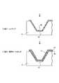
これまでに、発光部としての3つのLED素子を駆動し、タッチレスモーション機能を実現するドライバを搭載した受光素子が提供されている。図12(A)は、従来のタッチレスモーション機能におけるユーザの手の左右方向の動きの検出動作を説明する図である。図12(B)は、従来のタッチレスモーション機能におけるユーザの手の上下方向の動きの検出動作を説明する図である。図12(C)は、ユーザの手の左右方向の動きに対する反射光の信号強度を説明する図である。図12(D)は、ユーザの手の上下方向の動きに対する反射光の信号強度を説明する図である。図12(E)は、各IrLED101、102、103の発光タイミングを説明する図である。 So far, a light receiving element equipped with a driver that drives three LED elements as a light emitting unit and realizes a touchless motion function has been provided. FIG. 12A is a diagram for explaining a motion detection operation in the horizontal direction of the user's hand in the conventional touchless motion function. FIG. 12B is a diagram for explaining an operation of detecting the vertical movement of the user's hand in the conventional touchless motion function. FIG. 12C is a diagram illustrating the signal intensity of the reflected light with respect to the movement of the user's hand in the left-right direction. FIG. 12D is a diagram illustrating the signal intensity of reflected light with respect to the vertical movement of the user's hand. FIG. 12E is a diagram illustrating the light emission timing of each of the IrLEDs 101, 102, and 103.
図12(A)に示す様に、携帯端末100の上部であって携帯端末100の筺体内部には、図12(A)の紙面の横方向及び縦方向に対して90°の角度をなす様に、3つの近赤外発光素子(IrLED)101、102、103が配置されている。また、図12(A)に示す様に、携帯端末100の上部であって携帯端末100の筺体内部には、横方向の2つのIrLED101、102の間には、受光素子105が配置されている。 As shown in FIG. 12A, the top of the
3つのIrLED101、102、103は、図12(E)に示す様に、周期10ms〜2000msの発光周期で可変自在な発光タイミングで時分割に発光する。図12(A)及び図12(C)に示す様に、携帯端末100に対し、ユーザの手106を右から左に移動させると、受光素子105は、右側に位置する2つのIrLED102、103から時分割に発光された光の反射光を受光する。さらに、受光素子105は、少し遅れて、左側に位置する1つのIrLED101からの反射光を受光する。この受光するタイミングのずれにより、ユーザの手106の左右方向のモーションが検出される。 As shown in FIG. 12E, the three IrLEDs 101, 102, and 103 emit light in a time-sharing manner with a variable light emission timing with a light emission period of 10 ms to 2000 ms. As shown in FIGS. 12A and 12C, when the user's
同様に、図12(C)及び図12(D)に示す様に、携帯端末100に対し、ユーザの手106を上から下に移動させると、受光素子105は、上側に位置する2つのIrLED101、102から時分割に発光された光の反射光を受光する。さらに、受光素子105は、少し遅れて、下側に位置する1つのIrLED103からの反射光を受光する。この受光するタイミングのずれにより、ユーザの手106の上下方向のモーションが検出される。 Similarly, as shown in FIGS. 12C and 12D, when the user's
近接センサに関する先行技術として、基板と、この基板上に列状に配置された複数の受光素子と、各受光素子に対して複数個ずつ対応して設けられ、列状に配置された複数の発光素子とを備えた、受発光一体型素子アレイが知られている(例えば特許文献1参照)。この受発光一体型素子アレイは、列状に設けられた発光素子からの光に対する検出対象物の反射光の大きさ(光電流の大きさ)を基に、検出対象物の位置を検出する。 As prior art related to proximity sensors, a substrate, a plurality of light receiving elements arranged in a row on the substrate, and a plurality of light emitting elements arranged in a row corresponding to each light receiving element A light receiving / emitting integrated element array including elements is known (see, for example, Patent Document 1). The light receiving / emitting integrated element array detects the position of the detection target based on the magnitude of reflected light (the magnitude of the photocurrent) of the detection target with respect to the light from the light emitting elements provided in a row.
しかしながら、上記した従来の近接センサには、次の様な問題があった。従来、携帯端末又はタブレット端末等の電子機器にタッチレスモーション機能を搭載する場合、それぞれの発光部としての例えばIrLEDを個別に基板に配置しなければならなかった。このため、電子機器を組み立てるセットメーカは、基板を設計する際、各発光部と受光部の位置関係を決め、この位置関係に適した発光部の発光タイミング(発光周期)の調整を行わなければならず、面倒な設計を行う必要があった。 However, the conventional proximity sensor described above has the following problems. Conventionally, when a touchless motion function is mounted on an electronic device such as a portable terminal or a tablet terminal, for example, IrLEDs as respective light emitting units have to be individually arranged on a substrate. For this reason, a set manufacturer that assembles an electronic device must determine the positional relationship between each light emitting unit and the light receiving unit when designing a board, and do not adjust the light emission timing (light emission cycle) of the light emitting unit suitable for this positional relationship. Rather, it was necessary to perform a troublesome design.
また、特許文献1に記載の受発光一体型素子アレイは、所定の方向(例えば横方向)における検出対象物の位置を検出するが、他の方向(例えば縦方向)を含めて検出することを行っていなかった。 In addition, the light receiving and emitting integrated element array described in
本発明は、従来の事情に鑑みてなされたものであり、あらかじめ発光部の発光タイミングを調整して基板の設計を簡単にし、被検出物を高精度に検出することができる近接センサを提供することを目的とする。 The present invention has been made in view of the conventional circumstances, and provides a proximity sensor that can adjust the light emission timing of a light emitting unit in advance to simplify the design of a substrate and detect an object to be detected with high accuracy. For the purpose.
本発明の第1の近接センサは、被検出物を検出する近接センサであって、基板と、全てが直線に並ばない様に、前記基板の面に配置され、光を出射する少なくとも3つの発光部と、前記少なくとも3つの発光部と所定の位置関係となる様に、前記基板の面に配置され、前記発光部から出射され、前記被検出物で反射された光を受光する受光部と、を備える。 The first proximity sensor of the present invention is a proximity sensor that detects an object to be detected, and is arranged on the surface of the substrate so as not to line up with the substrate, and emits light. A light receiving portion that is disposed on the surface of the substrate so as to be in a predetermined positional relationship with the at least three light emitting portions, and that receives the light emitted from the light emitting portion and reflected by the object to be detected; Is provided.
本発明の第2の近接センサは、前記基板は、1ショットレーザ輪郭除去法で製造された立体回路基板であることを特徴とする。 In the second proximity sensor of the present invention, the substrate is a three-dimensional circuit substrate manufactured by a one-shot laser contour removal method.
本発明の第3の近接センサは、前記少なくとも3つの発光部及び前記受光部が、それぞれ前記基板の表面に形成された凹部に実装されることを特徴とする。 The third proximity sensor according to the present invention is characterized in that the at least three light emitting portions and the light receiving portion are each mounted in a recess formed on a surface of the substrate.
本発明の第4の近接センサは、前記受光部が、前記少なくとも3つの発光部から出射されて前記被検出物で反射された反射光の受光パターンを基に、前記被検出物の移動を検出することを特徴とする。 In the fourth proximity sensor of the present invention, the light receiving unit detects movement of the detected object based on a light receiving pattern of reflected light emitted from the at least three light emitting units and reflected by the detected object. It is characterized by doing.
本発明の第5の近接センサは、前記少なくとも3つの発光部から出射される光の発光量が異なり、前記受光部は、前記反射された光の受光量をもとに、前記面に対して垂直方向の前記被検出物の距離を検出することを特徴とする。 In the fifth proximity sensor of the present invention, the light emission amounts of the light emitted from the at least three light emission units are different, and the light reception unit is arranged on the surface based on the light reception amount of the reflected light. The distance of the detected object in the vertical direction is detected.
本発明の第6の近接センサは、前記少なくとも3つの発光部が載置される凹部が、前記受光部に対し、前記発光部から出射される光が外側を向く様に、前記外側に偏った開口部を有することを特徴とする。 In the sixth proximity sensor of the present invention, the concave portion on which the at least three light emitting units are placed is biased toward the outside so that the light emitted from the light emitting unit faces the outside with respect to the light receiving unit. It has an opening.
本発明の第7の近接センサは、前記基板の面に、前記受光部及び3つの前記発光部が矩形の四隅となるように配置されたことを特徴とする。 The seventh proximity sensor of the present invention is characterized in that the light receiving portion and the three light emitting portions are arranged on the surface of the substrate so as to form four corners of a rectangle.
本発明の第8の近接センサは、前記基板の面の中央に前記受光部が配置され、前記受光部の周囲に4つの前記発光部が配置されたことを特徴とする。 The eighth proximity sensor of the present invention is characterized in that the light receiving part is arranged at the center of the surface of the substrate, and four light emitting parts are arranged around the light receiving part.
本発明によれば、あらかじめ発光部の発光タイミングを調整して基板の設計を簡単にし、被検出物を高精度に検出することができる。 According to the present invention, it is possible to adjust the light emission timing of the light emitting unit in advance to simplify the design of the substrate, and to detect an object to be detected with high accuracy.
本発明に係る近接センサの実施形態について、図面を参照して説明する。 An embodiment of a proximity sensor according to the present invention will be described with reference to the drawings.
本実施形態の近接センサは、携帯端末又はタブレット端末等の電子機器の筐体内部に設けられ、ユーザの手又は指等の被検出物を検出するものである。 The proximity sensor of the present embodiment is provided inside a housing of an electronic device such as a mobile terminal or a tablet terminal, and detects an object to be detected such as a user's hand or a finger.
(第1の実施形態)
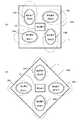
図1は、第1の実施形態の近接センサ19における発光素子及び受光素子の配置を示す図である。近接センサ19は、立体回路基板1の上面に、少なくとも3つの発光素子10A、10B、10Cと1つの受光素子32とが実装されて構成されている。図1に示す様に、立体回路基板1の上面には、3つの発光素子10A、10B、10Cと1つの受光素子32が矩形の四隅に配置されている。即ち、立体回路基板1は、各発光素子10A、10B、10Cの電気回路が実装される例えば円形の底部(底面)と当該底部(底面)の周囲を囲む壁面とにより形成された円形の凹部(不図示)と、受光素子32の電気回路が実装される例えば矩形の底部(底面)と当該底部(底面)の周囲を囲む壁面とにより形成された矩形の凹部(不図示)とを有する構成である。(First embodiment)
FIG. 1 is a diagram illustrating an arrangement of light emitting elements and light receiving elements in the
発光部としての発光素子10A、10B、10Cは、駆動電流が供給されると、(発光1)、(発光2)、(発光3)の順に時分割で赤外線(例えば、近赤外線)を発するIrLEDにより構成される。 When a driving current is supplied, the
受光部としての受光素子32は、フォトダイオードと、フォトダイオードを駆動するためのドライバ回路とを有する構成である。このドライバ回路は、後述する様に、タッチレスモーション機能、及び被検出物までの距離を検出する機能を有する。 The
また、近接センサ19は、MID技術による製造プロセスで製造された立体回路基板1に、発光素子10A、10B、10C及び受光素子32が実装されることによって製造される(図4参照)。 The
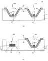
図2は、第1の実施形態における1ショットレーザ輪郭除去法による立体回路基板の製造プロセスの前半部を、立体回路基板の断面図を用いて時系列に説明する図である。図3は、第1の実施形態における1ショットレーザ輪郭除去法による立体回路基板の製造プロセスの後半部を、立体回路基板の断面図を用いて時系列に説明する図である。 FIG. 2 is a diagram for explaining the first half of the manufacturing process of the three-dimensional circuit board by the one-shot laser contour removal method in the first embodiment in time series using the cross-sectional view of the three-dimensional circuit board. FIG. 3 is a diagram for explaining the latter half of the manufacturing process of the three-dimensional circuit board by the one-shot laser contour removal method in the first embodiment in time series using the cross-sectional view of the three-dimensional circuit board.
1ショットレーザ輪郭除去法は、1度の射出成形を行い、射出成形された基板上における、目的の電気回路が実装される回路パターンの周囲の輪郭をレーザ光で照射し、所望の金属の層又は膜を形成させて立体回路基板を製造する方法である。 In the one-shot laser contour removal method, injection molding is performed once, and the periphery of the circuit pattern on which the target electric circuit is mounted is irradiated with laser light on the injection-molded substrate. Alternatively, a method of manufacturing a three-dimensional circuit board by forming a film.
図2及び図3では、立体回路基板1の製造プロセスの説明を簡単にするために、図1に示す発光素子10A、10B、10C及び受光素子32が一体的に実装される立体回路基板1の製造プロセスを、例えば発光素子10Aに着目して説明する。但し、図2及び図3の説明は、図1に示す発光素子10A、10B、10C及び受光素子32が一体的に実装される立体回路基板1の製造プロセスに適用可能である。 2 and 3, in order to simplify the description of the manufacturing process of the three-
1ショットレーザ輪郭除去法による立体回路基板の製造プロセス(製造方法)は、以下の(工程1)〜(工程6)のプロセスの順番に従って行われる。 The manufacturing process (manufacturing method) of the three-dimensional circuit board by the one-shot laser contour removal method is performed according to the following process order (step 1) to (step 6).
(工程1)一次成形のプロセスでは、射出成形機において、例えば発光素子10Aが実装される立体回路基板1の凹部の形状に合わせた金型として金型Aと金型Bとが設置され、金型Aと金型Bとの間の空間にめっき可能な樹脂材料が注入される。樹脂材料には、例えばポリフタルアミド(PPA)、アルミナ(Al2O3)及び窒化アルミ(AlN)が用いられる。(工程1)のプロセスは、本実施形態の立体回路基板1を準備する工程であって、同プロセスによって、本実施形態の立体回路基板1の下地(一次成形品)としての樹脂基板5が成形される。なお、準備する工程としては、(工程1)の一次成形のプロセスにて樹脂基板5を射出成形する工程に限定されず、例えば第三者(例えば製造委託者等)から購入した樹脂基板5を用いる工程も含まれる。図2に示す様に、樹脂基板5には、金型A及び金型Bの形状に合わせて、すり鉢状の凹部5aが形成される。(Step 1) In the primary molding process, in an injection molding machine, for example, a mold A and a mold B are installed as molds that match the shape of the recesses of the three-
図4は、金型Aと金型Bとを用いて樹脂基板5を成形する様子を示す図である。金型Aには、樹脂基板5の凹部5aに当接する凸部11aが形成されている。この凸部11aの先端面11bは予め平坦な面に研磨されており、更に凸部11aの側面11cも予め平滑な面又は曲面に研磨されている。 FIG. 4 is a diagram showing a state in which the
(工程1)のプロセスは、予め研磨された先端面11b及び側面11cを有する金型Aを用いることにより、射出成形された樹脂基板5の凹部5aに、底部としての平滑な底面5b及び平滑な壁面5cを形成することができる。 In the process of (Step 1), by using a mold A having a
なお、(工程1)のプロセスでは、射出成形された樹脂基板5の凹部5aに、平滑な底面5b及び曲面的に滑らかな壁面5cが形成されてもよい。また、(工程1)のプロセスと(工程2)のプロセスとの間では、一次成形品としての樹脂基板5に対してプラズマ処理されることが好ましい。これにより、樹脂基板5の表面が活性化することになる。 In the process of (Step 1), a smooth
(工程2)一次成形のプロセスの次のメタライジングのプロセスでは、樹脂基板5の表面又は全面に、スパッタリングにより例えばCu薄膜(銅薄膜)7が形成される。(工程2)のプロセスでは、樹脂基板5の表面又は全面に形成されるCu薄膜7の厚さは例えば0.3μmである。(工程1)のプロセスでは研磨された金型Aが用いられているため、樹脂基板5の凹部5aの表面(底面5b,壁面5c)は滑らかに形成されている。従って、(工程2)のプロセスにおいて、樹脂基板5の表面に形成されたCu薄膜7も同様に滑らかに形成される。 (Step 2) In the metallizing process next to the primary molding process, for example, a Cu thin film (copper thin film) 7 is formed on the surface or the entire surface of the
(工程3)メタライジングのプロセスの次のレーザパターニングのプロセスでは、Cu薄膜7に対し、目的の発光素子10Aの電気回路が実装される回路パターンを形成する箇所を含む所定範囲の輪郭8の部分がレーザ光により除去される。この所定範囲は、樹脂基板5の凹部5aの左側表面の一部から凹部5aの左側の壁面5c、底面5b、凹部5aの右側の壁面5c、樹脂基板5の右側表面の一部(不図示)にまで及ぶ範囲である(図2の(工程3)参照)。 (Step 3) In the laser patterning process subsequent to the metallizing process, a portion of the contour 8 in a predetermined range including a portion where a circuit pattern on which the electric circuit of the target
なお、図2では発光素子10Aに着目した製造プロセスを図示しており、同図には詳細に図示されていないが、本実施形態の立体回路基板1では、立体回路基板1の同図右側には発光素子10Bの電気回路が実装される凹部が同様に形成されている。上述した所定範囲の右端は、発光素子10Bの電気回路が実装される凹部(不図示)の左側表面の一部となる。この結果、樹脂基板5の底面5bには上述した所定範囲の輪郭8の部分が除去されたCu薄膜7bが残り、樹脂基板5の側面及び背面にはCu薄膜7dが残る。 2 shows a manufacturing process focusing on the
(工程4)レーザパターニングのプロセスの次の電解Cuめっきのプロセスでは、目的の発光素子10Aの電気回路が実装される給電部分を含む所定範囲(上述参照)に電解Cu(銅)めっきが行われる。この電解Cuめっきにより、目的の発光素子の電気回路が実装される給電部分を含む所定範囲の輪郭8の部分に囲まれたCu薄膜7bにCuめっき層9bが厚付け、即ち、所定の厚さを有するCuめっき層9bが形成される(図2の(工程4)参照)。(工程4)のプロセスでは、Cuめっき層9の厚さは12μmである。 (Step 4) In the electrolytic Cu plating process subsequent to the laser patterning process, electrolytic Cu (copper) plating is performed in a predetermined range (see above) including a power feeding portion on which the electric circuit of the target
なお、(工程1)のプロセスにおいて研磨された金型が用いられているため、Cuめっき層9bの下地部分となる樹脂基板5の成形面、更にこの成形面上に形成されたCu薄膜7bの表面が滑らかである。このため、Cuめっき層9bの厚さは比較的薄くてもよい。 In addition, since the polished mold is used in the process of (Step 1), the molding surface of the
(工程5)電解Cuめっきのプロセスの次のエッチングのプロセスでは、1つ前の電解CuめっきのプロセスにおいてCuめっき層9bが形成された樹脂基板5に対して、等方性又は異方性のエッチングが行われる。(工程5)のエッチングにより、Cuめっき層9bの表面は、例えば厚さ2μm程一様に溶融するため、滑らかになる。これにより、Cuめっき層9bの厚さは10μmになる。 (Step 5) In the etching process next to the electrolytic Cu plating process, the
また、この(工程5)のエッチングのプロセスでは、Cuめっき層9bの他に樹脂基板5の表面の一部、側面及び背面にも形成されているCu薄膜7dに対してもエッチングが行われる。これにより、樹脂基板5の表面の一部、側面及び背面に形成されているCu薄膜7が削られる。 Further, in the etching process of this (Step 5), etching is also performed on the Cu
(工程6)最後に、エッチングのプロセスの次の電解Ni−Auめっきのプロセスでは、電解めっきにより、ニッケル(Ni)のめっき層が形成され、ニッケル(Ni)のめっき層の上に、金(Au)のめっき層が更に形成される。 (Step 6) Finally, in the electrolytic Ni—Au plating process following the etching process, a nickel (Ni) plating layer is formed by electrolytic plating, and gold ( A plated layer of Au) is further formed.
より具体的には、目的の発光素子10Aの電気回路が実装される給電部分を含む所定範囲上に形成されたCuめっき層9bに対して、ワット浴によって電解Niめっきが行われる。これにより、Cuめっき層9b上にNiめっき層14が形成される(図3の(工程6)参照)。(工程6)のプロセスでは、ワット浴を用いて、樹脂基板5の凹部5aの底面5b及び壁面5cにNiめっき層14を形成することにより、非常に高い光沢性を実現することができ、更に平坦且つ滑らかにすることができる。なお、上述した様に、壁面5cは、平坦でなくても曲面であってもよい。 More specifically, electrolytic Ni plating is performed by a watt bath on the
更に、(工程6)のプロセスでは、Niめっき層14の上に対して電解Auめっきが行われる。これにより、樹脂基板5の凹部5aの底面5b及び壁面5cの上に形成された各Niめっき層14の上に、各Auめっき層16(金膜)が更に形成される。 Further, in the process of (Step 6), electrolytic Au plating is performed on the
図2及び図3の1ショットレーザ輪郭除去法により、本実施形態の立体回路基板1は、目的の発光素子10Aの電気回路が実装される給電部分を含む所定範囲に、Cu薄膜7b、Cuめっき層9b、Niめっき層14及びAuめっき層16が順番に形成される。従って、本実施形態の立体回路基板1は、発光素子10Aからの光を反射するための反射面として設けられた樹脂基板5の壁面5c上に、Cu薄膜7b、Cuめっき層9b、Niめっき層14及びAuめっき層16が順番に形成される。 2 and 3, the three-
この様なプロセスを経て、1ショットレーザ輪郭除去法による立体回路基板1は製造される。なお、Cu薄膜7b、電解めっきにより厚付けされるCuめっき層9b、及びエッチング後のCuめっき層9bの厚さは、一例であり、この数値に限定されない。 Through such a process, the three-
図5は、立体回路基板1に発光素子10A、10B、10C及び受光素子32が実装された近接センサ19の断面構造を示す断面図である。図5(A)は図1の矢印A−A線方向から見た場合を示す。図5(B)は、図1の矢印B−B線方向から見た場合の断面構造を示す断面図である。 FIG. 5 is a sectional view showing a sectional structure of the
凹部5aA、5aB、5aCにはそれぞれ発光素子10A、10B、10Cが実装(載置)され、凹部5aDには受光素子32が実装される。以下の説明では、凹部5aA、5aB、5aCを特に区別する必要がない場合には単に凹部5aと称する。 The
発光素子10はAuめっき16層の上に実装され、発光素子10とAuめっき層16とは接着剤17で固定される。発光素子10から出射される光は、直接に出射され、或いは凹部5aA、5aB、5aCの各壁面に形成された反射面で正反射され、拡散が抑えられた状態で前方(図中、上方)に出射される。この出射された光がユーザの指又は手などの被検出物によって反射した反射光は、反射光の一部が受光素子32に入射し、受光素子32によって検出される。 The
本実施形態では、3つの発光素子10A、10B、10Cは、あらかじめ設定された発光タイミング(例えば、発光周期=200[msec])で時分割に発光する様に設定されている。また、3つの発光素子10A、10B、10Cは、同時に発光するのではなく、光の干渉を避けるために、例えば1[msec]の範囲で時間的にずらして順に発光することが好ましい。 In the present embodiment, the three
図6は、タッチレスモーションの検出時に近接センサ19内の受光素子32によって検出された検出信号を示すタイミングチャートである。縦軸は検出信号の大きさを示し、横軸は時間を示す。図6(A)は、被検出物が図1に示す近接センサ19の下側から上側へ移動する場合を示す。 FIG. 6 is a timing chart showing detection signals detected by the
まず、被検出物が図1に示す近接センサ19の下側から上側へ移動する場合、受光素子32は、発光素子10A、10Bからそれぞれ出射された光が被検出物で反射された反射光を検出し、検出信号1、2を出力する。検出信号1、2、3は、発光素子10A、10B、10Cから出射される光の順、つまり(発光1)、(発光2)、(発光3)の順に対応したものである。更に、検出信号1、2、3は、受光素子32に内蔵されたドライバ回路が、受光素子32の光電変換によって生じた電気エネルギーを基に生成して出力した信号である。 First, when the object to be detected moves from the lower side to the upper side of the
図6(A)に示す様に、被検出物が発光素子10A、10Bの上方(図1の紙面の表面方向、以下同様)を遮る様な位置にあって発光素子10A、10Bからの光を反射している限り、検出信号1、2は前述した発光周期ごとに出力される。 As shown in FIG. 6 (A), the object to be detected is positioned so as to block the upper side of the
被検出物が発光素子10A、10Bの上方を通過し、発光素子10Cを遮る様な位置に達すると、受光素子32は、発光素子10Cから出射されて被検出物で反射された反射光を検出し、検出信号3を出力する。 When the object to be detected passes above the
受光素子32に内蔵されたドライバ回路は、この様な検出信号1、2、3の出力パターン(受光パターン)を基に、被検出物が図1に示す近接センサ19の下側から上側へ移動したと判断することができる。 The driver circuit built in the
図6(B)は被検出物が図1に示す近接センサ19の上側から下側へ移動する場合を示す。同様に、被検出物が図1に示す近接センサ19の下側から上側へ移動する場合、受光素子32は、発光素子10Cから出射された光が被検出物で反射された反射光を検出し、検出信号3を出力する。 FIG. 6B shows a case where the object to be detected moves from the upper side to the lower side of the
図6(B)に示す様に、被検出物が発光素子10Cの上方を遮る様な位置にあって発光素子10Cからの光を反射している限り、検出信号3は前述した発光周期ごとに出力される。 As shown in FIG. 6 (B), as long as the object to be detected is in a position that blocks the
被検出物が発光素子10Cの上方を通過し、発光素子10A、10Bを遮る様な位置に達すると、受光素子32は、発光素子10A、10Bからそれぞれ出射されて被検出物で反射された反射光を検出し、検出信号1、2を出力する。 When the object to be detected passes above the
受光素子32に内蔵されたドライバ回路は、この様な検出信号1、2、3の出力パターン(受光パターン)を基に、被検出物が図1に示す近接センサ19の上側から下側へ移動したと判断することができる。 The driver circuit built in the
また、被検出物が上下方向に移動する場合に限らず、左右方向に移動する場合も、同様に検出信号1、2、3の出力パターン(受光パターン)を基に、被検出物の移動方向は判断可能である(図7参照)。図7は、タッチレスモーションの検出時に近接センサ内の受光素子によって検出された検出信号を示すタイミングチャートである。図7(A)は、被検出物が図1に示す近接センサの右側から左側へと移動する場合である。図7(B)は、被検出物が図1に示す近接センサの左側から右側へと移動する場合である。 Further, not only when the object to be detected moves in the vertical direction, but also when it moves in the left and right direction, the movement direction of the object to be detected is similarly based on the output patterns (light receiving patterns) of the detection signals 1, 2, and 3. Can be determined (see FIG. 7). FIG. 7 is a timing chart showing detection signals detected by the light receiving elements in the proximity sensor when touchless motion is detected. FIG. 7A shows a case where the object to be detected moves from the right side to the left side of the proximity sensor shown in FIG. FIG. 7B shows a case where the object to be detected moves from the left side to the right side of the proximity sensor shown in FIG.
被検出物が図1に示す近接センサ19の右側から左側へ移動する場合、受光素子32は、発光素子10B、10Cから出射された光が被検出物で反射された反射光を検出し、検出信号2、3を出力する。 When the object to be detected moves from the right side to the left side of the
図7(A)に示す様に、被検出物が発光素子10B、10Cの上方を遮る様な位置にあって発光素子10B、10Cからの光を反射している限り、検出信号2、3は前述した発光周期ごとに出力される。 As shown in FIG. 7A, as long as the object to be detected is in a position that blocks the
被検出物が発光素子10B、10Cの上方を通過し、発光素子10Aを遮る様な位置に達すると、受光素子32は、発光素子10Aから出射されて被検出物で反射された反射光を検出し、検出信号1を出力する。 When the object to be detected passes above the
受光素子32に内蔵されたドライバ回路は、この様な検出信号1、2、3の出力パターン(受光パターン)を基に、被検出物が図1に示す近接センサ19の右側から左側へ移動したと判断することができる。 The driver circuit built in the
更に、被検出物が図1に示す近接センサ19の左側から右側へ移動する場合、受光素子32は、発光素子10Aから出射された光が被検出物で反射された反射光を検出し、検出信号1を出力する。 Further, when the object to be detected moves from the left side to the right side of the
図7(B)に示す様に、被検出物が発光素子10Aの上方を遮る様な位置にあって発光素子10Aからの光を反射している限り、検出信号1は前述した発光周期ごとに出力される。 As shown in FIG. 7B, as long as the object to be detected is positioned so as to block the upper side of the
被検出物が発光素子10Aの上方を通過し、発光素子10B、10Cを遮る様な位置に達すると、受光素子32は、発光素子10B、10Cからそれぞれ出射されて被検出物で反射された反射光を検出し、検出信号2、3を出力する。 When the object to be detected passes above the
受光素子32に内蔵されたドライバ回路は、この様な検出信号1、2、3の出力パターン(受光パターン)を基に、被検出物が図1に示す近接センサ19の左側から右側へ移動したと判断することができる。 The driver circuit built in the
さらに、詳しい説明は省略するが、受光素子32に内蔵されたドライバ回路は、被検出物が図1に示す近接センサ19の例えば左上側から右下側に向かって斜め45°方向に移動する場合も、同様に被検出物の移動方向を判断可能である。 Furthermore, although detailed explanation is omitted, the driver circuit built in the
なお、本実施形態では、発光素子10A、10B、10Cに供給される駆動電流値は同じ値に揃えられているので、発光素子10A、10B、10Cから出射された光を、受光素子32が検出して出力する検出信号の大きさはほぼ同じである。 In the present embodiment, since the drive current values supplied to the
この様に、第1の実施形態の近接センサ19によれば、近接センサ19を構成する発光素子10A、10B、10C及び受光素子32を1つの立体回路基板1上に実装することによって1パッケージ化することが可能となる。このため、近接センサ19の製造過程において、3つの発光素子の位置関係が固定され、3つの発光素子の位置決めを高精度に実現することができる。従って、あらかじめ発光部の発光タイミングを調整して基板の設計を簡単にし、被検出物を高精度に検出することができる。 As described above, according to the
また、1ショットレーザ輪郭除去法を用いて立体回路基板1は製造されるので、高機能化、薄型化及び軽量化が可能となる。 In addition, since the three-
また、3つの発光素子と1つの受光素子が立体回路基板1の凹部に実装されるので、位置関係の固定が容易となる。 Moreover, since three light emitting elements and one light receiving element are mounted in the recessed part of the three-
また、3つの発光素子10A、10B、10Cと1つの受光素子32が所定の位置関係、ここでは矩形の四隅に配置されているので、コンパクトな構成となり、しかもタッチレスモーションの検出時、縦方向と横方向の検出が容易となる。なお、所定の位置関係としては、直線に並ばない様な配置であればよく、任意の配置が可能である。 In addition, since the three
(第2の実施形態)
第1の実施形態では、近接センサが組み込まれている電子機器のディスプレイの表面に沿って手又は指等の被検出物を移動させるタッチレスモーションを検出可能な近接センサを示した。第2の実施形態では、タッチレスモーションを検出可能であることに加え、近接センサが組み込まれている電子機器のディスプレイの表面から垂直方向(Z軸方向)にある被検出物までの距離を検出可能な近接センサを示す。(Second Embodiment)
In the first embodiment, a proximity sensor capable of detecting a touchless motion in which a detection target such as a hand or a finger is moved along the surface of a display of an electronic device in which the proximity sensor is incorporated is shown. In the second embodiment, in addition to being able to detect touchless motion, the distance from the surface of the display of the electronic device in which the proximity sensor is incorporated to the detected object in the vertical direction (Z-axis direction) is detected. Possible proximity sensors are shown.
図8は、第2の実施形態の近接センサ19Aにおける発光素子10A、10B、10C及び受光素子32の配置を示す図である。第2の実施形態の近接センサ19Aは第1の実施形態の近接センサ19とほぼ同様の構成を有するので、第1の実施形態と同一の構成要素については同一の符号を用いる。 FIG. 8 is a diagram illustrating an arrangement of the
第2の実施形態の近接センサ19Aでは、3つの発光素子10A、10B、10Cから出射される近赤外線の光量(強度)が異なる。すなわち、発光素子10A、10B、10Cの発光量は、それぞれ「弱」、「強」、「中」となっている。 In the
従って、発光素子10Bから出射される近赤外線が最も遠くの距離(遠距離)まで届き、発光素子10Cから出射される近赤外線が中距離まで届き、発光素子10Aから出射される近赤外線は近距離までしか届かない。本実施形態では、発光素子10A、10B、10Cの出射光の光量を、各発光素子10A、10B、10Cに供給される駆動電流の大きさによって可変させている。 Therefore, the near infrared ray emitted from the
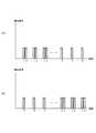
図9は、被検出物までの距離に対する受光素子32の検出信号の変化を示すグラフである。図9(A)は、受光素子32の検出信号の一例を示したグラフである。被検出物が近(短)距離にある場合、受光素子32は、全ての発光素子10A、10B、10Cからの反射光を受光し、全ての検出信号1、2、3を出力する。また、被検出物が中距離にある場合、受光素子32は、発光素子10B、10Cからの反射光を検出し、検出信号2、3を出力する。さらに、被検出物が遠距離にある場合、受光素子32は、発光素子10Bからの反射光だけを検出し、検出信号2を出力する。 FIG. 9 is a graph showing a change in the detection signal of the
図9(B)は、受光素子32の検出信号の他の一例を示したグラフである。また、受光素子32は、図9(B)に示す様に、各発光素子からの反射光の光量を基に光電変換して生じた電気エネルギーに基づく検出信号の信号値の加算値を出力してもよい。 FIG. 9B is a graph showing another example of the detection signal of the
具体的には、被検出物までの距離が近い(短距離)である場合、受光素子32は、全ての発光素子10A、10B、10Cからの反射光を受光し、図9(A)に示す全ての検出信号1、2、3の加算値に相当する検出信号を出力する。また、被検出物までの距離が少し遠い(中距離)場合、受光素子32は、発光素子10B、10Cからの反射光を受光し、図9(A)に示す検出信号2、3の加算値に相当する検出信号を出力する。更に、被検出物までの距離が遠い(遠距離)場合、受光素子32は、発光素子10Bからの反射光を受光し、図9(A)に示す検出信号2に相当する検出信号を出力する。 Specifically, when the distance to the object to be detected is short (short distance), the
受光素子32は、予め設定された検出信号の複数の閾値S1、S2、S3と反射光に対応する検出信号の信号値とを基に、被検出物までの距離を、短距離、中距離及び遠距離のうちいずれかであることを判断する。具体的には、受光素子32は、検出信号の信号値が閾値S1以上であって閾値S2未満である場合には、被検出物までの距離が遠距離と判断する。同様に、受光素子32は、検出信号の信号値が閾値S2以上であって閾値S3未満である場合には、被検出物までの距離が中距離と判断する。更に、受光素子32は、検出信号の信号値が閾値S3以上である場合には、被検出物までの距離が近距離と判断する。 The
なお、受光素子32は、反射光量が外光等のノイズを考慮して設定された閾値S1以下である場合、ドライバ回路により検出信号を出力しない様に設定されている。 The
この様に、第2の実施形態の近接センサ19Aによれば、被検出物によるタッチレスモーションが検出可能であるばかりでなく、近接センサ19Aの上面に対して垂直な方向(Z軸方向)における被検出物の距離も検出可能である。従って、Z軸方向の距離を検出するために、別のセンサを設ける必要がなく、部品点数を増やさなくて済む。 As described above, according to the
なお、本実施形態では、発光素子10A、10B、10Cは、横方向と縦方向が90°となる直角に配置されたが、距離だけを検出する場合には、特に面内における発光素子の位置関係は限定されず、任意に配置が可能である。 In the present embodiment, the
また、本実施形態では、遠距離、中距離、短距離の3つの距離を判別したが、受光素子による検出信号の信号レベル(受光量)に対し、複数のしきい値を設定しておくことで、より細かい距離の判別を行うことも可能である。例えば、「強」の発光量を有する発光素子10Bによる検出信号の信号レベルに対し、複数のしきい値を設定しておくことで、遠距離を2つ以上の距離に区別することも可能である。このことは、中距離、短距離においても同様である。 In this embodiment, the three distances of long distance, medium distance, and short distance are determined. However, a plurality of threshold values are set for the signal level (light reception amount) of the detection signal by the light receiving element. Thus, it is possible to determine a finer distance. For example, it is possible to distinguish a long distance into two or more distances by setting a plurality of threshold values for the signal level of the detection signal from the
(第3の実施形態)
第1の実施形態の近接センサでは、発光素子が実装される立体回路基板の凹部の壁面は、すり鉢状に形成されていた。第3の実施形態の近接センサでは、複数の発光素子がそれぞれ実装される立体回路基板の複数の凹部の壁面は、各発光素子から出射された光が受光素子に直接受光されない様に、受光素子に対して外側に傾く様に形成される。すなわち、立体回路基板の凹部の開口部は偏ったものとなる。(Third embodiment)
In the proximity sensor of the first embodiment, the wall surface of the concave portion of the three-dimensional circuit board on which the light emitting element is mounted is formed in a mortar shape. In the proximity sensor according to the third embodiment, the wall surfaces of the plurality of concave portions of the three-dimensional circuit board on which the plurality of light emitting elements are respectively mounted are arranged so that the light emitted from each light emitting element is not directly received by the light receiving element. It forms so that it may incline outside. That is, the opening of the recessed portion of the three-dimensional circuit board is biased.
図10は、第3の実施形態の近接センサ19Bにおける複数の発光素子10A、10B、10Cがそれぞれ実装される立体回路基板1の複数の凹部の形状、及び各発光素子10A、10B、10Cから出射される光の出射方向を示す図である。図10(A)は、近接センサ19Bの平面図である。図10(B)は、図10(A)の矢印C−C線方向の断面図である。第3の実施形態の近接センサ19Bは、立体回路基板1の凹部の壁面の形状を除き、第1の実施形態の近接センサ19と同一の構成を有する。 FIG. 10 shows the shapes of the plurality of concave portions of the three-
樹脂基板5に形成された凹部5aA、凹部5aB及び凹部5aCは、それぞれ焦点に位置する発光素子10A、10B、10Cからそれぞれ出射された光が反射して平行光に近づく様に、放物面に近い面に形成されている。この放物面は、各発光素子からの光が平行光となる様に、例えばパラボラ形状であることが好ましい。本実施形態では、凹部5aA、凹部5aBの中心軸は、それぞれ樹脂基板5の面に対して垂直なZ軸に対し、横方向の外側(図10(A)の左方向、右方向)に約30°傾いている。また、図10(B)には図示していないが、凹部5aCの中心軸は、Z軸に対し、縦方向の外側(図10(A)の上方向)に約30°傾いている。 The recesses 5aA, 5aB, and 5aC formed on the
この様に、凹部5aA、5aB、5aCは、外側に偏った開口部をそれぞれ有する。従って、発光素子10A、10B、10Cからそれぞれ出射された光は、外側に拡散しながらも、干渉することなく、被検出物に入射されることになる。これにより、近接センサ19Bは、光の干渉を抑えることができ、被検出物の誤検出を防止することができる。 In this way, the recesses 5aA, 5aB, and 5aC each have an opening that is biased outward. Therefore, the light emitted from each of the
なお、凹部5aA、凹部5aB、凹部5aCの中心軸は、図10(C)に示す様に、角方向の外側(図10(C)の右上方向、左下方向、右下方向)にそれぞれ向く様に傾いていてもよい。これにより、近接センサ19Bは、発光素子10A、10B、10Cからの光を干渉させない様に光を出射することができる。 As shown in FIG. 10C, the central axes of the recesses 5aA, the recesses 5aB, and the recesses 5aC are respectively oriented outward in the angular direction (upper right direction, lower left direction, and lower right direction in FIG. 10C). You may lean on. Accordingly, the
この様に、第3の実施形態の近接センサ19Bによれば、複数の発光素子から出射される光の干渉を抑制し、被検出物により反射された反射光がどの発光素子から出射されたものであるかを適切に識別することができる。 As described above, according to the
(第4の実施形態)
第1〜第3の実施形態の近接センサでは、発光素子が3つである場合を示したが、発光素子の数は3つ以上であればよく、その数は任意である。第4の実施形態では、基板の中央に受光素子が配置され、その周囲に4つの発光素子が配置された近接センサを示す。(Fourth embodiment)
In the proximity sensors of the first to third embodiments, the case where there are three light emitting elements is shown, but the number of light emitting elements may be three or more, and the number is arbitrary. The fourth embodiment shows a proximity sensor in which a light receiving element is arranged at the center of a substrate and four light emitting elements are arranged around the light receiving element.
図11は、第4の実施形態の近接センサ29Aにおける発光素子及び受光素子の配置を示す図である。図11(A)は、近接センサ29Aの平面図である。図11(A)に示す近接センサ29Aでは、凹部25A、25B、25C、25Dの壁面がそれぞれ横方向(図11(A)の左方向、右方向)あるいは縦方向(図11(A)の上方向、下方向)の外側に向く様に形成される。 FIG. 11 is a diagram illustrating the arrangement of light emitting elements and light receiving elements in the
また、図11(B)に示す近接センサ29Bでは、凹部35A、35B、35C、35Dの壁面がそれぞれ角方向(図11(B)の左方向、下方向、右方向、上方向)の外側に向く様に形成される。図11(B)は、第4の実施形態の変形例の近接センサ29Bの平面図である。 Further, in the
第4の実施形態における近接センサ29Aによれば、タッチレスモーションを検出する場合、横方向或いは縦方向に対して45°傾いた方向から被検出物が移動する際、受光素子32によって検出される検出信号の出力パターンが同じになる。従って、上下方向、左右方向、右斜め45°方向、左斜め45°方向、つまり4方向の検出能力を高めることができる。また、立体回路基板1の凹部の壁面が互いに外側に向いているので、4つの発光素子から出射される光の混合を抑えることができる。 According to the
以上、図面を参照しながら各種の実施形態について説明したが、本発明はかかる例に限定されないことは言うまでもない。当業者であれば、特許請求の範囲に記載された範疇内において、各種の変更例または修正例に想到し得ることは明らかであり、それらについても当然に本発明の技術的範囲に属するものと了解される。 While various embodiments have been described above with reference to the drawings, it goes without saying that the present invention is not limited to such examples. It will be apparent to those skilled in the art that various changes and modifications can be made within the scope of the claims, and these are naturally within the technical scope of the present invention. Understood.
例えば、上記実施形態では、1ショットレーザ輪郭除去法で立体回路基板が製造される場合を示したが、この方法に限らない。立体回路基板を製造する方法として、2度の射出成形を行って製造する2ショット法を用いてもよい。また、回路パターンに沿って、レーザを照射し、レーザ照射部のみにメッキを析出させることで回路を形成するLDS(Laser−Direct−Structuring)法を用いてもよい。 For example, in the above-described embodiment, the case where the three-dimensional circuit board is manufactured by the one-shot laser contour removal method is shown, but the present invention is not limited to this method. As a method of manufacturing the three-dimensional circuit board, a two-shot method of manufacturing by performing injection molding twice may be used. Alternatively, a laser-direct-structuring (LDS) method may be used in which a circuit is formed by irradiating a laser along a circuit pattern and depositing plating only on the laser irradiation portion.
本発明は、被検出物を検出する近接センサであって、あらかじめ発光部の発光タイミングを調整して基板の設計を簡単にし、被検出物を高精度に検出することができ、有用である。 The present invention is a proximity sensor that detects an object to be detected, and is useful because it can adjust the light emission timing of the light emitting unit in advance to simplify the design of the substrate and detect the object to be detected with high accuracy.
1 立体回路基板
5 基板
5a、5aA、5aB、5aC、5aD、25A、25B、25C、25D 凹部
5b 底面
5c 壁面
7 Cu薄膜
8 輪郭
9b Cuめっき層
10A、10B、10C、発光素子
14 Niめっき層
16 Auめっき層
17 接着剤
19、19A、19B、29A、29B 近接センサ
32 受光素子DESCRIPTION OF
Claims (8)
Translated fromJapanese基板と、
全てが直線に並ばずに前記基板の面に実装され、光を出射する少なくとも3つの発光部と、
前記少なくとも3つの発光部と所定の位置関係を構成して前記基板の面に実装され、前記発光部から出射されて前記被検出物で反射された反射光を受光する受光部と、
を備える近接センサ。A proximity sensor for detecting an object to be detected,
A substrate,
All are mounted on the surface of the substrate without being aligned in a straight line, and at least three light emitting units that emit light,
A light receiving unit configured to form a predetermined positional relationship with the at least three light emitting units and mounted on the surface of the substrate, and receiving reflected light emitted from the light emitting unit and reflected by the object to be detected;
Proximity sensor.
前記基板は、1ショットレーザ輪郭除去法で製造された立体回路基板である近接センサ。The proximity sensor according to claim 1,
The proximity sensor is a three-dimensional circuit board manufactured by a one-shot laser contour removal method.
前記少なくとも3つの発光部及び前記受光部は、それぞれ前記基板の表面に形成された凹部に実装される近接センサ。The proximity sensor according to claim 1 or 2,
Each of the at least three light emitting units and the light receiving unit is a proximity sensor mounted in a recess formed on a surface of the substrate.
前記受光部は、前記少なくとも3つの発光部から出射されて前記被検出物で反射された反射光の受光パターンを基に、前記被検出物の移動を検出する近接センサ。The proximity sensor according to any one of claims 1 to 3,
The light receiving unit is a proximity sensor that detects movement of the detected object based on a light receiving pattern of reflected light that is emitted from the at least three light emitting units and reflected by the detected object.
前記少なくとも3つの発光部から出射される光の発光量が異なり、
前記受光部は、前記反射された光の受光量をもとに、前記面に対して垂直方向の前記被検出物の距離を検出する近接センサ。The proximity sensor according to any one of claims 1 to 4,
The amount of light emitted from the at least three light emitting units is different,
The light receiving unit is a proximity sensor that detects a distance of the object to be detected in a direction perpendicular to the surface based on a received light amount of the reflected light.
前記少なくとも3つの発光部が載置される凹部は、前記受光部に対し、前記発光部から出射される光が外側を向く様に、前記外側に偏った開口部を有する近接センサ。The proximity sensor according to claim 3,
The concave sensor in which the at least three light emitting units are placed has an opening that is biased toward the outside so that light emitted from the light emitting unit faces outward with respect to the light receiving unit.
前記基板の面に、前記受光部及び3つの前記発光部が矩形の四隅となるように配置された近接センサ。It is a proximity sensor as described in any one of Claims 1-6,
A proximity sensor in which the light receiving unit and the three light emitting units are arranged at four corners of a rectangle on the surface of the substrate.
前記基板の面の中央に前記受光部が配置され、前記受光部の周囲に4つの前記発光部が配置された近接センサ。It is a proximity sensor as described in any one of Claims 1-6,
A proximity sensor in which the light receiving unit is arranged at the center of the surface of the substrate, and the four light emitting units are arranged around the light receiving unit.
Priority Applications (7)
| Application Number | Priority Date | Filing Date | Title |
|---|---|---|---|
| JP2012005554AJP2013145174A (en) | 2012-01-13 | 2012-01-13 | Proximity sensor |
| TW102100382ATW201337307A (en) | 2012-01-13 | 2013-01-07 | Proximity sensor |
| PCT/JP2013/000094WO2013105510A1 (en) | 2012-01-13 | 2013-01-11 | Proximity sensor |
| US14/371,750US9223054B2 (en) | 2012-01-13 | 2013-01-11 | Proximity sensor |
| CN201380005307.4ACN104054008B (en) | 2012-01-13 | 2013-01-11 | Proximity transducer |
| KR1020147019375AKR20140105566A (en) | 2012-01-13 | 2013-01-11 | Proximity sensor |
| EP13736429.5AEP2804022A4 (en) | 2012-01-13 | 2013-01-11 | PROXIMITY SENSOR |
Applications Claiming Priority (1)
| Application Number | Priority Date | Filing Date | Title |
|---|---|---|---|
| JP2012005554AJP2013145174A (en) | 2012-01-13 | 2012-01-13 | Proximity sensor |
Publications (1)
| Publication Number | Publication Date |
|---|---|
| JP2013145174Atrue JP2013145174A (en) | 2013-07-25 |
Family
ID=48781459
Family Applications (1)
| Application Number | Title | Priority Date | Filing Date |
|---|---|---|---|
| JP2012005554APendingJP2013145174A (en) | 2012-01-13 | 2012-01-13 | Proximity sensor |
Country Status (7)
| Country | Link |
|---|---|
| US (1) | US9223054B2 (en) |
| EP (1) | EP2804022A4 (en) |
| JP (1) | JP2013145174A (en) |
| KR (1) | KR20140105566A (en) |
| CN (1) | CN104054008B (en) |
| TW (1) | TW201337307A (en) |
| WO (1) | WO2013105510A1 (en) |
Cited By (10)
| Publication number | Priority date | Publication date | Assignee | Title |
|---|---|---|---|---|
| JP2015176473A (en)* | 2014-03-17 | 2015-10-05 | アルプス電気株式会社 | input device |
| JP2015179054A (en)* | 2014-03-20 | 2015-10-08 | 京セラディスプレイ株式会社 | display device |
| KR20150121950A (en)* | 2014-04-22 | 2015-10-30 | 엘지전자 주식회사 | Display apparatus for vehicle |
| US9891756B2 (en) | 2015-03-10 | 2018-02-13 | Lg Electronics Inc. | Vehicle display apparatus including capacitive and light-based input sensors |
| JP2019002794A (en)* | 2017-06-15 | 2019-01-10 | 日本精工株式会社 | Proximity sensor control method |
| JP2019519087A (en)* | 2016-03-12 | 2019-07-04 | ニンボー サニー オプテック カンパニー,リミテッド | Array imaging module and molded photosensitive assembly, and method of manufacturing the same for electronic devices |
| JP2019526168A (en)* | 2016-07-07 | 2019-09-12 | モレックス エルエルシー | Molded interconnect device and method of making the same |
| JP2019174125A (en)* | 2018-03-26 | 2019-10-10 | パイオニア株式会社 | Ranging device |
| JP2019174126A (en)* | 2018-03-26 | 2019-10-10 | パイオニア株式会社 | Ranging device |
| JP2021150671A (en)* | 2020-03-16 | 2021-09-27 | ローム株式会社 | Light receiving ICs, proximity sensors, and electronic devices |
Families Citing this family (12)
| Publication number | Priority date | Publication date | Assignee | Title |
|---|---|---|---|---|
| KR102138510B1 (en)* | 2013-08-27 | 2020-07-28 | 엘지전자 주식회사 | Electronic device for sensing proximity touch and controlling method thereof |
| US9525770B2 (en)* | 2014-03-26 | 2016-12-20 | Google Technology Holdings LLC | Portable electronic device with dual, diagonal proximity sensors and mode switching functionality |
| US9945948B2 (en)* | 2015-06-18 | 2018-04-17 | Nokia Technologies Oy | Method and apparatus for providing time-of-flight calculations using distributed light sources |
| KR102511622B1 (en)* | 2016-06-09 | 2023-03-17 | 엘지전자 주식회사 | Refrigerator |
| CN107884066A (en)* | 2017-09-29 | 2018-04-06 | 深圳奥比中光科技有限公司 | Optical sensor and its 3D imaging devices based on flood lighting function |
| KR102523975B1 (en) | 2017-10-11 | 2023-04-20 | 삼성전자주식회사 | Light source integrated light sensing system and electronic apparatus including the same |
| CN108132138A (en)* | 2017-11-23 | 2018-06-08 | 矽力杰半导体技术(杭州)有限公司 | Optical sensing module |
| TWI685670B (en)* | 2018-05-07 | 2020-02-21 | 新加坡商光寶科技新加坡私人有限公司 | Proximity sensor module with two emitters |
| JP7300850B2 (en)* | 2019-03-07 | 2023-06-30 | アズビル株式会社 | Detection device and clamping device |
| CN114765662A (en)* | 2021-01-13 | 2022-07-19 | 富士康(昆山)电脑接插件有限公司 | Sensing module |
| EP4198554A1 (en)* | 2021-12-15 | 2023-06-21 | STMicroelectronics (Research & Development) Limited | Assembly comprising a display screen and a proximity sensor |
| US20240102852A1 (en)* | 2022-09-22 | 2024-03-28 | Apple Inc. | Optical Proximity Sensor |
Family Cites Families (19)
| Publication number | Priority date | Publication date | Assignee | Title |
|---|---|---|---|---|
| JPS6249257A (en) | 1985-08-29 | 1987-03-03 | Ajiya Rika Kogyo Kk | Inspection paper set for quick qualitative inspection of vanillyl mandelate in urine and use thereof |
| JPS633474A (en) | 1986-06-23 | 1988-01-08 | Toshiba Corp | Reflection type light-coupled element |
| JPH01171053A (en) | 1987-12-25 | 1989-07-06 | Fujitsu Ltd | Terminal device control method |
| JP3265449B2 (en) | 1996-01-25 | 2002-03-11 | シャープ株式会社 | Distance sensor |
| JP3437709B2 (en)* | 1996-04-16 | 2003-08-18 | 株式会社東芝 | Three-dimensional wiring type optical coupling device and reflection type optical coupling device |
| JP3240941B2 (en) | 1996-11-18 | 2001-12-25 | 松下電器産業株式会社 | Hand gesture detection method and device |
| JP2000075046A (en)* | 1998-08-31 | 2000-03-14 | Rohm Co Ltd | Reflection-type sensor and rotary operation detector |
| JP2001188087A (en)* | 1999-12-28 | 2001-07-10 | Bandai Co Ltd | Sensor means and recognition device using the same |
| JP2002131051A (en)* | 2000-10-26 | 2002-05-09 | Stanley Electric Co Ltd | Distance detection device |
| US7718451B2 (en)* | 2003-02-28 | 2010-05-18 | Osram Opto Semiconductor Gmbh | Method for producing an optoelectronic device with patterned-metallized package body and method for the patterned metalization of a plastic-containing body |
| KR101058309B1 (en)* | 2006-01-13 | 2011-08-22 | 파나소닉 주식회사 | 3D circuit board and its manufacturing method |
| JP4769859B2 (en)* | 2006-02-28 | 2011-09-07 | 富士通株式会社 | Reflected light detection device, reflection characteristic determination device, and object detection device |
| DK1880718T3 (en)* | 2006-07-10 | 2011-11-21 | Pfleger R Chem Fab | Pharmaceutical composition for oral administration with controlled release of active substance in the small intestine and method of preparation thereof |
| JP4389911B2 (en)* | 2006-08-30 | 2009-12-24 | パナソニック電工株式会社 | Fingerprint image input device |
| JP5294757B2 (en) | 2007-09-28 | 2013-09-18 | 京セラ株式会社 | Sensor device using light receiving / emitting integrated element array |
| US8217482B2 (en)* | 2007-12-21 | 2012-07-10 | Avago Technologies General Ip (Singapore) Pte. Ltd. | Infrared proximity sensor package with reduced crosstalk |
| US8258453B2 (en)* | 2009-04-29 | 2012-09-04 | Intersil Americas Inc. | Long range proximity and/or motion detector with ambient light detection capabilities |
| US8304733B2 (en)* | 2009-05-22 | 2012-11-06 | Motorola Mobility Llc | Sensing assembly for mobile device |
| KR101091515B1 (en)* | 2009-09-14 | 2011-12-08 | 대성전기공업 주식회사 | Remote touch pad device of vehicle and control method of the same |
- 2012
- 2012-01-13JPJP2012005554Apatent/JP2013145174A/enactivePending
- 2013
- 2013-01-07TWTW102100382Apatent/TW201337307A/ennot_activeIP Right Cessation
- 2013-01-11CNCN201380005307.4Apatent/CN104054008B/ennot_activeExpired - Fee Related
- 2013-01-11EPEP13736429.5Apatent/EP2804022A4/ennot_activeWithdrawn
- 2013-01-11WOPCT/JP2013/000094patent/WO2013105510A1/enactiveApplication Filing
- 2013-01-11USUS14/371,750patent/US9223054B2/ennot_activeExpired - Fee Related
- 2013-01-11KRKR1020147019375Apatent/KR20140105566A/ennot_activeWithdrawn
Cited By (15)
| Publication number | Priority date | Publication date | Assignee | Title |
|---|---|---|---|---|
| JP2015176473A (en)* | 2014-03-17 | 2015-10-05 | アルプス電気株式会社 | input device |
| JP2015179054A (en)* | 2014-03-20 | 2015-10-08 | 京セラディスプレイ株式会社 | display device |
| KR20150121950A (en)* | 2014-04-22 | 2015-10-30 | 엘지전자 주식회사 | Display apparatus for vehicle |
| KR101655810B1 (en)* | 2014-04-22 | 2016-09-22 | 엘지전자 주식회사 | Display apparatus for vehicle |
| US9864469B2 (en) | 2014-04-22 | 2018-01-09 | Lg Electronics Inc. | Display apparatus for a vehicle |
| US9891756B2 (en) | 2015-03-10 | 2018-02-13 | Lg Electronics Inc. | Vehicle display apparatus including capacitive and light-based input sensors |
| JP2019519087A (en)* | 2016-03-12 | 2019-07-04 | ニンボー サニー オプテック カンパニー,リミテッド | Array imaging module and molded photosensitive assembly, and method of manufacturing the same for electronic devices |
| US11357112B2 (en) | 2016-07-07 | 2022-06-07 | Molex, Llc | Molded interconnect device |
| JP2019526168A (en)* | 2016-07-07 | 2019-09-12 | モレックス エルエルシー | Molded interconnect device and method of making the same |
| JP2019002794A (en)* | 2017-06-15 | 2019-01-10 | 日本精工株式会社 | Proximity sensor control method |
| JP2019174126A (en)* | 2018-03-26 | 2019-10-10 | パイオニア株式会社 | Ranging device |
| JP2019174125A (en)* | 2018-03-26 | 2019-10-10 | パイオニア株式会社 | Ranging device |
| JP2022159438A (en)* | 2018-03-26 | 2022-10-17 | パイオニア株式会社 | Ranging device |
| JP2022162080A (en)* | 2018-03-26 | 2022-10-21 | パイオニア株式会社 | Distance measuring device |
| JP2021150671A (en)* | 2020-03-16 | 2021-09-27 | ローム株式会社 | Light receiving ICs, proximity sensors, and electronic devices |
Also Published As
| Publication number | Publication date |
|---|---|
| US9223054B2 (en) | 2015-12-29 |
| CN104054008A (en) | 2014-09-17 |
| TW201337307A (en) | 2013-09-16 |
| KR20140105566A (en) | 2014-09-01 |
| US20150001414A1 (en) | 2015-01-01 |
| TWI563278B (en) | 2016-12-21 |
| WO2013105510A1 (en) | 2013-07-18 |
| EP2804022A4 (en) | 2015-07-15 |
| CN104054008B (en) | 2016-11-23 |
| EP2804022A1 (en) | 2014-11-19 |
Similar Documents
| Publication | Publication Date | Title |
|---|---|---|
| JP2013145174A (en) | Proximity sensor | |
| JP5886158B2 (en) | Multi-directional proximity sensor | |
| JP5327980B2 (en) | Optical proximity sensor with improved shield and lens | |
| EP3786707B1 (en) | Projection module and terminal | |
| US20130019461A1 (en) | Opto-electronic modules and methods of manufacturing the same and appliances and devices comprising the same | |
| JP6436296B2 (en) | 3D circuit board and sensor module using the 3D circuit board | |
| KR20100105486A (en) | Photoelectric transmitting or receiving device and manufacturing method thereof | |
| US10734366B2 (en) | Opto-electronic module for emitting light of variable intensity distribution | |
| US20160076724A1 (en) | Light source support with integral connector | |
| JP6489843B2 (en) | Light source unit | |
| JPWO2017098584A1 (en) | Photo reflector | |
| TWI755046B (en) | 3d sensing device, lighting module and control method thereof | |
| JP2013128013A (en) | Method of manufacturing three-dimensional circuit board, three-dimensional circuit board, proximity sensor, and light-emitting device | |
| JP2011048468A (en) | Optical pointing device and electronic equipment loaded with the same device | |
| US7714835B2 (en) | Opto-electronic input device, method of manufacturing such a device and method of measuring the movement of an object by means of such a device | |
| CN111050029A (en) | Imaging module and electronic device | |
| CN219959007U (en) | Optical sensing device | |
| CN108603645B (en) | Method for producing a holding device for a light module of a lighting device of a motor vehicle | |
| TWM648161U (en) | Optical sensing device | |
| KR20250145161A (en) | Sensor module and camera device comprising the same | |
| KR20240124017A (en) | Light output device and camera device comprising the same | |
| CN112637446A (en) | Camera assembly of electronic equipment and electronic equipment | |
| TWM356351U (en) | Circuit board module for tracking optical location |
Legal Events
| Date | Code | Title | Description |
|---|---|---|---|
| RD04 | Notification of resignation of power of attorney | Free format text:JAPANESE INTERMEDIATE CODE: A7424 Effective date:20131225 |