JP2013137713A - Memory controller, memory system, and memory write method - Google Patents
Memory controller, memory system, and memory write methodDownload PDFInfo
- Publication number
- JP2013137713A JP2013137713AJP2011289128AJP2011289128AJP2013137713AJP 2013137713 AJP2013137713 AJP 2013137713AJP 2011289128 AJP2011289128 AJP 2011289128AJP 2011289128 AJP2011289128 AJP 2011289128AJP 2013137713 AJP2013137713 AJP 2013137713A
- Authority
- JP
- Japan
- Prior art keywords
- data
- write
- channel
- unit
- memory
- Prior art date
- Legal status (The legal status is an assumption and is not a legal conclusion. Google has not performed a legal analysis and makes no representation as to the accuracy of the status listed.)
- Pending
Links
Images


Classifications
- G—PHYSICS
- G06—COMPUTING OR CALCULATING; COUNTING
- G06F—ELECTRIC DIGITAL DATA PROCESSING
- G06F11/00—Error detection; Error correction; Monitoring
- G06F11/07—Responding to the occurrence of a fault, e.g. fault tolerance
- G06F11/08—Error detection or correction by redundancy in data representation, e.g. by using checking codes
- G06F11/10—Adding special bits or symbols to the coded information, e.g. parity check, casting out 9's or 11's
- G06F11/1008—Adding special bits or symbols to the coded information, e.g. parity check, casting out 9's or 11's in individual solid state devices
- G06F11/1048—Adding special bits or symbols to the coded information, e.g. parity check, casting out 9's or 11's in individual solid state devices using arrangements adapted for a specific error detection or correction feature
- H—ELECTRICITY
- H03—ELECTRONIC CIRCUITRY
- H03M—CODING; DECODING; CODE CONVERSION IN GENERAL
- H03M13/00—Coding, decoding or code conversion, for error detection or error correction; Coding theory basic assumptions; Coding bounds; Error probability evaluation methods; Channel models; Simulation or testing of codes
- H03M13/03—Error detection or forward error correction by redundancy in data representation, i.e. code words containing more digits than the source words
Landscapes
- Engineering & Computer Science (AREA)
- Theoretical Computer Science (AREA)
- Physics & Mathematics (AREA)
- Quality & Reliability (AREA)
- General Engineering & Computer Science (AREA)
- General Physics & Mathematics (AREA)
- Probability & Statistics with Applications (AREA)
- Techniques For Improving Reliability Of Storages (AREA)
- Memory System (AREA)
Abstract
Translated fromJapaneseDescription
Translated fromJapanese本実施形態は、メモリコントローラ、メモリシステムおよびメモリ書込み方法に関する。 The present embodiment relates to a memory controller, a memory system, and a memory writing method.
NANDフラッシュメモリ(以下、NANDメモリという)を用いたSSD(Solid State Drive)システムでは、一般に、信頼性確保のために記憶するデータとともに誤り訂正符号における冗長データをNANDメモリへ格納する。SSDシステムのメモリコントローラでは、複数のチャネルを有し、各チャネルで並行してNANDメモリの読み書きを実施する場合がある。各チャネルは、一般にNANDメモリのメモリチップにそれぞれ対応している。 In an SSD (Solid State Drive) system using a NAND flash memory (hereinafter referred to as a NAND memory), redundant data in an error correction code is generally stored in a NAND memory together with data stored for ensuring reliability. The memory controller of the SSD system has a plurality of channels, and the NAND memory may be read and written in parallel in each channel. Each channel generally corresponds to a memory chip of a NAND memory.
本実施形態は、チャネル利用効率および書込み速度を向上させることができるメモリコントローラ、メモリシステムおよびメモリ書込み方法を提供する。 The present embodiment provides a memory controller, a memory system, and a memory writing method capable of improving channel utilization efficiency and writing speed.
本願発明の一態様によれば、複数のチャネルを有し、チャネルごとに不揮発性メモリへの書込みを行うメモリインタフェースと、データバッファと、書込みデータに基づいて誤り訂正符号化処理を実施して冗長データを生成するECCエンコーダと、書込みデータフォーマットに基づいて書込みデータおよび冗長データに対してチャネルを割付けるチャネル割付け部と、書込みデータをデータバッファへ格納するとともに当該書込みデータをECCエンコーダへ入力する書込みデータ受信処理部と、チャネル割付け結果に基づいてデータバッファに格納された書込みデータと冗長データとをメモリインタフェースへ転送するチャネルスケジューラと、を備える。 According to one aspect of the present invention, a redundant memory is provided which has a plurality of channels and performs error correction coding processing based on write data, a memory interface for writing to the nonvolatile memory for each channel, and a data buffer. An ECC encoder that generates data, a channel allocation unit that allocates channels to write data and redundant data based on the write data format, and a write that stores the write data in the data buffer and inputs the write data to the ECC encoder A data reception processing unit; and a channel scheduler that transfers write data and redundant data stored in the data buffer to the memory interface based on a channel allocation result.
複数のチャネルを有するSSDシステムでは、メモリチップ単位の故障時にデータを復元可能とするために、誤り訂正符号の元となるデータを複数のチャネルに分散させて書き込むチャネル間ECC(Error Check and Correct)が導入されることがある。この様なSSDシステムでは、チャネル間ECCを実施する場合、ECC生成単位分の書込みデータがそろうのを待ってから書込みを行うことを基本としている。 In an SSD system having a plurality of channels, an error check and correct (ECC) between channels is written in which data serving as an error correction code is distributed and written to a plurality of channels in order to be able to restore data when a failure occurs in units of memory chips. May be introduced. In such an SSD system, when performing the inter-channel ECC, it is basically based on writing after waiting for the write data for the ECC generation unit to be aligned.
このため、チャネル間ECCを実施する場合、(1)ECCデータ(誤り訂正符号化における冗長データ)を生成してから書き込む、(2)ECCデータを生成しながら書き込む、のどちらかの方法が採用され得る。(1)の場合、書込みデータが揃っても、ECCデータの生成が終了するまで当該ECCデータの生成の元になる書込みデータをNANDメモリへ書込むことができない。このため、書込み速度が低下するという問題がある。 For this reason, when performing inter-channel ECC, either (1) ECC data (redundant data in error correction coding) is generated and written, or (2) ECC data is written while being generated. Can be done. In the case of (1), even if write data is prepared, the write data that is the source of generation of the ECC data cannot be written into the NAND memory until the generation of the ECC data is completed. For this reason, there is a problem that the writing speed is lowered.
(2)の場合、ECCデータの生成処理に入力する順にNANDメモリに転送することにより、ECCデータと当該ECCデータの対応を管理するため、ECCデータにかかわる全てのチャネル(ECCデータと当該ECCデータに対応する書込みデータとを書き込む全てのチャネル)が空くのを待ってからNANDメモリへの書込みを実施することになる。このため、チャネルごとに見た場合、空き時間が生じることとなり非効率である。また、ECCデータとECCデータにかかわる全ての書込みデータの書込みが終了するまで書込み対象のチャネルは解放されない。このため、システムとして優先されるべきリードコマンドが発生しても、対応するチャネルが使用中であり割り込めない確率が増え、システム全体の性能を落とすこととなる。 In the case of (2), in order to manage the correspondence between the ECC data and the ECC data by transferring the data to the NAND memory in the order of input to the ECC data generation process, all the channels (ECC data and the ECC data related to the ECC data) are managed. The writing to the NAND memory is performed after waiting for all the channels for writing the write data corresponding to (1) to become free. For this reason, when it sees for every channel, an idle time will arise and it is inefficient. Further, the channel to be written is not released until the writing of the ECC data and all the write data related to the ECC data is completed. For this reason, even if a read command that should be prioritized as a system occurs, the probability that the corresponding channel is in use and cannot be interrupted increases, and the performance of the entire system is degraded.
以下に添付図面を参照して、実施形態にかかるメモリコントローラ、メモリシステムおよびメモリ書込み方法を詳細に説明する。なお、この実施形態により本発明が限定されるものではない。 Hereinafter, a memory controller, a memory system, and a memory writing method according to embodiments will be described in detail with reference to the accompanying drawings. In addition, this invention is not limited by this embodiment.
図1は、実施の形態にかかるメモリシステムの構成例を示すブロック図である。図1に示すように、本実施の形態のメモリシステム3は、メモリコントローラ1とNANDメモリ(不揮発性メモリ)2を備える。メモリシステム3は、ホスト4と接続可能であり、図1ではホスト4と接続された状態を示している。ホスト4は、例えば、パーソナルコンピュータ、携帯端末などの電子機器である。 FIG. 1 is a block diagram of a configuration example of the memory system according to the embodiment. As shown in FIG. 1, the
NANDメモリ2は、データを不揮発に記憶する不揮発性メモリであり、4個のメモリチップ(メモリ21−1〜21−4)で構成されている。ここでは、NANDメモリ2を構成するメモリチップの数を4としているが、メモリチップの数はこれに限定されない。また、ここでは、不揮発性メモリとしてNANDメモリ2を用いる例を説明するが、NANDメモリ以外の記憶手段を用いてもよい。 The
メモリコントローラ1は、ホスト4からの書込み要求(ライトコマンド)に従ってNANDメモリ2への書込みを制御し、またホスト4からの読出し要求(リードコマンド)に従ってNANDメモリ2からの読出しを制御する。メモリコントローラ1は、リードコマンド受信処理部(Read Command Acceptor)11、ライトコマンド受信処理部(Write Command Acceptor)12、書込みデータ受信処理部(Write Data Acceptor)13、リードコマンド発行部(Read Commander)14、誤り訂正符号生成部(ECC Generator)15、チャネルスケジューラ(Channel Scheduler)16、NANDI/F(メモリインタフェース)17、およびデータバッファ(Data Buffer)18を備える。 The
NANDI/F17は、NANDメモリ2への書込みや読出しを直接制御するコントローラである。NANDI/F17は、メモリチップに対応する数のチャネル制御部(Channel)171−1〜171−4を有し、チャネル制御部171−1〜171−4はそれぞれ対応するメモリ21−1〜21−4に対する書込みや読出しを制御する。チャネル制御部171−1〜171−4は、並行してNANDメモリ2への書込みや読出しを行うことができる。ここでは、NANDI/F17は、NANDメモリ2のメモリチップの数に合わせて4つのチャネルを有しているが、メモリチップの数が4以外の場合はメモリチップの数のチャネルを有するようにすればよい。なお、以下、チャネル制御部171−i(i=1,2,…,4)に対応するチャネルをCH#iと表記する。 The NAND I /
リードコマンド受信処理部11は、ホスト4から読出し対象データのアドレスを含む読出し要求を受信すると、リードコマンド発行部14へ読出し要求を通知する。リードコマンド発行部14は、ホスト4から要求された読出し対象データのアドレスをNANDメモリ上のアドレスに変換し、変換したアドレスを含むリードコマンドを発行してチャネルスケジューラ16へ通知する。 When the read command reception processing unit 11 receives a read request including the address of the read target data from the
ライトコマンド受信処理部12は、ホスト4から書込みデータのアドレスを含むライトコマンドを受信すると、誤り訂正符号生成部15へライトコマンドおよび書込みデータのアドレスを通知する。書込みデータ受信処理部13は、ホスト4から書込みデータを受信すると、当該データを誤り訂正符号生成部15へ入力するとともにデータバッファ18へ格納する。 When receiving a write command including the address of the write data from the
誤り訂正符号生成部15は、書込みデータに対してチャネル割付けを実施し、チャネル割付け結果と入力された書込みデータとに基づいて誤り訂正符号化処理を実施する。本実施の形態では、誤り訂正符号の生成の元になるデータが複数のチャネルに分散して配置される(複数のメモリチップに分散して格納される)ページ間ECCを実施する。また、誤り訂正符号生成部15は、チャネル割付け結果に基づいて書込みデータに対応するNANDメモリ2上のアドレスを含むライトコマンドを発行し、チャネルスケジューラ16へ通知する。 The error correction
チャネルスケジューラ16は、リードコマンド発行部14から発行されたリードコマンドに基づいて、読出し対象のデータが格納されているメモリ21−1〜21−4に対応するチャネル制御部171−1〜171−4へ当該データを読出すよう指示する。また、チャネルスケジューラ16は、誤り訂正符号生成部15から発行されたライトコマンドに基づいて、データバッファ18に格納されている書込みデータを、当該書込みデータに対応するNANDI/F17のチャネル制御部171−1〜171−4へ転送する。 The
図1に、白抜き矢印で、本実施の形態の書込みデータの流れを示している。本実施の形態では、図1の白抜き矢印で示したように、誤り訂正符号生成部15へ入力されるとともにデータバッファ18経由でNANDI/F17へ転送される。 FIG. 1 shows the flow of write data according to the present embodiment with white arrows. In this embodiment, as indicated by the white arrow in FIG. 1, the error correction
なお、本実施の形態では、NANDメモリ2への書込み処理について主として説明するため、図1では、データのフローについては、書込み方向の矢印を示し、また読出し処理に関する構成要素は一部しか示していないが、読出し時には、逆の方向(NANDメモリ2からメモリコントローラ1へ向かう方向)のデータフローとなる。読出しに関する処理や構成に特に制約はないが、例えば、チャネル制御部171−1〜171−4によりNANDメモリ2から読み出されたデータおよび誤り訂正符号は一旦データバッファ18に格納され、誤り訂正処理後のデータがホスト4へ転送される。 In the present embodiment, the write process to the
次に、本実施の形態の書込み処理について詳細に説明する。図2は、本実施の形態の誤り訂正符号生成部15の構成例を示す図である。図2に示すように、本実施の形態の誤り訂正符号生成部15は、チャネル割付け部(Channel Allocator)51、ライトコマンド発行部(Write Commander)52およびチャネル間ECCエンコーダ(Inter−Channel ECC Encoder)(ECC エンコーダ)53を備える。 Next, the writing process of the present embodiment will be described in detail. FIG. 2 is a diagram illustrating a configuration example of the error correction
図3は、チャネル割付け部51の構成例を示す図である。図3に示すように、チャネル割付け部51は、チャネル算出部(Channel Calculator)511を備える。チャネル算出部511は、ライトコマンド受信処理部12からライトコマンドを受信すると、チャネル数(Channel Number)と誤り訂正符号の配置(ECC Destination)とに基づいて、書込みデータ(書込みデータのアドレス)に割付けるチャネルとNANDメモリ2上のアドレスを計算し、チャネルとアドレスを割付け情報(割付け結果)としてライトコマンド発行部52へ出力する。また、チャネル算出部511は、ECC生成通知(ECC Ready)を受信すると、ECCデータに対して割付けるチャネルとNANDメモリ2上のアドレスを計算して割付け情報としてライトコマンド発行部52へ出力する。 FIG. 3 is a diagram illustrating a configuration example of the
誤り訂正符号の配置とはNANDメモリ2格納の際のデータフォーマットを示し、誤り訂正符号と当該誤り訂正符号に対応する書込みデータのNANDメモリ2上の記憶位置を決定するための規則を示す。ここで、1つの誤り訂正符号と当該誤り訂正符号に対応する書込みデータとを誤り訂正単位データと呼ぶこととし、誤り訂正単位データのサイズを示す単位を誤り訂正単位と呼ぶこととする。誤り訂正符号の配置は、誤り訂正単位データを書込むNANDメモリ2の書込み領域における誤り訂正符号の配置を示す。例えば、チャネル数が4で3ページ分のデータに基づいて1ページ分の1つの誤り訂正符号を生成する場合に、誤り訂正単位データは4ページとなる。1つの誤り訂正単位データ内の書込みデータを1ページ分ずつ各チャネルに分散させるとすると、CH#1〜CH#4のうちいずれか1つが誤り訂正符号を書込むチャネルとなり、他のチャネルは書込みデータを書込むチャネルとなる。この場合には、誤り訂正符号の配置は、3ページの書込みデータをどのチャネルに書込むかを指定する情報と、どのチャネルに誤り訂正符号を書込こむかを指定する情報と、を含む。CH#1〜CH#4のうち誤り訂正符号を書込むチャネルは、固定でもよいし固定でなくてもよい。なお、誤り訂正符号の配置の具体例については後述する。 The arrangement of the error correction code indicates a data format when the
なお、本実施の形態では、チャネル間ECCを実施するが、誤り訂正符号生成部15に入力されたデータが、複数のチャネルに分散されて配置されるためには、チャネル割付け部51は、誤り訂正符号生成部15に入力されるデータの順序を把握する必要がある。ここでは、書込みデータ受信処理部13が受信した順に誤り訂正符号生成部15にデータが入力されるとし、チャネル割付け部51は、データバッファ18に格納された順に誤り訂正符号生成部15にデータが入力されるとしてチャネル割付けを行う。書込みデータ受信処理部13が受信したデータの順序と誤り訂正符号生成部15へ入力するデータの順序を異なるように構成する場合は、チャネル割付け部51は、誤り訂正符号生成部15へ入力するデータの順序を示す規則を保持しておき、この規則に基づいてチャネル割付けを行えばよい。 In this embodiment, the inter-channel ECC is performed. However, in order for the data input to the error correction
図4は、チャネル間ECCエンコーダ53の構成例を示す図である。図4に示すように、チャネル間ECCエンコーダ53は、バッファ管理部(Buffer Manager)531、スタート検出部(Start Detector)532、ECC計算部(ECC Calculator)533、エンド検出部(End Detector)534およびECCバッファ(ECC Buffer)535を備える。 FIG. 4 is a diagram illustrating a configuration example of the
スタート検出部532は、誤り訂正単位データの開始位置、すなわち1つのECCデータに対応する誤り訂正符号化処理の開始を検出する。スタート検出部532は、ECC処理開始要求(ECC Request)をチャネル割付け部51またはライトコマンド受信処理部12から受けると、誤り訂正単位データのデータ数(Ecc-unit Number)、符号化カウンタ値(Encoded Counter)、空き領域情報(Vacant Area)に基づいて、入力される書込みデータについて誤り訂正単位データの開始を検出する。誤り訂正単位データの開始を検出すると、スタート検出部532は、ECCバッファ535上の格納開始アドレス(Start Address:これから生成する誤り訂正符号を格納する領域の開始アドレス)を求め、ECC計算部533へ通知する。誤り訂正単位データのデータ数は、誤り訂正単位データの書込みデータのサイズを表し、ここではページ数でサイズを示すとする。符号化カウンタ値は、ECC計算部533により処理されたデータ数をカウントするカウンタ値であり、ここではページ単位でカウントするとする。空き領域情報は、ECCバッファ535上の空き領域を示す情報である。 The
ECC計算部533は、入力された書込みデータに基づいて誤り訂正符号化処理により冗長データを生成し、生成した冗長データをECCデータとしてECCバッファ535へアドレス(スタート検出部532から通知された格納開始アドレス)を指定してECCバッファ535へ格納する。また、ECC計算部533は、符号化処理の中間状態をECCバッファ535の対応する格納領域へ書込み、入力された書込みデータを符号化処理へ反映させるごとに中間時状態を更新するとともに符号化カウンタ値を更新する。また、ECC計算部533は、スタート検出部532から格納開始アドレスが通知された場合には、処理を初期化してECCバッファ535へ格納するアドレスを通知された格納開始アドレスへ変更する。なお、ここでは、ページ単位で書込みデータが入力されるとし、符号化カウンタ値はページごとに更新される。 The
エンド検出部534は、誤り訂正単位データのデータ数および符号化カウンタ値に基づいて入力される書込みデータについて1つのECCデータに対応する誤り訂正符号化処理の終了を検出する。エンド検出部534は、誤り訂正単位データの終了を検出した場合、誤り訂正単位データの終了したことを示すECC生成通知(ECC Ready)を、当該誤り訂正単位データが格納されたECCバッファ535上のアドレス(ECC Address)とともにチャネル割付け部51へ出力する。 The
バッファ管理部531は、ECCデータの書込み完了通知(ECC Write Done)と当該ECCデータのアドレスとに基づいて、ECCバッファ535上の空き領域情報を更新する。すなわち、バッファ管理部531は、ECCデータの書込み完了通知を受信したECCデータが格納されていたECCバッファ535上の領域を空き領域に変更する。ECCデータの書込み完了通知(ECC Write Done)は、チャネルスケジューラ16が発行してもよいし、ライトコマンド発行部52が発行してもよい。 The
例えば、誤り訂正単位データが3ページの書込みデータと1ページのECCデータで生成されるとする。書込み処理の開始時には、スタート検出部532は、入力された最初のデータが誤り訂正単位データの開始であると判断し、エンド検出部534は、符号化カウンタ値に基づいて3ページのデータの符号化処理が終了すると誤り訂正単位データの終了を検出する。その後、スタート検出部532は、前の誤り訂正単位データが終了すると次の誤り訂正単位データの開始と判断する。 For example, it is assumed that error correction unit data is generated with three pages of write data and one page of ECC data. At the start of the writing process, the
なお、スタート検出部532による誤り訂正単位データの開始位置の検出、およびエンド検出部534による誤り訂正単位データの終了位置の検出方法は、前述の例に限定されず、どのような方法で実施してもよい。 The method for detecting the start position of the error correction unit data by the
図5は、ライトコマンド発行部52の構成例を示す図である。図5に示すように、ライトコマンド発行部52は、解読部(Decoder)521、受信処理部(Acceptor)522〜525およびコマンド発行部(Commander)526を備える。 FIG. 5 is a diagram illustrating a configuration example of the write
解読部521は、チャネル割付け部51から入力される割付け情報を解読し、割付け情報が通知されたデータについてはNANDメモリ2への書込み準備が完了したと判断し、割付け情報により通知された書込み先のチャネルに対応する受信処理部522〜525に書込み先のアドレスを通知する。受信処理部522,523,524,525は、それぞれCH#1,CH#2,CH#3,CH#4に対応する処理を実施する。例えば、解読部521は、チャネル割付け部51からCH#1を書込み先として指定する割付け情報を受け取った場合、CH#1に対応する受信処理部522へ当該割付け情報で指定されたアドレスを通知する。 The
受信処理部522〜525は、解読部521から通知されたアドレスを、保持しているアドレス数がチャネル書込み処理単位(Channel Write−Unit)に対応する数となるまで保持する。チャネル書込み処理単位は、メモリコントローラ1がNANDメモリ2に対して、書込みのために一度にデータを転送するデータ(書込み処理単位)の1チャネル当たりのデータサイズを示す単位である。保持しているアドレス数がチャネル書込み処理単位に対応する数となると、受信処理部522〜525は、チャネル書込み処理単位に対応する数のアドレスをコマンド発行部526へ入力する。なお、図5では、書込み処理単位を各チャネル4ページずつの16ページとし、チャネルごとにアドレスを4つ保持している例を示しているが、チャネル書込み処理単位はこれに限定されない。 The
コマンド発行部526は、受信処理部522〜525から受け取ったアドレスに基づいて、1つの書込み処理単位のアドレスが揃った場合に、当該書込み処理単位に対応するライトコマンドをアドレスパケット(書込み先のチャネルとアドレスを含む)とともに発行する。 When the address of one write processing unit is prepared based on the addresses received from the
チャネルスケジューラ16は、コマンド発行部526から発行されたライトコマンドに基づいて書込み対象の書込みデータまたはECCデータをデータバッファ18またはECCバッファ535から読出しNANDI/F17へ転送してNANDメモリ2への書込みを行う。すなわち、チャネルスケジューラ16は、書込み処理単位でNANDI/F17へデータを転送する。この際、データバッファ18上の書込みデータの格納位置、およびECCバッファ535上のECCデータの格納位置は、ライトコマンドとともにチャネル割付け部51から通知されてもよいし、メモリコントローラ2の図示しない全体制御部等からデータバッファ18上の書込みデータの格納位置、およびECCバッファ535上のECCデータの格納位置が通知されてもよい。 The
なお、一般にNANDメモリでは複数チャネルのデータで書込み処理単位が構成される。例えば、4チャネルの場合に、各チャネル4ページずつの計16ページ分を書込み処理単位とする。本実施の形態では、通常と同様に複数チャネルのデータで書込み処理単位を構成してもよいし、書込み処理単位を複数チャネルのデータで構成せずに、チャネルごとにライトコマンドを発行するようにしてもよい。また、さらに、チャネルごとにページ単位でライトコマンドを発行するようにしてもよい(すなわち、書込み処理単位を1ページとする)。 In general, in a NAND memory, a write processing unit is composed of data of a plurality of channels. For example, in the case of 4 channels, a total of 16 pages, 4 pages for each channel, is set as a write processing unit. In this embodiment, a write processing unit may be configured with data of multiple channels as usual, or a write command may be issued for each channel without configuring the write processing unit with data of multiple channels. May be. Furthermore, a write command may be issued for each channel in units of pages (that is, the write processing unit is one page).
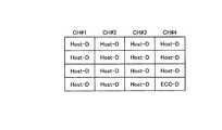
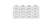
また、書込み処理単位と誤り訂正単位は同じであってもよいし、異なっていてもよい。図6〜9は、本実施の形態のNANDメモリ2へ書込むデータフォーマット(誤り訂正符号の配置)例を示す図である。図6〜9において、Host−Dは1ページのホストデータを示し、ECC−Dは、ECCデータを示している。図6、7は、書込み処理単位と誤り訂正単位が一致する例を示しており、図6は、書込み処理単位および誤り訂正単位が8ページの例を示し、図7は、書込み処理単位および誤り訂正単位が16ページの例を示している。なお、図6または図7に示すフォーマットを繰り返すようにしてもよいし、書込み処理単位内のECC−Dの配置を固定せず変更可能としてもよい。 Further, the write processing unit and the error correction unit may be the same or different. 6 to 9 are diagrams showing examples of the data format (arrangement of error correction codes) to be written into the
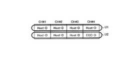
図8、9は、書込み処理単位と誤り訂正単位が一致しない例を示している。図8は、書込み処理単位が誤り訂正単位より小さい例を示しており、誤り訂正単位が8ページであり、書込み処理単位が4ページである。図8の例では、1つの誤り訂正単位は、書込み処理単位U1、U2の2つを含む。図9は、書込み処理単位が誤り訂正単位より大きい例を示しており、誤り訂正単位が8ページであり、書込み処理単位が16ページである。このように、誤り訂正単位は書込み処理単位より大きくてもよいし小さくてもよいが、本実施の形態では誤り訂正単位は書込み処理単位より大きい場合に、より効率的な書込みが実施できる。また、前述したように、書込み処理単位を1ページとしてもよい。 8 and 9 show examples in which the write processing unit and the error correction unit do not match. FIG. 8 shows an example in which the write processing unit is smaller than the error correction unit, where the error correction unit is 8 pages and the write processing unit is 4 pages. In the example of FIG. 8, one error correction unit includes two write processing units U1 and U2. FIG. 9 shows an example in which the write processing unit is larger than the error correction unit, where the error correction unit is 8 pages and the write processing unit is 16 pages. As described above, the error correction unit may be larger or smaller than the write processing unit, but in this embodiment, more efficient writing can be performed when the error correction unit is larger than the write processing unit. Further, as described above, the write processing unit may be one page.
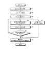
次に、本実施の形態の書込み動作について説明する。図10は、本実施の形態のメモリコントローラ1におけるNANDメモリ2への書込み手順の一例を示すフローチャートである。なお、ここでは説明の簡略化のため、1つの誤り訂正単位データをNANDメモリ2へ書き込む例を示し、また誤り訂正単位が書込み処理単位より大きい例を示す。まず、メモリコントローラ1のライトコマンド受信処理部12は、ホストから書込み要求(ライトコマンド)を受信(ステップS1)し、ホストデータ(ホストから送信された書込みデータ)を受信する(ステップS2)。 Next, the write operation of this embodiment will be described. FIG. 10 is a flowchart showing an example of a write procedure to the
チャネル割付け部51は、ホストデータに対してチャネル割付けを行う(ステップS3)。また、ホストデータは誤り訂正符号生成部15に入力される(ステップS4)。誤り訂正符号生成部15は、入力されたホストデータに基づいてECCデータ(中間状態を含む)を生成する(ステップS5)。そして、誤り訂正符号生成部15は、誤り訂正単位データ分のデータを処理したか否かを判断する(ステップS6)。誤り訂正単位データ分のデータを処理した場合(ステップS6 Yes)には、生成されたECCデータは、チャネルスケジューラ16およびNANDI/F17により、書込み処理単位でNANDメモリ2への書込みが実施され(ステップS8)、書込み処理を終了する。NANDI/F17は、転送されたデータをチャネルごとにNANDメモリ2へ書込む。 The
一方、誤り訂正単位データ分のデータを処理していない場合(ステップS6 No)、ステップS4へ戻る。また、ステップS3の後、ステップS4と並行して、チャネルスケジューラ16が、誤り訂正符号生成部15からライトコマンドを受信することにより書込み処理単位のデータに対するチャネル割付けの終了を検知すると、対応する書込み処理単位のホストデータをデータバッファ18から読み出しNANDI/F17へ転送する(ステップS7)。 On the other hand, when data for error correction unit data is not processed (No in step S6), the process returns to step S4. Further, after step S3, in parallel with step S4, when the
なお、2以上の誤り訂正単位データをNANDメモリ2へ書込む場合は、ステップS2〜ステップS8を繰り返す。 When writing two or more error correction unit data into the
以上説明したように、本実施の形態では、誤り訂正符号化処理とNANDI/Fへのデータ転送が並行して行われる。このため、書込み速度を向上させることができる。 As described above, in this embodiment, error correction coding processing and data transfer to the NAND I / F are performed in parallel. For this reason, the writing speed can be improved.
本実施の形態の効果を、図を用いて説明する。図11は、書込み処理単位を1ページとする場合のNANDメモリ2への書込みの順序の一例を示す図である。Host−D#iは、1ページのホストデータを示し、iは誤り訂正符号生成部15へ入力される順序を示す。すなわち、Host−D#1,Host−D#2,Host−D#3,…の順に誤り訂正符号生成部15へ入力されるとする。図11の(WEj)(j=1,2,3,4)は各ホストデータについてのNANDメモリ2への書込みが終了した順序を示し、(WE1)、(WE2)、(WE3)、(WE4)の順に書込みが終了したことを示す。すなわち、図11の例では、Host−D#3、Host−D#2、Host−D#1、Host−D#4の順に書込みが終了している。図11の例では、誤り訂正単位は8ページとしている。 The effect of this embodiment will be described with reference to the drawings. FIG. 11 is a diagram illustrating an example of the order of writing to the
従来は、誤り訂正符号化処理への入力順とNANDメモリ2への書込み順を整合させるため、誤り訂正単位データを書込む全てのチャネルが空くのを待ち、また誤り訂正単位データを書込みが終了するまで誤り訂正単位データを書込むチャネルを解放しない。したがって、図11のように、Host−D#3、Host−D#2、Host−D#1、Host−D#4の順に書込みが完了しても、従来の方法では、次の書込みデータHost−D#5を書込むCH#1が空くまでCH#3やCH#2の書込みは実施できない。これに対し、本実施の形態では、書込み処理単位のデータが揃えば、NANDメモリ2への書込みを実施するため、ページ単位で書込みを行うとすると図11の(WSj)(j=1,2,3,4)で示した順に次のデータを書込むことができる。すなわち、書込みが終了したチャネルから順に次のデータの書込みを実施することができ、チャネルの空時間を低減することができる。 Conventionally, in order to match the order of input to the error correction coding process and the order of writing to the
図12は、従来の書込み方法と本実施の形態の書込み方法との比較を示す図である。上段は、従来の書込み方法を示し、下段は本実施の形態の書込み方法を示している。図12では、図11に示したフォーマットで書込みを行い、図11に示した(WE1)、(WE2)、(WE3)、(WE4)の順に書込みが終了することを仮定している。図12に示すように、書込みが終了したチャネルから順に次のデータの書込みを実施するため、従来に比べ空き時間を低減することができる。 FIG. 12 is a diagram showing a comparison between the conventional writing method and the writing method of the present embodiment. The upper part shows a conventional writing method, and the lower part shows the writing method of the present embodiment. In FIG. 12, it is assumed that writing is performed in the format shown in FIG. 11, and writing is completed in the order of (WE1), (WE2), (WE3), and (WE4) shown in FIG. As shown in FIG. 12, since the next data is written in order from the channel for which writing has been completed, the idle time can be reduced as compared with the prior art.
また、図12に示すように、この8ページ分の書込みを行っている途中に、CH#2に対応するデータを読み出すリードコマンドをホストから受信した場合、従来の書込み方法では、全ての誤り訂正単位データの書込みが終了するまで読み出しを行うことができない。これに対し、本実施の形態では、CH#2が空くタイミングが従来より早いため、リードコマンドに対応する読み出しを従来に比べ速やかに実施することができる。 Also, as shown in FIG. 12, when a read command for reading data corresponding to
なお、図11、12では、1ページを書込み処理単位とする例を示したが、図11と同様の誤り訂正単位データのデータフォーマットの場合に、書込み処理単位を4チャネル各1ページの4ページとする場合にも、書込み処理単位の書込みが終了するごとにリードコマンドを受け付けることができるため、従来に比べ、応答速度を向上させることができる。 11 and 12 show an example in which one page is used as a write processing unit. However, in the case of the data format of error correction unit data similar to that in FIG. 11, the write processing unit is four pages of one page for each of four channels. In this case, since the read command can be accepted every time the writing of the writing processing unit is completed, the response speed can be improved as compared with the conventional case.
以上のように、本実施の形態では、NANDメモリ2へのデータ書込み処理と誤り訂正符号化処理とを並行して行うようにした。このため、従来に比べ、リードコマンドに対応する読み出しを速やかに実施することができシステム全体の性能を向上させることができる。また、書込み処理単位を適切に設定すると従来に比べ書込み速度を向上させることができる。 As described above, in this embodiment, the data writing process to the
本発明のいくつかの実施形態を説明したが、これらの実施形態は、例として提示したものであり、発明の範囲を限定することは意図していない。これら新規な実施形態は、その他の様々な形態で実施されることが可能であり、発明の要旨を逸脱しない範囲で、種々の省略、置き換え、変更を行うことができる。これら実施形態やその変形は、発明の範囲や要旨に含まれるとともに、特許請求の範囲に記載された発明とその均等の範囲に含まれる。 Although several embodiments of the present invention have been described, these embodiments are presented by way of example and are not intended to limit the scope of the invention. These novel embodiments can be implemented in various other forms, and various omissions, replacements, and changes can be made without departing from the scope of the invention. These embodiments and modifications thereof are included in the scope and gist of the invention, and are included in the invention described in the claims and the equivalents thereof.
1 メモリコントローラ、2 NANDメモリ、3 メモリシステム、4 ホスト、11 リードコマンド受信処理部、12 ライトコマンド受信処理部、15 誤り訂正符号生成部、16 チャネルスケジューラ、17 NANDI/F、18 データバッファ、51 チャネル割付け部 52 ライトコマンド発行部、53 チャネル間ECCエンコーダ、535 ECCバッファ。 1 memory controller, 2 NAND memory, 3 memory system, 4 host, 11 read command reception processing unit, 12 write command reception processing unit, 15 error correction code generation unit, 16 channel scheduler, 17 NAND I / F, 18 data buffer, 51
Claims (9)
Translated fromJapanese複数のチャネルを有し、前記チャネルごとに前記不揮発性メモリへの書込みを行うメモリインタフェースと、
データバッファと、
前記不揮発性メモリへ書込まれる書込みデータに基づいて誤り訂正符号化処理を実施して冗長データを生成するECCエンコーダと、
前記不揮発性メモリへの書込みデータフォーマットに基づいて前記書込みデータおよび前記冗長データに対して前記チャネルを割付けるチャネル割付け部と、
前記書込みデータを前記データバッファへ格納するとともに当該書込みデータを前記ECCエンコーダへ入力する書込みデータ受信処理部と、
前記チャネル割付け部による割付け結果に基づいて前記データバッファに格納された前記書込みデータと前記冗長データとを前記メモリインタフェースの前記チャネルへ転送するチャネルスケジューラと、
を備えることを特徴とするメモリコントローラ。A memory controller for controlling a non-volatile memory,
A memory interface having a plurality of channels and writing to the nonvolatile memory for each channel;
A data buffer;
An ECC encoder that generates redundant data by performing error correction encoding processing based on write data written to the nonvolatile memory;
A channel allocating unit for allocating the channel to the write data and the redundant data based on a write data format to the nonvolatile memory;
A write data reception processing unit for storing the write data in the data buffer and inputting the write data to the ECC encoder;
A channel scheduler for transferring the write data and the redundant data stored in the data buffer to the channel of the memory interface based on an allocation result by the channel allocation unit;
A memory controller comprising:
前記チャネル割付け部による割付け結果を受信し、前記割付け結果に基づいて書込み処理単位に対応するデータの書込み準備が完了したと判断すると、前記チャネルスケジューラに対して当該書込みデータの書込みを指示するライトコマンドを発行するライトコマンド発行部、
をさらに備え、
前記チャネルスケジューラは、前記ライトコマンド発行部から前記ライトコマンドに基づいて前記メモリインタフェースへの前記書込みデータおよび前記冗長データの転送を実施することを特徴とする請求項1または2に記載のメモリコントローラ。A data unit for transfer to the memory interface is a write processing unit,
A write command that receives an allocation result by the channel allocation unit and instructs the channel scheduler to write the write data when it is determined that data preparation corresponding to a write processing unit is completed based on the allocation result Write command issuing unit,
Further comprising
The memory controller according to claim 1, wherein the channel scheduler transfers the write data and the redundant data to the memory interface based on the write command from the write command issuing unit.
前記冗長データを格納するECCバッファと、
前記メモリインタフェースへの転送が実施されたことを通知された前記冗長データについて、当該冗長データが格納されているECCバッファを空き領域に変更するバッファ管理部と、
を備えることを特徴とする請求項1乃至5のいずれか一項に記載のメモリコントローラ。The ECC encoder is
An ECC buffer for storing the redundant data;
A buffer management unit that changes the ECC buffer in which the redundant data is stored into an empty area for the redundant data notified that the transfer to the memory interface has been performed;
The memory controller according to claim 1, further comprising:
入力される前記書込みデータについて、前記冗長データの元になる前記書込みデータの開始位置を検出し、前記ECCバッファの空き領域の情報に基づいて、前記冗長データを格納する前記ECCバッファ上の開始アドレスを決定するスタート検出部と、
所定のデータ単位の前記書込みデータを入力データとし、前記スタート検出部により検出された開始位置の入力データを始めの入力として誤り訂正符号化処理の結果を求め、前記結果を前記ECCバッファの前記開始アドレスへ格納し、以降入力データを追加するごとに誤り訂正符号化処理を実施して前記ECCバッファの前記結果を更新し、入力データごとに前記誤り訂正符号化処理が実施されると符号化カウンタの値を更新するECC計算部と、
前記冗長データの元になる入力データの個数と前記符号化カウンタのカウンタ値とに基づいて前記冗長データの生成終了を検出した場合に、前記冗長データの生成終了を前記チャネル割付け部へ通知するエンド検出部と、
を備え、
前記チャネル割付け部は、前記通知により生成終了が通知された前記冗長データに対して前記チャネルを割付けることを特徴とする請求項6に記載のメモリコントローラ。The ECC encoder is
For the input write data, the start position on the ECC buffer that detects the start position of the write data that is the source of the redundant data and stores the redundant data based on the information on the empty area of the ECC buffer A start detection unit for determining
The write data in a predetermined data unit is used as input data, and the result of error correction coding processing is obtained using the input data at the start position detected by the start detection unit as the first input, and the result is used as the start of the ECC buffer. An error correction encoding process is performed every time input data is added to the address, and the result of the ECC buffer is updated. When the error correction encoding process is performed for each input data, an encoding counter An ECC calculation unit for updating the value of
An end for notifying the channel allocator of the generation end of the redundant data when the generation end of the redundant data is detected based on the number of input data that is the source of the redundant data and the counter value of the encoding counter A detection unit;
With
The memory controller according to claim 6, wherein the channel allocating unit allocates the channel to the redundant data for which generation completion is notified by the notification.
複数のチャネルを有し、前記チャネルごとに前記不揮発性メモリへの書込みを行うメモリインタフェースと、
データバッファと、
前記不揮発性メモリへ書込まれる書込みデータに基づいて誤り訂正符号化処理を実施して冗長データを生成するECCエンコーダと、
前記不揮発性メモリへの書込みデータフォーマットに基づいて前記書込みデータおよび前記冗長データに対して前記チャネルを割付けるチャネル割付け部と、
前記書込みデータを前記データバッファへ格納するとともに当該書込みデータを前記ECCエンコーダへ入力する書込みデータ受信処理部と、
前記チャネル割付け部による割付け結果に基づいて前記データバッファに格納された前記書込みデータと前記冗長データとを前記メモリインタフェースの前記チャネルへ転送するチャネルスケジューラと、
を備えることを特徴とするメモリシステム。Non-volatile memory;
A memory interface having a plurality of channels and writing to the nonvolatile memory for each channel;
A data buffer;
An ECC encoder that generates redundant data by performing error correction encoding processing based on write data written to the nonvolatile memory;
A channel allocating unit for allocating the channel to the write data and the redundant data based on a write data format to the nonvolatile memory;
A write data reception processing unit for storing the write data in the data buffer and inputting the write data to the ECC encoder;
A channel scheduler for transferring the write data and the redundant data stored in the data buffer to the channel of the memory interface based on an allocation result by the channel allocation unit;
A memory system comprising:
前記不揮発性メモリへ書込まれる書込みデータをデータバッファへ格納するとともに当該書込みデータをECCエンコーダへ入力するステップと、
前記書込みデータに基づいて誤り訂正符号化処理を実施して冗長データを生成するステップと、
前記不揮発性メモリへの書込みデータフォーマットに基づいて前記書込みデータおよび前記冗長データに対して前記チャネル割付けを実施するステップと、
前記チャネル割付けの結果に基づいて前記データバッファに格納された前記書込みデータと前記冗長データとを対応するチャネルへ転送するステップと、
チャネルごとに前記不揮発性メモリへの書込みを行うステップと、
を含むことを特徴とするメモリ書込み方法。A memory writing method in a memory system comprising a nonvolatile memory readable and writable by a plurality of channels and an ECC encoder,
Storing write data to be written into the nonvolatile memory in a data buffer and inputting the write data to an ECC encoder;
Performing error correction encoding processing based on the write data to generate redundant data;
Performing the channel allocation on the write data and the redundant data based on a write data format to the nonvolatile memory;
Transferring the write data and the redundant data stored in the data buffer to a corresponding channel based on the result of the channel allocation;
Writing to the non-volatile memory for each channel;
A memory writing method comprising:
Priority Applications (2)
| Application Number | Priority Date | Filing Date | Title |
|---|---|---|---|
| JP2011289128AJP2013137713A (en) | 2011-12-28 | 2011-12-28 | Memory controller, memory system, and memory write method |
| US13/685,296US9264070B2 (en) | 2011-12-28 | 2012-11-26 | Memory controller, memory system, and memory write method |
Applications Claiming Priority (1)
| Application Number | Priority Date | Filing Date | Title |
|---|---|---|---|
| JP2011289128AJP2013137713A (en) | 2011-12-28 | 2011-12-28 | Memory controller, memory system, and memory write method |
Publications (1)
| Publication Number | Publication Date |
|---|---|
| JP2013137713Atrue JP2013137713A (en) | 2013-07-11 |
Family
ID=48695966
Family Applications (1)
| Application Number | Title | Priority Date | Filing Date |
|---|---|---|---|
| JP2011289128APendingJP2013137713A (en) | 2011-12-28 | 2011-12-28 | Memory controller, memory system, and memory write method |
Country Status (2)
| Country | Link |
|---|---|
| US (1) | US9264070B2 (en) |
| JP (1) | JP2013137713A (en) |
Cited By (3)
| Publication number | Priority date | Publication date | Assignee | Title |
|---|---|---|---|---|
| JP2014174659A (en)* | 2013-03-07 | 2014-09-22 | Sony Corp | Storage control device, storage device, information processing system and storage control method |
| JP2021507414A (en)* | 2017-12-21 | 2021-02-22 | アドバンスト・マイクロ・ディバイシズ・インコーポレイテッドAdvanced Micro Devices Incorporated | Scheduling memory requests for interlocking memory devices |
| JP2021068489A (en)* | 2019-10-21 | 2021-04-30 | 株式会社バッファロー | Semiconductor memory device |
Families Citing this family (6)
| Publication number | Priority date | Publication date | Assignee | Title |
|---|---|---|---|---|
| US8019938B2 (en) | 2006-12-06 | 2011-09-13 | Fusion-I0, Inc. | Apparatus, system, and method for solid-state storage as cache for high-capacity, non-volatile storage |
| US9116823B2 (en)* | 2006-12-06 | 2015-08-25 | Intelligent Intellectual Property Holdings 2 Llc | Systems and methods for adaptive error-correction coding |
| US9130596B2 (en)* | 2011-06-29 | 2015-09-08 | Seagate Technology Llc | Multiuse data channel |
| US9098445B2 (en) | 2013-03-14 | 2015-08-04 | Apple Inc. | Selection of redundant storage configuration based on available memory space |
| US10783982B2 (en)* | 2018-06-12 | 2020-09-22 | Seagate Technology Llc | Probation bit for data storage memory |
| US11237902B2 (en)* | 2019-03-15 | 2022-02-01 | Innogrit Technologies Co., Ltd. | Systems and methods for an ECC architecture with memory mapping |
Citations (7)
| Publication number | Priority date | Publication date | Assignee | Title |
|---|---|---|---|---|
| JP2010079485A (en)* | 2008-09-25 | 2010-04-08 | Panasonic Corp | Semiconductor recording device |
| JP2010176646A (en)* | 2009-02-02 | 2010-08-12 | Toshiba Information Systems (Japan) Corp | Memory system and interleaving control method for memory system |
| US20100229032A1 (en)* | 2009-03-06 | 2010-09-09 | Samsung Electronics Co., Ltd. | Solid state disk device and related data storing and reading methods |
| JP2011013736A (en)* | 2009-06-30 | 2011-01-20 | Panasonic Corp | Nonvolatile memory device and nonvolatile memory controller |
| JP2011013835A (en)* | 2009-06-30 | 2011-01-20 | Canon Inc | Memory system, memory access method and program |
| JP2011165063A (en)* | 2010-02-12 | 2011-08-25 | Toshiba Corp | Semiconductor storage device |
| US20110214033A1 (en)* | 2010-03-01 | 2011-09-01 | Kabushiki Kaisha Toshiba | Semiconductor memory device |
Family Cites Families (4)
| Publication number | Priority date | Publication date | Assignee | Title |
|---|---|---|---|---|
| US6957378B2 (en)* | 2001-06-04 | 2005-10-18 | Kabushiki Kaisha Toshiba | Semiconductor memory device |
| KR100621631B1 (en) | 2005-01-11 | 2006-09-13 | 삼성전자주식회사 | Semiconductor disk controller |
| US8510631B2 (en)* | 2009-11-24 | 2013-08-13 | Mediatek Inc. | Multi-channel memory apparatus and method thereof |
| US8458572B1 (en)* | 2009-11-24 | 2013-06-04 | Apple Inc. | Efficient storage of error correction information in DRAM |
- 2011
- 2011-12-28JPJP2011289128Apatent/JP2013137713A/enactivePending
- 2012
- 2012-11-26USUS13/685,296patent/US9264070B2/enactiveActive
Patent Citations (8)
| Publication number | Priority date | Publication date | Assignee | Title |
|---|---|---|---|---|
| JP2010079485A (en)* | 2008-09-25 | 2010-04-08 | Panasonic Corp | Semiconductor recording device |
| JP2010176646A (en)* | 2009-02-02 | 2010-08-12 | Toshiba Information Systems (Japan) Corp | Memory system and interleaving control method for memory system |
| US20100229032A1 (en)* | 2009-03-06 | 2010-09-09 | Samsung Electronics Co., Ltd. | Solid state disk device and related data storing and reading methods |
| JP2011013736A (en)* | 2009-06-30 | 2011-01-20 | Panasonic Corp | Nonvolatile memory device and nonvolatile memory controller |
| JP2011013835A (en)* | 2009-06-30 | 2011-01-20 | Canon Inc | Memory system, memory access method and program |
| JP2011165063A (en)* | 2010-02-12 | 2011-08-25 | Toshiba Corp | Semiconductor storage device |
| US20110214033A1 (en)* | 2010-03-01 | 2011-09-01 | Kabushiki Kaisha Toshiba | Semiconductor memory device |
| JP2011180831A (en)* | 2010-03-01 | 2011-09-15 | Toshiba Corp | Semiconductor memory device |
Cited By (5)
| Publication number | Priority date | Publication date | Assignee | Title |
|---|---|---|---|---|
| JP2014174659A (en)* | 2013-03-07 | 2014-09-22 | Sony Corp | Storage control device, storage device, information processing system and storage control method |
| JP2021507414A (en)* | 2017-12-21 | 2021-02-22 | アドバンスト・マイクロ・ディバイシズ・インコーポレイテッドAdvanced Micro Devices Incorporated | Scheduling memory requests for interlocking memory devices |
| JP7384806B2 (en) | 2017-12-21 | 2023-11-21 | アドバンスト・マイクロ・ディバイシズ・インコーポレイテッド | Scheduling memory requests for ganged memory devices |
| JP2021068489A (en)* | 2019-10-21 | 2021-04-30 | 株式会社バッファロー | Semiconductor memory device |
| JP7385113B2 (en) | 2019-10-21 | 2023-11-22 | 株式会社バッファロー | semiconductor memory device |
Also Published As
| Publication number | Publication date |
|---|---|
| US9264070B2 (en) | 2016-02-16 |
| US20130173997A1 (en) | 2013-07-04 |
Similar Documents
| Publication | Publication Date | Title |
|---|---|---|
| JP2013137713A (en) | Memory controller, memory system, and memory write method | |
| US10114578B2 (en) | Solid state disk and data moving method | |
| JP5525605B2 (en) | Flash memory module | |
| JP5367686B2 (en) | Data storage device, memory control device, and memory control method | |
| US20120166911A1 (en) | Data storage apparatus and apparatus and method for controlling nonvolatile memories | |
| JP5364807B2 (en) | MEMORY CONTROLLER AND NONVOLATILE MEMORY DEVICE | |
| CN111475438B (en) | IO request processing method and device for providing quality of service | |
| US20150052329A1 (en) | Memory control device, host computer, information processing system and method of controlling memory control device | |
| US20140075099A1 (en) | Control method and memory system of non-volatile semiconductor memory | |
| US20150261444A1 (en) | Memory system and information processing device | |
| US20150254134A1 (en) | Memory controller, memory system, and memory control method | |
| TWI591643B (en) | Data protecting method, memory control circuit unit and memory storage device | |
| US20210081235A1 (en) | Memory system | |
| US20180217892A1 (en) | System and method for implementing super word line zones in a memory device | |
| JP2022076620A (en) | Memory system and control method | |
| JP2023044518A (en) | Memory system and method | |
| KR101485577B1 (en) | Method for setting mode, and method for initializing in memory storage device | |
| JP2011242833A (en) | Memory controller, flash memory system provided with memory controller and control method of flash memory | |
| JP2009015364A (en) | Memory controller, flash memory system with memory controller and control method for flash memory | |
| US8533549B2 (en) | Memory system and computer system | |
| US20150254011A1 (en) | Memory system, memory controller and control method of non-volatile memory | |
| US9208863B1 (en) | Memory system and method of controlling memory system | |
| US10067677B2 (en) | Memory management method for configuring super physical units of rewritable non-volatile memory modules, memory control circuit unit and memory storage device | |
| JP2012037971A (en) | Memory controller, nonvolatile memory system provided with memory controller, and method for controlling nonvolatile memory | |
| KR20130044555A (en) | Apparatus and method for controlling flash memory for storing error correction code |
Legal Events
| Date | Code | Title | Description |
|---|---|---|---|
| A621 | Written request for application examination | Free format text:JAPANESE INTERMEDIATE CODE: A621 Effective date:20140124 | |
| A977 | Report on retrieval | Free format text:JAPANESE INTERMEDIATE CODE: A971007 Effective date:20140731 | |
| A131 | Notification of reasons for refusal | Free format text:JAPANESE INTERMEDIATE CODE: A131 Effective date:20140826 | |
| A02 | Decision of refusal | Free format text:JAPANESE INTERMEDIATE CODE: A02 Effective date:20150324 |