JP2013128086A - Film formation apparatus and film formation method - Google Patents
Film formation apparatus and film formation methodDownload PDFInfo
- Publication number
- JP2013128086A JP2013128086AJP2012066938AJP2012066938AJP2013128086AJP 2013128086 AJP2013128086 AJP 2013128086AJP 2012066938 AJP2012066938 AJP 2012066938AJP 2012066938 AJP2012066938 AJP 2012066938AJP 2013128086 AJP2013128086 AJP 2013128086A
- Authority
- JP
- Japan
- Prior art keywords
- heater
- film forming
- reflector
- chamber
- film
- Prior art date
- Legal status (The legal status is an assumption and is not a legal conclusion. Google has not performed a legal analysis and makes no representation as to the accuracy of the status listed.)
- Granted
Links
Images

Classifications
- H—ELECTRICITY
- H01—ELECTRIC ELEMENTS
- H01L—SEMICONDUCTOR DEVICES NOT COVERED BY CLASS H10
- H01L21/00—Processes or apparatus adapted for the manufacture or treatment of semiconductor or solid state devices or of parts thereof
- H01L21/02—Manufacture or treatment of semiconductor devices or of parts thereof
- H01L21/02104—Forming layers
- H01L21/02365—Forming inorganic semiconducting materials on a substrate
- H01L21/02612—Formation types
- H01L21/02617—Deposition types
- H01L21/0262—Reduction or decomposition of gaseous compounds, e.g. CVD
- C—CHEMISTRY; METALLURGY
- C23—COATING METALLIC MATERIAL; COATING MATERIAL WITH METALLIC MATERIAL; CHEMICAL SURFACE TREATMENT; DIFFUSION TREATMENT OF METALLIC MATERIAL; COATING BY VACUUM EVAPORATION, BY SPUTTERING, BY ION IMPLANTATION OR BY CHEMICAL VAPOUR DEPOSITION, IN GENERAL; INHIBITING CORROSION OF METALLIC MATERIAL OR INCRUSTATION IN GENERAL
- C23C—COATING METALLIC MATERIAL; COATING MATERIAL WITH METALLIC MATERIAL; SURFACE TREATMENT OF METALLIC MATERIAL BY DIFFUSION INTO THE SURFACE, BY CHEMICAL CONVERSION OR SUBSTITUTION; COATING BY VACUUM EVAPORATION, BY SPUTTERING, BY ION IMPLANTATION OR BY CHEMICAL VAPOUR DEPOSITION, IN GENERAL
- C23C16/00—Chemical coating by decomposition of gaseous compounds, without leaving reaction products of surface material in the coating, i.e. chemical vapour deposition [CVD] processes
- C23C16/44—Chemical coating by decomposition of gaseous compounds, without leaving reaction products of surface material in the coating, i.e. chemical vapour deposition [CVD] processes characterised by the method of coating
- C23C16/455—Chemical coating by decomposition of gaseous compounds, without leaving reaction products of surface material in the coating, i.e. chemical vapour deposition [CVD] processes characterised by the method of coating characterised by the method used for introducing gases into reaction chamber or for modifying gas flows in reaction chamber
- C23C16/45517—Confinement of gases to vicinity of substrate
- C—CHEMISTRY; METALLURGY
- C23—COATING METALLIC MATERIAL; COATING MATERIAL WITH METALLIC MATERIAL; CHEMICAL SURFACE TREATMENT; DIFFUSION TREATMENT OF METALLIC MATERIAL; COATING BY VACUUM EVAPORATION, BY SPUTTERING, BY ION IMPLANTATION OR BY CHEMICAL VAPOUR DEPOSITION, IN GENERAL; INHIBITING CORROSION OF METALLIC MATERIAL OR INCRUSTATION IN GENERAL
- C23C—COATING METALLIC MATERIAL; COATING MATERIAL WITH METALLIC MATERIAL; SURFACE TREATMENT OF METALLIC MATERIAL BY DIFFUSION INTO THE SURFACE, BY CHEMICAL CONVERSION OR SUBSTITUTION; COATING BY VACUUM EVAPORATION, BY SPUTTERING, BY ION IMPLANTATION OR BY CHEMICAL VAPOUR DEPOSITION, IN GENERAL
- C23C16/00—Chemical coating by decomposition of gaseous compounds, without leaving reaction products of surface material in the coating, i.e. chemical vapour deposition [CVD] processes
- C23C16/44—Chemical coating by decomposition of gaseous compounds, without leaving reaction products of surface material in the coating, i.e. chemical vapour deposition [CVD] processes characterised by the method of coating
- C23C16/455—Chemical coating by decomposition of gaseous compounds, without leaving reaction products of surface material in the coating, i.e. chemical vapour deposition [CVD] processes characterised by the method of coating characterised by the method used for introducing gases into reaction chamber or for modifying gas flows in reaction chamber
- C23C16/45587—Mechanical means for changing the gas flow
- C23C16/45591—Fixed means, e.g. wings, baffles
- C—CHEMISTRY; METALLURGY
- C23—COATING METALLIC MATERIAL; COATING MATERIAL WITH METALLIC MATERIAL; CHEMICAL SURFACE TREATMENT; DIFFUSION TREATMENT OF METALLIC MATERIAL; COATING BY VACUUM EVAPORATION, BY SPUTTERING, BY ION IMPLANTATION OR BY CHEMICAL VAPOUR DEPOSITION, IN GENERAL; INHIBITING CORROSION OF METALLIC MATERIAL OR INCRUSTATION IN GENERAL
- C23C—COATING METALLIC MATERIAL; COATING MATERIAL WITH METALLIC MATERIAL; SURFACE TREATMENT OF METALLIC MATERIAL BY DIFFUSION INTO THE SURFACE, BY CHEMICAL CONVERSION OR SUBSTITUTION; COATING BY VACUUM EVAPORATION, BY SPUTTERING, BY ION IMPLANTATION OR BY CHEMICAL VAPOUR DEPOSITION, IN GENERAL
- C23C16/00—Chemical coating by decomposition of gaseous compounds, without leaving reaction products of surface material in the coating, i.e. chemical vapour deposition [CVD] processes
- C23C16/44—Chemical coating by decomposition of gaseous compounds, without leaving reaction products of surface material in the coating, i.e. chemical vapour deposition [CVD] processes characterised by the method of coating
- C23C16/46—Chemical coating by decomposition of gaseous compounds, without leaving reaction products of surface material in the coating, i.e. chemical vapour deposition [CVD] processes characterised by the method of coating characterised by the method used for heating the substrate
- C—CHEMISTRY; METALLURGY
- C30—CRYSTAL GROWTH
- C30B—SINGLE-CRYSTAL GROWTH; UNIDIRECTIONAL SOLIDIFICATION OF EUTECTIC MATERIAL OR UNIDIRECTIONAL DEMIXING OF EUTECTOID MATERIAL; REFINING BY ZONE-MELTING OF MATERIAL; PRODUCTION OF A HOMOGENEOUS POLYCRYSTALLINE MATERIAL WITH DEFINED STRUCTURE; SINGLE CRYSTALS OR HOMOGENEOUS POLYCRYSTALLINE MATERIAL WITH DEFINED STRUCTURE; AFTER-TREATMENT OF SINGLE CRYSTALS OR A HOMOGENEOUS POLYCRYSTALLINE MATERIAL WITH DEFINED STRUCTURE; APPARATUS THEREFOR
- C30B25/00—Single-crystal growth by chemical reaction of reactive gases, e.g. chemical vapour-deposition growth
- C30B25/02—Epitaxial-layer growth
- C30B25/08—Reaction chambers; Selection of materials therefor
- C—CHEMISTRY; METALLURGY
- C30—CRYSTAL GROWTH
- C30B—SINGLE-CRYSTAL GROWTH; UNIDIRECTIONAL SOLIDIFICATION OF EUTECTIC MATERIAL OR UNIDIRECTIONAL DEMIXING OF EUTECTOID MATERIAL; REFINING BY ZONE-MELTING OF MATERIAL; PRODUCTION OF A HOMOGENEOUS POLYCRYSTALLINE MATERIAL WITH DEFINED STRUCTURE; SINGLE CRYSTALS OR HOMOGENEOUS POLYCRYSTALLINE MATERIAL WITH DEFINED STRUCTURE; AFTER-TREATMENT OF SINGLE CRYSTALS OR A HOMOGENEOUS POLYCRYSTALLINE MATERIAL WITH DEFINED STRUCTURE; APPARATUS THEREFOR
- C30B25/00—Single-crystal growth by chemical reaction of reactive gases, e.g. chemical vapour-deposition growth
- C30B25/02—Epitaxial-layer growth
- C30B25/10—Heating of the reaction chamber or the substrate
- C—CHEMISTRY; METALLURGY
- C30—CRYSTAL GROWTH
- C30B—SINGLE-CRYSTAL GROWTH; UNIDIRECTIONAL SOLIDIFICATION OF EUTECTIC MATERIAL OR UNIDIRECTIONAL DEMIXING OF EUTECTOID MATERIAL; REFINING BY ZONE-MELTING OF MATERIAL; PRODUCTION OF A HOMOGENEOUS POLYCRYSTALLINE MATERIAL WITH DEFINED STRUCTURE; SINGLE CRYSTALS OR HOMOGENEOUS POLYCRYSTALLINE MATERIAL WITH DEFINED STRUCTURE; AFTER-TREATMENT OF SINGLE CRYSTALS OR A HOMOGENEOUS POLYCRYSTALLINE MATERIAL WITH DEFINED STRUCTURE; APPARATUS THEREFOR
- C30B29/00—Single crystals or homogeneous polycrystalline material with defined structure characterised by the material or by their shape
- C30B29/10—Inorganic compounds or compositions
- C30B29/36—Carbides
- H—ELECTRICITY
- H01—ELECTRIC ELEMENTS
- H01L—SEMICONDUCTOR DEVICES NOT COVERED BY CLASS H10
- H01L21/00—Processes or apparatus adapted for the manufacture or treatment of semiconductor or solid state devices or of parts thereof
- H01L21/02—Manufacture or treatment of semiconductor devices or of parts thereof
- H01L21/02104—Forming layers
- H01L21/02365—Forming inorganic semiconducting materials on a substrate
- H01L21/02367—Substrates
- H01L21/0237—Materials
- H—ELECTRICITY
- H01—ELECTRIC ELEMENTS
- H01L—SEMICONDUCTOR DEVICES NOT COVERED BY CLASS H10
- H01L21/00—Processes or apparatus adapted for the manufacture or treatment of semiconductor or solid state devices or of parts thereof
- H01L21/02—Manufacture or treatment of semiconductor devices or of parts thereof
- H01L21/02104—Forming layers
- H01L21/02365—Forming inorganic semiconducting materials on a substrate
- H01L21/02518—Deposited layers
- H01L21/02521—Materials
- H01L21/02524—Group 14 semiconducting materials
- H01L21/02532—Silicon, silicon germanium, germanium
Landscapes
- Chemical & Material Sciences (AREA)
- Engineering & Computer Science (AREA)
- Materials Engineering (AREA)
- Metallurgy (AREA)
- Organic Chemistry (AREA)
- General Chemical & Material Sciences (AREA)
- Chemical Kinetics & Catalysis (AREA)
- Crystallography & Structural Chemistry (AREA)
- Physics & Mathematics (AREA)
- Condensed Matter Physics & Semiconductors (AREA)
- General Physics & Mathematics (AREA)
- Manufacturing & Machinery (AREA)
- Computer Hardware Design (AREA)
- Microelectronics & Electronic Packaging (AREA)
- Power Engineering (AREA)
- Mechanical Engineering (AREA)
- Inorganic Chemistry (AREA)
- Chemical Vapour Deposition (AREA)
Abstract
Translated fromJapaneseDescription
Translated fromJapanese本発明は、成膜装置および成膜方法に関する。 The present invention relates to a film forming apparatus and a film forming method.
ウェハの表面にシリコンなどの単結晶膜を形成したエピタキシャルウェハの製造には、枚葉式の成膜装置が使用されることが多い。 In manufacturing an epitaxial wafer in which a single crystal film such as silicon is formed on the surface of a wafer, a single wafer type film forming apparatus is often used.
成膜装置は、ウェハを載置するサセプタを収納した成膜室内に反応ガスを供給するとともに、ウェハの裏面を加熱して、ウェハの表面にエピタキシャル膜を形成するように構成されている。こうした裏面加熱方式は、上方に加熱源がなく、垂直方向に反応ガスを供給できるため、均一な成膜処理が可能である。 The film forming apparatus is configured to supply a reaction gas into a film forming chamber containing a susceptor on which a wafer is placed and to heat the back surface of the wafer to form an epitaxial film on the surface of the wafer. Such a backside heating method does not have a heating source above and can supply a reaction gas in the vertical direction, so that a uniform film formation process is possible.
また、成膜装置は、上端にサセプタ用の支持部が連結され、成膜室の底壁部に開設した貫通孔を通して下方にのびる回転軸と、成膜室の下方に配置された回転軸用の回転機構部とを配置し、成膜時にウェハを回転させることで、より均一な厚みの膜が形成されるようにしている(例えば、特許文献1参照。)。 In addition, the film forming apparatus has a susceptor support connected to the upper end, a rotating shaft extending downward through a through-hole formed in the bottom wall of the film forming chamber, and a rotating shaft disposed below the film forming chamber. The rotation mechanism unit is arranged and the wafer is rotated during film formation, so that a film having a more uniform thickness is formed (for example, see Patent Document 1).
成膜装置の加熱源としては、抵抗加熱ヒータが用いられる。ヒータは、高温下で変形したり、汚染物質を放出したりすることのない物質によって構成される。具体的には、SiC(炭化珪素)がヒータの構成材料として用いられている。 A resistance heater is used as a heating source of the film forming apparatus. The heater is made of a material that does not deform at high temperatures and does not release contaminants. Specifically, SiC (silicon carbide) is used as a constituent material of the heater.
例えば、Si(シリコン)膜のエピタキシャル成長の場合、ウェハの温度は1200℃程度まで加熱される。このとき、ヒータの温度はこれより高い温度になる。したがって、ヒータの構成材料には、この温度で変形や汚染物質の放出のないことが必要とされる。こうした用途に使用可能なヒータとしては、焼結したSiCからなるヒータが挙げられる。 For example, in the case of epitaxial growth of a Si (silicon) film, the wafer temperature is heated to about 1200 ° C. At this time, the temperature of the heater is higher than this. Accordingly, the constituent material of the heater is required to be free from deformation and release of contaminants at this temperature. An example of a heater that can be used for such applications is a heater made of sintered SiC.
また、SiCは、近年、Siに代わる高耐圧のパワー半導体デバイス用材料としても注目されている。半導体材料として見た場合、SiCは、SiやGaAs(ガリウム砒素)といった従来の材料と比較すると、エネルギーギャップが2〜3倍大きく、絶縁破壊電圧が1桁程度大きいといった特徴を有する。 In recent years, SiC has attracted attention as a material for high-breakdown-voltage power semiconductor devices that replaces Si. When viewed as a semiconductor material, SiC has the characteristics that the energy gap is 2-3 times larger and the breakdown voltage is about one digit larger than conventional materials such as Si and GaAs (gallium arsenide).
SiC膜は、例えば、SiCウェハ上に、H2(水素)をキャリアガスとし、SiH4(モノシラン)およびC3H8(プロパン)を供給することで形成される。詳しくは、成膜室内にこれらのガスを供給すると、供給されたガスは、加熱されたサセプタ上に載置されたSiCウェハの表面領域を層流となって周回する。その後、排気されるまでの間に、SiCウェハの表面でエピタキシャル成長反応を起こす。この反応はSi膜の成長反応より高い温度で行われるため、ヒータの温度もSi膜の場合より高い温度、例えば、2000℃程度の高温になる。For example, the SiC film is formed on a SiC wafer by using H2 (hydrogen) as a carrier gas and supplying SiH4 (monosilane) and C3 H8 (propane). Specifically, when these gases are supplied into the film forming chamber, the supplied gases circulate in a laminar flow around the surface region of the SiC wafer placed on the heated susceptor. Thereafter, an epitaxial growth reaction is caused on the surface of the SiC wafer before being evacuated. Since this reaction is performed at a temperature higher than the growth reaction of the Si film, the heater temperature is also higher than that of the Si film, for example, about 2000 ° C.
上述したエピタキシャル反応に使用される成膜装置は、成膜室、反応ガスを成膜室に供給するガス供給手段、成膜室内に設けられたウェハ加熱手段などを備えている。ここで、ウェハ加熱手段は、ヒータと、これを支持する導電性のブースバーとを有している。また、ブースバーは、ヒータベースによって支持されている。ブースバーには配線部が接続しており、ブースバーを通じてヒータへの給電が可能となっている。 The film forming apparatus used for the above-described epitaxial reaction includes a film forming chamber, a gas supply unit for supplying a reaction gas to the film forming chamber, a wafer heating unit provided in the film forming chamber, and the like. Here, the wafer heating means includes a heater and a conductive booth bar that supports the heater. The booth bar is supported by the heater base. A wiring part is connected to the booth bar, and power can be supplied to the heater through the booth bar.
こうした成膜装置においてヒータを動作させると、ヒータからの輻射熱によって、ヒータの周辺部材、すなわち、ブースバー、ヒータベースおよび配線部などの温度も上昇する。このうち、ヒータベースはSiO2(石英)によって構成されており、配線部はMo(モリブデン)などの金属によって構成されている。これらの耐熱温度は、ヒータの構成部材であるSiCに比べて低い。このため、ヒータからの輻射熱によって周辺部材が劣化するおそれがあった。When the heater is operated in such a film forming apparatus, the temperature of the peripheral members of the heater, that is, the booth bar, the heater base, the wiring portion, and the like rises due to the radiant heat from the heater. Among these, the heater base is made of SiO2 (quartz), and the wiring part is made of metal such as Mo (molybdenum). These heat resistant temperatures are lower than SiC, which is a component of the heater. For this reason, there was a possibility that peripheral members may deteriorate due to radiant heat from the heater.
本発明は、こうした問題に鑑みてなされたものである。すなわち、本発明の目的は、ヒータの熱による周辺部材の劣化を抑制することのできる成膜装置および成膜方法を提供することにある。 The present invention has been made in view of these problems. That is, an object of the present invention is to provide a film forming apparatus and a film forming method capable of suppressing deterioration of peripheral members due to heat of a heater.
本発明の他の目的および利点は、以下の記載から明らかとなるであろう。 Other objects and advantages of the present invention will become apparent from the following description.
本発明の第1の態様は、成膜室と、
成膜室内に載置される基板を加熱する第1のヒータと、
第1のヒータの下方に配置される第1のリフレクタと、
第1のリフレクタの下方に配置される第1の断熱部とを有することを特徴とする成膜装置に関する。
この場合、本発明の第1の態様において、第1のリフレクタは、C(カーボン)、SiC(炭化珪素)、TaC(炭化タンタル)、W(タングステン)およびMo(モリブデン)のうちの少なくとも1種を用いて構成されることが好ましい。
また、第1の断熱部は、カーボン繊維を用いて構成されることが好ましい。A first aspect of the present invention includes a film formation chamber,
A first heater for heating a substrate placed in the film formation chamber;
A first reflector disposed below the first heater;
The present invention relates to a film forming apparatus including a first heat insulating portion disposed below the first reflector.
In this case, in the first aspect of the present invention, the first reflector is at least one of C (carbon), SiC (silicon carbide), TaC (tantalum carbide), W (tungsten), and Mo (molybdenum). It is preferable that it is comprised using.
Moreover, it is preferable that a 1st heat insulation part is comprised using a carbon fiber.
本発明の第1の態様は、成膜室内に載置される基板を支持するサセプタと、
第1のヒータを支持する導電性の第1の支持部と、
第1の支持部を支持する第2の支持部と、
サセプタを上部で支持し、第1のヒータ、第1の支持部および第2の支持部を内部に配置する回転筒と、
成膜室の下部に配置されて回転筒を回転させる回転軸と、
回転軸の内部に設けられ、第1の支持部を介して第1のヒータに給電する電極と、
電極の上端部によって下方から貫通されてこれを固定するとともに、第1の支持部と第2の支持部を下方から支持する導電性の連結部とを有し、
第1のリフレクタと第1の断熱部は、回転筒の内部であって、第1のヒータと第2の支持部との間に配置されることが好ましい。
この場合、第2の支持部はSiO2(石英)で構成され、電極と連結部は、いずれも金属で構成されることが好ましい。According to a first aspect of the present invention, there is provided a susceptor that supports a substrate placed in a deposition chamber;
A conductive first support for supporting the first heater;
A second support part for supporting the first support part;
A rotating cylinder that supports the susceptor at the top and has the first heater, the first support portion, and the second support portion disposed therein;
A rotating shaft that is disposed in the lower part of the film forming chamber and rotates the rotating cylinder;
An electrode provided inside the rotating shaft and supplying power to the first heater via the first support;
The upper end portion of the electrode is penetrated from below to fix it, and has a first support portion and a conductive connection portion for supporting the second support portion from below,
The first reflector and the first heat insulating part are preferably arranged inside the rotating cylinder and between the first heater and the second support part.
In this case, it is preferable that the second support portion is made of SiO2 (quartz), and the electrode and the connecting portion are both made of metal.
本発明の第1の態様は、成膜室の内壁を被覆する筒状のライナと、
成膜室の内壁とライナの間であって、第1のヒータの上方に設けられた第2のヒータとを有することが好ましい。
この場合、第2のヒータは、鉛直方向に配列した複数の小ヒータによって構成され、小ヒータをそれぞれ独立に制御する制御部を有することが好ましい。A first aspect of the present invention includes a cylindrical liner covering the inner wall of the film forming chamber,
It is preferable to include a second heater provided between the inner wall of the film formation chamber and the liner and above the first heater.
In this case, the second heater is preferably composed of a plurality of small heaters arranged in the vertical direction, and has a control unit that controls the small heaters independently.
本発明の第1の態様において、成膜室の内壁と第2のヒータとの間には、第2のリフレクタが設けられていることが好ましい。
この場合、第2のリフレクタは、C(カーボン)、SiC(炭化珪素)、TaC(炭化タンタル)、W(タングステン)およびMo(モリブデン)のうちの少なくとも1種を用いて構成されることが好ましい。
また、成膜室の内壁と第2のリフレクタの間には、第2の断熱部が設けられていることが好ましい。
さらに、第2の断熱部は、カーボン繊維を用いて構成されることが好ましい。In the first aspect of the present invention, it is preferable that a second reflector is provided between the inner wall of the film forming chamber and the second heater.
In this case, the second reflector is preferably configured using at least one of C (carbon), SiC (silicon carbide), TaC (tantalum carbide), W (tungsten), and Mo (molybdenum). .
Moreover, it is preferable that the 2nd heat insulation part is provided between the inner wall of the film-forming chamber, and the 2nd reflector.
Furthermore, it is preferable that a 2nd heat insulation part is comprised using a carbon fiber.
本発明の第2の態様は、成膜室内に設けられたサセプタに基板を載置し、基板を加熱するとともに、上部にサセプタを配置する回転筒を成膜室の下部に設けられた回転軸で回転させながら、成膜室内に反応ガスを供給して基板の表面に膜を形成する成膜方法であって、
回転軸の内部に電極を配置し、
回転筒の内部に、第1のヒータと、第1のヒータを支持する導電性の第1の支持部と、第1の支持部を支持する第2の支持部と、第1の支持部および第2の支持部を支持するとともに、電極と第1の支持部を給電可能に接続する導電性の連結部とを配置し、
第1のヒータの下方に第1のリフレクタを配置し、
第1のリフレクタの下方かつ第2の支持部の上方に第1の断熱部を配置して、
電極から第1のヒータへ給電して基板を加熱することを特徴とするものである。According to a second aspect of the present invention, a rotating shaft having a substrate mounted on a susceptor provided in a film forming chamber, heating the substrate, and having a susceptor disposed on the upper portion is provided on a lower portion of the film forming chamber. A film forming method for forming a film on the surface of a substrate by supplying a reaction gas into the film forming chamber while rotating the film at
An electrode is placed inside the rotation axis,
Inside the rotating cylinder, a first heater, a conductive first support portion that supports the first heater, a second support portion that supports the first support portion, a first support portion, and While supporting a 2nd support part, arrange | position the electroconductive connection part which connects an electrode and a 1st support part so that electric power feeding is possible,
Disposing a first reflector below the first heater;
The first heat insulating part is disposed below the first reflector and above the second supporting part,
The substrate is heated by supplying power from the electrode to the first heater.
本発明の第2の態様においては、成膜室の内壁をライナで被覆し、成膜室の内壁とライナの間であって基板の上方に、ライナの側から順に、第2のヒータ、第2のリフレクタおよび第2の断熱部を設けることが好ましい。
この場合、第2のヒータは、複数の小ヒータから構成され、その小ヒータをそれぞれ独立に制御して加熱することが好ましい。In the second aspect of the present invention, the inner wall of the film formation chamber is covered with a liner, and the second heater, the second heater, and the like are sequentially formed from the liner side between the inner wall of the film formation chamber and the liner and above the substrate. Preferably, two reflectors and a second heat insulating part are provided.
In this case, the second heater is preferably composed of a plurality of small heaters, and each of the small heaters is controlled independently and heated.
本発明の第2の態様において、反応ガスは、SiH4(モノシラン)、Si2H6(ジシラン)、SiH3Cl(モノクロロシラン)、SiH2Cl2(ジクロロシラン)、SiHCl3(トリクロロシラン)およびSiCl4(テトラクロロシラン)のうちの少なくとも1種を含有して構成されることが好ましい。In the second embodiment of the present invention, the reaction gas is SiH4 (monosilane), Si2 H6 (disilane), SiH3 Cl (monochlorosilane), SiH2 Cl2 (dichlorosilane), SiHCl3 (trichlorosilane). And at least one of SiCl4 (tetrachlorosilane).
本発明の第1の態様によれば、ヒータの輻射熱による周辺部材の劣化を抑制することができる。 According to the first aspect of the present invention, it is possible to suppress deterioration of the peripheral members due to the radiant heat of the heater.
本発明の第2の態様によれば、ヒータの輻射熱による周辺部材の劣化を抑制しつつ、成膜を行うことができる。 According to the second aspect of the present invention, film formation can be performed while suppressing deterioration of the peripheral members due to the radiant heat of the heater.
実施の形態1.
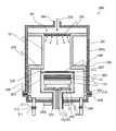
図1は、本実施の形態1における成膜装置の模式的な断面図である。Embodiment 1 FIG.
FIG. 1 is a schematic cross-sectional view of the film forming apparatus according to the first embodiment.
図1の成膜装置200において、201は成膜室としてのチャンバ、202はチャンバ内壁を被覆して保護する中空筒状のライナ、203a、203bはチャンバを冷却する冷却水の流路、204はプロセスガス225を導入する供給部、205は反応後のプロセスガスの排気部、206は気相成長を行うウェハなどの半導体基板、207は半導体基板206を支持するサセプタ、208は図示しない支持部に支持されて半導体基板206を加熱するヒータ、209はチャンバ201の上下部を連結するフランジ部、210はフランジ部209をシールするパッキン、211は排気部205と配管を連結するフランジ部、212はフランジ部211をシールするパッキンである。 In the
ライナ202は、透明性を備えた石英製である。ライナ202の頭部231の上部開口部には、半導体基板206の表面に対してプロセスガス225を均一に供給するためのガス整流板であるシャワープレート220が取り付けられている。 The
チャンバ201の底部には、チャンバ201の内部まで伸びる回転軸222が設けられている。回転軸222の上端には回転筒223が配設され、この回転筒223にサセプタ207が取り付けられている。これにより、サセプタ207は、回転筒223を介して回転し、さらに半導体基板206は、サセプタ207を介して回転する。この方法によれば、均一に加熱された半導体基板206の表面に新たなプロセスガスが次々に接触するので成膜速度の向上が図れる。
尚、回転筒223の内部には、後述するように、ヒータ208、リフレクタ101および断熱部102などが配置されるが、半導体基板206の温度を、例えば、1200℃や1600℃以上の高温に維持し、サセプタ207を900rpm以上の高速で回転することができるように、そうしたヒータ208などは、サセプタ207や回転筒223などの回転する部材とは離れて固定されている。A
As will be described later, the
チャンバ201の上部には、プロセスガス225を供給するための供給部204が設けられている。ガス供給部204から供給されたプロセスガス225は、シャワープレート220を通ってライナ202の内部に導入される。ここで、シャワープレート220に設けられた貫通孔221は、半導体基板206の置かれる位置に対応して設けられる。これにより、供給部204から供給されるプロセスガス225をサセプタ207上の半導体基板206の上に均一に供給することができる。 A
中空筒状の形状を有するライナ202は、シャワープレート220を支持する頭部231の内径がサセプタ207の配置された胴部230より小さくなるよう構成されている。すなわち、ライナ202の形状は、半導体基板206が配置される胴部230の内径に対して、プロセスガス225の流路となる頭部231の内径の方が小さくなっている。つまり、ライナ202は、胴部230に対して頭部231の断面積が絞られた構造を有している。 The
上記構造とすることで、シャワープレート220の貫通孔221から導入されたプロセスガス225が無駄に拡散する空間を小さくして、半導体基板206の表面に効率よく供給されるようにすることができる。 With the above structure, a space in which the
供給部204からチャンバ201内に供給されたプロセスガス225は、頭部231を通過して半導体基板206の表面に向かって効率よく流下する。このとき、半導体基板206表面でのプロセスガス225の流れをより均一にするよう、半導体基板206の周縁部分とライナ202との間の隙間は狭くなっていることが好ましい。具体的には、ライナ202の頭部231と胴部230との境にある、段部232の角部234と半導体基板206の周縁部分との間の隙間が狭くなっていることが好ましい。 The
回転筒223の内部には、(本発明における第1のヒータである)ヒータ208が配置されている。ヒータ208としては、SiC材料を用いて構成された抵抗加熱用のヒータが用いられる。このヒータは、発熱体としてSiC焼結体を用いたSiCヒータである。SiC焼結体は、粒界に不純物の少ない微細で均一な組織を有しており、高い導電性を備える。尚、耐熱性の観点ではSiCよりC(カーボン)の方が良好であるが、不純物などがエピタキシャル膜へ及ぼす影響を考慮するとSiCを用いることが好ましい。 A heater 208 (which is the first heater in the present invention) is disposed inside the
ヒータ208は、通電により発熱する発熱体、すなわち、SiC焼結体を有している。このSiC焼結体には、SiCコートがされている。かかるSiCコートは、温度を変えて順次成膜された複数のSiC膜からなる。 The
SiC焼結体は、SiC粉末を焼結して得られる。この場合、例えば、平均粒径の異なる複数のSiC粉末を混合し、これを焼結して、SiC焼結体とすることができる。各SiCの平均粒径とこれらの混合比率を選択することで、所望の電気比抵抗を示すSiCを得ることが可能である。混合物は所望の形状に成形された後に所定の温度で焼結される。尚、焼結方法および焼結時の雰囲気はいずれも制限されない。 The SiC sintered body is obtained by sintering SiC powder. In this case, for example, a plurality of SiC powders having different average particle sizes can be mixed and sintered to form a SiC sintered body. By selecting the average particle diameter of each SiC and the mixing ratio thereof, it is possible to obtain SiC exhibiting a desired electrical specific resistance. The mixture is formed into a desired shape and then sintered at a predetermined temperature. Note that the sintering method and the atmosphere during sintering are not limited.
尚、ヒータ208の形状は図1の構造に限定されるものではない。また、インヒータとアウトヒータの2種類のヒータによって半導体基板206を加熱する構成としてもよい。この場合、アウトヒータは、サセプタ207の周縁部を主に加熱するようにし、インヒータは、アウトヒータの下部に配置されて、サセプタ207の周縁部以外を主に加熱するようにすることができる。このようにすることにより、半導体基板206をより均一に加熱することができるので、半導体基板206の温度分布の均一性が向上する。 The shape of the
ヒータ208は、アーム形状をした導電性のブースバー(「第1の支持部」とも称する。)103によって支持されている。ブースバー103は、例えば、C(カーボン)をSiCで被覆してなる部材によって構成される。また、ブースバー103は、ヒータ208を支持する側とは反対の側で、石英製のヒータベース(「第2の支持部」とも称する。)104によって支持されている。そして、Mo(モリブデン)などの金属からなる導電性の連結部105によって、ブースバー103と電極棒(単に「電極」とも称する。)106が連結されることにより、電極棒106からヒータ208への給電が行われる。具体的には、電極棒106からヒータ208の発熱体に通電がされて発熱体が昇温する。 The
ヒータ208による加熱で変化する半導体基板206の表面温度は、放射温度計によって計測することができる。放射温度計は、例えば、チャンバ201の上部に設けることができる。この際、シャワープレート220を透明石英製とすれば、放射温度計による温度測定がシャワープレート220で妨げられないようにすることができる。計測した温度データは、図示しない制御機構に送られた後、ヒータ208の出力制御にフィードバックされる。これにより、半導体基板206を所望の温度となるように加熱することができる。 The surface temperature of the
回転筒223の内部において、ヒータ208の下方には、(本発明における第1のリフレクタである)リフレクタ(反射板)101が配置されている。リフレクタ101を設けることにより、ヒータ208からの熱がリフレクタ101で反射されて、サセプタ207上に載置された半導体基板206への加熱効率が向上する。リフレクタ101は、カーボンなどの熱伝導度の大きく耐熱性の高い材料で構成され、ヒータ208の近傍に配置されることが好ましい。そして、リフレクタ101の構成に好適な材料としては、C(カーボン)の他に、例えば、SiC(炭化珪素)、TaC(炭化タンタル)、W(タングステン)、Mo(モリブデン)などの1700℃以上の耐熱性がある材料を挙げることができる。 Inside the
リフレクタ101は、1枚の薄板からなるものとすることができるが、上記効果を得るには、複数枚の薄板を適当な間隔で離間させた構造とすることが好ましい。図1の例では、2枚の薄板を離間させて構成しているが、3枚以上の薄板を離間させてもよい。加熱効率を向上させる点から、本実施の形態では、5枚の薄板を離間させる構造とすることが特に好ましい。 The
成膜装置200においてヒータ208を動作させると、ヒータ208からの輻射熱によって、ヒータ208の周辺部材、すなわち、ブースバー103、ヒータベース104、連結部105および電極棒106などの温度も上昇する。このうち、ヒータベース104はSiO2(石英)によって構成されており、連結部105と電極棒106はMo(モリブデン)などの金属によって構成されている。これらの耐熱温度は、ヒータ208の構成部材であるSiCに比べて低い。このため、ヒータ208からの輻射熱によってこれらの周辺部材が劣化するおそれがある。When the
例えば、Si膜のエピタキシャル成長の場合、ウェハの温度は1200℃程度まで加熱される。SiC膜のエピタキシャル成長では、ウェハの温度は、1650℃〜1750℃まで加熱される。一方、石英の軟化点は1100℃程度であるので、このような高温下でエピタキシャル成長を行う場合には、ヒータベース104が劣化するおそれがある。 For example, in the case of epitaxial growth of a Si film, the wafer temperature is heated to about 1200 ° C. In the epitaxial growth of the SiC film, the temperature of the wafer is heated to 1650 ° C. to 1750 ° C. On the other hand, since the softening point of quartz is about 1100 ° C., the
周辺部材の劣化は、リフレクタ101を設けることである程度軽減することができる。すなわち、リフレクタ101によって、ヒータ208からの熱が半導体基板206の方へ反射されるので、周辺部材の劣化防止に効果がある。しかしながら、Si膜やSiC膜などの高温での加熱が必要な成膜工程の場合、リフレクタ101の設置のみでは周辺部材の劣化を十分に防ぐことができない。 Deterioration of the peripheral members can be reduced to some extent by providing the
そこで、本実施の形態では、リフレクタ101と、(本発明における第1の断熱部である)断熱部102とを組み合わせて用いる。具体的には、ヒータ208の下方にリフレクタ101を配置し、さらに、リフレクタ101の下方に断熱部102を配置する。断熱部102は、例えば、カーボン繊維を用いて構成されたものとすることができる。より具体的には、カーボン繊維に樹脂を染み込ませて加熱した形成された成形断熱材などとすることができる。断熱部102の配置により、ヒータ208からの輻射熱が断熱部102に吸収され、ヒータ208の周囲における過度の温度上昇を抑制することができる。したがって、ヒータ208の周辺部材の熱劣化を防ぐことができる。例えば、半導体基板206の温度が1650℃であるとき、本実施の形態の構成によれば、ヒータベース104の温度を1000℃程度にすることができる。これはSiO2(石英)の軟化点より低い温度であり、ヒータベース104の熱による変形などを引き起こさずに済む。Therefore, in the present embodiment, the
断熱部102は、蓄積した熱を逃がし難い特性を有するので、回転筒223内で半導体基板206からできるだけ離して配置する。本実施の形態の構成では、リフレクタ101の下方であって、リフレクタ101からできるだけ離れた位置に設ける。このようにすることにより、半導体基板206の温度制御への影響を最小限にして、ヒータ208の周辺部材の熱劣化を防ぐことが可能となる。 Since the
あるいは、断熱部102を鉛直方向に移動可能な構成としてもよい。例えば、エピタキシャル膜を形成するために、半導体基板206の温度を上昇させる際には、断熱部102が上方、すなわち、半導体基板206から近い位置にあるようにする。一方、エピタキシャル反応を終えて、半導体基板206をチャンバ201から搬出するため、半導体基板206の温度を降下させる際には、図2に示すように、断熱部102を下降させて半導体基板206から離れた位置に断熱部102があるようにする。尚、図2において、図1と同じ符号を付した部分は同じものであることを示している。 Or it is good also as a structure which can move the
本実施の形態においては、例えば、ヒータ208とリフレクタ101との距離を5mmとすることができる。リフレクタ101を5枚の薄板によって構成する場合、例えば、薄板1枚の厚みを2mmとすることができ、薄板間の距離を3.5mmとすることができる。また、例えば、リフレクタ101と断熱部102との距離を3.5mmとすることができ、断熱部102の厚みを25mmとすることができる。さらに、断熱部102の下方、ブースバー103までの距離は80mm程度とすることができる。 In the present embodiment, for example, the distance between the
断熱部102による微妙な温度調整を可能とするため、鉛直方向に沿って複数の断熱部102を設けることも可能である。例えば、2つまたは3つの断熱部102を使用し、これらの間に所定の隙間を設けて、2層または3層の断熱部とすることができる。 In order to enable delicate temperature adjustment by the
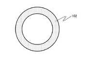
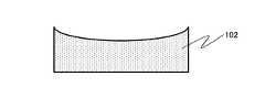
断熱部102の形状は、例えば、図3に示すようなドーナツ状とすることができる。また、図4に示すように、平面では円板状であるが、断面では、中央部の厚みが小さく、周辺部の厚みが大きい形状とすることもできる。図3や図4の構造とすることで、断熱部102による半導体基板206への影響を小さくしつつ、ヒータ208の周辺部材の熱劣化を防ぐことができる。 The shape of the
次に、実施の形態1の成膜方法について説明する。 Next, the film forming method of Embodiment 1 will be described.
図1の成膜装置200では、チャンバ201内でサセプタ207により半導体基板206が支持される。そして、回転軸222によって半導体基板206をサセプタ207を介して回転させながら、ヒータ208を用いて半導体基板206を1000℃以上に加熱する。この状態でチャンバ201内に反応ガスを含むプロセスガス225を、供給部204からシャワープレート220の貫通孔221を介して供給する。 In the
すると、半導体基板206の表面で熱分解反応または水素還元反応が起こり、半導体基板206の表面にエピタキシャル膜が形成される。その際、気相成長反応で消費されなかったプロセスガスの一部は、変性されたガスとなる。この変性ガスは、プロセスガス225とともに、チャンバ201の下部に設けられた排気部205から逐次排気される。 Then, a thermal decomposition reaction or a hydrogen reduction reaction occurs on the surface of the
一例として、Siエピタキシャル膜の成膜方法について述べる。 As an example, a method for forming a Si epitaxial film will be described.
まず、チャンバ201内に半導体基板206を搬送し、サセプタ207の上に載置する。半導体基板206としては、例えば、SiCウェハまたはSiウェハを用いることができる。あるいは、SiO2(石英)ウェハなどの他の絶縁性基板や、GaAs(ガリウム砒素)ウェハなどの高抵抗の半絶縁性基板などを用いることも可能である。First, the
次に、半導体基板206の上にSi膜を形成する。 Next, a Si film is formed on the
例えば、半導体基板206としてSiウェハを用い、これをサセプタ207の上に載置する。断熱部102が鉛直方向に移動可能な構造である場合には、上方、すなわち、半導体基板206の近くに位置するようにする。 For example, a Si wafer is used as the
次いで、常圧下または適当な減圧下で水素ガスを流しながら、サセプタ207に付随させて、Siウェハを50rpm程度で回転させる。 Next, the Si wafer is rotated at about 50 rpm in association with the
次に、ヒータ208によってSiウェハを1100℃〜1200℃に加熱する。断熱部102があることにより、ヒータ208の熱が断熱部102に蓄積されるので、Siウェハが効率よく加熱される。 Next, the Si wafer is heated to 1100 ° C. to 1200 ° C. by the
放射温度計(図示せず)による測定でSiウェハの温度が1150℃に達したことを確認した後は、徐々にSiウェハの回転数を上げていく。そして、供給部204からシャワープレート220を介して反応ガスをチャンバ201の内部に供給する。 After confirming that the temperature of the Si wafer has reached 1150 ° C. by measurement with a radiation thermometer (not shown), the rotational speed of the Si wafer is gradually increased. Then, the reaction gas is supplied into the
反応ガスとしては、SiHCl3(トリクロロシラン)を用いることができ、キャリアガスとしての水素ガスと混合した状態で、供給部204からチャンバ201の内部に導入する。チャンバ201の内部に導入された反応ガスは、Siウェハの方に流下する。そして、Siウェハの温度を1150℃に維持し、サセプタ207を900rpm以上の高速で回転させながら、供給部204からシャワープレート220を介して次々に新たな反応ガスをSiウェハに供給する。As the reaction gas, SiHCl3 (trichlorosilane) can be used, and is introduced into the
以上のようにして、Siウェハの上に均一な厚さのSiエピタキシャル膜を成長させることができる。 As described above, a Si epitaxial film having a uniform thickness can be grown on a Si wafer.
上記の通り、Siエピタキシャル成長工程において、半導体基板206を加熱するためにヒータ208を用いると、ヒータ208からの輻射熱は、半導体基板206だけでなく、他の部材にも伝わってそれらを昇温させてしまう。こうしたことは、ヒータ208の近傍に位置する部材、例えば、ブースバー103、ヒータベース104、連結部105および電極棒106などにおいて顕著である。ヒータ208からの輻射熱によって、周辺部材の温度がそれらの軟化点以上になると、周辺部材に変形などが起こる。 As described above, when the
そこで、ヒータ208の下方に、リフレクタ101を配置し、さらにリフレクタ101の下方に断熱部102を配置する。すると、リフレクタ101によって、ヒータ208からの熱が半導体基板206の方へ反射される。また、断熱部102によって、ヒータ208からの熱が吸収される。したがって、この構成によれば、ヒータ208の周囲における過度の温度上昇を抑制して、ヒータ208の周辺部材の熱劣化を防ぐことができる。 Therefore, the
半導体基板206の上に、所定の膜厚のSi膜を形成した後は、プロセスガス225の供給を終了する。そして、半導体基板206が所定の温度まで冷却されたのを確認してから、チャンバ201の外部に半導体基板206を搬出する。断熱部102が鉛直方向に移動可能な構造である場合には、断熱部102を下降させて半導体基板206から離れた位置にあるようにすることで、半導体基板206の冷却を早めることができる。 After the Si film having a predetermined thickness is formed on the
他の例として、SiCエピタキシャル膜の成膜方法について述べる。 As another example, a method for forming a SiC epitaxial film will be described.
まず、サセプタ207上に半導体基板206を載置し、半導体基板206を加熱するとともに、サセプタ207を介して半導体基板206を回転させる。この状態で半導体基板206の表面に反応ガスを接触させることで、半導体基板206の表面にSiCエピタキシャル膜を形成する。 First, the
半導体基板206としては、例えば、SiCウェハまたはSiウェハを用いることができる。あるいは、SiO2(石英)ウェハなどの他の絶縁性基板や、GaAs(ガリウム砒素)ウェハなどの高抵抗の半絶縁性基板などを用いることも可能である。As the
具体的には、まず、半導体基板206をチャンバ201内に搬送する。次に、サセプタ207に付随させて、サセプタ207上に載置された半導体基板206を50rpm程度で回転させる。 Specifically, first, the
ヒータ208に電流を供給して作動させ、ヒータ208から発せられる熱によって半導体基板206を加熱する。半導体基板206の温度が、成膜温度である1500℃〜1700℃までの間の所定の温度、例えば、1650℃に達するまで徐々に加熱する。このとき、チャンバ201の壁部分に設けた流路203a、203bに冷却水を流すことで、過度にチャンバ201が昇温するのを防止することができる。 An electric current is supplied to the
半導体基板206の温度が1650℃に達した後は、ヒータ208により1650℃近辺での緻密な温度調整がなされる。このとき、半導体基板206の温度は、放射温度計(図示せず)を用いて測定することができる。 After the temperature of the
放射温度計による測定で半導体基板206の温度が所定温度に達したことを確認した後は、徐々に半導体基板206の回転数を上げていく。例えば、900rpm程度の回転数とするのがよい。 After confirming that the temperature of the
また、供給部204から反応ガスを含むプロセスガス225を供給し、シャワープレート220を介して、プロセスガス225を半導体基板206の上に流下させる。このとき、プロセスガス225は、整流板であるシャワープレート220を通過して整流され、下方の半導体基板206に向かってほぼ鉛直に流下して、いわゆる縦フローを形成する。 Further, the
プロセスガス225としては、例えば、SiH4(モノシラン)およびC3H8(プロパン)を用いることができ、キャリアガスとしての水素ガスと混合した状態で、ガス供給部204からチャンバ201の内部に導入する。尚、SiH4に代えて、Si2H6(ジシラン)、SiH3Cl(モノクロロシラン)、SiH2Cl2(ジクロロシラン)、SiHCl3(トリクロロシラン)、SiCl4(テトラクロロシラン)などを用いてもよい。As the
尚、チャンバ201の上部には、供給部204とは別に、キャリアガスである水素ガスをチャンバ201内に供給するための水素ガス供給部をさらに設けることも可能である。その場合、供給部204からC(カーボン)のソースガスを含むガス、例えばC2H2(アセチレン)を供給し、水素ガス供給部からキャリアガスである水素ガスを供給し、チャンバ201内で混合して半導体基板206の表面に供給する。Note that a hydrogen gas supply unit for supplying hydrogen gas as a carrier gas into the
半導体基板206の表面に到達したプロセスガス225は、熱分解反応または水素還元反応を起こす。これにより、半導体基板206の表面にSiC膜が形成される。プロセスガス225の内で気相成長反応に使用されたもの以外のガスは、変性されたガスとなり、チャンバ201の下部に設けられた排気部205から逐次排気される。 The
SiCをエピタキシャル成長させるには、半導体基板206を1500℃以上の温度まで昇温する必要がある。このため、サセプタ207には高耐熱性の材料を用いる必要があり、具体的には、等方性黒鉛の表面にCVD(Chemical Vapor Deposition)法によってSiCを被覆したものなどが用いられる。サセプタ207の形状は、半導体基板206を載置可能な形状であれば特に限定されるものではなく、リング状や円盤状など適宜選択して用いられる。 In order to epitaxially grow SiC, it is necessary to raise the temperature of the
上記の通り、SiCエピタキシャル成長工程では、半導体基板206を非常に高温にする必要がある。しかし、半導体基板206を高温の状態にするためにヒータ208で加熱すると、ヒータ208からの輻射熱は、半導体基板206だけでなく、他の部材にも伝わってそれらを昇温させてしまう。こうしたことは、ヒータ208の近傍に位置する部材、例えば、ブースバー103、ヒータベース104、連結部105および電極棒106などにおいて顕著である。ヒータ208からの輻射熱によって、周辺部材の温度がそれらの軟化点以上になると、周辺部材に変形などが起こる。 As described above, in the SiC epitaxial growth process, the
そこで、ヒータ208の下方に、リフレクタ101を配置し、さらにリフレクタ101の下方に断熱部102を配置する。すると、リフレクタ101によって、ヒータ208からの熱が半導体基板206の方へ反射される。また、断熱部102によって、ヒータ208からの熱が吸収される。したがって、この構成によれば、ヒータ208の周囲における過度の温度上昇を抑制して、ヒータ208の周辺部材の熱劣化を防ぐことができる。 Therefore, the
半導体基板206の上に、所定の膜厚のSiC膜を形成した後は、プロセスガス225の供給を終了する。そして、半導体基板206が所定の温度まで冷却されたのを確認してから、チャンバ201の外部に半導体基板206を搬出する。 After the SiC film having a predetermined film thickness is formed on the
本実施の形態の成膜方法によれば、リフレクタと断熱部を組み合わせてヒータの下方に配置し、基板を加熱するので、ヒータからの輻射熱による周辺部材の劣化を防ぎながら、高温下でのエピタキシャル成長反応を行うことができる。かかる本実施の形態の成膜装置および成膜方法は、Siエピタキシャル膜やSiCエピタキシャル膜の成膜に適用可能であり、特に、SiCエピタキシャル膜などの高温下での成膜に好適である。 According to the film forming method of the present embodiment, the reflector and the heat insulating portion are combined and arranged below the heater to heat the substrate, so that epitaxial growth under high temperature is prevented while preventing deterioration of peripheral members due to radiant heat from the heater. The reaction can be performed. Such a film forming apparatus and film forming method of the present embodiment can be applied to the formation of a Si epitaxial film or a SiC epitaxial film, and is particularly suitable for forming a SiC epitaxial film or the like at a high temperature.
実施の形態2.
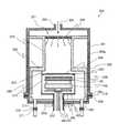
図5は、本実施の形態2における成膜装置の模式的な断面図である。尚、図5において、図1と同じ符号を付した部分は同じものであることを示している。Embodiment 2. FIG.
FIG. 5 is a schematic cross-sectional view of the film forming apparatus according to the second embodiment. In FIG. 5, the parts denoted by the same reference numerals as those in FIG. 1 are the same.
成膜装置300では、ライナ202の外周、より詳しくは、ライナ202の頭部231の外周に、(第2のヒータとしての)上部ヒータ35が配設されている。つまり、成膜装置300は、半導体基板206の下面側に配置され、半導体基板206を下面側から加熱するヒータ208と、ヒータ208の上方であって、ライナ202の周囲に設けられ、半導体基板206を上方から加熱する上部ヒータ35とを有する。この構成によれば、上部ヒータ35は、(第1のヒータである)ヒータ208の上方に配置される。 In the
上部ヒータ35は、複数の小ヒータによって構成され、各々が独立に制御可能な構造とすることができる。 The
図5では、上部ヒータ35は、鉛直方向に配列した3つの小ヒータ(第一加熱ヒータ36、第二加熱ヒータ37、第三加熱ヒータ38)によって構成される。これらの小ヒータは、何れもC(カーボン)などから製造された抵抗加熱型ヒータとすることができる。 In FIG. 5, the
小ヒータは、ライナ202の胴部230に近い側から、シャワープレート220が配設された上部開口部側に向け順次配置されている。これらは、例えば、ねじ止めなどの手段により、第一ヒータ接続部39、第二ヒータ接続部40および第三ヒータ接続部41に接続し、これらの接続部によって支持されている。さらに、第一ヒータ接続部39、第二ヒータ接続部40および第三ヒータ接続部41は、それぞれチャンバ201の側壁を貫通し、制御部42を介して、図示しないヒータ電流供給部に接続している。このような構造によって、第一加熱ヒータ36、第二加熱ヒータ37および第三加熱ヒータ38には、対応する第一ヒータ接続部39、第二ヒータ接続部40および第三ヒータ接続部41を介し、それぞれ独立にヒータ電流の供給が行われる。制御部42は、第一加熱ヒータ36、第二加熱ヒータ37、第三加熱ヒータ38のそれぞれに供給されるヒータ電流を制御することができ、これによって、各加熱ヒータの加熱温度を調整することができる。 The small heaters are sequentially arranged from the side closer to the
小ヒータの中で最下部に位置する第一加熱ヒータ36は、図5に示すように、ライナ202の形状に対応した形状を有する。すなわち、第一加熱ヒータ36は、ライナ202の頭部231と胴部230の境部分の形状に対応するよう、下部側が屈曲する構造を有する。これにより、半導体基板206に対する効率的な加熱が可能となる。 As shown in FIG. 5, the
尚、成膜装置300において、上部ヒータ35を構成する小ヒータは3つに限られるものではなく、2つあるいは4つ以上とすることもできる。また、上部ヒータ35を、小ヒータが組み合わされた構造ではなく、1つのヒータによって構成された構造とすることも可能である。 In the
図5において、成膜装置300は、チャンバ201の側壁部分とライナ202の頭部231の間に、(第2のリフレクタとしての)リフレクタ45を有する。このリフレクタ45は、上部ヒータ35を構成する、第一加熱ヒータ36、第二加熱ヒータ37および第三加熱ヒータ38を包囲するように配設されている。リフレクタ45を設けることにより、上部ヒータ35からの熱がリフレクタ45で反射されて、半導体基板206への加熱効率が向上する。また、リフレクタ45の設置により、上部ヒータ35からの熱がチャンバ201の側壁に届いて、チャンバ201が過度に昇温するのを防ぐこともできる。 In FIG. 5, the
リフレクタ45は、耐熱性が高く熱伝導度の高いC(カーボン)を用いて構成される。尚、リフレクタ45の構成に好適な材料としては、C(カーボン)の他に、例えば、SiC(炭化珪素)、TaC(炭化タンタル)、W(タングステン)、Mo(モリブデン)などの1700℃以上の耐熱性がある材料を挙げることができる。図5の例では、リフレクタ45は、ライナ202の胴部230と頭部231の境に位置する、胴部230の天井部分に立設されている。また、図5では、リフレクタ45は、上部ヒータ35から発せられる熱を効率よく半導体基板206の側に反射するよう、3層構造となっている。尚、リフレクタ45を単層構造とすることや、2層構造または4層以上の構造とすることも、熱の反射性能や遮蔽性能を考慮して当然に可能である。 The
本実施の形態では、上部ヒータ35の設置位置に、チャンバ201の内壁をカバーするように、(第2の断熱部としての)断熱部46を配設する。断熱部46を設けることで、上部ヒータ35からの熱が断熱部46によって遮断され、ステンレスなどからなるチャンバ201の側壁部分が上部ヒータ35からの熱によって過剰に昇温することを防止することができる。 In the present embodiment, the heat insulating portion 46 (as the second heat insulating portion) is disposed at the installation position of the
また、本実施の形態の成膜装置300では、実施の形態1の成膜装置200と同様に、第1のヒータとしてのヒータ208の下方に、第1のリフレクタとしてのリフレクタ101を配置し、さらにリフレクタ101の下方に、第1の断熱部としての断熱部102を配置する。すると、リフレクタ101によって、ヒータ208からの熱が半導体基板206の方へ反射される。また、断熱部102によって、ヒータ208からの熱が吸収される。したがって、この構成によれば、ヒータ208の周囲における過度の温度上昇を抑制して、ヒータ208の周辺部材の熱劣化を防ぐことができる。 Further, in the
以上述べたように、本実施の形態によれば、リフレクタ101と断熱部102を組み合わせてヒータ208の下方に配置することにより、ヒータ208からの輻射熱による周辺部材の劣化を防ぐことができる。また、半導体基板206をその上方から加熱する上部ヒータ35を設けることにより、ヒータ208と相まって、半導体基板206を効率的に加熱することができる。さらに、リフレクタ45や断熱部46を設けることで、上部ヒータ35からの熱がチャンバ201の側壁に届いて、チャンバ201が過度に昇温するのを防ぐこともできる。 As described above, according to the present embodiment, the
尚、本実施の形態においては、上部ヒータ35の周囲にリフレクタ45や断熱部46がなくてもよく、あるいは、上部ヒータ35の周囲にリフレクタ45だけが設けられていてもよい。 In the present embodiment, the
次に、実施の形態2の成膜方法について説明する。 Next, the film forming method of Embodiment 2 will be described.
本実施の形態の成膜装置300は、実施の形態1と同様に、Siエピタキシャル膜やSiCエピタキシャル膜の成膜に適用可能である。そして、特に、SiCエピタキシャル膜などの成膜のように、均一な基板温度を維持しながら非常に高い温度で成膜する場合に好適である。 The
成膜装置300を用いたSiCエピタキシャル膜の形成は、以下のようにして行うことができる。 The formation of the SiC epitaxial film using the
まず、半導体基板206であるSiCウェハをチャンバ201の内部に搬入する。次いで、サセプタ207の上に半導体基板206を載置する。このとき、断熱部102が鉛直方向に移動可能な構造である場合には、上方、すなわち、半導体基板206の近くに位置するようにする。 First, an SiC wafer as the
次いで、常圧下または適当な減圧下で水素ガスを流しながら、サセプタ207に付随させて、半導体基板206を50rpm程度で回転させる。 Next, the
次に、ヒータ208と上部ヒータ35によって半導体基板206を加熱する。このとき、上部ヒータ35を構成する複数の小ヒータについて各々温度調整をしながら加熱する。具体的には、電極棒106から連結部105とブースバー103を介してヒータ208に給電が行われ、ヒータ208の発熱体が昇温する。また、上部ヒータ35を構成する、第一加熱ヒータ36、第二加熱ヒータ37および第三加熱ヒータ38のそれぞれに、第一ヒータ接続部39、第二ヒータ接続部40および第三ヒータ接続部41を介して独立に電流が供給され、各小ヒータの発熱体が昇温する。 Next, the
本実施の形態では、ヒータ208の下方にリフレクタ101が配置され、さらに、リフレクタ101の下方に断熱部102が配置されていることにより、リフレクタ101によって、ヒータ208からの熱が半導体基板206の方へ反射される。また、断熱部102によって、ヒータ208からの輻射熱が断熱部102に吸収される。したがって、ヒータ208の周囲における過度の温度上昇を抑制し、ヒータ208の周辺部材の熱劣化を防ぐことができる。 In the present embodiment, the
また、成膜装置300では、ライナ202の頭部231の外周に上部ヒータ35が配設されていることによって、ヒータ208と相まって半導体基板206を効率よく高温にすることができる。さらに、上部ヒータ35を複数の小ヒータによって構成し、各々が独立に制御可能な構造とすることで、半導体基板206の温度を細かく調整して均一な温度分布を実現することが可能である。 In the
さらに、成膜装置300は、チャンバ201の側壁部分とライナ202の頭部231の間にリフレクタ45を有する。また、上部ヒータ35の設置位置に、チャンバ201の内壁をカバーするように断熱部46が配設されている。リフレクタ45を設けることにより、上部ヒータ35からの熱がリフレクタ45で反射されて、半導体基板206への加熱効率が向上する。また、リフレクタ45の設置により、上部ヒータ35からの熱がチャンバ201の側壁に届いて、チャンバ201が過度に昇温するのを防ぐこともできる。さらに、断熱部46を設けることで、上部ヒータ35からの熱が断熱部46によって遮断されるので、チャンバ201の側壁部分の温度上昇をより効果的に抑制することができる。 Further, the
ヒータ208と上部ヒータ35は協同して、半導体基板206の温度が、成膜温度である1500℃〜1700℃範囲の所定の温度、例えば、1650℃に達するまで加熱する。このとき、チャンバ201の壁部分に設けた流路203a、203bに冷却水を流すことで、過度にチャンバ201が昇温するのを防止することができる。 The
1650℃に達した後は、この温度付近における緻密な温度調整をヒータ208によって行うことができる。一方、上部ヒータ35は、ヒータ208による温度調整を助けるように作用する。例えば、半導体基板206を1650℃に維持しようとする場合、上部ヒータ35を構成する、第一加熱ヒータ36、第二加熱ヒータ37および第三加熱ヒータ38の温度をそれぞれ1700℃〜1800℃の範囲に調整することで、ヒータ208の温度を1800℃以下とすることができる。つまり、上部ヒータ35がヒータ208の補助的役割を担うことで、ヒータ208の過度の温度上昇を抑制することができる。したがって、上部ヒータ35の設置は、ヒータ208の周囲の過度の温度上昇を抑制し、ヒータ208の周辺部材の熱劣化を防ぐ点からも有効である。 After reaching 1650 ° C., precise temperature adjustment near this temperature can be performed by the
放射温度計(図示せず)による測定で、半導体基板206の温度が所定温度に達したことを確認した後は、徐々に半導体基板206の回転数を上げていく。例えば、900rpm程度の回転数まで上昇させる。そして、供給部204からプロセスガス225をチャンバ201内に供給する。プロセスガス225としては、例えば、SiH4(モノシラン)およびC3H8(プロパン)を用いることができ、キャリアガスとしての水素ガスと混合した状態で、ガス供給部204からチャンバ201の内部に導入する。尚、SiH4に代えて、Si2H6(ジシラン)、SiH3Cl(モノクロロシラン)、SiH2Cl2(ジクロロシラン)、SiHCl3(トリクロロシラン)、SiCl4(テトラクロロシラン)などを用いてもよい。After confirming that the temperature of the
チャンバ201内に導入されたプロセスガス225は、チャンバ201内に設けられたライナ202の頭部231に取り付けられたシャワープレート220を通過する。多数の貫通孔221を有するシャワープレート220は、ガス整流板として作用する。プロセスガス225は、シャワープレート220の貫通孔を通過することで、均一な流れとなって半導体基板206の方へ流下し、半導体基板206の表面にSiC膜が形成される。 The
半導体基板206の上に所定の膜厚のSiC膜を形成した後は、プロセスガス225の供給を終了する。ここで、プロセスガス225とともにキャリアガスの供給も終了することができるが、プロセスガス225の供給のみを終了した後、放射温度計で半導体基板206が所定の温度より低くなったのを確認してから、キャリアガスの供給を終了するようにしてもよい。 After the SiC film having a predetermined thickness is formed on the
半導体基板206が所定の温度まで冷却された後は、チャンバ201の外部に半導体基板206を搬出する。断熱部102が鉛直方向に移動可能な構造である場合には、断熱部102を下降させて半導体基板206から離れた位置にあるようにすることで、半導体基板206の冷却を早めることができる。 After the
本実施の形態の成膜方法によれば、第1のリフレクタと第1の断熱部を組み合わせて第1のヒータの下方に配置し、基板を加熱するので、第1のヒータからの輻射熱による周辺部材の劣化を防ぎながら、高温下でのエピタキシャル成長反応を行うことができる。また、基板の上方に設けた第2のヒータによっても基板を加熱するので、第1のヒータと相まって基板を効率的に加熱することができると同時に、第1のヒータの過度の温度上昇を防いで、第1のヒータの周辺部材への影響をより低減することができる。またに、第2のヒータの周囲に第2のリフレクタを配置することにより、第2のヒータからの熱が成膜室の側壁に届いて、成膜室が過度に昇温するのを防ぐことができる。さらに、第2のリフレクタの周囲に第2の断熱部を配置することにより、第2のヒータからの熱が第2の断熱部によって遮断されるので、成膜室の側壁部分の温度上昇をより効果的に抑制することができる。 According to the film forming method of the present embodiment, the first reflector and the first heat insulating portion are combined and disposed below the first heater to heat the substrate, so that the periphery due to the radiant heat from the first heater An epitaxial growth reaction can be performed at a high temperature while preventing deterioration of the member. Further, since the substrate is also heated by the second heater provided above the substrate, the substrate can be efficiently heated in combination with the first heater, and at the same time, an excessive temperature rise of the first heater is prevented. Thus, the influence on the peripheral members of the first heater can be further reduced. In addition, by disposing the second reflector around the second heater, it is possible to prevent heat from the second heater from reaching the side wall of the film formation chamber and excessively increasing the temperature of the film formation chamber. Can do. Further, by arranging the second heat insulating portion around the second reflector, the heat from the second heater is blocked by the second heat insulating portion, so that the temperature rise of the side wall portion of the film forming chamber is further increased. It can be effectively suppressed.
本発明の特徴と利点は、次のようにまとめられる。 The features and advantages of the present invention can be summarized as follows.
本発明の成膜装置によれば、ヒータの輻射熱による周辺部材の劣化を抑制することができる。 According to the film forming apparatus of the present invention, it is possible to suppress the deterioration of the peripheral members due to the radiant heat of the heater.
本発明の成膜方法によれば、ヒータの輻射熱による周辺部材の劣化を抑制しつつ、成膜を行うことができる。 According to the film forming method of the present invention, film formation can be performed while suppressing deterioration of peripheral members due to the radiant heat of the heater.
尚、本発明は上記各実施の形態に限定されるものではなく、本発明の趣旨を逸脱しない範囲内で種々変形して実施することができる。 The present invention is not limited to the above-described embodiments, and various modifications can be made without departing from the spirit of the present invention.
例えば、実施の形態1および2では、成膜室内に載置される基板を回転させながら成膜処理を行う例について述べたが、本発明はこれに限られるものではない。本発明の成膜装置は、基板を回転させないで成膜してもよい。 For example, in Embodiments 1 and 2, the example in which the film formation process is performed while rotating the substrate placed in the film formation chamber is described, but the present invention is not limited to this. The film forming apparatus of the present invention may form a film without rotating the substrate.
また、上記各実施の形態では、成膜装置の一例としてエピタキシャル成長装置を挙げたが、本発明はこれに限られるものではない。成膜室内に反応ガスを供給し、ウェハを加熱しながらその表面に膜を形成する成膜装置であれば、CVD(Chemical Vapor Deposition)装置などの他の成膜装置であってもよい。 In each of the above embodiments, an epitaxial growth apparatus is described as an example of a film forming apparatus, but the present invention is not limited to this. Any other film forming apparatus such as a CVD (Chemical Vapor Deposition) apparatus may be used as long as it supplies a reactive gas into the film forming chamber and forms a film on the surface while heating the wafer.
200、300 成膜装置
201 チャンバ
202 ライナ
203a、203b 流路
204 供給部
205 排気部
206 半導体基板
207 サセプタ
208 ヒータ
209、211 フランジ部
210、212 パッキン
220 シャワープレート
221 貫通孔
222 回転軸
223 回転筒
225 プロセスガス
230 胴部
231 頭部
232 段部
234 角部
45、101 リフレクタ
46、102 断熱部
103 ブースバー
104 ヒータベース
105 連結部
106 電極棒
35 上部ヒータ
36 第一加熱ヒータ
37 第二加熱ヒータ
38 第三加熱ヒータ
39 第一ヒータ接続部
40 第二ヒータ接続部
41 第三ヒータ接続部
42 制御部
200, 300
Claims (15)
Translated fromJapanese前記成膜室内に載置される基板を加熱する第1のヒータと、
前記第1のヒータの下方に配置される第1のリフレクタと、
前記第1のリフレクタの下方に配置される第1の断熱部とを有することを特徴とする成膜装置。A deposition chamber;
A first heater for heating a substrate placed in the film formation chamber;
A first reflector disposed below the first heater;
A film forming apparatus comprising: a first heat insulating portion disposed below the first reflector.
前記第1のヒータを支持する導電性の第1の支持部と、
前記第1の支持部を支持する第2の支持部と、
前記サセプタを上部で支持し、前記第1のヒータ、前記第1の支持部および前記第2の支持部を内部に配置する回転筒と、
前記成膜室の下部に配置されて前記回転筒を回転させる回転軸と、
前記回転軸の内部に設けられ、前記第1の支持部を介して前記第1のヒータに給電する電極と、
前記電極の上端部によって下方から貫通されてこれを固定するとともに、前記第1の支持部と前記第2の支持部を下方から支持する導電性の連結部とを有し、
前記第1のリフレクタと前記第1の断熱部は、前記回転筒の内部であって、前記第1のヒータと前記第2の支持部との間に配置されることを特徴とする請求項1〜3のいずれか1項に記載の成膜装置。A susceptor that supports a substrate placed in the film formation chamber;
A conductive first support portion for supporting the first heater;
A second support part for supporting the first support part;
A rotating cylinder that supports the susceptor at an upper portion and arranges the first heater, the first support portion, and the second support portion inside,
A rotating shaft disposed at a lower portion of the film forming chamber to rotate the rotating cylinder;
An electrode provided inside the rotating shaft and supplying power to the first heater via the first support;
The upper end portion of the electrode is penetrated from below to fix it, and has a first connecting portion and a conductive connecting portion for supporting the second supporting portion from below,
2. The first reflector and the first heat insulating part are disposed inside the rotating cylinder and are disposed between the first heater and the second support part. The film-forming apparatus of any one of -3.
前記電極と前記連結部は、いずれも金属で構成されることを特徴とする請求項4に記載の成膜装置。The second support portion is made of SiO2 (quartz),
The film forming apparatus according to claim 4, wherein both the electrode and the connecting portion are made of metal.
前記成膜室の内壁と前記ライナの間であって、前記第1のヒータの上方に設けられた第2のヒータとを有することを特徴とする請求項1〜5のいずれか1項に記載の成膜装置。A cylindrical liner covering the inner wall of the film forming chamber;
6. The apparatus according to claim 1, further comprising: a second heater provided between the inner wall of the film formation chamber and the liner and above the first heater. Film forming equipment.
前記小ヒータをそれぞれ独立に制御する制御部を有することを特徴とする請求項6に記載の成膜装置。The second heater is composed of a plurality of small heaters arranged in the vertical direction,
The film forming apparatus according to claim 6, further comprising a control unit that controls each of the small heaters independently.
前記回転軸の内部に電極を配置し、
前記回転筒の内部に、第1のヒータと、前記第1のヒータを支持する導電性の第1の支持部と、前記第1の支持部を支持する第2の支持部と、前記第1の支持部および前記第2の支持部を支持するとともに、前記電極と前記第1の支持部を給電可能に接続する導電性の連結部とを配置し、
前記第1のヒータの下方に第1のリフレクタを配置し、
前記第1のリフレクタの下方かつ前記第2の支持部の上方に第1の断熱部を配置して、
前記電極から前記第1のヒータへ給電して前記基板を加熱することを特徴とする成膜方法。The substrate is placed on a susceptor provided in a film formation chamber, the substrate is heated, and a rotating cylinder in which the susceptor is disposed on the upper part is rotated by a rotation shaft provided in a lower part of the film formation chamber, A film forming method for forming a film on a surface of the substrate by supplying a reaction gas into a film forming chamber,
An electrode is arranged inside the rotating shaft,
Inside the rotating cylinder, a first heater, a conductive first support part that supports the first heater, a second support part that supports the first support part, and the first And supporting the second support part and the second support part, and arranging the electrode and the conductive connecting part to connect the first support part so as to be able to supply power,
Disposing a first reflector below the first heater;
A first heat insulating part is disposed below the first reflector and above the second support part,
A film forming method, wherein the substrate is heated by supplying power from the electrode to the first heater.
The reaction gas is composed of SiH4 (monosilane), Si2 H6 (disilane), SiH3 Cl (monochlorosilane), SiH2 Cl2 (dichlorosilane), SiHCl3 (trichlorosilane), and SiCl4 (tetrachlorosilane). The film-forming method according to claim 12, comprising at least one of them.
Priority Applications (1)
| Application Number | Priority Date | Filing Date | Title |
|---|---|---|---|
| JP2012066938AJP5639104B2 (en) | 2011-03-24 | 2012-03-23 | Deposition equipment |
Applications Claiming Priority (5)
| Application Number | Priority Date | Filing Date | Title |
|---|---|---|---|
| JP2011066130 | 2011-03-24 | ||
| JP2011066130 | 2011-03-24 | ||
| JP2011253333 | 2011-11-18 | ||
| JP2011253333 | 2011-11-18 | ||
| JP2012066938AJP5639104B2 (en) | 2011-03-24 | 2012-03-23 | Deposition equipment |
Publications (2)
| Publication Number | Publication Date |
|---|---|
| JP2013128086Atrue JP2013128086A (en) | 2013-06-27 |
| JP5639104B2 JP5639104B2 (en) | 2014-12-10 |
Family
ID=46877689
Family Applications (1)
| Application Number | Title | Priority Date | Filing Date |
|---|---|---|---|
| JP2012066938AActiveJP5639104B2 (en) | 2011-03-24 | 2012-03-23 | Deposition equipment |
Country Status (3)
| Country | Link |
|---|---|
| US (1) | US20120244684A1 (en) |
| JP (1) | JP5639104B2 (en) |
| KR (1) | KR101349945B1 (en) |
Cited By (4)
| Publication number | Priority date | Publication date | Assignee | Title |
|---|---|---|---|---|
| JP2017183393A (en)* | 2016-03-29 | 2017-10-05 | 株式会社日立国際電気 | Substrate processing apparatus, manufacturing method of semiconductor device, and program |
| WO2019044440A1 (en)* | 2017-09-01 | 2019-03-07 | 株式会社ニューフレアテクノロジー | Vapor-phase growth device and vapor-phase growth method |
| WO2019044392A1 (en)* | 2017-08-30 | 2019-03-07 | 株式会社ニューフレアテクノロジー | Vapor-phase deposition method |
| TWI868678B (en)* | 2022-05-06 | 2025-01-01 | 日商紐富來科技股份有限公司 | Vapor phase growth apparatus |
Families Citing this family (20)
| Publication number | Priority date | Publication date | Assignee | Title |
|---|---|---|---|---|
| JP2010016225A (en)* | 2008-07-04 | 2010-01-21 | Tokyo Electron Ltd | Thermal control mechanism and semiconductor manufacturing device using the same |
| JP5732284B2 (en)* | 2010-08-27 | 2015-06-10 | 株式会社ニューフレアテクノロジー | Film forming apparatus and film forming method |
| JP5395102B2 (en)* | 2011-02-28 | 2014-01-22 | 株式会社豊田中央研究所 | Vapor growth equipment |
| GB201304631D0 (en)* | 2013-03-14 | 2013-05-01 | Malvern Instr Ltd | Monomer detection in protein separation |
| JP6026333B2 (en)* | 2013-03-25 | 2016-11-16 | 株式会社ニューフレアテクノロジー | Film forming apparatus and film forming method |
| GB201309583D0 (en)* | 2013-05-29 | 2013-07-10 | Spts Technologies Ltd | Apparatus for processing a semiconductor workpiece |
| KR102116508B1 (en)* | 2013-08-29 | 2020-05-28 | 에스케이실트론 주식회사 | Apparatus for manufacturing epitaxial wafer |
| US9837250B2 (en)* | 2013-08-30 | 2017-12-05 | Applied Materials, Inc. | Hot wall reactor with cooled vacuum containment |
| JP6158025B2 (en)* | 2013-10-02 | 2017-07-05 | 株式会社ニューフレアテクノロジー | Film forming apparatus and film forming method |
| KR101634581B1 (en)* | 2014-10-13 | 2016-06-29 | 한국생산기술연구원 | A reactor chamber for chemical vapor deposition |
| KR101691993B1 (en)* | 2015-08-11 | 2017-01-02 | 성균관대학교산학협력단 | Chamber for chemical vapor deposition device |
| US20180066381A1 (en)* | 2016-09-05 | 2018-03-08 | Nuflare Technology, Inc. | Vapor phase growth apparatus and vapor phase growth method |
| JP2020061388A (en)* | 2016-09-07 | 2020-04-16 | 株式会社Mirai | Manufacturing device for electronic apparatus, control method therefor, electronic apparatus, and manufacturing method thereof |
| JP2018101721A (en)* | 2016-12-21 | 2018-06-28 | 株式会社ニューフレアテクノロジー | Vapor growth method |
| CN214848503U (en) | 2018-08-29 | 2021-11-23 | 应用材料公司 | Injector apparatus, substrate processing apparatus, and structures implemented in machine-readable media |
| US20230060692A1 (en)* | 2021-08-30 | 2023-03-02 | Taiwan Semiconductor Manufacturing Company Ltd. | Annealing apparatus and method of operating the same |
| JP2024541233A (en)* | 2021-10-27 | 2024-11-08 | シランナ・ユー・ブイ・テクノロジーズ・プライベート・リミテッド | Method and system for heating a wide bandgap substrate - Patents.com |
| KR20240109261A (en) | 2021-11-10 | 2024-07-10 | 실라나 유브이 테크놀로지스 피티이 리미티드 | Ultra-widebandgap semiconductor device containing magnesium germanium oxide |
| EP4430671A4 (en) | 2021-11-10 | 2025-09-24 | Silanna UV Technologies Pte Ltd | Epitaxial oxide materials, structures and devices |
| CN116005255B (en)* | 2023-01-06 | 2025-06-17 | 宁波恒普技术股份有限公司 | Thermal field insulation component for film forming device and vertical film forming device |
Citations (5)
| Publication number | Priority date | Publication date | Assignee | Title |
|---|---|---|---|---|
| JPH04335520A (en)* | 1991-05-13 | 1992-11-24 | Fuji Electric Co Ltd | Vapor phase growth equipment |
| JPH0930893A (en)* | 1995-05-16 | 1997-02-04 | Hitachi Electron Eng Co Ltd | Vapor phase growth equipment |
| JP2009231401A (en)* | 2008-03-21 | 2009-10-08 | Tokyo Electron Ltd | Placing-stand structure and heat treatment device |
| JP2010267765A (en)* | 2009-05-14 | 2010-11-25 | Nuflare Technology Inc | Deposition equipment |
| JP2011171543A (en)* | 2010-02-19 | 2011-09-01 | Nuflare Technology Inc | Deposition apparatus and deposition method |
Family Cites Families (19)
| Publication number | Priority date | Publication date | Assignee | Title |
|---|---|---|---|---|
| JP3230836B2 (en)* | 1992-04-09 | 2001-11-19 | 東京エレクトロン株式会社 | Heat treatment equipment |
| JP3125199B2 (en)* | 1993-03-18 | 2001-01-15 | 東京エレクトロン株式会社 | Vertical heat treatment equipment |
| JPH08176831A (en)* | 1994-12-26 | 1996-07-09 | Touyoko Kagaku Kk | Film forming device by high-speed heat treatment |
| DE19622322C2 (en)* | 1995-06-15 | 1999-02-25 | Toshiba Ceramics Co | Vapor phase growing apparatus |
| US6067931A (en)* | 1996-11-04 | 2000-05-30 | General Electric Company | Thermal processor for semiconductor wafers |
| US6073577A (en)* | 1998-06-30 | 2000-06-13 | Lam Research Corporation | Electrode for plasma processes and method for manufacture and use thereof |
| JP3598032B2 (en)* | 1999-11-30 | 2004-12-08 | 東京エレクトロン株式会社 | Vertical heat treatment apparatus, heat treatment method, and heat insulation unit |
| JP4365017B2 (en)* | 2000-08-23 | 2009-11-18 | 東京エレクトロン株式会社 | Method for controlling temperature drop rate of heat treatment apparatus and heat treatment apparatus |
| JP3984820B2 (en)* | 2001-11-16 | 2007-10-03 | 株式会社神戸製鋼所 | Vertical vacuum CVD equipment |
| JP4067858B2 (en)* | 2002-04-16 | 2008-03-26 | 東京エレクトロン株式会社 | ALD film forming apparatus and ALD film forming method |
| JP4430548B2 (en)* | 2003-02-06 | 2010-03-10 | ユージン テクノロジー カンパニー リミテッド | Chemical vapor deposition heater for thin film production |
| JP2006236867A (en)* | 2005-02-25 | 2006-09-07 | Ngk Insulators Ltd | Plasma treatment member |
| JPWO2007018139A1 (en)* | 2005-08-10 | 2009-02-19 | 株式会社日立国際電気 | Semiconductor device manufacturing method and substrate processing apparatus |
| JP2007258585A (en)* | 2006-03-24 | 2007-10-04 | Tokyo Electron Ltd | Substrate placing mechanism and substrate processing apparatus |
| CA2657929C (en)* | 2006-07-19 | 2014-11-04 | Dow Corning Corporation | Method of manufacturing substrates having improved carrier lifetimes |
| JP4924395B2 (en)* | 2007-12-07 | 2012-04-25 | 東京エレクトロン株式会社 | Processing apparatus and processing method |
| JP2009270143A (en)* | 2008-05-02 | 2009-11-19 | Nuflare Technology Inc | Susceptor, semiconductor manufacturing apparatus, and semiconductor method for manufacturing |
| JP5443096B2 (en)* | 2009-08-12 | 2014-03-19 | 株式会社ニューフレアテクノロジー | Semiconductor manufacturing apparatus and semiconductor manufacturing method |
| JP5038381B2 (en)* | 2009-11-20 | 2012-10-03 | 株式会社東芝 | Susceptor and deposition system |
- 2012
- 2012-02-24USUS13/404,117patent/US20120244684A1/ennot_activeAbandoned
- 2012-03-22KRKR1020120029248Apatent/KR101349945B1/enactiveActive
- 2012-03-23JPJP2012066938Apatent/JP5639104B2/enactiveActive
Patent Citations (5)
| Publication number | Priority date | Publication date | Assignee | Title |
|---|---|---|---|---|
| JPH04335520A (en)* | 1991-05-13 | 1992-11-24 | Fuji Electric Co Ltd | Vapor phase growth equipment |
| JPH0930893A (en)* | 1995-05-16 | 1997-02-04 | Hitachi Electron Eng Co Ltd | Vapor phase growth equipment |
| JP2009231401A (en)* | 2008-03-21 | 2009-10-08 | Tokyo Electron Ltd | Placing-stand structure and heat treatment device |
| JP2010267765A (en)* | 2009-05-14 | 2010-11-25 | Nuflare Technology Inc | Deposition equipment |
| JP2011171543A (en)* | 2010-02-19 | 2011-09-01 | Nuflare Technology Inc | Deposition apparatus and deposition method |
Cited By (12)
| Publication number | Priority date | Publication date | Assignee | Title |
|---|---|---|---|---|
| JP2017183393A (en)* | 2016-03-29 | 2017-10-05 | 株式会社日立国際電気 | Substrate processing apparatus, manufacturing method of semiconductor device, and program |
| WO2019044392A1 (en)* | 2017-08-30 | 2019-03-07 | 株式会社ニューフレアテクノロジー | Vapor-phase deposition method |
| JP2019046855A (en)* | 2017-08-30 | 2019-03-22 | 株式会社ニューフレアテクノロジー | Vapor growth method |
| US11482416B2 (en) | 2017-08-30 | 2022-10-25 | Nuflare Technology, Inc. | Vapor phase growth method |
| WO2019044440A1 (en)* | 2017-09-01 | 2019-03-07 | 株式会社ニューフレアテクノロジー | Vapor-phase growth device and vapor-phase growth method |
| TWI681074B (en)* | 2017-09-01 | 2020-01-01 | 日商紐富來科技股份有限公司 | Vapor phase growth device and vapor phase growth method |
| JPWO2019044440A1 (en)* | 2017-09-01 | 2020-01-16 | 株式会社ニューフレアテクノロジー | Vapor phase growth apparatus and vapor phase growth method |
| KR20200036898A (en)* | 2017-09-01 | 2020-04-07 | 가부시키가이샤 뉴플레어 테크놀로지 | Meteorological growth device and meteorological growth method |
| KR102342034B1 (en) | 2017-09-01 | 2021-12-22 | 가부시키가이샤 뉴플레어 테크놀로지 | Vapor growth apparatus and vapor phase growth method |
| US11299821B2 (en) | 2017-09-01 | 2022-04-12 | Nuflare Technology, Inc. | Vapor phase growth apparatus and vapor phase growth method |
| US11749525B2 (en) | 2017-09-01 | 2023-09-05 | Nuflare Technology, Inc. | Vapor phase growth apparatus and vapor phase growth method |
| TWI868678B (en)* | 2022-05-06 | 2025-01-01 | 日商紐富來科技股份有限公司 | Vapor phase growth apparatus |
Also Published As
| Publication number | Publication date |
|---|---|
| KR20120109355A (en) | 2012-10-08 |
| KR101349945B1 (en) | 2014-01-13 |
| JP5639104B2 (en) | 2014-12-10 |
| US20120244684A1 (en) | 2012-09-27 |
Similar Documents
| Publication | Publication Date | Title |
|---|---|---|
| JP5639104B2 (en) | Deposition equipment | |
| JP6000676B2 (en) | Film forming apparatus and film forming method | |
| JP5481224B2 (en) | Film forming apparatus and film forming method | |
| JP5851149B2 (en) | Film forming apparatus and film forming method | |
| JP5372816B2 (en) | Film forming apparatus and film forming method | |
| US20120231615A1 (en) | Semiconductor thin-film manufacturing method, semiconductor thin-film manufacturing apparatus, susceptor, and susceptor holder | |
| CN111321468B (en) | Apparatus for producing SiC single crystal and structure for producing SiC single crystal | |
| TWI441964B (en) | Film forming apparatus and film forming method | |
| US20140190400A1 (en) | Epitaxial wafer manufacturing device and manufacturing method | |
| CN102864440A (en) | Protective device for an electrode holder in cvd reactors | |
| JP5542584B2 (en) | Film forming apparatus and film forming method | |
| US11482416B2 (en) | Vapor phase growth method | |
| JP2013098340A (en) | Deposition apparatus and deposition method | |
| JP5719710B2 (en) | Vapor growth apparatus and vapor growth method | |
| JP2018082100A (en) | Mounting plate, wafer support, and chemical vapor deposition apparatus | |
| KR101358063B1 (en) | Semiconductor manufacturing apparatus and semiconductor manufacturing method | |
| JP7347173B2 (en) | crystal growth equipment | |
| US20130068164A1 (en) | Heating unit and film-forming apparatus | |
| JP2010034337A (en) | Susceptor for vapor deposition equipment | |
| JP2013045799A (en) | Film formation device and film formation method | |
| JP5736291B2 (en) | Film forming apparatus and film forming method | |
| KR101943313B1 (en) | Substrate processing apparatuses and systems | |
| JP2011105999A (en) | Method for manufacturing heater, and film deposition system | |
| JP2007227734A (en) | Semiconductor manufacturing apparatus and semiconductor manufacturing method |
Legal Events
| Date | Code | Title | Description |
|---|---|---|---|
| RD03 | Notification of appointment of power of attorney | Free format text:JAPANESE INTERMEDIATE CODE: A7423 Effective date:20130806 | |
| A521 | Request for written amendment filed | Free format text:JAPANESE INTERMEDIATE CODE: A821 Effective date:20130806 | |
| A977 | Report on retrieval | Free format text:JAPANESE INTERMEDIATE CODE: A971007 Effective date:20131018 | |
| A131 | Notification of reasons for refusal | Free format text:JAPANESE INTERMEDIATE CODE: A131 Effective date:20131112 | |
| A521 | Request for written amendment filed | Free format text:JAPANESE INTERMEDIATE CODE: A523 Effective date:20140110 | |
| TRDD | Decision of grant or rejection written | ||
| A01 | Written decision to grant a patent or to grant a registration (utility model) | Free format text:JAPANESE INTERMEDIATE CODE: A01 Effective date:20140924 | |
| A61 | First payment of annual fees (during grant procedure) | Free format text:JAPANESE INTERMEDIATE CODE: A61 Effective date:20141023 | |
| R150 | Certificate of patent or registration of utility model | Ref document number:5639104 Country of ref document:JP Free format text:JAPANESE INTERMEDIATE CODE: R150 | |
| R250 | Receipt of annual fees | Free format text:JAPANESE INTERMEDIATE CODE: R250 | |
| R250 | Receipt of annual fees | Free format text:JAPANESE INTERMEDIATE CODE: R250 | |
| R250 | Receipt of annual fees | Free format text:JAPANESE INTERMEDIATE CODE: R250 | |
| R250 | Receipt of annual fees | Free format text:JAPANESE INTERMEDIATE CODE: R250 | |
| R250 | Receipt of annual fees | Free format text:JAPANESE INTERMEDIATE CODE: R250 | |
| R250 | Receipt of annual fees | Free format text:JAPANESE INTERMEDIATE CODE: R250 | |
| R250 | Receipt of annual fees | Free format text:JAPANESE INTERMEDIATE CODE: R250 | |
| R250 | Receipt of annual fees | Free format text:JAPANESE INTERMEDIATE CODE: R250 |