JP2013127962A - Organic layer vapor deposition device, organic light-emitting display device manufacturing method using the same, and organic light-emitting display device - Google Patents
Organic layer vapor deposition device, organic light-emitting display device manufacturing method using the same, and organic light-emitting display deviceDownload PDFInfo
- Publication number
- JP2013127962A JP2013127962AJP2012269432AJP2012269432AJP2013127962AJP 2013127962 AJP2013127962 AJP 2013127962AJP 2012269432 AJP2012269432 AJP 2012269432AJP 2012269432 AJP2012269432 AJP 2012269432AJP 2013127962 AJP2013127962 AJP 2013127962A
- Authority
- JP
- Japan
- Prior art keywords
- organic layer
- magnet
- layer deposition
- magnetic force
- deposition apparatus
- Prior art date
- Legal status (The legal status is an assumption and is not a legal conclusion. Google has not performed a legal analysis and makes no representation as to the accuracy of the status listed.)
- Pending
Links
Images


Classifications
- H—ELECTRICITY
- H10—SEMICONDUCTOR DEVICES; ELECTRIC SOLID-STATE DEVICES NOT OTHERWISE PROVIDED FOR
- H10K—ORGANIC ELECTRIC SOLID-STATE DEVICES
- H10K71/00—Manufacture or treatment specially adapted for the organic devices covered by this subclass
- C—CHEMISTRY; METALLURGY
- C23—COATING METALLIC MATERIAL; COATING MATERIAL WITH METALLIC MATERIAL; CHEMICAL SURFACE TREATMENT; DIFFUSION TREATMENT OF METALLIC MATERIAL; COATING BY VACUUM EVAPORATION, BY SPUTTERING, BY ION IMPLANTATION OR BY CHEMICAL VAPOUR DEPOSITION, IN GENERAL; INHIBITING CORROSION OF METALLIC MATERIAL OR INCRUSTATION IN GENERAL
- C23C—COATING METALLIC MATERIAL; COATING MATERIAL WITH METALLIC MATERIAL; SURFACE TREATMENT OF METALLIC MATERIAL BY DIFFUSION INTO THE SURFACE, BY CHEMICAL CONVERSION OR SUBSTITUTION; COATING BY VACUUM EVAPORATION, BY SPUTTERING, BY ION IMPLANTATION OR BY CHEMICAL VAPOUR DEPOSITION, IN GENERAL
- C23C14/00—Coating by vacuum evaporation, by sputtering or by ion implantation of the coating forming material
- C23C14/04—Coating on selected surface areas, e.g. using masks
- C23C14/042—Coating on selected surface areas, e.g. using masks using masks
- C—CHEMISTRY; METALLURGY
- C23—COATING METALLIC MATERIAL; COATING MATERIAL WITH METALLIC MATERIAL; CHEMICAL SURFACE TREATMENT; DIFFUSION TREATMENT OF METALLIC MATERIAL; COATING BY VACUUM EVAPORATION, BY SPUTTERING, BY ION IMPLANTATION OR BY CHEMICAL VAPOUR DEPOSITION, IN GENERAL; INHIBITING CORROSION OF METALLIC MATERIAL OR INCRUSTATION IN GENERAL
- C23C—COATING METALLIC MATERIAL; COATING MATERIAL WITH METALLIC MATERIAL; SURFACE TREATMENT OF METALLIC MATERIAL BY DIFFUSION INTO THE SURFACE, BY CHEMICAL CONVERSION OR SUBSTITUTION; COATING BY VACUUM EVAPORATION, BY SPUTTERING, BY ION IMPLANTATION OR BY CHEMICAL VAPOUR DEPOSITION, IN GENERAL
- C23C14/00—Coating by vacuum evaporation, by sputtering or by ion implantation of the coating forming material
- C23C14/06—Coating by vacuum evaporation, by sputtering or by ion implantation of the coating forming material characterised by the coating material
- C23C14/12—Organic material
- C—CHEMISTRY; METALLURGY
- C23—COATING METALLIC MATERIAL; COATING MATERIAL WITH METALLIC MATERIAL; CHEMICAL SURFACE TREATMENT; DIFFUSION TREATMENT OF METALLIC MATERIAL; COATING BY VACUUM EVAPORATION, BY SPUTTERING, BY ION IMPLANTATION OR BY CHEMICAL VAPOUR DEPOSITION, IN GENERAL; INHIBITING CORROSION OF METALLIC MATERIAL OR INCRUSTATION IN GENERAL
- C23C—COATING METALLIC MATERIAL; COATING MATERIAL WITH METALLIC MATERIAL; SURFACE TREATMENT OF METALLIC MATERIAL BY DIFFUSION INTO THE SURFACE, BY CHEMICAL CONVERSION OR SUBSTITUTION; COATING BY VACUUM EVAPORATION, BY SPUTTERING, BY ION IMPLANTATION OR BY CHEMICAL VAPOUR DEPOSITION, IN GENERAL
- C23C14/00—Coating by vacuum evaporation, by sputtering or by ion implantation of the coating forming material
- C23C14/22—Coating by vacuum evaporation, by sputtering or by ion implantation of the coating forming material characterised by the process of coating
- C23C14/24—Vacuum evaporation
- C—CHEMISTRY; METALLURGY
- C23—COATING METALLIC MATERIAL; COATING MATERIAL WITH METALLIC MATERIAL; CHEMICAL SURFACE TREATMENT; DIFFUSION TREATMENT OF METALLIC MATERIAL; COATING BY VACUUM EVAPORATION, BY SPUTTERING, BY ION IMPLANTATION OR BY CHEMICAL VAPOUR DEPOSITION, IN GENERAL; INHIBITING CORROSION OF METALLIC MATERIAL OR INCRUSTATION IN GENERAL
- C23C—COATING METALLIC MATERIAL; COATING MATERIAL WITH METALLIC MATERIAL; SURFACE TREATMENT OF METALLIC MATERIAL BY DIFFUSION INTO THE SURFACE, BY CHEMICAL CONVERSION OR SUBSTITUTION; COATING BY VACUUM EVAPORATION, BY SPUTTERING, BY ION IMPLANTATION OR BY CHEMICAL VAPOUR DEPOSITION, IN GENERAL
- C23C14/00—Coating by vacuum evaporation, by sputtering or by ion implantation of the coating forming material
- C23C14/22—Coating by vacuum evaporation, by sputtering or by ion implantation of the coating forming material characterised by the process of coating
- C23C14/50—Substrate holders
- H—ELECTRICITY
- H01—ELECTRIC ELEMENTS
- H01L—SEMICONDUCTOR DEVICES NOT COVERED BY CLASS H10
- H01L21/00—Processes or apparatus adapted for the manufacture or treatment of semiconductor or solid state devices or of parts thereof
- H01L21/67—Apparatus specially adapted for handling semiconductor or electric solid state devices during manufacture or treatment thereof; Apparatus specially adapted for handling wafers during manufacture or treatment of semiconductor or electric solid state devices or components ; Apparatus not specifically provided for elsewhere
- H01L21/67005—Apparatus not specifically provided for elsewhere
- H01L21/67011—Apparatus for manufacture or treatment
- H01L21/67155—Apparatus for manufacturing or treating in a plurality of work-stations
- H01L21/67161—Apparatus for manufacturing or treating in a plurality of work-stations characterized by the layout of the process chambers
- H01L21/67173—Apparatus for manufacturing or treating in a plurality of work-stations characterized by the layout of the process chambers in-line arrangement
- H—ELECTRICITY
- H01—ELECTRIC ELEMENTS
- H01L—SEMICONDUCTOR DEVICES NOT COVERED BY CLASS H10
- H01L21/00—Processes or apparatus adapted for the manufacture or treatment of semiconductor or solid state devices or of parts thereof
- H01L21/67—Apparatus specially adapted for handling semiconductor or electric solid state devices during manufacture or treatment thereof; Apparatus specially adapted for handling wafers during manufacture or treatment of semiconductor or electric solid state devices or components ; Apparatus not specifically provided for elsewhere
- H01L21/677—Apparatus specially adapted for handling semiconductor or electric solid state devices during manufacture or treatment thereof; Apparatus specially adapted for handling wafers during manufacture or treatment of semiconductor or electric solid state devices or components ; Apparatus not specifically provided for elsewhere for conveying, e.g. between different workstations
- H01L21/67703—Apparatus specially adapted for handling semiconductor or electric solid state devices during manufacture or treatment thereof; Apparatus specially adapted for handling wafers during manufacture or treatment of semiconductor or electric solid state devices or components ; Apparatus not specifically provided for elsewhere for conveying, e.g. between different workstations between different workstations
- H01L21/67709—Apparatus specially adapted for handling semiconductor or electric solid state devices during manufacture or treatment thereof; Apparatus specially adapted for handling wafers during manufacture or treatment of semiconductor or electric solid state devices or components ; Apparatus not specifically provided for elsewhere for conveying, e.g. between different workstations between different workstations using magnetic elements
- H—ELECTRICITY
- H01—ELECTRIC ELEMENTS
- H01L—SEMICONDUCTOR DEVICES NOT COVERED BY CLASS H10
- H01L21/00—Processes or apparatus adapted for the manufacture or treatment of semiconductor or solid state devices or of parts thereof
- H01L21/67—Apparatus specially adapted for handling semiconductor or electric solid state devices during manufacture or treatment thereof; Apparatus specially adapted for handling wafers during manufacture or treatment of semiconductor or electric solid state devices or components ; Apparatus not specifically provided for elsewhere
- H01L21/677—Apparatus specially adapted for handling semiconductor or electric solid state devices during manufacture or treatment thereof; Apparatus specially adapted for handling wafers during manufacture or treatment of semiconductor or electric solid state devices or components ; Apparatus not specifically provided for elsewhere for conveying, e.g. between different workstations
- H01L21/67703—Apparatus specially adapted for handling semiconductor or electric solid state devices during manufacture or treatment thereof; Apparatus specially adapted for handling wafers during manufacture or treatment of semiconductor or electric solid state devices or components ; Apparatus not specifically provided for elsewhere for conveying, e.g. between different workstations between different workstations
- H01L21/6773—Conveying cassettes, containers or carriers
- H—ELECTRICITY
- H01—ELECTRIC ELEMENTS
- H01L—SEMICONDUCTOR DEVICES NOT COVERED BY CLASS H10
- H01L21/00—Processes or apparatus adapted for the manufacture or treatment of semiconductor or solid state devices or of parts thereof
- H01L21/67—Apparatus specially adapted for handling semiconductor or electric solid state devices during manufacture or treatment thereof; Apparatus specially adapted for handling wafers during manufacture or treatment of semiconductor or electric solid state devices or components ; Apparatus not specifically provided for elsewhere
- H01L21/683—Apparatus specially adapted for handling semiconductor or electric solid state devices during manufacture or treatment thereof; Apparatus specially adapted for handling wafers during manufacture or treatment of semiconductor or electric solid state devices or components ; Apparatus not specifically provided for elsewhere for supporting or gripping
- H01L21/6831—Apparatus specially adapted for handling semiconductor or electric solid state devices during manufacture or treatment thereof; Apparatus specially adapted for handling wafers during manufacture or treatment of semiconductor or electric solid state devices or components ; Apparatus not specifically provided for elsewhere for supporting or gripping using electrostatic chucks
- H—ELECTRICITY
- H01—ELECTRIC ELEMENTS
- H01L—SEMICONDUCTOR DEVICES NOT COVERED BY CLASS H10
- H01L21/00—Processes or apparatus adapted for the manufacture or treatment of semiconductor or solid state devices or of parts thereof
- H01L21/67—Apparatus specially adapted for handling semiconductor or electric solid state devices during manufacture or treatment thereof; Apparatus specially adapted for handling wafers during manufacture or treatment of semiconductor or electric solid state devices or components ; Apparatus not specifically provided for elsewhere
- H01L21/683—Apparatus specially adapted for handling semiconductor or electric solid state devices during manufacture or treatment thereof; Apparatus specially adapted for handling wafers during manufacture or treatment of semiconductor or electric solid state devices or components ; Apparatus not specifically provided for elsewhere for supporting or gripping
- H01L21/687—Apparatus specially adapted for handling semiconductor or electric solid state devices during manufacture or treatment thereof; Apparatus specially adapted for handling wafers during manufacture or treatment of semiconductor or electric solid state devices or components ; Apparatus not specifically provided for elsewhere for supporting or gripping using mechanical means, e.g. chucks, clamps or pinches
- H01L21/68714—Apparatus specially adapted for handling semiconductor or electric solid state devices during manufacture or treatment thereof; Apparatus specially adapted for handling wafers during manufacture or treatment of semiconductor or electric solid state devices or components ; Apparatus not specifically provided for elsewhere for supporting or gripping using mechanical means, e.g. chucks, clamps or pinches the wafers being placed on a susceptor, stage or support
- H01L21/68764—Apparatus specially adapted for handling semiconductor or electric solid state devices during manufacture or treatment thereof; Apparatus specially adapted for handling wafers during manufacture or treatment of semiconductor or electric solid state devices or components ; Apparatus not specifically provided for elsewhere for supporting or gripping using mechanical means, e.g. chucks, clamps or pinches the wafers being placed on a susceptor, stage or support characterised by a movable susceptor, stage or support, others than those only rotating on their own vertical axis, e.g. susceptors on a rotating caroussel
- Y—GENERAL TAGGING OF NEW TECHNOLOGICAL DEVELOPMENTS; GENERAL TAGGING OF CROSS-SECTIONAL TECHNOLOGIES SPANNING OVER SEVERAL SECTIONS OF THE IPC; TECHNICAL SUBJECTS COVERED BY FORMER USPC CROSS-REFERENCE ART COLLECTIONS [XRACs] AND DIGESTS
- Y10—TECHNICAL SUBJECTS COVERED BY FORMER USPC
- Y10T—TECHNICAL SUBJECTS COVERED BY FORMER US CLASSIFICATION
- Y10T428/00—Stock material or miscellaneous articles
- Y10T428/24—Structurally defined web or sheet [e.g., overall dimension, etc.]
- Y10T428/24479—Structurally defined web or sheet [e.g., overall dimension, etc.] including variation in thickness
- Y10T428/24612—Composite web or sheet
- Y—GENERAL TAGGING OF NEW TECHNOLOGICAL DEVELOPMENTS; GENERAL TAGGING OF CROSS-SECTIONAL TECHNOLOGIES SPANNING OVER SEVERAL SECTIONS OF THE IPC; TECHNICAL SUBJECTS COVERED BY FORMER USPC CROSS-REFERENCE ART COLLECTIONS [XRACs] AND DIGESTS
- Y10—TECHNICAL SUBJECTS COVERED BY FORMER USPC
- Y10T—TECHNICAL SUBJECTS COVERED BY FORMER US CLASSIFICATION
- Y10T428/00—Stock material or miscellaneous articles
- Y10T428/24—Structurally defined web or sheet [e.g., overall dimension, etc.]
- Y10T428/24802—Discontinuous or differential coating, impregnation or bond [e.g., artwork, printing, retouched photograph, etc.]
Landscapes
- Engineering & Computer Science (AREA)
- Chemical & Material Sciences (AREA)
- Manufacturing & Machinery (AREA)
- General Physics & Mathematics (AREA)
- Physics & Mathematics (AREA)
- Computer Hardware Design (AREA)
- Microelectronics & Electronic Packaging (AREA)
- Power Engineering (AREA)
- Condensed Matter Physics & Semiconductors (AREA)
- Chemical Kinetics & Catalysis (AREA)
- Materials Engineering (AREA)
- Mechanical Engineering (AREA)
- Metallurgy (AREA)
- Organic Chemistry (AREA)
- Electroluminescent Light Sources (AREA)
- Physical Vapour Deposition (AREA)
- Container, Conveyance, Adherence, Positioning, Of Wafer (AREA)
Abstract
Translated fromJapaneseDescription
Translated fromJapanese本発明は、有機層蒸着装置、それを利用した有機発光表示装置の製造方法及び有機発光表示装置に関する。 The present invention relates to an organic layer deposition apparatus, a method for manufacturing an organic light emitting display using the same, and an organic light emitting display.
ディスプレイ装置のうち、有機発光ディスプレイ装置は、視野角が広く、コントラストに優れるだけではなく、応答速度が速いという長所を有しており、次世代ディスプレイ装置として注目を集めている。 Among the display devices, the organic light emitting display device has an advantage of not only a wide viewing angle and excellent contrast but also a high response speed, and is attracting attention as a next generation display device.
一般的に、有機発光ディスプレイ装置は、アノードとカソードとから注入される正孔と電子とが発光層で再結合して発光する原理で色相を具現することができるように、アノードとカソードとの間に発光層を挿入した積層型構造を有している。しかし、このような構造では、高効率発光を得難いために、それぞれの電極と発光層との間に、電子注入層、電子輸送層、正孔輸送層及び正孔注入層などの中問層を選択的に追加挿入して使用している。 In general, an organic light emitting display device has a structure in which an anode and a cathode are formed so that a color can be realized on the principle that holes and electrons injected from the anode and the cathode are recombined in the light emitting layer to emit light. It has a laminated structure with a light emitting layer inserted between them. However, in such a structure, since it is difficult to obtain high-efficiency light emission, an intermediate layer such as an electron injection layer, an electron transport layer, a hole transport layer, and a hole injection layer is provided between each electrode and the light emitting layer. Selectively add and use.
本発明の主な目的は、製造が容易であり、大型基板量産工程に適用され易く、製造収率(歩留まり)及び蒸着効率が向上され、基板移送の精度が向上した有機層蒸着装置、それを利用した有機発光表示装置の製造方法及び有機発光表示装置を提供することである。 The main object of the present invention is an organic layer deposition apparatus that is easy to manufacture, is easily applied to a large-scale substrate mass production process, has improved manufacturing yield (yield) and deposition efficiency, and has improved substrate transfer accuracy. The present invention provides a method for manufacturing an organic light emitting display device and an organic light emitting display device.
本発明の一実施形態による有機層蒸着装置は、基板上に有機層を形成する有機層蒸着装置において、蒸着物質を放射する蒸着源と、前記蒸着源の一側に配置され、複数個の蒸着源ノズルが形成される蒸着源ノズル部と、前記蒸着源ノズル部と対向するように配置され、複数個のパターニングスリットが形成されるパターニングスリット・シートと、前記基板を着脱させることができる静電チャックと、前記静電チャックと結合し、前記静電チャックを移動させることができるチャック移動部材と、前記チャック移動部材の移動方向をガイドするガイド部材と、を具備し、前記チャック移動部材は、第1磁力発生部を有し、前記ガイド部材は、前記第1磁力発生部に対応して第2磁力発生部を有し、前記第1磁力発生部と、前記第2磁力発生部とで発生する磁気力によって、前記チャック移動部材が前記ガイド部材に沿って移動し、前記基板は、前記パターニングスリット・シートと所定程度離隔されるように形成され、前記有機層蒸着装置に対して、相対的に移動自在に形成されもする。 An organic layer deposition apparatus according to an embodiment of the present invention is an organic layer deposition apparatus for forming an organic layer on a substrate, wherein a deposition source that radiates a deposition material and a plurality of deposition layers disposed on one side of the deposition source. An evaporation source nozzle portion in which a source nozzle is formed, a patterning slit sheet that is arranged to face the evaporation source nozzle portion and in which a plurality of patterning slits are formed, and an electrostatic that can attach and detach the substrate A chuck, a chuck moving member coupled to the electrostatic chuck and capable of moving the electrostatic chuck, and a guide member for guiding a moving direction of the chuck moving member, the chuck moving member comprising: The guide member has a second magnetic force generator corresponding to the first magnetic force generator, and the first magnetic force generator and the second magnetic force generator. The chuck moving member is moved along the guide member by the magnetic force generated in the step, and the substrate is formed to be separated from the patterning slit sheet by a predetermined amount. It may be formed to be relatively movable.
前記第1磁力発生部は、前記チャック移動部材の一面に配置される複数個のマグネットからなるマグネットレールを含んでもよい。 The first magnetic force generation unit may include a magnet rail including a plurality of magnets disposed on one surface of the chuck moving member.
前記マグネットレールは、前記複数個のマグネットが一列に配列され、互いに隣接する前記マグネットの極性は、互いに異なっていてもよい。 In the magnet rail, the plurality of magnets may be arranged in a row, and the magnets adjacent to each other may have different polarities.
前記マグネットは、電磁石、永久磁石または超伝導磁石からなってもよい。前記第2磁力発生部は、前記マグネットレールと離隔される複数個のマグネットローラと、前記マグネットローラを連結するシャフトと、前記シャフトがその長手方向に回転するように、前記ガイド部材に固定させるシャフト固定部と、を具備することができる。 The magnet may be an electromagnet, a permanent magnet, or a superconducting magnet. The second magnetic force generator includes a plurality of magnet rollers spaced apart from the magnet rail, a shaft connecting the magnet rollers, and a shaft fixed to the guide member so that the shaft rotates in the longitudinal direction. And a fixing part.
前記マグネットローラは、複数個のマグネットが、前記シャフトの長手方向に螺旋形の形態に捻られて形成されもする。 The magnet roller may be formed by twisting a plurality of magnets in a spiral shape in the longitudinal direction of the shaft.
前記マグネットローラは、互いに隣接したマグネットの極性が、互いに異なっていてもよい。 In the magnet roller, magnets adjacent to each other may have different polarities.
前記マグネットローラによって形成される第1磁場は、前記マグネットローラの回転によって、前記第1磁場が変化され、変化する前記第1磁場によって、前記マグネットレールを有する前記チャック移動部材が、前記ガイド部材に沿って移動することができる。 The first magnetic field formed by the magnet roller is changed by the rotation of the magnet roller, and the chuck moving member having the magnet rail is moved to the guide member by the changing first magnetic field. Can move along.
前記第2磁力発生部は、前記シャフトを回転させる駆動部をさらに具備することができる。 The second magnetic force generator may further include a driving unit that rotates the shaft.
前記第1磁力発生部は、前記マグネットレールと離隔される複数個のマグネットローラと、前記マグネットローラを連結するシャフトと、前記シャフトがその長手方向に回転するように、前記ガイド部材に固定させるシャフト固定部と、を具備することができる。 The first magnetic force generator includes a plurality of magnet rollers spaced apart from the magnet rail, a shaft connecting the magnet rollers, and a shaft fixed to the guide member so that the shaft rotates in a longitudinal direction thereof. And a fixing part.
前記マグネットローラは、複数個のマグネットが、前記シャフトの長手方向に螺旋形に捻られて形成されもする。前記マグネットローラは、互いに隣接したマグネットの極性が、互いに異なっていてもよい。 The magnet roller may be formed by twisting a plurality of magnets spirally in the longitudinal direction of the shaft. In the magnet roller, magnets adjacent to each other may have different polarities.
前記第2磁力発生部は、前記チャック移動部材の一面に配置される複数個のマグネットからなるマグネットレールを含んでもよい。 The second magnetic force generation unit may include a magnet rail including a plurality of magnets disposed on one surface of the chuck moving member.
前記マグネットレールは、前記複数個のマグネットが一列に配列され、互いに隣接する前記マグネットの極性は、互いに異なっていてもよい。前記マグネットは、電磁石、永久磁石または超伝導磁石からなってもよい。 In the magnet rail, the plurality of magnets may be arranged in a row, and the magnets adjacent to each other may have different polarities. The magnet may be an electromagnet, a permanent magnet, or a superconducting magnet.
前記マグネットローラによって形成される第1磁場は、前記マグネットローラの回転によって、前記第2磁場が変化され、変化する前記第2磁場によって、前記マグネットレールを有する前記チャック移動部材が、前記ガイド部材に沿って移動することができる。 The first magnetic field formed by the magnet roller is changed by the rotation of the magnet roller, and the chuck moving member having the magnet rail is moved to the guide member by the changing second magnetic field. Can move along.
前記第1磁力発生部は、前記シャフトを回転させる駆動部をさらに具備することができる。 The first magnetic force generator may further include a driving unit that rotates the shaft.
前記駆動部は、前記チャック移動部材の上に配置され、前記チャック移動部材と共に、前記ガイド部材に沿って移動することができる。 The driving unit is disposed on the chuck moving member and can move along the guide member together with the chuck moving member.
前記チャック移動部材と前記ガイド部材との間に、直線運動(linear motion,LM)ガイドをさらに具備することができる。前記LMガイドは、前記チャック移動部材上に配置されるガイドブロックと、前記ガイド部材上に配置されるガイドレールと、を含み、前記ガイドブロックは、前記ガイドレールに沿って移動することができる。 A linear motion (LM) guide may be further provided between the chuck moving member and the guide member. The LM guide includes a guide block disposed on the chuck moving member, and a guide rail disposed on the guide member, and the guide block can move along the guide rail.
前記基板を、静電チャックに固定させるローディング部と、前記静電チャックから、蒸着が完了した前記基板を分離させるアンローディング部と、をさらに含んでもよい。 The apparatus may further include a loading unit that fixes the substrate to an electrostatic chuck, and an unloading unit that separates the substrate after vapor deposition from the electrostatic chuck.
前記有機層蒸着装置の前記パターニングスリット・シートは、前記基板より小さく形成されもする。 The patterning slit sheet of the organic layer deposition apparatus may be formed smaller than the substrate.
前記蒸着源ノズル部には、第1方向に沿って、複数個の蒸着源ノズルが形成され、前記パターニングスリット・シートには、前記第1方向に対して垂直である第2方向に沿って、複数個のパターニングスリットが形成されもする。 A plurality of vapor deposition source nozzles are formed in the vapor deposition source nozzle part along a first direction, and the patterning slit sheet is formed along a second direction perpendicular to the first direction. A plurality of patterning slits may be formed.
本発明の一実施形態による有機層蒸着装置によって製造された有機発光表示装置は、前記パターニングスリット・シートより大きい前記基板と、前記基板上に、前記有機層蒸着装置によって形成された少なくても1層の有機層を具備し、前記有機層は、リニアパターンを有してもよい。 The organic light emitting display device manufactured by the organic layer deposition apparatus according to an embodiment of the present invention includes the substrate larger than the patterning slit sheet, and at least 1 formed on the substrate by the organic layer deposition apparatus. An organic layer may be provided, and the organic layer may have a linear pattern.
前記有機層は、発光層(emission layer)を有してもよい。前記有機層は、正孔注入層、正孔輸送層、電子輸送層及び電子注入層からなるグループから選択された少なくとも1層を具備することができる。前記有機層は、その厚みが均一ではないことがある。 The organic layer may have an emission layer. The organic layer may include at least one layer selected from the group consisting of a hole injection layer, a hole transport layer, an electron transport layer, and an electron injection layer. The organic layer may not have a uniform thickness.
本発明の一実施形態による有機層蒸着装置を利用して形成された厚みが均一ではない少なくとも1層の有機層を有する有機発光表示装置を提供する。 An organic light emitting display device having at least one organic layer having a non-uniform thickness formed using an organic layer deposition apparatus according to an embodiment of the present invention is provided.
本発明の一実施形態による有機発光表示装置の製造方法は、基板を、静電チャックに固定させる段階と、前記静電チャックをチャック移動部材に結合する段階と、前記チャック移動部材は、ガイド部材に沿って、前記静電チャックをチャンバ内に移動する段階と、前記チャンバ内に配置された有機層蒸着アセンブリとの相対的な移動によって、前記基板上に有機層を蒸着する段階と、を具備し、前記チャック移動部材は、磁力によって、前記ガイド部材上に浮上し、記ガイド部材に沿って移動し、前記基板は、前記有機層蒸着アセンブリと離隔されもする。 The method of manufacturing an organic light emitting display according to an embodiment of the present invention includes a step of fixing a substrate to an electrostatic chuck, a step of coupling the electrostatic chuck to a chuck moving member, and the chuck moving member including a guide member. And moving the electrostatic chuck into the chamber and depositing an organic layer on the substrate by relative movement with an organic layer deposition assembly disposed in the chamber. The chuck moving member floats on the guide member by a magnetic force and moves along the guide member, and the substrate is separated from the organic layer deposition assembly.
前記チャック移動部材は、前記チャック移動部材の一面に配置される第1磁力発生部を具備し、前記ガイド部材の一側には、前記第1磁力発生部と対応するように、第2磁力発生部が配置されもする。 The chuck moving member includes a first magnetic force generator disposed on one surface of the chuck moving member, and a second magnetic force is generated on one side of the guide member so as to correspond to the first magnetic force generator. Parts are also arranged.
前記第1磁力発生部は、複数個のマグネットからなるマグネットレールを含んでもよい。前記第2磁力発生部は、前記マグネットレールと離隔される複数個のマグネットローラと、前記マグネットローラを連結するシャフトと、前記シャフトがその長手方向に回転するように、前記ガイド部材に固定させるシャフト固定部と、を具備することができる。 The first magnetic force generation unit may include a magnet rail including a plurality of magnets. The second magnetic force generator includes a plurality of magnet rollers spaced apart from the magnet rail, a shaft connecting the magnet rollers, and a shaft fixed to the guide member so that the shaft rotates in the longitudinal direction. And a fixing part.
前記静電チャックを移動する段階は、駆動部によって、前記シャフトを回転する駆動力を発生させる段階と、前記シャフトの回転によって、前記マグネットローラが回転しつつ、第1磁場を発生させる段階と、前記第1磁場と前記マグネットレールとの間の磁力によって、前記チャック移動部材が、前記ガイド部材に沿って移動することができる。 The step of moving the electrostatic chuck includes a step of generating a driving force for rotating the shaft by a driving unit, a step of generating a first magnetic field while rotating the magnet roller by the rotation of the shaft, The chuck moving member can move along the guide member by the magnetic force between the first magnetic field and the magnet rail.
本発明の実施形態によれば、製造が容易であり、大型基板量産工程に容易に適用され、基板の走行精度、製造収率(歩留まり)及び蒸着効率が向上する。 According to the embodiment of the present invention, it is easy to manufacture and is easily applied to a large-scale substrate mass production process, and the substrate running accuracy, manufacturing yield (yield) and deposition efficiency are improved.
以下、添付した図面を参照しつつ、本発明の実施形態について、本発明が属する技術分野で当業者が、容易に実施することができるように詳細に説明する。本発明は、さまざまに異なった形態で具現され、ここで説明する実施形態に限定されるものではない。 Hereinafter, embodiments of the present invention will be described in detail with reference to the accompanying drawings so that those skilled in the art can easily implement the embodiments of the present invention. The present invention may be embodied in various different forms and is not limited to the embodiments described herein.
図1は、本発明の一実施形態に係わる有機層蒸着装置を概略的に図示したシステム構成図である。 FIG. 1 is a system configuration diagram schematically illustrating an organic layer deposition apparatus according to an embodiment of the present invention.
図1を参照すれば、本発明の一実施形態による有機層蒸着装置は、ローディング部710、蒸着部730、アンローディング部720、第1循環部610及び第2循環部620を含む。 Referring to FIG. 1, the organic layer deposition apparatus according to an embodiment of the present invention includes a
ローディング部710は、第1ラック712と、導入ロボット714と、導入室716と、第1反転室718と、を含んでもよい。 The
第1ラック712には、蒸着前の基板500が多数積載されており、導入ロボット714は、前記第1ラック712から基板500を取り、第2循環部620から移送されてきた静電チャック(electrostatic chuck)600に基板500を載せた後、基板500が付着した静電チャック600を導入室716に移す。 A large number of
導入室716に隣接するように、第1反転室718が具備され、第1反転室718に位置した第1反転ロボット719が、静電チャック600を反転させ、静電チャック600を蒸着部730の第1循環部610に装着する。 A first reversing
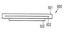
静電チャック600は、図2から分かるように、セラミックスで具備された本体601の内部に、電源が印加される電極602が埋め込まれたものであり、この電極602に高電圧が印加されることにより、本体601の表面に、基板500を付着させるのである。 As can be seen from FIG. 2, the
図1を参照すれば、導入ロボット714は、静電チャック600の上面に基板500を載せ、この状態で静電チャック600は、導入室716に移送され、第1反転ロボット719が、静電チャック600を反転させることによって、蒸着部730では、基板500が下を向くように位置することになる。 Referring to FIG. 1, the
アンローディング部720の構成は、前述のローディング部710の構成と反対に構成される。すなわち、蒸着部730を経た基板500及び静電チャック600を、第2反転室728で第2反転ロボット729が反転させ、搬出室726に移送し、搬出ロボット724が、搬出室726から基板500及び静電チャック600を取り出した後、基板500を静電チャック600から分離し、第2ラック722に積載する。基板500と分離された静電チャック600は、第2循環部620を介して、ローディング部710に回送される。 The configuration of the unloading unit 720 is opposite to the configuration of the
しかし、本発明は、必ずしもこれに限定されるものではなく、基板500が静電チャック600に、最初固定されるときから、静電チャック600の下面に基板500を固定させ、そのまま蒸着部730に移送させることもある。その場合、例えば、第1反転室718及び第1反転ロボット719と、第2反転室728及び第2反転ロボット729は、不要になる。 However, the present invention is not necessarily limited to this, and since the
蒸着部730は、少なくとも1つの蒸着用チャンバを具備する。図1による本発明の一実施形態によれば、前記蒸着部730は、チャンバ731を具備し、このチャンバ731内に、複数の有機層蒸着アセンブリ100,200,300,400が配置される。図1に図示された本発明の一実施形態によれば、前記チャンバ731内に、第1有機層蒸着アセンブリ100、第2有機層蒸着アセンブリ200、第3有機層蒸着アセンブリ300及び第4有機層蒸着アセンブリ400の4個の有機層蒸着アセンブリが設置されているが、その数は、蒸着物質及び蒸着条件によって、可変可能である。前記チャンバ731は、蒸着が進められる間、真空に維持される。 The
一方、図1による本発明の一実施形態によれば、前記基板500が固定された静電チャック600は、第1循環部610によって、少なくとも蒸着部730に、望ましくは、前記ローディング部710、蒸着部730及びアンローディング部720に順次移動され、前記アンローディング部720で、基板500と分離された静電チャック600は、第2循環部620によって、前記ローディング部710に送り戻される。 Meanwhile, according to an exemplary embodiment of the present invention according to FIG. 1, the
前記第1循環部610は、前記蒸着部730を通過するとき、前記チャンバ731を貫通するように具備され、前記第2循環部620は、静電チャックが移送されるように具備される。 The
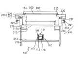
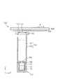
図3は、図1の有機層蒸着装置の第1循環部610及び第1有機層蒸着アセンブリ100を概略的に示す斜視図であり、図4は、図3の側面図(或いはY方向から見た正面図)である。ここで、図3では、説明の便宜のために、チャンバ731が省略された状態で図示されている。さらに、図5は、図3に図示された有機層蒸着装置のチャック移動部材230とガイド部材221とを示す斜視図である。 3 is a perspective view schematically illustrating the
図3ないし図5を参照すれば、本発明の一実施形態に係わる有機層蒸着装置は、第1循環部610と、有機層蒸着アセンブリ100と、を含む。 3 to 5, the organic layer deposition apparatus according to an embodiment of the present invention includes a
詳細には、有機層蒸着アセンブリ100は、蒸着源110、蒸着源ノズル部120及びパターニングスリット・シート150を含む。ここで、蒸着源110は、その内部に蒸着物質115が充填されるルツボ111と、ルツボ111を加熱させ、ルツボ111内部に充填された蒸着物質115を蒸着源ノズル部120側に蒸発させるためのヒータ112と、を含む。一方、蒸着源110の一側には、蒸着源ノズル部120が配置され、蒸着源ノズル部120には、Y軸方向に沿って、複数個の蒸着源ノズル121が形成される。一方、蒸着源110と基板500との間には、パターニングスリット・シート150及びフレーム155がさらに具備され、パターニングスリット・シート150には、X軸方向に沿って、複数個のパターニングスリット151が形成される。本実施形態は、蒸着源110、蒸着源ノズル部120及びパターニングスリット・シート150が、蒸着部730内にそれぞれ別途の部材として形成されもする。これについては、追って詳細に説明する。 In detail, the organic
次に、第1循環部610についてさらに詳細に説明する。第1循環部610は、基板500を固定している静電チャック600を、チャック移動部材230によって移動させる役割を行う。ここで、第1循環部610は、下部プレート213及び上部プレート217を含むフレーム211と、フレーム211の内側に形成されたシート支持台215と、フレーム211上側に形成されたガイド部材221と、前記ガイド部材221の一側に配置された第2磁力発生部240と、ガイド部材221と、チャック移動部材230との間に配置される直線移動(linear motion、LM)ガイド220と、静電チャック600と結合し、前記第2磁力発生部240と対応するように配置される第1磁力発生部231を有するチャック移動部材230と、を含む。静電チャック600とチャック移動部材230は、クランプ250によって、結合または分離が可能である。これについて、さらに詳細に説明すれば、次の通りである。 Next, the
フレーム211は、第1循環部610の基底部をなし、ほぼ中空のボックス状に形成される。ここで、下部プレート213は、前記フレーム211の下部面を形成し、下部プレート213上には、蒸着源110が配置される。一方、上部プレート217は、前記フレーム211の上部面を形成し、蒸着源110で蒸発された蒸着物質115が、パターニングスリット・シート150を通過して基板500に蒸着されるように、上部プレート217には、開口部217aが形成される。このようなフレーム211の各部分は、別途の部材でもって形成されて結合されるか、或いは始めから一体型に形成されてもよい。 The
ここで、図面には、図示されていないが、蒸着源110が配置された下部プレート213は、カセット形式で形成され、フレーム211から外部に引き出されるように形成されもする。従って、蒸着源110の入れ替えが容易になるのである。 Here, although not shown in the drawing, the
一方、シート支持台215は、フレーム211の内側面から突設されもし、パターニングスリット・シート150を支持する役割を行うことができる。また、シート支持台215は、蒸着源ノズル121を介して排出される蒸着物質115が分散されないように、蒸着物質の移動経路をガイドすることもできる。図面には、図示されていないが、シート支持台215の変形例として、ガイド部材221の内側面から突き出し、パターニングスリット・シート150を支持することができる。 On the other hand, the
上部プレート217上に、ガイド部材221が形成される。ガイド部材221は、前記蒸着部730のチャンバ731を貫通するように設置される。ガイド部材221は、一方向(Y軸方向)に沿って長く形成され、一方向(Y軸方向)に沿って対称になるように、一対からなる。ガイド部材221は、チャック移動部材230の移動経路を提供する。 A
ガイド部材221の上部は、ほぼ偏平な平面で形成されてあり、ガイド部材221上部に、チャック移動部材230が配置される。ガイド部材221と、チャック移動部材230との間には、LMガイド220が配置されもする。これについては後述する。 The upper part of the
ガイド部材221の外側面には、第2磁力発生部240が配置され、チャック移動部材230には、第2磁力発生部240に対応するように、第1磁力発生部231が配置される。第1磁力発生部231と、第2磁力発生部240とで形成される磁力によって、チャック移動部材230が、ガイド部材221に沿って移動することになる。 A second magnetic
これについて詳述すれば、第1磁力発生部231は、第2磁力発生部240に対応するように、チャック移動部材230の一面に配置される。第1磁力発生部231は、複数個のマグネット231a,231b,231cが、チャック移動部材230の移動方向(Y軸方向)に沿って一列に配置される。互いに隣接したマグネット231a,231b,231cは、互いに異なる磁性を有するように配列される。すなわち、マグネット231aが、第2磁力発生部240に向けてN極を有するならば、マグネット231aに隣接したマグネット231bは、第2磁力発生部240に向けてS極を有する。また、マグネット231bに隣接したマグネット231cは、第2磁力発生部240に向けてN極を有する。このように、第1磁力発生部231は、N極とS極とが交互に配列された一列のマグネット231a,231b,231c(マグネットレール2311)からなってもよい。 More specifically, the first
マグネット231a,231b,231cは、電磁石、永久磁石または超伝導磁石からなってもよい。 The
第2磁力発生部240は、複数個のマグネットローラ241、シャフト242及びシャフト固定部243を具備することができる。 The second
マグネットローラ241は、螺旋形に捻られた複数個のマグネット241a,241bからなる。マグネット241a,241bは、チャック移動部材230の移動方向(Y軸方向)と同一の方向に捻られる。互いに隣接したマグネット241a,241bは、互いに異なる極性を有する。すなわち、マグネット241aが外側に向かってN極を有するならば、マグネット241aに隣接したマグネット241bは、外側に向かってS極を有する。 The
シャフト242は、複数個のマグネットローラ241を連結する。複数個のマグネットローラ241は、チャック移動部材230の移動方向(Y軸方向)に離隔されて配列され、シャフト242は、チャック移動部材230の移動方向(Y軸方向)に配列された複数個のマグネットローラ241を連結する。シャフト242は、駆動部(図示せず)の駆動力をマグネットローラ241に伝達する。すなわち、シャフト242は、一端で駆動部と連結され、駆動部は、シャフト242を、その長手方向(Y軸方向)を軸として回転させる。シャフト242に連結されたマグネットローラ241は、シャフト242と共に、シャフト242の長手方向を軸として回転することになる。 The
シャフト固定部243は、シャフト242を、ガイド部材221の一側に固定させる。シャフト固定部243は、貫通孔(図示せず)を有し、シャフト242は、前記貫通孔を貫通し、前記貫通孔内で回転自在である。シャフト固定部243は、離隔されたマグネットローラ241間に露出されるシャフト242と結合し、ガイド部材221の外側面に配置されもする。 The
チャック移動部材230と、ガイド部材221との間には、LMガイド220が配置される。LMガイド220は、前記ガイド部材221の一面に配置される1対のガイドレール223と、チャック移動部材230の一面に配置されるガイドブロック225とからなり、ガイドレール223にガイドブロック225が挟まれ、ガイドブロック225が、ガイドレール223に沿って、Y軸方向に往復動することになる。 An
ここで、前記ガイドレール223として、LMレール(linear motion rail)を具備し、前記ガイドブロック225として、LMブロック(linear motion block)を具備し、所定のLMシステム(linear motion system)を構成することができる。LMシステムは、過去の摺動案内システムに比べ、摩擦係数が小さく、位置誤差がほとんど発生せず、位置決定度が非常に高い移送システムであり、本明細書では、このようなLMシステムについては、その詳細な説明を省略する。 Here, the
図5を参照し、ガイド部材221上で移動するチャック移動部材230の動作について説明する。 The operation of the
チャック移動部材230は、第1磁力発生部231と第2磁力発生部240との磁力によって、ガイド部材221に沿って移動する。詳細には、ガイド部材221の外側面に配置された第2磁力発生部240は、複数個のマグネットローラ241と、これらを連結するシャフト242とからなる。シャフト242は、駆動部(図示せず)と連結され、駆動部によって生じた回転力を、マグネットローラ241に伝達し、これによって、マグネットローラ241は、その長手方向(Y軸方向)を軸として回転することになる。マグネットローラ241は、前述のように、マグネット241a,241bが互いに捻れて螺旋形をなす。マグネットローラ241の回転によって、マグネット241a,241bによって生じる磁場は、螺旋形の方向に沿って移動する。移動する磁場によって、マグネット231a,231b,231cが配置されたチャック移動部材230は、ガイド部材221に沿って移動する。 The
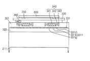
図6は、本発明の他の実施形態に係わる有機層蒸着装置の第1循環部610’及び有機層蒸着アセンブリ100を示す斜視図であり、図7は、図6に図示された有機層蒸着装置の第1循環部610’及び有機層蒸着アセンブリ100をY軸方向から見た正面図であり、図8は、図6に図示された有機層蒸着装置の第1循環部610’及び有機層蒸着アセンブリ100を示す側面図(X軸方向から見た)である。図9は、図6に図示された有機層蒸着装置のチャック移動部材330とガイド部材321とを示す斜視図である。 FIG. 6 is a perspective view illustrating a
図6ないし図8を参照すれば、本発明の他の実施形態による有機層蒸着装置は、第1循環部610’と、有機層蒸着アセンブリ100とを含む。 Referring to FIGS. 6 to 8, the organic layer deposition apparatus according to another embodiment of the present invention includes a
図6に図示された有機層蒸着アセンブリ100は、図3に図示された有機層蒸着アセンブリ100のように、蒸着源110、蒸着源ノズル部120及びパターニングスリット・シート150を含む。これらに係わる説明はすでに行ったので、以下では省略する。 The organic
第1循環部610’は、基板500を固定している静電チャック600を、チャック移動部材330によって移動させる役割を行う。ここで、第1循環部610’は、下部プレート213及び上部プレート217を含むフレーム211と、フレーム211の内側に形成されたシート支持台215と、フレーム211の上側に形成されたガイド部材321及びガイド補助部材322と、前記ガイド補助部材322の一側に配置された第2磁力発生部331と、ガイド部材321とチャック移動部材330との間に配置されるLMガイド220と、静電チャック600と結合し、前記第2磁力発生部331と対応するように配置される第1磁力発生部340を有するチャック移動部材330と、を含む。これについて、さらに詳細に説明すれば、次の通りである。 The
上部プレート217上に、ガイド部材321が形成され、ガイド部材321の外側面には、ガイド補助部材322が形成される。ガイド部材321及びガイド補助部材322は、前記蒸着部730のチャンバ731を貫通するように設置される。ガイド部材321及びガイド補助部材322は、一方向(Y軸方向)に沿って長く形成され、一方向(Y軸方向)に対称になるように、一対からなる。ガイド部材321は、チャック移動部材330の移動経路を提供する。ガイド補助部材322上には、第2磁力発生部331が配置される。 A
ガイド部材321の上部は、ほぼ偏平な平面で形成されており、ガイド部材321の上部に、チャック移動部材330が配置される。ガイド部材321と、チャック移動部材330との間には、LMガイド220が配置される。これについては後述する。 The upper part of the
ガイド部材321の外側面には、ガイド補助部材322が配置される。ガイド部材321と、ガイド補助部材322は、別途に形成されてもよいし、または一体に形成されてもよい。ガイド補助部材322の一面には、第1磁力発生部340に対応するように、第2磁力発生部331が配置され、チャック移動部材330には、第2磁力発生部331に対応するように、第1磁力発生部340が配置される。第1磁力発生部340と、第2磁力発生部331とで形成される磁力によって、チャック移動部材330が、ガイド部材321に沿って移動することになる。 A guide
これについて詳述すれば、第2磁力発生部331は、第1磁力発生部340に対応するように、ガイド補助部材322の一面に配置される。第2磁力発生部331は、複数個のマグネット331a,331b,331cが、チャック移動部材330の移動方向(Y軸方向)に沿って一列に配置される。互いに隣接したマグネット331a,331b,331cは、互いに異なる極性を有するように配列される。すなわち、マグネット331aが、第1磁力発生部340に向けてN極を有するならば、マグネット331aに隣接したマグネット331bは、第1磁力発生部340に向けてS極を有する。また、マグネット331bに隣接したマグネット331cは、第1磁力発生部340に向けてN極を有する。このように、第2磁力発生部331は、N極とS極とが交互に配列された一列のマグネット331a,331b,331c(マグネットレール3311)からなってもよい。 More specifically, the second
マグネット331a,331b,331cは、電磁石、永久磁石または超伝導磁石からなってもよい。 The
第1磁力発生部340は、複数個のマグネットローラ341、シャフト342及びシャフト固定部343を具備することができる。 The first
マグネットローラ341は、螺旋形に捻られた複数個のマグネット341a,341b(図9)からなる。マグネット341a,341bは、チャック移動部材330の移動方向(Y軸方向)と同一の方向に捻られる。互いに隣接したマグネット341a,341bは、互いに異なる極性を有する。すなわち、マグネット341aが外側に向かってN極を有するならば、マグネット341aに隣接したマグネット341bは、外側に向かってS極を有する。 The
シャフト342は、複数個のマグネットローラ341を連結する。複数個のマグネット341は、チャック移動部材330の移動方向(Y軸方向)に離隔されて配列され、シャフト342は、チャック移動部材330の移動方向(Y軸方向)に配列された複数個のマグネット341を連結する。シャフト342は、駆動部360の駆動力をマグネットローラ341に伝達する。すなわち、シャフト342は、一端で駆動部360と連結され、駆動部360は、シャフト342をその長手方向(Y軸方向)を軸として回転させる。シャフト342に連結されたマグネットローラ341は、シャフト342と共に、シャフト342の長手方向を軸として回転することになる。 The
シャフト固定部343は、シャフト342を、ガイド補助部材322の一側に固定させる。シャフト固定部343は、貫通孔(図示せず)を有し、シャフト342は、前記貫通孔を貫通し、前記貫通孔内で回転自在である。シャフト固定部343は、離隔されたマグネットローラ341間に露出されるシャフト342と結合し、ガイド補助部材322の外側面に配置されもする。 The
チャック移動部材330と、ガイド部材321との間には、LMガイド220が配置されもする。LMガイド220は、前記ガイド部材321の一面に配置される1対のガイドレール223と、チャック移動部材330の一面に配置されるガイドブロック225とからなり、ガイドレール223にガイドブロック225が挟まれ、ガイドブロック225がガイドレール223に沿って往復動することになる。ここで、前記ガイドレール223として、LMレールを具備し、前記ガイドブロック225として、LMブロックを具備し、所定のLMシステムを構成することができる。LMシステムは、過去の摺動案内システムに比べ、摩擦係数が小さく、位置誤差がほとんど発生せず、位置決定度が非常に高い移送システムであり、本明細書では、このようなLMシステムについては、その詳細な説明を省略する。 An
図9を参照し、ガイド部材321上で移動するチャック移動部材330の動作について説明する。 The operation of the
チャック移動部材330は、第1磁力発生部340と、第2磁力発生部331との磁力によって、ガイド部材321に沿って移動する。詳細には、チャック移動部材330の一面に配置された第1磁力発生部340は、複数個のマグネットローラ341と、これらを連結するシャフト342と、回転力を発生させる駆動部360とからなる。シャフト342は、駆動部360と連結され、駆動部360によって生じた回転力を、マグネットローラ341に伝達し、これによって、マグネットローラ341は、その長手方向(Y軸方向)を軸として回転することになる。マグネットローラ341は、前述のように、マグネット341a,341bが互いに捻れて螺旋形をなす。マグネットローラ341の回転によって、マグネット341a,341bによって生じる磁場は、ガイド補助部材322の一面に配置される第2磁力発生部331のマグネットレール3311のマグネット331a,331b,331cによる磁場に対して、第1磁力発生部340自身が配置されたチャック移動部材330をガイド部材321に沿って移動する推進力を発生することになる。 The
図6ないし図9に図示された有機層蒸着装置は、駆動部360をチャック移動部材330に付着させるために、チャック移動部材330が独立して制御される。また、ガイド補助部材322に沿って、マグネットレール3311が一列に配列されるので、チャック移動部材330は、さらに安定してガイド部材321に沿って移動することになる。 In the organic layer deposition apparatus shown in FIGS. 6 to 9, the
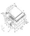
図10ないし図12を参照すれば、本発明の一実施形態に係わる有機層蒸着アセンブリ700は、蒸着源110、蒸着源ノズル部702、遮断板アセンブリ130及びパターニングスリット・シート150を含む。 10 to 12, an organic
ここで、図10ないし図12には、説明の便宜のために、チャンバを図示していないが、図10ないし図12のあらゆる構成は、適切な真空度が維持されるチャンバ内に配置されることが望ましい。それは、蒸着物質の直進性を確保するためである。 Here, for convenience of explanation, the chamber is not shown in FIGS. 10 to 12, but all the configurations of FIGS. 10 to 12 are disposed in a chamber in which an appropriate degree of vacuum is maintained. It is desirable. This is to ensure straightness of the vapor deposition material.
このようなチャンバ内には、被蒸着体である基板500が、静電チャック600によって移送される。前記基板500は、平板表示装置用基板にもなるが、多数の平板表示装置を形成することができるマザーガラス(mother glass)のような大面積基板が適用されもする。 In such a chamber, a
ここで、本発明の一実施形態では、基板500が有機層蒸着アセンブリ700に対して、相対的に移動するが、望ましくは、有機層蒸着アセンブリ700に対して、基板500を矢印A方向に移動させることができる。 Here, in one embodiment of the present invention, the
詳細には、既存のファインメタルマスク(fine metal mask、FMM)蒸着方法では、マスクの大きさが、基板サイズと同一であるか、あるいはそれよりも大きくなければならない。従って、基板サイズが増大するほど、マスクも大型化してしまった。このような大型のマスクの製作は、容易ではなく、さらにマスクを引っ張って精緻なパターンにアライン(align)するのも、容易ではないという問題点が従来、存在した。 In detail, in the existing fine metal mask (FMM) deposition method, the size of the mask must be the same as or larger than the substrate size. Therefore, the larger the substrate size, the larger the mask. Conventionally, it is not easy to manufacture such a large mask, and it is not easy to pull the mask and align it into a fine pattern.
このような問題点を解決するために、本発明の一実施形態に係わる有機層蒸着アセンブリ700は、有機層蒸着アセンブリ700と基板500とが互いに相対的に移動しつつ、蒸着がなされることを一つの特徴とする。言い換えれば、有機層蒸着アセンブリ700と対面するように配置された基板500が、Y軸方向に沿って移動しつつ、連続的に蒸着を行う。すなわち、基板500が、図10の矢印A方向に移動しつつ、スキャニング(scanning)方式で蒸着が行われるのである。ここで図面には、基板500が、チャンバ731(図1)内で、Y軸方向に移動しつつ、蒸着がなされると図示されているが、本発明の思想は、これに制限されるものではなく、基板500は、固定されてあり、有機層蒸着アセンブリ700自体が、Y軸方向に移動しつつ蒸着を行うことも可能である。 In order to solve such problems, the organic
従って、本発明の有機層蒸着アセンブリ700では、従来のFMMに比べて、はるかに小さくパターニングスリット・シート150を設けることが可能である。すなわち、本発明の有機層蒸着アセンブリ700の場合、基板500がY軸方向に沿って移動しつつ、連続して、すなわち、スキャニング方式で蒸着を行うので、パターニングスリット・シート150のX軸方向への幅を、基板500のX軸方向への幅とのみ実質的に等しく形成すればよく、パターニングスリット・シート150のY軸方向の長さは、基板500の長さより、はるかに小さく形成しても差し支えない。もちろん、パターニングスリット・シート150のX軸方向への幅が、基板500のX軸方向への幅より小さく形成されても、基板500と有機層蒸着アセンブリ700とのX軸方向への相対的移動によるスキャニング方式によって、十分に基板500全体に対して蒸着を行うことができる。 Accordingly, the organic
このように、従来のFMMに比べて、はるかに小さくパターニングスリット・シート150を設けることが可能であるので、本発明のパターニングスリット・シート150は、その製造が容易である。すなわち、パターニングスリット・シート150のエッチング作業や、その後の精密引っ張り及び溶接の作業、移動及び洗浄の作業などのあらゆる工程で、小サイズのパターニングスリット・シート150が、FMM蒸着方法に比べて有利である。また、それは、ディスプレイ装置が大型化されるほど、さらに有利になる。 Thus, since the
このように、有機層蒸着アセンブリ700と基板500とが、互いに相対的に移動しつつ蒸着がなされるためには、有機層蒸着アセンブリ700と基板500とが、一定程度離隔されることが望ましい。これについては、追って詳細に記述する。 As described above, in order to perform the deposition while the organic
一方、チャンバ内で前記基板500と対向する側には、蒸着物質115が収納及び加熱される蒸着源110が配置される。 Meanwhile, a
前記蒸着源110は、その内部に、蒸着物質115が充填されるルツボ111と、該ルツボ111を加熱させるヒータ112とが具備される。 The
蒸着源110の一側、詳細には、蒸着源110から基板500に向かう側には、蒸着源ノズル部702が配置される。そして、蒸着源ノズル部702には、X軸方向に沿って、複数個の蒸着源ノズル703が形成される。ここで、前記複数個の蒸着源ノズル703は、等間隔で形成されもする。蒸着源110内で気化された蒸着物質115は、このような蒸着源ノズル部702の蒸着源ノズル703を通過し、被蒸着体である基板500側に向かうことになる。 On one side of the
蒸着源ノズル部702の一側には、遮断板アセンブリ130が具備される。前記遮断板アセンブリ130は、複数枚の遮断板131と、遮断板131の外側に具備される遮断板フレーム132とを含む。前記複数枚の遮断板131は、X軸方向に沿って、互いに平行に配置されもする。ここで、前記複数枚の遮断板131は、等間隔で形成されもする。また、それぞれの遮断板131は、図面で見るとき、YZ平面に沿って延長されており、望ましくは、長方形に具備される。このように配置された複数枚の遮断板131は、蒸着源ノズル部702と、パターニングスリット・シート150との間の空間を、複数個の蒸着空間S(図12)で仕切る。すなわち、本発明の一実施形態に係わる有機層蒸着アセンブリ700では、前記遮断板131によって、図12から分かるように、蒸着物質が噴射されるそれぞれの蒸着源ノズル703別に蒸着空間Sが分離される。 A
ここで、それぞれの遮断板131は、互いに隣接している蒸着源ノズル703間に配置されもする。それは言い換えれば、互いに隣接している遮断板131間に、1つの蒸着源ノズル703が配置されるのである。望ましくは、蒸着源ノズル703は、互いに隣接している遮断板131間の真ん中に位置することができる。しかし、本発明は、必ずしもそれに限定されるものではなく、互いに隣接している遮断板131間に、複数の蒸着源ノズル703が配置されても差し支えない。ただし、その場合にも、複数の蒸着源ノズル703を、互いに隣接している遮断板131間の真ん中付近にそれぞれ位置させることが望ましい。 Here, the
このように、遮断板131が、蒸着源ノズル部702と、パターニングスリット・シート150との間の空間を複数個の蒸着空間Sに仕切ることにより、1つの蒸着源ノズル703から排出される蒸着物質は、異なる蒸着源ノズル703から排出された蒸着物質と混合せず、パターニングスリット151を通過して、基板500に蒸着されるのである。すなわち、前記遮断板131は、各蒸着源ノズル703を介して排出される蒸着物質が分散せずに、Z軸方向に直進するように、蒸着物質の移動経路をガイドする役割を果たす。 As described above, the shielding
このように遮断板131を具備し、蒸着物質の直進性を確保することにより、基板に形成される陰影(shadow)の大きさを大幅に縮めることができ、従って、有機層蒸着アセンブリ700と基板500とを一定程度離隔させることが可能になる。これについては後述する。 Thus, by providing the
一方、蒸着源110と基板500との間には、パターニングスリット・シート150及びフレーム155がさらに具備される。前記フレーム155は、ほぼ略窓フレームのような形態で形成され、その内側に、パターニングスリット・シート150が結合される。そして、パターニングスリット・シート150には、X軸方向に沿って、複数個のパターニングスリット151が形成される。各パターニングスリット151は、Y軸方向に沿って延びている。蒸着源110内で気化され、蒸着源ノズル703を通過した蒸着物質115は、パターニングスリット151を通過し、被蒸着体である基板500側に向かうことになる。 Meanwhile, a
前記パターニングスリット・シート150は、金属薄板で形成され、引っ張られた状態で、フレーム155に固定される。前記パターニングスリット151は、ストライプタイプ(stripe type)に、パターニングスリット・シート150に、エッチングを介して形成される。ここで、前記パターニングスリット151の個数は、基板500に形成される蒸着パターンの個数に対応させることが望ましい。 The
一方、前述の遮断板アセンブリ130と、パターニングスリット・シート150は、互いに一定程度離隔されるように形成され、遮断板アセンブリ130と、パターニングスリット・シート150は、別途の連結部材135によって互いに連結される。 Meanwhile, the blocking
前述のように、本発明の一実施形態に係わる有機層蒸着アセンブリ700は、基板500に対して、相対的に移動しつつ蒸着を行い、このように、有機層蒸着アセンブリ700が基板500に対して、相対的に移動するためパターニングスリット・シート150は、基板500から、一定程度離隔されるように形成される。そして、パターニングスリット・シート150と基板500とを離隔させる場合に発生する陰影問題を解決するために、蒸着源ノズル部702と、パターニングスリット・シート150との間に、遮断板131を具備し、蒸着物質の直進性を確保することにより、基板に形成される陰影の大きさを大幅に縮めたのである。 As described above, the organic
従来のFMM蒸着方法では、基板に陰影を生じさせないように、基板にマスクを密着させて蒸着工程を進めた。しかし、このように、基板にマスクを密着させる場合、基板とマスクとの接触によって、基板にすでに形成されていたパターンが引っ掻かれるような不良問題が発生するという問題点が存在した。また、マスクを基板に対して移動させることができないため、マスクが基板と同一の大きさに形成されなければならなかった。従って、ディスプレイ装置が大型化されることによって、マスクサイズも大きくならなければならず、このような大型マスクを形成することが容易ではないという問題点が存在した。 In the conventional FMM vapor deposition method, the vapor deposition process was performed with a mask in close contact with the substrate so as not to cause a shadow on the substrate. However, when the mask is brought into close contact with the substrate as described above, there has been a problem that a defect problem occurs in which the pattern already formed on the substrate is scratched by the contact between the substrate and the mask. Further, since the mask cannot be moved with respect to the substrate, the mask has to be formed in the same size as the substrate. Therefore, as the display device is increased in size, the mask size must be increased, and there is a problem that it is not easy to form such a large mask.
このような問題点を解決するために、本発明の一実施形態に係わる有機層蒸着アセンブリ700では、パターニングスリット・シート150が、被蒸着体である基板500と所定間隔を置いて離隔されるように配置される。それは、遮断板131を具備し、基板500に生成される陰影が小くなることによって実現可能になる。 In order to solve such a problem, in the organic
また、本発明によって、マスクを基板より小さく形成した後、マスクを基板に対して移動させつつ蒸着を行うことができることにより、マスク製作が容易になるという効果を得ることができる。また、基板とマスクとの接触による不良を防止する効果を得ることができる。また、製造工程にあって、基板とマスクとを密着させる時間が不要になるので、製造速度が向上するという効果を得ることができる。 In addition, according to the present invention, after the mask is formed to be smaller than the substrate, it is possible to perform deposition while moving the mask with respect to the substrate, so that an effect of facilitating mask manufacture can be obtained. In addition, it is possible to obtain an effect of preventing defects due to contact between the substrate and the mask. In addition, in the manufacturing process, since the time for bringing the substrate and the mask into close contact with each other is not necessary, an effect of improving the manufacturing speed can be obtained.
また、有機層蒸着アセンブリ700を構成する蒸着源110、蒸着源ノズル部702及びパターニングスリット・シート150が一体に形成されるのではなく、蒸着部730内に、それぞれ別途の部材として形成される。このような構成によって、蒸着物質115充填のための蒸着源110の引き入れ及び引き出し、洗浄または入れ替えのためのパターニングスリット・シート150の引き入れ及び引き出しなどが容易に行われるという効果を得ることができる。 Further, the
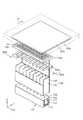
図13は、本発明の他の一実施形態に係わる有機層蒸着アセンブリ800を概略的に図示した斜視図である。 FIG. 13 is a perspective view schematically illustrating an organic
図13に図示された実施形態に係わる有機層蒸着アセンブリ800は、蒸着源110、蒸着源ノズル部702、第1遮断板アセンブリ130、第2遮断板アセンブリ840、パターニングスリット・シート150を含む。ここで、蒸着源110、第1遮断板アセンブリ130及びパターニングスリット・シート150の詳細な構成は、前述の図3による実施形態と同一であるので、詳細な説明を省略する。本実施形態では、第1遮断板アセンブリ130の一側に、第2遮断板アセンブリ840が具備されるという点で、前述の実施形態と区別される。 The organic
詳細には、前記第2遮断板アセンブリ840は、複数枚の第2遮断板841と、第2遮断板841の外側に具備される第2遮断板フレーム842と、を含む。前記複数枚の第2遮断板841は、X軸方向に沿って互いに平行に具備される。そして、前記複数枚の第2遮断板841は、等間隔で形成される。また、それぞれの第2遮断板841は、図面で見るとき、YZ平面と平行になるように、言い換えれば、X軸方向に垂直になるように形成される。 In detail, the second shield plate assembly 840 includes a plurality of second shield plates 841 and a second
このように配置された複数枚の第1遮断板131及び第2遮断板841は、蒸着源ノズル部702と、パターニングスリット・シート150との間の空間を仕切る役割を行う。すなわち、前記第1遮断板131及び第2遮断板841によって、蒸着物質が噴射されるそれぞれの蒸着源ノズル703別に、蒸着空間が分離することを一つの特徴とする。 The plurality of
ここで、それぞれの第2遮断板841は、それぞれの第1遮断板131と一対一に対応するように配置されもする。言い換えれば、それぞれの第2遮断板841は、それぞれの第1遮断板131とアラインされて互いに平行に配置されもする。すなわち、互いに対応する第1遮断板131と第2遮断板841は、互いに同一の平面上に位置することになるのである。図面には、第1遮断板131の幅と、第2遮断板841のX軸方向の幅とが同一であるように図示されているが、本発明の思想は、これに制限されるものではない。すなわち、パターニングスリット151との精緻なアラインが要求される第2遮断板841は、相対的に薄く形成される一方、精緻なアラインが要求されない第1遮断板131は、相対的に厚く形成され、その製造を容易にすることも可能なのである。 Here, each of the second blocking plates 841 may be disposed to correspond to each of the
図14は、本発明のさらに他の一実施形態による有機層蒸着アセンブリ900を概略的に図示した斜視図である。 FIG. 14 is a perspective view schematically illustrating an organic
図14を参照すれば、本発明のさらに他の一実施形態による有機層蒸着アセンブリ900は、蒸着源910、蒸着源ノズル部920及びパターニングスリット・シート950を含む。 Referring to FIG. 14, an organic
ここで、蒸着源910は、その内部に蒸着物質915が充填されるルツボ911と、ルツボ911を加熱させ、ルツボ911内部に充填された蒸着物質915を、蒸着源ノズル部920側に蒸発させるためのヒータ912と、を含む。一方、蒸着源910の一側には、蒸着源ノズル部920が配置され、蒸着源ノズル部920には、Y軸方向に沿って、複数個の蒸着源ノズル921が形成される。一方、蒸着源910と基板500との間には、パターニングスリット・シート950及びフレーム955がさらに具備され、パターニングスリット・シート950には、X軸方向に沿って、複数個のパターニングスリット951及びスペーサ(図示せず)が形成される。そして、蒸着源910、蒸着源ノズル部920及びパターニングスリット・シート950は、連結部材935によって結合される。 Here, the
本実施形態は、前述の実施形態に比べ、蒸着源ノズル部920に具備された複数個の蒸着源ノズル921の配置が異なっているが、これについて詳細に説明する。 This embodiment is different from the above-described embodiment in the arrangement of the plurality of vapor
蒸着源910の一側、詳細には、蒸着源910から基板500に向かう側には、蒸着源ノズル部920が配置される。そして、蒸着源ノズル部920には、Y軸方向、すなわち基板500のスキャン方向に沿って、複数個の蒸着源ノズル921が形成される。ここで、前記複数個の蒸着源ノズル921は、等間隔で形成されもする。蒸着源910内で気化された蒸着物質915は、このような蒸着源ノズル部920を通過し、被蒸着体である基板500側に向かうことになる。このように、蒸着源ノズル部920上に、Y軸方向、すなわち、基板500のスキャン方向に沿って、複数個の蒸着源ノズル921が形成される場合、パターニングスリット・シート950のそれぞれのパターニングスリット951を通過する蒸着物質によって形成されるパターンの大きさは、蒸着源ノズル921の大きさ一つによってのみ影響を受けるので(すなわち、X軸方向には、蒸着源ノズル921が一つだけ存在する)、陰影が発生しない。また、多数個の蒸着源ノズル921が、スキャン方向に存在するので、個別蒸着源ノズル間のフラックス(flux)差が生じても、その差が相殺され、蒸着均一度が一定に維持されるという効果を得ることができる。併せて、図10などに図示された実施形態に具備された遮断板アセンブリが具備されないから、遮断板アセンブリに蒸着物質が蒸着されず、蒸着物質の利用効率が向上するという効果を得ることができる。 On one side of the
図15は、本発明の有機層蒸着装置を利用して製造されたアクティブマトリックス型有機発光ディスプレイ装置の断面を図示したものである。 FIG. 15 illustrates a cross section of an active matrix organic light emitting display device manufactured using the organic layer deposition apparatus of the present invention.
図15を参照すれば、前記アクティブマトリックス型の有機発光ディスプレイ装置10は、図1乃至図14で示した基板500上に形成される。なお、図15では、基板30として示す。基板30(500)は、透明な素材、例えば、ガラス材、プラスチック材、または金属材で形成される。前記基板30上には、全体的にバッファ層のような絶縁膜31が形成されている。 Referring to FIG. 15, the active matrix organic light emitting
前記絶縁膜31上には、薄膜トランジスタ(TFT)40と、キャパシタ50と、有機発光素子60とが形成される。 A thin film transistor (TFT) 40, a
前記絶縁膜31の上面には、所定パターンに配列された半導体活性層41が形成されている。前記半導体活性層41は、ゲート絶縁膜32によって埋め込まれている。前記活性層41は、p型またはn型の半導体でなる。 A semiconductor
前記ゲート絶縁膜32の上面には、前記活性層41と対応するところに、TFT40のゲート電極42が形成される。そして、前記ゲート電極42を覆うように、層間絶縁膜33が形成される。前記層間絶縁膜33が形成された後には、ドライエッチングなどのエッチング工程によって、前記ゲート絶縁膜32と層間絶縁膜33とをエッチングしてコンタクトホールを形成させ、前記活性層41の一部を露出させる。 A
その後、前記層間絶縁膜33上に、ソース/ドレイン電極43が形成される。詳細には、コンタクトホールを介して露出された活性層41に接触されるようにソース/ドレイン電極43が形成される。前記ソース/ドレイン電極43を覆うように、保護膜34が形成され、エッチング工程を介して、前記ドレイン電極43の一部を露出させる。前記保護膜34上には、保護膜34の平坦化のために、別途の絶縁膜をさらに形成しもする。 Thereafter, source /
一方、前記有機発光素子60は、電流の流れによって、赤色、緑色、青色の光を発光し、所定の画像情報を表示するためのものとして、前記保護膜34上に、第1電極61を形成する。前記第1電極61は、TFT40のドレイン電極43と電気的に連結される。 On the other hand, the organic light emitting element 60 emits red, green, and blue light according to the flow of current, and forms a first electrode 61 on the protective film 34 for displaying predetermined image information. To do. The first electrode 61 is electrically connected to the
そして、前記第1電極61を覆うように、画素定義膜35が形成される。この画素定義膜35に、所定の開口を形成した後、この開口で限定された領域内に、発光層を含む有機層63を形成する。そして、有機層63上には、第2電極62を形成する。 A
前記画素定義膜35は、各画素を区画することにより、有機物で形成され、第1電極61が形成されている基板の表面、特に、保護層34の表面を平坦化する。 The
前記第1電極61と第2電極62は、互いに絶縁されており、発光層を含む有機層63に、互いに異なる極性の電圧を加えて発光を行わせる。 The first electrode 61 and the second electrode 62 are insulated from each other, and emit light by applying voltages of different polarities to the organic layer 63 including the light emitting layer.
前記発光層を含む有機層63は、低分子または高分子の有機物が使われるが、低分子有機物を使う場合、正孔注入層(HIL:hole injection layer)、正孔輸送層(HTL:hole transport layer)、発光層(EML:emission layer)、電子輸送層(ETL:electron transport layer)、電子注入層(EIL:electron injection layer)などが、単一あるいは複合の構造で積層されて形成され、使用可能な有機材料も、銅フタロシアニン(CuPc)、N,N−ジ(ナフタレン−1−イル)−N,N’−ジフェニル−ベンジジン(NPB)、トリス−8−ヒドロキシキノリンアルミニウム(Alq3)などを含んで多様に適用可能である。 For the organic layer 63 including the light emitting layer, a low molecular or high molecular organic substance is used. When a low molecular organic substance is used, a hole injection layer (HIL) or a hole transport layer (HTL) is used. layer, light-emitting layer (EML), electron transport layer (ETL), electron injection layer (EIL), etc. are formed by laminating and using a single or composite structure Possible organic materials also include copper phthalocyanine (CuPc), N, N-di (naphthalen-1-yl) -N, N′-diphenyl-benzidine (NPB), tris-8-hydroxyquinoline aluminum (Alq3), etc. It can be applied in various ways.
このような有機発光膜を形成した後には、第2電極62も、同一の蒸着工程で形成することができる。 After such an organic light emitting film is formed, the second electrode 62 can also be formed by the same vapor deposition process.
一方、前記第1電極61は、アノード電極の機能を担い、前記第2電極62は、カソード電極の機能を担うが、もちろん、これら第1電極61と第2電極62との極性は、反対になっても差し支えない。そして、第1電極61は、各画素の領域に対応するようにパターニングされ、第2電極62は、あらゆる画素を覆うように形成されもする。 On the other hand, the first electrode 61 functions as an anode electrode, and the second electrode 62 functions as a cathode electrode. Of course, the polarities of the first electrode 61 and the second electrode 62 are opposite to each other. It doesn't matter if it becomes. The first electrode 61 is patterned so as to correspond to the area of each pixel, and the second electrode 62 may be formed so as to cover all the pixels.
前記第1電極61は、透明電極または反射型電極で具備されもするが、透明電極として使われるときには、酸化インジウムスズ(ITO)、酸化インジウム亜鉛(IZO)、ZnOまたはIn2O3で具備され、反射型電極で使われるときには、Ag、Mg、Al、Pt、Pd、Au、Ni、Nd、Ir、Cr、及びそれらの化合物などで反射層を形成した後、その上にITO、IZO、ZnOまたはIn2O3で透明電極層を形成することができる。このような第1電極61は、スパッタリング法などによって成膜された後、フォトリソグラフィ法などによってパターニングされる。The first electrode 61 may be a transparent electrode or a reflective electrode, but when used as a transparent electrode, the first electrode 61 is made of indium tin oxide (ITO), indium zinc oxide (IZO), ZnO, or In2 O3. When a reflective electrode is used, a reflective layer is formed of Ag, Mg, Al, Pt, Pd, Au, Ni, Nd, Ir, Cr, and their compounds, and then ITO, IZO, ZnO is formed thereon. Alternatively, the transparent electrode layer can be formed of In2 O3 . Such a first electrode 61 is formed by sputtering or the like and then patterned by photolithography or the like.
一方、前記第2電極62も、透明電極または反射型電極として具備されもするが、透明電極として使われるときには、この第2電極62が、カソード電極として使われるので、仕事関数の小さい金属、すなわち、Li、Ca、LiF/Ca、LiF/Al、Al、Ag、Mg、及びそれらの化合物が、発光層を含む有機層63の方向に向かうように蒸着された後、その上にITO、IZO、ZnOまたはIn2O3などで補助電極層やバス電極ラインを形成することができる。そして、反射型電極として使われるときには、前記のLi、Ca、LiF/Ca、LiF/Al、Al、Ag、Mg、及びそれらの化合物を全面蒸着して形成する。このとき、蒸着は、前述の発光層を含む有機層63の場合と同様の方法で行うことができる。On the other hand, the second electrode 62 may also be provided as a transparent electrode or a reflective electrode. However, when the second electrode 62 is used as a transparent electrode, the second electrode 62 is used as a cathode electrode. , Li, Ca, LiF / Ca, LiF / Al, Al, Ag, Mg, and their compounds are vapor-deposited in the direction of the organic layer 63 including the light-emitting layer, and then ITO, IZO, An auxiliary electrode layer and a bus electrode line can be formed of ZnO or In2 O3 . When used as a reflective electrode, it is formed by vapor-depositing the entire surface of Li, Ca, LiF / Ca, LiF / Al, Al, Ag, Mg, and their compounds. At this time, the vapor deposition can be performed in the same manner as in the case of the organic layer 63 including the light emitting layer.
本発明は、これらの他にも、有機TFTの有機層または無機膜などの蒸着にも使うことができ、その他、多様な素材の成膜工程に適用可能である。 In addition to these, the present invention can be used for vapor deposition of an organic layer or an inorganic film of an organic TFT, and can be applied to a film forming process of various other materials.
図16は、有機層蒸着装置で、パターニングスリット・シートにパターニングスリットが等間隔で形成されている様子を示す図であり、図17は、図16のパターニングスリット・シートを利用して基板上に形成された有機層を示す図である。 FIG. 16 is a diagram illustrating a state in which patterning slits are formed at equal intervals on the patterning slit sheet in the organic layer deposition apparatus, and FIG. 17 is a diagram illustrating the patterning slit sheet on FIG. It is a figure which shows the formed organic layer.
図16及び図17には、パターニングスリット151が等間隔で配置されたパターニングスリット・シート150が図示されている。すなわち、図16で、l1=l2=l3=l4の関係が成立する。 16 and 17 illustrate a
その場合、中心線Cを通過する蒸着物質の入射角度は、基板500にほぼ垂直になる。従って、パターニングスリット151aを通過した蒸着物質によって形成される有機層P1は、その陰影の大きさは最小になり、右側の陰影SR1と左側の陰影SL1とが対称をなすように形成される。In that case, the incident angle of the vapor deposition material passing through the center line C is substantially perpendicular to the
しかし、中心線Cから遠く配置されたパターニングスリットを通過する蒸着物質の臨界入射角度θは、だんだんと大きくなり、最も終端部のパターニングスリット151eを通過する蒸着物質の臨界入射角度θは、およそ55°になる。従って、蒸着物質がパターニングスリット151eに対して傾いて入射し、パターニングスリット151eを通過した蒸着物質によって形成された有機層P5は、その陰影の大きさが最大になり、特に、左側の陰影SL5が、右側の陰影SR5よりさらに長く形成される。However, the critical incident angle θ of the vapor deposition material passing through the patterning slit disposed far from the center line C gradually increases, and the critical incident angle θ of the vapor deposition material passing through the
すなわち、蒸着物質の臨界入射角度θが大きくなることにより、陰影の大きさも大きくなり、特に、中心線Cから遠い方の陰影の大きさが大きくなる。そして、蒸着物質の臨界入射角度θは、中心部からパターニングスリットまでの距離が遠いほど大きくなることになる。従って、中心線Cからパターニングスリットまでの距離が遠い有機層であればあるほど、陰影の大きさが大きくなり、特に、有機層の両端部の陰影のうち、蒸着空間Sの中心線Cから遠い方の陰影の大きさがさらに大きくなる。 That is, as the critical incident angle θ of the vapor deposition material increases, the size of the shadow also increases, and in particular, the size of the shadow farther from the center line C increases. The critical incident angle θ of the vapor deposition material increases as the distance from the central portion to the patterning slit increases. Accordingly, the farther the organic layer is from the center line C to the patterning slit, the larger the shadow becomes. In particular, among the shadows at both ends of the organic layer, the farther from the center line C of the deposition space S. The size of the shadow on the side becomes even larger.
すなわち、図17で見るとき、中心線Cを基準に、左側に形成された有機層は、左側斜辺が右側斜辺よりさらに長く形成され、中心線Cを基準に、右側に形成された有機層は、右側斜辺が左側斜辺よりさらに長く形成される。 That is, when viewed in FIG. 17, the organic layer formed on the left side with respect to the center line C has a left oblique side longer than the right oblique side, and the organic layer formed on the right side with respect to the center line C is The right hypotenuse is formed longer than the left hypotenuse.
また、中心線Cを基準に、左側に形成された有機層は、左側に形成された有機層であればあるほど、左側斜辺の長さがさらに長く形成され、中心線Cを基準に、右側に形成された有機層は、右側に形成された有機層であればあるほど、右側斜辺の長さがさらに長く形成される。そして、結果として、蒸着空間S内に形成された有機層は、中心線を基準に対称をなすように形成されもする。 In addition, the organic layer formed on the left side with respect to the center line C has a longer left oblique side as the organic layer is formed on the left side, and the right side with respect to the center line C. As the organic layer formed on the right side is the organic layer formed on the right side, the length of the right oblique side is further increased. As a result, the organic layer formed in the vapor deposition space S may be formed to be symmetric with respect to the center line.
これについてさらに詳細に説明すれば、次の通りである。パターニングスリット151bを通過する蒸着物質は、θbの臨界入射角でパターニングスリット151bを通過し、その場合、パターニングスリット151bを通過した蒸着物質によって形成された有機層P2の左側陰影は、SL2の大きさに形成される。同様に、パターニングスリット151cを通過する蒸着物質は、θcの臨界入射角でパターニングスリット151cを通過し、その場合、パターニングスリット151cを通過した蒸着物質によって形成された有機層P3の左側陰影は、SL3の大きさに形成される。同様に、パターニングスリット151dを通過する蒸着物質は、θdの臨界入射角でパターニングスリット151dを通過し、その場合、パターニングスリット151dを通過した蒸着物質によって形成された有機層P4の左側陰影は、SL4の大きさに形成される。最後に、パターニングスリット151eを通過する蒸着物質は、θeの臨界入射角でパターニングスリット151eを通過し、その場合、パターニングスリット151eを通過した蒸着物質によって形成された有機層P5の左側陰影は、SL5の大きさに形成される。This will be described in more detail as follows. Deposition material passing through the
ここで、θb<θc<θd<θeの関係が成立するので、それぞれのパターニングスリットを通過した有機層の陰影サイズ間には、SL1<SL2<SL3<SL4<SL5の関係が成立する。Here, since the relationship of θb <θc <θd <θe is established, SL1 <SL2 <SL3 <SL4 <SL between the shadow sizes of the organic layers that have passed through the respective patterning slits. The relationship5 is established.
本明細書では、本発明について、限定された実施形態を中心に説明したが、本発明の範囲内で、多様な実施形態が可能である。また、説明はしなかったが、均等な手段も、本発明にそのまま結合されるといえる。従って、本発明の真の保護範囲は、特許請求の範囲によって決められるのである。 In the present specification, the present invention has been described mainly with reference to limited embodiments. However, various embodiments are possible within the scope of the present invention. Further, although not described, it can be said that equivalent means are directly coupled to the present invention. Therefore, the true protection scope of the present invention is determined by the claims.
本発明の有機層蒸着装置、それを利用した有機発光表示装置の製造方法及び有機発光表示装置は、例えば、ディスプレイ関連の技術分野に効果的に適用可能である。 The organic layer deposition apparatus of the present invention, the method of manufacturing an organic light emitting display using the same, and the organic light emitting display can be effectively applied to, for example, a display related technical field.
100 有機層蒸着アセンブリ
110 蒸着源
111 ルツボ
112 ヒータ
115 蒸着物質
120 蒸着源ノズル部
121 蒸着源ノズル
130 遮断板アセンブリ
150 パターニングスリット・シート
151 パターニングスリット
155,211 フレーム
213 下部プレート
215 シート支持台
217 上部プレート
217a 開口部
220 LMガイド
221 ガイド部材
223 ガイドレール
225 ガイドブロック
230 チャック移動部材
231 第1磁力発生部
231a,231b,231c マグネット
2311 マグネットレール
240 第2磁力発生部
241 マグネットローラ
242 シャフト
243 シャフト固定部
500 基板
600 静電チャック
610 第1循環部DESCRIPTION OF
Claims (33)
Translated fromJapanese蒸着物質を放射する蒸着源と、
前記蒸着源の一側に配置され、複数個の蒸着源ノズルが形成される蒸着源ノズル部と、
前記蒸着源ノズル部と対向するように配置され、複数個のパターニングスリットが形成されるパターニングスリット・シートと、
前記基板を着脱させる静電チャックと、
前記静電チャックと結合し、前記静電チャックを移動させるチャック移動部材と、
前記チャック移動部材の移動方向をガイドするガイド部材と、を具備し、
前記チャック移動部材は、第1磁力発生部を有し、前記ガイド部材は、前記第1磁力発生部に対応して第2磁力発生部を有し、
前記第1磁力発生部と、前記第2磁力発生部とで発生する磁力によって、前記チャック移動部材が、前記ガイド部材に沿って移動し、
前記基板は、前記パターニングスリット・シートと所定程度離隔されるように形成され、前記有機層蒸着装置に対して、相対的に移動自在に形成されることを特徴とする有機層蒸着装置。In an organic layer deposition apparatus for forming an organic layer on a substrate,
A deposition source that radiates the deposition material;
A vapor deposition source nozzle part disposed on one side of the vapor deposition source, wherein a plurality of vapor deposition source nozzles are formed;
A patterning slit sheet that is arranged to face the vapor deposition source nozzle part and has a plurality of patterning slits formed thereon;
An electrostatic chuck for attaching and detaching the substrate;
A chuck moving member coupled to the electrostatic chuck and moving the electrostatic chuck;
A guide member for guiding the moving direction of the chuck moving member,
The chuck moving member has a first magnetic force generator, and the guide member has a second magnetic force generator corresponding to the first magnetic force generator,
The chuck moving member moves along the guide member by the magnetic force generated by the first magnetic force generation unit and the second magnetic force generation unit,
The organic layer deposition apparatus, wherein the substrate is formed so as to be separated from the patterning slit sheet by a predetermined amount, and is relatively movable with respect to the organic layer deposition apparatus.
前記マグネットレールと離隔される複数個のマグネットローラと、
前記マグネットローラを連結するシャフトと、
前記シャフトがその長手方向に回転するように、前記ガイド部材に固定させるシャフト固定部と、を具備することを特徴とする請求項2に記載の有機層蒸着装置。The second magnetic force generator is
A plurality of magnet rollers spaced apart from the magnet rail;
A shaft connecting the magnet roller;
The organic layer deposition apparatus according to claim 2, further comprising: a shaft fixing portion that is fixed to the guide member so that the shaft rotates in a longitudinal direction thereof.
複数個のマグネットローラと、
前記マグネットローラを連結するシャフトと、
前記シャフトがその長手方向に回転するように、前記ガイド部材に固定させるシャフト固定部と、を具備することを特徴とする請求項1に記載の有機層蒸着装置。The first magnetic force generator is
A plurality of magnet rollers;
A shaft connecting the magnet roller;
The organic layer deposition apparatus according to claim 1, further comprising: a shaft fixing portion that is fixed to the guide member so that the shaft rotates in a longitudinal direction thereof.
前記チャック移動部材上に配置されるガイドブロックと、
前記ガイド部材上に配置されるガイドレールと、を含み、
前記ガイドブロックは、前記ガイドレールに沿って移動することを特徴とする請求項19に記載の有機層蒸着装置。The LM guide is
A guide block disposed on the chuck moving member;
A guide rail disposed on the guide member,
The organic layer deposition apparatus of claim 19, wherein the guide block moves along the guide rail.
前記静電チャックから、蒸着が完了した前記基板を分離させるアンローディング部と、をさらに含むことを特徴とする請求項1に記載の有機層蒸着装置。A loading unit for fixing the substrate to an electrostatic chuck;
The organic layer deposition apparatus according to claim 1, further comprising an unloading unit that separates the substrate on which deposition has been completed from the electrostatic chuck.
前記パターニングスリット・シートには、前記第1方向に対して垂直である第2方向に沿って、複数個のパターニングスリットが形成されることを特徴とする請求項1に記載の有機層蒸着装置。A plurality of vapor deposition source nozzles are formed in the vapor deposition source nozzle portion along the first direction,
2. The organic layer deposition apparatus according to claim 1, wherein the patterning slit sheet is formed with a plurality of patterning slits along a second direction perpendicular to the first direction.
前記パターニングスリット・シートより大きい前記基板と、
前記基板上に、前記有機層蒸着装置によって形成された少なくとも1層の有機層と、を具備し、
前記有機層は、リニアパターンを有することを特徴とする有機発光表示装置。In the organic light emitting display manufactured by the organic layer deposition apparatus according to any one of claims 1 to 23,
The substrate larger than the patterning slit sheet;
On the substrate, comprising at least one organic layer formed by the organic layer deposition apparatus,
The organic light emitting display device, wherein the organic layer has a linear pattern.
前記静電チャックをチャック移動部材に結合する段階と、
前記チャック移動部材は、ガイド部材に沿って、前記静電チャックをチャンバ内に移動する段階と、
前記チャンバ内に配置された有機層蒸着アセンブリとの相対的な移動によって、前記基板上に有機層を蒸着する段階と、を含み、
前記チャック移動部材は、磁力によって、前記ガイド部材上に浮上し、前記ガイド部材に沿って移動し、
前記基板は、前記有機層蒸着アセンブリと離隔されることを特徴とする有機発光表示装置の製造方法。Fixing the substrate to the electrostatic chuck;
Coupling the electrostatic chuck to a chuck moving member;
The chuck moving member moves the electrostatic chuck into the chamber along a guide member;
Depositing an organic layer on the substrate by relative movement with an organic layer deposition assembly disposed in the chamber; and
The chuck moving member floats on the guide member by a magnetic force, moves along the guide member,
The method of manufacturing an organic light emitting display device, wherein the substrate is spaced apart from the organic layer deposition assembly.
前記ガイド部材の一側には、前記第1磁力発生部と対応するように、第2磁力発生部が配置されることを特徴とする請求項29に記載の有機発光表示装置の製造方法。The chuck moving member includes a first magnetic force generator disposed on one surface of the chuck moving member,
30. The method of manufacturing an organic light emitting display device according to claim 29, wherein a second magnetic force generator is disposed on one side of the guide member so as to correspond to the first magnetic force generator.
前記マグネットレールと離隔される複数個のマグネットローラと、
前記マグネットローラを連結するシャフトと、
前記シャフトがその長手方向に回転するように、前記ガイド部材に固定させるシャフト固定部と、を具備することを特徴とする請求項31に記載の有機発光表示装置の製造方法。The second magnetic force generator is
A plurality of magnet rollers spaced apart from the magnet rail;
A shaft connecting the magnet roller;
32. The method of manufacturing an organic light emitting display device according to claim 31, further comprising a shaft fixing portion that is fixed to the guide member so that the shaft rotates in a longitudinal direction thereof.
駆動部によって、前記シャフトを回転する駆動力を発生させる段階と、
前記シャフトの回転によって、前記マグネットローラが回転しつつ、第1磁場を発生させる段階と、
前記第1磁場と前記マグネットレールとの間の磁力によって、前記チャック移動部材が、前記ガイド部材に沿って移動する段階と、を含むことを特徴とする請求項30に記載の有機発光表示装置の製造方法。Moving the electrostatic chuck comprises:
Generating a driving force for rotating the shaft by a driving unit;
Generating the first magnetic field while rotating the magnet roller by rotating the shaft;
31. The organic light emitting display device according to claim 30, further comprising a step of moving the chuck moving member along the guide member by a magnetic force between the first magnetic field and the magnet rail. Production method.
Applications Claiming Priority (2)
| Application Number | Priority Date | Filing Date | Title |
|---|---|---|---|
| KR10-2011-0136558 | 2011-12-16 | ||
| KR1020110136558AKR20130069037A (en) | 2011-12-16 | 2011-12-16 | Apparatus for thin layer deposition, method for manufacturing of organic light emitting display apparatus using the same, and organic light emitting display apparatus |
Publications (1)
| Publication Number | Publication Date |
|---|---|
| JP2013127962Atrue JP2013127962A (en) | 2013-06-27 |
Family
ID=48522306
Family Applications (1)
| Application Number | Title | Priority Date | Filing Date |
|---|---|---|---|
| JP2012269432APendingJP2013127962A (en) | 2011-12-16 | 2012-12-10 | Organic layer vapor deposition device, organic light-emitting display device manufacturing method using the same, and organic light-emitting display device |
Country Status (6)
| Country | Link |
|---|---|
| US (1) | US9051636B2 (en) |
| JP (1) | JP2013127962A (en) |
| KR (1) | KR20130069037A (en) |
| CN (1) | CN103160789B (en) |
| DE (1) | DE102012222673A1 (en) |
| TW (1) | TWI575090B (en) |
Cited By (1)
| Publication number | Priority date | Publication date | Assignee | Title |
|---|---|---|---|---|
| JP2022086584A (en)* | 2020-11-30 | 2022-06-09 | キヤノントッキ株式会社 | Film deposition device and scaffolding unit |
Families Citing this family (30)
| Publication number | Priority date | Publication date | Assignee | Title |
|---|---|---|---|---|
| US8882920B2 (en)* | 2009-06-05 | 2014-11-11 | Samsung Display Co., Ltd. | Thin film deposition apparatus |
| JP5328726B2 (en) | 2009-08-25 | 2013-10-30 | 三星ディスプレイ株式會社 | Thin film deposition apparatus and organic light emitting display device manufacturing method using the same |
| JP5677785B2 (en) | 2009-08-27 | 2015-02-25 | 三星ディスプレイ株式會社Samsung Display Co.,Ltd. | Thin film deposition apparatus and organic light emitting display device manufacturing method using the same |
| US8876975B2 (en) | 2009-10-19 | 2014-11-04 | Samsung Display Co., Ltd. | Thin film deposition apparatus |
| KR101084184B1 (en) | 2010-01-11 | 2011-11-17 | 삼성모바일디스플레이주식회사 | Thin film deposition apparatus |
| KR101193186B1 (en) | 2010-02-01 | 2012-10-19 | 삼성디스플레이 주식회사 | Apparatus for thin layer deposition, method for manufacturing of organic light emitting display apparatus using the same, and organic light emitting display apparatus manufactured by the method |
| KR101156441B1 (en) | 2010-03-11 | 2012-06-18 | 삼성모바일디스플레이주식회사 | Apparatus for thin layer deposition |
| US8894458B2 (en) | 2010-04-28 | 2014-11-25 | Samsung Display Co., Ltd. | Thin film deposition apparatus, method of manufacturing organic light-emitting display device by using the apparatus, and organic light-emitting display device manufactured by using the method |
| KR101223723B1 (en) | 2010-07-07 | 2013-01-18 | 삼성디스플레이 주식회사 | Apparatus for thin layer deposition, method for manufacturing of organic light emitting display apparatus using the same, and organic light emitting display apparatus manufactured by the method |
| KR101723506B1 (en) | 2010-10-22 | 2017-04-19 | 삼성디스플레이 주식회사 | Apparatus for organic layer deposition and method for manufacturing of organic light emitting display apparatus using the same |
| KR101738531B1 (en) | 2010-10-22 | 2017-05-23 | 삼성디스플레이 주식회사 | Method for manufacturing of organic light emitting display apparatus, and organic light emitting display apparatus manufactured by the method |
| KR20120045865A (en) | 2010-11-01 | 2012-05-09 | 삼성모바일디스플레이주식회사 | Apparatus for organic layer deposition |
| KR20120065789A (en) | 2010-12-13 | 2012-06-21 | 삼성모바일디스플레이주식회사 | Apparatus for organic layer deposition |
| KR101760897B1 (en) | 2011-01-12 | 2017-07-25 | 삼성디스플레이 주식회사 | Deposition source and apparatus for organic layer deposition having the same |
| KR101852517B1 (en) | 2011-05-25 | 2018-04-27 | 삼성디스플레이 주식회사 | Apparatus for organic layer deposition and method for manufacturing of organic light emitting display apparatus using the same |
| KR101840654B1 (en) | 2011-05-25 | 2018-03-22 | 삼성디스플레이 주식회사 | Apparatus for organic layer deposition and method for manufacturing of organic light emitting display apparatus using the same |
| KR101857249B1 (en) | 2011-05-27 | 2018-05-14 | 삼성디스플레이 주식회사 | Patterning slit sheet assembly, apparatus for organic layer deposition, method for manufacturing organic light emitting display apparatus and organic light emitting display apparatus |
| KR101826068B1 (en) | 2011-07-04 | 2018-02-07 | 삼성디스플레이 주식회사 | Apparatus for thin layer deposition |
| KR102013318B1 (en)* | 2012-09-20 | 2019-08-23 | 삼성디스플레이 주식회사 | Apparatus for thin layer deposition, method for manufacturing of organic light emitting display apparatus using the same, and organic light emitting display apparatus |
| KR102081254B1 (en)* | 2013-07-09 | 2020-04-16 | 삼성디스플레이 주식회사 | Apparatus for fixing metal mask |
| KR102149657B1 (en) | 2013-10-08 | 2020-08-31 | 주식회사 선익시스템 | A Apparatus for Depositing Large Area Thin Film |
| KR102203100B1 (en)* | 2013-10-30 | 2021-01-15 | 삼성디스플레이 주식회사 | Organic light-emitting display apparatus |
| CN109154066B (en)* | 2016-05-18 | 2019-09-13 | 应用材料公司 | Apparatus and methods for transporting depositional sources |
| CA3034528C (en)* | 2016-12-30 | 2022-08-16 | Google Llc | Compensating deposition non-uniformities in circuit elements |
| CN107437522B (en)* | 2017-07-24 | 2019-11-26 | 武汉华星光电半导体显示技术有限公司 | Transmission device, substrate ion implantation system and method |
| CN108950475B (en)* | 2018-07-25 | 2020-11-10 | 京东方科技集团股份有限公司 | Net tensioning structure, net tensioning device and net tensioning method |
| KR102419064B1 (en)* | 2018-07-31 | 2022-07-07 | 캐논 톡키 가부시키가이샤 | Electrostatic chuk system, film formation apparatus, suction method, film formation method, and manufacturing method of electronic device |
| CN109055898B (en)* | 2018-09-29 | 2020-09-22 | 浙江环迪工贸有限公司 | Film evaporation device |
| CN112452650A (en)* | 2020-11-09 | 2021-03-09 | 南京欧汉智能设备有限公司 | Continuous operation type wire-drawing-proof dispensing robot complete machine |
| CN112452648B (en)* | 2020-11-09 | 2021-12-07 | 深圳市物新智能科技有限公司 | Rolling type wire drawing prevention dispensing robot |
Family Cites Families (146)
| Publication number | Priority date | Publication date | Assignee | Title |
|---|---|---|---|---|
| JPS5959237U (en) | 1982-10-15 | 1984-04-18 | 鐘通工業株式会社 | Switchable permanent magnetic chuck |
| JP3125279B2 (en) | 1991-02-25 | 2001-01-15 | 東海カーボン株式会社 | Graphite crucible for vacuum evaporation |
| JP2572861Y2 (en) | 1991-05-13 | 1998-05-25 | テイエチケー株式会社 | Slide unit for linear motion |
| WO1994001354A1 (en)* | 1992-07-07 | 1994-01-20 | Ebara Corporation | Magnetically levitated carrying apparatus |
| KR0151312B1 (en) | 1995-07-27 | 1998-10-15 | 배순훈 | Anti-direction feeding apparatus of supplying parts of battery |
| CH691680A5 (en) | 1996-10-15 | 2001-09-14 | Unaxis Deutschland Gmbh | Transport apparatus for workpieces in a vacuum system. |
| US6274198B1 (en) | 1997-02-24 | 2001-08-14 | Agere Systems Optoelectronics Guardian Corp. | Shadow mask deposition |
| KR100257219B1 (en) | 1997-10-23 | 2000-05-15 | 박용관 | Method and device for making a safety operation of a polyethylene gas pipe valve arrangement |
| US6206176B1 (en)* | 1998-05-20 | 2001-03-27 | Applied Komatsu Technology, Inc. | Substrate transfer shuttle having a magnetic drive |
| JP2000068054A (en) | 1998-08-26 | 2000-03-03 | Hokuriku Electric Ind Co Ltd | Manufacture of el element |
| KR20000019254A (en) | 1998-09-08 | 2000-04-06 | 석창길 | Device for improving thin film thickness uniformity of cvd |
| JP2001052862A (en) | 1999-08-04 | 2001-02-23 | Hokuriku Electric Ind Co Ltd | Manufacture of organic el element and device therefor |
| JP4187367B2 (en) | 1999-09-28 | 2008-11-26 | 三洋電機株式会社 | ORGANIC LIGHT EMITTING ELEMENT, ITS MANUFACTURING DEVICE, AND ITS MANUFACTURING METHOD |
| KR100302159B1 (en) | 1999-10-29 | 2001-09-22 | 최중호 | Scent diffusion apparatus and method therefor |
| WO2001030404A1 (en) | 1999-10-29 | 2001-05-03 | E. One Co., Ltd. | Scent diffusion apparatus and method thereof |
| TW490714B (en) | 1999-12-27 | 2002-06-11 | Semiconductor Energy Lab | Film formation apparatus and method for forming a film |
| KR100653515B1 (en) | 1999-12-30 | 2006-12-04 | 주식회사 팬택앤큐리텔 | Terminal of mobile communication system |
| JP4268303B2 (en)* | 2000-02-01 | 2009-05-27 | キヤノンアネルバ株式会社 | Inline type substrate processing equipment |
| KR20020000201A (en) | 2000-06-23 | 2002-01-05 | 최승락 | Method cleaning Liquid Chrystal Display using Laser and Vapor Phase |
| JP2002175878A (en) | 2000-09-28 | 2002-06-21 | Sanyo Electric Co Ltd | Layer forming method and color light emitting device manufacturing method |
| KR100726132B1 (en) | 2000-10-31 | 2007-06-12 | 엘지.필립스 엘시디 주식회사 | Array substrate for liquid crystal display device and manufacturing method |
| US6468496B2 (en) | 2000-12-21 | 2002-10-22 | Arco Chemical Technology, L.P. | Process for producing hydrogen peroxide |
| KR100625403B1 (en) | 2000-12-22 | 2006-09-18 | 주식회사 하이닉스반도체 | Virtual Channel SDRAM |
| KR100698033B1 (en) | 2000-12-29 | 2007-03-23 | 엘지.필립스 엘시디 주식회사 | Organic electroluminescent device and manufacturing method thereof |
| KR100405080B1 (en) | 2001-05-11 | 2003-11-10 | 엘지.필립스 엘시디 주식회사 | A method of crystallizing Si |
| KR100463212B1 (en) | 2001-05-19 | 2004-12-23 | 주식회사 아이엠티 | Apparatus for dry surface-cleaning of materials |
| KR100406059B1 (en) | 2001-06-22 | 2003-11-17 | 미래산업 주식회사 | Transfer for Tray Feeder |
| JP2003003250A (en) | 2001-06-22 | 2003-01-08 | Alps Electric Co Ltd | Vacuum deposition polymerization system and method for depositing organic film using the system |
| JP2003077662A (en) | 2001-06-22 | 2003-03-14 | Junji Kido | Method and device for manufacturing organic electroluminescent element |
| JP3705237B2 (en) | 2001-09-05 | 2005-10-12 | ソニー株式会社 | Display device manufacturing system and method using organic electroluminescent element |
| TW591202B (en) | 2001-10-26 | 2004-06-11 | Hermosa Thin Film Co Ltd | Dynamic film thickness control device/method and ITS coating method |
| KR100430336B1 (en) | 2001-11-16 | 2004-05-03 | 정광호 | Apparatus for manufacturing organic electro-luminescent light emitting devices for mass production |
| KR100450978B1 (en) | 2001-11-26 | 2004-10-02 | 주성엔지니어링(주) | electrostatic chuck |
| US20030101937A1 (en) | 2001-11-28 | 2003-06-05 | Eastman Kodak Company | Thermal physical vapor deposition source for making an organic light-emitting device |
| US20030168013A1 (en) | 2002-03-08 | 2003-09-11 | Eastman Kodak Company | Elongated thermal physical vapor deposition source with plural apertures for making an organic light-emitting device |
| JP2003297562A (en) | 2002-03-29 | 2003-10-17 | Sanyo Electric Co Ltd | Vapor deposition method |
| US6749906B2 (en) | 2002-04-25 | 2004-06-15 | Eastman Kodak Company | Thermal physical vapor deposition apparatus with detachable vapor source(s) and method |
| US20030232563A1 (en) | 2002-05-09 | 2003-12-18 | Isao Kamiyama | Method and apparatus for manufacturing organic electroluminescence device, and system and method for manufacturing display unit using organic electroluminescence devices |
| JP4030350B2 (en) | 2002-05-28 | 2008-01-09 | 株式会社アルバック | Split electrostatic chuck |
| JP4292777B2 (en) | 2002-06-17 | 2009-07-08 | ソニー株式会社 | Thin film forming equipment |
| KR100908232B1 (en) | 2002-06-03 | 2009-07-20 | 삼성모바일디스플레이주식회사 | Mask frame assembly for thin film deposition of organic electroluminescent device |
| US6955726B2 (en) | 2002-06-03 | 2005-10-18 | Samsung Sdi Co., Ltd. | Mask and mask frame assembly for evaporation |
| MY164487A (en) | 2002-07-11 | 2017-12-29 | Molecular Imprints Inc | Step and repeat imprint lithography processes |
| JP2004043898A (en) | 2002-07-12 | 2004-02-12 | Canon Electronics Inc | Vapor deposition mask, and organic electroluminescence display device |
| KR100397196B1 (en) | 2002-08-27 | 2003-09-13 | 에이엔 에스 주식회사 | Organic material point source feeding unit in organic semiconductor device and method thereof |
| JP2004103269A (en) | 2002-09-05 | 2004-04-02 | Sanyo Electric Co Ltd | Manufacture method for organic electroluminescence display device |
| JP2004103341A (en) | 2002-09-09 | 2004-04-02 | Matsushita Electric Ind Co Ltd | Method for manufacturing organic electroluminescence device |
| US20040123804A1 (en) | 2002-09-20 | 2004-07-01 | Semiconductor Energy Laboratory Co., Ltd. | Fabrication system and manufacturing method of light emitting device |
| JP4139186B2 (en) | 2002-10-21 | 2008-08-27 | 東北パイオニア株式会社 | Vacuum deposition equipment |
| JP2004143521A (en) | 2002-10-24 | 2004-05-20 | Sony Corp | Thin-film deposition device |
| JP2004183044A (en) | 2002-12-03 | 2004-07-02 | Seiko Epson Corp | Mask evaporation method and apparatus, mask and mask manufacturing method, display panel manufacturing apparatus, display panel, and electronic equipment |
| JP2004199919A (en) | 2002-12-17 | 2004-07-15 | Tohoku Pioneer Corp | Method for manufacturing organic el display panel |
| KR100646160B1 (en) | 2002-12-31 | 2006-11-14 | 엘지.필립스 엘시디 주식회사 | Mask for sequential side crystallization and silicon crystallization method using same |
| US20040144321A1 (en) | 2003-01-28 | 2004-07-29 | Eastman Kodak Company | Method of designing a thermal physical vapor deposition system |
| JP3966292B2 (en) | 2003-03-27 | 2007-08-29 | セイコーエプソン株式会社 | Pattern forming method and pattern forming apparatus, device manufacturing method, conductive film wiring, electro-optical device, and electronic apparatus |
| JP2004342455A (en) | 2003-05-15 | 2004-12-02 | Tokki Corp | Flat panel display manufacturing device |
| US6995035B2 (en) | 2003-06-16 | 2006-02-07 | Eastman Kodak Company | Method of making a top-emitting OLED device having improved power distribution |
| KR100832684B1 (en) | 2003-07-08 | 2008-05-27 | 가부시끼가이샤 퓨처 비전 | Substrate stage, electrode used for the substrate stage, and treating apparatus having the substrate stage and the electrode |
| US6837939B1 (en) | 2003-07-22 | 2005-01-04 | Eastman Kodak Company | Thermal physical vapor deposition source using pellets of organic material for making OLED displays |
| JP2005044592A (en) | 2003-07-28 | 2005-02-17 | Toyota Industries Corp | Vapor deposition mask, film formation method using the vapor deposition mask, and film formation apparatus using the vapor deposition mask |
| KR100520159B1 (en) | 2003-11-12 | 2005-10-10 | 삼성전자주식회사 | Apparatus and method for interference cancellation of ofdm system using multiple antenna |
| JP2005213616A (en) | 2004-01-30 | 2005-08-11 | Pioneer Electronic Corp | Vapor deposition method, vapor deposition apparatus and method for manufacturing plasma display panel |
| JP4441282B2 (en) | 2004-02-02 | 2010-03-31 | 富士フイルム株式会社 | Vapor deposition mask and organic EL display device manufacturing method |
| JP2005235568A (en) | 2004-02-19 | 2005-09-02 | Seiko Epson Corp | Vapor deposition apparatus and organic EL device manufacturing method |
| JP2005293968A (en) | 2004-03-31 | 2005-10-20 | Sanyo Electric Co Ltd | Manufacturing method of organic electroluminescent element |
| JP2005296737A (en) | 2004-04-07 | 2005-10-27 | Mikuni Corp | Beat plate |
| JP4455937B2 (en) | 2004-06-01 | 2010-04-21 | 東北パイオニア株式会社 | Deposition source, vacuum film formation apparatus, organic EL panel manufacturing method |
| KR20060008602A (en) | 2004-07-21 | 2006-01-27 | 엘지전자 주식회사 | Organic Electroluminescent Layer Deposition Method |
| KR100579406B1 (en) | 2004-08-25 | 2006-05-12 | 삼성에스디아이 주식회사 | Vertically Moved Organic Material Deposition Equipment |
| WO2006027830A1 (en) | 2004-09-08 | 2006-03-16 | Toray Industries, Inc. | Organic electroluminescent device and manufacturing method thereof |
| KR101070539B1 (en) | 2004-09-08 | 2011-10-05 | 도레이 카부시키가이샤 | Deposition mask and manufacturing method of organic electroluminescent device using the same |
| TWI447840B (en) | 2004-11-15 | 2014-08-01 | 尼康股份有限公司 | Substrate transport device, substrate transport method and exposure device |
| US20060102078A1 (en)* | 2004-11-18 | 2006-05-18 | Intevac Inc. | Wafer fab |
| KR100700641B1 (en) | 2004-12-03 | 2007-03-27 | 삼성에스디아이 주식회사 | Laser irradiation apparatus, patterning method, laser thermal transfer patterning method using the same, and method of manufacturing organic electroluminescent device using the same |
| KR20060073367A (en) | 2004-12-24 | 2006-06-28 | 엘지전자 주식회사 | Organics Treatment Unit in Cleaning Room |
| KR100645719B1 (en) | 2005-01-05 | 2006-11-14 | 삼성에스디아이 주식회사 | Deposition source for material deposition and deposition apparatus having same |
| KR100600357B1 (en) | 2005-01-05 | 2006-07-18 | 삼성에스디아이 주식회사 | Drive shaft sealing device of deposition source for deposition system and deposition system having same |
| KR100796148B1 (en) | 2005-01-05 | 2008-01-21 | 삼성에스디아이 주식회사 | Vertical Moving Deposition System |
| JP4384109B2 (en) | 2005-01-05 | 2009-12-16 | 三星モバイルディスプレイ株式會社 | Drive shaft of vapor deposition source for vapor deposition system and vapor deposition system having the same |
| KR20060083510A (en) | 2005-01-17 | 2006-07-21 | 삼성전자주식회사 | Photomask Equipment Eliminates Defective By-Products |
| KR100719314B1 (en) | 2005-03-31 | 2007-05-17 | 세메스 주식회사 | Substrate transfer device and device for depositing organic thin film on substrate |
| US7918940B2 (en) | 2005-02-07 | 2011-04-05 | Semes Co., Ltd. | Apparatus for processing substrate |
| KR100687007B1 (en) | 2005-03-22 | 2007-02-26 | 세메스 주식회사 | Organic thin film deposition apparatus used for manufacturing organic electroluminescent device |
| JP2006275433A (en) | 2005-03-29 | 2006-10-12 | National Institute Of Advanced Industrial & Technology | Absorption type cooling and refrigeration equipment |
| KR100637714B1 (en) | 2005-03-31 | 2006-10-25 | 세메스 주식회사 | Substrate processing equipment |
| KR100773249B1 (en) | 2005-04-18 | 2007-11-05 | 엘지전자 주식회사 | Organic electroluminescent layer forming mask |
| EP1717339A2 (en) | 2005-04-20 | 2006-11-02 | Applied Films GmbH & Co. KG | Continuous coating apparatus |
| JP4701815B2 (en) | 2005-04-26 | 2011-06-15 | 株式会社アルバック | Deposition equipment |
| JP3995706B2 (en) | 2005-04-28 | 2007-10-24 | 信越エンジニアリング株式会社 | Electrostatic chuck device |
| JP2006318837A (en) | 2005-05-16 | 2006-11-24 | Hitachi Displays Ltd | Organic electroluminescence device and organic electroluminescence device |
| KR100797787B1 (en) | 2005-06-03 | 2008-01-24 | 주식회사 아이엠티 | Dry cleaning system using laser |
| KR101174154B1 (en) | 2005-06-13 | 2012-08-14 | 엘지디스플레이 주식회사 | sputtering apparatus |
| JP4655812B2 (en) | 2005-08-08 | 2011-03-23 | カシオ計算機株式会社 | Musical sound generator and program |
| US8070145B2 (en) | 2005-08-26 | 2011-12-06 | Nikon Corporation | Holding unit, assembly system, sputtering unit, and processing method and processing unit |
| JP5007949B2 (en) | 2005-08-26 | 2012-08-22 | 株式会社ニコン | HOLDING DEVICE, ASSEMBLY SYSTEM, PROCESSING METHOD, AND PROCESSING DEVICE |
| KR100711885B1 (en) | 2005-08-31 | 2007-04-25 | 삼성에스디아이 주식회사 | Organic vapor deposition source and heating source control method thereof |
| KR20070035796A (en) | 2005-09-28 | 2007-04-02 | 엘지전자 주식회사 | Device for manufacturing organic electroluminescent display device |
| KR100741142B1 (en) | 2005-11-29 | 2007-07-23 | 주식회사 알파로보틱스 | Linear guide device with multiple tables |
| KR101254335B1 (en) | 2005-11-29 | 2013-04-12 | 황창훈 | In-line equipment using metal-plate belt source for OLED manufacturing |
| KR100696547B1 (en) | 2005-12-09 | 2007-03-19 | 삼성에스디아이 주식회사 | Deposition method |
| JP5064810B2 (en) | 2006-01-27 | 2012-10-31 | キヤノン株式会社 | Vapor deposition apparatus and vapor deposition method |
| CN101024875A (en)* | 2006-01-27 | 2007-08-29 | 佳能株式会社 | Vapor deposition system and vapor deposition method for an organic compound |
| KR20070080635A (en) | 2006-02-08 | 2007-08-13 | 주식회사 아바코 | Organic Evaporation Boat |
| KR100994505B1 (en) | 2006-03-06 | 2010-11-15 | 엘아이지에이디피 주식회사 | Electrostatic chuck with bipolar electrode pattern |
| KR20070105595A (en) | 2006-04-27 | 2007-10-31 | 두산메카텍 주식회사 | Organic thin film deposition apparatus |
| KR101264329B1 (en) | 2006-07-18 | 2013-05-14 | 삼성디스플레이 주식회사 | Mask and method of aligning substrate using the same |
| US7835001B2 (en) | 2006-05-24 | 2010-11-16 | Samsung Mobile Display Co., Ltd. | Method of aligning a substrate, mask to be aligned with the same, and flat panel display apparatus using the same |
| KR100770653B1 (en) | 2006-05-25 | 2007-10-29 | 에이엔 에스 주식회사 | Thin film deposition equipment |
| KR101248004B1 (en) | 2006-06-29 | 2013-03-27 | 엘지디스플레이 주식회사 | A deposit system for OLED and method of fabricating of OLED using the same |
| KR100800125B1 (en) | 2006-06-30 | 2008-01-31 | 세메스 주식회사 | Source Shutter and Substrate Control Method of Organic Light-Emitting Device Deposition Equipment |
| KR100980729B1 (en) | 2006-07-03 | 2010-09-07 | 주식회사 야스 | Multi-nozzle evaporation source for deposition process |
| JP2008019477A (en) | 2006-07-13 | 2008-01-31 | Canon Inc | Vacuum deposition equipment |
| KR100723627B1 (en) | 2006-08-01 | 2007-06-04 | 세메스 주식회사 | The evaporation source of the organic thin film deposition apparatus |
| KR100815265B1 (en) | 2006-08-28 | 2008-03-19 | 주식회사 대우일렉트로닉스 | Micro heater and crucible manufacturing method, and organic vacuum deposition apparatus provided with them |
| KR100823508B1 (en) | 2006-10-19 | 2008-04-21 | 삼성에스디아이 주식회사 | Evaporation source and deposition apparatus having same |
| KR100839380B1 (en) | 2006-10-30 | 2008-06-19 | 삼성에스디아이 주식회사 | Vacuum deposition apparatus of organic light emitting display |
| JP4768584B2 (en) | 2006-11-16 | 2011-09-07 | 財団法人山形県産業技術振興機構 | Evaporation source and vacuum deposition apparatus using the same |
| KR20080046761A (en) | 2006-11-23 | 2008-05-28 | 엘지디스플레이 주식회사 | Substrate transfer device and thin film forming device having same |
| US20080131587A1 (en) | 2006-11-30 | 2008-06-05 | Boroson Michael L | Depositing organic material onto an oled substrate |
| JP2008153543A (en) | 2006-12-19 | 2008-07-03 | Shinko Electric Ind Co Ltd | Electrostatic chuck |
| KR20080060400A (en) | 2006-12-27 | 2008-07-02 | 엘지디스플레이 주식회사 | Manufacturing method of array substrate and manufacturing method of organic light generating device using same |
| KR20080061132A (en) | 2006-12-28 | 2008-07-02 | 엘지디스플레이 주식회사 | Organic film deposition apparatus |
| KR20080062212A (en) | 2006-12-29 | 2008-07-03 | 세메스 주식회사 | Organic thin film deposition apparatus |
| KR100899279B1 (en) | 2007-01-26 | 2009-05-27 | 창원대학교 산학협력단 | Cooling system of linear motor combining top plate cooler and side heat induction plate |
| KR101403328B1 (en) | 2007-02-16 | 2014-06-05 | 엘아이지에이디피 주식회사 | Electro-Static Chuck Having Embossing Electrode Pattern and Method for Processing Substrate Using The Same |
| KR101409524B1 (en) | 2007-05-28 | 2014-06-20 | 엘지디스플레이 주식회사 | Apparatus for transferring substrates |
| KR101288599B1 (en) | 2007-05-29 | 2013-07-22 | 엘지디스플레이 주식회사 | Apparatus for transferring substrates |
| JP5081516B2 (en) | 2007-07-12 | 2012-11-28 | 株式会社ジャパンディスプレイイースト | Vapor deposition method and vapor deposition apparatus |
| JP4889607B2 (en) | 2007-09-10 | 2012-03-07 | 株式会社アルバック | Supply device, vapor deposition device |
| KR20090038733A (en) | 2007-10-16 | 2009-04-21 | 주식회사 실트론 | Heat treatment method for improving surface roughness of SOI wafer and heat treatment apparatus therefor |
| JP5280667B2 (en) | 2007-11-08 | 2013-09-04 | 株式会社ジャパンディスプレイ | Method for manufacturing organic EL display device and method for cleaning vapor deposition mask |
| US9165587B2 (en)* | 2007-12-06 | 2015-10-20 | Intevac, Inc. | System and method for dual-sided sputter etch of substrates |
| KR20090062088A (en) | 2007-12-12 | 2009-06-17 | 삼성전자주식회사 | Organic light emitting device and method for manufacturing same |
| KR100979189B1 (en) | 2007-12-20 | 2010-08-31 | 다이나믹솔라디자인 주식회사 | Continuous substrate processing system |
| KR20090079765A (en) | 2008-01-17 | 2009-07-22 | 이태환 | Power generator using gravity |
| KR101415551B1 (en) | 2008-01-25 | 2014-07-04 | (주)소슬 | Electrostatic chuck, method of manufacturing the same and apparatus for processing a substrate including the same |
| KR101352567B1 (en) | 2008-03-04 | 2014-01-24 | 삼성테크윈 주식회사 | Linear Transfer Stage Apparatus |
| KR100994114B1 (en) | 2008-03-11 | 2010-11-12 | 삼성모바일디스플레이주식회사 | Thin Film Formation Method |
| KR101487382B1 (en) | 2008-10-22 | 2015-01-29 | 주식회사 원익아이피에스 | In-line semiconductor manufacturing system |
| KR101017654B1 (en) | 2008-11-26 | 2011-02-25 | 세메스 주식회사 | Substrate chucking member, substrate processing apparatus having same and substrate processing method using same |
| KR101542398B1 (en) | 2008-12-19 | 2015-08-13 | 삼성디스플레이 주식회사 | Organic emitting device and method of manufacturing thereof |
| KR101067709B1 (en) | 2009-05-28 | 2011-09-28 | 주식회사 태성기연 | Maglev plate feeder |
| JP5677785B2 (en)* | 2009-08-27 | 2015-02-25 | 三星ディスプレイ株式會社Samsung Display Co.,Ltd. | Thin film deposition apparatus and organic light emitting display device manufacturing method using the same |
| US20110052795A1 (en)* | 2009-09-01 | 2011-03-03 | Samsung Mobile Display Co., Ltd. | Thin film deposition apparatus and method of manufacturing organic light-emitting display device by using the same |
| JP4745447B2 (en) | 2010-02-04 | 2011-08-10 | キヤノンアネルバ株式会社 | Substrate transfer apparatus and vacuum processing apparatus |
| KR100965416B1 (en) | 2010-03-12 | 2010-06-24 | 엘아이지에이디피 주식회사 | Electrostatic Chuck having multi-electrode pattern |
- 2011
- 2011-12-16KRKR1020110136558Apatent/KR20130069037A/ennot_activeWithdrawn
- 2012
- 2012-10-04USUS13/645,386patent/US9051636B2/enactiveActive
- 2012-11-01TWTW101140603Apatent/TWI575090B/enactive
- 2012-12-05CNCN201210518563.0Apatent/CN103160789B/enactiveActive
- 2012-12-10DEDE102012222673Apatent/DE102012222673A1/ennot_activeWithdrawn
- 2012-12-10JPJP2012269432Apatent/JP2013127962A/enactivePending
Cited By (2)
| Publication number | Priority date | Publication date | Assignee | Title |
|---|---|---|---|---|
| JP2022086584A (en)* | 2020-11-30 | 2022-06-09 | キヤノントッキ株式会社 | Film deposition device and scaffolding unit |
| JP7177130B2 (en) | 2020-11-30 | 2022-11-22 | キヤノントッキ株式会社 | Film deposition equipment and scaffolding unit |
Also Published As
| Publication number | Publication date |
|---|---|
| TWI575090B (en) | 2017-03-21 |
| CN103160789A (en) | 2013-06-19 |
| US20130157016A1 (en) | 2013-06-20 |
| US9051636B2 (en) | 2015-06-09 |
| DE102012222673A1 (en) | 2013-06-20 |
| CN103160789B (en) | 2017-06-09 |
| KR20130069037A (en) | 2013-06-26 |
| TW201326434A (en) | 2013-07-01 |
Similar Documents
| Publication | Publication Date | Title |
|---|---|---|
| JP2013127962A (en) | Organic layer vapor deposition device, organic light-emitting display device manufacturing method using the same, and organic light-emitting display device | |
| JP6234766B2 (en) | Organic layer deposition apparatus, method for manufacturing organic light emitting display device using the same, and organic light emitting display device manufactured thereby | |
| JP5611718B2 (en) | Thin film deposition apparatus and organic light emitting display device manufacturing method using the same | |
| JP6049774B2 (en) | Thin film deposition apparatus and organic light emitting display device manufacturing method | |
| JP5985796B2 (en) | Thin film deposition apparatus and organic light emitting display device manufacturing method | |
| JP6037546B2 (en) | ORGANIC LAYER DEPOSITION DEVICE AND METHOD FOR MANUFACTURING ORGANIC LIGHT EMITTING DISPLAY | |
| KR102013318B1 (en) | Apparatus for thin layer deposition, method for manufacturing of organic light emitting display apparatus using the same, and organic light emitting display apparatus | |
| KR101840654B1 (en) | Apparatus for organic layer deposition and method for manufacturing of organic light emitting display apparatus using the same | |
| JP5847437B2 (en) | Thin film deposition apparatus and organic light emitting display device manufacturing method using the same | |
| KR102069193B1 (en) | Organic light emitting display apparatus and method for manufacturing the same | |
| JP2011042874A (en) | Thin film deposition apparatus and method of manufacturing organic light-emitting display device by using the same | |
| JP6348691B2 (en) | Flat panel display | |
| JP6355361B2 (en) | Organic layer deposition apparatus and organic light emitting display device manufacturing method using the same | |
| KR102086553B1 (en) | Apparatus for organic layer deposition, and method for manufacturing of organic light emitting display apparatus using the same | |
| KR102075525B1 (en) | Deposition apparatus for organic layer, method for manufacturing organic light emitting display apparatus using the same, and organic light emitting display apparatus manufactured by the method | |
| KR20140130972A (en) | Apparatus for organic layer deposition, and method for manufacturing of organic light emitting display apparatus using the same | |
| KR101960709B1 (en) | Apparatus for organic layer deposition, method for manufacturing of organic light emitting display apparatus using the same, and organic light emitting display apparatus manufactured by the method | |
| KR101958344B1 (en) | Apparatus for organic layer deposition, method for manufacturing of organic light emitting display apparatus using the same, and organic light emitting display apparatus manufactured by the method |