JP2013125825A - Semiconductor device - Google Patents
Semiconductor deviceDownload PDFInfo
- Publication number
- JP2013125825A JP2013125825AJP2011273223AJP2011273223AJP2013125825AJP 2013125825 AJP2013125825 AJP 2013125825AJP 2011273223 AJP2011273223 AJP 2011273223AJP 2011273223 AJP2011273223 AJP 2011273223AJP 2013125825 AJP2013125825 AJP 2013125825A
- Authority
- JP
- Japan
- Prior art keywords
- bus bar
- resin
- resin portion
- semiconductor device
- bonding
- Prior art date
- Legal status (The legal status is an assumption and is not a legal conclusion. Google has not performed a legal analysis and makes no representation as to the accuracy of the status listed.)
- Granted
Links
Images


Classifications
- H—ELECTRICITY
- H01—ELECTRIC ELEMENTS
- H01L—SEMICONDUCTOR DEVICES NOT COVERED BY CLASS H10
- H01L24/00—Arrangements for connecting or disconnecting semiconductor or solid-state bodies; Methods or apparatus related thereto
- H01L24/01—Means for bonding being attached to, or being formed on, the surface to be connected, e.g. chip-to-package, die-attach, "first-level" interconnects; Manufacturing methods related thereto
- H01L24/26—Layer connectors, e.g. plate connectors, solder or adhesive layers; Manufacturing methods related thereto
- H01L24/31—Structure, shape, material or disposition of the layer connectors after the connecting process
- H01L24/33—Structure, shape, material or disposition of the layer connectors after the connecting process of a plurality of layer connectors
- H—ELECTRICITY
- H01—ELECTRIC ELEMENTS
- H01L—SEMICONDUCTOR DEVICES NOT COVERED BY CLASS H10
- H01L2224/00—Indexing scheme for arrangements for connecting or disconnecting semiconductor or solid-state bodies and methods related thereto as covered by H01L24/00
- H01L2224/01—Means for bonding being attached to, or being formed on, the surface to be connected, e.g. chip-to-package, die-attach, "first-level" interconnects; Manufacturing methods related thereto
- H01L2224/42—Wire connectors; Manufacturing methods related thereto
- H01L2224/47—Structure, shape, material or disposition of the wire connectors after the connecting process
- H01L2224/48—Structure, shape, material or disposition of the wire connectors after the connecting process of an individual wire connector
- H01L2224/4805—Shape
- H01L2224/4809—Loop shape
- H01L2224/48091—Arched
- H—ELECTRICITY
- H01—ELECTRIC ELEMENTS
- H01L—SEMICONDUCTOR DEVICES NOT COVERED BY CLASS H10
- H01L2224/00—Indexing scheme for arrangements for connecting or disconnecting semiconductor or solid-state bodies and methods related thereto as covered by H01L24/00
- H01L2224/01—Means for bonding being attached to, or being formed on, the surface to be connected, e.g. chip-to-package, die-attach, "first-level" interconnects; Manufacturing methods related thereto
- H01L2224/42—Wire connectors; Manufacturing methods related thereto
- H01L2224/47—Structure, shape, material or disposition of the wire connectors after the connecting process
- H01L2224/48—Structure, shape, material or disposition of the wire connectors after the connecting process of an individual wire connector
- H01L2224/484—Connecting portions
- H01L2224/4847—Connecting portions the connecting portion on the bonding area of the semiconductor or solid-state body being a wedge bond
- H01L2224/48472—Connecting portions the connecting portion on the bonding area of the semiconductor or solid-state body being a wedge bond the other connecting portion not on the bonding area also being a wedge bond, i.e. wedge-to-wedge
- H—ELECTRICITY
- H01—ELECTRIC ELEMENTS
- H01L—SEMICONDUCTOR DEVICES NOT COVERED BY CLASS H10
- H01L2224/00—Indexing scheme for arrangements for connecting or disconnecting semiconductor or solid-state bodies and methods related thereto as covered by H01L24/00
- H01L2224/01—Means for bonding being attached to, or being formed on, the surface to be connected, e.g. chip-to-package, die-attach, "first-level" interconnects; Manufacturing methods related thereto
- H01L2224/42—Wire connectors; Manufacturing methods related thereto
- H01L2224/47—Structure, shape, material or disposition of the wire connectors after the connecting process
- H01L2224/49—Structure, shape, material or disposition of the wire connectors after the connecting process of a plurality of wire connectors
- H01L2224/491—Disposition
- H01L2224/4912—Layout
- H01L2224/49175—Parallel arrangements
- H—ELECTRICITY
- H01—ELECTRIC ELEMENTS
- H01L—SEMICONDUCTOR DEVICES NOT COVERED BY CLASS H10
- H01L2224/00—Indexing scheme for arrangements for connecting or disconnecting semiconductor or solid-state bodies and methods related thereto as covered by H01L24/00
- H01L2224/73—Means for bonding being of different types provided for in two or more of groups H01L2224/10, H01L2224/18, H01L2224/26, H01L2224/34, H01L2224/42, H01L2224/50, H01L2224/63, H01L2224/71
- H01L2224/732—Location after the connecting process
- H01L2224/73251—Location after the connecting process on different surfaces
- H01L2224/73265—Layer and wire connectors
- H—ELECTRICITY
- H01—ELECTRIC ELEMENTS
- H01L—SEMICONDUCTOR DEVICES NOT COVERED BY CLASS H10
- H01L2924/00—Indexing scheme for arrangements or methods for connecting or disconnecting semiconductor or solid-state bodies as covered by H01L24/00
- H01L2924/10—Details of semiconductor or other solid state devices to be connected
- H01L2924/11—Device type
- H01L2924/13—Discrete devices, e.g. 3 terminal devices
- H01L2924/1304—Transistor
- H01L2924/1305—Bipolar Junction Transistor [BJT]
- H01L2924/13055—Insulated gate bipolar transistor [IGBT]
- H—ELECTRICITY
- H01—ELECTRIC ELEMENTS
- H01L—SEMICONDUCTOR DEVICES NOT COVERED BY CLASS H10
- H01L2924/00—Indexing scheme for arrangements or methods for connecting or disconnecting semiconductor or solid-state bodies as covered by H01L24/00
- H01L2924/15—Details of package parts other than the semiconductor or other solid state devices to be connected
- H01L2924/181—Encapsulation
Landscapes
- Engineering & Computer Science (AREA)
- Computer Hardware Design (AREA)
- Microelectronics & Electronic Packaging (AREA)
- Power Engineering (AREA)
- Structures Or Materials For Encapsulating Or Coating Semiconductor Devices Or Solid State Devices (AREA)
- Encapsulation Of And Coatings For Semiconductor Or Solid State Devices (AREA)
- Cooling Or The Like Of Semiconductors Or Solid State Devices (AREA)
Abstract
Translated fromJapaneseDescription
Translated fromJapanese本発明は、半導体装置に関する。 The present invention relates to a semiconductor device.
例えば、電気自動車やハイブリッド自動車等の駆動モータ制御用のインバータ等に用いられる半導体装置として、特許文献1に開示されている半導体装置が知られている。特許文献1に開示されている半導体装置は、半導体素子の両主面を、外周に樹脂製の枠体を設けた二つのバスバーで挟んだ状態で、はんだ等の接合材料を用いて半導体素子とバスバーとを接合し、枠体内部のバスバーの露出面を含む部位をモールド樹脂で封止して形成している。これにより、枠体内部のバスバーと半導体素子との接合面がモールド樹脂と枠体を形成する樹脂で覆われ、半導体素子両面に配置されているバスバー間の絶縁が確保されている。 For example, a semiconductor device disclosed in
しかしながら、バスバーとモールド樹脂の線膨張係数は異なるため、半導体装置が熱によって膨張収縮すると、モールド樹脂と枠体を形成する樹脂との間が剥離して、バスバーと、半導体素子面と同電位の部材との間(例えば、上下のバスバー間)の絶縁信頼性が低下する可能性がある。 However, since the linear expansion coefficients of the bus bar and the mold resin are different, when the semiconductor device expands and contracts due to heat, the mold resin and the resin forming the frame are separated, and the bus bar and the semiconductor element surface have the same potential. There is a possibility that the insulation reliability between the members (for example, between the upper and lower bus bars) is lowered.
本発明は、バスバーと、半導体素子面と同電位の部材との間の絶縁信頼性が高い半導体装置を提供することを目的とする。 An object of the present invention is to provide a semiconductor device having high insulation reliability between a bus bar and a member having the same potential as that of a semiconductor element surface.
本発明による半導体装置は、電源に接続されたバスバーと、バスバーの表面に載置され、表裏面の電極面のうちの少なくとも一方の電極面が前記バスバーに電気的に接続された半導体素子と、第1の樹脂材で形成され、枠状の形状で前記バスバーの外周を覆ってバスバーと接合する第1の樹脂部と、第2の樹脂材で形成され、枠状の第1の樹脂部の内部に充填されて半導体素子をモールドするとともに、第1の樹脂部およびバスバーと接合する第2の樹脂部とを備える。そして、第1の樹脂部と第2の樹脂部との接合面の接合強度は、第1の樹脂部とバスバーとの接合面の接合強度よりも大きい。 A semiconductor device according to the present invention includes a bus bar connected to a power source, a semiconductor element mounted on the surface of the bus bar, and at least one electrode surface of the front and back electrode surfaces electrically connected to the bus bar, A first resin part formed of a first resin material, covering the outer periphery of the bus bar in a frame shape and joined to the bus bar; and a second resin material formed of a first resin part of the frame shape A semiconductor element is filled inside and molded, and a first resin part and a second resin part joined to the bus bar are provided. And the joint strength of the joint surface of a 1st resin part and a 2nd resin part is larger than the joint strength of the joint surface of a 1st resin part and a bus-bar.
本発明によれば、半導体装置が熱膨張・収縮する際に、相対的に接合強度が小さい第1の樹脂部とバスバーとの接合面が先に剥離するので、第1の樹脂部と第2の樹脂部との接合面が剥離して、バスバーと、半導体素子面と同電位の部材との間の絶縁信頼性が低下するのを防ぐことができる。 According to the present invention, when the semiconductor device thermally expands / shrinks, the bonding surface between the first resin portion and the bus bar having relatively low bonding strength peels first, so that the first resin portion and the second resin portion Therefore, it is possible to prevent the insulation reliability between the bus bar and the member having the same potential as that of the semiconductor element surface from being lowered due to separation of the joint surface with the resin portion.
<第1の実施形態>
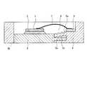
図1は、第1の実施形態における半導体装置の上面図である。また、図2は、図1に示す第1の実施形態における半導体装置をA−A平面で切断した場合の断面図である。<First Embodiment>
FIG. 1 is a top view of the semiconductor device according to the first embodiment. FIG. 2 is a cross-sectional view of the semiconductor device according to the first embodiment shown in FIG. 1 cut along an AA plane.
半導体素子1の下面は、はんだ等の接合部材2によって、通電および放電機能を有する第1のバスバー3に接合されている。第1のバスバー3は、第1の樹脂部5と一体成形されており、枠状の形状をしている。より具体的には、枠状の形状である第1の樹脂部5が第1のバスバー3の外周を覆って第1のバスバー3と一体成形されている。なお、第1のバスバー3と第1の樹脂部5とが一体成形されている必要はない。 The lower surface of the
第1の樹脂部5は、第1の樹脂材で形成されている。第1の樹脂材は、例えば、PPS(ポリフェニレンサルファイド)やPBT(ポリブチレンテレフタート)である。 The
半導体素子1の上面は、アルミからなるボンディングワイヤ7によって、第2のバスバー4に接続されている。半導体素子1は、IGBTやダイオードである。半導体素子1がIGBTの場合、半導体素子の上面側はエミッタ電極、下面側はコレクタ電極である。 The upper surface of the
第1のバスバー3および第2のバスバー4は、電源に接続されている。 The
なお、半導体素子1は、複数並列に接続されていてもよい。 Note that a plurality of
ワイヤボンディングされた半導体装置は、第2の樹脂材であるエポキシ樹脂からなる第2の樹脂部6によって封止される。ただし、第2の樹脂材がエポキシ樹脂に限定されることはない。 The wire bonded semiconductor device is sealed with a
第2の樹脂部6の封止工法としては、第1の樹脂部5からなるケースに大気圧もしくは減圧下で第2の樹脂材を流し込んだ後、高温下で樹脂を硬化させる工法や、キャビティを有する金型内に半導体装置をセットし、圧力をかけながら樹脂をケース内に注入するトランスファーモールド工法を用いることができる。ただし、第2の樹脂部6の封止工法が上述した工法に限定されることはない。 As a sealing method for the
なお、内部構造を分かりやすくするため、図1では、第2の樹脂部6を図示していないが、第1の樹脂部5の上面の高さ以下、もしくは同じ高さまで第2の樹脂部6が充填されている。 In order to make the internal structure easy to understand, the
第1のバスバー3は、例えば銅からなり、その線膨張係数は17ppm/℃である。また、第2の樹脂部6は、線膨張係数が第1のバスバー3よりも小さく、例えば13ppm/℃程度に調整されたエポキシ樹脂である。 The
第1のバスバー3は、図2に示すように、第1の樹脂部5側に延伸した凸部3aを有している。凸部3aの上面および下面はそれぞれ、第1の樹脂部5に接している。第1のバスバー3の凸部3aの上面と第1の樹脂部5との接合面は、第1の樹脂部5と第2の樹脂部6との接合面と略平行である。 As shown in FIG. 2, the
第1のバスバー3の凸部3aの上部において、第2の樹脂部6と接する第1の樹脂部5の接合面は、その表面が粗い粗化面5aを有する。粗化面5aは、例えば、ショットブラストで製作したり、樹脂材の成型金型を粗くすることによって製作することができる。このような構成とすることにより、第1の樹脂部5の粗化面5aと第2の樹脂部6との接合面の接合強度は、第1のバスバー3の凸部3aの上面と第1の樹脂部5との接合面の接合強度よりも大きくなる。 In the upper part of the
ここで、第1の実施形態における半導体装置が高温環境下に置かれると、第1のバスバー3と第2の樹脂部6の線膨張係数の違いから、第1のバスバー3が第2の樹脂部6よりも半導体素子1の外周方向に伸びようとする。 Here, when the semiconductor device according to the first embodiment is placed in a high temperature environment, the
図3は、高温環境下に置かれた半導体装置の第1のバスバー3が膨張した状態を示す図である。図3では、膨張する前の第1のバスバー3の大きさを波線3bで示している。また、以下の説明のため、第1のバスバー3の凸部3aと第2の樹脂部6との間にある第1の樹脂部5の部分を薄肉部5bと呼ぶ。 FIG. 3 is a view showing a state where the
上述したように、第1のバスバー3の凸部3aの上面と第1の樹脂部5の接合面は、第1の樹脂部5と第2の樹脂部6との接合面と略平行であるため、第1のバスバー3の外周方向の変位に対して、両接合面には、同じ方向の応力が発生する。また、第1の樹脂部5の粗化面5aと第2の樹脂部6との接合面の接合強度は、第1のバスバー3の凸部3aの上面と第1の樹脂部5との接合面の接合強度よりも大きい。従って、第1のバスバー3の外周方向の変位に対して、第1の樹脂部5の薄肉部5bと、第1のバスバー3の凸部3aの接合面が剥離して、薄肉部5bが変形する。これにより、第1の樹脂部5の粗化面5aと第2の樹脂部6との接合面に加わるせん断応力を低下させることができ、この接合面が剥離することを防止して、第1のバスバー3と第2のバスバー4間での絶縁信頼性が低下することを防ぐことができる。 As described above, the upper surface of the
また、第1の樹脂部5の粗化面5aと第2の樹脂部6との接合面が剥離することなく、第1のバスバー3と第2のバスバー4との間の絶縁性を確保することができるので、第1のバスバー3と第2のバスバー4間の絶縁距離を小さくすることができる。これにより、絶縁信頼性を確保したまま、半導体装置のサイズを小さくすることができる。 Moreover, the insulation between the 1st bus-
以上、第1の実施形態における半導体装置は、電源に接続されたバスバー3と、バスバー3の表面に載置され、表裏面の電極面のうちの少なくとも一方の電極面がバスバー3に電気的に接続された半導体素子1と、第1の樹脂材で形成され、枠状の形状でバスバー3の外周を覆ってバスバー3と接合する第1の樹脂部5と、第2の樹脂材で形成され、枠状の第1の樹脂部の内部に充填されて半導体素子1をモールドするとともに、第1の樹脂部5およびバスバー3と接合する第2の樹脂部6とを備える。そして、第1の樹脂部5と第2の樹脂部6との接合面の接合強度は、第1の樹脂部5とバスバー3との接合面の接合強度よりも大きい。このような構成としたことにより、半導体装置が熱膨張する際に、相対的に接合強度が小さい第1の樹脂部5とバスバー3との接合面が先に剥離して変形することで、バスバー3と第2の樹脂部6の接合面が剥離するのを防いで、バスバー3と、半導体素子面と同電位の部材との間の絶縁信頼性が低下するのを防ぐことができる。また、第1の樹脂部5と第2の樹脂部6の接合面が剥離した場合を考慮してバスバー3と、半導体素子面と同電位の部材との間の絶縁距離を大きくする必要が無いので、半導体装置を小型化することができる。 As described above, the semiconductor device according to the first embodiment is placed on the
第1の樹脂部5と第2の樹脂部6との接合面は、第1の樹脂部5とバスバー3との接合面と略平行であるので、半導体装置が熱膨張すると、第1の樹脂部5と第2の樹脂部6との接合面には、第1の樹脂部5とバスバー3との接合面と同じ方向の力が加わる。これにより、相対的に強度が小さい第1の樹脂部5とバスバー3との接合面が確実に先に剥離して変形するので、バスバー3と第2の樹脂部6の接合面が剥離して、バスバーと、半導体素子面と同電位の部材との間の絶縁信頼性が低下するのを防ぐことができる。 Since the joint surface between the
また、第1の樹脂部5と第2の樹脂部6との接合面における第1の樹脂部5の少なくとも一部の表面は、第1の樹脂部5とバスバー3との接合面における第1の樹脂部5の表面に比べて粗い。これにより、複雑な工程を追加することなく、第1の樹脂部5と第2の樹脂部6との接合面の接合強度を、第1の樹脂部5とバスバー3との接合面の接合強度よりも大きくすることができる。 Further, at least a part of the surface of the
さらに、バスバー3は、第1の樹脂部5側に突出した凸部3aを有し、凸部3aの上面および下面は、それぞれ第1の樹脂部5と接合している、すなわち、凸部3aは、第1の樹脂部5によって挟み込まれているので、第1の樹脂部5がバスバー3から外れるのを防ぐことができる。 Furthermore, the
<第2の実施形態>
第2の実施形態における半導体装置の構成は、第1の実施形態における半導体装置の構成と同じである。第2の実施形態における半導体装置が第1の実施形態における半導体装置と異なるのは、第1のバスバー3と第2の樹脂部6の線膨張係数の大小関係である。すなわち、第2の実施形態における半導体装置では、第1のバスバー3の線膨張係数よりも、第2の樹脂部6の線膨張係数の方が大きい。ここでは、第1のバスバー3の線膨張係数は、第1の実施形態と同じ(17ppm/℃)とし、第2の樹脂部6の線膨張係数を、20ppm/℃とする。<Second Embodiment>
The configuration of the semiconductor device in the second embodiment is the same as the configuration of the semiconductor device in the first embodiment. The semiconductor device in the second embodiment is different from the semiconductor device in the first embodiment in the magnitude relationship between the linear expansion coefficients of the
第2の実施形態における半導体装置が低温環境下に置かれると、半導体装置全体が熱収縮する。その際に、第1のバスバー3の線膨張係数と第2の樹脂部6の線膨張係数の大小関係から、第1のバスバー3が第2の樹脂部6よりも半導体素子1の内周方向に縮もうとする。 When the semiconductor device according to the second embodiment is placed in a low temperature environment, the entire semiconductor device is thermally contracted. At this time, the
図4は、低温環境下に置かれた半導体装置の第1のバスバー3が収縮した状態を示す図である。図4では、収縮する前の第1のバスバー3の大きさを波線3cで示している。 FIG. 4 is a diagram showing a state where the
第1の実施形態における半導体装置と同様に、第1のバスバー3の凸部3aの上面と第1の樹脂部5の接合面は、第1の樹脂部5と第2の樹脂部6との接合面と略平行である。また、第1の樹脂部5の粗化面5aと第2の樹脂部6との接合面の接合強度は、第1のバスバー3の凸部3aの上面と第1の樹脂部5との接合面の接合強度よりも大きい。従って、第1のバスバー3の内周方向への変位に対して、第1の樹脂部5の薄肉部5bと、第1のバスバー3の凸部3aの接合面が剥離して、薄肉部5bが変形する。これにより、第1の樹脂部5の粗化面5aと第2の樹脂部6との接合面に加わるせん断応力を低下させることができ、この接合面が剥離することを防止することにより、第1のバスバー3と第2のバスバー4間で絶縁信頼性が低下することを防ぐことができる。 Similar to the semiconductor device in the first embodiment, the upper surface of the
また、第1の樹脂部5の粗化面5aと第2の樹脂部6との接合面が剥離することなく、第1のバスバー3と第2のバスバー4との間の絶縁性を確保することができるので、第1のバスバー3と第2のバスバー4間の絶縁距離を小さくすることができる。これにより、絶縁信頼性を確保したまま、半導体装置のサイズを小さくすることができる。 Moreover, the insulation between the 1st bus-
以上、第2の実施形態における半導体装置によれば、半導体装置が熱収縮する場合でも、相対的に強度が小さい第1の樹脂部5とバスバー3との接合面が先に剥離して変形することで、第1の樹脂部5と第2の樹脂部6の接合面が剥離するのを防いで、バスバー3と、半導体素子面と同電位の部材との間の絶縁信頼性が低下するのを防ぐことができる。また、第1の樹脂部5と第2の樹脂部6の接合面が剥離した場合を考慮してバスバー3と、半導体素子面と同電位の部材との間の絶縁距離を大きくする必要が無いので、半導体装置を小型化することができる。 As described above, according to the semiconductor device of the second embodiment, even when the semiconductor device thermally contracts, the joint surface between the
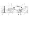
<第3の実施形態>
図5は、第3の実施形態における半導体装置の上面図である。また、図6は、図5に示す第3の実施形態における半導体装置をB−B平面で切断した場合の断面図である。<Third Embodiment>
FIG. 5 is a top view of the semiconductor device according to the third embodiment. FIG. 6 is a cross-sectional view of the semiconductor device according to the third embodiment shown in FIG. 5 taken along the BB plane.
第1および第2の実施形態における半導体装置では、半導体素子1の上面は、ボンディングワイヤ7によって、第2のバスバー4に接続される構成となっていた。第3の実施形態における半導体装置では、半導体素子1の上面は、はんだ等の接合部材8によって、第2のバスバー4に接合されている。すなわち、第3の実施形態における半導体装置は、半導体素子1の両面にバスバー3、4が接続され、半導体素子1によって発生した熱を半導体素子1の両面のバスバー3、4を介して放熱することができる、放熱性の良い両面放熱型半導体装置である。 In the semiconductor device according to the first and second embodiments, the upper surface of the
第3の実施形態における半導体装置において、第1のバスバー3は、第1の樹脂部5側であって、図6の左右方向に延伸した凸部3aを有している。2つの凸部3aの上面および下面はそれぞれ、第1の樹脂部5に接している。第1のバスバー3の凸部3aのそれぞれの上面と第1の樹脂部5との接合面は、第1の樹脂部5と第2の樹脂部6との接合面と略平行である。 In the semiconductor device according to the third embodiment, the
また、2つの凸部3aの上部において、第2の樹脂部6と接する第1の樹脂部5の接合面は、その表面が粗い粗化面5aを有する。このような構成とすることにより、第1の樹脂部5の粗化面5aと第2の樹脂部6との接合面の接合強度は、第1のバスバー3の凸部3aの上面と第1の樹脂部5との接合面の接合強度よりも大きくなる。 In addition, in the upper part of the two
なお、第1のバスバー3と第2の樹脂部6の線膨張係数の大小関係は、第1の実施形態と同じとする。すなわち、第1のバスバー3の線膨張係数よりも、第2の樹脂部6の線膨張係数の方が小さい。 The magnitude relationship between the linear expansion coefficients of the
第3の実施形態における半導体装置が高温環境下に置かれると、第1の実施形態における半導体装置と同様に、第1の樹脂部5の薄肉部5bと、第1のバスバー3の凸部3aの接合面が剥離して、薄肉部5bが変形する。これにより、第1の樹脂部5の粗化面5aと第2の樹脂部6との接合面に加わるせん断応力を低下させることができ、この接合面が剥離することを防止して第1のバスバー3と第2のバスバー4間で絶縁信頼性が低下することを防ぐことができる。 When the semiconductor device according to the third embodiment is placed in a high temperature environment, the
また、第1の樹脂部5の粗化面5aと第2の樹脂部6との接合面が剥離することなく、第1のバスバー3と第2のバスバー4との間の絶縁性を確保することができるので、第1のバスバー3と第2のバスバー4間の絶縁距離を小さくすることができる。これにより、絶縁信頼性を確保したまま、半導体装置のサイズを小さくすることができる。 Moreover, the insulation between the 1st bus-
以上、第3の実施形態における半導体装置によれば、半導体素子1の両面にバスバー3、4を接続する構成であっても、第1の実施形態における半導体装置と同様に、半導体装置が熱膨張する際に、相対的に接合強度が小さい第1の樹脂部5とバスバー3との接合面が先に剥離して変形することで、第1の樹脂部5と第2の樹脂部6の接合面が剥離するのを防いで、バスバー3と、半導体素子面と同電位の部材との間の絶縁信頼性が低下するのを防ぐことができる。また、第1の樹脂部5と第2の樹脂部6の接合面が剥離した場合を考慮してバスバー3と、半導体素子面と同電位の部材との間の絶縁距離を大きくする必要が無いので、半導体装置を小型化することができる。 As described above, according to the semiconductor device in the third embodiment, even when the
<第4の実施形態>
第4の実施形態における半導体装置の構成は、第3の実施形態における半導体装置の構成と同じである。第4の実施形態における半導体装置が第3の実施形態における半導体装置と異なるのは、第1のバスバー3と第2の樹脂部6の線膨張係数の大小関係である。すなわち、第4の実施形態における半導体装置では、第1のバスバー3の線膨張係数よりも、第2の樹脂部6の線膨張係数の方が大きい。ここでは、第1のバスバー3の線膨張係数は、第1の実施形態と同じ(17ppm/℃)とし、第2の樹脂部6の線膨張係数を、20ppm/℃とする。<Fourth Embodiment>
The configuration of the semiconductor device in the fourth embodiment is the same as the configuration of the semiconductor device in the third embodiment. The semiconductor device in the fourth embodiment differs from the semiconductor device in the third embodiment in the magnitude relationship between the linear expansion coefficients of the
第4の実施形態における半導体装置が低温環境下に置かれると、半導体装置全体が熱収縮する。その際に、第1のバスバー3の線膨張係数と第2の樹脂部6の線膨張係数の大小関係から、第1のバスバー3が第2の樹脂部6よりも半導体素子1の外周方向に縮もうとする。 When the semiconductor device according to the fourth embodiment is placed in a low temperature environment, the entire semiconductor device is thermally contracted. At that time, the
第3の実施形態における半導体装置と同様に、第1のバスバー3の凸部3aの上面と第1の樹脂部5の接合面は、第1の樹脂部5と第2の樹脂部6との接合面と略平行である。また、第1の樹脂部5の粗化面5aと第2の樹脂部6との接合面の接合強度は、第1のバスバー3の凸部3aの上面と第1の樹脂部5との接合面の接合強度よりも大きい。従って、第1のバスバー3の外周方向の変位に対して、第1の樹脂部5の薄肉部5bと、第1のバスバー3の凸部3aの接合面が剥離して、薄肉部5bが変形する。これにより、第1の樹脂部5の粗化面5aと第2の樹脂部6との接合面に加わるせん断応力を低下させることができ、この接合面が剥離することを防止して第1のバスバー3と第2のバスバー4間で絶縁信頼性が低下することを防ぐことができる。 Similar to the semiconductor device according to the third embodiment, the upper surface of the
以上、第4の実施形態における半導体装置によれば、半導体素子1の両面にバスバー3、4を接続する構成であっても、第2の実施形態における半導体装置と同様、半導体装置が熱収縮する際に、相対的に接合強度が小さい第1の樹脂部5とバスバー3との接合面が先に剥離して変形することで、第1の樹脂部5と第2の樹脂部6の接合面が剥離するのを防いで、バスバー3と、半導体素子面と同電位の部材との間の絶縁信頼性が低下するのを防ぐことができる。また、第1の樹脂部5と第2の樹脂部6の接合面が剥離した場合を考慮してバスバー3と、半導体素子面と同電位の部材との間の絶縁距離を大きくする必要が無いので、半導体装置を小型化することができる。 As described above, according to the semiconductor device in the fourth embodiment, even when the
本発明は、上述した第1〜第4の実施形態に限定されることはない。例えば、上述した各実施形態では、第2の樹脂部6と接する第1の樹脂部5の接合面は、その表面が粗い粗化面5aを有する構成とすることにより、第1の樹脂部5と第2の樹脂部6との接合面の接合強度を、第1の樹脂部5とバスバー3との接合面の接合強度よりも大きくした。しかしながら、第1の樹脂部5と第2の樹脂部6との接合強度を向上させるような中間材を、第1の樹脂部5と第2の樹脂部6との間に介在させることによって、第1の樹脂部5と第2の樹脂部6との接合面の接合強度を、第1の樹脂部5とバスバー3との接合面の接合強度よりも大きくすることもできる。このような中間材としては、例えば、ポリイミドやポリアミドの樹脂からなる薄膜層がある。 The present invention is not limited to the first to fourth embodiments described above. For example, in each of the above-described embodiments, the
1…半導体素子
2…接合部材
3…第1のバスバー
4…第2のバスバー
5…第1の樹脂部
6…第2の樹脂部
8…接合部材DESCRIPTION OF
Claims (5)
Translated fromJapanese前記バスバーの表面に載置され、表裏面の電極面のうちの少なくとも一方の電極面が前記バスバーに電気的に接続された半導体素子と、
第1の樹脂材で形成され、枠状の形状で前記バスバーの外周を覆って前記バスバーと接合する第1の樹脂部と、
第2の樹脂材で形成され、前記枠状の第1の樹脂部の内部に充填されて前記半導体素子をモールドするとともに、前記第1の樹脂部および前記バスバーと接合する第2の樹脂部と、
を備え、
前記第1の樹脂部と前記第2の樹脂部との接合面の接合強度は、前記第1の樹脂部と前記バスバーとの接合面の接合強度よりも大きい、
ことを特徴とする半導体装置。A busbar connected to the power supply;
A semiconductor element mounted on the surface of the bus bar, wherein at least one of the electrode surfaces of the front and back surfaces is electrically connected to the bus bar;
A first resin part formed of a first resin material and covering the outer periphery of the bus bar in a frame-like shape and joined to the bus bar;
A second resin part formed of a second resin material, filled in the inside of the frame-shaped first resin part to mold the semiconductor element, and joined to the first resin part and the bus bar; ,
With
The bonding strength of the bonding surface between the first resin portion and the second resin portion is greater than the bonding strength of the bonding surface between the first resin portion and the bus bar.
A semiconductor device.
ことを特徴とする請求項1に記載の半導体装置。The joint surface between the first resin portion and the second resin portion is substantially parallel to the joint surface between the first resin portion and the bus bar.
The semiconductor device according to claim 1.
ことを特徴とする請求項1または請求項2に記載の半導体装置。The surface of at least a part of the first resin portion at the joint surface between the first resin portion and the second resin portion is the first surface at the joint surface between the first resin portion and the bus bar. Rough compared to the surface of the resin part,
The semiconductor device according to claim 1, wherein the semiconductor device is a semiconductor device.
前記凸部の上面および下面は、前記第1の樹脂部と接合している、
ことを特徴とする請求項1から請求項3のいずれか一項に記載の半導体装置。The bus bar has a convex portion protruding toward the first resin portion side,
The upper surface and the lower surface of the convex part are joined to the first resin part,
The semiconductor device according to claim 1, wherein the semiconductor device is a semiconductor device.
ことを特徴とする請求項1から請求項4のいずれか一項に記載の半導体装置。The electrode surfaces on the front and back surfaces of the semiconductor element are electrically connected to different bus bars,
The semiconductor device according to claim 1, wherein the semiconductor device is a semiconductor device.
Priority Applications (1)
| Application Number | Priority Date | Filing Date | Title |
|---|---|---|---|
| JP2011273223AJP5857709B2 (en) | 2011-12-14 | 2011-12-14 | Semiconductor device |
Applications Claiming Priority (1)
| Application Number | Priority Date | Filing Date | Title |
|---|---|---|---|
| JP2011273223AJP5857709B2 (en) | 2011-12-14 | 2011-12-14 | Semiconductor device |
Publications (2)
| Publication Number | Publication Date |
|---|---|
| JP2013125825Atrue JP2013125825A (en) | 2013-06-24 |
| JP5857709B2 JP5857709B2 (en) | 2016-02-10 |
Family
ID=48776914
Family Applications (1)
| Application Number | Title | Priority Date | Filing Date |
|---|---|---|---|
| JP2011273223AActiveJP5857709B2 (en) | 2011-12-14 | 2011-12-14 | Semiconductor device |
Country Status (1)
| Country | Link |
|---|---|
| JP (1) | JP5857709B2 (en) |
Cited By (4)
| Publication number | Priority date | Publication date | Assignee | Title |
|---|---|---|---|---|
| JP2015150574A (en)* | 2014-02-13 | 2015-08-24 | 日立金属株式会社 | Ceramic sintered body manufacturing method and ceramic sintered body |
| JP2016139692A (en)* | 2015-01-27 | 2016-08-04 | 三菱電機株式会社 | Semiconductor device |
| CN108367500A (en)* | 2016-01-22 | 2018-08-03 | 株式会社电装 | Resin molding |
| WO2024048508A1 (en)* | 2022-09-02 | 2024-03-07 | 三井化学株式会社 | Polyamide resin composition, metal/resin joined body and method for producing same, bus bar unit, drive unit, and mobile object |
Citations (2)
| Publication number | Priority date | Publication date | Assignee | Title |
|---|---|---|---|---|
| JP2005539386A (en)* | 2002-09-17 | 2005-12-22 | オスラム オプト セミコンダクターズ ゲゼルシャフト ミット ベシュレンクテル ハフツング | Lead frame based housing, surface mountable photoelectric component and manufacturing method |
| JP2007214522A (en)* | 2006-02-10 | 2007-08-23 | Intekkusu Kk | Light source device and illuminator using same |
- 2011
- 2011-12-14JPJP2011273223Apatent/JP5857709B2/enactiveActive
Patent Citations (2)
| Publication number | Priority date | Publication date | Assignee | Title |
|---|---|---|---|---|
| JP2005539386A (en)* | 2002-09-17 | 2005-12-22 | オスラム オプト セミコンダクターズ ゲゼルシャフト ミット ベシュレンクテル ハフツング | Lead frame based housing, surface mountable photoelectric component and manufacturing method |
| JP2007214522A (en)* | 2006-02-10 | 2007-08-23 | Intekkusu Kk | Light source device and illuminator using same |
Cited By (7)
| Publication number | Priority date | Publication date | Assignee | Title |
|---|---|---|---|---|
| JP2015150574A (en)* | 2014-02-13 | 2015-08-24 | 日立金属株式会社 | Ceramic sintered body manufacturing method and ceramic sintered body |
| JP2016139692A (en)* | 2015-01-27 | 2016-08-04 | 三菱電機株式会社 | Semiconductor device |
| CN108367500A (en)* | 2016-01-22 | 2018-08-03 | 株式会社电装 | Resin molding |
| US10446458B2 (en) | 2016-01-22 | 2019-10-15 | Denso Corporation | Resin molded body |
| CN108367500B (en)* | 2016-01-22 | 2020-06-09 | 株式会社电装 | resin molded body |
| WO2024048508A1 (en)* | 2022-09-02 | 2024-03-07 | 三井化学株式会社 | Polyamide resin composition, metal/resin joined body and method for producing same, bus bar unit, drive unit, and mobile object |
| JPWO2024048508A1 (en)* | 2022-09-02 | 2024-03-07 |
Also Published As
| Publication number | Publication date |
|---|---|
| JP5857709B2 (en) | 2016-02-10 |
Similar Documents
| Publication | Publication Date | Title |
|---|---|---|
| TWI404177B (en) | Electric power semiconductor circuit device and method for making same | |
| CN104011853B (en) | Semiconductor device for electric power and manufacturing method thereof | |
| JP5213884B2 (en) | Semiconductor device module | |
| CN103794585B (en) | Semiconductor power converter and manufacture method thereof | |
| JP5859906B2 (en) | Semiconductor device and manufacturing method of semiconductor device | |
| US20140001613A1 (en) | Semiconductor package | |
| CN106716813A (en) | Power conversion device | |
| JP6451257B2 (en) | Semiconductor device | |
| JP5857709B2 (en) | Semiconductor device | |
| CN103378025B (en) | Semiconductor device | |
| WO2018159209A1 (en) | Power semiconductor device | |
| JP2015126119A (en) | Semiconductor device and manufacturing method of semiconductor device | |
| CN111095537A (en) | Semiconductor device and power conversion device provided with same | |
| WO2013118275A1 (en) | Semiconductor device | |
| US20130175703A1 (en) | Semiconductor device and method of manufacturing semiconductor device | |
| JP2016039206A (en) | Semiconductor device manufacturing method and semiconductor device | |
| JP2011129818A (en) | Semiconductor device, and method of producing the same | |
| JP2013197573A (en) | Semiconductor device | |
| CN106165089A (en) | Semiconductor module and driving device equipped with semiconductor module | |
| JP7555262B2 (en) | Electrical circuit and power conversion device | |
| JP6567957B2 (en) | Power semiconductor module manufacturing method | |
| JP2011018736A (en) | Semiconductor device | |
| JP2015076441A5 (en) | ||
| JP4339660B2 (en) | Semiconductor device | |
| CN108885939B (en) | Capacitor and capacitor manufacturing method |
Legal Events
| Date | Code | Title | Description |
|---|---|---|---|
| A621 | Written request for application examination | Free format text:JAPANESE INTERMEDIATE CODE: A621 Effective date:20141029 | |
| A977 | Report on retrieval | Free format text:JAPANESE INTERMEDIATE CODE: A971007 Effective date:20150817 | |
| A131 | Notification of reasons for refusal | Free format text:JAPANESE INTERMEDIATE CODE: A131 Effective date:20150901 | |
| A521 | Written amendment | Free format text:JAPANESE INTERMEDIATE CODE: A523 Effective date:20151028 | |
| TRDD | Decision of grant or rejection written | ||
| A01 | Written decision to grant a patent or to grant a registration (utility model) | Free format text:JAPANESE INTERMEDIATE CODE: A01 Effective date:20151117 | |
| A61 | First payment of annual fees (during grant procedure) | Free format text:JAPANESE INTERMEDIATE CODE: A61 Effective date:20151130 | |
| R151 | Written notification of patent or utility model registration | Ref document number:5857709 Country of ref document:JP Free format text:JAPANESE INTERMEDIATE CODE: R151 |