Movatterモバイル変換


[0]ホーム

URL:


JP2013096731A - Radiographic imaging device - Google Patents

Radiographic imaging device
Download PDF

Info

Publication number
JP2013096731A
JP2013096731AJP2011237109AJP2011237109AJP2013096731AJP 2013096731 AJP2013096731 AJP 2013096731AJP 2011237109 AJP2011237109 AJP 2011237109AJP 2011237109 AJP2011237109 AJP 2011237109AJP 2013096731 AJP2013096731 AJP 2013096731A
Authority
JP
Japan
Prior art keywords
radiation
conversion panel
radiation conversion
reset
image
Prior art date
Legal status (The legal status is an assumption and is not a legal conclusion. Google has not performed a legal analysis and makes no representation as to the accuracy of the status listed.)
Pending
Application number
JP2011237109A
Other languages
Japanese (ja)
Inventor
Yasuyoshi Ota
恭義 大田
Haruyasu Nakatsugawa
晴康 中津川
Naoto Iwakiri
直人 岩切
Koichi Kitano
浩一 北野
Current Assignee (The listed assignees may be inaccurate. Google has not performed a legal analysis and makes no representation or warranty as to the accuracy of the list.)
Fujifilm Corp
Original Assignee
Fujifilm Corp
Priority date (The priority date is an assumption and is not a legal conclusion. Google has not performed a legal analysis and makes no representation as to the accuracy of the date listed.)
Filing date
Publication date
Application filed by Fujifilm CorpfiledCriticalFujifilm Corp
Priority to JP2011237109ApriorityCriticalpatent/JP2013096731A/en
Publication of JP2013096731ApublicationCriticalpatent/JP2013096731A/en
Pendinglegal-statusCriticalCurrent

Links

Images

Classifications

Landscapes

Abstract

Translated fromJapanese

【課題】放射線画像を取得できない状態が発生しないようにリセット処理を実行する。
【解決手段】放射線撮影装置(10)において、一方の放射線変換パネル(28a)は、静止画像又は動画像を取得可能な放射線変換パネルであり、他方の放射線変換パネル(28b)は、動画像を取得可能な放射線変換パネルである。この場合、他方の放射線変換パネル(28b)に対してリセット処理部(28c、30、32、40)がリセット処理を実行可能な時間帯にのみ、一方の放射線変換パネル(28a)は、放射線(16)を静止画像又は動画像に変換する。
【選択図】図1
A reset process is executed so that a state in which a radiation image cannot be acquired does not occur.
In a radiation imaging apparatus (10), one radiation conversion panel (28a) is a radiation conversion panel capable of acquiring a still image or a moving image, and the other radiation conversion panel (28b) is a moving image. It is an obtainable radiation conversion panel. In this case, the radiation conversion panel (28a) is exposed to radiation (only in a time zone in which the reset processing unit (28c, 30, 32, 40) can execute the reset process on the other radiation conversion panel (28b). 16) is converted into a still image or a moving image.
[Selection] Figure 1

Description

Translated fromJapanese

本発明は、放射線を放射線画像に変換可能な放射線変換パネルを有し、該放射線変換パネルに対して残像の発生を抑制するためのリセット処理を実行可能な放射線撮影装置に関する。  The present invention relates to a radiation imaging apparatus having a radiation conversion panel capable of converting radiation into a radiation image and capable of executing a reset process for suppressing the occurrence of an afterimage on the radiation conversion panel.

放射線を放射線画像に変換可能な放射線変換パネルを有する放射線撮影装置において、該放射線変換パネルに対してリセット処理を実行することにより、残像の発生を抑制することが、例えば、特許文献1〜3に開示されている。  In a radiation imaging apparatus having a radiation conversion panel capable of converting radiation into a radiation image, for example, Patent Documents 1 to 3 disclose that after-image generation is suppressed by executing reset processing on the radiation conversion panel. It is disclosed.

なお、放射線撮影装置で取得される放射線画像に対するアーチファクトとしての残像は、温度、駆動時間、バイアスの大きさ、放射線を出力する放射線源の管電圧の大きさによって、放射線変換パネルでの放射線検出に関する応答特性が変化することに起因して発生する。また、放射線を蛍光に変換した後に電荷に変換する間接変換型の放射線変換パネルでは、蛍光を電荷に変換する光電変換素子において、該光電変換素子を構成する半導体の不純物準位(欠陥)に一部の電荷が一旦捕捉され、次回の撮影で、捕捉された前記一部の電荷が、本来の画像情報に応じた電荷と共に出力されることにより、残像が前記画像情報と共に表示装置に表示されてしまう場合もある。さらに、暗電流に起因した電荷も残像の発生原因となる。  The afterimage as an artifact with respect to the radiographic image acquired by the radiographic apparatus relates to the detection of radiation in the radiation conversion panel depending on the temperature, the driving time, the magnitude of the bias, and the magnitude of the tube voltage of the radiation source that outputs the radiation. This occurs due to a change in response characteristics. In addition, in an indirect conversion type radiation conversion panel that converts radiation into fluorescence and then converts it into electric charge, in the photoelectric conversion element that converts fluorescence into electric charge, the impurity level (defect) of the semiconductor constituting the photoelectric conversion element is one. Once the captured charge is captured and the captured partial charge is output together with the charge corresponding to the original image information, the afterimage is displayed on the display device together with the image information. Sometimes it ends up. Furthermore, the charge resulting from the dark current also causes afterimages.

特開2009−5374号公報JP 2009-5374 A特開2010−246835号公報JP 2010-246835 A特開2011−66514号公報JP 2011-66514 A

ところで、放射線撮影装置に対する放射線の照射が繰り返し行われる放射線撮影(動画撮影)においては、ある程度の撮影回数でリセット処理を実行しないと、前述した残像が放射線画像(動画像)に重畳する可能性がある。  By the way, in radiation imaging (moving image capturing) in which radiation irradiation is repeatedly performed on the radiation imaging apparatus, the above-described afterimage may be superimposed on the radiation image (moving image) unless the reset process is performed a certain number of times. is there.

しかしながら、動画撮影のフレームレートが高くなって撮影間隔が短くなると、放射線の非照射時にリセット処理を実行することが困難となり、放射線の照射中にリセット処理を実行せざるを得ない。  However, if the frame rate of moving image shooting is increased and the shooting interval is shortened, it is difficult to execute the reset process when radiation is not irradiated, and the reset process must be performed during radiation irradiation.

上述した特許文献1〜3のリセット処理は、いずれも、放射線変換パネルに蓄積された電荷を読み出してグランドに放出させるというものであり、このようなリセット処理が任意のフレームにおける放射線の照射中に実行されると、該フレームにおいて、所望の動画像を取得できなくなる。  The reset processes of Patent Documents 1 to 3 described above all read out charges accumulated in the radiation conversion panel and discharge them to the ground. Such reset processes are performed during radiation irradiation in an arbitrary frame. When executed, a desired moving image cannot be acquired in the frame.

そのため、例えば、作業者が動画像を見ながら所定の作業を行う場合(例えば、医師が動画像を見ながら患者にカテーテルを挿入する手術を行う場合)に、任意のフレームにおける放射線の照射中にリセット処理が実行されると、次の動画像が取得されるまで、当該作業を中断せざるを得ない。  Therefore, for example, when an operator performs a predetermined operation while watching a moving image (for example, when a doctor performs an operation of inserting a catheter into a patient while watching a moving image), during irradiation of radiation in an arbitrary frame When the reset process is executed, the work must be interrupted until the next moving image is acquired.

本発明は、上記の課題を解消するためになされたものであり、放射線画像を取得できない状態が発生しないようにリセット処理を実行することが可能となる放射線撮影装置を提供することを目的とする。  The present invention has been made to solve the above-described problems, and an object of the present invention is to provide a radiation imaging apparatus that can execute a reset process so that a state in which a radiation image cannot be acquired does not occur. .

上記の目的を達成するために、本発明に係る放射線撮影装置は、放射線の入射方向に沿って積層され、該放射線を放射線画像に変換可能な2つの放射線変換パネルと、前記2つの放射線変換パネルに対して残像の発生を抑制するためのリセット処理を実行可能なリセット処理部とを有し、一方の放射線変換パネルは、静止画像又は動画像を取得可能な放射線変換パネルであると共に、他方の放射線変換パネルは、動画像を取得可能な放射線変換パネルであり、前記他方の放射線変換パネルに対して前記リセット処理部が前記リセット処理を実行可能な時間帯にのみ、前記一方の放射線変換パネルは、前記放射線を前記静止画像又は前記動画像に変換することを特徴としている。  In order to achieve the above object, a radiation imaging apparatus according to the present invention includes two radiation conversion panels that are stacked along a radiation incident direction and that can convert the radiation into a radiation image, and the two radiation conversion panels. A reset processing unit capable of executing a reset process for suppressing the occurrence of an afterimage, and one radiation conversion panel is a radiation conversion panel capable of acquiring a still image or a moving image, and the other The radiation conversion panel is a radiation conversion panel capable of acquiring a moving image, and the one radiation conversion panel is only in a time zone in which the reset processing unit can execute the reset process with respect to the other radiation conversion panel. The radiation is converted into the still image or the moving image.

この構成によれば、前記2つの放射線変換パネルを用いて放射線撮影を行う場合に、前記他方の放射線変換パネルに対するリセット処理中にのみ、前記一方の放射線変換パネルは、静止画撮影又は動画撮影を行うようにしている。このように、本発明は、前記他方の放射線変換パネルが動画撮影を行えない時間帯に、前記一方の放射線変換パネルが静止画撮影又は動画撮影を行うバックアップ機能を備えているため、リセット処理によって放射線画像(動画像又は静止画像)が取得できない状態になることを回避することができる。  According to this configuration, when performing radiation imaging using the two radiation conversion panels, the one radiation conversion panel performs still image capturing or movie capturing only during the reset process for the other radiation conversion panel. Like to do. As described above, the present invention includes a backup function in which the one radiation conversion panel performs still image shooting or movie shooting during a time period when the other radiation conversion panel cannot perform movie shooting. It is possible to avoid a state in which a radiation image (moving image or still image) cannot be acquired.

また、前述のように、前記他方の放射線変換パネルによる動画撮影が行えない時間帯に、前記一方の放射線変換パネルによる静止画撮影又は動画撮影が行われるので、前記放射線撮影装置では、放射線撮影が行えない時間帯は発生しない。そのため、前記放射線を出力する放射線源と前記放射線撮影装置との同期が取れていないことに起因して、前記放射線源が不意に前記放射線を出力した場合であっても、前記放射線撮影装置では、このような突発的な事態に対処して、動画撮影又は静止画撮影を適切に行うことが可能となる。  Further, as described above, since the still image shooting or the moving image shooting by the one radiation conversion panel is performed in the time zone when the moving image shooting by the other radiation conversion panel cannot be performed, the radiography apparatus performs the radiography. There is no time zone that cannot be done. Therefore, because the radiation source that outputs the radiation and the radiation imaging apparatus are not synchronized, even if the radiation source unexpectedly outputs the radiation, the radiation imaging apparatus, In response to such a sudden situation, it is possible to appropriately perform moving image shooting or still image shooting.

さらに、外部の表示装置等に動画像又は静止画像を表示する場合、該表示装置は、通常、前記他方の放射線変換パネルで取得された動画像を表示するが、該他方の放射線変換パネルに対するリセット処理中は、前記一方の放射線変換パネルで取得した静止画像又は動画像を表示することになる。このようにすれば、前記他方の放射線変換パネルに対するリセット処理中に、前記表示装置で画像表示ができなくなることを回避することができる。この結果、前記表示装置に表示された画像を見ながら所定の作業を行っている作業者(例えば、前記画像を見ながら患者にカテーテルを挿入する手術を行っている医師)は、前記作業を中断することなく、該作業を完遂することができる。  Further, when displaying a moving image or a still image on an external display device or the like, the display device usually displays a moving image acquired by the other radiation conversion panel, but resetting the other radiation conversion panel. During processing, a still image or a moving image acquired by the one radiation conversion panel is displayed. In this way, it is possible to avoid that the display device cannot display an image during the reset process for the other radiation conversion panel. As a result, an operator who is performing a predetermined operation while viewing the image displayed on the display device (for example, a doctor performing an operation of inserting a catheter into a patient while viewing the image) interrupts the operation. This work can be completed without doing so.

ここで、前記放射線撮影装置は、前記リセット処理部を制御するリセット制御部をさらに有し、前記リセット制御部は、前記他方の放射線変換パネルが前記動画像を取得可能な時間帯に、前記一方の放射線変換パネルに対するリセット処理を実行するように前記リセット処理部を制御すればよい。  Here, the radiation imaging apparatus further includes a reset control unit that controls the reset processing unit, and the reset control unit includes the one in the time zone in which the other radiation conversion panel can acquire the moving image. What is necessary is just to control the said reset process part so that the reset process with respect to this radiation conversion panel may be performed.

このように、前記他方の放射線変換パネルでの動画撮影中に、前記一方の放射線変換パネルに対するリセット処理を実行すれば、前記一方の放射線変換パネルは、残像の発生が抑制された高画質の静止画像又は前記動画像を取得することができる。なお、前記他方の放射線変換パネルにおいても、前記一方の放射線変換パネルによる静止画撮影又は動画撮影中にリセット処理を実行可能であるため、該他方の放射線変換パネルで取得される動画像についても、残像の発生が抑制された動画像を取得することが可能である。  In this way, if a reset process is performed on the one radiation conversion panel during the moving image shooting on the other radiation conversion panel, the one radiation conversion panel has a high-quality still image in which the occurrence of an afterimage is suppressed. An image or the moving image can be acquired. In the other radiation conversion panel, since the reset process can be executed during still image shooting or moving image shooting by the one radiation conversion panel, the moving image acquired by the other radiation conversion panel is also It is possible to acquire a moving image in which the occurrence of afterimages is suppressed.

また、前記リセット制御部は、前記他方の放射線変換パネルが前記動画像を取得可能な時間帯において、前記放射線の非照射時に、前記他方の放射線変換パネルに対する前記リセット処理よりも短時間の簡易リセット処理を、該他方の放射線変換パネルに対して実行するように前記リセット処理部を制御してもよい。  In addition, the reset control unit can perform a simple reset in a shorter time than the reset process for the other radiation conversion panel when the other radiation conversion panel can acquire the moving image when the radiation is not irradiated. You may control the said reset process part so that a process may be performed with respect to this other radiation conversion panel.

このように、前記放射線の非照射時に短時間の前記簡易リセット処理を実行すれば、前記他方の放射線変換パネルで取得される動画像に残像が重畳することを効果的に抑制することが可能となる。なお、所定のフレームレートで前記放射線の照射が繰り返し行われる場合には、次回の放射線の照射のタイミングを予測することが可能であるため、次のフレームでの動画像の欠落を発生させることなく、前記簡易リセット処理を実行することができる。  As described above, if the simple reset process is performed for a short time when the radiation is not irradiated, it is possible to effectively suppress the afterimage from being superimposed on the moving image acquired by the other radiation conversion panel. Become. In addition, when the radiation irradiation is repeatedly performed at a predetermined frame rate, it is possible to predict the timing of the next radiation irradiation, so that a moving image is not lost in the next frame. The simple reset process can be executed.

上記の各発明において、前記2つの放射線変換パネルは、前記放射線を電荷に変換して蓄積する行列状に配置された複数の画素をそれぞれ有すると共に、画素密度が互いに異なる放射線変換パネルであってもよい。  In each of the above inventions, the two radiation conversion panels may each include a plurality of pixels arranged in a matrix for converting and storing the radiation into electric charges, and having different pixel densities. Good.

これにより、画素密度の低い放射線変換パネルが動画用の前記他方の放射線変換パネルであり、画素密度の高い放射線変換パネルが静止画又は動画用の前記一方の放射線変換パネルであれば、上記の各効果を容易に得ることができる。  Thus, if the radiation conversion panel having a low pixel density is the other radiation conversion panel for moving images and the radiation conversion panel having a high pixel density is the one radiation conversion panel for still images or moving images, The effect can be easily obtained.

このように、画素密度の異なる2つの放射線変換パネルを有する前記放射線撮影装置は、下記[1]〜[5]の特徴を有する。  Thus, the radiation imaging apparatus having two radiation conversion panels having different pixel densities has the following features [1] to [5].

[1] 前記放射線撮影装置では、前記放射線の入射方向に沿って、前記一方の放射線変換パネルである第1の放射線変換パネルと、前記他方の放射線変換パネルである第2の放射線変換パネルとが順に積層され、前記第1の放射線変換パネルは、前記放射線を電荷に直接変換する放射線検出部と、該放射線検出部から電荷を取り出す電荷取出部とを有する直接変換型の放射線変換パネルであり、前記第2の放射線変換パネルは、前記第1の放射線変換パネルを透過した放射線を蛍光に変換するシンチレータと、前記蛍光を電荷に変換する光検出部とを有する間接変換型の放射線変換パネルであればよい。  [1] In the radiation imaging apparatus, a first radiation conversion panel that is the one radiation conversion panel and a second radiation conversion panel that is the other radiation conversion panel are arranged along the incident direction of the radiation. The first radiation conversion panel, which is laminated in order, is a direct conversion type radiation conversion panel having a radiation detection unit that directly converts the radiation into electric charge, and a charge extraction unit that extracts the charge from the radiation detection unit, The second radiation conversion panel may be an indirect conversion type radiation conversion panel having a scintillator that converts the radiation transmitted through the first radiation conversion panel into fluorescence and a light detection unit that converts the fluorescence into electric charge. That's fine.

[2] 上記[1]の場合において、前記シンチレータで放射線から変換された蛍光が前記第1の放射線変換パネルに入射した場合に、該第1の放射線変換パネルは、入射した前記蛍光を電荷に変換可能に構成されていることが好ましい。  [2] In the case of [1] above, when the fluorescence converted from radiation by the scintillator enters the first radiation conversion panel, the first radiation conversion panel converts the incident fluorescence into charges. It is preferably configured to be convertible.

これにより、前記第1の放射線変換パネルは、該第1の放射線変換パネルに照射された放射線を電荷に変換すると共に、前記第2の放射線変換パネルから入射した蛍光も電荷に変換する。この結果、前記第1の放射線変換パネルの感度を高めると共に、該第1の放射線変換パネルにおいて、より高画質の静止画像又は動画像を取得することが可能となる。  As a result, the first radiation conversion panel converts the radiation applied to the first radiation conversion panel into electric charges, and also converts the fluorescence incident from the second radiation conversion panel into electric charges. As a result, it is possible to increase the sensitivity of the first radiation conversion panel and to obtain a still image or moving image with higher image quality in the first radiation conversion panel.

[3] 上記[1]又は[2]の場合において、前記光検出部は、前記蛍光を検出して電荷に変換する光検出素子を含み構成され、前記リセット処理部は、リセット光源又はバイアス電源であり、前記リセット光源から前記光検出素子にリセット光を照射することにより、又は、前記バイアス電源から前記光検出素子へのバイアスの供給を制御することにより、前記光検出素子に対するリセット処理が実行されることが好ましい。  [3] In the case of [1] or [2], the light detection unit includes a light detection element that detects the fluorescence and converts it into a charge, and the reset processing unit includes a reset light source or a bias power source. The reset process for the photodetection element is executed by irradiating the photodetection element with reset light from the reset light source or by controlling the supply of a bias from the bias power source to the photodetection element. It is preferred that

これにより、間接変換型の放射線変換パネルに対して好適なリセット処理を行うことができる。  Thereby, a suitable reset process can be performed with respect to the indirect conversion type radiation conversion panel.

例えば、アモルファスシリコン(a−Si)からなるフォトダイオードが光検出素子である場合、蛍光(可視光)から変換された電荷(電子)の一部がa−Siの不純物準位(欠陥)に一旦捕捉され、その後、動画撮影のような長時間の撮影による前記フォトダイオードの温度上昇等に起因して前記電荷が再放出されると、暗電流等の不要な電流が発生し、放射線画像(動画像)に対するノイズ(残像)の原因となる場合がある。  For example, when a photodiode made of amorphous silicon (a-Si) is a light detection element, a part of charges (electrons) converted from fluorescence (visible light) once enters an a-Si impurity level (defect). When the electric charge is re-emitted due to a temperature rise of the photodiode due to a long time shooting such as moving image shooting, an unnecessary current such as a dark current is generated, and a radiographic image (moving image May cause noise (afterimage).

そこで、前記フォトダイオードに前記リセット光を照射して、前記不純物準位に電荷を予め埋めておき、その後、放射線の照射時に可視光から変換された電荷が前記不純物準位に捕捉されないようにすることで、前記残像の発生を効果的に抑制することができる。  Therefore, the reset light is irradiated to the photodiode to pre-fill the impurity level with charges, and then the charge converted from visible light is not captured by the impurity level when irradiated with radiation. Thus, the occurrence of the afterimage can be effectively suppressed.

[4] 上記[3]の場合において、上述の光検出素子がMIS(Metal−Insulator−Semiconductor)構造のフォトダイオードである場合、前記バイアス電源は、前記フォトダイオードに供給するバイアスの極性を反転するか、又は、前記フォトダイオードへのバイアスの供給を停止することにより、前記フォトダイオードに対するリセット処理を実行することが好ましい。  [4] In the case of [3] above, when the above-described photodetection element is a photodiode having a MIS (Metal-Insulator-Semiconductor) structure, the bias power supply inverts the polarity of the bias supplied to the photodiode. Alternatively, it is preferable to execute reset processing for the photodiode by stopping supply of a bias to the photodiode.

この場合には、前記リセット処理の終了後、次のフレームの動画像を取得するために、前記バイアスの極性を元に戻すか、又は、前記バイアスの供給を再開する処理が必要となるため、前記フォトダイオードが安定した動作状態に復帰するまで多少の時間はかかるが、残像を確実に消去することができる。  In this case, after the reset process is completed, in order to acquire a moving image of the next frame, it is necessary to restore the polarity of the bias or to restart the supply of the bias. Although it takes some time for the photodiode to return to a stable operating state, the afterimage can be reliably erased.

[5] 前記リセット処理部は、前記電荷の蓄積が可能な蓄積状態、又は、蓄積された前記電荷を読み出し可能な読出状態に前記各画素を切り換える駆動回路部と、読出状態の画素から電荷を読み出す読出回路部とであり、前記駆動回路部により前記各画素を前記読出状態に切り換え、前記読出回路部により前記各画素に蓄積された電荷を読み出してグランドに放出させることで、前記各画素に対するリセット処理が実行されてもよい。  [5] The reset processing unit includes: a drive circuit unit that switches the pixels to a storage state in which the charge can be stored or a read state in which the stored charge can be read; and a charge from the pixel in the read state. A readout circuit unit that reads out, and switches each pixel to the readout state by the drive circuit unit, reads out the electric charge accumulated in each pixel by the readout circuit unit, and discharges it to the ground, thereby A reset process may be executed.

このように、前記各画素に蓄積された電荷を読み出して前記グランドに放出するリセット処理を実行する場合でも、該各画素における残像の発生を効果的に抑制することができる。  As described above, even when the reset process for reading out the electric charge accumulated in each pixel and releasing it to the ground is performed, it is possible to effectively suppress the occurrence of an afterimage in each pixel.

このように、(1)各画素(光検出素子)に対するリセット光の照射、(2)各光検出素子に供給されるバイアスの極性の反転、又は、バイアスの供給停止、(3)各画素に蓄積された電荷のグランドへの放出、の3種類のリセット処理のうち、少なくとも1つの処理を行えば、残像の発生を効率よく抑制することができる。なお、前記放射線撮影装置の構成や状態等に応じて、1種類のリセット処理のみ実行したり、又は、複数の種類のリセット処理を使い分けて実行してもよいことは勿論である。  Thus, (1) irradiation of reset light to each pixel (photodetection element), (2) reversal of the polarity of the bias supplied to each photodetection element, or stop supply of bias, (3) to each pixel If at least one of the three types of reset processing of discharging the accumulated charges to the ground is performed, the occurrence of afterimage can be efficiently suppressed. Of course, only one type of reset processing may be executed, or a plurality of types of reset processing may be executed separately according to the configuration and state of the radiation imaging apparatus.

本発明によれば、2つの放射線変換パネルを用いて放射線撮影を行う場合に、他方の放射線変換パネルに対するリセット処理中にのみ、一方の放射線変換パネルは、静止画撮影又は動画撮影を行うようにしている。このように、本発明は、前記他方の放射線変換パネルが動画撮影を行えない時間帯に、前記一方の放射線変換パネルが静止画撮影又は動画撮影を行うバックアップ機能を備えているため、リセット処理によって放射線画像(動画像又は静止画像)が取得できない状態になることを回避することができる。  According to the present invention, when radiation imaging is performed using two radiation conversion panels, only one of the radiation conversion panels performs still image capturing or moving image capturing during the reset process for the other radiation conversion panel. ing. As described above, the present invention includes a backup function in which the one radiation conversion panel performs still image shooting or movie shooting during a time period when the other radiation conversion panel cannot perform movie shooting. It is possible to avoid a state in which a radiation image (moving image or still image) cannot be acquired.

また、前述のように、前記他方の放射線変換パネルによる動画撮影が行えない時間帯に、前記一方の放射線変換パネルによる静止画撮影又は動画撮影が行われるので、放射線撮影装置では、放射線撮影が行えない時間帯は発生しない。そのため、前記放射線を出力する放射線源と前記放射線撮影装置との同期が取れていないことに起因して、前記放射線源が不意に前記放射線を出力した場合であっても、前記放射線撮影装置では、このような突発的な事態に対処して、動画撮影又は静止画撮影を適切に行うことが可能となる。  Further, as described above, since the still image shooting or the moving image shooting by the one radiation conversion panel is performed in the time period in which the moving image shooting by the other radiation conversion panel cannot be performed, the radiation imaging apparatus can perform the radiography. No time zone occurs. Therefore, because the radiation source that outputs the radiation and the radiation imaging apparatus are not synchronized, even if the radiation source unexpectedly outputs the radiation, the radiation imaging apparatus, In response to such a sudden situation, it is possible to appropriately perform moving image shooting or still image shooting.

さらに、外部の表示装置等に動画像又は静止画像を表示する場合、該表示装置は、通常、前記他方の放射線変換パネルで取得された動画像を表示するが、該他方の放射線変換パネルに対するリセット処理中は、前記一方の放射線変換パネルで取得した静止画像又は動画像を表示することになる。このようにすれば、前記他方の放射線変換パネルに対するリセット処理中に、前記表示装置で画像表示ができなくなることを回避することができる。この結果、前記表示装置に表示された画像を見ながら所定の作業を行っている作業者(例えば、前記画像を見ながら患者にカテーテルを挿入する手術を行っている医師)は、前記作業を中断することなく、該作業を完遂することができる。  Further, when displaying a moving image or a still image on an external display device or the like, the display device usually displays a moving image acquired by the other radiation conversion panel, but resetting the other radiation conversion panel. During processing, a still image or a moving image acquired by the one radiation conversion panel is displayed. In this way, it is possible to avoid that the display device cannot display an image during the reset process for the other radiation conversion panel. As a result, an operator who is performing a predetermined operation while viewing the image displayed on the display device (for example, a doctor performing an operation of inserting a catheter into a patient while viewing the image) interrupts the operation. This work can be completed without doing so.

本実施形態に係る放射線撮影装置を有する放射線撮影システムの構成図である。It is a block diagram of the radiography system which has a radiography apparatus which concerns on this embodiment.図1の放射線撮影装置の模式的な回路構成図である。It is a typical circuit block diagram of the radiography apparatus of FIG.図2の放射線検出器における電気的接続を模式的に示す斜視図である。It is a perspective view which shows typically the electrical connection in the radiation detector of FIG.第1の放射線変換パネルの1画素分の電気的接続を示す回路図である。It is a circuit diagram which shows the electrical connection for 1 pixel of a 1st radiation conversion panel.第2の放射線変換パネルの1画素分の電気的接続を示す回路図である。It is a circuit diagram which shows the electrical connection for 1 pixel of a 2nd radiation conversion panel.図1の放射線検出器の概略構成を示す説明図である。It is explanatory drawing which shows schematic structure of the radiation detector of FIG.図6の放射線検出器の1画素分(第1の放射線変換パネルの1画素分及び第2の放射線変換パネルの1画素分)の構成を模式的に示した説明図である。It is explanatory drawing which showed typically the structure for 1 pixel (for 1 pixel of the 1st radiation conversion panel and for 1 pixel of the 2nd radiation conversion panel) of the radiation detector of FIG.図7の1画素分の構成に対する放射線の照射を模式的に示した説明図である。It is explanatory drawing which showed typically irradiation of the radiation | emission with respect to the structure for 1 pixel of FIG.図7の1画素分の構成に対する放射線の照射を模式的に示した説明図である。It is explanatory drawing which showed typically irradiation of the radiation | emission with respect to the structure for 1 pixel of FIG.図7の1画素分の構成に対する放射線の照射を模式的に示した説明図である。It is explanatory drawing which showed typically irradiation of the radiation | emission with respect to the structure for 1 pixel of FIG.放射線の照射、放射線変換パネルでの放射線画像の取得及びリセット処理の実行、並びに、表示装置での表示を示すタイムチャートである。6 is a time chart showing radiation irradiation, acquisition of a radiation image on a radiation conversion panel, execution of a reset process, and display on a display device.

本発明に係る放射線撮影装置について、好適な実施形態を、図1〜図11を参照しながら以下詳細に説明する。  A preferred embodiment of the radiation imaging apparatus according to the present invention will be described in detail below with reference to FIGS.

[本実施形態の構成]
本実施形態に係る放射線撮影装置10を具備する放射線撮影システム12は、図1に示すように、被写体14に対して放射線16を照射する放射線出力装置18と、被写体14を透過した放射線16を検出して放射線画像に変換する放射線撮影装置10と、放射線撮影装置10及び放射線出力装置18を制御するコンソール20と、放射線画像を表示する表示装置22とを備える。
[Configuration of this embodiment]
As shown in FIG. 1, theradiation imaging system 12 including theradiation imaging apparatus 10 according to the present embodiment detects aradiation output device 18 that irradiates the subject 14 withradiation 16 and theradiation 16 that has passed through the subject 14. Theradiation imaging apparatus 10 for converting to a radiation image, theconsole 20 for controlling theradiation imaging apparatus 10 and theradiation output apparatus 18, and thedisplay device 22 for displaying the radiation image are provided.

コンソール20と放射線撮影装置10、放射線出力装置18及び表示装置22との間では、例えば、UWB(Ultra Wide Band)、IEEE802.60.a/b/g/n等の無線LAN(Local Area Network)、又は、ミリ波等を用いた無線通信により信号の送受信が行われる。なお、ケーブルを用いた有線通信により信号の送受信を行ってもよいことは勿論である。  Between theconsole 20, theradiation imaging apparatus 10, theradiation output apparatus 18, and thedisplay apparatus 22, for example, UWB (Ultra Wide Band), IEEE802.60. Signals are transmitted / received by wireless LAN (Local Area Network) such as a / b / g / n or wireless communication using millimeter waves or the like. It goes without saying that signals may be transmitted and received by wired communication using a cable.

コンソール20には、病院内の放射線科において取り扱われる放射線画像やその他の情報を統括的に管理する放射線科情報システム(RIS)24が接続されている。RIS24には、病院内の医事情報を統括的に管理する医事情報システム(HIS)26が接続されている。  Theconsole 20 is connected to a radiology information system (RIS) 24 that comprehensively manages radiographic images and other information handled in the radiology department in the hospital. Connected to theRIS 24 is a medical information system (HIS) 26 that comprehensively manages medical information in the hospital.

本実施形態に係る放射線撮影装置10は、例えば、図示しない撮影台と被写体14との間に配置され、被写体14を透過した放射線16を放射線画像に変換する放射線検出器28を該放射線16を透過可能な筐体内に収容した可搬型の電子カセッテである。  Theradiation imaging apparatus 10 according to the present embodiment is, for example, disposed between an imaging table (not shown) and a subject 14, and transmits theradiation 16 through aradiation detector 28 that converts theradiation 16 that has passed through the subject 14 into a radiation image. It is a portable electronic cassette housed in a possible housing.

放射線撮影装置10は、前述した放射線検出器28と、駆動回路部30を介して放射線検出器28を制御すると共に、放射線検出器28から読出回路部32を介して放射線画像に応じた画像信号(電荷信号、電気信号)を読み出すカセッテ制御部34と、コンソール20との間で信号の送受信を行う通信部36と、放射線撮影装置10内の各部に電力を供給するバッテリ38とを筐体内に収容している。  Theradiation imaging apparatus 10 controls theradiation detector 28 through theradiation detector 28 and thedrive circuit unit 30 described above, and also outputs an image signal (in accordance with the radiation image from theradiation detector 28 through the readout circuit unit 32). Acassette control unit 34 for reading out charge signals and electrical signals), acommunication unit 36 that transmits and receives signals to and from theconsole 20, and abattery 38 that supplies power to each unit in theradiation imaging apparatus 10 are accommodated in the housing. doing.

放射線検出器28は、放射線16の入射方向に沿って、第1の放射線変換パネル(一方の放射線変換パネル)28a、第2の放射線変換パネル(他方の放射線変換パネル)28b、及び、リセット光源28cを順に積層して構成される。なお、本実施形態において、リセット光源28cは、必須ではなく、従って、放射線検出器28は、第1の放射線変換パネル28a及び第2の放射線変換パネル28bとの積層構造を採用することも可能ではあるが、以下の説明では、主として、リセット光源28cを含めた積層構造について説明する。  Theradiation detector 28 includes a first radiation conversion panel (one radiation conversion panel) 28a, a second radiation conversion panel (the other radiation conversion panel) 28b, and a resetlight source 28c along the incident direction of theradiation 16. Are sequentially stacked. In the present embodiment, the resetlight source 28c is not essential. Therefore, theradiation detector 28 may not employ a laminated structure of the firstradiation conversion panel 28a and the secondradiation conversion panel 28b. However, in the following description, a stacked structure including the resetlight source 28c will be mainly described.

第1の放射線変換パネル28aは、主として放射線16の低エネルギー成分を吸収し、吸収したエネルギー成分を電荷に直接変換することにより、該電荷に応じた第1の放射線画像(動画又は静止画)を形成する直接変換型の放射線変換パネルである。第2の放射線変換パネル28bは、主として放射線16の高エネルギー成分を吸収し、吸収したエネルギー成分を蛍光に一旦変換して、変換した蛍光を電荷に変換することにより、該電荷に応じた第2の放射線画像(動画)を形成する間接変換型の放射線変換パネルである。リセット光源28cは、カセッテ制御部34の制御に従って、第2の放射線変換パネル28bにリセット光を照射することにより、残像の発生を抑制するためのリセット処理を実行する。  The firstradiation conversion panel 28a mainly absorbs a low energy component of theradiation 16 and directly converts the absorbed energy component into a charge, thereby generating a first radiation image (moving image or still image) corresponding to the charge. It is a direct conversion type radiation conversion panel to be formed. The secondradiation conversion panel 28b mainly absorbs the high energy component of theradiation 16, temporarily converts the absorbed energy component into fluorescence, and converts the converted fluorescence into electric charge. It is an indirect conversion type radiation conversion panel which forms a radiation image (moving image). The resetlight source 28c executes reset processing for suppressing the occurrence of afterimages by irradiating the secondradiation conversion panel 28b with reset light according to the control of thecassette control unit 34.

なお、放射線16の低エネルギー成分とは、放射線出力装置18を構成する放射線源の管電圧が比較的低電圧である場合での該低電圧に応じた放射線16のエネルギー成分であり、被写体14のマンモ、軟部組織又は腫瘍等に吸収されやすい。また、放射線16の高エネルギー成分とは、放射線源の管電圧が比較的高電圧である場合での該高電圧に応じた放射線16のエネルギー成分であり、被写体14の骨部等に吸収されやすい。  The low energy component of theradiation 16 is an energy component of theradiation 16 corresponding to the low voltage when the tube voltage of the radiation source constituting theradiation output device 18 is relatively low. It is easily absorbed by mammo, soft tissue or tumor. The high energy component of theradiation 16 is an energy component of theradiation 16 corresponding to the high voltage when the tube voltage of the radiation source is relatively high, and is easily absorbed by the bone portion of the subject 14. .

また、放射線撮影装置10には、第1の放射線変換パネル28aにおいて変換された電荷を取り出すために必要な直流電圧を第1の放射線変換パネル28aに供給する電圧供給部42や、第2の放射線変換パネル28bにおいて蛍光を電荷に変換するために必要なバイアス電圧(直流電圧)を第2の放射線変換パネル28bに供給するバイアス電源40も設けられている。  Further, theradiation imaging apparatus 10 includes avoltage supply unit 42 that supplies a DC voltage necessary for taking out the charges converted in the firstradiation conversion panel 28a to the firstradiation conversion panel 28a, and a second radiation. Abias power source 40 is also provided for supplying a bias voltage (DC voltage) necessary for converting fluorescence into electric charge in theconversion panel 28b to the secondradiation conversion panel 28b.

カセッテ制御部34は、放射線検出器28に対する放射線画像の読み出しを指示するためのアドレス信号を駆動回路部30に供給するアドレス信号発生部44と、駆動回路部30の制御によって放射線検出器28から読出回路部32を介して読み出された放射線画像を記憶する画像メモリ46と、放射線撮影装置10を特定するためのカセッテID情報を記憶するカセッテIDメモリ48とを有する。  Thecassette control unit 34 reads an address signal for instructing theradiation detector 28 to read out a radiation image to thedrive circuit unit 30, and reads out from theradiation detector 28 under the control of thedrive circuit unit 30. Animage memory 46 that stores the radiation image read out via thecircuit unit 32 and a cassette ID memory 48 that stores cassette ID information for specifying theradiation imaging apparatus 10 are provided.

また、カセッテ制御部34は、リセット制御部45及び画像処理部47をさらに有する。リセット制御部45は、リセット光源28cを制御するか、バイアス電源40を制御するか、又は、アドレス信号発生部44を介して駆動回路部30及び読出回路部32を制御することにより、第1の放射線変換パネル28a又は第2の放射線変換パネル28bに対する所定のリセット処理を実行させる。従って、リセット光源28c、駆動回路部30、読出回路部32及びバイアス電源40が、第1の放射線変換パネル28a又は第2の放射線変換パネル28bに対するリセット処理を実行可能なリセット処理部として機能する。リセット処理の詳細については後述する。一方、画像処理部47は、放射線検出器28から読出回路部32を介して読み出された、第1の放射線変換パネル28aの放射線画像と第2の放射線変換パネル28bの放射線画像とに対して、加算処理等の所定の画像処理を施す。  Thecassette control unit 34 further includes areset control unit 45 and animage processing unit 47. Thereset control unit 45 controls the resetlight source 28c, thebias power source 40, or thedrive circuit unit 30 and thereadout circuit unit 32 via the addresssignal generation unit 44, thereby A predetermined reset process is performed on theradiation conversion panel 28a or the secondradiation conversion panel 28b. Accordingly, the resetlight source 28c, thedrive circuit unit 30, thereadout circuit unit 32, and thebias power supply 40 function as a reset processing unit that can execute a reset process on the firstradiation conversion panel 28a or the secondradiation conversion panel 28b. Details of the reset process will be described later. On the other hand, theimage processing unit 47 applies the radiation image of the firstradiation conversion panel 28a and the radiation image of the secondradiation conversion panel 28b read out from theradiation detector 28 via thereadout circuit unit 32. Then, predetermined image processing such as addition processing is performed.

コンソール(画像処理装置)20は、通信部50、制御処理部52、オーダ情報記憶部54、撮影条件記憶部56、画像処理部58及び画像メモリ60を有する。  The console (image processing apparatus) 20 includes acommunication unit 50, acontrol processing unit 52, an orderinformation storage unit 54, an imagingcondition storage unit 56, animage processing unit 58, and animage memory 60.

通信部50は、通信部36や、放射線出力装置18、表示装置22及びRIS24との間で信号の送受信を行う。制御処理部52は、コンソール20内の各部を制御するための所定の制御処理を実行する。オーダ情報記憶部54は、被写体14に対する放射線画像の撮影(放射線撮影)を要求するためのオーダ情報を記憶する。撮影条件記憶部56は、被写体14に放射線16を照射させるための撮影条件等を記憶する。画像処理部58は、通信部50が通信部36から受信した放射線画像に対して所定の画像処理(例えば、画像処理部47での加算処理と同様の加算処理)を施す。画像メモリ60は、画像処理部58において画像処理が施された放射線画像等を記憶する。  Thecommunication unit 50 transmits / receives signals to / from thecommunication unit 36, theradiation output device 18, thedisplay device 22, and theRIS 24. Thecontrol processing unit 52 executes predetermined control processing for controlling each unit in theconsole 20. The orderinformation storage unit 54 stores order information for requesting radiographic imaging (radiographic imaging) of the subject 14. The imagingcondition storage unit 56 stores imaging conditions for irradiating the subject 14 with theradiation 16 and the like. Theimage processing unit 58 performs predetermined image processing (for example, addition processing similar to the addition processing in the image processing unit 47) on the radiation image received by thecommunication unit 50 from thecommunication unit 36. Theimage memory 60 stores a radiation image or the like that has been subjected to image processing by theimage processing unit 58.

なお、オーダ情報とは、RIS24又はHIS26において、医師により作成されるものであり、被写体14の氏名、年齢、性別等、被写体14を特定するための被写体情報に加えて、放射線画像の撮影に使用する放射線出力装置18及び放射線撮影装置10の情報や、被写体14の撮影部位及び撮影方法等が含まれる。また、撮影条件とは、例えば、放射線源の管電圧や管電流、放射線16の曝射時間等、被写体14の撮影部位に対して放射線16を照射させるために必要な各種の条件である。  The order information is created by a doctor in theRIS 24 or HIS 26, and is used for radiographic image capturing in addition to subject information for specifying the subject 14, such as the name, age, and sex of the subject 14. Information on theradiation output device 18 and theradiation imaging apparatus 10, the imaging region and imaging method of the subject 14, and the like. The imaging conditions are various conditions necessary for irradiating the imaging region of the subject 14 with theradiation 16 such as the tube voltage and tube current of the radiation source and the exposure time of theradiation 16.

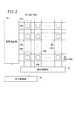
図2は、放射線撮影装置10を構成する放射線検出器28等の模式的な回路構成図である。  FIG. 2 is a schematic circuit configuration diagram of theradiation detector 28 and the like constituting theradiation imaging apparatus 10.

放射線検出器28は、前述のように、放射線16(図1参照)の入射方向に沿って第1の放射線変換パネル28a、第2の放射線変換パネル28b及びリセット光源28cが順に積層された積層構造である。また、放射線検出器28は、図2の平面視では、複数の画素62(62a、62b)がマトリックス状に配列された構造となっている。  As described above, theradiation detector 28 has a stacked structure in which the firstradiation conversion panel 28a, the secondradiation conversion panel 28b, and the resetlight source 28c are sequentially stacked in the incident direction of the radiation 16 (see FIG. 1). It is. Theradiation detector 28 has a structure in which a plurality of pixels 62 (62a, 62b) are arranged in a matrix in the plan view of FIG.

この場合、各画素62は、それぞれ、放射線16の入射方向に沿って、第1の放射線変換パネル28aの一部分(画素62a)と、第2の放射線変換パネル28bの一部分(画素62b)と、リセット光源28cの一部分とを含み構成されている(図1参照)。すなわち、第1の放射線変換パネル28aは、マトリックス状に配列された複数の画素62aを有し、第2の放射線変換パネル28bは、マトリックス状に配列された複数の画素62bを有する。従って、画素62aは、放射線16の低エネルギー成分を電荷に直接変換し、画素62bは、放射線16の高エネルギー成分を蛍光に一旦変換した後に電荷に変換する。リセット光源28cは、各画素62bにリセット光を照射することにより、第2の放射線変換パネル28bに対するリセット処理を実行する。  In this case, eachpixel 62 is reset along a part of the firstradiation conversion panel 28a (pixel 62a) and a part of the secondradiation conversion panel 28b (pixel 62b) along the incident direction of theradiation 16. And a part of thelight source 28c (see FIG. 1). That is, the firstradiation conversion panel 28a has a plurality ofpixels 62a arranged in a matrix, and the secondradiation conversion panel 28b has a plurality ofpixels 62b arranged in a matrix. Accordingly, thepixel 62a directly converts the low energy component of theradiation 16 into electric charge, and thepixel 62b converts the high energy component of theradiation 16 into fluorescent light and then converts it into electric charge. The resetlight source 28c performs a reset process on the secondradiation conversion panel 28b by irradiating eachpixel 62b with reset light.

また、放射線検出器28(の各放射線変換パネル28a、28b)では、行方向と平行に複数のゲート線64a、64bが延びると共に、列方向と平行に複数の信号線66a、66bが延びている。各ゲート線64a、64bは駆動回路部30に接続され、各信号線66a、66bは読出回路部32に接続されている。  In the radiation detector 28 (eachradiation conversion panel 28a, 28b), a plurality ofgate lines 64a, 64b extend in parallel to the row direction, and a plurality ofsignal lines 66a, 66b extend in parallel to the column direction. . The gate lines 64 a and 64 b are connected to thedrive circuit unit 30, and thesignal lines 66 a and 66 b are connected to thereadout circuit unit 32.

図2では、説明の容易化のために、ゲート線64aとゲート線64bとが重ならないように図示すると共に、信号線66aと信号線66bとが重ならないように図示しているが、実際には、図3に示すように、画素62aと画素62b、ゲート線64aとゲート線64b、信号線66aと信号線66bは、互いに重なり合った状態で配置されている。  In FIG. 2, for ease of explanation, thegate line 64a and thegate line 64b are illustrated so as not to overlap with each other, and thesignal line 66a and thesignal line 66b are illustrated not to overlap with each other. As shown in FIG. 3, thepixel 62a and thepixel 62b, thegate line 64a and thegate line 64b, and thesignal line 66a and thesignal line 66b are arranged so as to overlap each other.

具体的に、第1の放射線変換パネル28aでは、行方向に配置された各画素62aに対して、該各画素62aの薄膜トランジスタ(TFT)82a(図4参照)に接続される1本のゲート線64aが配設されると共に、列方向に配置された各画素62aに対して、該各画素62aのTFT82aに接続される1本の信号線66aが配設されている。従って、行列状に複数の画素62aが配置された第1の放射線変換パネル28aには、行数分のゲート線64aと列数分の信号線66aとが配設されている。  Specifically, in the firstradiation conversion panel 28a, for eachpixel 62a arranged in the row direction, one gate line connected to the thin film transistor (TFT) 82a (see FIG. 4) of eachpixel 62a. 64a is arranged, and for eachpixel 62a arranged in the column direction, onesignal line 66a connected to theTFT 82a of eachpixel 62a is arranged. Therefore, in the firstradiation conversion panel 28a in which the plurality ofpixels 62a are arranged in a matrix,gate lines 64a corresponding to the number of rows andsignal lines 66a corresponding to the number of columns are disposed.

第2の放射線変換パネル28bについても、第1の放射線変換パネル28aと同様に、行方向に配置された各画素62bに対して、該各画素62bのTFT82b(図5参照)に接続される1本のゲート線64bが配設されると共に、列方向に配置された各画素62bに対して、該各画素62bのTFT82bに接続される1本の信号線66bが配設されている。そのため、第2の放射線変換パネル28bにおいても、行数分のゲート線64bと列数分の信号線66bとが配設されている。  Similarly to the firstradiation conversion panel 28a, the secondradiation conversion panel 28b is connected to theTFT 82b (see FIG. 5) of eachpixel 62b with respect to eachpixel 62b arranged in the row direction. Onegate line 64b is provided, and onesignal line 66b connected to theTFT 82b of eachpixel 62b is provided for eachpixel 62b arranged in the column direction. Therefore, also in the secondradiation conversion panel 28b,gate lines 64b corresponding to the number of rows andsignal lines 66b corresponding to the number of columns are provided.

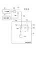
図4及び図5は、1つの画素62a、62bに対する電気的接続をそれぞれ図示したものである。図4及び図5は、画素62a、62bの内部構成が異なる点以外は、概ね同じ構成である。  4 and 5 illustrate electrical connections to onepixel 62a and 62b, respectively. 4 and 5 have substantially the same configuration except that the internal configurations of thepixels 62a and 62b are different.

図4において、画素62aは、第1の放射線検出部72aとTFT82aとを有する。第1の放射線検出部72aは、アモルファスセレン(a−Se)からなる半導体を含み構成され、電圧供給部42とTFT82aとにそれぞれ接続されている。画素62aに放射線16が入射された場合、第1の放射線検出部72aを構成するa−Seの半導体は、入射した放射線16を電荷に直接変換して蓄積する。蓄積された電荷は、電圧供給部42から第1の放射線検出部72aへの直流電圧の供給に起因してTFT82a側に取り出すことができる。  In FIG. 4, thepixel 62a includes a firstradiation detection unit 72a and aTFT 82a. The firstradiation detection unit 72a includes a semiconductor made of amorphous selenium (a-Se), and is connected to thevoltage supply unit 42 and theTFT 82a. When theradiation 16 is incident on thepixel 62a, the a-Se semiconductor constituting the firstradiation detection unit 72a directly converts theincident radiation 16 into an electric charge and accumulates it. The accumulated charge can be taken out to theTFT 82a side due to the supply of the DC voltage from thevoltage supply unit 42 to the firstradiation detection unit 72a.

カセッテ制御部34(図1及び図2参照)のアドレス信号発生部44から駆動回路部30にアドレス信号が供給されると、駆動回路部30からゲート線64aに対して、行方向に配列されたTFT82aをオンオフ制御する制御信号が供給される。TFT82aのオンにより、TFT82aに接続された第1の放射線検出部72aに保持されている電荷がTFT82a及び信号線66aを介して電荷信号として読出回路部32に流出する。  When an address signal is supplied from the addresssignal generation unit 44 of the cassette control unit 34 (see FIGS. 1 and 2) to thedrive circuit unit 30, thedrive circuit unit 30 arranges thegate lines 64a in the row direction. A control signal for ON / OFF control of theTFT 82a is supplied. When theTFT 82a is turned on, the charge held in the firstradiation detection unit 72a connected to theTFT 82a flows out to thereadout circuit unit 32 as a charge signal through theTFT 82a and thesignal line 66a.

読出回路部32は、チャージアンプ110aと、A/D変換器112aとを有する。チャージアンプ110aは、オペアンプ116aと、コンデンサ118aと、スイッチ120aとで構成されている。チャージアンプ110aは、スイッチ120aがオフの場合に、オペアンプ116aに入力された電荷信号を電圧信号に変換し、予め設定されたゲイン、又は、リセット制御部45によって設定されたゲインで電圧信号を増幅し出力する。出力された電圧信号は、A/D変換器112aでA/D変換されてカセッテ制御部34に供給される。  Theread circuit unit 32 includes acharge amplifier 110a and an A /D converter 112a. Thecharge amplifier 110a includes anoperational amplifier 116a, acapacitor 118a, and aswitch 120a. When theswitch 120a is off, thecharge amplifier 110a converts the charge signal input to theoperational amplifier 116a into a voltage signal, and amplifies the voltage signal with a preset gain or a gain set by thereset control unit 45. And output. The output voltage signal is A / D converted by the A /D converter 112 a and supplied to thecassette control unit 34.

ところで、リセット制御部45は、アドレス信号発生部44を介して駆動回路部30及び読出回路部32を制御することにより、第1の放射線変換パネル28aに対するリセット処理を実行させることができる。以下の説明では、リセット制御部45による駆動回路部30及び読出回路部32の制御に起因して実行されるリセット処理を、便宜的に、電気リセット処理ともいう。  By the way, thereset control unit 45 can control thedrive circuit unit 30 and thereadout circuit unit 32 via the addresssignal generation unit 44 to execute a reset process on the firstradiation conversion panel 28a. In the following description, the reset process executed due to the control of thedrive circuit unit 30 and theread circuit unit 32 by thereset control unit 45 is also referred to as an electrical reset process for convenience.

具体的に、第1の放射線変換パネル28aに対する電気リセット処理を実行させる場合、リセット制御部45は、アドレス信号発生部44を制御して駆動回路部30にリセット処理の開始を指示するアドレス信号を供給させることにより、駆動回路部30からゲート線64aに制御信号を供給させてTFT82aをオンさせる。また、リセット制御部45は、アドレス信号発生部44を介して読出回路部32を構成するチャージアンプ110aのスイッチ120aもオンさせる。  Specifically, when the electrical reset process is executed on the firstradiation conversion panel 28a, thereset control unit 45 controls the addresssignal generation unit 44 to send an address signal instructing thedrive circuit unit 30 to start the reset process. By supplying it, a control signal is supplied from thedrive circuit unit 30 to thegate line 64a to turn on theTFT 82a. Thereset control unit 45 also turns on theswitch 120a of thecharge amplifier 110a constituting thereadout circuit unit 32 via the addresssignal generation unit 44.

これにより、コンデンサ118aに蓄積された電荷は、コンデンサ118aとスイッチ120aとの閉回路により放電されると共に、画素62a(を構成する第1の放射線検出部72aの半導体)に蓄積された電荷は、TFT82a、スイッチ120a及びオペアンプ116aを介してグランドに放出される。  Thereby, the electric charge accumulated in thecapacitor 118a is discharged by the closed circuit of thecapacitor 118a and theswitch 120a, and the electric charge accumulated in thepixel 62a (the semiconductor of the firstradiation detection unit 72a constituting) is The light is discharged to the ground through theTFT 82a, theswitch 120a, and theoperational amplifier 116a.

すなわち、温度、駆動時間、直流電圧の大きさ、放射線16を出力する放射線源の管電圧の大きさによって、第1の放射線変換パネル28aでの放射線検出に関する応答特性が変化することに起因して、第1の放射線画像に対するアーチファクトとして残像が発生する場合がある。放射線16が画素62aに照射されていない状態にあっても、画素62aには、暗電流に起因する電荷が蓄積され、残像の発生の原因ともなる。  That is, the response characteristics regarding the radiation detection in the firstradiation conversion panel 28a change depending on the temperature, the driving time, the magnitude of the DC voltage, and the magnitude of the tube voltage of the radiation source that outputs theradiation 16. In some cases, an afterimage may occur as an artifact with respect to the first radiation image. Even in a state where theradiation 16 is not irradiated on thepixel 62a, the charge due to the dark current is accumulated in thepixel 62a, which may cause an afterimage.

そこで、リセット制御部45の制御によってTFT82a及びスイッチ120aをそれぞれオンにし、残像の発生の原因となる電荷をグランドに放出させることにより、該画素62aに対して残像の発生を抑制するための電気リセット処理を行うことができる。なお、電気リセット処理では、画素62aに蓄積された電荷に応じた電圧信号は、A/D変換器112aに出力されずに捨てられることになる。つまり、電気リセット処理により読出回路部32に読み出された電荷信号は、放射線画像を示す画像信号としてカセッテ制御部34に出力されることはない。  Therefore, theTFT 82a and theswitch 120a are turned on under the control of thereset control unit 45, and electric charges that cause the afterimage are discharged to the ground, thereby preventing thepixel 62a from generating afterimages. Processing can be performed. In the electrical reset process, the voltage signal corresponding to the charge accumulated in thepixel 62a is discarded without being output to the A /D converter 112a. That is, the charge signal read to thereadout circuit unit 32 by the electrical reset process is not output to thecassette control unit 34 as an image signal indicating a radiation image.

一方、図5において、画素62bは、第2の放射線検出部72b(図6及び図7参照)であるシンチレータと、フォトダイオード(光検出素子)86bと、TFT82bとを有する。フォトダイオード86bは、アモルファスシリコン(a−Si)等の半導体を含み構成され、バイアス電源40とTFT82bとにそれぞれ接続されている。画素62bに放射線16が入射された場合、画素62bのシンチレータは、放射線16を蛍光に変換し、フォトダイオード86bは、蛍光を電荷に変換して蓄積する。蓄積された電荷は、バイアス電源40からフォトダイオード86bへのバイアス電圧の供給に起因して、TFT82b側に取り出すことができる。  On the other hand, in FIG. 5, thepixel 62 b includes a scintillator that is a secondradiation detection unit 72 b (see FIGS. 6 and 7), a photodiode (light detection element) 86 b, and aTFT 82 b. Thephotodiode 86b includes a semiconductor such as amorphous silicon (a-Si), and is connected to thebias power supply 40 and theTFT 82b. When theradiation 16 is incident on thepixel 62b, the scintillator of thepixel 62b converts theradiation 16 into fluorescence, and thephotodiode 86b converts the fluorescence into electric charge and accumulates it. The accumulated charge can be extracted to theTFT 82b side due to the supply of the bias voltage from thebias power supply 40 to thephotodiode 86b.

アドレス信号発生部44(図1参照)から駆動回路部30へのアドレス信号の供給に起因して、駆動回路部30からゲート線64bに対し、行方向に配列されたTFT82bをオンオフ制御する制御信号が供給されると、TFT82bがオンし、TFT82bに接続されたフォトダイオード86bの電荷が、TFT82b及び信号線66bを介して読出回路部32に流出する。  A control signal for controlling on / off of theTFTs 82b arranged in the row direction from thedrive circuit unit 30 to thegate line 64b due to the supply of the address signal from the address signal generation unit 44 (see FIG. 1) to thedrive circuit unit 30. Is turned on, the charge of thephotodiode 86b connected to theTFT 82b flows out to thereadout circuit portion 32 through theTFT 82b and thesignal line 66b.

読出回路部32は、チャージアンプ110bと、A/D変換器112bとをさらに有する。チャージアンプ110bは、チャージアンプ110aと同様に、オペアンプ116bと、コンデンサ118bと、スイッチ120bとで構成されている。従って、チャージアンプ110bは、スイッチ120bがオフの場合に、オペアンプ116bに入力された電荷信号を電圧信号に変換し、予め設定されたゲイン、又は、リセット制御部45によって設定されたゲインで電圧信号を増幅し出力する。出力された電圧信号は、A/D変換器112bでA/D変換されてカセッテ制御部34に供給される。  Theread circuit unit 32 further includes acharge amplifier 110b and an A /D converter 112b. Similarly to thecharge amplifier 110a, thecharge amplifier 110b includes anoperational amplifier 116b, acapacitor 118b, and aswitch 120b. Therefore, when theswitch 120b is off, thecharge amplifier 110b converts the charge signal input to theoperational amplifier 116b into a voltage signal, and the voltage signal with a preset gain or a gain set by thereset control unit 45. Is amplified and output. The output voltage signal is A / D converted by the A /D converter 112 b and supplied to thecassette control unit 34.

また、第1の放射線変換パネル28aの場合と同様に、第2の放射線変換パネル28bに対しても、電気リセット処理を実行することができる。  Similarly to the case of the firstradiation conversion panel 28a, the electrical reset process can be executed for the secondradiation conversion panel 28b.

この場合、リセット制御部45は、アドレス信号発生部44を制御して駆動回路部30にリセット処理の開始を指示するアドレス信号を供給させることにより、駆動回路部30からゲート線64bに制御信号を供給させてTFT82bをオンさせると共に、アドレス信号発生部44を介してチャージアンプ110bのスイッチ120bもオンさせる。  In this case, thereset control unit 45 controls the addresssignal generation unit 44 to supply an address signal instructing thedrive circuit unit 30 to start the reset process, so that the control signal is sent from thedrive circuit unit 30 to thegate line 64b. Then, theTFT 82b is turned on, and theswitch 120b of thecharge amplifier 110b is also turned on via theaddress signal generator 44.

この結果、コンデンサ118bに蓄積された電荷は、コンデンサ118bとスイッチ120bとの閉回路により放電されると共に、画素62bを構成するフォトダイオード86bに蓄積された電荷は、TFT82b、スイッチ120b及びオペアンプ116bを介してグランドに放出される。  As a result, the charge accumulated in thecapacitor 118b is discharged by the closed circuit of thecapacitor 118b and theswitch 120b, and the charge accumulated in thephotodiode 86b constituting thepixel 62b is passed through theTFT 82b, theswitch 120b, and theoperational amplifier 116b. To the ground.

すなわち、第2の放射線変換パネル28bにおいても、温度、駆動時間、バイアス電圧の大きさ、放射線16を出力する放射線源の管電圧の大きさによって、第2の放射線変換パネル28bでの放射線検出に関する応答特性が変化することに起因して、第2の放射線画像に対するアーチファクトとして残像が発生する場合がある。また、フォトダイオード86bを構成する半導体(例えば、a−Si)の不純物準位(欠陥)に一部の電荷が一旦捕捉され、次回の撮影で、捕捉された一部の電荷が、本来の画像情報に応じた電荷と共に出力されることにより、残像として画像情報と共に表示装置22に表示されてしまう場合もある。さらに、放射線16が画素62bに照射されていない状態では、画素62bには、暗電流に起因した電荷が蓄積され、残像の発生の原因ともなる。  That is, also in the secondradiation conversion panel 28b, the radiation detection in the secondradiation conversion panel 28b depends on the temperature, the driving time, the magnitude of the bias voltage, and the magnitude of the tube voltage of the radiation source that outputs theradiation 16. Due to the change in the response characteristics, an afterimage may occur as an artifact with respect to the second radiation image. Further, some charges are once captured by impurity levels (defects) of the semiconductor (for example, a-Si) constituting thephotodiode 86b, and the captured charges are captured in the next image. By outputting together with the charge corresponding to the information, it may be displayed on thedisplay device 22 together with the image information as an afterimage. Further, in a state where theradiation 16 is not irradiated to thepixel 62b, the charge due to the dark current is accumulated in thepixel 62b, which may cause afterimage.

そこで、リセット制御部45の制御によってTFT82b及びスイッチ120bをそれぞれオンにし、残像の発生の原因となる電荷をグランドに放出させることにより、該画素62bに対しても、残像の発生を抑制するための電気リセット処理を行うことができる。なお、第2の放射線変換パネル28bに対する電気リセット処理においても、画素62bに蓄積された電荷に応じた電圧信号は、A/D変換器112bに出力されずに捨てられることになり、放射線画像を示す画像信号としてカセッテ制御部34に出力されることはない。  Therefore, theTFT 82b and theswitch 120b are turned on under the control of thereset control unit 45, and the charge causing the afterimage is discharged to the ground, thereby suppressing the afterimage from being generated even for thepixel 62b. Electrical reset processing can be performed. Even in the electrical reset processing for the secondradiation conversion panel 28b, the voltage signal corresponding to the electric charge accumulated in thepixel 62b is discarded without being output to the A /D converter 112b, and the radiation image is converted. The image signal is not output to thecassette control unit 34.

ところで、フォトダイオード86bが、MIS構造のフォトダイオードである場合、リセット制御部45は、バイアス電源40を制御してフォトダイオード86bに対するリセット処理を実行させることもできる。以下の説明では、リセット制御部45によるバイアス電源40の制御に起因して実行されるリセット処理を、便宜的に、バイアスリセット処理ともいう。  By the way, when thephotodiode 86b is a MIS structure photodiode, thereset control unit 45 can also control thebias power supply 40 to execute a reset process on thephotodiode 86b. In the following description, the reset process executed due to the control of thebias power supply 40 by thereset control unit 45 is also referred to as a bias reset process for convenience.

バイアスリセット処理において、リセット制御部45は、バイアス電源40からMIS構造のフォトダイオード86bに供給されるバイアス電圧の極性を反転させるか、又は、該フォトダイオード86bへのバイアス電圧の供給を停止させることにより、該フォトダイオード86bに蓄積された電荷を消滅させるか、又は、放出させる。従って、バイアスリセット処理の終了後、リセット制御部45は、バイアス電源40からフォトダイオード86bに供給されるバイアス電圧の極性を元に戻すか、又は、バイアス電圧の供給を再開させる必要がある。なお、このバイアスリセット処理においても、リセット制御部45は、読出回路部32を介してカセッテ制御部34に電圧信号が出力されないように制御する。  In the bias reset process, thereset control unit 45 reverses the polarity of the bias voltage supplied from thebias power supply 40 to thephotodiode 86b having the MIS structure, or stops supplying the bias voltage to thephotodiode 86b. Thus, the charge accumulated in thephotodiode 86b is extinguished or released. Therefore, after the bias reset process is completed, thereset control unit 45 needs to restore the polarity of the bias voltage supplied from thebias power supply 40 to thephotodiode 86b or restart the supply of the bias voltage. In this bias reset process as well, thereset control unit 45 performs control so that a voltage signal is not output to thecassette control unit 34 via thereadout circuit unit 32.

図4及び図5では、1つの画素62a、62bでの電荷の蓄積及び読み出しと、1つの画素62a、62bに対する電気リセット処理と、1つの画素62bに対するバイアスリセット処理とについて説明した。  4 and 5, the charge accumulation and readout in onepixel 62a, 62b, the electrical reset process for onepixel 62a, 62b, and the bias reset process for onepixel 62b have been described.

放射線変換パネル28a、28bは、実際には、図2及び図3に示すように、複数の画素62a、62bが行列状に配置されているため、上述した電荷の蓄積及び読み出しと、電気リセット処理とを、1回のリセット処理において、(1)第1の放射線変換パネル28aの全ての画素62aを対象として行うか、(2)第1の放射線変換パネル28aの一部の(特定の)画素62aを対象として行うか、(3)第2の放射線変換パネル28bの全ての画素62bを対象として行うか、及び/又は、(4)第2の放射線変換パネル28bの一部の(特定の)画素62bを対象として行う。  Theradiation conversion panels 28a and 28b actually have a plurality ofpixels 62a and 62b arranged in a matrix as shown in FIG. 2 and FIG. In one reset process, (1) all thepixels 62a of the firstradiation conversion panel 28a are targeted, or (2) some (specific) pixels of the firstradiationconversion panel 28a 62a, or (3) allpixels 62b of the secondradiation conversion panel 28b, and / or (4) a (specific) part of the secondradiation conversion panel 28b. This is performed for thepixel 62b.

電気リセット処理の場合には、例えば、下記のようにしてリセット処理を行えばよい。すなわち、駆動回路部30及び読出回路部32によるTFT82a、82bのオンオフ制御(各行に対するライン制御)により、各画素62a、62bは、蓄積状態と読出状態とに切り換わることが可能である。そこで、リセット制御部45は、1回の電気リセット処理において、下記(1)〜(5)のようにリセット処理を行えばよい。  In the case of the electrical reset process, for example, the reset process may be performed as follows. That is, each of thepixels 62a and 62b can be switched between the accumulation state and the readout state by the on / off control (line control for each row) of theTFTs 82a and 82b by thedrive circuit unit 30 and thereadout circuit unit 32. Therefore, thereset control unit 45 may perform the reset process as in the following (1) to (5) in one electric reset process.

(1)リセット制御部45は、全てのTFT82a、82bをオンにすることにより、全ての画素62a、62bに対して電気リセット処理を一斉に行えばよい。  (1) Thereset control unit 45 may perform the electrical reset process for all thepixels 62a and 62b at the same time by turning on all theTFTs 82a and 82b.

(2)リセット制御部45は、行毎にTFT82a、82bを順次オンにして、画素62a、62bに対する電気リセット処理を行毎に順次行えばよい。  (2) Thereset control unit 45 may turn on theTFTs 82a and 82b sequentially for each row and sequentially perform the electrical reset processing for thepixels 62a and 62b for each row.

(3)リセット制御部45は、インターレース方式により、奇数行毎又は偶数行毎にTFT82a、82bを順次オンにして、画素62a、62bに対する電気リセット処理を奇数行毎又は偶数行毎に順次行えばよい。  (3) If thereset controller 45 sequentially turns on theTFTs 82a and 82b for each odd row or even row and performs the electrical reset process for thepixels 62a and 62b sequentially for every odd row or even row by the interlace method. Good.

(4)1以上のラインの画素62a、62b(図2及び図3の場合は1以上の行の画素62a、62b)をまとめて1つの領域を形成し、このような領域を前記ラインと直交する方向に複数配置する。そして、リセット制御部45は、それぞれの領域(の画素62a、62b)に対する電気リセット処理を領域毎に順次行えばよい。  (4) One or more lines ofpixels 62a and 62b (in the case of FIGS. 2 and 3, one or more rows ofpixels 62a and 62b) are combined to form one region, and such regions are orthogonal to the lines. Arrange multiple in the direction. Then, thereset control unit 45 may perform the electrical reset process for each region (thepixels 62a and 62b) sequentially for each region.

(5)上記(4)で説明した複数の領域について、リセット制御部45は、インターレース方式により、奇数番の領域毎又は偶数番の領域毎に、それぞれの領域(の画素62a、62b)に対する電気リセット処理を順次行えばよい。  (5) For the plurality of areas described in (4) above, thereset control unit 45 uses the interlace method to generate electricity for each area (pixels 62a and 62b) for each odd-numbered area or even-numbered area. The reset process may be performed sequentially.

なお、以下の説明では、特に断りがない限り、電気リセット処理については、上記(1)又は(2)の方式により行うものとして説明する。  In the following description, unless otherwise specified, the electric reset process is described as being performed by the method (1) or (2).

一方で、バイアスリセット処理と、後述する光リセット処理とについては、全ての画素62a、又は、全ての画素62bを対象として、一斉にリセット処理を行うものとして説明する。  On the other hand, the bias reset process and the light reset process to be described later will be described assuming that the reset process is performed on all thepixels 62a or all thepixels 62b at the same time.

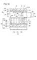
図6は、放射線検出器28の積層構造を模式的に図示したものである。すなわち、図6は、放射線16の入射方向に沿って、表面読取方式としてのISS(Irradiation Side Sampling)方式の直接変換型の第1の放射線変換パネル28a、裏面読取方式としてのPSS(Penetration Side Sampling)方式の間接変換型の第2の放射線変換パネル28b、及び、リセット光源28cを順に積層した構成を図示したものである。  FIG. 6 schematically shows a laminated structure of theradiation detector 28. That is, FIG. 6 shows the firstradiation conversion panel 28a of the direct conversion type of the ISS (Irradiation Side Sampling) method as the surface reading method along the incident direction of theradiation 16, and the PSS (Penetration Side Sampling as the back surface reading method). ) System indirect conversion type secondradiation conversion panel 28b and resetlight source 28c are sequentially stacked.

第1の放射線変換パネル28aは、放射線16の入射方向に沿って、絶縁性基板68aと、第1の電荷検出部(電荷取出部)70aと、第1の放射線検出部72aとを順に積層して構成されている。また、第2の放射線変換パネル28bは、第1の放射線変換パネル28aに向かって(図6の下方向から上方向に向かって)絶縁性基板68bと、第2の電荷検出部(第2の光検出部)70bと、第2の放射線検出部72bとを順に積層して構成されている。  The firstradiation conversion panel 28a sequentially stacks an insulatingsubstrate 68a, a first charge detection unit (charge extraction unit) 70a, and a firstradiation detection unit 72a along the incident direction of theradiation 16. Configured. In addition, the secondradiation conversion panel 28b is directed toward the firstradiation conversion panel 28a (from the lower direction to the upper direction in FIG. 6) and the second charge detection unit (the second charge detection unit). An optical detection unit) 70b and a secondradiation detection unit 72b are sequentially stacked.

絶縁性基板68aは、第1の放射線検出部72a及び第2の放射線検出部72bにおいて放射線16を吸収させるため、放射線16の吸収性が低く、且つ、可撓性を有する電気絶縁性の薄厚の基板(数十μm程度の厚みを有する基板)、具体的には、合成樹脂、アラミド、バイオナノファイバ、あるいは、ロール状に巻き取ることが可能なフイルム状ガラス(超薄板ガラス)等であることが好ましい。  Since the insulatingsubstrate 68a absorbs theradiation 16 in the firstradiation detecting unit 72a and the secondradiation detecting unit 72b, the insulatingsubstrate 68a has a low electric absorption property of theradiation 16 and has a thin and electrically insulating property. A substrate (a substrate having a thickness of about several tens of μm), specifically, a synthetic resin, aramid, bionanofiber, or a film-like glass (ultra-thin glass) that can be wound into a roll. preferable.

第1の放射線検出部72aは、a−Seからなる半導体層74aと、該半導体層74aの第1の電荷検出部70a側の一面に複数形成された画素電極76aと、半導体層74aの他面を全体的に覆うように形成された共通電極78aとから構成される。  Thefirst radiation detector 72a includes asemiconductor layer 74a made of a-Se, a plurality ofpixel electrodes 76a formed on one surface of thesemiconductor layer 74a on thefirst charge detector 70a side, and the other surface of thesemiconductor layer 74a. And acommon electrode 78a formed so as to cover the entire surface.

画素電極76aは、各画素62(62a)毎に形成されており、放射線16に対する吸収性が低く、且つ、a−Seとの間でエレクトロマイグレーションが発生しないような導電性材料(例えば、Au)からなることが好ましい。a−Seの半導体層74aは、放射線16が入射すると、該放射線16の低エネルギー成分を吸収して電荷に変換する。共通電極78aは、第2の放射線検出部72bにおいて放射線16の高エネルギー成分を検出させる一方で、後述するように、第2の放射線変換パネル28bで放射線16から変換された蛍光のうち、少なくともa−Seの感度波長領域の光(例えば、青色波長領域の光)を透過させるために、放射線16の吸収性が低く、a−Seとの間でエレクトロマイグレーションが発生せず、且つ、該感度波長領域の光を透過可能な導電性材料、例えば、ITO(Indium Tin Oxide)からなることが好ましい。  Thepixel electrode 76a is formed for each pixel 62 (62a), has a low absorbability with respect to theradiation 16, and does not generate electromigration with a-Se (for example, Au). Preferably it consists of. When theradiation 16 is incident, thea-Se semiconductor layer 74a absorbs a low energy component of theradiation 16 and converts it into electric charges. While thecommon electrode 78a detects the high energy component of theradiation 16 in the secondradiation detection unit 72b, at least a of the fluorescence converted from theradiation 16 by the secondradiation conversion panel 28b as described later. In order to transmit light in the sensitivity wavelength region of Se (for example, light in the blue wavelength region), the absorption of theradiation 16 is low, electromigration does not occur with a-Se, and the sensitivity wavelength It is preferably made of a conductive material that can transmit light in the region, for example, ITO (Indium Tin Oxide).

なお、画素電極76a及び共通電極78aを形成する場合、形成温度によっては、a−Seが結晶化するおそれがある。従って、a−Seの結晶化を抑制するためには、できる限り低温で画素電極76a及び共通電極78aを形成する必要がある。そこで、画素電極76a及び共通電極78aは、塗布、ロールツーロール、インクジェット等により、金属フィラーを含む有機膜や有機導電体として形成されることが望ましい。  Note that when thepixel electrode 76a and thecommon electrode 78a are formed, a-Se may be crystallized depending on the formation temperature. Therefore, in order to suppress crystallization of a-Se, it is necessary to form thepixel electrode 76a and thecommon electrode 78a at as low a temperature as possible. Therefore, thepixel electrode 76a and thecommon electrode 78a are desirably formed as an organic film or an organic conductor containing a metal filler by coating, roll-to-roll, ink jet, or the like.

第1の電荷検出部70aは、前述したTFT82a(図4及び図7参照)を含み構成され、半導体層74aで発生した電荷を各画素電極76aを介して各画素62a毎に取り出し、取り出した電荷を電気信号(アナログ信号)として信号線66a(図2〜図4参照)を介し読出回路部32に出力する。また、第1の電荷検出部70aは、第1の放射線検出部72a等において放射線16を検出させるため、放射線16の吸収性が低い材料からなることが好ましい。さらに、TFT82aには、ゲート線64a及び信号線66aが接続されるため、これらのゲート線64a及び信号線66aについても、放射線16の吸収性が低く、且つ、低抵抗の導電性材料(例えば、Al)からなることが好ましい。  The firstcharge detection unit 70a is configured to include theTFT 82a (see FIGS. 4 and 7) described above, and the charge generated in thesemiconductor layer 74a is taken out for eachpixel 62a via eachpixel electrode 76a. Is output as an electrical signal (analog signal) to thereadout circuit section 32 via asignal line 66a (see FIGS. 2 to 4). In addition, the firstcharge detection unit 70a is preferably made of a material having low absorption of theradiation 16 so that the firstradiation detection unit 72a and the like detect theradiation 16. Further, since thegate line 64a and thesignal line 66a are connected to theTFT 82a, thegate line 64a and thesignal line 66a also have a low resistance toradiation 16 and a low resistance conductive material (for example, Al) is preferred.

第2の放射線検出部72bは、入射した放射線16の高エネルギー成分を蛍光に変換するシンチレータからなる。シンチレータとしては、a−Seの感度波長領域の光や、第2の電荷検出部70bで吸収可能な波長領域の光(a−Seの感度波長領域の光よりも長波長の光)を発生できるような、比較的広範囲の波長領域を有した蛍光を発生するシンチレータが望ましい。このようなシンチレータとしては、CsI:Na、CaWO、YTaO:Nb、BaFX:Eu(XはBr又はCl)、又は、LaOBr:Tm等があり、特に、CsI:Naがより好ましい。The 2ndradiation detection part 72b consists of a scintillator which converts the high energy component of theincident radiation 16 into fluorescence. As the scintillator, light in the a-Se sensitivity wavelength region or light in a wavelength region that can be absorbed by the secondcharge detection unit 70b (light having a longer wavelength than light in the a-Se sensitivity wavelength region) can be generated. Such a scintillator that generates fluorescence having a relatively wide wavelength range is desirable. Examples of such a scintillator include CsI: Na, CaWO4 , YTaO4 : Nb, BaFX: Eu (X is Br or Cl), LaOBr: Tm, and the like, and CsI: Na is more preferable.

第2の電荷検出部70bは、TFT82b(図5及び図7参照)やフォトダイオード86bを含み構成され、該シンチレータで変換された蛍光を電荷に変換し、変換した電荷を電気信号として信号線66bを介し読出回路部32に出力する。なお、放射線16の低エネルギー成分がa−Seの半導体層74aで吸収されて電荷に変換されると共に、放射線16の高エネルギー成分が第2の放射線検出部72bのシンチレータで吸収されて蛍光に変換されるため、第2の電荷検出部70bのTFT82b及びフォトダイオード86bについては、放射線16の吸収性が低い材料を用いなくてもよい。また、TFT82bに接続されるゲート線64b及び信号線66bについても、放射線16の吸収性が低い導電性材料を用いなくてもよい。  The secondcharge detection unit 70b includes aTFT 82b (see FIGS. 5 and 7) and aphotodiode 86b. The secondcharge detection unit 70b converts the fluorescence converted by the scintillator into a charge, and converts the converted charge into an electric signal as asignal line 66b. Is output to thereadout circuit section 32 via The low energy component of theradiation 16 is absorbed by thea-Se semiconductor layer 74a and converted into electric charges, and the high energy component of theradiation 16 is absorbed by the scintillator of the secondradiation detection unit 72b and converted into fluorescence. Therefore, theTFT 82b and thephotodiode 86b of the secondcharge detection unit 70b may not use a material havinglow radiation 16 absorption. Further, thegate line 64b and thesignal line 66b connected to theTFT 82b may not use a conductive material havinglow radiation 16 absorption.

さらに、放射線16が到達する可能性の低い第2の電荷検出部70bについては、前述したTFT82bとフォトダイオード86bとの組み合わせに代えて、放射線16に対する耐性が低い、CMOS(Complementary Metal−Oxide Semiconductor)イメージセンサ等の他の撮影素子とTFT82bとを組み合わせてもよい。また、TFT82bで言うところのゲート信号に相当するシフトパルスにより電荷をシフトしながら転送するCCD(Charge−Coupled Device)イメージセンサに置き換えることも可能である。  Further, the secondcharge detection unit 70b that is unlikely to reach theradiation 16 is replaced with the combination of theTFT 82b and thephotodiode 86b described above, and has a low resistance to the radiation 16 (CMOS (Complementary Metal-Oxide Semiconductor). Another imaging element such as an image sensor may be combined with theTFT 82b. Further, it can be replaced by a CCD (Charge-Coupled Device) image sensor that transfers charges while shifting the charges by a shift pulse corresponding to the gate signal referred to in theTFT 82b.

絶縁性基板68bは、可撓性を有する電気絶縁性の薄厚の基板であって、且つ、後述するリセット光源28cからのリセット光122cを透過可能であるか、又は、該リセット光122cに対する吸収性や遮光性が低い材料からなることが好ましい。例えば、前述した絶縁性基板68aと同じ材質で絶縁性基板68bを構成してもよい。なお、放射線16が絶縁性基板68bにまで到達する可能性は低いため、該絶縁性基板68bは、放射線16に対する吸収性が低い材料を用いなくてもよい。  The insulatingsubstrate 68b is a thin, electrically insulating and flexible substrate and can transmit reset light 122c from a resetlight source 28c described later, or absorbs thereset light 122c. Or a material having low light shielding properties. For example, the insulatingsubstrate 68b may be made of the same material as the insulatingsubstrate 68a described above. Note that since the possibility that theradiation 16 reaches the insulatingsubstrate 68b is low, the insulatingsubstrate 68b may not use a material having low absorbability with respect to theradiation 16.

リセット光源28cは、エッジライト方式のバックライト光源であり、絶縁性基板68bの底面に導光板124cを配置し、放射線16の非照射領域である導光板124cの側部に冷陰極管126cを配置している。導光板124cと絶縁性基板68bとの間には、第2の電荷検出部70bと対向するように拡散シート128cが介挿されている。リセット光源28cにおける拡散シート128cの箇所以外の外表面には、導光板124c及び冷陰極管126cを囲繞するように反射シート130cも配置されている。  The resetlight source 28c is an edge light type backlight light source, and thelight guide plate 124c is disposed on the bottom surface of the insulatingsubstrate 68b, and thecold cathode tube 126c is disposed on the side of thelight guide plate 124c that is a non-irradiation region of theradiation 16. doing. Adiffusion sheet 128c is interposed between thelight guide plate 124c and the insulatingsubstrate 68b so as to face the secondcharge detection unit 70b. Areflection sheet 130c is also disposed on the outer surface of the resetlight source 28c other than the location of thediffusion sheet 128c so as to surround thelight guide plate 124c and thecold cathode tube 126c.

ここで、リセット制御部45の制御により冷陰極管126cが駆動して、該冷陰極管126cから導光板124cに光が入射すると、導光板124cに入射した前記光は、該導光板124c内部で拡散シート128c及び反射シート130cとの間で表面反射を繰り返した後、該拡散シート128cから絶縁性基板68bにリセット光122cとして出射される。  Here, when thecold cathode tube 126c is driven by the control of thereset control unit 45 and light enters thelight guide plate 124c from thecold cathode tube 126c, the light incident on thelight guide plate 124c is generated inside thelight guide plate 124c. After surface reflection is repeated between thediffusion sheet 128c and thereflection sheet 130c, the light is emitted from thediffusion sheet 128c to the insulatingsubstrate 68b asreset light 122c.

図6では、1本のリセット光122cのみ図示されているが、実際に冷陰極管126cから導光板124cに入射した光は、表面反射を繰り返して導光板124c全体に広がり、拡散シート128cから面発光のリセット光122cとして出射される。従って、バックライト方式のリセット光源28cは、面発光光源として機能し、絶縁性基板68bを介して第2の電荷検出部70bに均一にリセット光122cを照射することになる。これにより、第2の電荷検出部70bを構成する各画素62bのフォトダイオード86bに対して、残像の発生を抑制するためのリセット処理を行うことができる。なお、以下の説明では、リセット制御部45によるリセット光源28cの制御に起因して実行されるリセット処理を、便宜的に、光リセット処理ともいう。  In FIG. 6, only onereset light 122c is shown, but the light that actually enters thelight guide plate 124c from thecold cathode tube 126c repeats surface reflection and spreads over the entirelight guide plate 124c, and the surface from thediffusion sheet 128c. The emitted light is emitted asreset light 122c. Accordingly, the backlight type resetlight source 28c functions as a surface light source, and uniformly irradiates the secondcharge detection unit 70b with thereset light 122c via the insulatingsubstrate 68b. Thereby, a reset process for suppressing the occurrence of afterimages can be performed on thephotodiode 86b of eachpixel 62b constituting the secondcharge detection unit 70b. In the following description, the reset process executed due to the control of the resetlight source 28c by thereset control unit 45 is also referred to as an optical reset process for convenience.

前述のように、例えば、a−Si等からなるフォトダイオード86bの場合、蛍光から変換された電荷(電子)の一部がa−Siの不純物準位(欠陥)に一旦捕捉され、その後、動画撮影のように、長時間の撮影によるフォトダイオード86bの温度上昇等に起因して電荷が再放出されると、暗電流等の不要な電流が発生し、放射線画像に対する残像の原因となる場合がある。  As described above, for example, in the case of thephotodiode 86b made of a-Si or the like, a part of the charge (electrons) converted from the fluorescence is once captured by the impurity level (defect) of the a-Si, and then the moving image When the charge is re-emitted due to the temperature rise of thephotodiode 86b due to long-time shooting as in the case of shooting, unnecessary current such as dark current is generated, which may cause a residual image on the radiographic image. is there.

そこで、光リセット処理を行って、フォトダイオード86bにリセット光122cを照射することにより、不純物準位に電荷を予め埋めておいて、その後、放射線16の照射時に蛍光から変換された電荷が不純物準位に捕捉されないようにすれば、残像の発生を効果的に抑制することができる。  Therefore, an optical reset process is performed to irradiate thephotodiode 86b with thereset light 122c, so that charges are pre-filled in the impurity level. Thereafter, the charge converted from the fluorescence when theradiation 16 is irradiated is converted into the impurity level. If it is prevented from being trapped, the occurrence of afterimages can be effectively suppressed.

なお、図6では、一例として、エッジライト方式のバックライト光源で構成されるリセット光源28cを図示した。リセット光源28cは、これに限定されるものではなく、行列状に配置された画素62bのフォトダイオード86bに対して、確実にリセット光122cを照射して、光リセット処理を実行できるものであればよい。従って、絶縁性基板68bの底面に、第2の電荷検出部70bと対向するように、発光素子のアレイ又はエレクトロルミネッセンス光源を配置することで、リセット光源28cを構成してもよい。  In FIG. 6, as an example, the resetlight source 28 c configured by an edge light type backlight light source is illustrated. The resetlight source 28c is not limited to this, as long as thereset light 122c can be reliably irradiated to thephotodiodes 86b of thepixels 62b arranged in a matrix and the light reset process can be executed. Good. Accordingly, the resetlight source 28c may be configured by arranging an array of light emitting elements or an electroluminescence light source on the bottom surface of the insulatingsubstrate 68b so as to face the secondcharge detection unit 70b.

図7は、図6の放射線検出器28について、1つの画素62(画素62a、62b)に拡大して模式的に図示したものである。  FIG. 7 schematically illustrates theradiation detector 28 of FIG. 6 in an enlarged manner to one pixel 62 (pixels 62a and 62b).

上述のように、1つの画素62は、第1の放射線変換パネル28aの一部分を含む画素62aと、第2の放射線変換パネル28bの一部分を含む画素62bと、リセット光源28cの一部分とから構成されている。  As described above, onepixel 62 includes apixel 62a including a part of the firstradiation conversion panel 28a, apixel 62b including a part of the secondradiation conversion panel 28b, and a part of the resetlight source 28c. ing.

具体的に、1つの画素62aには、第1の放射線検出部72aを構成する1つの画素電極76aが割り当てられている。  Specifically, onepixel electrode 76a configuring the firstradiation detection unit 72a is assigned to onepixel 62a.

また、第1の電荷検出部70aは、絶縁性基板68aの第1の放射線検出部72a側の表面に配設されたTFT82aのアレイを有し、1つの画素62に対して1つのTFT82aが割り当てられている。この場合、絶縁性基板68aにTFT82aのアレイを形成すると、該絶縁性基板68aの第1の放射線検出部72a側は凹凸状となるので、例えば、四フッ化エチレン樹脂膜による平坦化処理を施して平坦化膜84aを形成しておくことが望ましい。  The firstcharge detection unit 70 a has an array ofTFTs 82 a disposed on the surface of the insulatingsubstrate 68 a on the firstradiation detection unit 72 a side, and oneTFT 82 a is assigned to onepixel 62. It has been. In this case, when an array ofTFTs 82a is formed on the insulatingsubstrate 68a, the firstradiation detecting portion 72a side of the insulatingsubstrate 68a becomes uneven, so that, for example, a flattening process using a tetrafluoroethylene resin film is performed. It is desirable to form theplanarizing film 84a.

ゲート線64a及び信号線66a(図2〜図4参照)に接続されるTFT82aは、TFTアレイでの放射線16の吸収を抑制するために、a−Si、アモルファス酸化物(例えば、a−IGZO(InGaZnO))、有機半導体材料、カーボンナノチューブ等からなる活性層を含み構成されることが好ましい。TheTFT 82a connected to thegate line 64a and thesignal line 66a (see FIGS. 2 to 4) has an a-Si, amorphous oxide (e.g., a-IGZO (for example) in order to suppress absorption of theradiation 16 in the TFT array. InGaZnO4 )), an organic semiconductor material, and an active layer made of carbon nanotubes are preferably included.

この場合、a−Siは、300℃程度の基板温度で成膜する必要があるため、ガラス基板を絶縁性基板68aとして用いることになる。これに対して、a−IGZOや有機半導体は、200℃程度の基板温度の低温プロセスにより成膜することが可能であるため、ポリイミド、アラミド等の樹脂基板を絶縁性基板68aとして用いることができ、この結果、可撓性を有するTFTアレイを実現することができる。  In this case, since a-Si needs to be formed at a substrate temperature of about 300 ° C., a glass substrate is used as the insulatingsubstrate 68a. On the other hand, since a-IGZO and organic semiconductor can be formed by a low temperature process at a substrate temperature of about 200 ° C., a resin substrate such as polyimide or aramid can be used as the insulatingsubstrate 68a. As a result, a flexible TFT array can be realized.

画素電極76a及び共通電極78aは、電圧供給部42と電気的に接続されている。  Thepixel electrode 76a and thecommon electrode 78a are electrically connected to thevoltage supply unit 42.

一方、第2の電荷検出部70bは、絶縁性基板68bの第2の放射線検出部72b側の表面に配設されたTFT82b及びフォトダイオード86bのアレイを有し、1つの画素62bに対して1つのTFT82bと1つのフォトダイオード86bとが割り当てられている。この場合も、絶縁性基板68bにTFT82b及びフォトダイオード86bのアレイを形成すると、該絶縁性基板68bの第2の放射線検出部72b側は凹凸状となるので、平坦化膜84aと同様の平坦化膜84bを形成しておくことが望ましい。  On the other hand, the secondcharge detection unit 70b has an array ofTFTs 82b andphotodiodes 86b disposed on the surface of the insulatingsubstrate 68b on the secondradiation detection unit 72b side, and one for onepixel 62b. OneTFT 82b and onephotodiode 86b are allocated. Also in this case, when the array of theTFTs 82b and thephotodiodes 86b is formed on the insulatingsubstrate 68b, thesecond radiation detector 72b side of the insulatingsubstrate 68b becomes uneven, so that the same planarization as theplanarizing film 84a is performed. It is desirable to form the film 84b.

ゲート線64b及び信号線66bに接続されるTFT82bは、TFT82aと同様の活性層を含み構成されることが好ましい。  TheTFT 82b connected to thegate line 64b and thesignal line 66b preferably includes an active layer similar to theTFT 82a.

さらに、図7では、第2の放射線検出部72bとして、CsI:Na(ナトリウム賦活ヨウ化セシウム)のシンチレータを図示している。CsI:Naのシンチレータは、CsI:Naを真空蒸着法で短冊状の柱状結晶構造88bとして形成したものであり、シンチレータの平坦化膜84b側の基端部分は、非柱状結晶部分90bとされ、平坦化膜84bと密着している。非柱状結晶部分90bを設けることにより、第2の放射線検出部72bのシンチレータと、第2の電荷検出部70b及び絶縁性基板68bとの密着性を高めることができる。また、非柱状結晶部分90bの空隙率を0%に近づけたり、(例えば、10μm程度にまで)その厚みを薄くすることにより、後述する蛍光98(図8〜図10参照)の反射を抑えることができる。  Further, in FIG. 7, a scintillator of CsI: Na (sodium-activated cesium iodide) is illustrated as the secondradiation detection unit 72b. The CsI: Na scintillator is formed by forming CsI: Na as a strip-like columnar crystal structure 88b by a vacuum evaporation method, and the base end portion of the scintillator on the flattened film 84b side is anon-columnar crystal portion 90b. It is in close contact with the planarizing film 84b. By providing thenon-columnar crystal portion 90b, the adhesion between the scintillator of the secondradiation detection unit 72b and the secondcharge detection unit 70b and the insulatingsubstrate 68b can be improved. Further, by reducing the porosity of thenon-columnar crystal portion 90b to 0% or reducing its thickness (for example, up to about 10 μm), reflection of fluorescence 98 (see FIGS. 8 to 10) described later is suppressed. Can do.

柱状結晶構造88bを構成する各柱は、放射線16の入射方向に沿ってそれぞれ形成され、隣接する各柱の間には、ある程度の隙間が確保されている。また、CsI:Naのシンチレータは、柱状結晶構造88bが湿度に弱く、非柱状結晶部分90bが湿度に特に弱いという特性を有するので、ポリパラキシリレン樹脂からなる光透過性の防湿保護材92bで封止されている。そして、シンチレータが防湿保護材92bで封止された状態で、柱状結晶構造88bの先端部分と共通電極78aとが密着されている。  Each column constituting the columnar crystal structure 88b is formed along the incident direction of theradiation 16, and a certain gap is secured between adjacent columns. The CsI: Na scintillator has a characteristic that the columnar crystal structure 88b is weak against humidity and thenon-columnar crystal portion 90b is particularly vulnerable to humidity. Therefore, the CsI: Na scintillator is a light-transmitting moistureproofprotective material 92b made of polyparaxylylene resin. It is sealed. And the tip part of the columnar crystal structure 88b and thecommon electrode 78a are in close contact with the scintillator sealed with the moisture-proofprotective material 92b.

このように、a−Seの半導体層74aを含む第1の放射線変換パネル28aと、CsI:Naの柱状結晶構造88bのシンチレータを含む第2の放射線変換パネル28bと、リセット光源28cとの積層構造からなる、放射線検出器28において、図8に示すように、放射線16が入射すると、先ず、a−Seの半導体層74aは、放射線16の低エネルギー成分を吸収して、正電荷94a及び負電荷96aの電荷対に変換する。  Thus, a stacked structure of the firstradiation conversion panel 28a including thea-Se semiconductor layer 74a, the secondradiation conversion panel 28b including the scintillator of the columnar crystal structure 88b of CsI: Na, and the resetlight source 28c. As shown in FIG. 8, whenradiation 16 is incident on theradiation detector 28, thea-Se semiconductor layer 74 a first absorbs the low-energy component of theradiation 16, and causes apositive charge 94 a and a negative charge. Convert to 96a charge pairs.

また、a−Seの半導体層74aで吸収されなかった放射線16(の高エネルギー成分)は、共通電極78aを透過して第2の放射線検出部72bに到達する。  The radiation 16 (high energy component) that has not been absorbed by thea-Se semiconductor layer 74a passes through thecommon electrode 78a and reaches the secondradiation detection unit 72b.

第2の放射線検出部72bでは、柱状結晶構造88b(の発光箇所100)で放射線16の高エネルギー成分を吸収して蛍光98に変換する。発光箇所100で発生した蛍光98の一部(フォトダイオード86bの感度波長領域の光であって、例えば、500nm以上の長波長領域の光)は、放射線16の入射方向に略平行に形成された柱状結晶を直線的に伝播して(直進して)フォトダイオード86bに至り、該フォトダイオード86bは、蛍光98の一部を電荷に変換して蓄積する。  In the secondradiation detection unit 72 b, the columnar crystal structure 88 b (the light emission portion 100) absorbs the high energy component of theradiation 16 and converts it intofluorescence 98. A part of thefluorescence 98 generated at the light emitting portion 100 (light in the sensitivity wavelength region of thephotodiode 86b, for example, light in the long wavelength region of 500 nm or more) was formed substantially parallel to the incident direction of theradiation 16. The columnar crystal propagates linearly (goes straight) to thephotodiode 86b, and thephotodiode 86b converts a part of thefluorescence 98 into electric charge and accumulates it.

また、発光箇所100で発生した蛍光98の他の一部は、共通電極78aの方向に向かって柱状結晶を直進し、透過光102として、ITO等の透明電極からなる共通電極78aを透過し、a−Seの半導体層74aに至る。透過光102がa−Seの感度波長領域の光(例えば、500nm以下の短波長領域の光)であれば、半導体層74aは、透過光102を吸収して正電荷94b及び負電荷96bの電荷対に変換する。  In addition, another part of thefluorescence 98 generated at thelight emitting portion 100 travels straight through the columnar crystal in the direction of thecommon electrode 78a, and passes through thecommon electrode 78a made of a transparent electrode such as ITO as transmittedlight 102. Thesemiconductor layer 74a of a-Se is reached. If the transmittedlight 102 is light in the sensitivity wavelength region of a-Se (for example, light in a short wavelength region of 500 nm or less), thesemiconductor layer 74a absorbs the transmittedlight 102 and haspositive charges 94b andnegative charges 96b. Convert to pair.

各画素電極76a及び共通電極78aには、電圧供給部42の直流電源106及びスイッチ108が電気的に接続されている。ここで、スイッチ108をオンにして、各画素電極76aが正極性、共通電極78aが負極性となるような直流電圧を直流電源106から印加すると、半導体層74aに直流電界が発生する。この直流電界に従って、正電荷94a、94bは、負極性の共通電極78a側に移動すると共に、負電荷96a、96bは、正極性の各画素電極76a側に移動する。この結果、第1の電荷検出部70aは、各画素電極76aを介して負電荷96a、96bを取り出すことが可能となり、駆動回路部30からの制御信号によってTFT82aがオンすると、信号線66aを介して負電荷96a、96bに応じた電気信号を読出回路部32に出力することが可能となる。  TheDC power supply 106 and theswitch 108 of thevoltage supply unit 42 are electrically connected to eachpixel electrode 76a and thecommon electrode 78a. Here, when theswitch 108 is turned on and a DC voltage is applied from theDC power source 106 such that eachpixel electrode 76a has a positive polarity and thecommon electrode 78a has a negative polarity, a DC electric field is generated in thesemiconductor layer 74a. According to this DC electric field, thepositive charges 94a and 94b move to the negativecommon electrode 78a side, and thenegative charges 96a and 96b move to thepositive pixel electrode 76a side. As a result, the firstcharge detection unit 70a can take out thenegative charges 96a and 96b through thepixel electrodes 76a. When theTFT 82a is turned on by the control signal from thedrive circuit unit 30, the firstcharge detection unit 70a passes through thesignal line 66a. Thus, an electrical signal corresponding to thenegative charges 96a and 96b can be output to thereadout circuit section 32.

また、半導体層74a内でアバランシェ効果が発生する程度の直流電圧が各画素電極76aと共通電極78aとの間に印加されると、該アバランシェ効果によって、半導体層74a内の正電荷94a、94b及び負電荷96a、96bが増幅される。この結果、各画素電極76aを介して第1の電荷検出部70a(のTFT82a)で取り出される電荷数を増大させることができる。  Further, when a DC voltage that causes an avalanche effect in thesemiconductor layer 74a is applied between eachpixel electrode 76a and thecommon electrode 78a, thepositive charges 94a, 94b andNegative charges 96a and 96b are amplified. As a result, the number of charges taken out by thefirst charge detector 70a (theTFT 82a) via eachpixel electrode 76a can be increased.

なお、図8では、各画素電極76aが正極性、共通電極78aが負極性となるように、直流電圧を印加した場合を図示しているが、各画素電極76aに負極性及び共通電極78aに正極性の直流電圧を印加した場合でも、上記の効果が得られることは勿論である。  In FIG. 8, a case where a DC voltage is applied so that eachpixel electrode 76a has a positive polarity and thecommon electrode 78a has a negative polarity is illustrated. However, eachpixel electrode 76a has a negative polarity and acommon electrode 78a. Of course, the above effect can be obtained even when a positive DC voltage is applied.

また、上記の説明では、発光箇所100から共通電極78aに向かって柱状結晶構造88bを直進する蛍光98が、該共通電極78aをそのまま透過して透過光102として半導体層74aに入射する場合について説明した。実際には、共通電極78aに向かって直進する蛍光98の一部は、共通電極78aと柱状結晶構造88bとの界面で第2の電荷検出部70b側に反射し、反射光104として第2の電荷検出部70bに向かって柱状結晶構造88bを直進し、フォトダイオード86bに至る。従って、フォトダイオード86bは、入射した反射光104も電荷に変換して蓄積することができる。  Further, in the above description, the case where thefluorescence 98 that goes straight through the columnar crystal structure 88b from thelight emitting portion 100 toward thecommon electrode 78a passes through thecommon electrode 78a as it is and enters thesemiconductor layer 74a as transmitted light 102 is described. did. Actually, part of thefluorescence 98 that goes straight toward thecommon electrode 78 a is reflected toward the secondcharge detection unit 70 b at the interface between thecommon electrode 78 a and the columnar crystal structure 88 b, and is reflected as thesecond light 104. The columnar crystal structure 88b goes straight toward thecharge detection unit 70b and reaches thephotodiode 86b. Therefore, thephotodiode 86b can also convert the incident reflected light 104 into charges and store it.

また、共通電極78aは、500nm以下の短波長領域の蛍光98を透過光102として透過させ、一方で、500nmよりも長波長領域の蛍光98を反射光104として反射させるダイクロイックフィルタとして機能してもよい。あるいは、共通電極78aと柱状結晶構造88bとの間に、このような機能を奏するダイクロイックフィルタを介挿させてもよい。  Thecommon electrode 78a also functions as a dichroic filter that transmits thefluorescence 98 in the short wavelength region of 500 nm or less as the transmittedlight 102 and reflects thefluorescence 98 in the long wavelength region longer than 500 nm as the reflectedlight 104. Good. Alternatively, a dichroic filter having such a function may be interposed between thecommon electrode 78a and the columnar crystal structure 88b.

そして、上述した本実施形態に係る放射線撮影装置10では、静止画撮影又は動画撮影用の画素密度の高い第1の放射線変換パネル28aと、動画撮影用の画素密度の低い第2の放射線変換パネル28bとを有しており、第1の放射線変換パネル28aにおいて高画質の第1の放射線画像を取得し、第2の放射線変換パネル28bにおいて動画像の第2の放射線画像を取得する。  In theradiation imaging apparatus 10 according to this embodiment described above, the firstradiation conversion panel 28a having a high pixel density for still image shooting or movie shooting and the second radiation conversion panel having a low pixel density for movie shooting. 28b, the firstradiation conversion panel 28a acquires a high-quality first radiation image, and the secondradiation conversion panel 28b acquires a moving image second radiation image.

本実施形態では、被写体14に対する動画撮影(被写体14に対して放射線16を繰り返し照射する放射線撮影)において、通常は、第2の放射線変換パネル28bを用いて動画像を取得し、取得した動画像を表示装置22に表示する。また、第2の放射線変換パネル28bに対してリセット処理を行う時間帯においては、第2の放射線画像(動画像)を取得して表示装置22に表示することができないため、このような場合には、第1の放射線変換パネル28aを用いて静止画像又は動画像を取得し、取得した静止画像又は動画像を表示装置22に表示する。  In the present embodiment, in moving image shooting for the subject 14 (radiography for repeatedly irradiating the subject 14 with radiation 16), usually, a moving image is acquired using the secondradiation conversion panel 28b, and the acquired moving image is acquired. Is displayed on thedisplay device 22. In addition, in the case where the second radiation image (moving image) cannot be acquired and displayed on thedisplay device 22 in the time zone in which the reset process is performed on the secondradiation conversion panel 28b, in such a case. Acquires a still image or a moving image using the firstradiation conversion panel 28 a and displays the acquired still image or moving image on thedisplay device 22.

従って、本実施形態では、第1の放射線変換パネル28aと、第2の放射線変換パネル28bとは、互いに異なる時間帯に放射線撮影で使用され、第1の放射線変換パネル28aは、第2の放射線変換パネル28bに対するバックアップ用のパネルとして機能する。つまり、第1の放射線変換パネル28aは、第2の放射線変換パネル28bに対するリセット処理が可能な時間帯にのみ静止画撮影又は動画撮影用のパネルとして使用され、該第1の放射線変換パネル28aに対するリセット処理は、第2の放射線変換パネル28bが動画撮影用のパネルとして使用されている時間帯(第2の放射線画像が取得可能な時間帯)のみに実行される。  Therefore, in the present embodiment, the firstradiation conversion panel 28a and the secondradiation conversion panel 28b are used for radiography in different time zones, and the firstradiation conversion panel 28a is used for the second radiation. It functions as a backup panel for theconversion panel 28b. In other words, the firstradiation conversion panel 28a is used as a still image capturing or moving image capturing panel only during a time period in which the reset processing for the secondradiation conversion panel 28b is possible, and the firstradiation conversion panel 28a The reset process is executed only in a time zone in which the secondradiation conversion panel 28b is used as a moving image capturing panel (a time zone in which the second radiation image can be acquired).

なお、放射線撮影装置10で実行可能なリセット処理としては、前述のように、電気リセット処理、バイアスリセット処理、及び、光リセット処理の3種類のリセット処理がある。このうち、直接変換型の第1の放射線変換パネル28aに対しては、電気リセット処理を実行することが可能である。また、間接変換型の第2の放射線変換パネル28bに対しては、電気リセット処理、バイアスリセット処理、又は、光リセット処理のいずれかのリセット処理を実行することが可能である。  As described above, the reset process that can be executed by theradiation imaging apparatus 10 includes three types of reset processes, that is, an electrical reset process, a bias reset process, and a light reset process. Among these, it is possible to execute an electrical reset process for the direct conversion type firstradiation conversion panel 28a. Moreover, it is possible to perform any reset process of an electrical reset process, a bias reset process, or an optical reset process for the indirect conversion type secondradiation conversion panel 28b.

そして、上述したリセット処理を実行するタイミング及び時間帯については、全て、リセット制御部45で決定され制御される。従って、リセット制御部45は、2つの放射線変換パネル28a、28bに対するリセット処理が上述のように行われるように、リセット光源28c、駆動回路部30、読出回路部32及びバイアス電源40を制御することにより、各放射線変換パネル28a、28bに対する所望のリセット処理を実行させる。  The timing and time zone for executing the reset process described above are all determined and controlled by thereset control unit 45. Accordingly, thereset control unit 45 controls the resetlight source 28c, thedrive circuit unit 30, thereadout circuit unit 32, and thebias power supply 40 so that the reset process for the tworadiation conversion panels 28a and 28b is performed as described above. Thus, a desired reset process is performed on each of theradiation conversion panels 28a and 28b.

図7〜図10には、放射線16の照射中、又は、放射線16の非照射時での放射線変換パネル28a、28bに対するリセット処理も図示されている。  7 to 10 also show reset processing for theradiation conversion panels 28a and 28b during irradiation of theradiation 16 or when theradiation 16 is not irradiated.

図7は、放射線16の非照射時における放射線検出器28の状態を図示している。  FIG. 7 illustrates a state of theradiation detector 28 when theradiation 16 is not irradiated.

ここで、第1の放射線変換パネル28aに対して電気リセット処理を実行する場合には、図4でも説明したように、TFT82a及びスイッチ120aをオンにすればよい。これにより、半導体層74aに蓄積された電荷(暗電流による電荷)を、TFT82a、スイッチ120a及びオペアンプ116aを介してグランドに放出させることができる。  Here, when the electrical reset process is performed on the firstradiation conversion panel 28a, theTFT 82a and theswitch 120a may be turned on as described with reference to FIG. As a result, charges accumulated in thesemiconductor layer 74a (charges due to dark current) can be discharged to the ground via theTFT 82a, theswitch 120a, and theoperational amplifier 116a.

また、第2の放射線変換パネル28bに対してリセット処理を実行する場合には、図5でも説明したように、TFT82b及びスイッチ120bをオンにすればよい。これにより、フォトダイオード86bに蓄積された電荷(暗電流による電荷)を、TFT82b、スイッチ120b及びオペアンプ116bを介してグランドに放出させることができる。  Further, when the reset process is executed on the secondradiation conversion panel 28b, theTFT 82b and theswitch 120b may be turned on as described with reference to FIG. Thereby, the charge accumulated in thephotodiode 86b (charge due to dark current) can be discharged to the ground via theTFT 82b, theswitch 120b, and theoperational amplifier 116b.

また、フォトダイオード86bがMIS構造であれば、バイアス電源40からフォトダイオード86bに供給されるバイアス電圧の極性を反転するか、バイアス電圧の供給を停止することにより、第2の放射線変換パネル28bに対するバイアスリセット処理を実行することができる。これにより、フォトダイオード86bに蓄積された電荷を消滅させるか、放出させることができる。  If thephotodiode 86b has an MIS structure, the polarity of the bias voltage supplied from thebias power supply 40 to thephotodiode 86b is reversed or the supply of the bias voltage is stopped, so that the secondradiation conversion panel 28b can be stopped. Bias reset processing can be executed. Thereby, the electric charge accumulated in thephotodiode 86b can be eliminated or released.

あるいは、第2の放射線変換パネル28bに対して光リセット処理を実行する場合には、リセット光源28cからフォトダイオード86bにリセット光122cを照射すればよい。これにより、フォトダイオード86bの不純物準位に電荷を予め埋めておくことができる。  Alternatively, when the light reset process is executed on the secondradiation conversion panel 28b, thereset light 122c may be irradiated from the resetlight source 28c to thephotodiode 86b. As a result, charges can be embedded in the impurity level of thephotodiode 86b in advance.

図8〜図10は、放射線16の照射時における放射線検出器28の状態をそれぞれ図示している。  8 to 10 illustrate the state of theradiation detector 28 when theradiation 16 is irradiated.

図8において、第1の放射線変換パネル28aに対して電気リセット処理を実行する場合には、TFT82a及びスイッチ120aをオンにすればよい。これにより、半導体層74aに蓄積された電荷(正電荷94a、94b及び負電荷96a、96bを含む各種の電荷)を、TFT82a、スイッチ120a及びオペアンプ116aを介してグランドに放出させることができる。その際、第2の放射線変換パネル28bに対してリセット処理が実行されていなければ、フォトダイオード86bは、蛍光98や反射光104を電荷に変換して蓄積することができる。従って、第2の放射線変換パネル28bでは、該電荷を放射線画像に応じた電荷信号として出力することができる。  In FIG. 8, when the electrical reset process is executed on the firstradiation conversion panel 28a, theTFT 82a and theswitch 120a may be turned on. Thereby, charges accumulated in thesemiconductor layer 74a (various charges includingpositive charges 94a and 94b andnegative charges 96a and 96b) can be discharged to the ground via theTFT 82a, theswitch 120a, and theoperational amplifier 116a. At this time, if the reset process is not performed on the secondradiation conversion panel 28b, thephotodiode 86b can convert thefluorescence 98 and the reflected light 104 into electric charges and store them. Therefore, the secondradiation conversion panel 28b can output the charge as a charge signal corresponding to the radiation image.

一方、図8においても、図7の場合と同様に、第2の放射線変換パネル28bに対する電気リセット処理又はバイアスリセット処理を実行することが可能である。さらに、図9においても、図7の場合と同様に、第2の放射線変換パネル28bに対する光リセット処理を実行することが可能である。  On the other hand, also in FIG. 8, as in the case of FIG. 7, it is possible to execute the electrical reset process or the bias reset process for the secondradiation conversion panel 28b. Furthermore, in FIG. 9, as in the case of FIG. 7, it is possible to execute the light reset process for the secondradiation conversion panel 28b.

このような第2の放射線変換パネル28bに対してリセット処理が実行される時間帯においては、第1の放射線変換パネル28aに対して電気リセット処理が実行されることはない。従って、第1の放射線変換パネル28aにおいて、半導体層74aは、放射線16を正電荷94a及び負電荷96aに変換して蓄積することができる。また、第2の放射線変換パネル28bに対するリセット処理の実行の有無に関わりなく、柱状結晶構造88bの発光箇所100では、放射線16を蛍光98に変換可能である。そのため、半導体層74aは、共通電極78aを透過して半導体層74aに入射した透過光102も正電荷94b及び負電荷96bに変換して蓄積することができる。従って、第1の放射線変換パネル28aでは、該各電荷96a、96bを放射線画像に応じた電荷信号として出力することができる。  In such a time zone in which the reset process is performed on the secondradiation conversion panel 28b, the electrical reset process is not performed on the firstradiation conversion panel 28a. Therefore, in the firstradiation conversion panel 28a, thesemiconductor layer 74a can convert theradiation 16 intopositive charges 94a andnegative charges 96a and store them. In addition, theradiation 16 can be converted intofluorescence 98 at thelight emitting portion 100 of the columnar crystal structure 88b regardless of whether or not the reset process is performed on the secondradiation conversion panel 28b. Therefore, thesemiconductor layer 74a can also store the transmitted light 102 that has been transmitted through thecommon electrode 78a and incident on thesemiconductor layer 74a intopositive charges 94b andnegative charges 96b. Accordingly, the firstradiation conversion panel 28a can output thecharges 96a and 96b as charge signals corresponding to the radiation image.

図10では、放射線16の照射時に、第1の放射線変換パネル28aに対して電気リセット処理を実行する際に、TFT82a及びスイッチ120aをオンにすると共に、電圧供給部42のスイッチ108をオフにしている。すなわち、該電気リセット処理の実行中、半導体層74aで正電荷94a、94b及び負電荷96a、96bが生成されても、これらの電荷94a、94b、96a、96bは、全てグランドに放出されるため、半導体層74aでのアバランシェ効果による電荷94a、94b、96a、96bの増幅動作は不要である。そこで、電気リセット処理が行われる画素62aについては、スイッチ108をオフにすることにより、電力消費の低減を図ってもよい。  In FIG. 10, when performing the electrical reset process on the firstradiation conversion panel 28 a during irradiation of theradiation 16, theTFT 82 a and theswitch 120 a are turned on, and theswitch 108 of thevoltage supply unit 42 is turned off. Yes. That is, even ifpositive charges 94a and 94b andnegative charges 96a and 96b are generated in thesemiconductor layer 74a during execution of the electrical reset process, thesecharges 94a, 94b, 96a and 96b are all released to the ground. The amplification operation of thecharges 94a, 94b, 96a, 96b due to the avalanche effect in thesemiconductor layer 74a is unnecessary. Therefore, power consumption may be reduced by turning off theswitch 108 for thepixel 62a on which the electrical reset process is performed.

この場合、第2の放射線変換パネル28bでは、フォトダイオード86bにおいて、蛍光98及び反射光104を電荷に変換して蓄積するため、該電荷を放射線画像に応じた電荷信号として出力することができる。  In this case, in the secondradiation conversion panel 28b, thefluorescence 98 and the reflected light 104 are converted into charges and stored in thephotodiode 86b, so that the charges can be output as a charge signal corresponding to the radiation image.

[本実施形態の動作]
次に、本実施形態に係る放射線撮影装置10を備えた放射線撮影システム12の動作について説明する。
[Operation of this embodiment]
Next, operation | movement of theradiography system 12 provided with theradiography apparatus 10 which concerns on this embodiment is demonstrated.

ここでは、放射線撮影システム12の基本的な動作について最初に説明する。この基本動作の説明では、一例として、第1の放射線変換パネル28aでの第1の放射線画像の取得と、第2の放射線変換パネル28bでの第2の放射線画像の取得とについて、それぞれ説明する。すなわち、この放射線撮影装置10は、構成上、第1の放射線画像及び第2の放射線画像の双方の画像を同時に取得することも可能であるため、ここでは、基本的な動作として説明する。  Here, the basic operation of theradiation imaging system 12 will be described first. In the description of this basic operation, acquisition of the first radiation image by the firstradiation conversion panel 28a and acquisition of the second radiation image by the secondradiation conversion panel 28b will be described as an example. . That is, theradiation imaging apparatus 10 can acquire both the first radiographic image and the second radiographic image at the same time because of its configuration, and will be described here as a basic operation.

次に、本実施形態の特徴的な動作(第2の放射線変換パネル28bのリセット処理中にのみ、第1の放射線変換パネル28aにより静止画像又は動画像を取得)について、図11を参照しながら説明する。  Next, a characteristic operation of this embodiment (a still image or a moving image is acquired by the firstradiation conversion panel 28a only during the reset process of the secondradiation conversion panel 28b) with reference to FIG. explain.

先ず、コンソール20(図1参照)の制御処理部52は、RIS24又はHIS26からオーダ情報を取得し、取得したオーダ情報をオーダ情報記憶部54に記憶する。  First, thecontrol processing unit 52 of the console 20 (see FIG. 1) acquires order information from theRIS 24 or theHIS 26, and stores the acquired order information in the orderinformation storage unit 54.

次に、制御処理部52は、オーダ情報に含まれる被写体14の撮影部位及び撮影方法や、放射線撮影装置10及び放射線出力装置18の情報に基づいて、放射線出力装置18から被写体14の撮影部位に放射線16を照射させるための撮影条件(管電圧、管電流、曝射時間)を設定し、設定した撮影条件とオーダ情報とを撮影条件記憶部56に記憶する。  Next, thecontrol processing unit 52 changes the imaging region of the subject 14 from theradiation output device 18 to the imaging region of the subject 14 based on the imaging region and imaging method of the subject 14 and the information of theradiation imaging device 10 and theradiation output device 18 included in the order information. Imaging conditions (tube voltage, tube current, exposure time) for irradiating theradiation 16 are set, and the set imaging conditions and order information are stored in the imagingcondition storage unit 56.

次に、医師又は技師は、被写体14と撮影台との間に放射線撮影装置10を挿入した後に、放射線撮影装置10及び放射線出力装置18に対する被写体14の撮影部位のポジショニングを行う。  Next, the doctor or engineer inserts theradiation imaging apparatus 10 between the subject 14 and the imaging table, and then positions the imaging region of the subject 14 with respect to theradiation imaging apparatus 10 and theradiation output apparatus 18.

この場合、放射線出力装置18は、コンソール20に撮影条件等の送信を要求し、制御処理部52は、通信部50を介して受信した放射線出力装置18の送信要求に基づき、撮影条件記憶部56に記憶された撮影条件を通信部50を介して無線により放射線出力装置18に送信する。  In this case, theradiation output device 18 requests theconsole 20 to transmit imaging conditions and the like, and thecontrol processing unit 52 performs the imagingcondition storage unit 56 based on the transmission request of theradiation output device 18 received via thecommunication unit 50. The radiographing conditions stored in is transmitted to theradiation output device 18 via thecommunication unit 50 by radio.

一方、放射線撮影装置10内において、バッテリ38からカセッテ制御部34及び通信部36に電力が供給されていれば、カセッテ制御部34は、通信部36を介してコンソール20にオーダ情報等の送信を要求する。制御処理部52は、通信部50を介して受信したカセッテ制御部34の送信要求に基づき、撮影条件記憶部56に記憶されたオーダ情報、撮影条件及び指示情報を通信部50を介して無線により放射線撮影装置10に送信する。カセッテ制御部34は、通信部36を介して受信したオーダ情報、撮影条件及び指示情報を画像メモリ46及び/又はカセッテIDメモリ48に記憶する。  On the other hand, in theradiation imaging apparatus 10, if power is supplied from thebattery 38 to thecassette control unit 34 and thecommunication unit 36, thecassette control unit 34 transmits order information and the like to theconsole 20 via thecommunication unit 36. Request. Based on the transmission request of thecassette control unit 34 received via thecommunication unit 50, thecontrol processing unit 52 wirelessly transmits the order information, the shooting conditions, and the instruction information stored in the shootingcondition storage unit 56 via thecommunication unit 50. Transmit to theradiation imaging apparatus 10. Thecassette control unit 34 stores the order information, imaging conditions, and instruction information received via thecommunication unit 36 in theimage memory 46 and / or the cassette ID memory 48.

また、バイアス電源40から各画素62bを構成するフォトダイオード86bにバイアス電圧が供給されることにより、各フォトダイオード86bでは、放射線16の高エネルギー成分から変換された蛍光98や反射光104を電荷に変換して蓄積可能な状態に至る。  Further, a bias voltage is supplied from thebias power supply 40 to thephotodiode 86b constituting eachpixel 62b, so that eachphotodiode 86b uses thefluorescence 98 or reflected light 104 converted from the high energy component of theradiation 16 as a charge. It reaches the state where it can be converted and stored.

そして、被写体14のポジショニング等の撮影準備が完了したことを前提に、医師又は技師は、図示しない曝射スイッチを投入する。これにより、制御処理部52は、放射線出力装置18からの放射線16の出力の開始と、放射線検出器28における放射線16の検出及び放射線画像への変換との同期を取ることにより、被写体14の撮影部位に対する放射線撮影を実行するための同期制御信号を生成する。そして、制御処理部52は、生成した同期制御信号を通信部50を介して無線により放射線撮影装置10及び放射線出力装置18に送信する。  Then, on the assumption that preparation for photographing such as positioning of the subject 14 is completed, the doctor or engineer turns on an exposure switch (not shown). Thereby, thecontrol processing unit 52 captures the subject 14 by synchronizing the start of the output of theradiation 16 from theradiation output device 18 with the detection of theradiation 16 by theradiation detector 28 and the conversion to the radiation image. A synchronization control signal for executing radiography for the region is generated. Thecontrol processing unit 52 transmits the generated synchronization control signal to theradiation imaging apparatus 10 and theradiation output apparatus 18 via thecommunication unit 50 wirelessly.

これにより、放射線出力装置18は、同期制御信号を受信すると、前記撮影条件に従って、所定の線量からなる放射線16を被写体14の撮影部位に照射する。  Thus, when receiving the synchronization control signal, theradiation output device 18 irradiates the imaging region of the subject 14 withradiation 16 having a predetermined dose according to the imaging conditions.

放射線16が被写体14の撮影部位を透過して放射線撮影装置10内の放射線検出器28に至ると、a−Seの半導体層74aでは、放射線16の低エネルギー成分を吸収して正電荷94a及び負電荷96aの電荷対を生成する。半導体層74aで吸収されなかった放射線16の高エネルギー成分は、第2の放射線検出部72bに至り、柱状結晶構造88bでは、放射線16の高エネルギー成分を吸収して蛍光98を発生する。  When theradiation 16 passes through the imaging region of the subject 14 and reaches theradiation detector 28 in theradiation imaging apparatus 10, thea-Se semiconductor layer 74 a absorbs the low energy component of theradiation 16 to absorbpositive charges 94 a and negative. A charge pair ofcharge 96a is generated. The high energy component of theradiation 16 that has not been absorbed by thesemiconductor layer 74a reaches the secondradiation detection unit 72b, and the columnar crystal structure 88b absorbs the high energy component of theradiation 16 and generatesfluorescence 98.

この場合、柱状結晶は、図7〜図10の上下方向に沿って形成されているため、発光箇所100で発生した蛍光98の一部は、フォトダイオード86bに向かって柱状結晶を伝播し(直進し)、他の一部は、共通電極78aに向かって柱状結晶を直進する。  In this case, since the columnar crystal is formed along the vertical direction of FIGS. 7 to 10, a part of thefluorescence 98 generated at thelight emitting portion 100 propagates through the columnar crystal toward thephotodiode 86b (straightly traveling). The other part goes straight through the columnar crystal toward thecommon electrode 78a.

共通電極78aに向かって直進した蛍光98は、その一部は、透過光102として共通電極78aを透過して半導体層74aに入射し、他の一部は、反射光104としてフォトダイオード86b側に反射し、該フォトダイオード86bに向かって柱状結晶を直進する。従って、フォトダイオード86bは、入射した蛍光98及び反射光104を共に電荷に変換して蓄積する。また、半導体層74aでは、入射した透過光102を吸収して正電荷94b及び負電荷96bの電荷対を生成する。  A part of thefluorescence 98 that has traveled straight toward thecommon electrode 78 a passes through thecommon electrode 78 a as transmitted light 102 and enters thesemiconductor layer 74 a, and another part as reflected light 104 toward thephotodiode 86 b. The light is reflected and goes straight through the columnar crystal toward thephotodiode 86b. Therefore, thephotodiode 86b converts theincident fluorescence 98 and reflected light 104 into electric charges and accumulates them. Further, thesemiconductor layer 74a absorbs the incident transmitted light 102 and generates a charge pair of apositive charge 94b and anegative charge 96b.

ここで、電圧供給部42から各画素電極76a及び共通電極78a間に直流電圧が印加されて、半導体層74aに直流電界が発生していれば、正電荷94a、94b及び負電荷96a、96bは、直流電界に従って、各画素電極76a又は共通電極78aに移動する。アバランシェ効果を発生させる程度の直流電圧(直流電界)であれば、各正電荷94a、94b及び各負電荷96a、96bは、アバランシェ効果によって増幅されるので、各画素電極76aを介して第1の電荷検出部70aで取り出される電荷数を増大させることができる。  Here, if a DC voltage is applied from thevoltage supply unit 42 between eachpixel electrode 76a and thecommon electrode 78a and a DC electric field is generated in thesemiconductor layer 74a, thepositive charges 94a and 94b and thenegative charges 96a and 96b are In accordance with the direct current electric field, thepixel electrode 76a or thecommon electrode 78a is moved. If the DC voltage (DC electric field) is sufficient to generate the avalanche effect, thepositive charges 94a and 94b and thenegative charges 96a and 96b are amplified by the avalanche effect, and thus the first charge is passed through eachpixel electrode 76a. The number of charges taken out by thecharge detection unit 70a can be increased.

次に、カセッテ制御部34は、通信部36を介して同期制御信号を受信しているので、アドレス信号発生部44から駆動回路部30にアドレス信号を供給させることにより、蓄積状態の各画素62a、62bに保持された被写体14の放射線画像である電荷情報を読み出す。  Next, since thecassette control unit 34 receives the synchronization control signal via thecommunication unit 36, the addresssignal generation unit 44 supplies an address signal to thedrive circuit unit 30, whereby eachpixel 62 a in the accumulated state is received. , 62b, the charge information which is the radiation image of the subject 14 is read out.

この場合、駆動回路部30は、アドレス信号発生部44から供給されるアドレス信号に従って、先ず、1行目の各画素62a、62bに接続された2本のゲート線64a、64bを介して、該1行目の各画素62a、62bのTFT82a、82bのゲートに制御信号をそれぞれ供給する。  In this case, according to the address signal supplied from the addresssignal generation unit 44, thedrive circuit unit 30 first passes through the twogate lines 64a and 64b connected to thepixels 62a and 62b in the first row. Control signals are supplied to the gates of theTFTs 82a and 82b of thepixels 62a and 62b in the first row, respectively.

一方、読出回路部32は、駆動回路部30によって選択されたゲート線64a、64bに接続された1行目の各画素62a、62bに保持された電荷情報である放射線画像を、信号線66a、66bを介して順次読み出す。  On the other hand, thereadout circuit unit 32 converts the radiation image, which is the charge information held in thepixels 62a and 62b in the first row connected to thegate lines 64a and 64b selected by thedrive circuit unit 30, intosignal lines 66a, Read sequentially through 66b.

選択されたゲート線64a、64bに接続された1行目の各画素62a、62bから読み出された放射線画像は、読出回路部32のチャージアンプ110a、110bにおいて増幅され、A/D変換器112a、112bによりデジタル信号に変換される。デジタル信号に変換された放射線画像は、カセッテ制御部34の画像メモリ46に一旦記憶される。  The radiographic images read from therespective pixels 62a and 62b in the first row connected to the selectedgate lines 64a and 64b are amplified by thecharge amplifiers 110a and 110b of the readcircuit unit 32, and then the A /D converter 112a. 112b are converted into digital signals. The radiographic image converted into the digital signal is temporarily stored in theimage memory 46 of thecassette control unit 34.

駆動回路部30は、このような動作を、アドレス信号発生部44から供給されるアドレス信号に従って、それぞれの行の各画素62a、62bに対して順次行う。これにより、読出回路部32は、各ゲート線64a、64bに接続されている各画素62a、62bに保持された電荷情報である放射線画像を、信号線66a、66bを介して読み出し、カセッテ制御部34の画像メモリ46に記憶させる。  Thedrive circuit unit 30 sequentially performs such an operation on thepixels 62a and 62b in each row in accordance with the address signal supplied from the addresssignal generation unit 44. Thereby, thereadout circuit unit 32 reads out the radiation image, which is the charge information held in thepixels 62a and 62b connected to thegate lines 64a and 64b, via thesignal lines 66a and 66b, and thecassette control unit 34image memories 46.

このようにして、放射線出力装置18からの放射線16の照射によって得られた放射線画像が画像メモリ46に記憶される。  In this way, the radiation image obtained by the irradiation of theradiation 16 from theradiation output device 18 is stored in theimage memory 46.

画像メモリ46への放射線画像の記憶後、カセッテ制御部34の画像処理部47は、画像メモリ46に記憶された2枚の放射線画像(第1の放射線変換パネル28aから取得した第1の放射線画像、第2の放射線変換パネル28bから取得した第2の放射線画像)に対する加算処理を行い、加算処理後の放射線画像(加算画像)も画像メモリ46に記憶する。そして、カセッテ制御部34は、画像メモリ46に記憶された各放射線画像(第1の放射線画像、第2の放射線画像、加算画像)と、カセッテIDメモリ48に記憶されたカセッテID情報とを、通信部36を介して無線によりコンソール20に送信する。  After storing the radiation image in theimage memory 46, theimage processing unit 47 of thecassette control unit 34 stores the two radiation images (first radiation image acquired from the firstradiation conversion panel 28a) stored in theimage memory 46. Then, addition processing is performed on the second radiation image acquired from the secondradiation conversion panel 28b, and the radiation image (addition image) after the addition processing is also stored in theimage memory 46. Then, thecassette control unit 34 stores each radiation image (first radiation image, second radiation image, addition image) stored in theimage memory 46 and the cassette ID information stored in the cassette ID memory 48. The data is transmitted to theconsole 20 wirelessly via thecommunication unit 36.

コンソール20の制御処理部52は、通信部50を介して受信した各放射線画像と、カセッテID情報とを対応付けて画像メモリ60に記憶する。そして、制御処理部52は、画像メモリ60に記憶した加算画像を、オーダ情報に応じた医師による読影診断が可能な読影画像として、通信部50を介して無線により表示装置22に送信し、表示装置22は、受信した読影画像を表示する。  Thecontrol processing unit 52 of theconsole 20 stores each radiation image received via thecommunication unit 50 and the cassette ID information in theimage memory 60 in association with each other. Then, thecontrol processing unit 52 transmits the addition image stored in theimage memory 60 to thedisplay device 22 wirelessly via thecommunication unit 50 as an interpretation image that can be interpreted by a doctor according to the order information. Thedevice 22 displays the received interpretation image.

医師又は技師は、表示装置22に表示された読影画像を視認して所望の放射線画像が得られたのであれば、被写体14をポジショニング状態から解放して、被写体14に対する撮影を終了させる。一方、表示装置22に表示された読影画像が所望の放射線画像でなければ、被写体14に対する再撮影を実行する。  If a doctor or an engineer visually recognizes the interpretation image displayed on thedisplay device 22 and obtains a desired radiographic image, the doctor or the engineer releases the subject 14 from the positioning state and ends the photographing with respect to the subject 14. On the other hand, if the interpretation image displayed on thedisplay device 22 is not a desired radiation image, re-imaging is performed on the subject 14.

なお、カセッテ制御部34の画像処理部47において第1の放射線画像及び第2の放射線画像に対する加算処理を行わなかった場合、制御処理部52は、画像処理部58に対して、第1の放射線画像と第2の放射線画像との加算処理を行って加算画像を生成するように制御する。  When theimage processing unit 47 of thecassette control unit 34 does not perform addition processing on the first radiation image and the second radiation image, thecontrol processing unit 52 performs the first radiation on theimage processing unit 58. Control is performed to generate an added image by performing an addition process of the image and the second radiation image.

次に、本実施形態の特徴的な動作について、図11を参照しながら説明する。  Next, characteristic operations of the present embodiment will be described with reference to FIG.

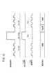
この特徴的な動作とは、[本実施形態の構成]の項目でも説明したように、図11に示すような、被写体14に対する動画撮影(被写体14に対して放射線16を繰り返し照射する放射線撮影)において、フレーム毎に、第2の放射線変換パネル28bを用いて動画像を取得して、取得した動画像を表示装置22に表示し、一方で、該第2の放射線変換パネル28bに対してリセット処理を行う時間帯では、第1の放射線変換パネル28aを用いて静止画像又は動画像を取得し、取得した静止画像又は動画像を表示装置22に表示するというものである。  As described in the item [Configuration of the present embodiment], this characteristic operation is a moving image shooting of the subject 14 (radiation shooting in which the subject 14 is repeatedly irradiated with the radiation 16) as illustrated in FIG. , For each frame, a moving image is acquired using the secondradiation conversion panel 28b, and the acquired moving image is displayed on thedisplay device 22, while being reset with respect to the secondradiation conversion panel 28b. In the time zone when processing is performed, a still image or a moving image is acquired using the firstradiation conversion panel 28a, and the acquired still image or moving image is displayed on thedisplay device 22.

すなわち、図11のタイムチャートにおいて、1番目から3番目までの放射線16の照射(パルス照射)では、低線量の放射線16を被写体14に照射して動画撮影を行う。この場合、放射線撮影装置10では、フレーム毎に、被写体14を透過した低線量の放射線16を動画用の第2の放射線変換パネル28bで動画像に変換する。取得された動画像は、フレーム毎に、放射線撮影装置10からコンソール20を介して表示装置22に送信され表示される。このように、第2の放射線変換パネル28bを用いて動画撮影が行われているため、第1の放射線変換パネル28aでは、リセット処理の実行が可能となる。  That is, in the time chart of FIG. 11, in the first to third irradiations (pulse irradiation) of theradiation 16, the subject 14 is irradiated with a low dose ofradiation 16 to perform moving image shooting. In this case, theradiation imaging apparatus 10 converts the low-dose radiation 16 transmitted through the subject 14 into a moving image for each frame by the secondradiation conversion panel 28b for moving images. The acquired moving image is transmitted and displayed from theradiation imaging apparatus 10 to thedisplay device 22 via theconsole 20 for each frame. As described above, since moving image shooting is performed using the secondradiation conversion panel 28b, the firstradiation conversion panel 28a can execute the reset process.

そして、撮影回数を重ねることにより第2の放射線変換パネル28bに対するリセット処理が必要となった場合には、高線量且つ比較的長い照射時間の放射線16を被写体14に照射して静止画撮影を行う(4番目のパルス照射)。この場合、放射線撮影装置10では、被写体14を透過した高線量の放射線16を静止画用の第1の放射線変換パネル28aで静止画像に変換する。取得された静止画像は、放射線撮影装置10からコンソール20を介して表示装置22に送信され、動画像に代えて表示される。このように、第1の放射線変換パネル28aを用いて静止画撮影が行われることにより、第2の放射線変換パネル28bでは、リセット処理の実行が可能となる。  When the secondradiation conversion panel 28b needs to be reset due to repeated imaging, the subject 14 is irradiated withradiation 16 having a high dose and a relatively long irradiation time, and still image shooting is performed. (4th pulse irradiation). In this case, theradiation imaging apparatus 10 converts the high-dose radiation 16 transmitted through the subject 14 into a still image by the firstradiation conversion panel 28a for still images. The acquired still image is transmitted from theradiation imaging apparatus 10 to thedisplay device 22 via theconsole 20, and is displayed instead of the moving image. As described above, by performing still image shooting using the firstradiation conversion panel 28a, the secondradiation conversion panel 28b can execute the reset process.

その後、低線量の放射線16を被写体14に照射して動画撮影を再開する(5番目以降のパルス照射)。この場合も、放射線撮影装置10では、フレーム毎に、被写体14を透過した低線量の放射線16を動画用の第2の放射線変換パネル28bで動画像に変換する。従って、取得された動画像は、フレーム毎に、放射線撮影装置10からコンソール20を介して表示装置22に送信され表示される。その際、再開された最初の動画撮影で取得された動画像(5番目のパルス照射により得られた動画像)が表示装置22に表示される場合、表示装置22は、これまで表示された静止画像に代えて、新たに送信されてきた動画像を表示する。第2の放射線変換パネル28bを用いた動画撮影が再開されることにより、第1の放射線変換パネル28aでは、リセット処理の実行が可能となる。  Thereafter, the subject 14 is irradiated with a low dose ofradiation 16 to resume moving image shooting (fifth pulse irradiation). Also in this case, theradiation imaging apparatus 10 converts the low-dose radiation 16 transmitted through the subject 14 into a moving image for each frame by the secondradiation conversion panel 28b for moving images. Accordingly, the acquired moving image is transmitted and displayed from theradiation imaging apparatus 10 to thedisplay device 22 via theconsole 20 for each frame. At that time, when the moving image (moving image obtained by the fifth pulse irradiation) acquired by the first moving image shooting restarted is displayed on thedisplay device 22, thedisplay device 22 displays the still image displayed so far. Instead of the image, the newly transmitted moving image is displayed. When the moving image capturing using the secondradiation conversion panel 28b is resumed, the firstradiation conversion panel 28a can execute the reset process.

このようにすれば、表示装置22に動画像又は静止画像を表示する場合に、画像が表示されない時間が発生して、画像を見ながら作業を行っている作業者が当該作業を中断してしまうことを回避することができる。  In this way, when a moving image or a still image is displayed on thedisplay device 22, a time during which the image is not displayed occurs, and an operator who is working while viewing the image interrupts the operation. You can avoid that.

なお、第2の放射線変換パネル28bを用いて動画撮影を行う場合には、基本的には、該動画撮影の時間帯に、第2の放射線変換パネル28bに対するリセット処理は実行されない。但し、図11に示すように、必要に応じて、第1の放射線変換パネル28aを用いた静止画撮影の時間帯に行われるリセット処理よりも短時間の簡易リセット処理を、動画撮影における放射線16の非照射時に行ってもよい。このようにすれば、残像の発生が抑制された動画像を取得することができる。  Note that when moving image shooting is performed using the secondradiation conversion panel 28b, basically, the reset process for the secondradiation conversion panel 28b is not executed during the moving image shooting time period. However, as shown in FIG. 11, if necessary, a simple reset process, which is shorter than the reset process performed in the still image capturing time zone using the firstradiation conversion panel 28 a, is applied to theradiation 16 in moving image capturing. You may carry out at the time of non-irradiation. In this way, it is possible to acquire a moving image in which the occurrence of afterimages is suppressed.

また、本実施形態では、第2の放射線変換パネル28bに対してリセット処理が実行される時間帯において、第1の放射線変換パネル28aを用いて複数枚の静止画撮影を行ってもよいし、又は、動画撮影を行ってもよい。複数枚の静止画撮影の場合には、例えば、複数の画素62aをまとめたビニングにより静止画を取得してもよい。  In the present embodiment, a plurality of still images may be captured using the firstradiation conversion panel 28a in a time zone in which the reset process is performed on the secondradiation conversion panel 28b. Alternatively, video shooting may be performed. In the case of shooting a plurality of still images, for example, a still image may be acquired by binning that combines a plurality ofpixels 62a.

[本実施形態の効果]
以上説明したように、本実施形態に係る放射線撮影装置10によれば、2つの放射線変換パネル28a、28bを用いて放射線撮影を行う場合に、動画撮影用の第2の放射線変換パネル28bに対するリセット処理中にのみ、静止画又は動画撮影用の第1の放射線変換パネル28aは、静止画撮影又は動画撮影を行うようにしている。このように、本実施形態では、第2の放射線変換パネル28bが動画撮影を行えない時間帯に、第1の放射線変換パネル28aが静止画撮影又は動画撮影を行うバックアップ機能を備えているため、リセット処理によって放射線画像(動画像又は静止画像)が取得できない状態になることを回避することができる。
[Effect of this embodiment]
As described above, according to theradiation imaging apparatus 10 according to the present embodiment, when radiation imaging is performed using the tworadiation conversion panels 28a and 28b, the reset to the secondradiation conversion panel 28b for moving image imaging is performed. Only during processing, the firstradiation conversion panel 28a for still image or moving image shooting is configured to perform still image shooting or moving image shooting. As described above, in the present embodiment, since the firstradiation conversion panel 28a has a backup function for performing still image shooting or moving image shooting in a time zone in which the secondradiation conversion panel 28b cannot perform moving image shooting, It can be avoided that the radiographic image (moving image or still image) cannot be acquired by the reset process.

また、前述のように、第2の放射線変換パネル28bによる動画撮影が行えない時間帯に、第1の放射線変換パネル28aによる静止画撮影又は動画撮影が行われるので、放射線撮影装置10では、放射線撮影が行えない時間帯は発生しない。そのため、放射線16を出力する放射線出力装置18と放射線撮影装置10との同期が取れていないことに起因して、放射線出力装置18が不意に放射線16を出力した場合であっても、放射線撮影装置10では、このような突発的な事態に対処して、動画撮影又は静止画撮影を適切に行うことが可能となる。  Further, as described above, since still image shooting or moving image shooting by the firstradiation conversion panel 28a is performed in a time zone during which moving image shooting by the secondradiation conversion panel 28b cannot be performed, theradiation imaging apparatus 10 There are no times when shooting is not possible. Therefore, even if theradiation output device 18 unexpectedly outputs theradiation 16 due to the synchronization between theradiation output device 18 that outputs theradiation 16 and theradiation imaging device 10, the radiation imaging device. 10 can cope with such a sudden situation and appropriately perform moving image shooting or still image shooting.

さらに、表示装置22に動画像又は静止画像を表示する場合、該表示装置22は、通常、第2の放射線変換パネル28bで取得された動画像を表示するが、該第2の放射線変換パネル28bに対するリセット処理中は、第1の放射線変換パネル28aで取得した静止画像又は動画像を表示することになる。このようにすれば、第2の放射線変換パネル28bに対するリセット処理中に、表示装置22で画像表示ができなくなることを回避することができる。この結果、表示装置22に表示された画像を見ながら所定の作業を行っている作業者(例えば、画像を見ながら患者にカテーテルを挿入する手術を行っている医師)は、前記作業を中断することなく、該作業を完遂することができる。  Further, when a moving image or a still image is displayed on thedisplay device 22, thedisplay device 22 normally displays the moving image acquired by the secondradiation conversion panel 28b, but the secondradiation conversion panel 28b. During the reset process, a still image or a moving image acquired by the firstradiation conversion panel 28a is displayed. In this way, it is possible to prevent thedisplay device 22 from displaying an image during the reset process for the secondradiation conversion panel 28b. As a result, an operator who performs a predetermined operation while viewing the image displayed on the display device 22 (for example, a doctor performing an operation of inserting a catheter into a patient while viewing the image) interrupts the operation. The work can be completed without any problem.

また、リセット制御部45は、第2の放射線変換パネル28bが動画像を取得可能な時間帯に、第1の放射線変換パネル28aに対してリセット処理を実行させるので、第1の放射線変換パネル28aは、残像の発生が抑制された高画質の静止画像又は動画像を取得することができる。なお、第2の放射線変換パネル28bにおいても、第1の放射線変換パネル28aによる静止画撮影又は動画撮影中にリセット処理を実行可能であるため、第2の放射線変換パネル28bで取得される動画像についても、残像の発生が抑制された動画像を取得することが可能である。  In addition, thereset control unit 45 causes the firstradiation conversion panel 28a to perform a reset process in a time zone in which the secondradiation conversion panel 28b can acquire a moving image, and thus the firstradiation conversion panel 28a. Can acquire a high-quality still image or moving image in which the occurrence of afterimages is suppressed. In the secondradiation conversion panel 28b, the reset process can be executed during still image shooting or moving image shooting by the firstradiation conversion panel 28a. Therefore, the moving image acquired by the secondradiation conversion panel 28b is used. Also, it is possible to obtain a moving image in which the occurrence of afterimages is suppressed.

また、リセット制御部45は、第2の放射線変換パネル28bが動画像を取得可能な時間帯において、放射線16の非照射時に、第1の放射線変換パネル28aを用いた静止画撮影又は動画撮影中に実行されるリセット処理よりも短時間の簡易リセット処理を、該第2の放射線変換パネル28bに対して実行させることも可能である。このような簡易リセット処理を実行すれば、第2の放射線変換パネル28bで取得される動画像に残像が重畳することを効果的に抑制することが可能となる。なお、所定のフレームレートで放射線16の照射が繰り返し行われる場合には、次回の放射線16の照射のタイミングを予測することが可能であるため、次のフレームでの動画像の欠落を発生させることなく、簡易リセット処理を実行することができる。  In addition, thereset control unit 45 is performing still image shooting or moving image shooting using the firstradiation conversion panel 28a when theradiation 16 is not irradiated in a time zone in which the secondradiation conversion panel 28b can acquire a moving image. It is also possible to cause the secondradiation conversion panel 28b to execute a simple reset process that is shorter than the reset process that is executed at the same time. If such a simple reset process is executed, it is possible to effectively suppress the afterimage from being superimposed on the moving image acquired by the secondradiation conversion panel 28b. Note that whenradiation 16 is repeatedly applied at a predetermined frame rate, it is possible to predict the timing of thenext radiation 16 irradiation, so that a moving image is missing in the next frame. And simple reset processing can be executed.

さらに、画素密度の低い第2の放射線変換パネル28bが動画用のパネルであり、画素密度の高い第1の放射線変換パネル28aが静止画又は動画用のパネルであれば、上記の各効果を容易に得ることができる。  Furthermore, if the secondradiation conversion panel 28b having a low pixel density is a moving image panel and the firstradiation conversion panel 28a having a high pixel density is a still image or moving image panel, the above effects can be easily achieved. Can get to.

このような画素密度の異なる2つの放射線変換パネル28a、28bにおいて、第2の放射線変換パネル28bのシンチレータで放射線16から変換された蛍光98が透過光102として第1の放射線変換パネル28aに入射した場合、該第1の放射線変換パネル28aの半導体層74aは、入射した透過光102を電荷94b、96bに変換することができる。すなわち、第1の放射線変換パネル28aでは、該第1の放射線変換パネル28aに照射された放射線16を電荷94a、96aに変換すると共に、入射した透過光102も電荷94b、96bに変換することができる。これにより、第1の放射線変換パネル28aの感度を高めると共に、該第1の放射線変換パネル28aにおいて、より高画質の静止画像又は動画像を取得することが可能となる。  In the tworadiation conversion panels 28a and 28b having different pixel densities, thefluorescence 98 converted from theradiation 16 by the scintillator of the secondradiation conversion panel 28b is incident on the firstradiation conversion panel 28a as the transmittedlight 102. In this case, thesemiconductor layer 74a of the firstradiation conversion panel 28a can convert the incident transmitted light 102 intocharges 94b and 96b. That is, in the firstradiation conversion panel 28a, theradiation 16 applied to the firstradiation conversion panel 28a is converted intocharges 94a and 96a, and the incident transmitted light 102 is also converted intocharges 94b and 96b. it can. As a result, the sensitivity of the firstradiation conversion panel 28a is increased, and a higher quality still image or moving image can be acquired by the firstradiation conversion panel 28a.

また、第2の放射線変換パネル28bが間接変換型の放射線変換パネルであるため、電気リセット処理に加え、バイアスリセット処理や光リセット処理も行うことが可能となる。従って、第2の放射線変換パネル28bの構成や状態に応じて好適なリセット処理を行うことができる。  In addition, since the secondradiation conversion panel 28b is an indirect conversion radiation conversion panel, it is possible to perform bias reset processing and light reset processing in addition to electrical reset processing. Therefore, a suitable reset process can be performed according to the configuration and state of the secondradiation conversion panel 28b.

また、フォトダイオード86bがMIS構造であれば、バイアスリセット処理を実行することが可能となる。この場合には、バイアスリセット処理の終了後、次のフレームの動画を取得するために、バイアスの極性を元に戻すか、又は、バイアスの供給を再開する処理が必要となるため、フォトダイオード86bが安定した状態に復帰するまで多少の時間はかかるが、残像を確実に消去することができる。  Further, if thephotodiode 86b has an MIS structure, it is possible to execute a bias reset process. In this case, after the bias reset process ends, in order to acquire the moving image of the next frame, it is necessary to restore the bias polarity or to restart the supply of the bias. Although it takes some time to return to a stable state, the afterimage can be reliably erased.

このように、本実施形態では、第1の放射線変換パネル28a及び第2の放射線変換パネル28bは、電気リセット処理、バイアスリセット処理及び光リセット処理のうち、少なくとも1つのリセット処理を行えば、残像の発生を効率よく抑制することができる。なお、本実施形態では、放射線撮影装置10の構成や状態等に応じて、1種類のリセット処理のみ実行したり、又は、複数の種類のリセット処理を使い分けて実行してもよいことは勿論である。  As described above, in the present embodiment, the firstradiation conversion panel 28a and the secondradiation conversion panel 28b perform the afterimage if at least one reset process among the electrical reset process, the bias reset process, and the light reset process is performed. Can be efficiently suppressed. In the present embodiment, it is needless to say that only one type of reset processing may be executed or a plurality of types of reset processing may be executed separately depending on the configuration or state of theradiation imaging apparatus 10. is there.

なお、本発明は、上述の実施の形態に限らず、本発明の要旨を逸脱することなく、種々の構成を採り得ることは勿論である。  Note that the present invention is not limited to the above-described embodiment, and it is needless to say that various configurations can be adopted without departing from the gist of the present invention.

10…放射線撮影装置
12…放射線撮影システム
14…被写体
16…放射線
18…放射線出力装置
20…コンソール
22…表示装置
28…放射線検出器
28a…第1の放射線変換パネル
28b…第2の放射線変換パネル
28c…リセット光源
30…駆動回路部
32…読出回路部
34…カセッテ制御部
40…バイアス電源
44…アドレス信号発生部
45…リセット制御部
47、58…画像処理部
62、62a、62b…画素
70a…第1の電荷検出部
70b…第2の電荷検出部
72a…第1の放射線検出部
72b…第2の放射線検出部
82a、82b…TFT
86b…フォトダイオード
94a、94b…正電荷
96a、96b…負電荷
98…蛍光
102…透過光
104…反射光
110a、110b…チャージアンプ
112a、112b…A/D変換器
116a、116b…オペアンプ
118a、118b…コンデンサ
120a、120b…スイッチ
122c…リセット光
DESCRIPTION OFSYMBOLS 10 ...Radiography apparatus 12 ...Radiography system 14 ...Subject 16 ...Radiation 18 ...Radiation output device 20 ...Console 22 ...Display device 28 ...Radiation detector 28a ... Firstradiation conversion panel 28b ... Secondradiation conversion panel 28c ... resetlight source 30 ... drivecircuit section 32 ...readout circuit section 34 ...cassette control section 40 ... biaspower supply 44 ... addresssignal generation section 45 ... resetcontrol sections 47 and 58 ...image processing sections 62, 62a and 62b ...pixel 70a ... 1 electriccharge detection part 70b ... 2nd electriccharge detection part 72a ... 1stradiation detection part 72b ... 2ndradiation detection part 82a, 82b ... TFT
86b ...Photodiodes 94a, 94b ...Positive charges 96a, 96b ...Negative charges 98 ...Fluorescence 102 ... Transmitted light 104 ... Reflected light 110a, 110b ...Charge amplifiers 112a, 112b ... A /D converters 116a, 116b ...Operational amplifiers 118a, 118b ...Capacitors 120a, 120b ...Switch 122c ... Reset light

Claims (9)

Translated fromJapanese
放射線の入射方向に沿って積層され、該放射線を放射線画像に変換可能な2つの放射線変換パネルと、
前記2つの放射線変換パネルに対して残像の発生を抑制するためのリセット処理を実行可能なリセット処理部と、
を有し、
一方の放射線変換パネルは、静止画像又は動画像を取得可能な放射線変換パネルであると共に、他方の放射線変換パネルは、動画像を取得可能な放射線変換パネルであり、
前記他方の放射線変換パネルに対して前記リセット処理部が前記リセット処理を実行可能な時間帯にのみ、前記一方の放射線変換パネルは、前記放射線を前記静止画像又は前記動画像に変換することを特徴とする放射線撮影装置。
Two radiation conversion panels stacked along the direction of incidence of radiation and capable of converting the radiation into a radiation image;
A reset processing unit capable of executing a reset process for suppressing the occurrence of an afterimage for the two radiation conversion panels;
Have
One radiation conversion panel is a radiation conversion panel capable of acquiring a still image or a moving image, and the other radiation conversion panel is a radiation conversion panel capable of acquiring a moving image,
The one radiation conversion panel converts the radiation into the still image or the moving image only in a time zone in which the reset processing unit can execute the reset process on the other radiation conversion panel. Radiation imaging device.
請求項1記載の装置において、
前記リセット処理部を制御するリセット制御部をさらに有し、
前記リセット制御部は、前記他方の放射線変換パネルが前記動画像を取得可能な時間帯に、前記一方の放射線変換パネルに対するリセット処理を実行するように前記リセット処理部を制御することを特徴とする放射線撮影装置。
The apparatus of claim 1.
A reset control unit for controlling the reset processing unit;
The reset control unit controls the reset processing unit to execute a reset process for the one radiation conversion panel in a time zone in which the other radiation conversion panel can acquire the moving image. Radiography equipment.
請求項2記載の装置において、
前記リセット制御部は、前記他方の放射線変換パネルが前記動画像を取得可能な時間帯において、前記放射線の非照射時に、前記他方の放射線変換パネルに対する前記リセット処理よりも短時間の簡易リセット処理を、該他方の放射線変換パネルに対して実行するように前記リセット処理部を制御することを特徴とする放射線撮影装置。
The apparatus of claim 2.
The reset control unit performs a simple reset process in a shorter time than the reset process for the other radiation conversion panel when the radiation is not irradiated in a time zone in which the other radiation conversion panel can acquire the moving image. The radiation imaging apparatus controls the reset processing unit so as to be executed on the other radiation conversion panel.
請求項1〜3のいずれか1項に記載の装置において、
前記2つの放射線変換パネルは、前記放射線を電荷に変換して蓄積する行列状に配置された複数の画素をそれぞれ有すると共に、画素密度が互いに異なる放射線変換パネルであることを特徴とする放射線撮影装置。
The device according to any one of claims 1 to 3,
The two radiation conversion panels are radiation conversion panels each having a plurality of pixels arranged in a matrix for converting and storing the radiation into electric charges and having different pixel densities. .
請求項4記載の装置において、
前記放射線の入射方向に沿って、前記一方の放射線変換パネルである第1の放射線変換パネルと、前記他方の放射線変換パネルである第2の放射線変換パネルとが順に積層され、
前記第1の放射線変換パネルは、前記放射線を電荷に直接変換する放射線検出部と、該放射線検出部から電荷を取り出す電荷取出部とを有する直接変換型の放射線変換パネルであり、
前記第2の放射線変換パネルは、前記第1の放射線変換パネルを透過した放射線を蛍光に変換するシンチレータと、前記蛍光を電荷に変換する光検出部とを有する間接変換型の放射線変換パネルであることを特徴とする放射線撮影装置。
The apparatus of claim 4.
Along the incident direction of the radiation, a first radiation conversion panel that is the one radiation conversion panel and a second radiation conversion panel that is the other radiation conversion panel are sequentially laminated,
The first radiation conversion panel is a direct conversion type radiation conversion panel having a radiation detection unit that directly converts the radiation into electric charge, and a charge extraction unit that extracts electric charge from the radiation detection unit,
The second radiation conversion panel is an indirect conversion type radiation conversion panel having a scintillator that converts the radiation transmitted through the first radiation conversion panel into fluorescence and a light detection unit that converts the fluorescence into electric charge. A radiographic apparatus characterized by that.
請求項5記載の装置において、
前記シンチレータで放射線から変換された蛍光が前記第1の放射線変換パネルに入射した場合に、該第1の放射線変換パネルは、入射した前記蛍光を電荷に変換可能に構成されていることを特徴とする放射線撮影装置。
The apparatus of claim 5.
When the fluorescence converted from radiation by the scintillator is incident on the first radiation conversion panel, the first radiation conversion panel is configured to be able to convert the incident fluorescence into an electric charge. Radiography equipment.
請求項5又は6記載の装置において、
前記光検出部は、前記蛍光を検出して電荷に変換する光検出素子を含み構成され、
前記リセット処理部は、リセット光源又はバイアス電源であり、
前記リセット光源から前記光検出素子にリセット光を照射することにより、又は、前記バイアス電源から前記光検出素子へのバイアスの供給を制御することにより、前記光検出素子に対するリセット処理が実行されることを特徴とする放射線撮影装置。
The device according to claim 5 or 6,
The photodetecting unit is configured to include a photodetecting element that detects the fluorescence and converts it into charges,
The reset processing unit is a reset light source or a bias power source,
The reset process for the photodetecting element is executed by irradiating the photodetecting element with reset light from the reset light source or by controlling the supply of a bias from the bias power source to the photodetecting element. A radiographic apparatus characterized by.
請求項7記載の装置において、
前記光検出素子がMIS構造のフォトダイオードである場合、前記バイアス電源は、前記フォトダイオードに供給するバイアスの極性を反転するか、又は、前記フォトダイオードへのバイアスの供給を停止することにより、前記フォトダイオードに対するリセット処理を実行することを特徴とする放射線撮影装置。
The apparatus of claim 7.
When the photodetection element is a photodiode having a MIS structure, the bias power source reverses the polarity of the bias supplied to the photodiode or stops supplying the bias to the photodiode, thereby A radiation imaging apparatus that performs a reset process on a photodiode.
請求項4〜8のいずれか1項に記載の装置において、
前記リセット処理部は、前記電荷の蓄積が可能な蓄積状態、又は、蓄積された前記電荷を読み出し可能な読出状態に前記各画素を切り換える駆動回路部と、読出状態の画素から電荷を読み出す読出回路部とであり、
前記駆動回路部により前記各画素を前記読出状態に切り換え、前記読出回路部により前記各画素に蓄積された電荷を読み出してグランドに放出させることで、前記各画素に対するリセット処理が実行されることを特徴とする放射線撮影装置。
The device according to any one of claims 4 to 8,
The reset processing unit includes a drive circuit unit that switches the pixels to an accumulation state in which the charge can be accumulated or a read state in which the accumulated charge can be read, and a readout circuit that reads out the charge from the pixel in the readout state And
The drive circuit unit switches each pixel to the readout state, and the readout circuit unit reads out the electric charge accumulated in each pixel and discharges it to the ground, whereby the reset process for each pixel is executed. A characteristic radiographic apparatus.
JP2011237109A2011-10-282011-10-28Radiographic imaging devicePendingJP2013096731A (en)

Priority Applications (1)

Application NumberPriority DateFiling DateTitle
JP2011237109AJP2013096731A (en)2011-10-282011-10-28Radiographic imaging device

Applications Claiming Priority (1)

Application NumberPriority DateFiling DateTitle
JP2011237109AJP2013096731A (en)2011-10-282011-10-28Radiographic imaging device

Publications (1)

Publication NumberPublication Date
JP2013096731Atrue JP2013096731A (en)2013-05-20

Family

ID=48618836

Family Applications (1)

Application NumberTitlePriority DateFiling Date
JP2011237109APendingJP2013096731A (en)2011-10-282011-10-28Radiographic imaging device

Country Status (1)

CountryLink
JP (1)JP2013096731A (en)

Cited By (4)

* Cited by examiner, † Cited by third party
Publication numberPriority datePublication dateAssigneeTitle
JP2015065433A (en)*2013-08-302015-04-09株式会社半導体エネルギー研究所Imaging apparatus
JP2015094736A (en)*2013-11-142015-05-18コニカミノルタ株式会社Bright burn effect elimination method and radiation image imaging apparatus with bright burn effect elimination feature
JP2017121063A (en)*2017-01-122017-07-06株式会社ニコン Imaging device
JP2018192056A (en)*2017-05-182018-12-06富士フイルム株式会社 Radiation image capturing apparatus, image processing apparatus, image processing method, and image processing program

Similar Documents

PublicationPublication DateTitle
US8532262B2 (en)Radiographic image capturing system
JP5666716B2 (en) Radiation moving image processing apparatus, radiation moving image capturing apparatus, radiation moving image capturing system, radiation moving image processing method, radiation moving image processing program, and storage medium
US8550709B2 (en)Imaging area specifying apparatus, radiographic system, imaging area specifying method, radiographic apparatus, and imaging table
US20130223592A1 (en)Radiographic system, drive control method for radiographic system, recording medium for drive control program and radiological image detection device
US9671506B2 (en)Radiographic image detection device, radiographic image detection method, and computer-readable storage medium
CN104160695B (en)Radiography device, radiography system, and radiography device control method
US9753159B2 (en)Radiographic imaging control device, radiographic imaging system, radiographic imaging device control method, and recording medium
CN103096799A (en)Radiographic imaging device and radiographic imaging system
WO2012165155A1 (en)Radiographic imaging device
US20130083897A1 (en)Radiographic image detecting device, radiographic image detecting method, and computer-readable storage medium
WO2013015267A1 (en)Radiographic equipment
JPWO2013027815A1 (en) Radiographic imaging system and radiographic imaging method
JP2013096731A (en)Radiographic imaging device
JP2013096759A (en)Radiation detection apparatus and radiation image photographing system
JP2011212427A (en)Radiation imaging system
JP5648404B2 (en) Radiographic imaging system and radiographic imaging device
WO2013136597A1 (en)Radiography control device, radiography system, radiography device control method, and radiography control program
JP2013096730A (en)Radiographic imaging device
JP2013096712A (en)Radiographic imaging device
WO2013015062A1 (en)Radiographic equipment
WO2013125325A1 (en)Radiography device, radiography system, radiography device control method, and radiography device control program
JP5608533B2 (en) Radiation imaging equipment
WO2013046916A1 (en)Radiographic imaging unit
WO2013125111A1 (en)Radiographic imaging control device, radiographic imaging system, control method for radiographic imaging device, and control program for radiographic imaging
WO2013062052A1 (en)Radiographic display system, radiographic display device, radiographic imaging device, program, radiograph display method, and recording medium

[8]ページ先頭

©2009-2025 Movatter.jp