JP2013093390A - Solar cell, manufacturing method therefor, and solar cell module - Google Patents
Solar cell, manufacturing method therefor, and solar cell moduleDownload PDFInfo
- Publication number
- JP2013093390A JP2013093390AJP2011233445AJP2011233445AJP2013093390AJP 2013093390 AJP2013093390 AJP 2013093390AJP 2011233445 AJP2011233445 AJP 2011233445AJP 2011233445 AJP2011233445 AJP 2011233445AJP 2013093390 AJP2013093390 AJP 2013093390A
- Authority
- JP
- Japan
- Prior art keywords
- layer
- hole
- electrode layer
- power generation
- solar cell
- Prior art date
- Legal status (The legal status is an assumption and is not a legal conclusion. Google has not performed a legal analysis and makes no representation as to the accuracy of the status listed.)
- Granted
Links
Images


Classifications
- Y—GENERAL TAGGING OF NEW TECHNOLOGICAL DEVELOPMENTS; GENERAL TAGGING OF CROSS-SECTIONAL TECHNOLOGIES SPANNING OVER SEVERAL SECTIONS OF THE IPC; TECHNICAL SUBJECTS COVERED BY FORMER USPC CROSS-REFERENCE ART COLLECTIONS [XRACs] AND DIGESTS
- Y02—TECHNOLOGIES OR APPLICATIONS FOR MITIGATION OR ADAPTATION AGAINST CLIMATE CHANGE
- Y02E—REDUCTION OF GREENHOUSE GAS [GHG] EMISSIONS, RELATED TO ENERGY GENERATION, TRANSMISSION OR DISTRIBUTION
- Y02E10/00—Energy generation through renewable energy sources
- Y02E10/50—Photovoltaic [PV] energy
- Y02E10/541—CuInSe2 material PV cells
- Y—GENERAL TAGGING OF NEW TECHNOLOGICAL DEVELOPMENTS; GENERAL TAGGING OF CROSS-SECTIONAL TECHNOLOGIES SPANNING OVER SEVERAL SECTIONS OF THE IPC; TECHNICAL SUBJECTS COVERED BY FORMER USPC CROSS-REFERENCE ART COLLECTIONS [XRACs] AND DIGESTS
- Y02—TECHNOLOGIES OR APPLICATIONS FOR MITIGATION OR ADAPTATION AGAINST CLIMATE CHANGE
- Y02P—CLIMATE CHANGE MITIGATION TECHNOLOGIES IN THE PRODUCTION OR PROCESSING OF GOODS
- Y02P70/00—Climate change mitigation technologies in the production process for final industrial or consumer products
- Y02P70/50—Manufacturing or production processes characterised by the final manufactured product
Landscapes
- Photovoltaic Devices (AREA)
Abstract
Description
Translated fromJapanese本発明は、太陽電池及びその製造方法、並びに前記太陽電池を複数個直列接続した太陽電池モジュールに関する。 The present invention relates to a solar cell, a manufacturing method thereof, and a solar cell module in which a plurality of the solar cells are connected in series.
太陽電池を複数個直列接続したグリッド型太陽電池モジュールが知られている。図1は、グリッド型太陽電池モジュールを構成する従来の太陽電池を例示する部分断面図である。図1を参照するに、太陽電池100において、金属層110上に、絶縁層であるバリア層120、裏面電極層130、発電層140、及び表面電極層150が順次積層されている。 A grid type solar cell module in which a plurality of solar cells are connected in series is known. FIG. 1 is a partial cross-sectional view illustrating a conventional solar cell constituting a grid type solar cell module. Referring to FIG. 1, in a
バリア層120、裏面電極層130、発電層140、及び表面電極層150には、金属層110の表面を露出する貫通孔100xが形成されている。貫通孔100x内には、貫通孔100xの内壁面を構成するバリア層120、裏面電極層130、発電層140、及び表面電極層150の各端面を被覆する絶縁層160を介して、導電材170が充填されている。導電材170は、貫通孔100x内から表面電極層150の表面の一部に延在している。 In the
このように、太陽電池100では、表面電極層150と金属層110とを導電材170を介して電気的に接続することにより、金属層110と裏面電極層130とから光起電力を取り出している(例えば、特許文献1参照)。 As described above, in the
しかしながら、太陽電池100では、金属層110上に製膜された各層とは別に、表面電極層150と金属層110とを電気的に接続する導電材170を貫通孔100x内に形成する必要があり、製造工程が煩雑化する問題があった。 However, in the
本発明は、上記の点に鑑みてなされたものであり、製造工程を簡略化できる太陽電池及びその製造方法、並びに前記太陽電池を複数個直列接続した太陽電池モジュールを提供することを課題とする。 This invention is made | formed in view of said point, and makes it a subject to provide the solar cell module which connected the solar cell which can simplify a manufacturing process, its manufacturing method, and the said solar cell in series. .
本太陽電池は、金属層と、前記金属層上に順次積層されたバリア層、裏面電極層、及び発電層と、前記発電層の表面から前記金属層の表面まで貫通する貫通孔と、前記裏面電極層と絶縁された状態で、前記金属層の表面と接するように前記貫通孔内に形成され、更に前記発電層上に延在する表面電極層と、を有することを要件とする。 The solar cell includes a metal layer, a barrier layer, a back electrode layer, and a power generation layer sequentially stacked on the metal layer, a through-hole penetrating from the surface of the power generation layer to the surface of the metal layer, and the back surface And a surface electrode layer that is formed in the through hole so as to be in contact with the surface of the metal layer while being insulated from the electrode layer, and further extends on the power generation layer.
本太陽電池の製造方法の一の形態は、金属層上にバリア層、裏面電極層、及び発電層を順次積層する積層工程と、前記発電層の表面から前記金属層の表面まで貫通する貫通孔を形成する貫通孔形成工程と、前記裏面電極層と絶縁された状態で前記金属層の表面と接するように前記貫通孔内に表面電極層を形成し、更に前記表面電極層を前記発電層上に延在させる表面電極層形成工程と、を有することを要件とする。 One embodiment of the method for producing the solar cell includes a laminating step of sequentially laminating a barrier layer, a back electrode layer, and a power generation layer on a metal layer, and a through-hole penetrating from the surface of the power generation layer to the surface of the metal layer Forming a through-hole, forming a surface electrode layer in the through-hole so as to be in contact with the surface of the metal layer in a state of being insulated from the back electrode layer, and further forming the surface electrode layer on the power generation layer And a surface electrode layer forming step to be extended.
本太陽電池の製造方法の他の形態は、バリア層上に、裏面電極層、及び発電層を順次積層する積層工程と、前記バリア層の前記裏面電極層形成面と反対側の面に金属層を形成する金属層形成工程と、前記バリア層、前記裏面電極層、及び前記発電層を貫通して前記金属層の表面を露出する貫通孔を形成する貫通孔形成工程と、前記裏面電極層と絶縁された状態で前記金属層の表面と接するように前記貫通孔内に表面電極層を形成し、更に前記表面電極層を前記発電層上に延在させる表面電極層形成工程と、を有することを要件とする。 Another embodiment of the method for manufacturing the solar cell includes a lamination step of sequentially laminating a back electrode layer and a power generation layer on the barrier layer, and a metal layer on the surface of the barrier layer opposite to the back electrode layer forming surface. Forming a metal layer, a through hole forming step of forming a through hole that penetrates the barrier layer, the back electrode layer, and the power generation layer to expose a surface of the metal layer, and the back electrode layer A surface electrode layer forming step of forming a surface electrode layer in the through hole so as to be in contact with the surface of the metal layer in an insulated state, and further extending the surface electrode layer on the power generation layer. Is a requirement.
開示の技術によれば、製造工程を簡略化できる太陽電池及びその製造方法、並びに前記太陽電池を複数個直列接続した太陽電池モジュールを提供できる。 According to the disclosed technology, it is possible to provide a solar cell that can simplify the manufacturing process, a manufacturing method thereof, and a solar cell module in which a plurality of the solar cells are connected in series.
以下、図面を参照して発明を実施するための形態について説明する。なお、各図面において、同一構成部分には同一符号を付し、重複した説明を省略する必要がある。 Hereinafter, embodiments for carrying out the invention will be described with reference to the drawings. In addition, in each drawing, the same code | symbol is attached | subjected to the same component and it is necessary to abbreviate | omit duplicate description.
〈第1の実施の形態〉
[第1の実施の形態に係る太陽電池の構造]
まず、第1の実施の形態に係る太陽電池の構造について、CIS系薄膜太陽電池を例にとって説明する。図2は、第1の実施の形態に係るCIS系薄膜太陽電池を例示する平面図である。図3は、図2のA−A線に沿う部分断面図である。各図は、CIS系薄膜太陽電池の平面形状が略正方形である場合の例を示し、CIS系薄膜太陽電池を平面視した場合(受光面側から視た場合)の1辺の方向をX方向、平面内でX方向に垂直な方向をY方向、厚さ方向をZ方向としている。又、便宜上、各断面図において各構成要素の紙面上側の面を表面、下側の面を裏面と称する。なお、CIS系薄膜とは、銅(Cu)、インジウム(In)、及びセレン(Se)を含有する化合物からなる薄膜である。<First Embodiment>
[Structure of Solar Cell According to First Embodiment]
First, the structure of the solar cell according to the first embodiment will be described by taking a CIS thin film solar cell as an example. FIG. 2 is a plan view illustrating the CIS thin film solar cell according to the first embodiment. 3 is a partial cross-sectional view taken along line AA in FIG. Each figure shows an example in which the planar shape of the CIS thin film solar cell is substantially square, and the direction of one side when the CIS thin film solar cell is viewed in plan (viewed from the light receiving surface side) is the X direction. In the plane, the direction perpendicular to the X direction is the Y direction, and the thickness direction is the Z direction. Further, for convenience, in each cross-sectional view, the upper surface of each component is referred to as the front surface, and the lower surface is referred to as the back surface. The CIS thin film is a thin film made of a compound containing copper (Cu), indium (In), and selenium (Se).
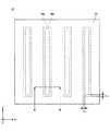
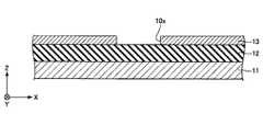
図2及び図3を参照するに、CIS系薄膜太陽電池10は、金属層11と、バリア層12と、裏面電極層13と、発電層14と、表面電極層15とを有し、金属層11上に、バリア層12、裏面電極層13、発電層14、及び表面電極層15が順次積層されている。CIS系薄膜太陽電池10の平面形状は、例えば10cm角〜15cm角程度の正方形とすることができる。以下、CIS系薄膜太陽電池10を構成する各要素について説明する。 2 and 3, the CIS-based thin film
金属層11は、裏面電極層13や発電層14等を形成する基体となる部分である。金属層11としては、例えば、ステンレスやアルミニウム合金等からなる金属板や、銅箔やアルミ箔等の金属箔等を用いることができる。金属層11の厚さは、例えば、数100μm程度とすることができる。なお、金属層11は薄いため、可撓性(フレキシブル性)を有する。 The
バリア層12は、金属層11上に形成されている。バリア層12は、金属層11と裏面電極層13とを絶縁するための絶縁層としての機能を有する。又、バリア層12は、金属層11に含有される金属イオン等が裏面電極層13側に移動することを防止する機能を有する。バリア層12の材料としては、例えば、シリカ(SiO2)、アルミナ(Al2O3)、ソーダライムガラス、シリコンナイトライド(Si3N4)等を用いることができる。バリア層12の厚さは、例えば、1〜3μm程度とすることができる。The
なお、バリア層12は原則として絶縁材料であればどのような材料を用いてもよいが、CIS系薄膜太陽電池10の場合には、ソーダライムガラスを用いることが好ましい。バリア層12としてソーダライムガラスを用いると、CIS系化合物からなる発電層14を製膜する際に、ソーダライムガラスに含有されるナトリウム(Na)が裏面電極層13を介して発電層14に拡散し、発電層14の結晶品質が向上するからである。 In principle, any material may be used for the
なお、バリア層12は単一の層から構成されてもよいし、複数の層が積層されて構成されてもよい。複数の層が積層されてバリア層12を構成する場合、単一の素材が複数積層された構成でもよいし、異なる素材が複数積層された構成であってもよい。例えば、金属層11上にアルミナを製膜し、アルミナ上にソーダライムガラスを積層してバリア層12を構成することができる。 In addition, the
裏面電極層13は、バリア層12上に形成されている。裏面電極層13は、CIS系薄膜太陽電池10の一方の電極となる層である。裏面電極層13の材料としては、例えば、モリブデン(Mo)、チタン(Ti)、クローム(Cr)等を用いることができる。裏面電極層13の厚さは、例えば、1〜3μm程度とすることができる。 The
貫通孔10xは、裏面電極層13を貫通してバリア層12の表面を露出する平面形状が細長状の貫通孔であり、Y軸に平行な方向に所定間隔で複数列並設されている。各貫通孔10xの幅(X方向)は、例えば、150μm程度とすることができる。なお、貫通孔10xは、本発明に係る他の貫通孔の代表的な一例である。 The through-
発電層14は、裏面電極層13上及び各貫通孔10x内に露出するバリア層12上に形成されている。発電層14は、各貫通孔10xの内壁面を構成する裏面電極層13の端面を覆うように形成されている。発電層14は、CIS系薄膜太陽電池10に照射された太陽光等を光電変換する部分であり、例えばp型半導体からなる。 The
発電層14としては、例えば、銅(Cu)、インジウム(In)、セレン(Se)からなる化合物や、銅(Cu)、インジウム(In)、ガリウム(Ga)、セレン(Se)、硫黄(S)からなる化合物等の、少なくとも銅(Cu)、インジウム(In)、及びセレン(Se)を含有する化合物を用いることができる。前記化合物の一例を挙げれば、CuInSe2、Cu(InGa)Se2、Cu(InGa)(SSe)2等である。発電層14の厚さは、例えば、1〜3μm程度とすることができる。As the
貫通孔10yは、発電層14の表面から金属層11の表面まで貫通して金属層11の表面を露出する平面形状が細長状の貫通孔であり、Y軸に平行な方向に所定間隔で複数列並設されている。各貫通孔10yは、平面視において、各貫通孔10xに囲まれるように形成されている。換言すれば、各貫通孔10yは、平面視において各貫通孔10xよりも内側に形成されている。 The through-
平面視において、各貫通孔10yの周囲には、バリア層12が環状に露出している。各貫通孔10yの幅(X方向)は、例えば、70μm程度とすることができる。各貫通孔10xの内壁面と各貫通孔10yの内壁面の平面視における距離L1(バリア層12の露出部分の幅)は全周において略一定であり、例えば、40μm程度とすることができる。本実施の形態では、貫通孔10x及び10yを4列ずつ並設しているが、並設する列数は任意に設定して構わない。なお、貫通孔10yは、本発明に係る貫通孔の代表的な一例である。In plan view, the
なお、発電層14の表面にバッファ層(図示せず)を形成してもよい。バッファ層は、発電層14からの電流の漏出を防止する機能を有する高抵抗の層である。バッファ層の材料としては、例えば、亜鉛化合物、硫化亜鉛(ZnS)、硫化カドミウム(CdS)、硫化インジウム(InS)等を用いることができる。バッファ層の厚さは、例えば、5〜50nm程度とすることができる。 A buffer layer (not shown) may be formed on the surface of the
表面電極層15は、n型半導体からなる透明な層であり、発電層14上(発電層14の表面、又は、バッファ層が形成されている場合にはバッファ層の表面、以降同様。)及び各貫通孔10y内に形成されている。各貫通孔10y内に形成された表面電極層15の下端面は金属層11の表面と接触している。つまり、表面電極層15と金属層11とは電気的に接続されている。表面電極層15と発電層14とは、pn接合を形成している。表面電極層15は、CIS系薄膜太陽電池10の他方の電極となる層である。 The
各貫通孔10y内に形成された表面電極層15は、裏面電極層13の端面と絶縁する必要がある。本実施の形態では、裏面電極層13と絶縁するために専用の絶縁層を設けることなく、発電層14を各貫通孔10xの内壁面を構成する裏面電極層13の端面を覆うように形成して裏面電極層13と各貫通孔10y内に形成された表面電極層15とを絶縁している。裏面電極層13と各貫通孔10y内に形成された表面電極層15とを絶縁できれば、前述の距離L1は任意の値に設定して構わない。The
このように、表面電極層15は、裏面電極層13と絶縁された状態で金属層11の表面と接するように各貫通孔10y内に形成され、更に発電層14上に延在している。つまり、各貫通孔10y内に形成された表面電極層15により、発電層14上に形成された表面電極層15と金属層11とを電気的に接続している。 Thus, the
表面電極層15としては、例えば、酸化亜鉛系薄膜(ZnO)やITO(Indium Tin Oxide)薄膜等の透明かつ低抵抗な膜を用いることができる。表面電極層15として酸化亜鉛系薄膜(ZnO)を用いる場合には、硼素(B)やガリウム(Ga)、アルミニウム(Al)等をドーパントとして添加することにより、低抵抗化でき好適である。発電層14上の表面電極層15の厚さは、例えば、2〜4μm程度とすることができる。 As the
このように、表面電極層15を表面電極層15よりも低抵抗の金属層11と電気的に接続することにより、表面電極層15と発電層14とで生じた光起電力を、低抵抗の金属層11及び裏面電極層13から取り出すことができる。 Thus, by electrically connecting the
[第1の実施の形態に係る太陽電池の製造方法]
次に、第1の実施の形態に係る太陽電池の製造方法についてCIS系薄膜太陽電池を例にとって説明する。図4〜図9は、第1の実施の形態に係るCIS系薄膜太陽電池の製造工程を例示する図である。なお、図4〜図9は、図2のA−A断面に対応する部分断面図である。[Method of Manufacturing Solar Cell According to First Embodiment]
Next, a method for manufacturing the solar cell according to the first embodiment will be described by taking a CIS-based thin film solar cell as an example. 4-9 is a figure which illustrates the manufacturing process of the CIS type thin film solar cell which concerns on 1st Embodiment. 4 to 9 are partial cross-sectional views corresponding to the AA cross section of FIG.
まず、図4に示す工程では、金属層11を準備し、準備した金属層11上にバリア層12を形成する。金属層11としては、例えば、ステンレスやアルミニウム合金等からなる金属板や、銅箔やアルミ箔等の金属箔等を用いることができる。金属層11の厚さは、例えば、数100μm程度とすることができる。 First, in the step shown in FIG. 4, the
バリア層12は、例えば、シリカ(SiO2)、アルミナ(Al2O3)、ソーダライムガラス、シリコンナイトライド(Si3N4)等の材料を用いて、スパッタ法等により、金属層11上に形成できる。バリア層12の厚さは、例えば、1〜3μm程度とすることができる。The
次に、図5に示す工程では、バリア層12上に裏面電極層13を形成する。裏面電極層13は、例えば、モリブデン(Mo)、チタン(Ti)、クローム(Cr)等の高耐蝕性で高融点の金属材料を用いて、スパッタ法等により、バリア層12上に形成できる。裏面電極層13の厚さは、例えば、1〜3μm程度とすることができる。 Next, in the step shown in FIG. 5, the
次に、図6に示す工程では、裏面電極層13を貫通してバリア層12の表面を露出する平面形状が細長状の貫通孔10xを、Y軸に平行な方向に所定間隔で複数列並設する。例えば、YAGレーザ等のレーザ光を裏面電極層13の一部に照射することにより、レーザ光が照射された部分の裏面電極層13が除去され、各貫通孔10xが形成される。各貫通孔10xの幅(X方向)は、例えば、150μm程度とすることができる。 Next, in the step shown in FIG. 6, through-
次に、図7に示す工程では、裏面電極層13上及び各貫通孔10x内に露出するバリア層12上に、発電層14を形成する。換言すれば、裏面電極層13を覆うと共に各貫通孔10x内を充填するようにバリア層12上に発電層14を積層する。発電層14としては、例えば、前述のような銅(Cu)、インジウム(In)、及びセレン(Se)を含有する化合物を用いることができる。発電層14は、例えば、図6に示す構造体を500℃程度以上に加熱し、裏面電極層13上及び各貫通孔10x内に露出するバリア層12に銅(Cu)、インジウム(In)、及びセレン(Se)を含有する原料を適当な組合せで同時に蒸着する多源同時蒸着法によって形成できる。発電層14は、セレン化/硫化法等により形成してもよい。 Next, in the process shown in FIG. 7, the
次に、図8に示す工程では、各貫通孔10xの内側に、発電層14の表面から金属層11の表面まで貫通して金属層11の表面を露出する平面形状が細長状の貫通孔10yを形成する。各貫通孔10yは、各貫通孔10xの内壁面を構成する裏面電極層13の端面が発電層14により覆われるように、平面視において各貫通孔10xよりも内側に形成する。例えば、YAGレーザ等のレーザ光を発電層14及びバリア層12の一部に照射することにより、レーザ光が照射された部分の発電層14及びバリア層12が除去され、各貫通孔10yが形成される。但し、レーザを用いずに、機械的に各貫通孔10yを形成してもよい(メカニカルスクライブ)。 Next, in the process shown in FIG. 8, the through
各貫通孔10yの幅(X方向)は、例えば、70μm程度とすることができる。各貫通孔10yは、各貫通孔10xの内壁面と各貫通孔10yの内壁面の平面視における距離L1が略一定となるように形成する。距離L1は、例えば、40μm程度とすることができる。The width (X direction) of each through-
次に、図9に示す工程では、発電層14上及び各貫通孔10y内に、表面電極層15を形成する。換言すれば、裏面電極層13と絶縁された状態で金属層11の表面と接するように各貫通孔10y内に表面電極層15を形成し、更に各貫通孔10y内の表面電極層15を発電層14上に延在させる。各貫通孔10xの内壁面を構成する裏面電極層13の端面は絶縁層として機能する発電層14により覆われているため、裏面電極層13と各貫通孔10y内に形成された表面電極層15とは絶縁される。 Next, in the process shown in FIG. 9, the
表面電極層15は、例えば、硼素(B)やガリウム(Ga)、アルミニウム(Al)等をドーパントとして添加した酸化亜鉛系薄膜(ZnO)や、ITO(Indium Tin Oxide)薄膜等の透明かつ低抵抗な膜を、MOCVD法やスパッタ法等により、発電層14上及び各貫通孔10y内に形成できる。発電層14上の表面電極層15の厚さは、例えば、2〜4μm程度とすることができる。 The
なお、図7に示す工程よりも前に、金属層11の裏面側にモリブデン(Mo)や硫黄(S)等のVI族元素に対して耐腐食性を有する耐腐食膜を形成してもよい。図7に示す工程で発電層14を形成する際に、セレン(Se)や硫黄(S)等のVI族元素が金属層11の裏面を腐食することを防止するためである。 Prior to the step shown in FIG. 7, a corrosion-resistant film having corrosion resistance against Group VI elements such as molybdenum (Mo) and sulfur (S) may be formed on the back surface side of the
又、図7に示す工程よりも後に、発電層14の表面にバッファ層を形成してもよい。バッファ層は、例えば、亜鉛化合物、硫化亜鉛(ZnS)、硫化カドミウム(CdS)、硫化インジウム(InS)等の材料を用いて、溶液成長法(CBD法)等により、発電層14の表面に形成できる。バッファ層の厚さは、例えば、5〜50nm程度とすることができる。なお、溶液成長法(CBD法)とは、前駆体となる化学種を含む溶液に基材を浸し、溶液と基材表面との間で不均一反応を進行させることによって薄膜を基材上に析出させる方法である。 Further, a buffer layer may be formed on the surface of the
[第1の実施の形態に係る太陽電池モジュールの構造]
次に、CIS系薄膜太陽電池を複数個直接に接続したCIS系薄膜太陽電池モジュールの構造について説明する。[Structure of Solar Cell Module According to First Embodiment]
Next, the structure of a CIS thin film solar cell module in which a plurality of CIS thin film solar cells are directly connected will be described.
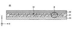
図10は、第1の実施の形態に係るCIS系薄膜太陽電池モジュールを例示する断面図である。図11は、図10のB部の部分断面図である。 FIG. 10 is a cross-sectional view illustrating the CIS thin film solar cell module according to the first embodiment. FIG. 11 is a partial cross-sectional view of a portion B in FIG.
図10を参照するに、CIS系薄膜太陽電池モジュール20は、複数のCIS系薄膜太陽電池10を直列に接続して封止材21で封止し、更に、封止材21の表面を覆う表面保護材22を形成し、封止材21の裏面を覆う裏面保護材23を形成したグリッド型構造を有する。 Referring to FIG. 10, a CIS thin film
封止材21の材料としては、例えば、EVA(エチレン・ビニル・アセテート)やPVB(ポリビニルブチラール)等を用いることができる。表面保護材22の材料としては、強化ガラスやアクリル系樹脂等を用いることができる。裏面保護材23の材料としては、ガラスやPET(ポリエチレンテレフタレート)等を用いることができる。 As a material of the sealing
図11を参照するに、各CIS系薄膜太陽電池10の端部(一端側のみ)の発電層14及び表面電極層15が除去されて、裏面電極層13の表面が露出している。そして、発電層14及び表面電極層15から露出した裏面電極層13の表面が、隣接して配置された他のCIS系薄膜太陽電池10の金属層11の裏面と接して電気的に接続されている。なお、裏面電極層13の表面と金属層11の裏面とは直接接しても構わないし、はんだや導電性ペースト等の導電性の接合部を介して接しても構わない。 Referring to FIG. 11, the
なお、図示はしていないが、金属層11の一端及び裏面電極層13の一端を、一対の外部端子として、封止材21、表面保護材22、及び裏面保護材23から露出する(配線を引き出す)必要がある。一対の外部端子から、各CIS系薄膜太陽電池10で生じた光起電力を取り出すことができる。 Although not shown, one end of the
このように、複数個のCIS系薄膜太陽電池10を直列に接続してCIS系薄膜太陽電池モジュール20とすることにより、所望の起電力を得ることができる。 Thus, a desired electromotive force can be obtained by connecting a plurality of CIS thin film
なお、図11に示した方法以外で、複数個のCIS系薄膜太陽電池10を直列に接続してもよい。例えば、CIS系薄膜太陽電池10の発電層14及び表面電極層15から露出した裏面電極層13の表面と、隣接して配置された他のCIS系薄膜太陽電池10の金属層11の裏面とをバスバー電極リボンによって接続してもよい。 In addition, you may connect the some CIS type thin film
このように、第1の実施の形態に係るCIS系薄膜太陽電池10では、各貫通孔10y内に形成された表面電極層15により、発電層14上に形成された表面電極層15と金属層11とを電気的に接続している。これにより、従来の太陽電池のように、金属層上に製膜された各層とは別に、表面電極層と金属層とを電気的に接続する専用の導電材を各貫通孔内に形成する必要がないため、CIS系薄膜太陽電池10の製造工程を簡略化できる。 Thus, in the CIS-based thin film
又、各貫通孔10xの内壁面を構成する裏面電極層13の端面を覆うように発電層14を形成して、裏面電極層13と各貫通孔10y内に形成された表面電極層15とを発電層14により絶縁している。これにより、従来の太陽電池のように、表面電極層と金属層とを電気的に接続する導電材と裏面電極層とを絶縁する専用の絶縁層を形成する必要がないため、CIS系薄膜太陽電池10の製造工程を簡略化できる。 Further, the
〈第1の実施の形態の変形例1〉
第1の実施の形態の変形例1では、貫通孔10x及び10yをそれぞれ貫通孔10s及び10tに置換する例を示す。なお、第1の実施の形態の変形例1において、既に説明した実施の形態と同一構成部品についての説明は省略する。<Variation 1 of the first embodiment>
The first modification of the first embodiment shows an example in which the through
図12は、第1の実施の形態の変形例1に係るCIS系薄膜太陽電池を例示する平面図である。第1の実施の形態では、貫通孔10x及び10yをそれぞれ平面形状が細長状(平面形状が細長い矩形状)の孔としたが(図2参照)、例えば、図12に示す貫通孔10s及び10tのように、それぞれの平面形状を円形としてもよい。或いは、各貫通孔の平面形状を楕円形や矩形、その他の任意の形状としてもよい。なお、図12のA−A線に沿う断面図は図3と同様であるため、図示は省略する。 FIG. 12 is a plan view illustrating a CIS-based thin film solar cell according to Modification 1 of the first embodiment. In the first embodiment, each of the through
貫通孔10sは、裏面電極層13を貫通し、バリア層12の表面を露出する平面形状が円形の孔であり、所定間隔で複数個縦横に配列されている。各貫通孔10sの直径は、例えば、150μm程度とすることができる。貫通孔10tは、発電層14の表面から金属層11の表面まで貫通して金属層11の表面を露出する平面形状が円形の孔であり、所定間隔で複数個縦横に配列されている。なお、貫通孔10sは、本発明に係る他の貫通孔の代表的な一例である。 The through holes 10 s are holes having a circular planar shape that penetrates the
各貫通孔10tは各貫通孔10sよりも小径であり、各貫通孔10tは、平面視において、各貫通孔10sに囲まれるように略同心円状に形成されている。平面視において、各貫通孔10tの周囲には、バリア層12が円環状に露出している。各貫通孔10tの直径は、例えば、70μm程度とすることができる。各貫通孔10sの内壁面と各貫通孔10tの内壁面の平面視における距離L1(バリア層12の露出部分の幅)は全周において略一定であり、例えば、40μm程度とすることができる。なお、貫通孔10tは、本発明に係る貫通孔の代表的な一例である。Each through hole 10t has a smaller diameter than each through
このように、バリア層12や発電層14、裏面電極層13等に形成する貫通孔の形状は任意に決定して構わない。 Thus, the shape of the through hole formed in the
〈第1の実施の形態の変形例2〉
第1の実施の形態の変形例2では、貫通孔10x及び10yをそれぞれ貫通孔10m及び10nに置換する例を示す。なお、第1の実施の形態の変形例2において、既に説明した実施の形態と同一構成部品についての説明は省略する。<Modification 2 of the first embodiment>
Modification 2 of the first embodiment shows an example in which the through
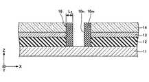
図13は、第1の実施の形態の変形例2に係るCIS系薄膜太陽電池を例示する部分断面図である。なお、図13は、図2のA−A断面に対応する断面図である。図13を参照するに、CIS系薄膜太陽電池10Aにおいて、貫通孔10mは、バリア層12、裏面電極層13、及び発電層14を貫通して金属層11の表面を露出する平面形状が細長状の貫通孔であり、Y軸に平行な方向に所定間隔で複数列並設されている。各貫通孔10mの幅(X方向)は、例えば、150μm程度とすることができる。 FIG. 13 is a partial cross-sectional view illustrating a CIS-based thin film solar cell according to Modification 2 of the first embodiment. 13 is a cross-sectional view corresponding to the AA cross section of FIG. Referring to FIG. 13, in the CIS-based thin film
各貫通孔10mの内壁面を構成するバリア層12、裏面電極層13、及び発電層14の各端面を覆うように、絶縁層16が形成されている。絶縁層16としては、例えば、ナイロン、ポリブチレンテレフタレート、ポリプロピレン等の熱可塑性ポリマ等を用いることができる。なお、貫通孔10mは、本発明に係る他の貫通孔の代表的な一例である。 An insulating
貫通孔10nは、発電層14の表面から金属層11の表面まで貫通して金属層11の表面を露出する平面形状が細長状の貫通孔であり、Y軸に平行な方向に所定間隔で複数列並設されている。絶縁層16は、各貫通孔nの内壁面を構成している。各貫通孔10nは、平面視において、各貫通孔10mに囲まれるように形成されている。換言すれば、各貫通孔10nは、平面視において各貫通孔10mよりも内側に形成されている。 The through-
各貫通孔10nの幅(X方向)は、例えば、70μm程度とすることができる。各貫通孔10mの内壁面と各貫通孔10nの内壁面の平面視における距離L2(絶縁層16の幅)は全周において略一定であり、例えば、40μm程度とすることができる。なお、貫通孔10nは、本発明に係る貫通孔の代表的な一例である。The width (X direction) of each through-
表面電極層15は、発電層14上及び各貫通孔10n内に形成されている。各貫通孔10n内に形成された表面電極層15の下端面は金属層11の表面と接触している。つまり、表面電極層15と金属層11とは電気的に接続されている。 The
各貫通孔10n内に形成された表面電極層15は、裏面電極層13の端面と絶縁する必要がある。本実施の形態では、バリア層12、裏面電極層13、及び発電層14を貫通する貫通孔10mを形成し、各貫通孔10mの内壁面を構成する少なくとも裏面電極層13の端面を絶縁層16で覆うことにより、裏面電極層13と各貫通孔10n内に形成された表面電極層15とを絶縁している。裏面電極層13と各貫通孔10n内に形成された表面電極層15とを絶縁できれば、前述の距離L2(絶縁層16の幅)は任意の値に設定して構わない。The
なお、第1の実施の形態の変形例1と同様に、各貫通孔10m及び10nの形状は任意に決定してよく、例えば、各貫通孔10m及び10nの平面形状を円形等とすることができる。 As in the first modification of the first embodiment, the shape of each through
[第1の実施の形態の変形例2に係る太陽電池の製造方法]
次に、第1の実施の形態の変形例2に係る太陽電池の製造方法について、CIS系薄膜太陽電池を例にとって説明する。図14〜図18は、第1の実施の形態の変形例2に係るCIS系薄膜太陽電池の製造工程を例示する図である。なお、図14〜図18は、図2のA−A断面に対応する断面図である。[Method for Manufacturing Solar Cell According to Modification 2 of First Embodiment]
Next, a method for manufacturing a solar cell according to Modification Example 2 of the first embodiment will be described using a CIS-based thin film solar cell as an example. 14 to 18 are diagrams illustrating a manufacturing process of the CIS-based thin film solar cell according to the second modification of the first embodiment. 14 to 18 are cross-sectional views corresponding to the AA cross section of FIG.
まず、図14に示す工程では、第1の実施の形態の図4及び図5の工程を実行後、裏面電極層13上に、発電層14を形成する。発電層14の材料や形成方法等は前述の通りである。 First, in the process shown in FIG. 14, the
次に、図15に示す工程では、バリア層12、裏面電極層13、及び発電層14を貫通して金属層11の表面を露出する平面形状が細長状の貫通孔10mをY軸に平行な方向に所定間隔で複数列並設する。例えば、YAGレーザ等のレーザ光をバリア層12、裏面電極層13、及び発電層14の一部に照射することにより、レーザ光が照射された部分のバリア層12、裏面電極層13、及び発電層14が除去され、各貫通孔10mが形成される。但し、レーザを用いずに、機械的に各貫通孔10mを形成してもよい。各貫通孔10mの幅(X方向)は、例えば、150μm程度とすることができる。 Next, in the process shown in FIG. 15, the planar shape that exposes the surface of the
次に、図16に示す工程では、例えば印刷法等を用いて、各貫通孔10m内に未硬化の熱可塑性ポリマ等(例えば、ナイロン、ポリブチレンテレフタレート、ポリプロピレン等)を充填し、その後硬化温度以上に加熱して硬化させ、絶縁層16を形成する。少なくとも各貫通孔10mの内壁面を構成する裏面電極層13の端面は、絶縁層16で覆われる。絶縁層16の表面は、発電層14の表面と略面一とすることができる。 Next, in the step shown in FIG. 16, for example, a printing method or the like is used to fill each through
次に、図17に示す工程では、各貫通孔10mの内側に、絶縁層16を発電層14の表面から金属層11の表面まで貫通して金属層11の表面を露出する平面形状が細長状の貫通孔10nを形成する。各貫通孔10nは、絶縁層16が内壁面を構成するように、平面視において各貫通孔10mよりも内側に形成する。例えば、YAGレーザ等のレーザ光を絶縁層16の一部に照射することにより、レーザ光が照射された部分の絶縁層16が除去され、各貫通孔10nが形成される。但し、レーザを用いずに、機械的に各貫通孔10nを形成してもよい。 Next, in the step shown in FIG. 17, the planar shape that exposes the surface of the
各貫通孔10nの幅(X方向)は、例えば、70μm程度とすることができる。各貫通孔10nは、各貫通孔10mの内壁面と各貫通孔10nの内壁面の平面視における距離L2が略一定となるように形成する。距離L2は、例えば、40μm程度とすることができる。The width (X direction) of each through-
次に、図18に示す工程では、発電層14上及び各貫通孔10n内に、表面電極層15を形成する。換言すれば、裏面電極層13と絶縁された状態で金属層11の表面と接するように各貫通孔10n内に表面電極層15を形成し、更に各貫通孔10n内の表面電極層15を発電層14上に延在させる。各貫通孔10mの内壁面を構成する裏面電極層13の端面は絶縁層16により覆われているため、裏面電極層13と各貫通孔10n内に形成された表面電極層15とは絶縁される。表面電極層15の材料や形成方法等は前述の通りである。以上の工程により、図13に示すCIS系薄膜太陽電池10Aが完成する。 Next, in the step shown in FIG. 18, the
図19は、第1の実施の形態の変形例3に係るCIS系薄膜太陽電池を例示する部分断面図である。図13に示すCIS系薄膜太陽電池10Aを、図19に示すに示すCIS系薄膜太陽電池10Bのように変形してもよい。つまり、絶縁層16は、裏面電極層13と各貫通孔10n内に形成された表面電極層15とを絶縁するために設けているので、絶縁層16は、少なくとも裏面電極層13の端面を覆うように形成すればよい。CIS系薄膜太陽電池10Bを製造するには、図16に示す工程で、裏面電極層13の端面を覆う程度に各貫通孔10m内に未硬化の熱可塑性ポリマ等を形成すればよい。その他の製造工程は、CIS系薄膜太陽電池10Aと同様である。 FIG. 19 is a partial cross-sectional view illustrating a CIS-based thin film solar cell according to Modification 3 of the first embodiment. The CIS thin film
このように、第1の実施の形態の変形例2に係るCIS系薄膜太陽電池10A、又は、第1の実施の形態の変形例3に係るCIS系薄膜太陽電池10Bでは、各貫通孔10n内に形成された表面電極層15により、発電層14上に形成された表面電極層15と金属層11とを電気的に接続している。これにより、従来の太陽電池のように、金属層上に製膜された各層とは別に、表面電極層と金属層とを電気的に接続する専用の導電材を各貫通孔内に形成する必要がないため、CIS系薄膜太陽電池10A及び10Bの製造工程を簡略化できる。 As described above, in the CIS-based thin film
以上、好ましい実施の形態及びその変形例について詳説したが、上述した実施の形態及びその変形例に制限されることはなく、特許請求の範囲に記載された範囲を逸脱することなく、上述した実施の形態及びその変形例に種々の変形及び置換を加えることができる。 The preferred embodiment and its modification have been described in detail above, but the present invention is not limited to the above-described embodiment and its modification, and the above-described implementation is performed without departing from the scope described in the claims. Various modifications and substitutions can be added to the embodiment and its modifications.
例えば、上述した実施の形態及びその変形例では、CIS系薄膜太陽電池を例にとって太陽電池の説明をしたが、本発明はCIS系薄膜太陽電池以外にも適用可能である。本発明を適用可能な太陽電池の一例を挙げれば、アモルファスシリコン系太陽電池、結晶シリコン系太陽電池、CIS系以外の化合物系太陽電池等である。CIS系以外の化合物系太陽電池とは、例えば、発電層が銅(Cu)、亜鉛(Zn)、錫(Sn)、及びカルコゲン元素(セレン(Se)又は硫黄(S))を含有する化合物からなるCZTS系太陽電池や、発電層がカドミウム(Cd)及びテルル(Te)を含有する化合物からなるCdTe系太陽電池等である。 For example, in the above-described embodiment and its modification, the solar cell has been described by taking the CIS thin film solar cell as an example, but the present invention can be applied to other than the CIS thin film solar cell. Examples of solar cells to which the present invention can be applied include amorphous silicon solar cells, crystalline silicon solar cells, and compound solar cells other than CIS. A compound solar cell other than CIS is, for example, a compound in which the power generation layer contains copper (Cu), zinc (Zn), tin (Sn), and a chalcogen element (selenium (Se) or sulfur (S)). CZTS solar cells, and CdTe solar cells whose power generation layer is made of a compound containing cadmium (Cd) and tellurium (Te).
又、上述した実施の形態及びその変形例では、金属層11上に、バリア層12、裏面電極層13、発電層14、及び表面電極層15を順次積層した。しかし、例えば、バリア層12としてポリイミドフィルム等を用い、バリア層12を構成するポリイミドフィルムを基体として、その上に裏面電極層13、発電層14、及び表面電極層15を順次積層する工程としてもよい。この場合には、バリア層12の裏面側に金属層11を形成することができる。金属層11としては、例えば、銅(Cu)やアルミニウム(Al)等をめっき法や蒸着法等によりバリア層12の裏面側に形成することができる。金属層11の厚さは、例えば、数10μm程度とすることができる。 In the above-described embodiment and its modifications, the
つまり、バリア層12上に、裏面電極層13、及び発電層14を順次積層する積層工程と、バリア層12の裏面電極層13の形成面と反対側の面に金属層11を形成する金属層形成工程と、発電層14の表面から金属層11の表面まで貫通する貫通孔10yを形成する貫通孔形成工程と、裏面電極層13と絶縁された状態で金属層11の表面と接するように貫通孔10y内に表面電極層15を形成し、更に表面電極層15を発電層14上に延在させる表面電極層形成工程と、を有する太陽電池の製造方法により、CIS系薄膜太陽電池10等を製造できる。 That is, a lamination process of sequentially laminating the
10、10A、10B CIS系薄膜太陽電池
10m、10n、10s、10t、10x、10y 貫通孔
11 金属層
12 バリア層
13 裏面電極層
14 発電層
15 表面電極層
16 絶縁層
20 CIS系薄膜太陽電池モジュール
21 封止材
22 表面保護材
23 裏面保護材
L1、L2 距離10, 10A, 10B CIS thin film
Claims (13)
Translated fromJapanese前記金属層上に順次積層されたバリア層、裏面電極層、及び発電層と、
前記発電層の表面から前記金属層の表面まで貫通する貫通孔と、
前記裏面電極層と絶縁された状態で、前記金属層の表面と接するように前記貫通孔内に形成され、更に前記発電層上に延在する表面電極層と、を有する太陽電池。A metal layer,
A barrier layer, a back electrode layer, and a power generation layer sequentially laminated on the metal layer;
A through hole penetrating from the surface of the power generation layer to the surface of the metal layer;
A solar cell comprising: a surface electrode layer formed in the through hole so as to be in contact with the surface of the metal layer in a state of being insulated from the back electrode layer, and further extending on the power generation layer.
前記貫通孔は、平面視において前記他の貫通孔よりも内側に形成され、
前記発電層は、前記他の貫通孔の内壁面を構成する前記裏面電極層の端面を覆うように形成されて、前記裏面電極層と前記貫通孔内に形成された前記表面電極層とを絶縁している請求項1記載の太陽電池。And further having another through hole penetrating the back electrode layer and exposing the surface of the barrier layer,
The through hole is formed inside the other through hole in a plan view,
The power generation layer is formed so as to cover an end surface of the back electrode layer constituting the inner wall surface of the other through hole, and insulates the back electrode layer from the surface electrode layer formed in the through hole. The solar cell according to claim 1.
前記貫通孔は、平面視において前記他の貫通孔よりも内側に形成され、前記絶縁層は、前記貫通孔の内壁面を構成している請求項1記載の太陽電池。Another through hole that penetrates the barrier layer, the back electrode layer, and the power generation layer to expose the surface of the metal layer, and at least an end surface of the back electrode layer that constitutes an inner wall surface of the other through hole. An insulating layer formed so as to cover,
The solar cell according to claim 1, wherein the through hole is formed inside the other through hole in a plan view, and the insulating layer forms an inner wall surface of the through hole.
複数個の前記太陽電池を封止する封止材と、
前記封止材の表面を覆う表面保護材と、
前記封止材の裏面を覆う裏面保護材と、を有する太陽電池モジュール。A plurality of solar cells according to any one of claims 1 to 5 connected in series;
A sealing material for sealing a plurality of the solar cells;
A surface protective material covering the surface of the sealing material;
A solar cell module comprising: a back surface protection material that covers a back surface of the sealing material.
前記表面電極層及び前記発電層から露出した前記裏面電極層の表面が、隣接して配置された他の前記太陽電池の前記金属層の裏面の端部と接して電気的に接続されている請求項6記載の太陽電池モジュール。The surface electrode layer and the power generation layer at the end of the solar cell are removed to expose the surface of the back electrode layer,
The surface of the back electrode layer exposed from the surface electrode layer and the power generation layer is in contact with and electrically connected to the end of the back surface of the metal layer of another solar cell disposed adjacent thereto. Item 7. The solar cell module according to Item 6.
前記発電層の表面から前記金属層の表面まで貫通する貫通孔を形成する貫通孔形成工程と、
前記裏面電極層と絶縁された状態で前記金属層の表面と接するように前記貫通孔内に表面電極層を形成し、更に前記表面電極層を前記発電層上に延在させる表面電極層形成工程と、を有する太陽電池の製造方法。A laminating step of sequentially laminating a barrier layer, a back electrode layer, and a power generation layer on the metal layer;
A through hole forming step of forming a through hole penetrating from the surface of the power generation layer to the surface of the metal layer;
A surface electrode layer forming step of forming a surface electrode layer in the through hole so as to be in contact with the surface of the metal layer while being insulated from the back electrode layer, and further extending the surface electrode layer on the power generation layer And a method for producing a solar cell.
前記バリア層の前記裏面電極層形成面と反対側の面に金属層を形成する金属層形成工程と、
前記発電層の表面から前記金属層の表面まで貫通する貫通孔を形成する貫通孔形成工程と、
前記裏面電極層と絶縁された状態で前記金属層の表面と接するように前記貫通孔内に表面電極層を形成し、更に前記表面電極層を前記発電層上に延在させる表面電極層形成工程と、を有する太陽電池の製造方法。A laminating step of sequentially laminating a back electrode layer and a power generation layer on the barrier layer;
A metal layer forming step of forming a metal layer on a surface of the barrier layer opposite to the back electrode layer forming surface;
A through hole forming step of forming a through hole penetrating from the surface of the power generation layer to the surface of the metal layer;
A surface electrode layer forming step of forming a surface electrode layer in the through hole so as to be in contact with the surface of the metal layer while being insulated from the back electrode layer, and further extending the surface electrode layer on the power generation layer And a method for producing a solar cell.
前記裏面電極層を貫通して前記バリア層の表面を露出する他の貫通孔を形成する工程と、
前記裏面電極層を覆うと共に前記他の貫通孔内を充填するように前記バリア層上に前記発電層を積層する工程と、を含み、
前記貫通孔形成工程では、前記他の貫通孔の内壁面を構成する前記裏面電極層の端面が前記発電層により覆われるように、平面視において前記他の貫通孔よりも内側に前記貫通孔を形成する請求項8又は9記載の太陽電池の製造方法。The stacking step includes sequentially stacking the barrier layer and the back electrode layer on the metal layer;
Forming another through hole penetrating the back electrode layer and exposing the surface of the barrier layer;
Covering the back electrode layer and laminating the power generation layer on the barrier layer so as to fill the other through-holes,
In the through-hole forming step, the through-hole is formed inside the other through-hole in a plan view so that an end face of the back electrode layer constituting an inner wall surface of the other through-hole is covered with the power generation layer. The manufacturing method of the solar cell of Claim 8 or 9 to form.
前記他の貫通孔を形成後に、少なくとも前記他の貫通孔の内壁面を構成する前記裏面電極層の端面を覆うように、前記他の貫通孔内に絶縁層を形成する工程と、を更に有し、
前記貫通孔形成工程では、前記絶縁層が内壁面を構成するように、平面視において前記他の貫通孔よりも内側に前記貫通孔を形成する請求項8又は9記載の太陽電池の製造方法。Forming another through hole that penetrates the barrier layer, the back electrode layer, and the power generation layer and exposes the surface of the metal layer between the laminating step and the through hole forming step;
A step of forming an insulating layer in the other through-hole so as to cover at least an end surface of the back electrode layer constituting the inner wall surface of the other through-hole after forming the other through-hole. And
The method for manufacturing a solar cell according to claim 8 or 9, wherein, in the through hole forming step, the through hole is formed inside the other through hole in a plan view so that the insulating layer forms an inner wall surface.
Priority Applications (1)
| Application Number | Priority Date | Filing Date | Title |
|---|---|---|---|
| JP2011233445AJP5843564B2 (en) | 2011-10-24 | 2011-10-24 | Manufacturing method of solar cell |
Applications Claiming Priority (1)
| Application Number | Priority Date | Filing Date | Title |
|---|---|---|---|
| JP2011233445AJP5843564B2 (en) | 2011-10-24 | 2011-10-24 | Manufacturing method of solar cell |
Publications (2)
| Publication Number | Publication Date |
|---|---|
| JP2013093390Atrue JP2013093390A (en) | 2013-05-16 |
| JP5843564B2 JP5843564B2 (en) | 2016-01-13 |
Family
ID=48616311
Family Applications (1)
| Application Number | Title | Priority Date | Filing Date |
|---|---|---|---|
| JP2011233445AExpired - Fee RelatedJP5843564B2 (en) | 2011-10-24 | 2011-10-24 | Manufacturing method of solar cell |
Country Status (1)
| Country | Link |
|---|---|
| JP (1) | JP5843564B2 (en) |
Cited By (2)
| Publication number | Priority date | Publication date | Assignee | Title |
|---|---|---|---|---|
| WO2017123790A1 (en)* | 2016-01-13 | 2017-07-20 | Alta Devices, Inc. | Method for interconnecting solar cells |
| KR20210023473A (en)* | 2019-08-23 | 2021-03-04 | 한국기계연구원 | A photoelectrode having through vias and a method of manufacturing the same |
Citations (3)
| Publication number | Priority date | Publication date | Assignee | Title |
|---|---|---|---|---|
| US5268037A (en)* | 1992-05-21 | 1993-12-07 | United Solar Systems Corporation | Monolithic, parallel connected photovoltaic array and method for its manufacture |
| US5468988A (en)* | 1994-03-04 | 1995-11-21 | United Solar Systems Corporation | Large area, through-hole, parallel-connected photovoltaic device |
| JP2000150929A (en)* | 1998-11-10 | 2000-05-30 | Canon Inc | Photovoltaic element and method for manufacturing the same |
- 2011
- 2011-10-24JPJP2011233445Apatent/JP5843564B2/ennot_activeExpired - Fee Related
Patent Citations (3)
| Publication number | Priority date | Publication date | Assignee | Title |
|---|---|---|---|---|
| US5268037A (en)* | 1992-05-21 | 1993-12-07 | United Solar Systems Corporation | Monolithic, parallel connected photovoltaic array and method for its manufacture |
| US5468988A (en)* | 1994-03-04 | 1995-11-21 | United Solar Systems Corporation | Large area, through-hole, parallel-connected photovoltaic device |
| JP2000150929A (en)* | 1998-11-10 | 2000-05-30 | Canon Inc | Photovoltaic element and method for manufacturing the same |
Cited By (4)
| Publication number | Priority date | Publication date | Assignee | Title |
|---|---|---|---|---|
| WO2017123790A1 (en)* | 2016-01-13 | 2017-07-20 | Alta Devices, Inc. | Method for interconnecting solar cells |
| US10693027B2 (en) | 2016-01-13 | 2020-06-23 | Alta Devices, Inc. | Method for interconnecting solar cells |
| KR20210023473A (en)* | 2019-08-23 | 2021-03-04 | 한국기계연구원 | A photoelectrode having through vias and a method of manufacturing the same |
| KR102331957B1 (en)* | 2019-08-23 | 2021-11-29 | 한국기계연구원 | A photoelectrode having through vias and a method of manufacturing the same |
Also Published As
| Publication number | Publication date |
|---|---|
| JP5843564B2 (en) | 2016-01-13 |
Similar Documents
| Publication | Publication Date | Title |
|---|---|---|
| US8153889B2 (en) | Roll-to-roll integration of thin film solar modules | |
| US9812593B2 (en) | Solar cell and preparing method of the same | |
| KR101210168B1 (en) | Solar cell apparatus and method of fabricating the same | |
| EP2475013A2 (en) | Solar power generation apparatus and manufacturing method thereof | |
| CN102598301A (en) | Solar cell and manufacturing method thereof | |
| KR101440896B1 (en) | Thin film solar cell module and manufacturing method thereof | |
| US20120174977A1 (en) | Solar Power Generation Apparatus and Manufacturing Method Thereof | |
| KR101283072B1 (en) | Solar cell apparatus and method of fabricating the same | |
| KR101428146B1 (en) | Solar cell module and method of fabricating the same | |
| JP5843564B2 (en) | Manufacturing method of solar cell | |
| JP5602234B2 (en) | Photovoltaic power generation apparatus and manufacturing method thereof | |
| JP5624153B2 (en) | Solar cell and manufacturing method thereof | |
| KR101114079B1 (en) | Solar cell apparatus and method of fabricating the same | |
| KR101405639B1 (en) | Solar cell and method of fabricating the same | |
| KR20150039535A (en) | Solar cell and method of fabricating the same | |
| KR20130136739A (en) | Solar cell and method of fabricating the same | |
| JP2010027662A (en) | Power generation body and method of manufacturing power generation body | |
| JP2010177266A (en) | Method for manufacturing tandem type thin film solar cell | |
| KR20150039536A (en) | Solar cell | |
| KR101393743B1 (en) | Solar cell and method of fabricating the same | |
| KR101806545B1 (en) | Solar cell apparatus and method of fabricating the same | |
| JP5220206B2 (en) | Photoelectric conversion device | |
| EP2876692A1 (en) | Solar cell and method for manufacturing the same | |
| KR101349432B1 (en) | Photovoltaic apparatus and method of fabricating the same | |
| KR101349596B1 (en) | Solar cell and method of fabricating the same |
Legal Events
| Date | Code | Title | Description |
|---|---|---|---|
| A621 | Written request for application examination | Free format text:JAPANESE INTERMEDIATE CODE: A621 Effective date:20140917 | |
| A711 | Notification of change in applicant | Free format text:JAPANESE INTERMEDIATE CODE: A712 Effective date:20141030 | |
| A521 | Request for written amendment filed | Free format text:JAPANESE INTERMEDIATE CODE: A821 Effective date:20141030 | |
| A977 | Report on retrieval | Free format text:JAPANESE INTERMEDIATE CODE: A971007 Effective date:20150630 | |
| A131 | Notification of reasons for refusal | Free format text:JAPANESE INTERMEDIATE CODE: A131 Effective date:20150707 | |
| A521 | Request for written amendment filed | Free format text:JAPANESE INTERMEDIATE CODE: A523 Effective date:20150904 | |
| TRDD | Decision of grant or rejection written | ||
| A01 | Written decision to grant a patent or to grant a registration (utility model) | Free format text:JAPANESE INTERMEDIATE CODE: A01 Effective date:20151110 | |
| A61 | First payment of annual fees (during grant procedure) | Free format text:JAPANESE INTERMEDIATE CODE: A61 Effective date:20151117 | |
| R150 | Certificate of patent or registration of utility model | Ref document number:5843564 Country of ref document:JP Free format text:JAPANESE INTERMEDIATE CODE: R150 | |
| R250 | Receipt of annual fees | Free format text:JAPANESE INTERMEDIATE CODE: R250 | |
| R250 | Receipt of annual fees | Free format text:JAPANESE INTERMEDIATE CODE: R250 | |
| R250 | Receipt of annual fees | Free format text:JAPANESE INTERMEDIATE CODE: R250 | |
| R250 | Receipt of annual fees | Free format text:JAPANESE INTERMEDIATE CODE: R250 | |
| LAPS | Cancellation because of no payment of annual fees |