JP2013062327A - Nonvolatile memory element, nonvolatile memory device, and manufacturing methods of nonvolatile memory element and nonvolatile memory device - Google Patents
Nonvolatile memory element, nonvolatile memory device, and manufacturing methods of nonvolatile memory element and nonvolatile memory deviceDownload PDFInfo
- Publication number
- JP2013062327A JP2013062327AJP2011198866AJP2011198866AJP2013062327AJP 2013062327 AJP2013062327 AJP 2013062327AJP 2011198866 AJP2011198866 AJP 2011198866AJP 2011198866 AJP2011198866 AJP 2011198866AJP 2013062327 AJP2013062327 AJP 2013062327A
- Authority
- JP
- Japan
- Prior art keywords
- wiring
- electrode
- layer
- plug
- resistance change
- Prior art date
- Legal status (The legal status is an assumption and is not a legal conclusion. Google has not performed a legal analysis and makes no representation as to the accuracy of the status listed.)
- Withdrawn
Links
Images


Landscapes
- Electrodes Of Semiconductors (AREA)
- Internal Circuitry In Semiconductor Integrated Circuit Devices (AREA)
- Semiconductor Memories (AREA)
Abstract
Translated fromJapaneseDescription
Translated fromJapanese本発明は、電気パルスの印加により抵抗値が変化する抵抗変化素子を有する抵抗変化型の不揮発性記憶素子及び当該不揮発性記憶素子を複数用いた不揮発性記憶装置、並びにそれらの製造方法に関する。 The present invention relates to a resistance change type nonvolatile memory element having a resistance change element whose resistance value is changed by application of an electric pulse, a nonvolatile memory device using a plurality of the nonvolatile memory elements, and a method for manufacturing the same.
近年、デジタル技術の進展に伴って携帯情報機器及び情報家電等の電子機器が、より一層高機能化している。これらの電子機器の高機能化に伴い、使用される半導体素子の微細化及び高速化が急速に進んでいる。その中でも、フラッシュメモリに代表されるような大容量の不揮発性メモリの用途が急速に拡大している。さらに、このフラッシュメモリに置き換わる次世代の新型不揮発性メモリとして、抵抗変化素子を用いた抵抗変化型メモリ(ReRAM:Resistive Random Access Memory)の研究開発が進んでいる。ここで、抵抗変化素子とは、電気的信号によって抵抗値が可逆的に変化する性質を有し、さらにはこの抵抗値に対応した情報を、不揮発的に記憶することが可能な素子のことをいう。 2. Description of the Related Art In recent years, electronic devices such as portable information devices and information home appliances have become more sophisticated with the progress of digital technology. As these electronic devices have higher functions, the semiconductor elements used have been rapidly miniaturized and increased in speed. Among them, the use of a large-capacity nonvolatile memory represented by a flash memory is rapidly expanding. Furthermore, research and development of a resistance change type memory (ReRAM: Resistive Random Access Memory) using a resistance change element is progressing as a next generation new type non-volatile memory that replaces the flash memory. Here, the resistance change element is an element that has a property that the resistance value reversibly changes by an electrical signal, and that can store information corresponding to the resistance value in a nonvolatile manner. Say.
この抵抗変化型メモリには、抵抗値が変化する抵抗変化層を備える記憶素子が用いられる。当該抵抗変化層に対して電気的パルス(例えば電圧パルス)を印加することによって、その抵抗値を高抵抗状態から低抵抗状態へ、又は低抵抗状態から高抵抗状態へと変化させる。これにより、抵抗変化型メモリは、データ記憶を行う。この場合、低抵抗状態及び高抵抗状態の論理値を明確に区別し、また低抵抗状態と高抵抗状態との間を高速に安定して変化させ、かつ、これら論理値が不揮発的に保持されることが必要である。 In this resistance change type memory, a memory element including a resistance change layer whose resistance value changes is used. By applying an electrical pulse (for example, a voltage pulse) to the variable resistance layer, the resistance value is changed from the high resistance state to the low resistance state, or from the low resistance state to the high resistance state. Thereby, the resistance change type memory performs data storage. In this case, the logical values of the low resistance state and the high resistance state are clearly distinguished, and the low resistance state and the high resistance state are stably changed at high speed, and these logical values are held in a nonvolatile manner. It is necessary to
このような抵抗変化素子を搭載した不揮発性記憶素子の一例として、クロスポイント型の不揮発性記憶素子が提案されている。 As an example of a nonvolatile memory element equipped with such a resistance change element, a cross-point type nonvolatile memory element has been proposed.
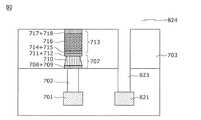
図28は、特許文献1に開示されている、パンチスルーダイオードと直列に接続されたプログラマブル抵抗器を有する従来の不揮発性記憶素子70の断面図である。 FIG. 28 is a cross-sectional view of a conventional
従来の不揮発性記憶素子70は、銅ダマシン技術を用いて以下のように形成される。 The conventional
まず、銅メタライゼーション層701及び、対応するプラグ702が仕上げられる。次いで、第1の積層体707が、バリア層708、コンタクト層709、半導体層710、コンタクト層711、及びバリア層712の堆積によって形成される。その後、バリア層714、電極層715、PMC材料716、コンタクト層717、及びバリア層718からなる、第2の積層体713が堆積される。第1の積層体707、第2の積層体713はパターニングされ、それぞれパンチスルーダイオード(以下、ダイオード素子707)、プログラマブル抵抗器(抵抗変化素子713)が形成される。次いで、金属間誘電体層が堆積され、誘電体CMPにより、金属間誘電体層の表面は平坦化される。その後、IMD層703が堆積され、トレンチ704がエッチングされ、トレンチ704はバリア層705及び、銅によって充填され、それに銅CMPが後続する。このようにして、銅相互接続層706が形成される。 First, the
従来の不揮発性記憶装置では、図28に示されるような構成に加えて、典型的には、引き出しコンタクトプラグと該引き出しコンタクトプラグに接続された他の配線層とを有する。図29は、図28に示される不揮発性記憶素子70に加えて、他の配線層である銅メタライゼーション層821および引き出しコンタクトプラグ822を備える不揮発性記憶装置80の一例を示している。 In addition to the configuration shown in FIG. 28, the conventional nonvolatile memory device typically has a lead contact plug and another wiring layer connected to the lead contact plug. FIG. 29 shows an example of a
しかしながら、後述するように、引き出しコンタクトプラグ822と、引き出しコンタクトプラグ822上の配線である銅相互接続層706とを同一工程で埋め込む場合、当該埋め込み工程前に行われる工程によって抵抗変化素子713、ダイオード素子707、またはその両方の電気的特性が劣化する問題があることに、発明者らは気付いた。この問題については、後ほど詳述する。 However, as will be described later, when the
本発明は、上記の課題を解決するためになされたものであり、プラグと配線の電気的接触を良好に保ち、抵抗変化素子、ダイオード素子、またはその両方の電気的特性のばらつき又は劣化を抑制する不揮発性記憶素子及び不揮発性記憶装置、並びにそれらの製造方法を提供することを目的とする。 The present invention has been made to solve the above-described problems, and maintains good electrical contact between the plug and the wiring, and suppresses variation or deterioration in electrical characteristics of the variable resistance element, the diode element, or both. An object of the present invention is to provide a nonvolatile memory element, a nonvolatile memory device, and a manufacturing method thereof.
上記目的を達成するために、本発明の一形態に係る不揮発性記憶素子の製造方法は、第1の配線を形成する第1工程と、前記第1の配線上に第1の層間絶縁層を形成し、前記第1の層間絶縁層中に、前記第1の配線に電気的に接続される第1のプラグ及び第2のプラグを、前記第1のプラグ及び第2のプラグの上面が略同一平面内になるように形成する第2工程と、前記第1のプラグ上に、第1電極と第2電極と抵抗変化層とを有し、前記第1電極が前記第1のプラグと電気的に接続されている抵抗変化素子を形成する第3工程と、前記抵抗変化素子及び前記第1の層間絶縁層上に第2の層間絶縁層を形成し、前記第2の層間絶縁層中に前記第2電極に電気的に接続される第2の配線と前記第2のプラグに電気的に接続される第3の配線とを、前記第2の配線及び前記第3の配線の上面が略同一平面内になるように形成する第4工程とを含む。 In order to achieve the above object, a method for manufacturing a nonvolatile memory element according to one embodiment of the present invention includes a first step of forming a first wiring, and a first interlayer insulating layer over the first wiring. The first plug and the second plug electrically connected to the first wiring are formed in the first interlayer insulating layer, and the upper surfaces of the first plug and the second plug are substantially the same. A second step of forming the first plug so as to be in the same plane; and a first electrode, a second electrode, and a resistance change layer on the first plug, wherein the first electrode is electrically connected to the first plug. A third step of forming a resistance change element connected to each other, a second interlayer insulating layer is formed on the resistance change element and the first interlayer insulating layer, and the second interlayer insulating layer is formed in the second interlayer insulating layer A second wiring electrically connected to the second electrode and a third wiring electrically connected to the second plug; And a fourth step of the upper surface of the second wiring and the third wiring is formed to be in substantially the same plane.
このような製造方法により、前記第4工程において、第2の配線及び第3の配線を埋め込み形成する際に、第1の配線と第3の配線を接続する引き出しコンタクトプラグとして機能する第2のプラグがあらかじめ形成されているため、プラグと配線の電気的接触を良好に保ち、かつ、抵抗変化素子の形成後にプラグと配線の電気的接触を向上させる加工を行った場合に生じ得る抵抗変化素子の電気的特性の劣化を抑制し、素子間のばらつきを低減することができる。 With such a manufacturing method, the second wiring functioning as a lead contact plug for connecting the first wiring and the third wiring when the second wiring and the third wiring are embedded and formed in the fourth step. Since the plug is formed in advance, the resistance change element that can be generated when processing for improving the electrical contact between the plug and the wiring after the formation of the resistance change element is performed after the resistance change element is formed. It is possible to suppress the deterioration of the electrical characteristics of the device and reduce the variation between elements.
また、前記第3工程において、前記第1電極と前記抵抗変化層との間に、前記第1電極に電気的に接続される半導体層と、前記半導体層と前記抵抗変化層とに挟持される中間電極とを形成し、前記第1電極と前記半導体層と前記中間電極とは、ダイオード素子を構成し、前記中間電極と前記抵抗変化層と前記第2電極とは、前記抵抗変化素子を構成してもよい。 Further, in the third step, the semiconductor layer electrically connected to the first electrode, and the semiconductor layer and the resistance change layer are sandwiched between the first electrode and the resistance change layer. An intermediate electrode is formed, the first electrode, the semiconductor layer, and the intermediate electrode constitute a diode element, and the intermediate electrode, the resistance change layer, and the second electrode constitute the resistance change element. May be.
このような製造方法により、第2の配線と半導体層の接触面積は、第2の電極と半導体層の接触面積に比べて大きくなるので、第2の配線の周囲にまで電気力線が広がって、ダイオード素子の電流容量を高くすることができ、抵抗変化素子の抵抗変化時に必要な大電流密度の電流を流すことができるクロスポイント型の不揮発性記憶素子を製造できる。 With such a manufacturing method, the contact area between the second wiring and the semiconductor layer is larger than the contact area between the second electrode and the semiconductor layer, so that the lines of electric force spread to the periphery of the second wiring. Thus, it is possible to manufacture a cross-point type nonvolatile memory element that can increase the current capacity of the diode element and can flow a current having a large current density required when the resistance of the variable resistance element changes.
また、前記不揮発性記憶素子の製造方法は、前記第3工程の後かつ前記第4工程の前に、前記抵抗変化素子を構成する少なくとも前記抵抗変化層の側壁を被覆し、絶縁性かつ酸素バリア性を有する保護層を形成する第5工程を含んでもよい。 In addition, the method for manufacturing the nonvolatile memory element includes: after the third step and before the fourth step, covering at least a side wall of the variable resistance layer constituting the variable resistance element; A fifth step of forming a protective layer having properties may be included.
このような製造方法により、第5工程において、抵抗変化層の側壁が保護層によって予め被覆される。そのため、第4工程において、抵抗変化素子を含む第1の層間絶縁層上に第2の層間絶縁層をCVD法などを用いて堆積する際に、酸素プラズマや熱によって抵抗変化層が酸化することを防止できる。さらに、層間絶縁層堆積後の熱処理によって層間絶縁層中に含まれる酸素が拡散し、抵抗変化層の側壁から酸化が進行することも防止できる。 By such a manufacturing method, the side wall of the resistance change layer is previously covered with the protective layer in the fifth step. Therefore, in the fourth step, when the second interlayer insulating layer is deposited on the first interlayer insulating layer including the variable resistance element by using the CVD method, the variable resistance layer is oxidized by oxygen plasma or heat. Can be prevented. Furthermore, it is possible to prevent the oxygen contained in the interlayer insulating layer from diffusing due to the heat treatment after the interlayer insulating layer is deposited, and the oxidation from proceeding from the sidewall of the resistance change layer.
また、第4工程において、第2の配線を埋め込み形成するための配線溝を形成する際に、配線溝内に抵抗変化層が露出することを防止でき、第2の配線と抵抗変化層との間にリークパスが形成されることを防止できる。抵抗変化層は、第1電極と第2電極との間に与えられる電気的信号によって高抵抗状態と低抵抗状態との間を可逆的に動作するため、第1電極を介さずに抵抗変化層へ電流が流れるリークパスが形成されると、動作不良が発生するが、抵抗変化層の側壁を保護層によって被覆することによって、この抵抗変化動作不良の発生を防止できる。 Further, in the fourth step, when the wiring groove for embedding the second wiring is formed, the resistance change layer can be prevented from being exposed in the wiring groove, and the second wiring and the resistance change layer can be prevented from being exposed. It is possible to prevent a leak path from being formed between them. Since the resistance change layer reversibly operates between the high resistance state and the low resistance state by an electrical signal applied between the first electrode and the second electrode, the resistance change layer does not pass through the first electrode. When a leak path through which a current flows is formed, an operation failure occurs. However, the resistance change operation failure can be prevented by covering the side wall of the resistance change layer with a protective layer.
さらに、第5工程において、抵抗変化素子の側壁が保護層によって予め被覆されるため、第4工程において、第2電極と接続する第2の配線を埋め込み形成するための配線溝が深く掘れ込んでも配線溝内に抵抗変化層が露出することを防止できる。そのため、第2の配線を埋め込み形成するための配線溝と、それよりも深い第3の配線を埋め込み形成するための配線溝とを同時にドライエッチングによって形成することができる。 Further, in the fifth step, since the sidewall of the resistance change element is previously covered with the protective layer, even in the fourth step, the wiring groove for embedding and forming the second wiring connected to the second electrode is deeply dug. It is possible to prevent the resistance change layer from being exposed in the wiring trench. Therefore, the wiring groove for embedding the second wiring and the wiring groove for embedding the third wiring deeper than that can be simultaneously formed by dry etching.
また、前記第5工程において、前記抵抗変化素子を含む前記第1の層間絶縁層上に前記保護層を堆積させ、前記抵抗変化素子の側壁部分以外の前記保護層を除去してもよい。 In the fifth step, the protective layer may be deposited on the first interlayer insulating layer including the variable resistance element, and the protective layer other than the sidewall portion of the variable resistance element may be removed.
このような製造方法により、保護層が複数の抵抗変化素子ごとに分離して形成される。これにより、抵抗変化素子が形成されていない領域には、保護層が存在しない。したがって、抵抗変化素子を設けていない領域に、第2のプラグと接続する第3の配線を埋め込み形成するための配線溝を形成する際のドライエッチング工程が容易になる。 By such a manufacturing method, the protective layer is formed separately for each of the plurality of resistance change elements. Thereby, the protective layer does not exist in the region where the variable resistance element is not formed. Therefore, the dry etching process when forming the wiring trench for embedding and forming the third wiring connected to the second plug in the region where the variable resistance element is not provided is facilitated.
また、前記第4工程において、前記第2電極と前記第2の配線とに挟持され、前記第2電極に電気的に接続される半導体層を形成し、前記第2電極と前記半導体層と前記第2の配線とは、ダイオード素子を構成してもよい。 In the fourth step, a semiconductor layer sandwiched between the second electrode and the second wiring and electrically connected to the second electrode is formed, and the second electrode, the semiconductor layer, The second wiring may constitute a diode element.
このような製造方法により、トランジスタ等のスイッチング素子を配置することなく、大容量かつ高集積化が可能なクロスポイント型の不揮発性記憶素子を製造できる。 With such a manufacturing method, a cross-point type nonvolatile memory element capable of high capacity and high integration can be manufactured without arranging switching elements such as transistors.
また、前記第1工程において、前記第1の配線を銅で構成してもよい。 In the first step, the first wiring may be made of copper.
このような製造方法は、半導体装置の製造に広く用いられている銅ダマシンプロセスとの親和性に優れる。 Such a manufacturing method is excellent in affinity with a copper damascene process widely used for manufacturing semiconductor devices.
また、上記目的を達成するために、本発明の一形態に係る不揮発性記憶装置の製造方法は、第1方向に延びる複数の第1の配線を設ける第1工程と、前記複数の第1の配線上に第1の層間絶縁層を形成し、前記第1の層間絶縁層中に、各々が前記複数の第1の配線のうちのいずれか1つに電気的に接続される複数の第1のプラグ及び複数の第2のプラグを、前記複数の第1のプラグ及び複数の第2のプラグの上面が略同一平面内になるように形成する第2工程と、前記複数の第1のプラグ上に、各々が、第1電極と第2電極と抵抗変化層とを有し、前記第1電極が前記複数の第1のプラグのうちのいずれか1つと電気的に接続されている複数の抵抗変化素子を形成する第3工程と、前記複数の抵抗変化素子及び前記第1の層間絶縁層上に第2の層間絶縁層を形成し、前記第2の層間絶縁層中に、各々が複数の前記抵抗変化素子の前記第2電極と電気的に接続される複数の第2の配線と、前記複数の第2のプラグと電気的に接続される第3の配線とを、前記複数の第2の配線及び前記第3の配線の上面が略同一平面内にあって、前記第1方向と交差する第2方向に延びるように形成する第4工程とを含む。 In order to achieve the above object, a method for manufacturing a nonvolatile memory device according to an aspect of the present invention includes a first step of providing a plurality of first wirings extending in a first direction, and the plurality of first A first interlayer insulating layer is formed on the wiring, and a plurality of first layers each electrically connected to any one of the plurality of first wirings in the first interlayer insulating layer. A second step of forming the plurality of first plugs and the plurality of second plugs such that upper surfaces of the plurality of first plugs and the plurality of second plugs are substantially in the same plane; and the plurality of first plugs A plurality of first electrodes, a second electrode, and a resistance change layer, wherein the first electrode is electrically connected to any one of the plurality of first plugs; A third step of forming a resistance change element; and a second step on the plurality of resistance change elements and the first interlayer insulating layer. An interlayer insulating layer is formed, and in the second interlayer insulating layer, a plurality of second wirings that are electrically connected to the second electrodes of the plurality of resistance change elements, and the plurality of second wirings A third wiring electrically connected to the plug of the second wiring in a second direction intersecting the first direction, wherein the plurality of second wirings and the upper surface of the third wiring are substantially in the same plane. And a fourth step of forming so as to extend.
また、前記不揮発性記憶装置の製造方法は、各々が、半導体層を含んで構成されかつ前記複数の抵抗変化素子のうちの対応する抵抗変化素子と電気的に接続されている複数のダイオード素子を形成する第5工程をさらに含んでもよい。 The method for manufacturing the nonvolatile memory device includes a plurality of diode elements each including a semiconductor layer and electrically connected to a corresponding resistance change element among the plurality of resistance change elements. You may further include the 5th process to form.
また、前記第1工程において、前記第1の配線を銅で構成してもよい。 In the first step, the first wiring may be made of copper.
このような製造方法により、前記第4工程をにおいて、複数の第2の配線及び第3の配線を埋め込み形成する際に、複数の第1の配線と第3の配線を接続する引き出しコンタクトプラグとして機能する複数の第2のプラグがあらかじめ形成されているため、プラグと配線の電気的接触を良好に保ち、かつ、抵抗変化素子の形成後にプラグと配線の電気的接触を向上させる加工を行った場合に生じ得る抵抗変化素子の電気的特性の劣化を抑制し、素子間のばらつきを低減することができる。 With such a manufacturing method, when the plurality of second wirings and the third wiring are embedded and formed in the fourth step, the lead contact plugs connect the plurality of first wirings and the third wirings. Since a plurality of functioning second plugs are formed in advance, the electrical contact between the plug and the wiring is kept good, and after the resistance change element is formed, the electrical contact between the plug and the wiring is improved. It is possible to suppress deterioration of electrical characteristics of the variable resistance element that may occur in some cases, and to reduce variations between elements.
上記目的を達成するために、本発明の一形態に係る不揮発性記憶素子は、第1の配線と、前記第1の配線上に形成され、前記第1の配線に接続される第1のプラグ及び第2のプラグと、第1電極、第2電極、及び前記第1電極と前記第2電極とに挟持され前記第1電極と前記第2電極との間に与えられる電気的信号に基づいて高抵抗状態と前記高抵抗状態より抵抗値が低い低抵抗状態との間を可逆的に変化する抵抗変化層を有し、前記第1のプラグ上に形成され、前記第1電極が前記第1のプラグと電気的に接続されている抵抗変化素子と、前記抵抗変化素子上に形成され、前記第2電極と電気的に接続されている第2の配線と、前記第2のプラグ上に形成され、前記第2のプラグと電気的に接続されている第3の配線とを備え、前記第1のプラグの上面と前記第2のプラグの上面とが略同一平面内に形成され、かつ前記第2の配線の上面と前記第3の配線の上面とが略同一平面内に形成されている。ここで、上面とは、対象とする部材が有する表面のうち、基板から最も遠い面を意味する。 To achieve the above object, a nonvolatile memory element according to one embodiment of the present invention includes a first wiring and a first plug formed over the first wiring and connected to the first wiring. And the second plug, the first electrode, the second electrode, and the electrical signal sandwiched between the first electrode and the second electrode and applied between the first electrode and the second electrode. A resistance change layer that reversibly changes between a high resistance state and a low resistance state having a resistance value lower than that of the high resistance state; and formed on the first plug, wherein the first electrode is the first electrode. A variable resistance element electrically connected to the plug, a second wiring formed on the variable resistance element and electrically connected to the second electrode, and formed on the second plug. And a third wiring electrically connected to the second plug, the first plug The upper surface of the lug and the upper surface of the second plug is formed in substantially the same plane, and the upper surface of the second wiring and the upper surface of the third wiring is formed in substantially the same plane. Here, the upper surface means a surface farthest from the substrate among the surfaces of the target member.
このような構成とすることにより、第3の配線の膜厚は、第2の配線の膜厚に比べて厚いため、配線抵抗を下げることができ、集積度の向上により第3の配線の配線長が長くなる場合に、配線遅延の影響が小さく、高速動作可能な不揮発性記憶素子を実現できる。 By adopting such a configuration, the thickness of the third wiring is thicker than the thickness of the second wiring, so that the wiring resistance can be lowered and the wiring of the third wiring can be improved by increasing the degree of integration. When the length is long, a nonvolatile memory element that is less affected by wiring delay and can operate at high speed can be realized.
また、前記第1のプラグ及び第2のプラグがタングステン又は銅のいずれかを含む導電材料から構成されていてもよい。導電材料には、特に、タングステンを用いることが好ましい。 The first plug and the second plug may be made of a conductive material containing either tungsten or copper. In particular, tungsten is preferably used as the conductive material.
このような構成とすることにより、特にプラグが銅よりも酸化しにくいタングステンから構成される場合、第1のプラグと抵抗変化素子及び、第2のプラグと第3の配線との電気的コンタクトが良好な不揮発性記憶素子を実現できる。 With such a configuration, particularly when the plug is made of tungsten that is less likely to be oxidized than copper, the first plug and the resistance change element, and the second plug and the third wiring are in electrical contact with each other. A good nonvolatile memory element can be realized.
また、前記抵抗変化層は、酸素不足型タンタル酸化物、酸素不足型ハフニウム酸化物、及び酸素不足型ジルコニウム酸化物のうちの1つ以上を含んでもよい。 The resistance change layer may include one or more of oxygen-deficient tantalum oxide, oxygen-deficient hafnium oxide, and oxygen-deficient zirconium oxide.
このような構成とすることにより、動作の高速性に加えて可逆的に安定した書き換え特性と良好な抵抗値のリテンション特性を有する不揮発性記憶素子を製造することができる。特に、タンタル酸化物を用いた場合には、通常のSi半導体プロセスと親和性の高い製造プロセスで製造できる。 With such a configuration, a nonvolatile memory element having reversibly stable rewriting characteristics and good resistance retention characteristics in addition to high-speed operation can be manufactured. In particular, when tantalum oxide is used, it can be manufactured by a manufacturing process having high affinity with a normal Si semiconductor process.
また、前記抵抗変化層は、第1の遷移金属酸化物で構成されている第1の抵抗変化層と、遷移金属酸化物で構成されており、第1の抵抗変化層より酸素不足度が小さい第2の遷移金属酸化物で構成される第2の抵抗変化層とを有してもよい。 The variable resistance layer includes a first variable resistance layer made of a first transition metal oxide and a transition metal oxide, and has a lower oxygen deficiency than the first variable resistance layer. You may have a 2nd resistance change layer comprised with a 2nd transition metal oxide.
このような構成とすることにより、抵抗変化層を酸素不足度が異なる遷移金属酸化物からなる積層構成にすることによって、抵抗変化する極性が常に安定することで、不揮発性記憶素子として安定な動作特性を得ることができる。 By adopting such a configuration, the resistance change layer is made of a laminated structure made of transition metal oxides having different degrees of oxygen deficiency, so that the polarity of resistance change is always stable, so that stable operation as a nonvolatile memory element is achieved. Characteristics can be obtained.
また、前記不揮発性記憶素子は、前記抵抗変化素子を構成する前記抵抗変化層の側壁を被覆し、絶縁性かつ酸素バリア性を有する保護層をさらに備えてもよい。ここで、抵抗変化素子の側壁とは、抵抗変化層が有する面のうち、第1電極と接する面および第2電極と接する面以外の面を意味する。 The nonvolatile memory element may further include a protective layer that covers the sidewall of the variable resistance layer constituting the variable resistance element and has an insulating property and an oxygen barrier property. Here, the side wall of the resistance change element means a surface other than the surface in contact with the first electrode and the surface in contact with the second electrode among the surfaces of the resistance change layer.
このような構成とすることにより、抵抗変化素子形成後の製造工程における層間絶縁層の成膜工程及び熱処理工程によって、抵抗変化層の側面からの酸化を抑制することができる。これにより、抵抗変化層の実効的な断面積がばらつくことを抑制できる。 With such a configuration, oxidation from the side surface of the resistance change layer can be suppressed by the film formation process and heat treatment process of the interlayer insulating layer in the manufacturing process after the resistance change element is formed. Thereby, it can suppress that the effective cross-sectional area of a resistance change layer varies.
さらに、第2の配線を形成する工程において、第2の配線と抵抗変化層との間にリークパスが形成されることを防止できる。 Furthermore, it is possible to prevent a leak path from being formed between the second wiring and the resistance change layer in the step of forming the second wiring.
また、前記第2電極は貴金属から構成されていてもよい。 The second electrode may be made of a noble metal.
このような構成とすることにより、より酸化されやすい材料で前記第2電極を構成した場合に必要となる、前記第2電極に形成された表面酸化膜を除去するためのプリクリーン処理を低減もしくは省略できる。その結果、当該プリクリーンを行った場合に生じる前記第2電極の膜減りや、前記抵抗変化素子へのダメージが低減もしくは防止され、抵抗変化素子の特性ばらつきが低減される。 With such a configuration, the preclean process for removing the surface oxide film formed on the second electrode, which is necessary when the second electrode is configured with a material that is more easily oxidized, is reduced or Can be omitted. As a result, film loss of the second electrode and damage to the variable resistance element that occur when the preclean is performed are reduced or prevented, and characteristic variation of the variable resistance element is reduced.
また、上記目的を達成するために、本発明の一形態に係る不揮発性記憶装置は、第1方向に延びる複数の第1の配線と、前記複数の第1の配線上に配置され、各々が、前記複数の第1の配線のうちのいずれか1つと電気的に接続されている、複数の第1のプラグと、前記複数の第1の配線上に配置され、各々が、前記複数の第1の配線のうちのいずれか1つと電気的に接続されている、複数の第2のプラグと、前記複数の第1のプラグ上に配置され、各々が、第1電極、第2電極、及び前記第1電極と前記第2電極とに挟持され前記第1電極と前記第2電極との間に与えられる電気的信号に基づいて高抵抗状態と前記高抵抗状態より抵抗値が低い低抵抗状態との間を可逆的に変化する抵抗変化層を有し、前記第1電極が前記複数の第1プラグのうちのいずれか1つと電気的に接続されている複数の抵抗変化素子と、前記複数の抵抗変化素子上に前記第1方向と交差する第2方向に延び、各々が、複数の抵抗変化素子の前記第2電極と電気的に接続されている複数の第2の配線と、前記複数の第2のプラグ上に前記第2方向に延び、前記複数の第2のプラグと電気的に接続されている第3の配線とを備え、前記複数の第1のプラグの上面と前記複数の第2のプラグの上面とが略同一平面内にあり、かつ前記複数の第2の配線の上面と前記複数の第3の配線の上面とが略同一平面内にある。 In order to achieve the above object, a nonvolatile memory device according to one embodiment of the present invention is provided over a plurality of first wirings extending in a first direction and the plurality of first wirings, each of which is A plurality of first plugs electrically connected to any one of the plurality of first wirings and the plurality of first wirings, each of which is disposed on the plurality of first wirings. A plurality of second plugs electrically connected to any one of the first wirings, and disposed on the plurality of first plugs, each comprising a first electrode, a second electrode, and A low resistance state having a resistance value lower than that of the high resistance state and the high resistance state based on an electrical signal sandwiched between the first electrode and the second electrode and applied between the first electrode and the second electrode A variable resistance layer that reversibly changes between the first plug and the first electrode. A plurality of resistance change elements electrically connected to any one of the plurality of resistance change elements; and a plurality of resistance change elements extending in a second direction intersecting the first direction on the plurality of resistance change elements. A plurality of second wirings electrically connected to the second electrode; and a plurality of second wirings extending in the second direction on the plurality of second plugs and electrically connected to the plurality of second plugs. The upper surfaces of the plurality of first plugs and the upper surfaces of the plurality of second plugs are in substantially the same plane, and the upper surfaces of the plurality of second wires and the plurality of second plugs The upper surface of the third wiring is substantially in the same plane.
また、前述の不揮発性記憶装置は、各々が、半導体層を含んで構成され、かつ前記複数の抵抗変化素子のうちのいずれか1つと電気的に接続されている、複数のダイオード素子をさらに備えてもよい。 The nonvolatile memory device further includes a plurality of diode elements each including a semiconductor layer and electrically connected to any one of the plurality of resistance change elements. May be.
また、前述の半導体層は、窒素不足型シリコン窒化物を含んでもよい。 The semiconductor layer described above may include nitrogen-deficient silicon nitride.
このような構成とすることにより、抵抗変化動作を安定にすることに加えて、漏れ電流を低減でき、大容量で高集積可能なクロスポイントメモリ型の不揮発性記憶装置を提供することができる。 With such a configuration, in addition to stabilizing the resistance change operation, it is possible to provide a cross-point memory type nonvolatile memory device that can reduce leakage current and can be integrated with a large capacity.
なお、本明細書では、ダイオード素子を、印加電圧が臨界電圧以下では電気抵抗が非常に高く、その一方で、臨界電圧を超えると電気抵抗が急激に低下することで大電流が流れるという非線形の電気抵抗特性を有する二端子素子と定義する。このような特性を備える二端子素子としては、例えば、MSM(Metal−Semiconductor−Metal)ダイオード、MIM(Metal−Insulator−Metal)ダイオード、あるいは、バリスタ等が知られている。 In the present specification, the diode element has a non-linearity in which the electric resistance is very high when the applied voltage is lower than the critical voltage, and on the other hand, when the voltage exceeds the critical voltage, the electric resistance sharply decreases and a large current flows. It is defined as a two-terminal element having electrical resistance characteristics. As a two-terminal element having such characteristics, for example, an MSM (Metal-Semiconductor-Metal) diode, an MIM (Metal-Insulator-Metal) diode, or a varistor is known.
なお、本発明は、このような不揮発性記憶素子及び不揮発性記憶装置並びにそれらの製造方法として実現できるだけでなく、このような不揮発性記憶素子を実現する半導体集積回路(LSI)として実現することができる。 The present invention can be realized not only as such a nonvolatile memory element, a nonvolatile memory device, and a manufacturing method thereof, but also as a semiconductor integrated circuit (LSI) that realizes such a nonvolatile memory element. it can.
なお、本発明は、抵抗変化素子が酸素不足型の遷移金属酸化物を含む抵抗変化層を備えるReRAMで構成されている例を説明したが、当該抵抗変化素子は、電気的信号に基づいて、高抵抗状態と前記高抵抗状態より抵抗値が低い低抵抗状態との間を可逆的に変化する素子であればよいので、例えば、強誘電体のヒステリシス(履歴現象)を利用し正負の自発分極を1と0に対応させた強誘電体メモリ(FeRAM:Ferroelectric RAM)や相変化材料を用いた相変化メモリ(PCRAM:Phase−Change RAM)及び、記憶素子に磁性体を用い、書き込み方式にスピン注入磁化反転を採用する磁気抵抗メモリ(MRAM:Magnetoresistive RAM)などであってもよい。 In the present invention, the example in which the variable resistance element is configured by a ReRAM including a variable resistance layer including an oxygen-deficient transition metal oxide has been described. However, the variable resistance element is based on an electrical signal. Any element that reversibly changes between a high-resistance state and a low-resistance state having a resistance value lower than that of the high-resistance state can be used. For example, positive and negative spontaneous polarization using the hysteresis (history phenomenon) of a ferroelectric substance A ferroelectric memory (FeRAM: Ferroelectric RAM) corresponding to 1 and 0, a phase change memory (PCRAM: Phase-Change RAM) using a phase change material, and a magnetic material for a storage element, and a spin for a writing method. It may be a magnetoresistive memory (MRAM: Magnetoresistive RAM) that employs injection magnetization reversal.
以上説明したように、本発明は、抵抗変化素子を含む不揮発性記憶素子において、良好な電気的特性が得られるデバイス構造を有する不揮発性記憶素子及び不揮発性記憶装置、並びにそれらの製造方法を提供できる。 As described above, the present invention provides a nonvolatile memory element and a nonvolatile memory device having a device structure capable of obtaining good electrical characteristics in a nonvolatile memory element including a resistance change element, and a method for manufacturing the same. it can.
本発明者らは、良好な電気的特性が得られる不揮発性記憶装置の製造方法について検討を重ねた結果、従来の不揮発性記憶装置において、以下の課題があることを見出し、本発明を完成した。以下では、図28から図30に示される例を用いて、従来の不揮発性記憶装置における課題について説明する。ただし、これらの図を用いるのは課題の一例を具体的に説明するためであり、本発明の課題は、これらの構造および材料等、および以下で説明する具体的なプロセスに限定された不揮発性記憶装置においてのみ生じるものではない。 As a result of studying a manufacturing method of a nonvolatile memory device that can obtain good electrical characteristics, the present inventors have found that the conventional nonvolatile memory device has the following problems, and have completed the present invention. . Hereinafter, problems in the conventional nonvolatile memory device will be described using the examples shown in FIGS. However, these drawings are used to specifically describe an example of the problem, and the problem of the present invention is nonvolatile that is limited to these structures and materials, and a specific process described below. It does not occur only in storage devices.
図29は、従来の不揮発性記憶装置80の一例を示している。不揮発性記憶装置80は、銅メタライゼーション層701と同じ層に他の銅メタライゼーション層821が形成されており、当該銅メタライゼーション層821と銅相互接続層706とを接続する引き出しコンタクトプラグ822が形成されている。 FIG. 29 shows an example of a conventional
図29に示される引き出しコンタクトプラグ822および銅相互接続層706は、典型的には以下のプロセスで形成される。 The
まず、図30に示されるように、フォトリソグラフィー及びドライエッチングによって、引き出しコンタクトプラグ822を埋め込むためのコンタクトホール823、及び銅配線を埋め込むためのトレンチ824(配線溝)が形成される。なお、図29に示される第3のIMD層703の上面は、配線溝の底面を示しており、トレンチ824は紙面に対して平行に形成されるものとしている。 First, as shown in FIG. 30, a
次に、そのコンタクトホール823及びトレンチ824内にバリア層705と、配線材料のシード層となる銅とを、スパッタ法等を用いて堆積させる。次いで、電解めっき法等により、銅のシード層上に銅をさらに堆積させることで、コンタクトホール823とトレンチ824を全て配線材料の銅で充填する。その後、堆積した銅のうち表面の余分な銅をCMP(Chemical Mechanical Polishing)法によって除去する。 Next, a
以上の工程によって、銅相互接続層706及び、引き出しコンタクトプラグ822が形成される。 Through the above steps, the
しかしながら、図29に示す不揮発性記憶装置80における引き出しコンタクトプラグ822を上述のようなプロセスで形成する際には以下に述べる課題が生じる。 However, when the
コンタクトホール823及びトレンチ824を形成する際、コンタクトホール823の底部に露出する銅メタライゼーション層821の表面が、酸化される。具体的には、配線材料が、ドライエッチングに用いられるエッチングガスや、その後のフォトレジスト除去のためのアッシング処理に用いられる酸素ガス、さらに洗浄工程に用いられる薬液に曝されることによって酸化される。 When the
この銅メタライゼーション層821の表面に形成された酸化膜は、一般的には、アルゴンプラズマを用いたプリクリーン処理や、水素プラズマによる還元処理などの前工程によって除去される。これにより、銅メタライゼーション層821と引き出しコンタクトプラグ822との電気的な接続を高めることができる。 The oxide film formed on the surface of the
しかし、この表面酸化膜の除去処理では、コンタクトホール823底部に露出している銅メタライゼーション層821のみでなく、トレンチ824の底部に露出している第2の積層体713の表面(コンタクト層717、及びバリア層718)も、除去処理用のガス等に曝される。そのため、第2の積層体713の表面がリスパッタされ、スパッタされた材料がコンタクトホール823の側壁やトレンチ704の側壁に堆積することで、バリア層705の膜剥がれやカバレッジ不良などによる銅相互接続層706の信頼性の劣化を引き起こすおそれがある。 However, in this surface oxide film removal process, not only the
また、この表面酸化膜の除去処理にプラズマが用いられることにより、抵抗変化素子713とダイオード素子707とで構成されるメモリセルを複数形成したときに、抵抗変化素子713の初期状態がメモリセル間でばらつくことがある。これは、例えば、IMD層703表面に電荷が蓄積されることによって、抵抗変化素子713に電流が流れ、製造工程中に抵抗変化素子713に意図しない書き込みが行われることによって生じる。 In addition, since plasma is used for the removal process of the surface oxide film, when a plurality of memory cells including the
さらに、このようなプラズマ処理によって、抵抗変化素子713を介して、ダイオード707にも電流が流れ、ダイオード破壊を引き起こすことがある。 Further, such plasma treatment may cause a current to flow to the
また、図30に示される例ではダイオード素子707の上に抵抗変化素子713が形成されている例について説明したが、抵抗変化素子713の上にダイオード素子707が形成されている場合についても同様の課題が生じる。 In the example shown in FIG. 30, the example in which the
以上より、従来の不揮発性記憶装置80は、銅メタライゼーション層821と引き出しコンタクトプラグ822との電気的接触の向上と、抵抗変化素子713、ダイオード素子707、及びその両方のばらつき抑制との両立が困難であるという課題を有している。 As described above, the conventional
本発明は、上記課題を解決するためになされたものである。 The present invention has been made to solve the above problems.
以下、本発明の実施の形態に係る抵抗変化型の不揮発性記憶素子(以下、単に不揮発性記憶素子とも言う)とその製造方法について、図面を参照しながら説明する。なお、図面において、同じ符号が付いたものは、説明を省略する場合がある。また、図面は理解しやすくするために、それぞれの構成要素を模式的に示したもので、形状及び寸法などについては正確な表示ではない。 Hereinafter, a variable resistance nonvolatile memory element (hereinafter also simply referred to as a nonvolatile memory element) and a manufacturing method thereof according to an embodiment of the present invention will be described with reference to the drawings. In the drawings, the description with the same reference numerals may be omitted. In addition, the drawings schematically show each component for easy understanding, and shapes and dimensions are not accurate.
(実施の形態1)
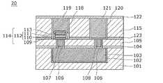
図1は、本発明の実施の形態1に係る不揮発性記憶素子10の構成例を示す断面図である。(Embodiment 1)
FIG. 1 is a cross-sectional view showing a configuration example of the
図1では、一般的な半導体記憶装置においてメモリセルアレイ又はメモリ本体部などと呼ばれる領域の一部分が、不揮発性記憶素子10として示されている。すなわち、半導体記憶装置はメモリセルアレイを備え、メモリセルアレイは不揮発性記憶素子10から構成される。また、不揮発性記憶素子は、抵抗変化素子114を含む。なお、半導体記憶装置は、このような不揮発性記憶素子10を含むメモリセルアレイとともに、メモリセルアレイを駆動するための図示しない駆動回路を備えていてもよい。 In FIG. 1, a part of a region called a memory cell array or a memory main body in a general semiconductor memory device is shown as a
駆動回路は、メモリセルアレイ中の不揮発性記憶素子10に電気パルスを印加する。不揮発性記憶素子10の抵抗変化素子114の抵抗状態は、データ書き込み用の電気パルスの印加によって変更される。また、不揮発性記憶素子10の抵抗変化素子114の抵抗状態は、データ読み出し用の電気パルスの印加によって読み出される。 The drive circuit applies an electric pulse to the
第1の層間絶縁層101は、トランジスタなどが形成されている半導体基板(図示せず)上に形成されており、例えば、シリコン酸化物で構成される。 The first
第1の配線103は、第1の層間絶縁層101中に形成されており、第1の層間絶縁層101と第1の配線103との間には、第1のバリアメタル層102が設けられている。なお、第1の配線103は、望ましくは、銅から構成される。 The
第1のライナー層104は、第1の配線103を含む第1の層間絶縁層101上に形成されており、例えば、シリコン窒化物(例えば、膜厚30〜200nm)で構成される。 The
第2の層間絶縁層105は、第1のライナー層104上に形成されており、例えば、シリコン酸化物(例えば、膜厚100〜500nm)で構成される。 The second
第1のプラグ107及び第2のプラグ108(例えば、直径50〜200nm)は、第1のライナー層104及び第2の層間絶縁層105中に形成されている。第1のプラグ107及び第2のプラグ108は、導電性材料で形成された第2のバリアメタル層106を介して、第1の配線103と電気的に接続されている。 The
なお、本明細書中において「電気的に接続されている」とは、接続されている2つの部材が常に導通していることを意味する。したがって、例えば、接続されている2つの部材の間にバリアメタルが介在する場合、それら2つの部材は電気的に接続されている。すなわち、上記の例において、第1のプラグ107及び第2のプラグ108は、第1の配線103と電気的に接続されている。一方、例えば、接続されている2つの部材の間に抵抗変化素子やダイオード素子等が介在する場合、それら2つの部材は電気的に接続されていない。なお、以下では、「電気的に接続されている」ことを単に「接続されている」ということがある。 In the present specification, “electrically connected” means that two connected members are always in conduction. Therefore, for example, when a barrier metal is interposed between two connected members, the two members are electrically connected. That is, in the above example, the
第1のプラグ107の上面と第2のプラグ108の上面とは略同一平面内に形成されている。ここで、略同一平面とは、例えばCMP法によって形成される程度に平坦な平面を指しており、例えば100nm以下の凹凸を有する面を略同一平面と定義する。略同一平面の定義は、半導体プロセスの違い(例えばデザインルール)によって異なる。 The upper surface of the
抵抗変化素子114は、第2の層間絶縁層105上に形成されるとともに、第1のプラグ107と接続されている。この抵抗変化素子114は、ドット形状の積層体として形成されている。ここで、ドット形状とは、一辺が100〜400nmの矩形状の水平断面を有する積層体の形状を言う。抵抗変化素子114の水平断面は、例えば一辺が250nmの矩形状であってもよい。 The
また、本実施の形態では、抵抗変化素子114は、第1電極109と、抵抗変化層112と、第2電極113とを含む。 In the present embodiment,
抵抗変化層112は、第1電極109と第2電極113とに挟持されている。また、抵抗変化層112は、遷移金属酸化物で構成される。抵抗変化層112は、第1電極109と第2電極113との間に印加される電気的信号に基づいて、高抵抗状態と、当該高抵抗状態より抵抗値が低い低抵抗状態との間を可逆的に変化する。また、抵抗変化層112は、望ましくは、第1の抵抗変化層110と第2の抵抗変化層111との積層構成となっている。 The
第3の層間絶縁層115は、第2の層間絶縁層105上に形成されている。 The third
第2の配線119は、第3の層間絶縁層115中、かつ抵抗変化素子114の上方に形成されている。第2の配線119は、抵抗変化素子の上面にプラグを介さずに、電気的に接続されている。また、第2の配線119は、抵抗変化素子114を構成する第2電極113と、導電性材料で形成された第3のバリアメタル層118を介して電気的に接続されている。 The
第3の配線121は、第3の層間絶縁層115中、かつ第2のプラグ108の上方に形成されており、第2のプラグ108とは導電性材料で形成された第3のバリアメタル層120を介して電気的に接続されている。 The
なお、図1は断面図として示されているが、典型的には、第1の配線103は、第1の方向に延びる配線であり、第2の配線119および第3の配線121は当該第1の方向に交差する第2の方向に延びる配線である。 Although FIG. 1 is shown as a cross-sectional view, typically, the
第1の配線103と第2の配線119とは立体交差しており、この交差部において、第1の配線103と第2の配線119との間には、第1の配線103から第2の配線119に向かって延びる第1のプラグ107と抵抗変化素子114とが介在している。 The
第1の配線103と第3の配線121とは立体交差しており、この交差部において、第1の配線103と第3の配線121との間には、第1の配線103から第3の配線121に向かって延びる第2のプラグ108が介在している。 The
第2の配線119の上面と第3の配線121の上面とは略同一平面内に形成されている。ここで、略同一平面とは、例えばCMP法によって形成される程度に平坦な平面を指しており、例えば100nm以下の凹凸を有する面を略同一平面と定義する。 The upper surface of the
すなわち、本実施の形態の不揮発性記憶素子10は、第1のプラグ107の上面と第2のプラグ108の上面とが略同一平面内に形成され、かつ第2の配線119の上面と第3の配線121の上面とが略同一平面内に形成されている。これにより、第3の配線121上面から第2のプラグ108上面までの高さの方が、第2の配線119上面から抵抗変化素子114上面までの高さと比べて、第3の配線121と第2のプラグ108との間に抵抗変化素子114を挟まない分だけ高くなる。これにより、例えば、第3の配線121と第2の配線とを同じ高さに形成した不揮発性記憶素子に比べて、第3の配線121の配線抵抗が低減される。 That is, in the
また、抵抗変化素子114を構成する抵抗変化層112は、遷移金属酸化物(例えば、タンタル酸化物)で構成される。抵抗変化層112が第1の抵抗変化層110と第2の抵抗変化層111との積層体で構成される場合、望ましくは、第1の抵抗変化層110は酸素不足型の遷移金属酸化物で構成され、第2の抵抗変化層111は第1の抵抗変化層110よりも酸素不足度が小さい遷移金属酸化物で構成される。 Further, the
ここで、酸素不足型の遷移金属酸化物とは、化学量論的組成を有する遷移金属酸化物と比較して酸素の含有量(原子比:総原子数に占める酸素原子数の割合)が少ない酸化物をいう。また、酸素不足度とは、それぞれの遷移金属において、その化学量論的組成の酸化物を構成する酸素の量に対し、不足している酸素の割合をいう。例えば、遷移金属がタンタル(Ta)の場合、化学量論的な酸化物の組成はTa2O5であるので、TaO2.5と表現できる。TaO2.5の酸素不足度は0%である。例えばTaO1.5の組成の酸素不足型のタンタル酸化物の酸素不足度は、酸素不足度=(2.5−1.5)/2.5=40%となる。また、Ta2O5の酸素含有率は、総原子数に占める酸素の比率(O/(Ta+O))であり、71.4atm%となる。したがって、酸素不足型のタンタル酸化物は、酸素含有率は0より大きく、71.4atm%より小さいことになる。Here, the oxygen-deficient transition metal oxide has a lower oxygen content (atomic ratio: ratio of the number of oxygen atoms to the total number of atoms) than a transition metal oxide having a stoichiometric composition. Refers to oxide. The oxygen deficiency refers to the ratio of oxygen deficiency with respect to the amount of oxygen constituting the oxide of the stoichiometric composition in each transition metal. For example, when the transition metal is tantalum (Ta), the stoichiometric oxide composition is Ta2 O5 , and thus can be expressed as TaO2.5 . The degree of oxygen deficiency of TaO2.5 is 0%. For example, the oxygen deficiency of an oxygen deficient tantalum oxide having a composition of TaO1.5 is oxygen deficiency = (2.5−1.5) /2.5=40%. The oxygen content of Ta2 O5 is the ratio of oxygen to the total number of atoms (O / (Ta + O)), which is 71.4 atm%. Therefore, the oxygen-deficient tantalum oxide has an oxygen content greater than 0 and less than 71.4 atm%.
抵抗変化層112を構成する金属は、タンタル以外の遷移金属を用いてもよい。遷移金属としては、タンタル(Ta)、チタン(Ti)、ハフニウム(Hf)、ジルコニウム(Zr)、ニオブ(Nb)、タングステン(W)等を用いることができる。遷移金属は複数の酸化状態をとることができるため、異なる抵抗状態を酸化還元反応により実現することが可能である。 The metal constituting the
例えば、抵抗変化層112にハフニウム酸化物を用いる場合、望ましくは、第1の抵抗変化層(第1のハフニウム酸化物層)110の組成をHfOxとした場合にxが0.9以上1.6以下であり、且つ、第2の抵抗変化層(第2のハフニウム酸化物層)111の組成をHfOyとした場合にyがxの値よりも大である。これにより、抵抗変化層112の抵抗値を安定して高速に変化させることが確認できている。さらに、この場合、第2の抵抗変化層111の膜厚は、3〜4nmが好ましい。For example, when hafnium oxide is used for the
また、抵抗変化層112にジルコニウム酸化物を用いる場合、望ましくは、第1の抵抗変化層(第1のジルコニウム酸化物層)110の組成をZrOxとした場合にxが0.9以上1.4以下であり、且つ、第2の抵抗変化層(第2のジルコニウム酸化物層)111の組成をZrOyとした場合にyがxの値よりも大である。これにより、抵抗変化層112の抵抗値を安定して高速に変化させることが確認できている。さらに、この場合、第2の抵抗変化層111の膜厚は、1〜5nmが好ましい。Further, when zirconium oxide is used for the
酸素不足型のタンタル酸化物、ハフニウム酸化物、又はジルコニウム酸化物で構成される第1の抵抗変化層110は、タンタル、ハフニウム、又はジルコニウムをそれぞれターゲットに用いてアルゴンガス及び酸素ガス中でスパッタリングする、いわゆる反応性スパッタリング法によって形成できる。第1の抵抗変化層110の酸素不足度は、反応性スパッタリング中のアルゴンガスに対する酸素ガスの流量比を変えることにより容易に調整できる。なお、この処理は、基板を特に加熱することなく室温で行える。 The first
第2の抵抗変化層111は、反応性スパッタリング法で形成された第1の抵抗変化層110の表面をアルゴンガスと酸素ガスとのプラズマに暴露することにより形成できる。 The second
なお、第1の抵抗変化層110を構成する第1の遷移金属と、第2の抵抗変化層111を構成する第2の遷移金属とは、異なる遷移金属を用いてもよい。この場合、第2の抵抗変化層111は、第1の抵抗変化層110よりも酸素不足度が小さい、つまり抵抗が高い方が好ましい。このような構成とすることにより、抵抗変化時に第1電極109と第2電極113との間に印加された電圧は、第2の抵抗変化層111に、より多くの電圧が分配される。したがって、第2の抵抗変化層111中で発生する酸化還元反応をより起こしやすくすることができる。 Note that different transition metals may be used for the first transition metal constituting the first
また、第1の遷移金属と第2の遷移金属とに互いに異なる材料を用いる場合、第2の遷移金属の標準電極電位は、第1の遷移金属の標準電極電位より小さい方が好ましい。抵抗変化現象は、抵抗が高い第2の抵抗変化層111中に形成された微小なフィラメント(導電パス)中で酸化還元反応が起こってその抵抗値が変化し、発生すると考えられるからである。 When different materials are used for the first transition metal and the second transition metal, the standard electrode potential of the second transition metal is preferably smaller than the standard electrode potential of the first transition metal. This is because the resistance change phenomenon is considered to occur due to an oxidation-reduction reaction occurring in a minute filament (conductive path) formed in the second
例えば、第1の抵抗変化層110に、酸素不足型のタンタル酸化物を用い、第2の抵抗変化層111にチタン酸化物(TiO2)を用いることにより、安定した抵抗変化動作が得られる。チタン(標準電極電位=−1.63eV)はタンタル(標準電極電位=−0.6eV)より標準電極電位が低い材料である。標準電極電位は、その値が大きいほど酸化しにくい特性を表す。第2の抵抗変化層111に第1の抵抗変化層110より標準電極電位が小さい金属の酸化物を配置することにより、第2の抵抗変化層111中でより酸化還元反応が発生しやすくなる。For example, by using an oxygen-deficient tantalum oxide for the first
上記の各材料の積層構造の抵抗変化膜における抵抗変化現象は、いずれも抵抗が高い第2の抵抗変化層111中に形成された微小なフィラメント中で酸化還元反応が起こってその抵抗値が変化し、発生すると考えられる。つまり、第2の抵抗変化層111側の第2電極113に、第1電極109を基準にして正の電圧を印加したとき、抵抗変化層112中の酸素イオンが第2の抵抗変化層111側に引き寄せられて第2の抵抗変化層111中に形成された微小なフィラメント中で酸化反応が発生して当該微小なフィラメントの抵抗が増大すると考えられる。 The resistance change phenomenon in the resistance change film having the laminated structure of each material described above is caused by the oxidation-reduction reaction in the minute filament formed in the second
逆に、第2の抵抗変化層111側の第2電極113に、第1電極109を基準にして負の電圧を印加したとき、第2の抵抗変化層111中の酸素イオンが第1の抵抗変化層110側に押しやられて第2の抵抗変化層111中に形成された微小なフィラメント中で還元反応が発生して当該微小なフィラメントの抵抗が減少すると考えられる。 On the other hand, when a negative voltage is applied to the
酸素不足度がより小さい第2の抵抗変化層111に接続されている第2電極113は、第2の抵抗変化層111を構成する遷移金属及び第1電極109を構成する材料と比べて標準電極電位がより高い材料で構成される。第2電極113は、例えば、白金(Pt)、イリジウム(Ir)などが用いられる。このような構成とすることにより、第2電極113と第2の抵抗変化層111の界面近傍の第2の抵抗変化層111中において、選択的に酸化還元反応が発生し、安定した抵抗変化現象が得られる。 The
以上のように構成された不揮発性記憶素子10を駆動する場合、外部の電源および駆動回路によって、所定の条件を満たす電圧を第1電極109と第2電極113との間に印加する。 When driving the
次に、実施の形態1に係る不揮発性記憶素子10の製造方法について説明する。 Next, a method for manufacturing the
図2から図11は、実施の形態1に係る不揮発性記憶素子10の製造方法を示す断面図である。これらを用いて、不揮発性記憶素子10の製造方法の一例について説明する。なお、以下で説明するプロセス、材料、膜厚などはあくまでも例示であり、本実施の形態の不揮発性記憶素子10の製造方法はこれに限定されない。 2 to 11 are cross-sectional views illustrating the method for manufacturing the
なお、本実施の形態の不揮発性記憶素子10の製造方法は、第1の配線を形成する工程と、第1のプラグ及び第2のプラグを形成する工程と、抵抗変化素子を形成する工程と、第2の配線及び第3の配線を形成する工程とを少なくとも含めばよい。そのため、以下に説明する製造方法のうち、上記の工程以外の工程は適宜省略できる。また、必要に応じて、他の公知の工程を追加できる。 The method for manufacturing the
はじめに、図2及び図3に示すように、トランジスタなどが予め形成されている半導体基板(図示せず)の上方に第1の配線103を形成し、第1の配線103上に、第1の配線103と電気的に接続される第1のプラグ107及び第2のプラグ108を形成する。 First, as shown in FIGS. 2 and 3, a
具体的には、半導体基板上に、プラズマCVD等を用いてシリコン酸化物で構成される第1の層間絶縁層101を形成する。続いて、第1の層間絶縁層101に第1の配線103を埋め込み形成するための配線溝をフォトリソグラフィー及びドライエッチングにより形成する。この配線溝内に第1のバリアメタル層102(例えば、タンタル窒化物(膜厚5〜40nm)及びタンタル(膜厚5〜40nm)の積層構造)と、配線材料のシード層となる銅(膜厚50〜300nm)とを、スパッタ法等を用いて堆積させる。そして、電解めっき法等により、銅のシード層上に銅をさらに堆積させることで、配線溝を全て配線材料の銅で充填する。その後、堆積した銅のうち表面の余分な銅をCMP法によって除去しながら第1の層間絶縁層101の表面と第1の配線103の表面とを平坦にする。これにより、第1の配線103が形成される。 Specifically, a first
その後、プラズマCVD等を用いてシリコン窒化物を30〜200nm程度堆積させることで、第1の層間絶縁層101及び第1の配線103上を覆う第1のライナー層104を形成する。 Thereafter, silicon nitride is deposited to a thickness of about 30 to 200 nm using plasma CVD or the like, thereby forming the
次に、第1のライナー層104上に第2の層間絶縁層105をさらに堆積させる。必要であればCMP法により表面の段差緩和を行う。続いて、フォトリソグラフィー及びドライエッチングにより、第1の配線103上の所定の位置に、第1の配線103に電気的に接続される第1のプラグ107及び第2のプラグ108を埋め込み形成するためのコンタクトホールを形成する。 Next, a second
次いで、コンタクトホール内に露出した第1の配線103上に形成された表面酸化膜を、例えばアルゴンプラズマを用いたプリクリーン処理によって除去する。これにより、第1の配線103と、第1のプラグ107及び第2のプラグ108との電気的な接続が高まる。本工程の時点では抵抗変化素子114がまだ形成されていないため、アルゴンプラズマに曝されるのは、表面酸化膜と第2の層間絶縁層105である。そのため、前述したような、抵抗変化素子114からスパッタされた材料によって不揮発性記憶素子の信頼性が劣化する問題は生じない。特に、第1の配線が銅から構成される場合、配線抵抗を低減できる反面、表面酸化膜が形成されやすい課題があるが、本実施形態に係る製造方法によって、良好な電気的接触と低抵抗の両立を図ることができる。 Next, the surface oxide film formed on the
その後、形成されたコンタクトホールを含む第2の層間絶縁層105上に、チタン窒化物(膜厚5〜40nm)及びチタン(膜厚5〜40nm)で構成される第2のバリアメタル層106をスパッタ法等を用いて堆積させる。 Thereafter, a second
そして、CVD等を用いて導電材料のタングステン(膜厚50〜300nm)をさらに堆積させることでコンタクトホールを全て第2のバリアメタル層106とタングステンとで満たすことで、第1のプラグ107及び第2のプラグ108を形成する。その後、CMP法によって表面の余分なタングステン及び第2のバリアメタル層106を除去するとともに、第2の層間絶縁層105の表面と第1のプラグ107及び第2のプラグ108の表面とを平坦にする。 Then, by further depositing tungsten (film thickness: 50 to 300 nm) of a conductive material using CVD or the like, the contact holes are all filled with the second
これにより、第1のプラグ107の上面と第2のプラグ108の上面とが略同一平面内に形成される。 Thereby, the upper surface of the
ここで、第1のプラグ107及び第2のプラグ108を構成する材料として、タングステンの代わりに銅を用いることもできる。その場合、第2のバリアメタル層106として、タンタル窒化物(膜厚5〜40nm)及びタンタル(膜厚5〜40nm)と、さらに導電材料の銅(膜厚50〜300nm)とをスパッタ法等を用いて堆積させる。そして、当該銅をシードとして、電解めっき法等により銅をさらに堆積させる。 Here, copper can be used instead of tungsten as a material constituting the
金属の酸化のしやすさを示す指標のひとつとして、標準電極電位がある。標準電極電位はその値(正負の関係も含めて)が高いほど酸化されにくい特性を示す。そのため、標準電極電位が低い金属ほど酸化されやすく、高いものほど酸化されにくい。例えば、白金(Pt)の標準電極電位は1.1Vで、タンタル(Ta)の標準電極電位は−0.6Vであるので、白金はタンタルより酸化されにくい特性を有する。また、銅とタングステンの酸化還元反応式を比較すると、
WO3+6H++6e− = W+3H2O−0.09V
CuO+H2O+2e− = Cu+2OH−−0.29V
となり、銅に比べて、タングステンの方が酸化しにくいことが分かる。One of the indicators of the ease of metal oxidation is the standard electrode potential. The standard electrode potential is more difficult to be oxidized as its value (including positive and negative relationships) is higher. Therefore, a metal having a lower standard electrode potential is more likely to be oxidized, and a metal having a higher standard electrode potential is less likely to be oxidized. For example, platinum (Pt) has a standard electrode potential of 1.1 V and tantalum (Ta) has a standard electrode potential of −0.6 V. Therefore, platinum has a characteristic that it is less likely to be oxidized than tantalum. In addition, when comparing the oxidation-reduction reaction formulas of copper and tungsten,
WO3 + 6H+ + 6e− = W + 3H2 O−0.09V
CuO + H2 O + 2e− = Cu + 2OH− −0.29V
Thus, it can be seen that tungsten is less likely to be oxidized than copper.
また、タングステンが酸化する際には、表面に薄い三酸化タングステンで構成される酸化皮膜が形成される。しかし、三酸化タングステンは非常に安定なため、表面が酸化皮膜で覆われてしまえば、それ以上、タングステン内部への酸化や腐食は進行しない。 When tungsten is oxidized, an oxide film composed of thin tungsten trioxide is formed on the surface. However, since tungsten trioxide is very stable, once the surface is covered with an oxide film, oxidation and corrosion inside tungsten do not proceed any further.
したがって、第1のプラグ107及び第2のプラグ108を構成する材料として、タングステンを用いる方が好ましい。 Therefore, it is preferable to use tungsten as a material constituting the
次に、図4及び図5に示すように、第1のプラグ107及び第2のプラグ108の上面に、抵抗変化素子114を形成する。 Next, as illustrated in FIGS. 4 and 5, the
まず、図4に示すように、第1のプラグ107及び第2のプラグ108を含む第2の層間絶縁層105上に、タンタル窒化物で構成される第1電極層109a(膜厚30nm)、酸素不足型のタンタル酸化物で構成される抵抗変化薄膜112a(膜厚50nm)、及びイリジウムを含む第2電極層113a(膜厚50nm)を、この順に水平に(つまり、図示されていない半導体基板の主面と平行に)積層するように堆積させる。 First, as shown in FIG. 4, on the second
また、この時、貴金属を含む第2電極層113a上に、ドライエッチング時のハードマスクとして用いられる導電性の膜を水平に積層するように堆積してもよい(図示せず)。ハードマスクには、例えば、タンタル窒化物、チタン窒化物、及びチタン−アルミニウム窒化物のいずれか(例えばチタン−アルミニウム窒化物)が用いられる。 At this time, a conductive film used as a hard mask at the time of dry etching may be deposited on the
ここで、第1電極層109a、第2電極層113a、及び導電性のハードマスク(図示せず)はスパッタ法等を用いて形成する。 Here, the first electrode layer 109a, the
抵抗変化薄膜112aは、タンタルをターゲットとして用いて、アルゴン及び酸素ガス雰囲気中でスパッタリングする、いわゆる反応性スパッタ法を用いて形成する。ここで、酸素の流量を調整することにより、成膜チャンバー内の酸素濃度を45〜65atm%に制御する。これにより、抵抗変化薄膜112aの抵抗率を0.5〜20mΩ・cmに調整できる。例えば酸素濃度を60atm%とすることにより約2mΩ・cmの抵抗率を有する抵抗変化薄膜112aを形成できる。さらに、抵抗変化薄膜112aに酸化処理を行うことで、抵抗変化薄膜112a(第1の抵抗変化薄膜110a)の最表面層に、第2の抵抗変化薄膜111aを形成してもよい。第2の抵抗変化薄膜111aは、抵抗変化薄膜112aに比べて酸素不足度がより小さいか、または酸素が不足していない化学量論的組成のTa2O5層を膜厚2〜12nmの範囲で形成してもよい。The resistance change thin film 112a is formed by a so-called reactive sputtering method in which tantalum is used as a target and sputtering is performed in an argon and oxygen gas atmosphere. Here, the oxygen concentration in the film formation chamber is controlled to 45 to 65 atm% by adjusting the flow rate of oxygen. Thereby, the resistivity of the resistance change thin film 112a can be adjusted to 0.5 to 20 mΩ · cm. For example, the resistance change thin film 112a having a resistivity of about 2 mΩ · cm can be formed by setting the oxygen concentration to 60 atm%. Further, the second resistance change
次に、図5に示すように、水平に積層した積層膜をフォトリソグラフィーとドライエッチングとにより加工することにより、第1のプラグ107に接続された、ドット形状の抵抗変化素子114を形成する。ドット形状とは、前述したように、一辺が100〜400nm(例えば250nm)の矩形状の水平断面を有する積層体の形状を言う。 Next, as illustrated in FIG. 5, the dot-shaped
この後、図6から図11に示すように、第3の層間絶縁層115中、かつ抵抗変化素子114上に、第2電極113と電気的に接続される第2の配線119と、第3の層間絶縁層115中、かつ第2のプラグ108上に、第2のプラグ108と電気的に接続される第3の配線121とを形成する。 Thereafter, as shown in FIGS. 6 to 11, the
まず、図6に示すように、抵抗変化素子114上に、第2の配線119及び第3の配線121を埋め込み形成するための第3の層間絶縁層115を、プラズマCVD等を用いて堆積する。第3の層間絶縁層115は、シリコン酸化物等で構成される。 First, as shown in FIG. 6, a third
そして、図7に示す工程において、フォトリソグラフィー及びドライエッチングにより、第3の層間絶縁層115中に第2の配線溝119aを形成する。この第2の配線溝119aは、その内面に第2電極113が露出するように形成され、第2の配線119を埋め込み形成するために用いられる。 Then, in the step shown in FIG. 7, the
また、第2電極113上に導電性のハードマスク(図示せず)を形成した場合は、第2の配線溝119aの底部にハードマスクが露出するまでエッチングを行うことで第2の配線溝119aを形成する。ハードマスクはこのときに完全に除去してしまってもよい。完全にハードマスクを除去することで、ハードマスクを残す場合に比べて、寄生抵抗を小さくできるので、コンタクト抵抗のばらつきを小さくできる。 When a conductive hard mask (not shown) is formed on the
次に、図8に示す工程において、フォトリソグラフィー及びドライエッチングにより、第3の層間絶縁層115中に第3の配線溝121aを形成する。この第3の配線溝121aは、その内面に第2のプラグ108が露出するように形成され、第3の配線121を埋め込み形成するために用いられる。 Next, in the step shown in FIG. 8, a
ここで、図3に示す第1のプラグ107及び第2のプラグ108を形成する工程において、これらのプラグを構成する導電材料にタングステンを用いる場合、タングステンは銅よりも酸化されにくい材料であるため、これらのプラグ上面に表面酸化層が形成されにくい。そのため、図6に示す第2のプラグ108上に第3の層間絶縁層115を形成する工程や、図8の第2のプラグ108に電気的に接続される第3の配線溝121aを形成する工程を経ても、第2のプラグ108上面に表面酸化層が形成されにくい。 Here, in the step of forming the
したがって、プラグを構成する導電材料にタングステンを用いる場合、次に説明する第2の配線119及び第3の配線121を形成する工程において、第2のプラグ108と第3の配線121との良好なコンタクト接続を得ることができる。 Therefore, in the case where tungsten is used as a conductive material constituting the plug, in the step of forming the
また、図8に示すように、第3の配線溝121aは、第3の層間絶縁層115を貫通して第2のプラグ108に達する。そのため、第3の配線溝121aの深さは第2の配線溝119aに比べて、配線溝とプラグとの間に抵抗変化素子が存在しない分、深く形成される。 Further, as shown in FIG. 8, the
次いで、配線溝119a内に露出した第2電極113上、配線溝121a内に露出した第2のプラグ108上、またはその両方に形成された表面酸化膜を除去する工程を行なってもよい。表面酸化膜は、例えば、アルゴンプラズマを用いたプリクリーン処理によって除去できる。これにより、電気的接触が向上する。 Next, a step of removing the surface oxide film formed on the
なお、第2電極113が貴金属(例えばイリジウム)から構成される場合、プリクリーン処理を低減もしくは省略することができる。さらに、第2電極113の膜減りや、アルゴンプラズマによる抵抗変化素子114へのプラズマダメージを低減もしくは防止することができる。その結果、抵抗変化素子114の特性ばらつきが低減される。 In addition, when the
また、上述のとおり、第2のプラグ108は酸化されにくい導電材料であるタングステンで構成される場合、バリアメタル層及びシード層のスパッタ前のプリクリーン処理を低減もしくは省略することができる。 In addition, as described above, when the
続いて、図9に示すように、第1の配線103を埋め込み形成する工程と同様の条件を用いて、第3の層間絶縁層115の上面からの深さが異なる第2の配線溝119a及び第3の配線溝121a内に、バリアメタル薄膜118a、120a(例えば、タンタル窒化物(膜厚5〜40nm)及びタンタル(膜厚5〜40nm)で構成される積層構造)と、シード層としての銅(膜厚50〜300nm)とを、スパッタ法等を用いて堆積する。さらに、電解めっき法等により、シード層の銅をシードとして銅をさらに堆積させることで第2の配線溝119a及び第3の配線溝121aを全て配線材料の銅で充填する。 Subsequently, as shown in FIG. 9, the
そして、図10に示すように、CMP法によって表面の余分な銅とバリアメタル薄膜118a、120aとを除去するとともに第3の層間絶縁層115の表面と第2の配線119及び第3の配線121の表面とを平坦にする。これにより、第2の配線119及び第3の配線121が、上面が略同一平面内になるように形成される。 Then, as shown in FIG. 10, the copper on the surface and the barrier metal
その後、図11に示すように、プラズマCVD等を用いて窒化シリコン層を30〜200nm、例えば50nm程度堆積させることで、第2の配線119を覆う第2のライナー層122を形成する。 After that, as shown in FIG. 11, a
以上の工程により、図1に示される不揮発性記憶素子10を形成できる。 Through the above steps, the
なお、本実施の形態においては、抵抗変化素子114の第2電極113をイリジウムで形成しているが、本発明はこれに限られない。例えば、第2電極113を、白金、銅、タングステン、イリジウム、及びパラジウムのいずれかの金属、もしくはこれらの金属の組み合わせ又は合金で形成してもよい。このような合金で抵抗変化層112の高酸化層(第2の抵抗変化層111)側の電極を形成することにより、抵抗変化層112の初期抵抗値の低下及びばらつきを抑えつつ、初期ブレイク電圧を低く抑えることができる。ここで、初期ブレイク電圧とは、抵抗変化素子114に印加することによって抵抗変化層112の抵抗値を初期抵抗値から通常の動作レンジに低下させることができる電圧を意味する。 In the present embodiment, the
また、本実施の形態1に係る製造方法における、第2のプラグ108と第3の配線121とを形成するプロセスは、類似の構造を形成するために一般的に用いられるトレンチファーストプロセスと比較して、次のような優位性がある。 Further, the process for forming the
トレンチファーストプロセスとは、本実施の形態1に係る製造方法とは異なり、まず、第3の層間絶縁層115中に第3の配線溝121aを形成し、次に、第3の配線溝121aの底部に位置合わせをして第2の層間絶縁層105中にコンタクトホールを形成する。その後、第2のプラグ108を当該コンタクトホール内に形成し、第3の配線121を第3の配線溝121a内に形成するプロセスを言う。 Unlike the manufacturing method according to the first embodiment, the trench first process first forms the
そのようなプロセスでは、例えば、コンタクトプラグの寸法精度を高めるためにトレンチの寸法(特には深さ)を極めて均一に形成する必要があり、第3の配線溝121aとコンタクトホールとの位置合わせや寸法精度を良好に形成する難度は高い。そのため、例えば、第3の配線溝121aやその底部に形成されるコンタクトプラグの設計寸法に比較的大きなマージンを持たせるといった対策が必要になることがある。 In such a process, for example, in order to increase the dimensional accuracy of the contact plug, it is necessary to form the trench dimension (particularly, the depth) extremely uniformly, and the
これに対し、本実施の形態1に係る製造方法は、当該トレンチファーストプロセスに比べて、位置合わせや寸法精度が出し易いので、設計寸法のマージンを低減または省略でき、素子の集積度の低下、コストの増大を抑制できる。 On the other hand, since the manufacturing method according to the first embodiment is easy to obtain alignment and dimensional accuracy as compared with the trench first process, the margin of the design dimension can be reduced or omitted, and the degree of integration of the element is reduced. Increase in cost can be suppressed.
(実施の形態2)
図12は、本発明の実施の形態2に係る不揮発性記憶素子20の構成例を示す断面図である。(Embodiment 2)
FIG. 12 is a cross-sectional view showing a configuration example of the
本発明の実施の形態2に係る不揮発性記憶素子20は、実施の形態1に係る不揮発性記憶素子10とほぼ同様の構造であるが、第2の層間絶縁層105上、及び抵抗変化素子114の側壁を被膜する保護層123が形成されていることが特徴である。保護層123は、絶縁性かつ酸素バリア性を有する材料から構成される。 The
以下、実施の形態2に係る不揮発性記憶素子20の製造方法の一例について説明する。なお、実施の形態2に係る不揮発性記憶素子20の製造工程のうち、実施の形態1に係る不揮発性記憶素子10の製造方法と同様の工程については説明を省略する。以下では、実施の形態1に係る不揮発性記憶素子10の製造方法と異なる部分についてのみ説明する。具体的には、図5に示すように抵抗変化素子114を形成した後に行われる工程について説明する。 Hereinafter, an example of a method for manufacturing the
抵抗変化素子114を形成した後、図13に示すように、抵抗変化素子114を含む第2の層間絶縁層105上に、保護層123を堆積する。保護層123は、絶縁性かつ酸素バリア性を有する材料で構成される。保護層123は、例えばプラズマCVDを用いて膜厚50nmのシリコン窒化物が堆積される。 After the
保護層123を成膜する場合、プラズマCVDを用いることが望ましい。 When forming the
ここで、凸部に対してステップカバレッジ性が良いシリコン窒化物などを成膜する方法としては、通常、減圧CVDが用いられる。減圧CVDは、反応分子の平均自由工程が長いためステップカバレッジの良い薄膜を堆積できる。しかし、減圧CVDでは成膜チャンバー内の温度が650〜800℃の高温下で成膜するため、配線形成後には用いることができない。 Here, as a method of forming silicon nitride or the like having good step coverage on the convex portions, low pressure CVD is usually used. Low pressure CVD can deposit a thin film with good step coverage because of the long mean free process of reactive molecules. However, low pressure CVD cannot be used after wiring formation because the film is formed at a high temperature of 650 to 800 ° C. in the film forming chamber.
そこで、本実施の形態では、減圧CVDに比べて低い温度(例えば、250〜400℃)で成膜できるプラズマCVDを用いて保護層123を成膜することが望ましい。 Therefore, in this embodiment mode, it is desirable to form the
次に、図14に示す工程において、保護層123上に、第2の配線119及び第3の配線121を埋め込み形成するための、プラズマCVD等を用いてシリコン酸化物等で構成される第3の層間絶縁層115を堆積する。 Next, in the step shown in FIG. 14, a third layer made of silicon oxide or the like using plasma CVD or the like for embedding and forming the
そして、図15に示す工程において、フォトリソグラフィー及びドライエッチングにより、第3の層間絶縁層115中に第2の配線溝119a及び第3の配線溝121aを形成する。このとき、少なくとも第2電極113上の保護層123が併せて除去される。その結果、第2の配線溝119aは、その内面に第2電極113が露出するように形成される。第2の配線溝119aは、第2の配線119を埋め込み形成するために用いられる。また、第3の配線溝121aは、その内面に第2のプラグ108が露出するように形成される。第3の配線溝121aは、第3の配線121を埋め込み形成するために用いられる。 Then, in the process shown in FIG. 15, the
ここで、抵抗変化素子114の側壁が保護層123で被覆されているため、第2の配線溝119a及び第3の配線溝121aを同時に形成することができる。 Here, since the side wall of the
一般的に、反応性イオンエッチング(RIE:Reactive Ion Etching)を用いたドライエッチングプロセスを用いる場合、イオン入射方向(縦方向)へのエッチング速度が、そうでない方向(横方向)へのエッチング速度より圧倒的に速い。よって、第2電極113上の保護層123を除去する際に、第2電極113上の保護層123が除去されても、抵抗変化素子114の側壁部分の保護層123はエッチングされにくい。したがって、第2の配線溝119a及び第3の配線溝121aを同時にドライエッチングによって、同じ深さにまで掘れ込んでも、抵抗変化素子114の側壁には保護層123が残留する。 Generally, when a dry etching process using reactive ion etching (RIE) is used, the etching rate in the ion incident direction (vertical direction) is higher than the etching rate in the other direction (lateral direction). Overwhelmingly fast. Therefore, when the
そのため、図示は省略するが、後工程において第2の配線溝119aに第2の配線119を埋め込み形成しても、第2の配線119は、抵抗変化素子114のうち第2電極113のみと電気的に接続する。これにより、第2の配線119が抵抗変化層112に電気的に接続してしまうことを回避できる。すなわち、第2電極113を介さずに第2の配線119から直接、抵抗変化層112へ電流が流れることによる抵抗変化動作不良を防止することができる。 Therefore, although illustration is omitted, even if the
また、第2の配線溝119aと第3の配線溝121aを別々に形成してよい。その場合においても、抵抗変化素子114の側壁が保護層123で被覆されているため、上述の場合と同様に、抵抗変化素子114の側壁には保護層123が形成されているため、第2の配線119が抵抗変化素子114のうち第2電極113のみと電気的に接続される。そのため、第2電極113を介さずに第2の配線119から直接、抵抗変化層112へ電流が流れるリークパスが形成されてしまう不良を防止することができる。 Further, the
第2の配線溝119a及び第3の配線溝121aの形成後、実施の形態1において図8〜図11で説明した工程を行うことによって、図12に示すような構造の不揮発性記憶素子20が完成する。 After the formation of the
(実施の形態3)
図16は、本発明の実施の形態3に係る不揮発性記憶素子30の構成例を示す断面図である。(Embodiment 3)
FIG. 16 is a cross-sectional view showing a configuration example of the
本発明の実施の形態3に係る不揮発性記憶素子30は、実施の形態2に係る不揮発性記憶素子20とほぼ同様の構造であるが、保護層124が抵抗変化素子114の側壁のみにサイドウォール形状に形成され、図15における保護層123が第2の層間絶縁層105と第3の層間絶縁層115との界面には残留していないことが特徴である。 The
ここで、本発明の実施の形態3に係る不揮発性記憶素子30の製造方法の一例を、下記に説明する。なお、実施の形態3に係る不揮発性記憶素子30の製造工程のうち、実施の形態2に係る不揮発性記憶素子20の製造方法と同様の工程については説明を省略する。以下では、実施の形態2に係る不揮発性記憶素子20の製造方法と異なる部分についてのみ説明する。具体的には、図13に示すように保護層123を堆積した後に行われる工程について説明する。 Here, an example of a method for manufacturing the
保護層123を堆積した後、抵抗変化素子114を含む第2の層間絶縁層105上に堆積した保護層123をエッチバック(Etch back)する。このとき、抵抗変化素子114の第2電極113上及び第2の層間絶縁層105上の保護層123が除去され、抵抗変化素子114の側壁部にサイドウォール形状の保護層124が残留する。 After depositing the
保護層124の形成後、実施の形態1において図6〜図11で説明した工程を行うことによって、図16に示すような構造の不揮発性記憶素子30が完成する。 After the formation of the
なお、サイドウォール形状の保護層124を形成する場合にも、第2の実施の形態で説明したように、第2の配線溝119a及び第3の配線溝121aを同時に形成することができる。 Even when the sidewall-shaped
本実施の形態においても、実施の形態2と同様に、抵抗変化素子114の側壁部には保護層124が存在するため、抵抗変化素子114のうち第2の配線119が第2電極113のみと電気的に接続される。そのため、第2電極113を介さずに第2の配線119から直接、抵抗変化層112へ電流が流れるリークパスが形成されてしまう不良を防止することができる。 Also in the present embodiment, as in the second embodiment, since the
(実施の形態4)
次に、本発明の実施の形態4に係る不揮発性記憶装置について説明する。(Embodiment 4)
Next, a nonvolatile memory device according to
図17は、不揮発性記憶装置40の構成例を示す平面図である。図17の平面図は、後述する実施の形態5に係る不揮発性記憶装置50にも共通する。また、図18及び図19は、不揮発性記憶装置40の構成例を示す断面図である。図17中のA−A断面を矢印方向に見た断面図が図18に相当し、図17中のB−B断面を矢印方向に見た断面図が図19に相当する。 FIG. 17 is a plan view illustrating a configuration example of the
不揮発性記憶装置40は、図17の平面図に示すように、互いに平行してストライプ形状に形成された複数の第1の配線103と、互いに平行してストライプ形状に形成された複数の第2の配線119及び第3の配線121とを備える。また、複数の第1の配線103と複数の第2の配線119とが交差する位置の各々に、第1のプラグ107と、抵抗変化素子114及びダイオード素子117とが形成されており、複数の第1の配線103と第3の配線121とが交差する位置の各々に、第2のプラグ108が形成されている。 As shown in the plan view of FIG. 17, the
各第1のプラグ107の上面と各第2のプラグ108の上面とは略同一平面内に形成されており、第2の配線119の上面と第3の配線121の上面とは略同一平面内に形成されている。ここで、略同一平面とは、例えばCMP法によって形成される程度に平坦な平面を指しており、例えば100nm以下の凹凸を有する面を略同一平面と定義する。 The upper surface of each
ここで、ダイオード素子(電流制御素子)は、正の印加電圧領域と負の印加電圧領域とにそれぞれ閾値電圧を有し、印加電圧の絶対値がそれぞれの閾値電圧の絶対値より大きい場合に導通(オン)状態となり、印加電圧の値がそれ以外の領域の場合(印加電圧の絶対値が対応するそれぞれの閾値の絶対値より小さい場合)に遮断(オフ)状態となるような非線形の特性を有する。 Here, the diode element (current control element) has a threshold voltage in each of the positive applied voltage region and the negative applied voltage region, and is conductive when the absolute value of the applied voltage is larger than the absolute value of each threshold voltage. Non-linear characteristics that turn off when the applied voltage value is in the other region (when the absolute value of the applied voltage is smaller than the absolute value of the corresponding threshold). Have.
また、図18及び図19の断面図に示す例では、ダイオード素子117は第1電極109、半導体層125、及び中間電極126から構成され、抵抗変化素子114は、中間電極126、抵抗変化層112、及び第2電極113から構成される。 In the example shown in the cross-sectional views of FIGS. 18 and 19, the
なお、図17では、典型的な一例として、第1の配線103と第2の配線119及び第3の配線121とが直交するように描かれているが、必ずしも直交している必要はなく、第1の配線103と第2の配線119とが交差し、かつ第1の配線103と第3の配線121とが交差するように配置されていればよい。 In FIG. 17, as a typical example, the
ここで、ダイオード素子117の構成は、例えば、第1電極109及び中間電極126としてタンタル窒化物、半導体層125として窒素欠損型シリコン窒化膜を用いる。タンタル窒化物の仕事関数は4.6eVと、シリコンの電子親和力は3.78eVより十分高いので、半導体層125と、第1電極109及び中間電極126のそれぞれとの界面でショットキーバリアが形成され、双方向のMSMダイオードを実現することができる。 Here, the
ここで、窒素不足型のシリコン窒化物とは、シリコン窒化物をSiNz(0<z)と表記した場合に、窒素Nの組成zが化学量論的に安定な状態よりも少ない組成であるときの窒化物である。Si3N4が化学量論的に安定な状態であるので、0<z<1.33の場合に、窒素不足型のシリコン窒化物であるといえる。Here, the nitrogen-deficient silicon nitride is a composition in which the composition z of nitrogen N is less than the stoichiometrically stable state when the silicon nitride is expressed as SiNz (0 <z). When nitride. Since Si3 N4 is in a stoichiometrically stable state, it can be said that it is a nitrogen-deficient silicon nitride when 0 <z <1.33.
また、電極材料にタンタル窒化物を用いた場合、0<z≦0.85において、SiNzは半導体特性を示す。よって、このような材料を用いることで、抵抗変化に十分な電圧及び電流をオン及びオフ可能なMSM(Metal−Semiconductor−Metal)ダイオードを構成できる。When tantalum nitride is used as the electrode material, SiNz exhibits semiconductor characteristics when 0 <z ≦ 0.85. Therefore, by using such a material, an MSM (Metal-Semiconductor-Metal) diode capable of turning on and off a voltage and current sufficient for resistance change can be configured.
また、窒素不足型のシリコン窒化物の成膜には、例えば、多結晶シリコンをターゲットとして用い、アルゴンと窒素との混合ガス雰囲気の下でスパッタする手法、いわゆる反応性スパッタ法を用いる。そして、典型的な成膜条件の例として、圧力を0.08〜2Paとし、基板温度を20〜300℃とし、窒素ガスの流量比(アルゴンと窒素との総流量に対する窒素の流量の比率)を0〜40%とし、DCパワーを100〜1300Wとする。さらに、窒素不足型シリコン窒化物の厚さが例えば5〜20nmとなるように成膜時間を調節する。 Further, for film formation of a nitrogen-deficient silicon nitride, for example, a method of sputtering in a mixed gas atmosphere of argon and nitrogen using a polycrystalline silicon as a target, a so-called reactive sputtering method is used. As an example of typical film formation conditions, the pressure is 0.08 to 2 Pa, the substrate temperature is 20 to 300 ° C., and the flow rate ratio of nitrogen gas (ratio of the flow rate of nitrogen to the total flow rate of argon and nitrogen). Is 0 to 40%, and the DC power is 100 to 1300 W. Furthermore, the film formation time is adjusted so that the thickness of the nitrogen-deficient silicon nitride is, for example, 5 to 20 nm.
また、実施の形態4に係る不揮発性記憶装置40の製造方法は、実施の形態1に係る不揮発性記憶素子10の製造方法とほぼ同様である。すなわち、ダイオード素子117を構成する第1電極109と、半導体層125と、中間電極126と、抵抗変化素子114を構成する抵抗変化層112と、第2電極113とを順に水平に積層した積層膜を、フォトリソグラフィーとドライエッチングとにより加工することにより、互いに独立したドット形状のダイオード素子117及び抵抗変化素子114が形成される。ドット形状とは、一辺が100〜400nm(例えば250nm)の矩形状の水平断面を有する積層体の形状を言う。各抵抗変化素子114は、それぞれ第1のプラグ107と接続されている。 The method for manufacturing the
このように、抵抗変化素子114とダイオード素子117とを組み合わせた構成を用いることによって、隣接するメモリセルの書き込みディスターブの発生を確実に回避できる。これにより、トランジスタ等のスイッチング素子を配することなく、大容量化かつ高集積化が可能な抵抗変化型の不揮発性記憶素子を実現できる。 As described above, by using a configuration in which the
(実施の形態5)
次に、本発明の実施の形態5に係る不揮発性記憶装置について説明する。(Embodiment 5)
Next, a nonvolatile memory device according to Embodiment 5 of the present invention will be described.
不揮発性記憶装置50の構成例を示す平面図は、前述した不揮発性記憶装置40の構成例を示す図17の平面図と共通である。図20及び図21は、不揮発性記憶装置50の構成例を示す断面図である。図17中のA−A断面を矢印方向に見た断面図が図20に相当し、図17中のB−B断面を矢印方向に見た断面図が図21に相当する。 A plan view showing a configuration example of the
また、図20及び図21の断面図に示すように、抵抗変化素子114は、第1電極109、抵抗変化層112、及び第2電極113から構成され、ダイオード素子127は第2電極113、半導体層116、及び第3のバリアメタル層118から構成される。 20 and 21, the
また、ダイオード素子127の構成において、半導体層116と第3のバリアメタル層118との接触面積は、半導体層116と第2電極113との接触面積に比べて大きくなるので、第3のバリアメタル層118の周囲にまで電気力線が広がって、電流の駆動能力を高くすることができ、安定に抵抗変化を生じさせるのに必要な電流を十分確保することができる。 In the configuration of the
ここで、ダイオード素子127の構成は、例えば、第2電極113としてイリジウム、第3のバリアメタル層118としてタンタル窒化物、半導体層116として窒素欠損型シリコン窒化膜を用いる。イリジウムの仕事関数は5.2eV、タンタル窒化物の仕事関数は4.6eVであり、シリコンの電子親和力である3.78eVより十分高いので、半導体層116と、第2電極113及び第3のバリアメタル層118のそれぞれとの界面でショットキーバリアが形成され、双方向のMSMダイオードを実現することができる。これに加えて、タンタル窒化物で構成される第3のバリアメタル層118は、銅で構成される第2の配線119のシード層としての相性が良い(密着性が良い)。また、タンタルやイリジウム等の高融点金属及びその窒化物は耐熱性に優れているので、大電流密度の電流が印加されても安定な特性を示す。例えば、抵抗変化素子114の抵抗変化時に10kA/cm2以上の大電流密度の電流が流れる場合であっても、安定な特性を示す。他に、MSMダイオードの電極材料としては、タンタル、チタン、チタン窒化物、タングステン、又は窒化タングステン等が好ましい。Here, the
次に、実施の形態5の不揮発性記憶装置50の製造方法について説明する。 Next, a method for manufacturing the
図22から図27は、実施の形態5の不揮発性記憶装置50の製造方法において、実施の形態1の不揮発性記憶素子10の製造方法を用いて、抵抗変化素子114を複数形成し、それらの抵抗変化素子114に接続するダイオード素子127と、第2の配線119及び第3の配線121を形成する工程を説明する断面図である。これらを用いて、不揮発性記憶装置50の製造方法について説明する。 22 to 27 show a method for manufacturing the
また、実施の形態5の不揮発性記憶装置50の製造方法は、抵抗変化素子114に電気的に接続する第2の配線119底部に半導体層116を形成するため、抵抗変化素子114に接続する配線溝119aを形成後に、第2のプラグ108に接続する配線溝121aを形成し、これらの配線溝を導電材料で同時に埋め込み形成することによって、第2の配線119及び第3の配線121を形成するシングルダマシンプロセスを用いる。 In addition, in the manufacturing method of the
はじめに、図22に示すように、フォトリソグラフィー及びドライエッチングにより、第3の層間絶縁層115中の抵抗変化素子114と接続する位置に第2の配線溝119aを形成する。 First, as shown in FIG. 22, a
次に、図23に示すように、第2の配線溝119a、その内面に露出した第2電極113を含む全面にダイオード素子127を構成する半導体薄膜116aを形成する。半導体薄膜116aは、例えば、窒素欠損型のシリコン窒化膜から構成される。 Next, as shown in FIG. 23, the semiconductor
次に、図24に示すように、フォトリソグラフィー及びドライエッチングにより、半導体薄膜116a及び第3の層間絶縁層115を貫通して、第2のプラグ108に達する第3の配線溝121aを形成する。この第3の配線溝121aは、その内面に第2のプラグ108上面が露出するように形成され、第3の配線121を埋め込み形成するために用いられる。 Next, as shown in FIG. 24, a
続いて、図25に示すように、第1の配線103を埋め込み形成する工程と同様の条件を用いて、第2の配線溝119a及び第3の配線溝121a内に、バリアメタル薄膜118a、120aと、シード層としての銅とをスパッタ法等を用いて堆積する。バリアメタル薄膜118a、120aは、タンタル窒化物(例えば膜厚5〜40nm)及びタンタル(例えば膜厚5〜40nm)で構成される積層構造とすることができる。シード層としての銅は、例えば50〜300nmの膜厚を有する。さらに、電解めっき法等により、シード層の銅をシードとして銅をさらに堆積させることで第2の配線溝119a及び第3の配線溝121aを配線材料の銅で充填する。 Subsequently, as shown in FIG. 25, barrier metal
ここで、第2のプラグ108が銅よりも酸化されにくい導電材料であるタングステンから構成される場合には、バリアメタル薄膜を堆積する前に第3の配線溝121a底部に露出している第2のプラグ108上面に形成される表面酸化層を除去するためのプリクリーン処理を低減もしくは削除することができる。さらに、プリクリーン処理を低減もしくは削除することによって、第2の配線溝119a底部に堆積された半導体薄膜116aの膜減りを抑制できることから、ダイオード特性のずれや、ダイオード素子間での特性ばらつきの悪化を抑制することができる。 Here, when the
そして、図26に示すように、CMP法によって表面の余分な銅とバリアメタル薄膜118a、120aとを除去するとともに第3の層間絶縁層115の表面と第2の配線119及び第3の配線121の表面とを平坦にする。これにより、第2の配線119及び第3の配線121が形成される。 Then, as shown in FIG. 26, the copper on the surface and the barrier metal
その後、図27に示すように、プラズマCVD等を用いて窒化シリコン層を30〜200nm、例えば50nm程度堆積させることで、第2の配線119及び第3の配線121を覆う第2のライナー層122を形成する。 Thereafter, as shown in FIG. 27, a
このように、抵抗変化素子114とダイオード素子117とを組み合わせた構成を用いることによって、隣接するメモリセルの書き込みディスターブの発生を確実に回避できる。これにより、トランジスタ等のスイッチング素子を配することなく、大容量化かつ高集積化が可能な抵抗変化型の不揮発性記憶素子を実現できる。 As described above, by using a configuration in which the
本実施の形態5に係る製造方法は、前述と同様、トレンチファーストプロセスに比べて、位置合わせや寸法精度が出し易いので、設計寸法のマージンを低減または省略でき、素子の集積度の低下、コストの増大を抑制できる。 As described above, the manufacturing method according to the fifth embodiment can easily achieve alignment and dimensional accuracy as compared with the trench first process. Therefore, the margin of design dimensions can be reduced or omitted, the degree of integration of the device is reduced, and the cost is reduced. Can be suppressed.
さらに、トレンチファーストプロセスで不揮発性記憶素子50を作製する場合、半導体薄膜116aを堆積後に、第3の配線溝121aの底部にコンタクトホールを形成する。この後、典型的にはコンタクトホール中に露出する第1の配線103の表面酸化膜を除去する工程を行うことが望ましいが、そうすると、堆積した半導体薄膜116aの膜厚が、後工程によって減少してしまい、ダイオード特性が変化し、ダイオード素子間での特性ばらつきが悪化するおそれがある。 Further, when the
これに対し、本実施の形態5に係る製造方法は、第3の配線溝121aを形成する工程、および半導体薄膜116aを堆積する工程の前に、第2のプラグ108の埋め込みを終えているため、半導体薄膜116aは表面酸化膜を除去する工程から影響を受けることがなく、上述したダイオードの劣化(特性変化)を抑制し、ダイオード素子間での特性ばらつきを低減できる。 On the other hand, in the manufacturing method according to the fifth embodiment, since the
また、本実施の形態5に係る製造方法によれば、半導体薄膜116aを堆積した後に第3の配線溝121aが形成されるので、第3の配線溝121aの底部に半導体薄膜116aは形成されず、第3の配線121の配線抵抗を低減できる。 In addition, according to the manufacturing method according to the fifth embodiment, since the
以上、本発明の実施の形態について説明したが、本発明は上記実施の形態1〜5に限定されるものではなく、その趣旨を逸脱しない範囲内で種々の改良、変更、修正が可能である。 As mentioned above, although embodiment of this invention was described, this invention is not limited to the said Embodiment 1-5, A various improvement, change, and correction are possible within the range which does not deviate from the meaning. .
上記の実施の形態4、5における不揮発性記憶装置の構成を、実施の形態1に係る不揮発性記憶素子10の構成と類似のものであるとして説明したが、実施の形態2または3に係る不揮発性記憶素子20、30と類似のもの(つまり、保護層123まはた保護層124を設けた構成)とすることもできる。 The configuration of the nonvolatile memory device in
上記の実施の形態5において、不揮発性記憶装置50がダイオード素子127を備える構成について説明したが、上記実施の形態1〜3にダイオード素子127を設けることもできる。 In the fifth embodiment, the configuration in which the
上記の実施の形態1〜5においては、抵抗変化層としての遷移金属酸化物としては、タンタル酸化物、ハフニウム酸化物、ジルコニウム酸化物の場合について説明したが、上下電極間に挟まれる遷移金属酸化物層としては、抵抗変化を発現する主たる抵抗変化層として、タンタル、ハフニウム、ジルコニウム等の酸化物層が含まれていればよく、これ以外に例えば微量の他元素が含まれていても構わない。抵抗値の微調整等で、他元素を少量、意図的に含めることも可能であり、このような場合も本発明の範囲に含まれるものである。例えば、抵抗変化層に窒素を添加すれば、抵抗変化層の抵抗値が上がり、抵抗変化の反応性を改善できる。 In the above first to fifth embodiments, the transition metal oxide as the resistance change layer has been described with respect to tantalum oxide, hafnium oxide, and zirconium oxide. The physical layer only needs to contain an oxide layer such as tantalum, hafnium, zirconium, etc. as the main variable resistance layer that exhibits resistance change, and may contain, for example, a trace amount of other elements. . It is also possible to intentionally include a small amount of other elements by fine adjustment of the resistance value, and such a case is also included in the scope of the present invention. For example, if nitrogen is added to the resistance change layer, the resistance value of the resistance change layer increases and the reactivity of resistance change can be improved.
したがって、酸素不足型の遷移金属酸化物を抵抗変化層に用いた抵抗変化素子について、抵抗変化層を、MOxで表される組成を有する第1の酸素不足型の遷移金属酸化物を含む第1の領域と、MOy(但し、x<y)で表される組成を有する第2の酸素不足型の遷移金属酸化物を含む第2の領域とを有した構成とした場合、前記第1の領域及び前記第2の領域は、対応する組成の遷移金属酸化物のほかに、所定の不純物(例えば、抵抗値の調整のための添加物)を含むことを妨げない。Therefore, in the variable resistance element using the oxygen-deficient transition metal oxide for the variable resistance layer, the variable resistance layer includes the first oxygen-deficient transition metal oxide having the composition represented by MOx . 1 and the second region containing a second oxygen-deficient transition metal oxide having a composition represented by MOy (where x <y), These regions and the second region do not prevent inclusion of a predetermined impurity (for example, an additive for adjusting the resistance value) in addition to the transition metal oxide having the corresponding composition.
また、スパッタリングにて抵抗膜を形成した際に、残留ガスや真空容器壁からのガス放出などにより、意図しない微量の元素が抵抗膜に混入することがあるが、このような微量の元素が抵抗膜に混入した場合も本発明の範囲に含まれることは当然である。 In addition, when a resistive film is formed by sputtering, an unintended trace element may be mixed into the resistive film due to residual gas or outgassing from the vacuum vessel wall. Naturally, it is also included in the scope of the present invention when mixed into the film.
上記の実施の形態1〜5において、抵抗変化素子114が、ドット形状の積層体として形成されている例について説明したが、本発明の抵抗変化素子114は当該形状に限定されない。また、上記の実施の形態において、抵抗変化層112が第1の抵抗変化層110の上に第2の抵抗変化層111が形成される例について説明したが、当該順序は逆でも良い。同様に、ダイオード素子の形状及び材料についても上記の説明に限定されず、あらゆる公知のものが適用できる。 In the above first to fifth embodiments, the example in which the
上記の実施の形態1〜5において、抵抗変化素子114が酸素不足型の遷移金属酸化物を含む抵抗変化層を備えるReRAMで構成されている例を説明したが、当該抵抗変化素子は、電気的信号に基づいて、高抵抗状態と前記高抵抗状態より抵抗値が低い低抵抗状態との間を可逆的に変化する素子であればよいので、例えば、強誘電体のヒステリシス(履歴現象)を利用し正負の自発分極を1と0に対応させた強誘電体メモリ(FeRAM)や相変化材料を用いた相変化メモリ(PCRAM)及び、記憶素子に磁性体を用い、書き込み方式にスピン注入磁化反転を採用する磁気抵抗メモリ(MRAM)などであってもよい。 In the first to fifth embodiments described above, the example in which the
上記の実施の形態1〜5において、各配線にバリアメタルやシード層が設けられている例について説明したが、本発明においてこれらは必須の構成ではなく、設計に応じて適宜設けられる構成に過ぎない。 In the first to fifth embodiments described above, the example in which the barrier metal and the seed layer are provided in each wiring has been described. However, in the present invention, these are not essential configurations, but only configurations appropriately provided according to the design. Absent.
また、上記実施の形態に係る不揮発性記憶素子は典型的には集積回路であるLSIとして実現される。上記実施の形態に係る不揮発性記憶素子または、不揮発性記憶素子を集積化した不揮発性記憶装置と、他の機能を有する半導体装置(例えばマイコン等)は個別に1チップ化されてもよいし、一部又は全てを含むように1チップ化されてもよい。 The nonvolatile memory element according to the above embodiment is typically realized as an LSI which is an integrated circuit. The nonvolatile memory element according to the above embodiment or the nonvolatile memory device in which the nonvolatile memory element is integrated and the semiconductor device having other functions (for example, a microcomputer) may be individually integrated into one chip, It may be integrated into one chip so as to include a part or all.
上記の実施の形態1〜5を説明するための各図において、各構成要素の角部及び辺を直線的に記載しているが、製造上の理由により、角部及び辺が丸みをおびたものも本発明に含まれる。 In each of the drawings for explaining the first to fifth embodiments, the corners and sides of each component are linearly described, but the corners and sides are rounded for manufacturing reasons. Are also included in the present invention.
上記の実施の形態1〜5で用いた不揮発性記憶素子の各構成要素の寸法や製造のためのプロセス条件を規定する数字は、全て本発明を具体的に説明するために例示するものであり、本発明は例示された数字に制限されない。また、上記で示した各構成要素の材料は、全て本発明を具体的に説明するために例示するものであり、本発明は例示された材料に制限されない。 The numbers defining the dimensions of the constituent elements of the nonvolatile memory elements used in the above first to fifth embodiments and the process conditions for manufacturing are all examples for specifically explaining the present invention. The present invention is not limited to the illustrated numbers. Further, the materials of the constituent elements shown above are all exemplified for specifically explaining the present invention, and the present invention is not limited to the exemplified materials.
本発明は、抵抗変化型の不揮発性記憶素子ならびに不揮発性記憶装置及びそれらの製造方法に適用できる。また、本発明は、不揮発性記憶素子ならびに不揮発性記憶装置を用いる種々の電子機器に有用である。 The present invention can be applied to a variable resistance nonvolatile memory element, a nonvolatile memory device, and a manufacturing method thereof. Further, the present invention is useful for various electronic devices using a nonvolatile memory element and a nonvolatile memory device.
10、20、30 不揮発性記憶素子
40、50 不揮発性記憶装置
70 従来の不揮発性記憶素子
80 従来の不揮発性記憶装置
101 第1の層間絶縁層
102 第1のバリアメタル層
103 第1の配線
104 第1のライナー層
105 第2の層間絶縁層
106 第2のバリアメタル層
107 第1のプラグ
108 第2のプラグ
109 第1電極
109a 第1電極層
110 第1の抵抗変化層
110a 第1の抵抗変化薄膜
111 第2の抵抗変化層
111a 第2の抵抗変化薄膜
112 抵抗変化層
112a 抵抗変化薄膜
113 第2電極
113a 第2電極層
114 抵抗変化素子
115 第3の層間絶縁層
116、125 半導体層
116a 半導体薄膜
117、127 ダイオード素子
118、120 第3のバリアメタル層
118a、120a バリアメタル薄膜
119 第2の配線
119a 第2の配線溝
121 第3の配線
121a 第3の配線溝
122 第2のライナー層
123、124 保護層
126 中間電極
701、821 銅メタライゼーション層
702 プラグ
703 IMD層
704 トレンチ
705、708、712、714、718 バリア層
706 銅相互接続層
707 第1の積層体(ダイオード素子)
709、711 コンタクト層
710 半導体層
713 第2の積層体(抵抗変化素子)
715 電極層
716 PMC材料
717 コンタクト層
822 引き出しコンタクトプラグ
823 コンタクトホール10, 20, 30
709, 711
715
Claims (18)
Translated fromJapanese前記第1の配線上に第1の層間絶縁層を形成し、前記第1の層間絶縁層中に、前記第1の配線に電気的に接続される第1のプラグ及び第2のプラグを、前記第1のプラグ及び第2のプラグの上面が略同一平面内になるように形成する第2工程と、
前記第1のプラグ上に、第1電極と第2電極と抵抗変化層とを有し、前記第1電極が前記第1のプラグと電気的に接続されている抵抗変化素子を形成する第3工程と、
前記抵抗変化素子及び前記第1の層間絶縁層上に第2の層間絶縁層を形成し、前記第2の層間絶縁層中に前記第2電極に電気的に接続される第2の配線と前記第2のプラグに電気的に接続される第3の配線とを、前記第2の配線及び前記第3の配線の上面が略同一平面内になるように形成する第4工程と、
を含む不揮発性記憶素子の製造方法。A first step of forming a first wiring;
Forming a first interlayer insulating layer on the first wiring, and a first plug and a second plug electrically connected to the first wiring in the first interlayer insulating layer; A second step of forming the first plug and the second plug so that the upper surfaces thereof are substantially in the same plane;
Forming a variable resistance element having a first electrode, a second electrode, and a resistance change layer on the first plug, wherein the first electrode is electrically connected to the first plug; Process,
Forming a second interlayer insulating layer on the variable resistance element and the first interlayer insulating layer; and a second wiring electrically connected to the second electrode in the second interlayer insulating layer; A fourth step of forming a third wiring electrically connected to the second plug so that the upper surfaces of the second wiring and the third wiring are substantially in the same plane;
A method for manufacturing a non-volatile memory element including:
前記第1電極と前記抵抗変化層との間に、前記第1電極に電気的に接続される半導体層と、前記半導体層と前記抵抗変化層とに挟持される中間電極とを形成し、
前記第1電極と前記半導体層と前記中間電極とは、ダイオード素子を構成し、
前記中間電極と前記抵抗変化層と前記第2電極とは、前記抵抗変化素子を構成する
請求項1に記載の不揮発性記憶素子の製造方法。In the third step,
Forming a semiconductor layer electrically connected to the first electrode and an intermediate electrode sandwiched between the semiconductor layer and the resistance change layer between the first electrode and the resistance change layer;
The first electrode, the semiconductor layer, and the intermediate electrode constitute a diode element,
The method for manufacturing a nonvolatile memory element according to claim 1, wherein the intermediate electrode, the resistance change layer, and the second electrode constitute the resistance change element.
前記抵抗変化素子を構成する少なくとも前記抵抗変化層の側壁を被覆し、絶縁性かつ酸素バリア性を有する保護層を形成する第5工程を含む
請求項1に記載の不揮発性記憶素子の製造方法。After the third step and before the fourth step,
The method for manufacturing a nonvolatile memory element according to claim 1, further comprising a fifth step of covering at least a sidewall of the variable resistance layer constituting the variable resistance element and forming a protective layer having an insulating property and an oxygen barrier property.
前記抵抗変化素子を含む前記第1の層間絶縁層上に前記保護層を堆積させ、
前記抵抗変化素子の側壁部分以外の前記保護層を除去する、
請求項3に記載の不揮発性記憶素子の製造方法。In the fifth step,
Depositing the protective layer on the first interlayer insulating layer including the variable resistance element;
Removing the protective layer other than the side wall portion of the variable resistance element;
The method for manufacturing a nonvolatile memory element according to claim 3.
前記第2電極と前記半導体層と前記第2の配線とは、ダイオード素子を構成する
請求項1に記載の不揮発性記憶素子の製造方法。Forming a semiconductor layer sandwiched between the second electrode and the second wiring and electrically connected to the second electrode in the fourth step;
The method for manufacturing a nonvolatile memory element according to claim 1, wherein the second electrode, the semiconductor layer, and the second wiring constitute a diode element.
請求項1に記載の不揮発性記憶素子の製造方法。In the first step, the first wiring is made of copper.
The method for manufacturing a nonvolatile memory element according to claim 1.
前記複数の第1の配線上に第1の層間絶縁層を形成し、前記第1の層間絶縁層中に、各々が前記複数の第1の配線のうちのいずれか1つに電気的に接続される複数の第1のプラグ及び複数の第2のプラグを、前記複数の第1のプラグ及び複数の第2のプラグの上面が略同一平面内になるように形成する第2工程と、
前記複数の第1のプラグ上に、各々が、第1電極と第2電極と抵抗変化層とを有し、前記第1電極が前記複数の第1のプラグのうちのいずれか1つと電気的に接続されている複数の抵抗変化素子を形成する第3工程と、
前記複数の抵抗変化素子及び前記第1の層間絶縁層上に第2の層間絶縁層を形成し、前記第2の層間絶縁層中に、各々が複数の前記抵抗変化素子の前記第2電極と電気的に接続される複数の第2の配線と、前記複数の第2のプラグと電気的に接続される第3の配線とを、前記複数の第2の配線及び前記第3の配線の上面が略同一平面内にあって、前記第1方向と交差する第2方向に延びるように形成する第4工程と、
を含む不揮発性記憶装置の製造方法。A first step of providing a plurality of first wirings extending in a first direction;
Forming a first interlayer insulating layer on the plurality of first wirings, each electrically connected to any one of the plurality of first wirings in the first interlayer insulating layer; Forming a plurality of first plugs and a plurality of second plugs so that the top surfaces of the plurality of first plugs and the plurality of second plugs are substantially in the same plane;
Each of the plurality of first plugs includes a first electrode, a second electrode, and a resistance change layer, and the first electrode is electrically connected to any one of the plurality of first plugs. A third step of forming a plurality of variable resistance elements connected to
A second interlayer insulation layer is formed on the plurality of resistance change elements and the first interlayer insulation layer, and each of the second electrodes of the plurality of resistance change elements is formed in the second interlayer insulation layer. A plurality of second wirings that are electrically connected and a third wiring that is electrically connected to the plurality of second plugs are connected to the top surfaces of the plurality of second wirings and the third wiring. In a substantially same plane and extending so as to extend in a second direction intersecting the first direction;
A method for manufacturing a non-volatile memory device.
請求項7に記載の不揮発性記憶装置の製造方法。The method further includes a fifth step of forming a plurality of diode elements each including a semiconductor layer and electrically connected to a corresponding resistance change element among the plurality of resistance change elements. The manufacturing method of the non-volatile memory device of description.
請求項7に記載の不揮発性記憶装置の製造方法。In the first step, the first wiring is made of copper.
A method for manufacturing the nonvolatile memory device according to claim 7.
前記第1の配線上に形成され、前記第1の配線に接続される第1のプラグ及び第2のプラグと、
第1電極、第2電極、及び前記第1電極と前記第2電極とに挟持され前記第1電極と前記第2電極との間に与えられる電気的信号に基づいて高抵抗状態と前記高抵抗状態より抵抗値が低い低抵抗状態との間を可逆的に変化する抵抗変化層を有し、前記第1のプラグ上に形成され、前記第1電極が前記第1のプラグと電気的に接続されている抵抗変化素子と、
前記抵抗変化素子上に形成され、前記第2電極と電気的に接続されている第2の配線と、
前記第2のプラグ上に形成され、前記第2のプラグと電気的に接続されている第3の配線とを備え、
前記第1のプラグの上面と前記第2のプラグの上面とが略同一平面内に形成され、かつ前記第2の配線の上面と前記第3の配線の上面とが略同一平面内に形成されている、
不揮発性記憶素子。A first wiring;
A first plug and a second plug formed on the first wiring and connected to the first wiring;
The high resistance state and the high resistance based on the first electrode, the second electrode, and an electrical signal that is sandwiched between the first electrode and the second electrode and is provided between the first electrode and the second electrode. A resistance change layer that reversibly changes between a low resistance state having a resistance value lower than that of the state, formed on the first plug, and the first electrode being electrically connected to the first plug A variable resistance element,
A second wiring formed on the variable resistance element and electrically connected to the second electrode;
A third wiring formed on the second plug and electrically connected to the second plug;
The upper surface of the first plug and the upper surface of the second plug are formed in substantially the same plane, and the upper surface of the second wiring and the upper surface of the third wiring are formed in substantially the same plane. ing,
Nonvolatile memory element.
請求項10に記載の不揮発性記憶素子。The first plug and the second plug comprise either tungsten or copper;
The nonvolatile memory element according to claim 10.
請求項10に記載の不揮発性記憶素子。The variable resistance layer includes one or more transition metal oxides of oxygen-deficient tantalum oxide, oxygen-deficient hafnium oxide, and oxygen-deficient zirconium oxide.
The nonvolatile memory element according to claim 10.
前記第1の抵抗変化層より酸素不足度が小さい第2の遷移金属酸化物で構成される第2の抵抗変化層とを有する、
請求項12に記載の不揮発性記憶素子。The variable resistance layer includes a first variable resistance layer made of a first transition metal oxide,
A second variable resistance layer composed of a second transition metal oxide having a lower degree of oxygen deficiency than the first variable resistance layer;
The nonvolatile memory element according to claim 12.
請求項10に記載の不揮発性記憶素子。Furthermore, at least a side wall of the variable resistance layer constituting the variable resistance element is covered, and a protective layer having an insulating property and an oxygen barrier property is provided.
The nonvolatile memory element according to claim 10.
請求項10に記載の不揮発性記憶素子。The second electrode is made of a noble metal;
The nonvolatile memory element according to claim 10.
前記複数の第1の配線上に配置され、各々が、前記複数の第1の配線のうちのいずれか1つと電気的に接続されている、複数の第1のプラグと、
前記複数の第1の配線上に配置され、各々が、前記複数の第1の配線のうちのいずれか1つと電気的に接続されている、複数の複数の第2のプラグと、
前記複数の第1のプラグ上に配置され、各々が、第1電極、第2電極、及び前記第1電極と前記第2電極とに挟持され前記第1電極と前記第2電極との間に与えられる電気的信号に基づいて高抵抗状態と前記高抵抗状態より抵抗値が低い低抵抗状態との間を可逆的に変化する抵抗変化層を有し、前記第1電極が前記複数の第1プラグのうちのいずれか1つと電気的に接続されている、複数の抵抗変化素子と、
前記複数の抵抗変化素子上に前記第1方向と交差する第2方向に延び、各々が、複数の抵抗変化素子の前記第2電極と電気的に接続されている、複数の第2の配線と、
前記複数の第2のプラグ上に前記第2方向に延び、前記複数の第2のプラグと電気的に接続されている、第3の配線とを備え、
前記複数の第1のプラグの上面と前記複数の第2のプラグの上面とが略同一平面内にあり、かつ前記複数の第2の配線の上面と前記複数の第3の配線の上面とが略同一平面内にある、
不揮発性記憶装置。A plurality of first wires extending in a first direction;
A plurality of first plugs disposed on the plurality of first wirings, each of which is electrically connected to any one of the plurality of first wirings;
A plurality of second plugs disposed on the plurality of first wirings, each of which is electrically connected to any one of the plurality of first wirings;
Arranged on the plurality of first plugs, each of which is sandwiched between the first electrode, the second electrode, and the first electrode and the second electrode, and between the first electrode and the second electrode A resistance change layer that reversibly changes between a high resistance state and a low resistance state having a resistance value lower than that of the high resistance state based on a given electrical signal, wherein the first electrode includes the plurality of first electrodes; A plurality of resistance change elements electrically connected to any one of the plugs;
A plurality of second wirings extending in a second direction intersecting the first direction on the plurality of resistance change elements, each electrically connected to the second electrode of the plurality of resistance change elements; ,
A third wiring extending in the second direction on the plurality of second plugs and electrically connected to the plurality of second plugs;
The top surfaces of the plurality of first plugs and the top surfaces of the plurality of second plugs are substantially in the same plane, and the top surfaces of the plurality of second wirings and the top surfaces of the plurality of third wirings are In substantially the same plane,
Non-volatile storage device.
請求項16に記載の不揮発性記憶装置。The nonvolatile memory device according to claim 16, further comprising a plurality of diode elements each including a semiconductor layer and electrically connected to any one of the plurality of resistance change elements. .
請求項17に記載の不揮発性記憶装置。The nonvolatile memory device according to claim 17, wherein the semiconductor layer includes a nitrogen-deficient silicon nitride.
Priority Applications (1)
| Application Number | Priority Date | Filing Date | Title |
|---|---|---|---|
| JP2011198866AJP2013062327A (en) | 2011-09-12 | 2011-09-12 | Nonvolatile memory element, nonvolatile memory device, and manufacturing methods of nonvolatile memory element and nonvolatile memory device |
Applications Claiming Priority (1)
| Application Number | Priority Date | Filing Date | Title |
|---|---|---|---|
| JP2011198866AJP2013062327A (en) | 2011-09-12 | 2011-09-12 | Nonvolatile memory element, nonvolatile memory device, and manufacturing methods of nonvolatile memory element and nonvolatile memory device |
Publications (1)
| Publication Number | Publication Date |
|---|---|
| JP2013062327Atrue JP2013062327A (en) | 2013-04-04 |
Family
ID=48186764
Family Applications (1)
| Application Number | Title | Priority Date | Filing Date |
|---|---|---|---|
| JP2011198866AWithdrawnJP2013062327A (en) | 2011-09-12 | 2011-09-12 | Nonvolatile memory element, nonvolatile memory device, and manufacturing methods of nonvolatile memory element and nonvolatile memory device |
Country Status (1)
| Country | Link |
|---|---|
| JP (1) | JP2013062327A (en) |
Cited By (4)
| Publication number | Priority date | Publication date | Assignee | Title |
|---|---|---|---|---|
| CN109411601A (en)* | 2018-11-06 | 2019-03-01 | 珠海创飞芯科技有限公司 | Resistance-variable storing device and preparation method thereof |
| JPWO2020179199A1 (en)* | 2019-03-04 | 2020-09-10 | ||
| CN113314563A (en)* | 2020-02-26 | 2021-08-27 | 铠侠股份有限公司 | Nonvolatile semiconductor memory device and method of manufacturing the same |
| US12178148B2 (en) | 2022-03-23 | 2024-12-24 | Kioxia Corporation | Storage device |
- 2011
- 2011-09-12JPJP2011198866Apatent/JP2013062327A/ennot_activeWithdrawn
Cited By (6)
| Publication number | Priority date | Publication date | Assignee | Title |
|---|---|---|---|---|
| CN109411601A (en)* | 2018-11-06 | 2019-03-01 | 珠海创飞芯科技有限公司 | Resistance-variable storing device and preparation method thereof |
| JPWO2020179199A1 (en)* | 2019-03-04 | 2020-09-10 | ||
| JP7510915B2 (en) | 2019-03-04 | 2024-07-04 | ヌヴォトンテクノロジージャパン株式会社 | Non-volatile memory device and method for manufacturing the same |
| CN113314563A (en)* | 2020-02-26 | 2021-08-27 | 铠侠股份有限公司 | Nonvolatile semiconductor memory device and method of manufacturing the same |
| CN113314563B (en)* | 2020-02-26 | 2024-02-09 | 铠侠股份有限公司 | Nonvolatile semiconductor memory device and method of manufacturing the same |
| US12178148B2 (en) | 2022-03-23 | 2024-12-24 | Kioxia Corporation | Storage device |
Similar Documents
| Publication | Publication Date | Title |
|---|---|---|
| CN103168359B (en) | Non-volatile memory device and Nonvolatile memory devices and their manufacture method | |
| JP4948688B2 (en) | Resistance variable nonvolatile memory element, variable resistance nonvolatile memory device, and method of manufacturing variable resistance nonvolatile memory element | |
| CN102576709B (en) | Non-volatile memory device and manufacturing method thereof | |
| JP5468087B2 (en) | Nonvolatile memory element and nonvolatile memory device | |
| JP5996324B2 (en) | Nonvolatile semiconductor memory device and manufacturing method thereof | |
| CN103370790B (en) | Non-volatile memory device and manufacturing method thereof | |
| JP5636081B2 (en) | Nonvolatile memory device and manufacturing method thereof | |
| US8592798B2 (en) | Non-volatile storage device and method for manufacturing the same | |
| US9680093B2 (en) | Nonvolatile memory element, nonvolatile memory device, nonvolatile memory element manufacturing method, and nonvolatile memory device manufacturing method | |
| JP5242864B1 (en) | Method for manufacturing nonvolatile memory element | |
| US8563962B2 (en) | Memory device and method of manufacturing the same | |
| JP5291269B2 (en) | Nonvolatile semiconductor memory element, nonvolatile semiconductor memory device, and manufacturing method thereof | |
| JP5324724B2 (en) | Method for manufacturing nonvolatile memory device | |
| US12426279B2 (en) | Non-volatile storage device and method of manufacturing the same | |
| JP2013062327A (en) | Nonvolatile memory element, nonvolatile memory device, and manufacturing methods of nonvolatile memory element and nonvolatile memory device | |
| WO2013140768A1 (en) | Nonvolatile storage device and method for manufacturing same | |
| WO2013057920A1 (en) | Non-volatile storage element and method for manufacturing same | |
| JP2015146343A (en) | Nonvolatile storage device and manufacturing method of the same | |
| JP2014175419A (en) | Current control element, nonvolatile memory element, nonvolatile storage device, and current control element manufacturing method | |
| CN103999218B (en) | Nonvolatile memory element, nonvolatile memory device, method of manufacturing nonvolatile memory element, and method of manufacturing nonvolatile memory device |
Legal Events
| Date | Code | Title | Description |
|---|---|---|---|
| A300 | Application deemed to be withdrawn because no request for examination was validly filed | Free format text:JAPANESE INTERMEDIATE CODE: A300 Effective date:20141202 |