JP2013061480A - Optical element and optical mechanism - Google Patents
Optical element and optical mechanismDownload PDFInfo
- Publication number
- JP2013061480A JP2013061480AJP2011199716AJP2011199716AJP2013061480AJP 2013061480 AJP2013061480 AJP 2013061480AJP 2011199716 AJP2011199716 AJP 2011199716AJP 2011199716 AJP2011199716 AJP 2011199716AJP 2013061480 AJP2013061480 AJP 2013061480A
- Authority
- JP
- Japan
- Prior art keywords
- light
- optical element
- incident
- waveguide
- film
- Prior art date
- Legal status (The legal status is an assumption and is not a legal conclusion. Google has not performed a legal analysis and makes no representation as to the accuracy of the status listed.)
- Granted
Links
- 230000003287optical effectEffects0.000titleclaimsabstractdescription196
- 230000007246mechanismEffects0.000titleclaimsdescription56
- 238000002834transmittanceMethods0.000claimsdescription32
- 230000001902propagating effectEffects0.000claimsdescription3
- 238000006073displacement reactionMethods0.000claims1
- 210000001747pupilAnatomy0.000abstractdescription109
- 210000000887faceAnatomy0.000abstract2
- 239000010408filmSubstances0.000description99
- 230000010287polarizationEffects0.000description55
- 230000005540biological transmissionEffects0.000description8
- 238000005286illuminationMethods0.000description8
- 239000011295pitchSubstances0.000description8
- 230000003595spectral effectEffects0.000description8
- 239000006059cover glassSubstances0.000description7
- 230000000644propagated effectEffects0.000description7
- 239000010453quartzSubstances0.000description7
- VYPSYNLAJGMNEJ-UHFFFAOYSA-Nsilicon dioxideInorganic materialsO=[Si]=OVYPSYNLAJGMNEJ-UHFFFAOYSA-N0.000description7
- 239000010409thin filmSubstances0.000description6
- NIXOWILDQLNWCW-UHFFFAOYSA-Nacrylic acid groupChemical groupC(C=C)(=O)ONIXOWILDQLNWCW-UHFFFAOYSA-N0.000description4
- 239000000853adhesiveSubstances0.000description3
- 230000001070adhesive effectEffects0.000description3
- 230000015572biosynthetic processEffects0.000description3
- 230000000694effectsEffects0.000description3
- NCGICGYLBXGBGN-UHFFFAOYSA-N3-morpholin-4-yl-1-oxa-3-azonia-2-azanidacyclopent-3-en-5-imine;hydrochlorideChemical compoundCl.[N-]1OC(=N)C=[N+]1N1CCOCC1NCGICGYLBXGBGN-UHFFFAOYSA-N0.000description2
- XAGFODPZIPBFFR-UHFFFAOYSA-NaluminiumChemical compound[Al]XAGFODPZIPBFFR-UHFFFAOYSA-N0.000description2
- 229910052782aluminiumInorganic materials0.000description2
- 230000008901benefitEffects0.000description2
- 238000005094computer simulationMethods0.000description2
- 230000008094contradictory effectEffects0.000description2
- 230000007423decreaseEffects0.000description2
- 238000013461designMethods0.000description2
- 238000010586diagramMethods0.000description2
- 230000004907fluxEffects0.000description2
- 239000000463materialSubstances0.000description2
- 238000012986modificationMethods0.000description2
- 230000004048modificationEffects0.000description2
- ORQBXQOJMQIAOY-UHFFFAOYSA-NnobeliumChemical compound[No]ORQBXQOJMQIAOY-UHFFFAOYSA-N0.000description2
- 239000011347resinSubstances0.000description2
- 229920005989resinPolymers0.000description2
- 230000000052comparative effectEffects0.000description1
- 238000007796conventional methodMethods0.000description1
- 238000012937correctionMethods0.000description1
- 230000008021depositionEffects0.000description1
- 238000005516engineering processMethods0.000description1
- 230000004438eyesightEffects0.000description1
- 239000011521glassSubstances0.000description1
- 238000010438heat treatmentMethods0.000description1
- 201000006318hyperopiaDiseases0.000description1
- 230000004305hyperopiaEffects0.000description1
- 238000002347injectionMethods0.000description1
- 239000007924injectionSubstances0.000description1
- 238000001746injection mouldingMethods0.000description1
- 230000001678irradiating effectEffects0.000description1
- 239000004973liquid crystal related substanceSubstances0.000description1
- 238000000034methodMethods0.000description1
- 230000035699permeabilityEffects0.000description1
- 201000010041presbyopiaDiseases0.000description1
- 230000035945sensitivityEffects0.000description1
- 238000007740vapor depositionMethods0.000description1
- XLYOFNOQVPJJNP-UHFFFAOYSA-NwaterSubstancesOXLYOFNOQVPJJNP-UHFFFAOYSA-N0.000description1
Images


Classifications
- G—PHYSICS
- G02—OPTICS
- G02B—OPTICAL ELEMENTS, SYSTEMS OR APPARATUS
- G02B27/00—Optical systems or apparatus not provided for by any of the groups G02B1/00 - G02B26/00, G02B30/00
- G02B27/10—Beam splitting or combining systems
- G02B27/14—Beam splitting or combining systems operating by reflection only
- G02B27/142—Coating structures, e.g. thin films multilayers
- G—PHYSICS
- G02—OPTICS
- G02B—OPTICAL ELEMENTS, SYSTEMS OR APPARATUS
- G02B6/00—Light guides; Structural details of arrangements comprising light guides and other optical elements, e.g. couplings
- G02B6/0001—Light guides; Structural details of arrangements comprising light guides and other optical elements, e.g. couplings specially adapted for lighting devices or systems
- G02B6/0011—Light guides; Structural details of arrangements comprising light guides and other optical elements, e.g. couplings specially adapted for lighting devices or systems the light guides being planar or of plate-like form
- G02B6/0033—Means for improving the coupling-out of light from the light guide
- G02B6/0056—Means for improving the coupling-out of light from the light guide for producing polarisation effects, e.g. by a surface with polarizing properties or by an additional polarizing elements
- G—PHYSICS
- G02—OPTICS
- G02B—OPTICAL ELEMENTS, SYSTEMS OR APPARATUS
- G02B27/00—Optical systems or apparatus not provided for by any of the groups G02B1/00 - G02B26/00, G02B30/00
- G02B27/28—Optical systems or apparatus not provided for by any of the groups G02B1/00 - G02B26/00, G02B30/00 for polarising
- G02B27/283—Optical systems or apparatus not provided for by any of the groups G02B1/00 - G02B26/00, G02B30/00 for polarising used for beam splitting or combining
- G—PHYSICS
- G02—OPTICS
- G02B—OPTICAL ELEMENTS, SYSTEMS OR APPARATUS
- G02B6/00—Light guides; Structural details of arrangements comprising light guides and other optical elements, e.g. couplings
- G02B6/0001—Light guides; Structural details of arrangements comprising light guides and other optical elements, e.g. couplings specially adapted for lighting devices or systems
- G02B6/0011—Light guides; Structural details of arrangements comprising light guides and other optical elements, e.g. couplings specially adapted for lighting devices or systems the light guides being planar or of plate-like form
- G02B6/0033—Means for improving the coupling-out of light from the light guide
- G02B6/0035—Means for improving the coupling-out of light from the light guide provided on the surface of the light guide or in the bulk of it
- G02B6/0038—Linear indentations or grooves, e.g. arc-shaped grooves or meandering grooves, extending over the full length or width of the light guide
Landscapes
- Physics & Mathematics (AREA)
- General Physics & Mathematics (AREA)
- Optics & Photonics (AREA)
- Optical Elements Other Than Lenses (AREA)
Abstract
Description
Translated fromJapanese本発明は、射出瞳を拡大する光学素子及び光学機構に関する。 The present invention relates to an optical element and an optical mechanism for enlarging an exit pupil.
投影した画像を表示するプロジェクション型のディスプレイとして様々な表示装置が知られている。投影される画像を観察するには、投影光学系の射出瞳に観察者の目を合わせる必要がある。それゆえ、様々な位置において投影画像を観察可能にするために、射出瞳を大きくすることが望ましい。しかし、従来のプロジェクション型ディスプレイでは、射出瞳を拡大する光学系の構成が複雑で、大型であった。それゆえ、射出瞳を拡大する光学系の構成の簡素化が望まれていた。そこで、体積ホログラムを用いた光学素子により射出瞳を拡大することが提案されている(非特許文献1参照)。 Various display devices are known as projection-type displays that display projected images. In order to observe the projected image, it is necessary to align the eyes of the observer with the exit pupil of the projection optical system. Therefore, it is desirable to enlarge the exit pupil so that the projected image can be observed at various positions. However, in the conventional projection display, the configuration of the optical system for enlarging the exit pupil is complicated and large. Therefore, it has been desired to simplify the configuration of the optical system for enlarging the exit pupil. Thus, it has been proposed to enlarge the exit pupil by an optical element using a volume hologram (see Non-Patent Document 1).
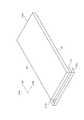
非特許文献1に記載された光学素子について、図15を用いて以下に説明する。図15は、光学素子を用いたディスプレイ装置の構成を模式的に示す構成図である。ディスプレイ装置19´は、映像投影部30´と光学素子10´とを含んで構成される。 The optical element described in
映像投影部30´は、表示素子31´と投影レンズ32´とを含んで構成される。表示素子31´に表示される画像が投影レンズ32´により遠方に投影される。なお、投影レンズ32´の射出瞳に観察者の目を合わせることにより、投影される画像を観察することが可能である。しかし、投影レンズ32´の射出瞳は一つだけなので、表示素子31´に表示される画像を観察可能な視点は1箇所に限定される。 The
光学素子10´は、第1、第2の透明媒体33a´、33b´と体積ホログラムシート34´とによって構成される。第1、第2の透明媒体33a´、33b´は平板状であり、体積ホログラムシート34´は第1、第2の透明媒体33a´、33b´によって挟持される。体積ホログラムシート34´は、入射する光を直進光と回折光とに分岐する。なお、図15において、第1、第2の透明媒体33a´、33b´の長さ方向をx方向、幅方向をy方向とする。 The
光学素子10´の第1の透明媒体33a´側の表面には三角プリズム35´が密着される。映像投影部30´から投影される光束Lxが三角プリズム35´を介して光学素子10´に斜方から入射するよう、且つ後述する条件を満たすように、映像投影部30´は配置される。 A triangular prism 35 'is in close contact with the surface of the optical element 10' on the first
光学素子10´に斜方から入射した光束Lxは、第1、第2の透明媒体33a´、33b´側の表面である第1、第2の表面36a´、36b´間を反射しながら、x方向に伝播される。なお、光束Lxが第1、第2の表面36´a、36b´において全反射するように、映像投影部30´は配置される。 The light beam Lx incident obliquely on the
前述のように、体積ホログラムシート34´に入射する光束Lxは、直進光と回折光に分岐される。例えば、第1の表面36a´側から体積ホログラムシート34´に入射する光は、第2の表面36b´に垂直な方向に回折された回折光と第2の透明媒体33b´に斜方に入射する直進光とに分岐される。 As described above, the light beam Lx incident on the
回折光は第2の表面36b´において透過され、外部に射出される。直進光は第2の表面36b´において全反射され、体積ホログラムシート34´を介して第1の透明媒体33a´に入射する。以後同様に、第1、第2の表面36a´、36b´における全反射、および体積ホログラムシート34´における分岐が繰返され、画像を形成する光束Lxが第2の表面36b´の複数の位置から射出される。言い換えると、複数の射出瞳のコピーが第2の表面側に生成される。 The diffracted light is transmitted through the
複数の射出瞳のコピーが生成されることにより、複数の視点epにおいて画像を観察可能となる。なお、投影レンズ32´の射出瞳の径と複数のコピーの形成位置の間隔とを一致させることにより、射出瞳のコピー同士が接して一体となり、第2の表面36´の面内であればどの視点からでも画像を観察可能となる。したがって、光学素子10´により射出瞳が拡大されたとみなすことが可能である。 By generating a plurality of copies of the exit pupil, an image can be observed at a plurality of viewpoints ep. Note that by matching the diameter of the exit pupil of the
しかし、第2の透明媒体33b´から体積ホログラムシート34´に光束Lxが入射するときにも、光束Lxは回折光と直進光とに分岐される。したがって、複数の射出瞳のコピーは第1の表面36a´側にも生成される。光学素子10´は一方の面からの観察が可能な構成であればよく、両面に光束Lxが射出されることにより光の利用効率が低下していた。 However, even when the light beam Lx enters the
従って、上記のような問題点に鑑みてなされた本発明では、光の利用効率を改善させ得る光学素子の提供を目的とする。 Therefore, an object of the present invention made in view of the above problems is to provide an optical element capable of improving the light utilization efficiency.
上述した諸課題を解決すべく、本発明による光学素子は、
対向する第1、第2の平面を有する板状に形成され、第1、第2の平面の間で所定の角度で入射する光を反射させながら伝播させる第1の導波部と、
第1の導波部の第1の平面に密着され、導波部から入射する光を透過光と反射光とに分離する第1のビームスプリット膜と、
第1のビームスプリット膜を介して第1の導波部に接合され、所定の角度で第1の平面に入射し第1のビームスプリット膜を透過した光を第1のビームスプリット膜の面に実質的に垂直な方向に反射する複数の第1の反射面が第1の方向に沿って並べられる第1の偏向部とを備え、
第1のビームスプリット膜は、第1の導波部から所定の角度で入射する光の大部分を反射し、第1の偏向部から実質的に垂直に入射する光の大部分またはすべてを透過する
ことを特徴とするものである。In order to solve the above-described problems, the optical element according to the present invention is
A first waveguide section that is formed in a plate shape having first and second planes facing each other and that propagates light incident at a predetermined angle between the first and second planes;
A first beam splitting film that is in close contact with the first plane of the first waveguide section and separates light incident from the waveguide section into transmitted light and reflected light;
Light that is joined to the first waveguide through the first beam split film, is incident on the first plane at a predetermined angle, and passes through the first beam split film is incident on the surface of the first beam split film. A plurality of first reflecting surfaces that reflect in a substantially vertical direction are arranged along the first direction;
The first beam splitting film reflects most of the light incident from the first waveguide unit at a predetermined angle, and transmits most or all of the light incident substantially perpendicularly from the first deflecting unit. It is characterized by doing.
上述した諸課題を解決すべく、本発明による光学機構は、
対向する第1、第2の平面を有する板状に形成され第1、第2の平面の間で所定の角度で入射する光を反射させながら伝播させる第1の導波部と、第1の導波部の第1の平面に密着され導波部から入射する光を透過光と反射光とに分離する第1のビームスプリット膜と、第1のビームスプリット膜を介して第1の導波部に接合され所定の角度で第1の平面に入射し第1のビームスプリット膜を透過した光を第1のビームスプリット膜の面に実質的に垂直な方向に反射する複数の第1の反射面が第1の方向に沿って並べられる第1の偏向部とを備え、第1のビームスプリット膜は第1の導波部から所定の角度で入射する光の大部分を反射し第1の偏向部から実質的に垂直に入射する光の大部分またはすべてを透過し、第1の反射面と第1の平面との間の角度が所定の角度の半角の近傍の角度に定められ、第1の導波部において臨界角以上の角度で第2の平面に光が入射するように光学素子に入射する光を第1の導波部に向けて反射する複数の第2の反射面を有する第1の光学素子と、
対向する第3、第4の平面を有する板状に形成され第3、第4の平面の間で所定の角度で入射する光を反射させながら伝播させる第2の導波部と、第2の導波部の第3の平面に密着され導波部から入射する光を透過光と反射光とに分離する第2のビームスプリット膜と、第2のビームスプリット膜を介して第2の導波部に接合され所定の角度で第3の平面に入射し第2のビームスプリット膜を透過した光を第2のビームスプリット膜の面に実質的に垂直な方向に反射する複数の第3の反射面が第1の方向と異なる第2の方向に沿って並べられる第2の偏向部とを有し、第2のビームスプリット膜は第2の導波部から前記所定の角度で入射する光の大部分を反射し第2の偏向部から実質的に垂直に入射する光の大部分またはすべてを透過する第2の光学素子とを備え、
第2の光学素子の第4の平面から出射する光が複数の第2の反射面に入射するように、第1の光学素子と第2の光学素子とが配置される
ことを特徴とするものである。In order to solve the above-mentioned problems, the optical mechanism according to the present invention is:
A first waveguide section that is formed in a plate shape having first and second planes facing each other and that propagates light that is incident at a predetermined angle between the first and second planes; A first beam split film that is in close contact with the first plane of the waveguide section and separates light incident from the waveguide section into transmitted light and reflected light, and the first waveguide through the first beam split film. A plurality of first reflections that reflect light incident on the first plane at a predetermined angle and transmitted through the first beam splitting film in a direction substantially perpendicular to the surface of the first beam splitting film. A first deflecting unit whose surface is arranged along a first direction, and the first beam splitting film reflects most of light incident at a predetermined angle from the first waveguide unit and The first reflecting surface and the first plane are transmitted through most or all of light incident substantially perpendicularly from the deflecting unit. Is set to an angle in the vicinity of a half angle of the predetermined angle, and the light incident on the optical element is incident on the second plane so that the light is incident on the second plane at an angle greater than the critical angle in the first waveguide section. A first optical element having a plurality of second reflecting surfaces that reflect toward one waveguide section;
A second waveguide section that is formed in a plate shape having third and fourth planes facing each other and that propagates light incident at a predetermined angle between the third and fourth planes; A second beam split film that is in close contact with the third plane of the waveguide section and separates light incident from the waveguide section into transmitted light and reflected light, and a second waveguide through the second beam split film. A plurality of third reflections that reflect light incident on the third plane at a predetermined angle and transmitted through the second beam splitting film in a direction substantially perpendicular to the surface of the second beam splitting film. A second deflecting unit whose surface is arranged along a second direction different from the first direction, and the second beam splitting film is configured to transmit the light incident from the second waveguide unit at the predetermined angle. A second one that reflects most and transmits most or all of the light incident substantially perpendicularly from the second deflector. And an optical element,
The first optical element and the second optical element are arranged such that light emitted from the fourth plane of the second optical element enters the plurality of second reflecting surfaces. It is.
上記のように構成された本発明に係る光学素子によれば、射出瞳を拡大させながら、第1の反射面側からの光の射出を抑制させることが可能である。 According to the optical element according to the present invention configured as described above, it is possible to suppress the emission of light from the first reflecting surface side while enlarging the exit pupil.
以下、本発明の実施形態について、図面を参照して説明する。 Hereinafter, embodiments of the present invention will be described with reference to the drawings.
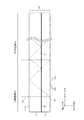
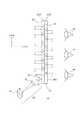
図1は、本発明の第1の実施形態に係る光学素子の斜視図である。 FIG. 1 is a perspective view of an optical element according to the first embodiment of the present invention.
図1に示すように、光学素子10は、導波部11、偏光ビームスプリット膜12、および偏向部13を含んで構成される。導波部11は板状であり、導波部11の片面には偏光ビームスプリット膜12が蒸着により形成される。偏向部13は、平面と、裏側において三角プリズムアレイ(図1において図示せず)が形成された三角プリズムアレイ面とを板面とする板状である。導波部11の偏光ビームスプリット膜12が形成された面(第1の平面)(以後、膜形成面msと呼ぶ)と、偏向部13の平面とを透明接着剤(図示せず)により接合させることにより、光学素子10は形成される。 As shown in FIG. 1, the
なお、光学素子10は全体的に長辺と短辺とを有する長方形の平板状であり、平板の厚さ方向dtに垂直な平面上において長辺に沿った方向を長さ方向dl、厚さ方向dtおよび長辺方向dlに垂直な方向を幅方向dwとする。 The
偏光ビームスプリット膜12は、実質的に垂直な方向から入射する光(第1の光)を透過し、斜方から入射する光の大部分を反射し、残りを透過するようにコンピュータシュミュレーションにより設計され、蒸着される。例えば、S偏光に対して、このような光学特性を有する偏光ビームスプリット膜12が形成可能である。 The polarization
導波部11は、例えば2mmの厚みを有する石英(透明媒質)が用いられる。導波部11に石英を用いることにより、偏光ビームスプリット膜12を蒸着させるときの加熱に対して耐熱性を有し、硬質であるため膜応力に対して反りにくくなる利点を有する。また、硬質であるため、膜形成面msの裏側で全反射面として用いられる面(第2の平面)(以後、入出力ポート面i/osと呼ぶ)に傷つきにくい利点を有する。 For the
偏向部13は、例えば3mmの厚さを有するアクリルが用いられる。偏向部13に形成される三角プリズムアレイは微細であり、射出成型により形成される。それゆえ、射出成型可能な透明媒体としてアクリルが例として選択される。三角プリズムアレイ面psにはアルミ(反射部材)が蒸着される。それゆえ、入射する光は三角プリズムアレイ面psにおいて反射する。 The deflecting
なお、入出力ポート面i/osの長さ方向dlに沿った端部領域が入射領域iaに定められる。一方、入射領域ia以外の領域は射出領域eaに定められる。入射領域iaを含む端部から所定の領域下において偏光ビームスプリット膜12は設けられず、固化した透明接着剤14が介在する。したがって、透明接着剤14が介在した領域において、光束は導波部11と偏向部13との間を透過する。 An end region along the length direction dl of the input / output port surface i / os is defined as the incident region ia. On the other hand, the area other than the incident area ia is defined as the emission area ea. The polarized
図2に示すように、光束Lxは入射領域iaにおいて入出力ポート面i/osに垂直に入射する。垂直に入射した光束Lxは導波部11から偏向部13に入射し、三角プリズムアレイ面psにより斜方に反射される。なお、反射方向にも偏光ビームスプリット膜12は設けられず、斜方に反射された光束Lxは偏向部13から導波部11に斜方から入射する。 As shown in FIG. 2, the light beam Lx enters the input / output port surface i / os perpendicularly in the incident region ia. The vertically incident light beam Lx enters the deflecting
斜方から入射した光束Lxは入出力ポート面i/osで全反射され、偏光ビームスプリット膜12に向きを変えて、その界面において大部分が反射される。なお、後述するように、偏光ビームスプリット膜12において光束Lxの一部は透過する。以後、入出力ポート面i/osでの全反射と偏光ビームスプリット膜12との界面における反射を繰返しながら、光束Lxは長さ方向dlに伝播される。 The light beam Lx incident from an oblique direction is totally reflected at the input / output port surface i / os, changes its direction to the polarization
導波部11の屈折率が偏向部13の屈折率より高いと、偏向部13から導波部11に光束Lxが入射するときに出射角が狭くなる。出射角が狭くなると、長さ方向dlへの単位伝播距離に対する反射回数が増加する。反射回数が増加するため、入射領域iaから反対側の端部までの伝播が困難となる。それゆえ、導波部11の屈折率は偏向部13の屈折率より小さいことが好ましい。なお、石英の屈折率は1.45であり、アクリルの屈折率は1.49であって、導波部11の屈折率は偏向部13の屈折率より小さい。 If the refractive index of the
また、上述のような性質の偏光ビームスプリット膜12は、偏光ビームスプリット膜12の両側の媒体の屈折率が近いほど、上述のような性質を有するような偏光ビームスプリット膜12の設計が容易となる。上述のように、石英とアクリルとの屈折率は比較的近く、上述のような特性の偏光ビームスプリット膜12の設計は容易である。 In addition, the polarizing
三角プリズムアレイ面psには、幅方向dwに延びる複数の第1、第2の三角プリズム15a、15bが形成される。入射領域ia下には、第1の三角プリズム15aが形成され、射出領域ea下には、第2の三角プリズム15bが形成される。第1、第2の三角プリズム15a、15bは、厚さ方向dtに垂直な平面を幅方向dwに平行な直線を軸に傾斜させた傾斜面と、長さ方向dlに垂直な垂直面とを有している。 A plurality of first and second
傾斜面の傾斜角は、第1の三角プリズム15aと第2の三角プリズム15bとで反対向きで、角度の絶対値は等しい。第1の三角プリズム15aの傾斜面(第2の反射面)の法線は導波部11の射出領域ea側に延びる。したがって、前述のように、入出力ポート面i/osから入射領域iaに垂直に入射する光束Lxは、第1の三角プリズム15aにより射出領域eaに向けて反射される。一方、第2の三角プリズム15bの傾斜面(第1の反射面)の法線は導波部11の入射領域ia側に延びる。したがって、後に詳細に説明するように、偏光ビームスプリット膜12を斜方から透過した光束Lxは、入出力ポート面i/osに向かって垂直に反射される。 The inclination angles of the inclined surfaces are opposite in the first
傾斜面の角度は、導波部11の入出力ポート面i/osにおける臨界角に基づいて定められる。導波部11内では、斜方から入射した光束Lxを、入出力ポート面i/osにおける全反射と偏光ビームスプリット膜12における反射とを繰返しながら長さ方向dlに伝播させることが、本実施形態の効果を得るために求められる。それゆえ、入出力ポート面i/osにおいて全反射するように、光束Lxを導波部11に入射させる必要がある。 The angle of the inclined surface is determined based on the critical angle at the input / output port surface i / os of the
入出力ポート面i/osに対する入射角θ(所定の角度)は、臨界角より大きい必要があるので、θ>sin−1(1/n)を満たす必要がある。前述のように、本実施形態における導波部11の材質である石英の屈折率は1.45であるから、θ>sin−1(1/1.45)=43.6°を満たす必要がある。Since the incident angle θ (predetermined angle) with respect to the input / output port surface i / os needs to be larger than the critical angle, it is necessary to satisfy θ> sin−1 (1 / n). As described above, since the refractive index of quartz, which is the material of the
入射角θは第1の三角プリズム15aの傾斜面の角度の倍角なので、傾斜面の角度は入射角θの半角21.8°(=43.6°/2)以上であることが必要である。なお、導波部11と偏向部13との材質は異なっているが、前述のように、偏向部13の屈折率が導波部11の屈折率より大きいので、偏向部13において傾斜面の角度を21.8°以上となるように形成すれば入出力ポート面i/osにおいて光束Lxを全反射させることは可能である。 Since the incident angle θ is a multiple of the angle of the inclined surface of the first
一方、傾斜面の傾斜角が大きくなるほど、隣接する第1の三角プリズム15aの垂直面によってケラレによる光束Lxの光量ロスが増加する。それゆえ、傾斜面の傾斜角は下限値に近くすることが好ましい。それゆえ、本実施形態においては、傾斜面の傾斜角は、例えば25°に定められる。 On the other hand, as the inclination angle of the inclined surface increases, the light amount loss of the light beam Lx due to vignetting increases due to the vertical surface of the adjacent first
なお、傾斜面の傾斜角を25°に定めた場合、入射領域iaにおいて入出力ポート面i/osに垂直に入射する光束Lxは傾斜面により反射され、射出領域eaにおける入出力ポート面i/osに51.6°の入射角で入射する。したがって、入出力ポート面i/osにおける入射角は臨界角より大きいので、光束Lxを入出力ポート面i/osで全反射可能である。この角度を中心として、入出力ポート面i/osへの斜入射光の入射角の振れは、臨界角を下回らない範囲であれば許容されるので、−8°の振れは許容される。 When the inclination angle of the inclined surface is set to 25 °, the light beam Lx incident perpendicularly to the input / output port surface i / os in the incident region ia is reflected by the inclined surface, and the input / output port surface i / in the emission region ea. It is incident on os at an incident angle of 51.6 °. Accordingly, since the incident angle at the input / output port surface i / os is larger than the critical angle, the light beam Lx can be totally reflected at the input / output port surface i / os. With this angle as the center, the fluctuation of the incident angle of the obliquely incident light to the input / output port surface i / os is allowed as long as it does not fall below the critical angle.
複数の第1、第2の三角プリズム15a、15bは、長さ方向dlに沿って並べられる。したがって、幅方向dwから見て、第1、第2の三角プリズム15a、15bは鋸歯状に並ぶ。なお、例えば、第1、第2の三角プリズム15a、15bのピッチは0.9mmである。 The plurality of first and second
第1、第2の三角プリズム15a、15bのピッチが大きくなる程、隣接する第1、第2の三角プリズム15a、15bの垂直面によってケラレによる光束Lxの光量ロスが増加する。一方、ピッチが過剰に小さくなると、回折の影響により反射光が正規反射しなくなるので、0.3mm以上であることが望ましい。本実施形態において、入射光束Lxの幅は5〜10mmであることが仮定されている。したがって、上述の0.9mmのピッチは妥当である。 As the pitch of the first and second
偏光ビームスプリット膜12は、前述のように、実質的に垂直な方向から入射する光を透過し、斜方から入射する光の大部分を反射し、残りを透過するように設計される。例えば、斜入射光に対して反射率95%、透過率5%となるように設計される。また、例えば、略垂直な入射光に対して実質的に100%の透過率となるように設計される。なお、実質的に垂直とは、例えば垂直方向から5°以下の角度とみなすことが出来る。5°以下では、P偏光とS偏光との差が明確に生じない。入射角が5°以下であれば、偏光ビームスプリット膜12の反射率および透過率は、入射角が0°の場合の反射率および透過率と実質的に同じである。 As described above, the polarization
なお、上述の考察により、光学素子10において入出力される光束Lxの画角の許容範囲は7°〜8°と定めることが出来る。 From the above consideration, the allowable range of the angle of view of the light beam Lx input / output in the
上述のような構成の光学素子10の入出力ポート面i/osの入射領域iaに垂直に入射した光束Lxは、第1の三角プリズム15aに反射され、導波部11の射出領域eaに斜方から入射する。斜方から入射した光束Lxは入出力ポート面i/osに臨界角を超える角度で入射し、全反射される。全反射された光束Lxは偏光ビームスプリット膜12に斜方から入射し、95%は反射され、5%は透過する。偏光ビームスプリット膜12に反射された光束Lxは、再び入出力ポート面i/osに臨界角を超える角度で入射し、全反射される。 The light beam Lx incident perpendicularly to the incident area ia of the input / output port surface i / os of the
以後、偏光ビームスプリット膜12における一部反射と、入出力ポート面i/osにおける全反射とを繰返しながら、光束Lxは導波部11の長さ方向dlに伝播される。ただし、偏光ビームスプリット膜12における反射時に5%の光束Lxが透過し、偏向部13に出射する。 Thereafter, the light beam Lx is propagated in the length direction dl of the
偏向部13に出射される光束Lxの出射角は、第1の三角プリズム15aによって反射された光束Lxの導波部11との界面における入射角に等しい。それゆえ、偏向部13に出射された光束Lxは第2の三角プリズム15bによって入出力ポート面i/osに垂直な方向に反射される。垂直な方向に反射された光束Lxは偏光ビームスプリット膜12を実質的に100%の透過率で透過し、入出力ポート面i/osから射出される。 The emission angle of the light beam Lx emitted to the deflecting
導波部11の長さ方向dlの長さは、例えば100mmであり、入射領域iaから射出領域eaに斜入射した光束Lxは、射出領域eaの端部に達するまでに入出力ポート面i/osと偏光ビームスプリット膜12との間を約20回反射する。反射のたびに偏光ビームスプリット膜12において光路が分岐され、前述のように、入出力ポート面i/osから射出される。したがって、100mmの長さに対して約20本の分岐光がアレイを形成する。したがって、分岐光を入出力ポート面i/osから隙間無く射出させるには、5mm(100mm/20)以上の径の光束Lxを入射する必要がある。 The length of the
前述のように、導波部11に伝播される光束Lxは、偏光ビームスプリット膜12で反射を繰返す度に、一部の光量を分岐光として射出されるので、射出光の強度は反射回数に応じて等比級数的に減少する(図3参照)。したがって、偏光ビームスプリット膜12の斜入射光に対する透過率を高くすると、導波部11の末端まで入射光束Lxを伝播させることが難しくなる。 As described above, the light beam Lx propagated to the
本実施形態においては、偏光ビームスプリット膜12の斜入射光に対して設定すべき透過率を簡易的に100%/(反射回数)と定め、上述の反射回数を用いて透過率は5%に定められる。また、反射率は100%−(透過率%)を算出することにより95%に定められる。 In this embodiment, the transmittance to be set for the obliquely incident light of the polarizing
なお、上述のように定めた透過率および反射率を用いると、入出力ポート面i/osから最初に射出される光束Lxと、最後に射出される光束Lxとの強度比は2.5倍程度となり、明るさにムラが生じることが分かる。明るさのムラを低減化させるには、透過率をより小さく設定すればよい。例えば、透過率を3%、反射率を97%とする設定では、入出力ポート面i/osから最初に射出される光束Lxと、最後に射出される光束Lxとの強度比は1.8倍程度に改善される。 If the transmittance and reflectance determined as described above are used, the intensity ratio between the light beam Lx emitted first from the input / output port surface i / os and the light beam Lx emitted last is 2.5 times. It can be seen that the brightness is uneven. In order to reduce unevenness in brightness, the transmittance may be set smaller. For example, in a setting where the transmittance is 3% and the reflectance is 97%, the intensity ratio between the light beam Lx emitted first from the input / output port surface i / os and the light beam Lx emitted last is 1.8. It is improved about twice.
しかし、透過率を小さく設定すると、射出されずに射出領域eaの端部に到達する光量が増加し、入射光束Lxのエネルギーロスが増加する。すなわち、光の利用効率が低下する。本実施形態における透過率5%および反射率95%の設定では、入出力ポート面i/osから射出される光束Lxの全光量は入射光束Lxの64%である。一方で、比較例として挙げた透過率3%および反射率97%の設定では、入出力ポート面i/osから射出される光束Lxの全光量は入射光束Lxの46%に低下する。 However, if the transmittance is set small, the amount of light that reaches the end of the exit area ea without being emitted increases, and the energy loss of the incident light beam Lx increases. That is, the light use efficiency decreases. In this embodiment, when the transmittance is 5% and the reflectance is 95%, the total amount of the light beam Lx emitted from the input / output port surface i / os is 64% of the incident light beam Lx. On the other hand, in the setting of the transmittance of 3% and the reflectance of 97% given as the comparative example, the total light amount of the light beam Lx emitted from the input / output port surface i / os is reduced to 46% of the incident light beam Lx.
このように、明るさのムラの低減化を図ると、光の利用効率は低下する。そこで、透過率は、明るさのムラと光の利用効率とが最適化されるように定められることが好ましい。ところで、視覚は対数感度であるため、後述するディスプレイ装置(図1〜図3において図示せず)に光学素子10を用いる場合には、2.5倍程度の明るさのムラは感知されにくい。また、偏光ビームスプリット膜12の蒸着時の特性のばらつきを考慮すると、透過率を例えば5%より低くなるように形成することは難しい。それゆえ、本実施形態における透過率の設定は、使用目的を満たす十分な低さの明るさムラに抑えながら光の利用効率を高く維持し、実際の形成を可能にさせる設定である。 As described above, when the unevenness of brightness is reduced, the light use efficiency is lowered. Therefore, it is preferable that the transmittance is determined so that the uneven brightness and the light use efficiency are optimized. By the way, since vision is logarithmic sensitivity, when the
上述のように、偏光ビームスプリット膜12は、S偏光の斜入射光においては反射率95%および透過率5%の特性を有し、略垂直入射光においては実質的に100%の透過率の特性を有する。この相反する特性を、ローパス型またはバンドパス型の分光反射特性を有する薄膜は有し得る。 As described above, the polarization
従来知られているように、薄膜において入射角に応じて分光曲線が波長方向にシフトする。図4に示すように、略垂直入射光に対する分光曲線(破線参照)は、斜入射光に対する分光曲線(実線参照)から、長波長側にシフトする。斜入射光に対する分光曲線と、略垂直入射光に対する分光曲線との両者のカットオフ波長に挟まれ、斜入射光に対して反射率が95%、略垂直入射光に対して反射率が0%となるように、入射光束Lxの波長および薄膜の設定を組合わせることにより、本実施形態の偏光ビームスプリット膜12を形成可能となる。 As is conventionally known, the spectral curve shifts in the wavelength direction according to the incident angle in the thin film. As shown in FIG. 4, the spectral curve (see the broken line) for the substantially perpendicular incident light is shifted to the long wavelength side from the spectral curve (see the solid line) for the oblique incident light. It is sandwiched between the cut-off wavelengths of the spectral curve for obliquely incident light and the spectral curve for substantially perpendicularly incident light. The reflectance is 95% for obliquely incident light and 0% for substantially perpendicularly incident light. Thus, by combining the wavelength of the incident light beam Lx and the setting of the thin film, the polarization
なお、分光曲線のシフト量Δλは、Δλ=(1−cosθ´)×λ0により算出される。なお、θ´は薄膜に進入するときの屈折角、λ0は入射光の波長である。本実施形態における偏光ビームスプリット膜12に入射する光束Lxの屈折角は51.6°である。したがって、λ0=635nmの波長の単色光を入射すれば、Δλ=240nmの大きなシフト量を得ることが可能である。したがって、λ=635nmの波長のS偏光の光束Lxに対して、斜入射光の大部分を反射し、略垂直入射光の殆どを透過する偏光ビームスプリット膜12を実際に形成可能である。The shift amount Δλ of the spectral curve is calculated by Δλ = (1−cos θ ′) × λ0 . Θ ′ is the refraction angle when entering the thin film, and λ0 is the wavelength of the incident light. In this embodiment, the refraction angle of the light beam Lx incident on the polarization
上述のような構成の光学素子10では、100mm当たり約20本の光束Lxが射出されるので、入出力ポート面i/osの入射領域iaに、幅が5mm以上の光束Lxを入射すると、隣接する射出光束Lxが互いに接し、全体で幅が100mmの光束となって射出される。すなわち、光束の幅が5mmから100mmに拡大されるので、従来技術と同様に、光学素子10は瞳拡大光学素子として機能する。 In the
以上のような構成の第1の実施形態の光学素子10によれば、入射した光束Lxを平板状の一方の板面である入出力ポート面i/osのみから拡大して射出するので、瞳を拡大させる機能を有しながら、両面から光束を拡大して射出する従来の体積ホログラムシートを用いた光学素子に比べて、光の利用効率を改善させることが可能である。光の利用効率が改善されるので、従来に比べて光源(図1〜図4に図示せず)からの出射光量を低減化可能であり、電力の消費量を低減化させることが可能である。 According to the
次に、第1の実施形態の光学素子10を用いた、2次元状に瞳を拡大させる第1の実施形態の光学機構について説明する。図5に示すように、光学機構16は、第1、第2の瞳拡大板17a、17bとλ/2波長板18とによって構成される。第1の瞳拡大板17aは、サイズと偏光ビームスプリット膜12の設定とを後述するように変更した上述の光学素子10である。また、第2の瞳拡大板17bは、上述の光学素子11と同一である。 Next, the optical mechanism of the first embodiment that uses the
第1の瞳拡大板17aは、幅(幅方向dwの長さ)が10mm、射出領域ea(図5に図示せず)の長さ(長さ方向dlの長さ)が50mmになるように形成される。第2の瞳拡大板17bは、幅(幅方向dwの長さ)が50mm、入射領域ia(図5に図示せず)および射出領域eaそれぞれの長さ(長さ方向dlの長さ)が10mmおよび100mmになるように形成される。 The first
第1、第2の瞳拡大板17a、17bによって、λ/2波長板18が挟まれる。また、第1の瞳拡大板17aの長辺(長さ方向の辺)と第2の瞳拡大板17bの短辺(幅方向の辺)とが重なるように、第1の瞳拡大板17aの入出力ポート面i/osの射出領域eaと第2の瞳拡大板17bの入出力ポート面i/osの入射領域iaが対向するように、且つ第1の瞳拡大板17aの入射領域iaが第2の瞳拡大板17bから突出するように、第1、第2の瞳拡大板17a、17bは重ねられる。 The λ / 2
なお、図5において、第1の瞳拡大板17aの長さ方向および第2の瞳拡大板17bの幅方向に平行な方向をx方向、第1の瞳拡大板17aの幅方向および第2の瞳拡大板17bの長さ方向に平行な方向をy方向、および第1、第2の瞳拡大板17a、17bの厚さ方向に平行な方向をz方向とする In FIG. 5, the direction parallel to the length direction of the first
第1の瞳拡大板17aとλ/2波長板18との間には、空隙が設けられる。第1の瞳拡大板17aにおいて、全反射をさせる射出領域eaの入出力ポート面i/osがλ/2波長板18に対向している。それゆえ、入出力ポート面i/osとλ/2波長板18とを接合させると、第1の瞳拡大板17a内で入出力ポート面i/osにおいて全反射せずに透過することが生じ得る。それゆえ、空隙を設けることにより、第1の瞳拡大板17a内を伝播する光の入出力ポート面i/osにおける全反射が保障される。 A gap is provided between the first
第1の瞳拡大板17aの偏光ビームスプリット膜12は、斜入射光の反射率および透過率がそれぞれ90%および10%となるように設計され、形成される。第1の瞳拡大板17aによる入射光束の伝播方向の長さは50mmであって、上述の光学素子10の長さ(100mm)の半分である。それゆえ、第1の瞳拡大板17aの射出領域eaの端部に到達するまでの偏光ビームスプリット膜12における反射回数は光学素子10における反射回数の約半分となる。それゆえ、第1の瞳拡大板17aの偏光ビームスプリット膜12の透過率を光学素子10の倍にすることによって、明るさのムラと光の利用効率とが最適化される。 The polarization
上述の光学機構16の第1の瞳拡大板17aの入射領域iaに光束Lxを垂直に入射させると、光束Lxはx方向に瞳が拡大されて、第1の瞳拡大板17aの射出領域eaから射出される。 When the light beam Lx is vertically incident on the incident area ia of the first
第1の瞳拡大板17aから射出された光束は、λ/2波長板18によって光束Lxの偏光面を90°回転させる。偏光面を90°回転させることにより、第2の瞳拡大板17bの偏光ビームスプリット膜12にS偏光で光束Lxを入射させることが可能となる。 The light beam emitted from the first
偏光面を回転させた光束は、第2の瞳拡大板17bの入射領域iaに垂直に入射する。第2の瞳拡大板17bに入射した光束はy方向に瞳が拡大されて、第2の瞳拡大板17bの射出領域eaから射出される。 The light beam whose polarization plane has been rotated is perpendicularly incident on the incident area ia of the second
したがって、例えば第1の瞳拡大板17aの入射領域iaに入射した5×5mmの光束を入射させると、第2の瞳拡大板17bの射出領域eaから、瞳がx方向に50mm、y方向に100mmに拡大された投射光が射出される。 Therefore, for example, when a 5 × 5 mm light beam incident on the incident area ia of the first
次に、上述の光学機構16を用いたディスプレイ装置について図6、図7を用いて説明する。図6はディスプレイ装置における各部位の光学配置を示す斜視図である。図7はディスプレイ装置における各部位の光学配置を示す平面図である。 Next, a display device using the
ディスプレイ装置19は、光源20、透過型チャート21、および光学機構16を含んで構成される。光源20から照明光が発せられ、透過型チャート21が照明される。照明による透過型チャート21の投影光が光学機構16に入射する。入射した投影光は、光学機構16により瞳が拡大され射出される。なお、透過型チャート21の代わりに、液晶表示素子を用いて表示する画像を形成し、光学機構16に投影する構成であってもよい。 The
光源20と透過型チャート21との間、および透過型チャート21と光学機構16との間には、それぞれ照明光学系22および投影光学系23が配置される。光源20、照明光学系22、透過型チャート21、投影光学系23、および光学機構16は、光学的に結合される。 An illumination
光源20からは波長635nmのレーザが照明光として出射される。光源20は光源ドライバ24によって駆動される。光源を駆動するための電力は、バッテリ25から供給される。 A laser having a wavelength of 635 nm is emitted from the
照明光は照明光学系22を介して透過型チャート21に照射される。透過型チャート21は、例えば5.6mm×4.5mmの大きさを有している。透過型チャート21の投影光は、投影光学系23により光学機構16の第1の瞳拡大板17aの入射領域iaに投影される。なお、投影光学系23の射出瞳と光学機構16の第1の瞳拡大板17aの入射領域iaとは合わせられている。 The illumination light is applied to the
投影光学系23は、例えば焦点距離が28mmであり、投影光を無限遠方に投影可能である。投影光の投射の画角は、水平方向に±5.7°、垂直方向に±4.6°になる。なお、この画角は、本実施形態の光学機構16に用いられる光学素子10の入射角の許容範囲内である。投影光学系23により、透過型チャート21の投影光は直径10mmの瞳として光学機構16に入射する。 The projection
光学機構16を用いない場合には、投影光学系23の射出瞳に観察者の目を合わせることによりチャートの像を観察可能である。しかし、直径10mmの射出瞳に目を合わせ続けるのは観察者にとって苦痛である。一方、本実施形態におけるディスプレイ装置19では、光学機構16により瞳の大きさが100mm×50mmに拡大されるので、観察者にとって拡大された射出瞳に目を合わせることは容易である。 When the
例えば、図8に示すように、ディスプレイ装置19の光学機構16の射出領域eaから200mm程離れた位置において、画像観察が可能となる。さらには、任意の距離で、横50mm×縦40mmの大きさのチャート像を見ることが出来る。なお、ディスプレイ装置19によって、無限遠方に像が形成されるため、遠視や老視でも投影像を見ることが可能である。 For example, as shown in FIG. 8, the image can be observed at a position about 200 mm away from the emission area ea of the
次に、本発明の第2の実施形態に係る光学素子および光学機構について説明する。第2の実施形態は、光学素子の入出力ポート面が偏光高反射膜とカバーガラスによって覆われる点、および光学機構の構成が第1の実施形態と異なっている。以下に、第1の実施形態と異なる点を中心に第2の実施形態について説明する。なお、第1の実施形態と同じ機能および構成を有する部位には同じ符号を付す。 Next, an optical element and an optical mechanism according to the second embodiment of the present invention will be described. The second embodiment is different from the first embodiment in that the input / output port surface of the optical element is covered with a highly reflective polarizing film and a cover glass, and the configuration of the optical mechanism. The second embodiment will be described below with a focus on differences from the first embodiment. In addition, the same code | symbol is attached | subjected to the site | part which has the same function and structure as 1st Embodiment.
図9に示すように、第2の実施形態の光学素子100は、導波部11、偏光ビームスプリット膜12、偏向部13、偏光高反射膜26(傾斜光反射膜)、およびカバーガラス27(カバー)を含んで構成される。導波部11、偏光ビームスプリット膜12、および偏向部13の構成および機能は、第1の実施形態と同じである。 As shown in FIG. 9, the
導波部11の入出力ポート面i/osの全面に、偏光高反射膜26が蒸着される。偏光高反射膜26は、実質的に垂直な方向から入射する光を透過し、斜方から入射する光を実質的に100%の反射率で反射するようにコンピュータシュミュレーションにより設計される。偏光高反射膜26の全面がさらにカバーガラス27によって覆われる。 A polarization highly
第1の実施形態と同様に、入出力ポート面i/os側の入射領域iaに垂直に入射した光束Lxは、第1の三角プリズム15aに反射され、導波部11の射出領域eaに斜方から入射する。第1の実施携帯と異なり、斜方から入射した光束Lxは斜方から偏光高反射膜26に入射し、反射される。 Similar to the first embodiment, the light beam Lx perpendicularly incident on the incident area ia on the input / output port surface i / os side is reflected by the first
以後、第1の実施形態と同様に、偏光ビームスプリット膜12での部分的な透過および大部分の反射と偏光高反射膜26における反射を繰返しながら、光束Lxは長さ方向dlに伝播される。 Thereafter, as in the first embodiment, the light beam Lx is propagated in the length direction dl while repeating partial transmission and most reflection on the polarization
偏光ビームスプリット膜12を透過した光束Lxは第2の三角プリズム15bによって、入出力ポート面i/osに垂直な方向に反射される。したがって、反射された光束Lxは偏光ビームスプリット膜12、偏光高反射膜26、およびカバーガラス27を透過して入出力ポート面i/osから射出される。 The light beam Lx that has passed through the polarization
したがって、第2の実施形態の光学素子100は、第1の実施形態の光学素子10と同様に、入射領域iaに入射する光束の瞳を拡大する機能を有する。 Therefore, the
以上のような構成の第2の実施形態の光学素子によっても、入射した光束を平板状の一方の板面のみから拡大して射出するので、瞳を拡大させる機能を有しながら、光の利用効率を改善させることが可能である。 Even with the optical element of the second embodiment configured as described above, the incident light beam is enlarged and emitted only from one flat plate surface, so that the use of light is possible while having the function of enlarging the pupil. Efficiency can be improved.
また、第2の実施形態の光学素子100によれば、カバーガラス27で表面が覆われているので、反射機能を低減させる、偏光高反射膜26および入出力ポート面i/osの損傷や汚れの付着が防止される。したがって、光束の伝播機能を維持することが可能である。 Further, according to the
次に、第2の実施形態の光学素子100を用いた、2次元状に瞳を拡大させる第2の実施形態の光学機構について説明する。第2の実施形態の光学機構は、第1の実施形態の光学機構と同じく、第1、第2の瞳拡大板17a、17b(第1、第2の光学素子)とλ/2波長板18とによって構成される。第1の実施形態と異なり、第1、第2の瞳拡大板17a、17bは、第2の実施形態の光学素子100である。 Next, an optical mechanism according to the second embodiment that uses the
第2の実施形態では、第1の実施形態と異なり、第1の瞳拡大板17aとλ/2波長板18との間に空隙は設けられず、密着して固定される。第2の実施形態の光学素子100はカバーガラス27の内側の界面において光束が反射するので、空隙を設けなくても斜入射光が透過することはない。それゆえ、第1の瞳拡大板17aとλ/2波長板18とを密着させることにより、機械的強度を向上させることが可能である。 In the second embodiment, unlike the first embodiment, no gap is provided between the first
次に、本発明の第3の実施形態に係る光学素子および光学機構について説明する。第3の実施形態は、入射領域iaにおける三角プリズムアレイが形成される部位が第1の実施形態と異なっている。以下に、第1の実施形態と異なる点を中心に第3の実施形態について説明する。なお、第1の実施形態と同じ機能および構成を有する部位には同じ符号を付す。 Next, an optical element and an optical mechanism according to a third embodiment of the present invention will be described. The third embodiment is different from the first embodiment in the part where the triangular prism array is formed in the incident area ia. The third embodiment will be described below with a focus on differences from the first embodiment. In addition, the same code | symbol is attached | subjected to the site | part which has the same function and structure as 1st Embodiment.
図10に示すように、第3の実施形態の光学素子101は、導波部111、偏光ビームスプリット膜12、および偏向部131を含んで構成される。第1の実施形態と同じく、射出領域ea下における偏向部131の三角プリズムアレイ面psには複数の第2の三角プリズム15bが形成される。第2の三角プリズム15bの形状は、第1の実施形態と同じである。また、第1の実施形態と同じく、導波部111の入出力ポート面i/osの射出領域eaは平面状である。 As shown in FIG. 10, the
一方、第1の実施形態と異なり、入射領域ia下における三角プリズムアレイ面psは、平面状である。また、第1の実施形態と異なり、入出力ポート面i/osの入射領域iaには、複数の第3の三角プリズム15cが形成される。 On the other hand, unlike the first embodiment, the triangular prism array surface ps under the incident area ia is planar. Further, unlike the first embodiment, a plurality of third
第3の三角プリズム15cの形状は、第1の三角プリズム15aと同様に傾斜面と垂直面とを有する。幅方向dwと長さ方向dlとに平行な平面に対する傾斜面の傾斜角は、第1のプリズム15aと同様に、25°である。 The shape of the third
上述のような構成の光学素子101の入射領域ia下において三角プリズムアレイ面psに垂直に入射した光束Lxは、第3の三角プリズム15cに反射され、偏光ビームスプリット膜12に導かれる。反射された光束Lxは、偏光ビームスプリット膜12に斜方から入射して、95%が反射され、5%が透過される。 The light beam Lx incident perpendicularly to the triangular prism array surface ps under the incident area ia of the
以後、第1の実施形態と同様に、偏光ビームスプリット膜12における一部反射と、入出力ポート面i/osにおける全反射とを繰返しながら、光束Lxは導波部111の長さ方向dlに伝播される。また、第1の実施形態と同じく、偏光ビームスプリット膜12における反射時に5%の光束Lxが透過し、偏向部131に出射する。 Thereafter, as in the first embodiment, the light beam Lx is repeated in the length direction dl of the waveguide 111 while repeating partial reflection at the polarization
以上のような構成の第3の実施形態の光学素子101によっても、入射した光束Lxを平板状の一方の板面のみから拡大して射出するので、瞳を拡大させる機能を有しながら、光の利用効率を改善させることが可能である。 Also with the
次に、第3の実施形態の光学素子101を用いて、2次元状に瞳を拡大させる第3の実施形態の光学機構について説明する。第3の実施形態の光学機構は、第1の実施形態の光学機構と同じく、第1、第2の瞳拡大板171a、171bとλ/2波長板18とによって構成される。第1の実施形態と異なり、第1、第2の瞳拡大板171a、171bは、第3の実施形態の光学素子101である。 Next, an optical mechanism according to the third embodiment that enlarges the pupil two-dimensionally using the
図11に示すように、第1の実施形態と同様に、第1、第2の瞳拡大板171a、171bによって、λ/2波長板18が挟まれる。第1の実施形態と同様に、第1の瞳拡大板171aの長辺と第2の瞳拡大板171bの短辺とが重なるように、且つ第1の瞳拡大板171aの入射領域iaが第2の瞳拡大板171bから突出するように、第1、第2の瞳拡大板171a、171bは重ねられる。第1の実施形態と異なり、第1の瞳拡大板171aの入出力ポート面i/osの射出領域ea(図11において図示せず)と第2の瞳拡大板171bの三角プリズムアレイ面psの入射領域ia(図11において図示せず)とが対向するように、第1、第2の瞳拡大板171a、171bは重ねられる。 As shown in FIG. 11, similarly to the first embodiment, the λ / 2
以上のような構成の第3の実施形態の光学機構161によれば、2次元状に拡大した瞳を射出する面、すなわち、第2の瞳拡大板171bの入出力ポート面i/os側に第1の瞳拡大板171aのような構成部位を配置する必要がなくなる。それゆえ、光学機構161は、以下に説明するように、配置上の効果を有する。 According to the
第3の実施形態の光学機構161を用いたディスプレイ装置について、図12を用いて説明する。ディスプレイ装置191は、本体28と第2の瞳拡大板171bとを含んで構成される。本体28内に、プロジェクタ光学系29と第1の瞳拡大板171aおよびλ/2波長板18とが設けられる。プロジェクタ光学系29は、光源(図示せず)、照明光学系(図示せず)、透過型チャート(図示せず)、および投影光学系(図示せず)を有する。したがって、プロジェクタ光学系29により、チャートの投影光が光学機構161に投影される。 A display device using the
第1の瞳拡大板171aおよびλ/2波長板18は、λ/2波長板18が本体の表面から露出した状態で、本体28に埋設される。本体28には支持機構(図示せず)が設けられる。支持機構は、第2の瞳拡大板171bの三角プリズムアレイ面psと本体28のλ/2波長板18を露出させた面とを平行に保ちながら、第2の瞳拡大板171bを長さ方向に滑動自在に支持する。 The first
支持機構は、第2の瞳拡大板171bの入射領域iaとλ/2波長板18とが重なる位置において、第2の瞳拡大板171bを係止可能である。第2の瞳拡大板171bの入射領域iaとλ/2波長板18とが重ね合わせることにより、第2の瞳拡大板171bの入出力ポート面i/osからチャートの投影像が射出可能となる。 The support mechanism can lock the second
上述のような、表示面を本体から滑動可能なディスプレイ装置において、第1、第2の実施形態の光学機構16を適用すると、表示面(第2の瞳拡大板17bの入出力ポート面i/os)上に第1の瞳拡大板17aとλ/2波長板18とを配置する必要がある。しかし、このようなディスプレイ装置においては、表示面上に他の素子などが設けられることは好ましくない。一方、第3の実施形態の光学機構161によれば、第1の瞳拡大板171aおよびλ/2波長板18が第2の瞳拡大板171bの三角プリズムアレイ面ps側に配置されるので、光学機構161全体として第2の瞳拡大板171b側の表面を平坦化させることが可能である。したがって、第3の実施形態の光学機構161は、上述のようなディスプレイ装置に適している。 In the display device that can slide the display surface from the main body as described above, when the
また、表示面を本体から滑動可能な従来のディスプレイ装置では、表示面に電装部品が設けられ、本体の回路などと接続される。しかし、本実施形態の光学機構161を用いる場合には、第2の瞳拡大板171bに電装部品を設ける必要が無く、第2の瞳拡大板171bと本体28との間に接続用の配線が不要である。配線が不要なので、従来のディスプレイ装置に用いられる表示パネルに比べて、耐久性および耐水性を向上させることが可能である。 Moreover, in the conventional display apparatus which can slide a display surface from a main body, an electrical component is provided in a display surface and it connects with the circuit of a main body. However, when the
次に、本発明の第4の実施形態に係る光学素子について説明する。第4の実施形態は、偏向部の厚さが第1の実施形態と異なっている。以下に、第1の実施形態と異なる点を中心に第4の実施形態について説明する。なお、第1の実施形態と同じ機能および構成を有する部位には同じ符号を付す。 Next, an optical element according to the fourth embodiment of the present invention will be described. The fourth embodiment is different from the first embodiment in the thickness of the deflecting portion. The fourth embodiment will be described below with a focus on differences from the first embodiment. In addition, the same code | symbol is attached | subjected to the site | part which has the same function and structure as 1st Embodiment.
図13に示すように、第4の実施形態の光学素子102は、導波部11、偏光ビームスプリット膜12、および偏向部132を含んで構成される。導波部11および偏光ビームスプリット膜12の構成および機能は、第1の実施形態と同じである。 As shown in FIG. 13, the
偏向部132は、第1の実施形態と異なり、三角プリズムアレイ面psを形成するだけの厚みを有する。すなわち、偏光ビームスプリット膜12上に直接、複数の第1、第2の三角プリズム15a、15bが形成される。例えば、第1の実施形態と同様に導波部11に偏光ビームスプリット膜12を形成し、導波部11の膜形成面に紫外線硬化型の透明樹脂を塗布した後成型型を押し当てた状態で紫外線を照射することにより樹脂を硬化させることにより、入射領域ia下および射出領域ea下それぞれに第1の三角プリズム15aおよび第2の三角プリズム15bが形成される。 Unlike the first embodiment, the deflecting unit 132 has a thickness sufficient to form the triangular prism array surface ps. That is, a plurality of first and second
以上のような構成の第4の実施形態の光学素子によっても、入射した光束を平板状の一方の板面のみから拡大して射出するので、瞳を拡大させる機能を有しながら、光の利用効率を改善させることが可能である。 Even with the optical element of the fourth embodiment configured as described above, the incident light beam is enlarged and emitted only from one flat plate surface, so that the use of light is possible while having the function of enlarging the pupil. Efficiency can be improved.
また、第4の実施形態によれば、光のロスを低減化することが可能である。例えば、第1の実施形態の光学素子10を用いた場合、光束Lxの入射位置が入射領域ia内の射出領域ea寄りである場合に、第1の三角プリズム15aで反射された光束Lxの一部が偏光ビームスプリット膜12に入射することがあり得る。したがって、導波部11に入射する光束の光量が減少し得る。 Further, according to the fourth embodiment, it is possible to reduce light loss. For example, when the
一方、第4の実施形態の光学素子102によれば、偏向部132が薄いため、光束Lxを入射領域ia内の射出領域ea寄りに入射しても、第1の三角プリズム15aにより反射される光束Lxが偏光ビームスプリット膜12に入射する可能性が低い。それゆえ、光のロスを低減化させることが可能となる。 On the other hand, according to the
なお、上述の第4の実施形態特有の構成、すなわち偏向部132の構成は、第2、第3の実施形態の光学素子100、101にも適用可能である。 The configuration unique to the fourth embodiment described above, that is, the configuration of the deflecting unit 132 can be applied to the
次に、本発明の第5の実施形態に係る光学素子について説明する。第5の実施形態は、偏光ビームスプリット膜の構成が第1の実施形態と異なっている。以下に、第1の実施形態と異なる点を中心に第5の実施形態について説明する。なお、第1の実施形態と同じ機能および構成を有する部位には同じ符号を付す。 Next, an optical element according to a fifth embodiment of the present invention will be described. The fifth embodiment is different from the first embodiment in the configuration of the polarization beam splitting film. The fifth embodiment will be described below with a focus on differences from the first embodiment. In addition, the same code | symbol is attached | subjected to the site | part which has the same function and structure as 1st Embodiment.
第5の実施形態の光学素子は、第1の実施形態と同様に、導波部11、偏光ビームスプリット膜12、および偏向部13とを含んで構成される。導波部11および偏向部13の構成および機能は、第1の実施形態と同じである。 As in the first embodiment, the optical element of the fifth embodiment includes a
第1の実施形態と異なり、第5の実施形態では偏光ビームスプリット膜12の斜入射光に対する透過率が一定でなく、長さ方向dlに沿った位置に応じて変えられている。例えば、入射領域ia側の偏光ビームスプリット膜12の一端からの距離に応じて等比級数的に透過率が増加するように(図14参照)、偏光ビームスプリット膜12が形成される。なお、例えば、透過率を段階的に上げるNDフィルタを偏光ビームスプリット膜12に重ねることにより、位置により透過率を変えることが可能である。 Unlike the first embodiment, in the fifth embodiment, the transmittance of the polarization
以上のような構成の第5の実施形態の光学素子によっても、入射した光束を平板状の一方の板面のみから拡大して射出するので、瞳を拡大させる機能を有しながら、光の利用効率を改善させることが可能である。 Even with the optical element of the fifth embodiment configured as described above, the incident light beam is enlarged and emitted only from one flat plate surface, so that the use of light is possible while having the function of enlarging the pupil. Efficiency can be improved.
また、第5の実施形態によれば、明るさのムラを低減化させながら、光の利用効率をさらに改善させることが可能である。上述のように、射出領域ea側において目の位置による明るさのムラと、光の利用効率は相反する関係となる。すなわち、透過率を一様に低減化することにより明るさのムラを減じられる一方で光の利用効率が低下する。一方、透過率を一様に高くすることにより光の利用効率が向上するが明るさのムラが大きくなる。 Further, according to the fifth embodiment, it is possible to further improve the light use efficiency while reducing the unevenness of brightness. As described above, the brightness unevenness due to the position of the eyes on the emission area ea side and the light use efficiency are in a contradictory relationship. That is, by uniformly reducing the transmittance, unevenness in brightness can be reduced, while light utilization efficiency is reduced. On the other hand, by increasing the transmittance uniformly, the light use efficiency is improved, but the brightness unevenness is increased.
これに対して、本実施形態のように、導波部11内で偏光ビームスプリット膜12の入射領域ia側の端部からの距離に応じて透過率を高くする構成であれば、明るさのムラを減らしながら、射出されずに導波部11の端部に到達する光束Lxの光量を減じらせることが可能である。したがって、光の利用効率を向上させることが可能である。 On the other hand, as in the present embodiment, if the transmittance is increased in accordance with the distance from the end of the polarizing
なお、第5の実施形態特有の構成、すなわち偏光ビームスプリット膜12の構成は、第1〜第4の実施形態にも適用可能である。 The configuration peculiar to the fifth embodiment, that is, the configuration of the polarization
次に、本発明の第6の実施形態に係る光学素子について説明する。第6の実施形態は、第1、第2の三角プリズムの構成が第1の実施形態と異なっている。以下に、第1の実施形態と異なる点を中心に第6の実施形態について説明する。なお、第1の実施形態と同じ機能および構成を有する部位には同じ符号を付す。 Next, an optical element according to a sixth embodiment of the present invention will be described. The sixth embodiment is different from the first embodiment in the configuration of the first and second triangular prisms. The sixth embodiment will be described below with a focus on differences from the first embodiment. In addition, the same code | symbol is attached | subjected to the site | part which has the same function and structure as 1st Embodiment.
第6の実施形態の光学素子は、第1の実施形態と同じく、導波部11、偏光ビームスプリット膜12、および偏向部13を含んで構成される。導波部11および偏光ビームスプリット膜12の構成および機能は第1の実施形態と同じである。また、偏向部13の形状そのものは、第1の実施形態と同じである。 As in the first embodiment, the optical element of the sixth embodiment includes a
一方、第1の実施形態と異なり、偏向部13の三角プリズムアレイ面は、アルミでなく、投影光として入射領域iaに入射する光の波長を含む帯域の光を反射し、他の可視光の帯域の光を透過する光学特性を有する反射部材により覆われる。 On the other hand, unlike the first embodiment, the triangular prism array surface of the deflecting
以上のような構成の第6の実施形態の光学素子によっても、入射した光束を平板状の一方の板面のみから拡大して射出するので、瞳を拡大させる機能を有しながら、光の利用効率を改善させることが可能である。 Even with the optical element of the sixth embodiment configured as described above, the incident light beam is enlarged and emitted only from one flat plate surface, so that the use of light is possible while having the function of enlarging the pupil. Efficiency can be improved.
また、第6の実施形態によれば、所定の帯域外の可視光を第1、第2の三角プリズム15a、15bが透過するので、入出力ポート面i/os側から入射光束Lxにより形成される画像と光学素子10の裏側の背景とを観察することが可能である。 Further, according to the sixth embodiment, visible light outside a predetermined band is transmitted by the first and second
なお、第6の実施形態特有の構成、すなわち第1、第2の三角プリズム15a、15bの構成は、第1〜第5の実施形態にも適用可能である。 The configuration unique to the sixth embodiment, that is, the configuration of the first and second
本発明を諸図面や実施例に基づき説明してきたが、当業者であれば本開示に基づき種々の変形や修正を行うことが容易であることに注意されたい。従って、これらの変形や修正は本発明の範囲に含まれることに留意されたい。 Although the present invention has been described based on the drawings and examples, it should be noted that those skilled in the art can easily make various modifications and corrections based on the present disclosure. Therefore, it should be noted that these variations and modifications are included in the scope of the present invention.
例えば、第1〜第6の実施形態において、第1〜第3の三角プリズム15a〜15cのピッチは0.9mmとして例示されているが、0.9mmに限定されない。また、すべてのピッチが等しくなくてもよい。例えば、0.8mm、0.9mm、1.0mmのピッチが混在していても、上述の実施形態の効果を得ることは可能である。 For example, in the first to sixth embodiments, the pitch of the first to third
また、第1〜第6の実施形態において、石英を用いて導波部11、111を形成する構成であるが、他の部材を用いてもよい。例えば、PYLEX(登録商標、コーニング インコーポレーテッド)、TEMPAX Float(登録商標、ショット アクチエンゲゼルシャフト)、バイコール(登録商標、コーニング インコーポレーテッド)などの耐熱ガラスも石英に近い屈折率であり、導波部11、111を形成するのに適している。 In the first to sixth embodiments, the
また、第1〜第6の実施形態において、第1〜第3の三角プリズム15a〜15cの傾斜面の傾斜角は25°として例示されているが、25°に限定されない。入出力ポート面i/osに斜方から入射する光の大部分あるいは実質的に全量が反射され、反射された光が第2の三角プリズム15bによって入出力ポート面i/osに略垂直な方向に反射されれば、どのような角度であってもよい。 In the first to sixth embodiments, the inclination angle of the inclined surfaces of the first to third
また、第1〜第6の実施形態において、光学素子10、100、101に入射する光束Lxは、第1の三角プリズム15aまたは第3の三角プリズム15cによって、導波部11、111に斜方に入射するように反射される構成であるが、他の方法によって導波部11に斜方から入射するように構成してもよい。例えば、図15に示す公知の構成における光学素子10´の外面に設けた三角プリズム35´を用いて斜方から入射させる構成であってもよい。 In the first to sixth embodiments, the light beam Lx incident on the
10、100、101、10´ 光学素子
11、111 導波部
12 偏光ビームスプリット膜
13、131 偏向部
15a、15b、15c 第1、第2、第3の三角プリズム
16 光学機構
17a、171a 第1の瞳拡大板
17b、171b 第2の瞳拡大板
18 λ/2波長板
19、191 ディスプレイ装置
21 透過型チャート
26 偏光高反射膜
27 カバーガラス
30´ 映像投影部
33´a、33´b 第1、第2の透明媒体
34´ 体積ホログラムシート
35´ 三角プリズム
ea 射出領域
ia 入射領域
i/os 入出力ポート面
Lx 光束
ms 膜形成面
ps 三角プリズムアレイ面10, 100, 101, 10 '
Claims (18)
Translated fromJapanese前記第1の導波部の第1の平面に密着され、前記導波部から入射する光を透過光と反射光とに分離する第1のビームスプリット膜と、
前記第1のビームスプリット膜を介して前記第1の導波部に接合され、前記所定の角度で前記第1の平面に入射し前記第1のビームスプリット膜を透過した光を前記第1のビームスプリット膜の面に実質的に垂直な方向に反射する複数の第1の反射面が第1の方向に沿って並べられる第1の偏向部とを備え、
前記第1のビームスプリット膜は、前記第1の導波部から前記所定の角度で入射する光の大部分を反射し、前記第1の偏向部から実質的に垂直に入射する光の大部分またはすべてを透過する
ことを特徴とする光学素子。A first waveguide formed in a plate shape having first and second planes facing each other, and propagating while reflecting light incident at a predetermined angle between the first and second planes;
A first beam splitting film that is in close contact with the first plane of the first waveguide section and separates light incident from the waveguide section into transmitted light and reflected light;
Light that is joined to the first waveguide through the first beam splitting film, is incident on the first plane at the predetermined angle, and passes through the first beam splitting film is transmitted to the first beam splitting film. A plurality of first reflecting surfaces that reflect in a direction substantially perpendicular to the surface of the beam splitting film, and a first deflecting unit arranged along the first direction;
The first beam splitting film reflects most of light incident at the predetermined angle from the first waveguide part, and most of light incident substantially perpendicularly from the first deflection part. Or an optical element characterized by transmitting all.
対向する第3、第4の平面を有する板状に形成され第3、第4の平面の間で前記所定の角度で入射する光を反射させながら伝播させる第2の導波部と、前記第2の導波部の第3の平面に密着され導波部から入射する光を透過光と反射光とに分離する第2のビームスプリット膜と、前記第2のビームスプリット膜を介して前記第2の導波部に接合され前記所定の角度で前記第3の平面に入射し前記第2のビームスプリット膜を透過した光を前記第2のビームスプリット膜の面に実質的に垂直な方向に反射する複数の第3の反射面が前記第1の方向と異なる第2の方向に沿って並べられる第2の偏向部とを有し、第2のビームスプリット膜は前記第2の導波部から前記所定の角度で入射する光の大部分を反射し前記第2の偏向部から実質的に垂直に入射する光の大部分またはすべてを透過する第2の光学素子とを備え、
前記第2の光学素子の前記第4の平面から出射する光が前記複数の第2の反射面に入射するように、前記第1の光学素子と前記第2の光学素子とが配置される
ことを特徴とする光学機構。A first optical element which is the optical element according to claim 9;
A second waveguide formed in a plate shape having third and fourth planes facing each other and propagating while reflecting light incident at the predetermined angle between the third and fourth planes; A second beam split film that is in close contact with the third plane of the second waveguide section and separates light incident from the waveguide section into transmitted light and reflected light, and the second beam split film through the second beam split film. Light that is incident on the third plane at the predetermined angle and transmitted through the second beam splitting film in a direction substantially perpendicular to the surface of the second beam splitting film. A plurality of third reflecting surfaces to be reflected are arranged along a second direction different from the first direction, and the second beam splitting film is the second waveguide unit. Reflecting most of the light incident at the predetermined angle from the second deflecting portion and being substantially perpendicular to the second deflecting portion. And a second optical element that transmits most or all of the incident light,
The first optical element and the second optical element are arranged so that light emitted from the fourth plane of the second optical element enters the plurality of second reflecting surfaces. An optical mechanism characterized by
前記第2の導波部の前記第4の平面に密着され、前記第2の導波部から斜方斜方入射する光を反射し、前記第2の導波部から実質的に垂直な方向に入射する光を透過する傾斜光反射膜を備え、
前記第1の光学素子は、前記傾斜光反射膜に密着するように配置される
ことを特徴とする光学機構。The optical mechanism according to claim 14,
A direction that is in close contact with the fourth plane of the second waveguide, reflects obliquely incident light from the second waveguide, and is substantially perpendicular to the second waveguide. An inclined light reflecting film that transmits light incident on
The first optical element is disposed so as to be in close contact with the inclined light reflecting film.
前記複数の第2の反射面は前記第2の平面と同じ面に形成され、
前記第4の平面が前記第1の光学素子を介して前記複数の第2の反射面に対向するように、前記第1の光学素子と前記第2の光学素子とが配置される
ことを特徴とする光学機構。The optical mechanism according to any one of claims 14 to 16,
The plurality of second reflecting surfaces are formed on the same surface as the second plane,
The first optical element and the second optical element are arranged so that the fourth plane faces the plurality of second reflecting surfaces via the first optical element. An optical mechanism.
前記第1の光学素子は、前記第2の光学素子の前記第4の平面に平行な方向に変位可能に保持され、
前記第1の光学素子が所定の変位位置に変位させた状態において、前記第2の光学素子の前記第4の平面から出射する光が前記複数の第2の反射面に入射する
ことを特徴とする光学機構。The optical mechanism according to any one of claims 14 to 17,
The first optical element is held displaceably in a direction parallel to the fourth plane of the second optical element,
The light emitted from the fourth plane of the second optical element is incident on the plurality of second reflecting surfaces in a state where the first optical element is displaced to a predetermined displacement position. Optical mechanism.
Priority Applications (3)
| Application Number | Priority Date | Filing Date | Title |
|---|---|---|---|
| JP2011199716AJP5901192B2 (en) | 2011-09-13 | 2011-09-13 | Optical mechanism |
| PCT/JP2012/005659WO2013038626A1 (en) | 2011-09-13 | 2012-09-06 | Optical element, and optical mechanism |
| US14/208,409US20140192418A1 (en) | 2011-09-13 | 2014-03-13 | Optical Element and Optical Mechanism |
Applications Claiming Priority (1)
| Application Number | Priority Date | Filing Date | Title |
|---|---|---|---|
| JP2011199716AJP5901192B2 (en) | 2011-09-13 | 2011-09-13 | Optical mechanism |
Publications (3)
| Publication Number | Publication Date |
|---|---|
| JP2013061480Atrue JP2013061480A (en) | 2013-04-04 |
| JP2013061480A5 JP2013061480A5 (en) | 2014-10-16 |
| JP5901192B2 JP5901192B2 (en) | 2016-04-06 |
Family
ID=47882879
Family Applications (1)
| Application Number | Title | Priority Date | Filing Date |
|---|---|---|---|
| JP2011199716AExpired - Fee RelatedJP5901192B2 (en) | 2011-09-13 | 2011-09-13 | Optical mechanism |
Country Status (3)
| Country | Link |
|---|---|
| US (1) | US20140192418A1 (en) |
| JP (1) | JP5901192B2 (en) |
| WO (1) | WO2013038626A1 (en) |
Cited By (32)
| Publication number | Priority date | Publication date | Assignee | Title |
|---|---|---|---|---|
| WO2015111420A1 (en)* | 2014-01-27 | 2015-07-30 | オリンパス株式会社 | Display device |
| WO2015128913A1 (en)* | 2014-02-26 | 2015-09-03 | オリンパス株式会社 | Display apparatus |
| WO2015141168A1 (en)* | 2014-03-20 | 2015-09-24 | オリンパス株式会社 | Image display device |
| JP2015172676A (en)* | 2014-03-12 | 2015-10-01 | オリンパス株式会社 | display device |
| WO2016051439A1 (en)* | 2014-10-03 | 2016-04-07 | オリンパス株式会社 | Display device |
| JP2016535291A (en)* | 2013-09-27 | 2016-11-10 | カール・ツァイス・スマート・オプティクス・ゲゼルシャフト・ミット・ベシュレンクテル・ハフツングCarl Zeiss Smart Optics GmbH | A spectacle lens for a display device that can be worn on the head of a user and generates an image, and a display device including the spectacle lens |
| US9720236B2 (en) | 2014-10-29 | 2017-08-01 | Seiko Epson Corporation | Optical element, electro-optical device, and mounted display apparatus |
| JP2018512608A (en)* | 2015-02-19 | 2018-05-17 | ラマス リミテッド | Compact head-mounted display system that displays uniform images |
| JPWO2017125992A1 (en)* | 2016-01-18 | 2018-05-31 | 株式会社島津製作所 | OPTICAL ELEMENT, DISPLAY DEVICE USING SAME, AND LIGHT RECEIVER |
| JP2020514783A (en)* | 2017-01-26 | 2020-05-21 | ディジレンズ インコーポレイテッド | Waveguide with uniform output illumination |
| WO2020196090A1 (en)* | 2019-03-26 | 2020-10-01 | 東レ株式会社 | Laminated body and manufacturing method thereof, light guide plate unit, light source unit, display device, projection image display member, projection image display device, and display screen filter |
| JPWO2021157044A1 (en)* | 2020-02-07 | 2021-08-12 | ||
| US11256155B2 (en) | 2012-01-06 | 2022-02-22 | Digilens Inc. | Contact image sensor using switchable Bragg gratings |
| US11281013B2 (en) | 2015-10-05 | 2022-03-22 | Digilens Inc. | Apparatus for providing waveguide displays with two-dimensional pupil expansion |
| US11378732B2 (en) | 2019-03-12 | 2022-07-05 | DigLens Inc. | Holographic waveguide backlight and related methods of manufacturing |
| US11448937B2 (en) | 2012-11-16 | 2022-09-20 | Digilens Inc. | Transparent waveguide display for tiling a display having plural optical powers using overlapping and offset FOV tiles |
| US11513350B2 (en) | 2016-12-02 | 2022-11-29 | Digilens Inc. | Waveguide device with uniform output illumination |
| US11586046B2 (en) | 2017-01-05 | 2023-02-21 | Digilens Inc. | Wearable heads up displays |
| US11604314B2 (en) | 2016-03-24 | 2023-03-14 | Digilens Inc. | Method and apparatus for providing a polarization selective holographic waveguide device |
| US11703645B2 (en) | 2015-02-12 | 2023-07-18 | Digilens Inc. | Waveguide grating device |
| US11726332B2 (en) | 2009-04-27 | 2023-08-15 | Digilens Inc. | Diffractive projection apparatus |
| US11726323B2 (en) | 2014-09-19 | 2023-08-15 | Digilens Inc. | Method and apparatus for generating input images for holographic waveguide displays |
| US11899238B2 (en) | 2019-08-29 | 2024-02-13 | Digilens Inc. | Evacuated gratings and methods of manufacturing |
| JP2024096301A (en)* | 2017-05-16 | 2024-07-12 | マジック リープ, インコーポレイテッド | Systems and methods for mixed reality |
| US12140764B2 (en) | 2019-02-15 | 2024-11-12 | Digilens Inc. | Wide angle waveguide display |
| US12158612B2 (en) | 2021-03-05 | 2024-12-03 | Digilens Inc. | Evacuated periodic structures and methods of manufacturing |
| US12210153B2 (en) | 2019-01-14 | 2025-01-28 | Digilens Inc. | Holographic waveguide display with light control layer |
| US12271035B2 (en) | 2019-06-07 | 2025-04-08 | Digilens Inc. | Waveguides incorporating transmissive and reflective gratings and related methods of manufacturing |
| US12306585B2 (en) | 2018-01-08 | 2025-05-20 | Digilens Inc. | Methods for fabricating optical waveguides |
| US12366823B2 (en) | 2018-01-08 | 2025-07-22 | Digilens Inc. | Systems and methods for high-throughput recording of holographic gratings in waveguide cells |
| US12399326B2 (en) | 2021-01-07 | 2025-08-26 | Digilens Inc. | Grating structures for color waveguides |
| US12397477B2 (en) | 2019-02-05 | 2025-08-26 | Digilens Inc. | Methods for compensating for optical surface nonuniformity |
Families Citing this family (10)
| Publication number | Priority date | Publication date | Assignee | Title |
|---|---|---|---|---|
| WO2013140792A1 (en) | 2012-03-21 | 2013-09-26 | オリンパス株式会社 | Optical element |
| US11402629B2 (en) | 2013-11-27 | 2022-08-02 | Magic Leap, Inc. | Separated pupil optical systems for virtual and augmented reality and methods for displaying images using same |
| JP6442149B2 (en)* | 2014-03-27 | 2018-12-19 | オリンパス株式会社 | Image display device |
| JP2016085430A (en)* | 2014-10-29 | 2016-05-19 | セイコーエプソン株式会社 | Virtual image display device |
| CN104536138B (en)* | 2015-01-25 | 2017-04-05 | 上海理湃光晶技术有限公司 | Slab guide binocular optical display device with sawtooth sandwich |
| KR102580771B1 (en) | 2015-05-04 | 2023-09-19 | 매직 립, 인코포레이티드 | Separated pupil optical systems for virtual and augmented reality and methods for displaying images using the same |
| IL255049B (en)* | 2017-10-16 | 2022-08-01 | Oorym Optics Ltd | A compact, high-efficiency head-up display system |
| US12111479B2 (en) | 2019-09-16 | 2024-10-08 | Lumus Ltd. | Image display system with beam multiplication |
| TWI884834B (en) | 2019-12-05 | 2025-05-21 | 以色列商魯姆斯有限公司 | Optical device and method of fabricating optical device |
| CN115176190B (en) | 2020-05-24 | 2024-07-09 | 鲁姆斯有限公司 | Composite light guide optical element |
Citations (5)
| Publication number | Priority date | Publication date | Assignee | Title |
|---|---|---|---|---|
| WO2005093493A1 (en)* | 2004-03-29 | 2005-10-06 | Sony Corporation | Optical device and virtual image display device |
| JP2006003872A (en)* | 2004-05-17 | 2006-01-05 | Nikon Corp | Optical element, combiner optical system, and information display device |
| WO2006025317A1 (en)* | 2004-08-31 | 2006-03-09 | Nikon Corporation | Light flux expanding optical system and imag display unit |
| WO2008071830A1 (en)* | 2006-12-14 | 2008-06-19 | Nokia Corporation | Display device having two operating modes |
| JP2010164988A (en)* | 2002-03-21 | 2010-07-29 | Lumus Ltd | Light guide optical device |
Family Cites Families (2)
| Publication number | Priority date | Publication date | Assignee | Title |
|---|---|---|---|---|
| US8493662B2 (en)* | 2008-09-16 | 2013-07-23 | Bae Systems Plc | Waveguides |
| KR101704695B1 (en)* | 2010-03-09 | 2017-02-09 | 삼성디스플레이 주식회사 | Method for detecting touch position, detecting apparatus of touch position for performing the method and display apparatus having the detecting apparatus of touch position |
- 2011
- 2011-09-13JPJP2011199716Apatent/JP5901192B2/ennot_activeExpired - Fee Related
- 2012
- 2012-09-06WOPCT/JP2012/005659patent/WO2013038626A1/enactiveApplication Filing
- 2014
- 2014-03-13USUS14/208,409patent/US20140192418A1/ennot_activeAbandoned
Patent Citations (5)
| Publication number | Priority date | Publication date | Assignee | Title |
|---|---|---|---|---|
| JP2010164988A (en)* | 2002-03-21 | 2010-07-29 | Lumus Ltd | Light guide optical device |
| WO2005093493A1 (en)* | 2004-03-29 | 2005-10-06 | Sony Corporation | Optical device and virtual image display device |
| JP2006003872A (en)* | 2004-05-17 | 2006-01-05 | Nikon Corp | Optical element, combiner optical system, and information display device |
| WO2006025317A1 (en)* | 2004-08-31 | 2006-03-09 | Nikon Corporation | Light flux expanding optical system and imag display unit |
| WO2008071830A1 (en)* | 2006-12-14 | 2008-06-19 | Nokia Corporation | Display device having two operating modes |
Cited By (56)
| Publication number | Priority date | Publication date | Assignee | Title |
|---|---|---|---|---|
| US11726332B2 (en) | 2009-04-27 | 2023-08-15 | Digilens Inc. | Diffractive projection apparatus |
| US11256155B2 (en) | 2012-01-06 | 2022-02-22 | Digilens Inc. | Contact image sensor using switchable Bragg gratings |
| US12405507B2 (en) | 2012-11-16 | 2025-09-02 | Digilens Inc. | Transparent waveguide display with grating lamina that both couple and extract modulated light |
| US11448937B2 (en) | 2012-11-16 | 2022-09-20 | Digilens Inc. | Transparent waveguide display for tiling a display having plural optical powers using overlapping and offset FOV tiles |
| JP2016535291A (en)* | 2013-09-27 | 2016-11-10 | カール・ツァイス・スマート・オプティクス・ゲゼルシャフト・ミット・ベシュレンクテル・ハフツングCarl Zeiss Smart Optics GmbH | A spectacle lens for a display device that can be worn on the head of a user and generates an image, and a display device including the spectacle lens |
| JP2015141230A (en)* | 2014-01-27 | 2015-08-03 | オリンパス株式会社 | display device |
| US10012833B2 (en) | 2014-01-27 | 2018-07-03 | Olympus Corporation | Displaying apparatus including optical image projection system and two plate-shaped optical propagation systems |
| WO2015111420A1 (en)* | 2014-01-27 | 2015-07-30 | オリンパス株式会社 | Display device |
| JP2015161737A (en)* | 2014-02-26 | 2015-09-07 | オリンパス株式会社 | Display method and display device |
| WO2015128913A1 (en)* | 2014-02-26 | 2015-09-03 | オリンパス株式会社 | Display apparatus |
| JP2015172676A (en)* | 2014-03-12 | 2015-10-01 | オリンパス株式会社 | display device |
| JP2015184385A (en)* | 2014-03-20 | 2015-10-22 | オリンパス株式会社 | image display device |
| WO2015141168A1 (en)* | 2014-03-20 | 2015-09-24 | オリンパス株式会社 | Image display device |
| US10108009B2 (en) | 2014-03-20 | 2018-10-23 | Olympus Corporation | Image display device |
| US11726323B2 (en) | 2014-09-19 | 2023-08-15 | Digilens Inc. | Method and apparatus for generating input images for holographic waveguide displays |
| WO2016051439A1 (en)* | 2014-10-03 | 2016-04-07 | オリンパス株式会社 | Display device |
| US9880383B2 (en) | 2014-10-03 | 2018-01-30 | Olympus Corporation | Display device |
| JPWO2016051439A1 (en)* | 2014-10-03 | 2017-07-27 | オリンパス株式会社 | Display device |
| US9720236B2 (en) | 2014-10-29 | 2017-08-01 | Seiko Epson Corporation | Optical element, electro-optical device, and mounted display apparatus |
| US12379547B2 (en) | 2015-02-12 | 2025-08-05 | Digilens Inc. | Waveguide grating device |
| US11703645B2 (en) | 2015-02-12 | 2023-07-18 | Digilens Inc. | Waveguide grating device |
| JP2018512608A (en)* | 2015-02-19 | 2018-05-17 | ラマス リミテッド | Compact head-mounted display system that displays uniform images |
| JP2021170121A (en)* | 2015-02-19 | 2021-10-28 | ラマス リミテッド | Compact head-mounted display system that displays a uniform image |
| US12405471B2 (en) | 2015-10-05 | 2025-09-02 | Digilens Inc. | Apparatus for providing waveguide displays with two-dimensional pupil expansion |
| US11754842B2 (en) | 2015-10-05 | 2023-09-12 | Digilens Inc. | Apparatus for providing waveguide displays with two-dimensional pupil expansion |
| US11281013B2 (en) | 2015-10-05 | 2022-03-22 | Digilens Inc. | Apparatus for providing waveguide displays with two-dimensional pupil expansion |
| JPWO2017125992A1 (en)* | 2016-01-18 | 2018-05-31 | 株式会社島津製作所 | OPTICAL ELEMENT, DISPLAY DEVICE USING SAME, AND LIGHT RECEIVER |
| US11604314B2 (en) | 2016-03-24 | 2023-03-14 | Digilens Inc. | Method and apparatus for providing a polarization selective holographic waveguide device |
| US11513350B2 (en) | 2016-12-02 | 2022-11-29 | Digilens Inc. | Waveguide device with uniform output illumination |
| US12298513B2 (en) | 2016-12-02 | 2025-05-13 | Digilens Inc. | Waveguide device with uniform output illumination |
| US11586046B2 (en) | 2017-01-05 | 2023-02-21 | Digilens Inc. | Wearable heads up displays |
| US12248150B2 (en) | 2017-01-05 | 2025-03-11 | Digilens Inc. | Wearable heads up displays |
| JP2022091982A (en)* | 2017-01-26 | 2022-06-21 | ディジレンズ インコーポレイテッド | Waveguide with uniform output illumination |
| JP2020514783A (en)* | 2017-01-26 | 2020-05-21 | ディジレンズ インコーポレイテッド | Waveguide with uniform output illumination |
| JP7736852B2 (en) | 2017-05-16 | 2025-09-09 | マジック リープ, インコーポレイテッド | Systems and methods for mixed reality |
| JP2024096301A (en)* | 2017-05-16 | 2024-07-12 | マジック リープ, インコーポレイテッド | Systems and methods for mixed reality |
| US12277658B2 (en) | 2017-05-16 | 2025-04-15 | Magic Leap, Inc. | Systems and methods for mixed reality |
| US12366823B2 (en) | 2018-01-08 | 2025-07-22 | Digilens Inc. | Systems and methods for high-throughput recording of holographic gratings in waveguide cells |
| US12306585B2 (en) | 2018-01-08 | 2025-05-20 | Digilens Inc. | Methods for fabricating optical waveguides |
| US12210153B2 (en) | 2019-01-14 | 2025-01-28 | Digilens Inc. | Holographic waveguide display with light control layer |
| US12397477B2 (en) | 2019-02-05 | 2025-08-26 | Digilens Inc. | Methods for compensating for optical surface nonuniformity |
| US12140764B2 (en) | 2019-02-15 | 2024-11-12 | Digilens Inc. | Wide angle waveguide display |
| US11378732B2 (en) | 2019-03-12 | 2022-07-05 | DigLens Inc. | Holographic waveguide backlight and related methods of manufacturing |
| WO2020196090A1 (en)* | 2019-03-26 | 2020-10-01 | 東レ株式会社 | Laminated body and manufacturing method thereof, light guide plate unit, light source unit, display device, projection image display member, projection image display device, and display screen filter |
| JPWO2020196090A1 (en)* | 2019-03-26 | 2020-10-01 | ||
| US12117641B2 (en) | 2019-03-26 | 2024-10-15 | Toray Industries, Inc. | Laminated body and manufacturing method thereof, light guide plate unit, light source unit, display device, projection image display member, projection image display device, and display screen filter |
| TWI850352B (en)* | 2019-03-26 | 2024-08-01 | 日商東麗股份有限公司 | Laminated body and manufacturing method thereof, light guide plate unit, light source unit, display device, projection image display component, projection image display device and filter for display screen |
| JP7439752B2 (en) | 2019-03-26 | 2024-02-28 | 東レ株式会社 | Laminated body and manufacturing method thereof, light guide plate unit, light source unit, display device, projection image display member, projection image display device, and display screen filter |
| US12271035B2 (en) | 2019-06-07 | 2025-04-08 | Digilens Inc. | Waveguides incorporating transmissive and reflective gratings and related methods of manufacturing |
| US11899238B2 (en) | 2019-08-29 | 2024-02-13 | Digilens Inc. | Evacuated gratings and methods of manufacturing |
| US12164136B2 (en) | 2020-02-07 | 2024-12-10 | Shimadzu Corporation | Display device and optical element for use in the display device |
| JP7424396B2 (en) | 2020-02-07 | 2024-01-30 | 株式会社島津製作所 | Display device and optical element used in the display device |
| JPWO2021157044A1 (en)* | 2020-02-07 | 2021-08-12 | ||
| WO2021157044A1 (en)* | 2020-02-07 | 2021-08-12 | 株式会社島津製作所 | Display device and optical element for use in said display device |
| US12399326B2 (en) | 2021-01-07 | 2025-08-26 | Digilens Inc. | Grating structures for color waveguides |
| US12158612B2 (en) | 2021-03-05 | 2024-12-03 | Digilens Inc. | Evacuated periodic structures and methods of manufacturing |
Also Published As
| Publication number | Publication date |
|---|---|
| JP5901192B2 (en) | 2016-04-06 |
| WO2013038626A1 (en) | 2013-03-21 |
| US20140192418A1 (en) | 2014-07-10 |
Similar Documents
| Publication | Publication Date | Title |
|---|---|---|
| JP5901192B2 (en) | Optical mechanism | |
| CN111095060B (en) | Light-guiding optical element with multi-axis internal aperture expansion | |
| RU2717897C2 (en) | Information display system which generates a uniform image | |
| TWI883048B (en) | Image display system with beam multiplication | |
| US9946069B2 (en) | Displays | |
| CN107966820B (en) | Waveguide display device | |
| JP6689186B2 (en) | Polarization conversion system and manufacturing method thereof | |
| KR100951213B1 (en) | Image display | |
| EP1306715B1 (en) | Image display element, and image display device | |
| JP5590038B2 (en) | Optical element, light source device, and projection display device | |
| WO2015136850A1 (en) | Display device | |
| JP2019512745A (en) | Method and apparatus for providing polarization selective holographic waveguide device | |
| NZ764905A (en) | Methods and systems for generating virtual content display with a virtual or augmented reality apparatus | |
| AU2017379072A1 (en) | Color separation in waveguides using dichroic filters | |
| GB2514658A (en) | Improvements in and relating to displays | |
| JP2020519955A (en) | Diffractive display, light guide element and projector therefor, and method for displaying images | |
| US10012833B2 (en) | Displaying apparatus including optical image projection system and two plate-shaped optical propagation systems | |
| JP2015184385A (en) | image display device | |
| EP2784569A1 (en) | Improvements in and relating to displays | |
| CN115128737A (en) | Diffractive optical waveguides and electronic equipment | |
| CN106483660B (en) | A large field of view holographic waveguide near-eye display system | |
| WO2020062884A1 (en) | Display panel and display device | |
| US9664920B2 (en) | Optical element | |
| CN219799825U (en) | Light guide system, light source device and display equipment | |
| KR100790875B1 (en) | Lighting device for flat panel display and lighting device for double-sided flat panel display |
Legal Events
| Date | Code | Title | Description |
|---|---|---|---|
| A521 | Request for written amendment filed | Free format text:JAPANESE INTERMEDIATE CODE: A523 Effective date:20140828 | |
| A621 | Written request for application examination | Free format text:JAPANESE INTERMEDIATE CODE: A621 Effective date:20140828 | |
| A131 | Notification of reasons for refusal | Free format text:JAPANESE INTERMEDIATE CODE: A131 Effective date:20150728 | |
| A521 | Request for written amendment filed | Free format text:JAPANESE INTERMEDIATE CODE: A523 Effective date:20150908 | |
| TRDD | Decision of grant or rejection written | ||
| A01 | Written decision to grant a patent or to grant a registration (utility model) | Free format text:JAPANESE INTERMEDIATE CODE: A01 Effective date:20160209 | |
| A61 | First payment of annual fees (during grant procedure) | Free format text:JAPANESE INTERMEDIATE CODE: A61 Effective date:20160308 | |
| R151 | Written notification of patent or utility model registration | Ref document number:5901192 Country of ref document:JP Free format text:JAPANESE INTERMEDIATE CODE: R151 | |
| S531 | Written request for registration of change of domicile | Free format text:JAPANESE INTERMEDIATE CODE: R313531 | |
| R350 | Written notification of registration of transfer | Free format text:JAPANESE INTERMEDIATE CODE: R350 | |
| R250 | Receipt of annual fees | Free format text:JAPANESE INTERMEDIATE CODE: R250 | |
| LAPS | Cancellation because of no payment of annual fees |