Movatterモバイル変換


[0]ホーム

URL:


JP2013051864A - Transmission device and non-contact power transmission system - Google Patents

Transmission device and non-contact power transmission system
Download PDF

Info

Publication number
JP2013051864A
JP2013051864AJP2011228644AJP2011228644AJP2013051864AJP 2013051864 AJP2013051864 AJP 2013051864AJP 2011228644 AJP2011228644 AJP 2011228644AJP 2011228644 AJP2011228644 AJP 2011228644AJP 2013051864 AJP2013051864 AJP 2013051864A
Authority
JP
Japan
Prior art keywords
circuit
diode
power transmission
power
capacitance
Prior art date
Legal status (The legal status is an assumption and is not a legal conclusion. Google has not performed a legal analysis and makes no representation as to the accuracy of the status listed.)
Granted
Application number
JP2011228644A
Other languages
Japanese (ja)
Other versions
JP5883266B2 (en
Inventor
Ryoji Kito
了治 木藤
Current Assignee (The listed assignees may be inaccurate. Google has not performed a legal analysis and makes no representation or warranty as to the accuracy of the list.)
Japan Radio Co Ltd
Nagano Japan Radio Co Ltd
Original Assignee
Japan Radio Co Ltd
Nagano Japan Radio Co Ltd
Priority date (The priority date is an assumption and is not a legal conclusion. Google has not performed a legal analysis and makes no representation as to the accuracy of the date listed.)
Filing date
Publication date
Application filed by Japan Radio Co Ltd, Nagano Japan Radio Co LtdfiledCriticalJapan Radio Co Ltd
Priority to JP2011228644ApriorityCriticalpatent/JP5883266B2/en
Publication of JP2013051864ApublicationCriticalpatent/JP2013051864A/en
Application grantedgrantedCritical
Publication of JP5883266B2publicationCriticalpatent/JP5883266B2/en
Activelegal-statusCriticalCurrent
Anticipated expirationlegal-statusCritical

Links

Images

Landscapes

Abstract

PROBLEM TO BE SOLVED: To provide a transmission device capable of being changed to the matching state in a short time while avoiding an increase in size, and a non-contact power transmission system having the transmission device.SOLUTION: A transmission device 2 comprises: a signal generating section generating an AC signal; a transmission antenna 12 generating an electromagnetic field by receiving the AC signal; and a first mating section 13 disposed between the signal generating section and the transmission antenna 12. The first matching section 13 comprises: a variable capacitor circuit 13a that has a diode circuit DCa composed of diodes 31a and 32a changing electrostatic capacitance values according to a control voltage Vsa1 applied to cathode terminals with reference to anode terminals; and a variable capacitor circuit 13b that has a diode circuit DCb composed of diodes 31b and 32b changing electrostatic capacitance values according to a control voltage Vsb1 applied to cathode terminals with reference to anode terminals. A control section matches the signal generating section and the transmission antenna 12 by controlling the control voltages Vsa1 and Vsb1 to change the electrostatic capacitance values of the variable capacitor circuits 13a and 13b.

Description

Translated fromJapanese

本発明は、磁気共鳴を利用して受電装置へ電力を伝送する送電装置、およびこの送電装置および受電装置を有する非接触型電力伝送システムに関するものである。  The present invention relates to a power transmission device that transmits power to a power receiving device using magnetic resonance, and a contactless power transmission system including the power transmission device and the power receiving device.

この種の非接触型電力伝送システムとして、本願出願人は、下記特許文献1に開示された非接触型電力伝送システムを既に提案している。この非接触型電力伝送システムは、交流信号を発生する信号発生部、および交流信号の供給を受けて電磁場を発生させる送信アンテナを有する送電装置と、電磁場によって誘導電圧を発生する受信アンテナ、および誘導電圧に基づいて負荷に供給する電圧を生成する電圧生成部を有する受電装置とを備えた非接触型電力伝送システムであって、送電装置には、信号発生部と送信アンテナとの間に可変コンデンサで構成された第1整合部が配設され、受電装置には、受信アンテナと電圧生成部との間に可変コンデンサで構成された第2整合部が配設されている。また、第1整合部を制御して信号発生部と送信アンテナとを整合させる第1処理を実行する第1処理部を備えると共に、第2整合部を制御して受信アンテナと電圧生成部とを整合させる第2処理とを実行する第2処理部を備えている。  As this type of contactless power transmission system, the present applicant has already proposed a contactless power transmission system disclosed inPatent Document 1 below. This non-contact power transmission system includes a signal generation unit that generates an AC signal, a power transmission device that has a transmission antenna that receives an AC signal and generates an electromagnetic field, a reception antenna that generates an induced voltage using the electromagnetic field, and an induction A non-contact power transmission system including a power receiving device having a voltage generation unit that generates a voltage to be supplied to a load based on the voltage, wherein the power transmission device includes a variable capacitor between the signal generation unit and the transmission antenna. The first matching unit configured by the above is disposed, and the power receiving device includes a second matching unit configured by a variable capacitor between the receiving antenna and the voltage generating unit. In addition, a first processing unit that executes a first process for controlling the first matching unit to match the signal generation unit and the transmission antenna is provided, and a receiving antenna and a voltage generation unit are controlled by controlling the second matching unit. A second processing unit that executes a second process to be matched is provided.

この非接触型電力伝送システムでは、第1処理部が、受電装置の存在を検出したときに、第1整合部の可変コンデンサの静電容量値を制御して信号発生部と送信アンテナとを整合状態に移行させると共に、第1処理部が、第2整合部の可変コンデンサの静電容量値を制御して受信アンテナと電圧生成部とを整合状態に移行させる。したがって、この電力伝送システムによれば、送電装置に対して受電装置が様々な距離に配置されたとしても、送電装置だけでなく、受電装置についても、常に送電装置および受電装置間の距離の長短に応じた整合状態に移行させることができ、この結果、電力伝送を伝送効率の良い状態で行うことができる。このため、この電力伝送システムによれば、電力の伝送効率の低下を最小限に抑えつつ、良好に電力伝送できる送電装置と受電装置との間の距離の範囲を拡げることが可能となっている。  In this non-contact power transmission system, when the first processing unit detects the presence of the power receiving device, the capacitance value of the variable capacitor of the first matching unit is controlled to match the signal generating unit and the transmitting antenna. At the same time, the first processing unit controls the capacitance value of the variable capacitor of the second matching unit to shift the receiving antenna and the voltage generation unit to the matching state. Therefore, according to this power transmission system, even if the power receiving device is arranged at various distances with respect to the power transmitting device, not only the power transmitting device but also the power receiving device always has a short and long distance between the power transmitting device and the power receiving device. As a result, power transmission can be performed with good transmission efficiency. For this reason, according to this power transmission system, it is possible to expand the range of the distance between the power transmitting device and the power receiving device that can satisfactorily transmit power while minimizing a decrease in power transmission efficiency. .

ところで、上記の非接触型電力伝送システムにおいて送電装置から受電装置に対して数十ワット程度の電力(中電力)を伝送する場合には、送電装置などの整合部において使用される可変コンデンサとして、例えば下記特許文献2に開示されているような可変コンデンサが一般的に使用される。この可変コンデンサは、複数の固定翼と、固定翼の各対の間に散在して配設された容量性調整要素(回転翼)を備え、各回転翼が取り付けられたシャフトをモータで回転させて、固定翼の上に重なる各回転翼の面積を増減することにより、静電容量値を変化させることが可能となっている。  By the way, in the case of transmitting power of about several tens of watts (medium power) from the power transmitting device to the power receiving device in the above contactless power transmission system, as a variable capacitor used in a matching unit such as a power transmitting device, For example, a variable capacitor as disclosed inPatent Document 2 below is generally used. This variable capacitor includes a plurality of fixed wings and capacitive adjustment elements (rotary wings) arranged between each pair of fixed wings, and a shaft on which each wing is attached is rotated by a motor. Thus, the capacitance value can be changed by increasing / decreasing the area of each rotary blade overlying the fixed blade.

特開2010−130800号公報(第5−9頁、第1図)JP 2010-130800 A (page 5-9, FIG. 1)特開2002−190414号公報(第4頁、第2図)JP 2002-190414 A (page 4, FIG. 2)

ところが、上記した可変コンデンサで整合部を構成した非接触型電力伝送システムには、以下の解決すべき課題が存在している。すなわち、この非接触型電力伝送システムでは、モータによって機械的に構成要素(各回転翼が取り付けられたシャフト)を動かして可変コンデンサの静電容量値を変更させる構成のため、送電装置においては、信号発生部と送信アンテナとを整合させるまでに要する時間(整合状態に移行させるまでの時間)が長くなるという解決すべき課題が存在している。このため、例えば、送電装置と受電装置とが電力伝送の可能な範囲内で相対的に移動する電力伝送システムのように、整合スピードが要求されるシステムには対応できないという解決すべき課題が存在している。また、上記のような機械的構成(各回転翼が取り付けられたシャフト)を動かして静電容量値を変更する可変コンデンサおよびこの可変コンデンサを駆動するモータはそれぞれ外形が大きいため、これらを備えた整合部、ひいては送電装置、さらにはこの送電装置を有する非接触型電力伝送システムが大型化するという解決すべき課題も存在している。  However, the following problems to be solved exist in the non-contact power transmission system in which the matching unit is configured by the variable capacitor described above. That is, in this non-contact type power transmission system, the power transmission device is configured to change the capacitance value of the variable capacitor by mechanically moving a component (a shaft on which each rotor blade is attached) by a motor. There is a problem to be solved that the time required to match the signal generation unit and the transmission antenna (the time required to shift to the matching state) becomes long. For this reason, for example, there is a problem to be solved that cannot be applied to a system that requires matching speed, such as a power transmission system in which a power transmission device and a power reception device move relatively within a range where power transmission is possible. doing. In addition, a variable capacitor that changes the capacitance value by moving the mechanical configuration as described above (the shaft to which each rotor blade is attached) and a motor that drives the variable capacitor have large outer shapes, and thus are provided. There is also a problem to be solved that the matching unit, by extension, the power transmission device, and further the contactless power transmission system having this power transmission device is increased in size.

本発明は、かかる課題を解決すべくなされたものであり、大型化を回避しつつ短時間で整合状態に移行させ得る送電装置、およびこの送電装置を備えた非接触型電力伝送システムを提供することを主目的とする。  The present invention has been made to solve such a problem, and provides a power transmission device capable of shifting to a matching state in a short time while avoiding an increase in size, and a contactless power transmission system including the power transmission device. The main purpose.

上記目的を達成すべく請求項1記載の送電装置は、交流信号を発生する信号発生部、前記交流信号の供給を受けて電磁場を発生させる送信アンテナ、および前記信号発生部と前記送信アンテナとの間に配設された整合部を有し、前記電磁場によって誘導電圧を発生する受信アンテナおよび当該誘導電圧に基づいて負荷に供給する電圧を生成する電圧生成部を有する受電装置に送電する送電装置であって、前記整合部は、アノード端子を基準としてカソード端子に印加される逆バイアス電圧に応じて静電容量値を変化させる可変容量ダイオードで構成されたダイオード回路を有する可変コンデンサ回路を備えて構成され、前記逆バイアス電圧を制御して前記可変コンデンサ回路の静電容量値を変化させることにより、前記信号発生部と前記送信アンテナとを整合させる整合処理を実行する処理部を備えている。  In order to achieve the above object, a power transmission device according toclaim 1 includes a signal generation unit that generates an alternating current signal, a transmission antenna that receives the supply of the alternating current signal to generate an electromagnetic field, and the signal generation unit and the transmission antenna. A power transmission device having a matching unit disposed therebetween and transmitting to a power receiving device having a receiving antenna that generates an induced voltage by the electromagnetic field and a voltage generation unit that generates a voltage to be supplied to a load based on the induced voltage The matching unit includes a variable capacitor circuit including a diode circuit including a variable capacitance diode that changes a capacitance value according to a reverse bias voltage applied to the cathode terminal with respect to the anode terminal. And changing the capacitance value of the variable capacitor circuit by controlling the reverse bias voltage, thereby transmitting the signal generator and the transmission The antenna comprises a processing unit for executing a matching process of matching.

また、請求項2記載の送電装置は、請求項1記載の送電装置において、前記ダイオード回路に対して並列に接続されたインダクタを備えている。  According to a second aspect of the present invention, in the power transmission device according to the first aspect, the power transmission device includes an inductor connected in parallel to the diode circuit.

また、請求項3記載の送電装置は、請求項1または2記載の送電装置において、前記ダイオード回路は、1または互いに順方向で並列接続された複数の前記可変容量ダイオードで構成される第1副ダイオード回路と、1または互いに順方向で並列接続された複数の前記可変容量ダイオードで構成されると共に前記第1副ダイオード回路と対向して直列接続された第2副ダイオード回路とを有し、前記逆バイアス電圧が前記第1副ダイオード回路および前記第2副ダイオード回路のそれぞれに印加される。  The power transmission device according toclaim 3 is the power transmission device according toclaim 1 or 2, wherein the diode circuit includes one or a plurality of the variable capacitance diodes connected in parallel in the forward direction. A diode circuit, and a second sub-diode circuit configured by one or a plurality of the variable capacitance diodes connected in parallel in the forward direction and connected in series facing the first sub-diode circuit, A reverse bias voltage is applied to each of the first sub-diode circuit and the second sub-diode circuit.

また、請求項4記載の送電装置は、請求項1または2記載の送電装置において、前記ダイオード回路は、互いに順方向で並列接続された複数の前記可変容量ダイオードで構成されている。  According to a fourth aspect of the present invention, in the power transmission device according to the first or second aspect, the diode circuit includes a plurality of the variable capacitance diodes connected in parallel in the forward direction.

また、請求項5記載の送電装置は、請求項1または2記載の送電装置において、前記ダイオード回路は、1または互いに順方向で並列接続された複数の前記可変容量ダイオードで構成される第3副ダイオード回路と、1または互いに順方向で並列接続された複数の前記可変容量ダイオードで構成されると共に前記第3副ダイオード回路と順方向で直列接続された第4副ダイオード回路とを有し、前記逆バイアス電圧が前記第3副ダイオード回路および前記第4副ダイオード回路のそれぞれに印加される。  The power transmission device according to claim 5 is the power transmission device according toclaim 1 or 2, wherein the diode circuit includes one or a plurality of the variable capacitance diodes connected in parallel in the forward direction. A diode circuit, and one or more of the variable capacitance diodes connected in parallel in the forward direction and a fourth sub-diode circuit connected in series with the third sub-diode circuit in the forward direction, A reverse bias voltage is applied to each of the third sub-diode circuit and the fourth sub-diode circuit.

また、請求項6記載の送電装置は、請求項1から5のいずれかに記載の送電装置において、前記信号発生部と前記整合部との間に配設されて、進行波電力値と反射波電力値とを測定する電力測定部を備え、前記信号発生部は、前記交流信号の出力電力値を制御可能に構成され、前記処理部は、前記信号発生部と前記送信アンテナとを整合させた状態において、前記進行波電力値、前記反射波電力値、前記逆バイアス電圧から算出される前記可変コンデンサ回路の静電容量値、および予め測定された前記受電装置との間の送受信間距離と前記整合部の出力インピーダンスとの関係に基づいて前記送受信間距離を算出しつつ、当該算出している送受信間距離が前記信号発生部と前記送信アンテナとを整合可能な範囲を外れると判別したときには、前記信号発生部に対して前記交流信号の発生を停止させる。  A power transmission device according to a sixth aspect is the power transmission device according to any one of the first to fifth aspects, wherein the power transmission device is disposed between the signal generation unit and the matching unit, so that a traveling wave power value and a reflected wave are disposed. A power measurement unit that measures a power value, wherein the signal generation unit is configured to control an output power value of the AC signal, and the processing unit matches the signal generation unit and the transmission antenna. In the state, the traveling wave power value, the reflected wave power value, the capacitance value of the variable capacitor circuit calculated from the reverse bias voltage, and the distance between transmission and reception between the power receiving device measured in advance and the While calculating the inter-transmission / reception distance based on the relationship with the output impedance of the matching unit, when determining that the calculated inter-transmission / reception distance is outside the range in which the signal generation unit and the transmission antenna can be matched, Stopping generation of the AC signal to the serial signal generator.

また、請求項7記載の送電装置は、請求項1から6のいずれかに記載の送電装置において、前記可変容量ダイオードに印加されている印加電圧を検出する検出部を備え、前記信号発生部は、前記交流信号の出力電力値を制御可能に構成され、前記処理部は、前記検出された印加電圧と前記逆バイアス電圧とを比較して、当該検出された印加電圧が当該逆バイアス電圧に達しないときには、前記信号発生部に対して前記交流信号の発生を停止させる。  A power transmission device according to claim 7 is the power transmission device according to any one ofclaims 1 to 6, further comprising a detection unit that detects an applied voltage applied to the variable capacitance diode, and the signal generation unit includes: The output power value of the AC signal can be controlled, and the processing unit compares the detected applied voltage with the reverse bias voltage, and the detected applied voltage reaches the reverse bias voltage. If not, the signal generator is stopped from generating the AC signal.

また、請求項8記載の送電装置は、請求項1から7のいずれかに記載の送電装置において、前記整合部は、固定コンデンサ、および当該固定コンデンサの前記可変コンデンサ回路への並列接続および非並列接続を切り替える切替素子を有する容量付加回路を備えている。  The power transmission device according to claim 8 is the power transmission device according to any one ofclaims 1 to 7, wherein the matching unit includes a fixed capacitor and a parallel connection and a non-parallel connection of the fixed capacitor to the variable capacitor circuit. A capacitor addition circuit having a switching element for switching connection is provided.

また、請求項9記載の非接触型電力伝送システムは、請求項1から8のいずれかに記載の送電装置と前記受電装置とを備えている。  A non-contact power transmission system according to a ninth aspect includes the power transmission device according to any one of the first to eighth aspects and the power reception device.

請求項1記載の送電装置および請求項9記載の非接触型電力伝送システムでは、アノード端子を基準としてカソード端子に印加される逆バイアス電圧に応じて静電容量値を変化させる可変容量ダイオードで構成されたダイオード回路を有する可変コンデンサ回路を備えて整合部が構成されている。  The power transmission device according toclaim 1 and the contactless power transmission system according to claim 9 are configured by a variable capacitance diode that changes a capacitance value according to a reverse bias voltage applied to the cathode terminal with respect to the anode terminal. The matching section is configured by including a variable capacitor circuit having a diode circuit.

したがって、この送電装置および電力伝送システムによれば、逆バイアス電圧の変更により、整合部の可変コンデンサ回路の静電容量値を瞬時に変化させる(変更する)ことができることから、信号発生部と送信アンテナとを極めて短時間で整合させることができる。これにより、送電装置と受電装置との間の距離(送受信間距離)がリアルタイムに変化したとしても、信号発生部と送信アンテナとの整合状態を良好に維持することができるため、受電装置に対する電力伝送を効率の良い状態で継続することができる。また、可変容量ダイオードを使用して可変コンデンサ回路を構成したことにより、送電装置を小型化することができる。  Therefore, according to the power transmission device and the power transmission system, the capacitance value of the variable capacitor circuit of the matching unit can be instantaneously changed (changed) by changing the reverse bias voltage. The antenna can be matched in an extremely short time. As a result, even if the distance between the power transmission device and the power reception device (distance between transmission and reception) changes in real time, the matching state between the signal generation unit and the transmission antenna can be satisfactorily maintained. Transmission can be continued in an efficient state. In addition, since the variable capacitor circuit is configured using the variable capacitance diode, the power transmission device can be reduced in size.

請求項2記載の送電装置および請求項9記載の非接触型電力伝送システムでは、ダイオード回路に対して並列に接続されたインダクタを備えているため、可変コンデンサ回路の静電容量値についての容量変更範囲の下限値が引き下げられている。したがって、この送電装置およびこの電力伝送システムによれば、送電装置と受電装置との距離(送受信間距離)が短い状態においても、信号発生部と送信アンテナとを整合させて、受電装置に対する電力伝送を効率の良い状態で実行することができる。  Since the power transmission device according toclaim 2 and the contactless power transmission system according to claim 9 include an inductor connected in parallel to the diode circuit, the capacitance change of the capacitance value of the variable capacitor circuit The lower limit of the range has been lowered. Therefore, according to the power transmission device and the power transmission system, even when the distance between the power transmission device and the power reception device (distance between transmission and reception) is short, the signal generator and the transmission antenna are aligned to transmit power to the power reception device. Can be executed in an efficient state.

請求項3記載の送電装置および請求項9記載の非接触型電力伝送システムでは、第1副ダイオード回路と、第1副ダイオード回路と対向して直列接続された第2副ダイオード回路とを有し、逆バイアス電圧が各副ダイオード回路のそれぞれに印加される。  The power transmission device according toclaim 3 and the non-contact power transmission system according to claim 9 include a first sub-diode circuit and a second sub-diode circuit connected in series facing the first sub-diode circuit. A reverse bias voltage is applied to each of the sub-diode circuits.

したがって、この送電装置およびこの電力伝送システムによれば、可変コンデンサ回路において、第1副ダイオード回路を構成する可変容量ダイオードおよび第2副ダイオード回路を構成する可変容量ダイオードに、交流信号を1/2に分圧して印加することができる。このため、交流信号の電力を一定(交流信号の振幅を一定)とした場合において、可変容量ダイオードを直列接続しない構成と比較して、可変容量ダイオードを逆バイアスの状態に維持できる逆バイアス電圧の下限値を低くすることができ、これによって可変コンデンサ回路の静電容量値についての容量変更範囲の上限値を高めることができる。すなわち、整合状態で受電装置に対して送電できる送受信間距離の範囲を拡げることができる。  Therefore, according to the power transmission device and the power transmission system, in the variable capacitor circuit, an AC signal is halved to the variable capacitance diode constituting the first sub-diode circuit and the variable capacitance diode constituting the second sub-diode circuit. It is possible to apply the pressure by dividing the pressure. For this reason, when the power of the AC signal is constant (the amplitude of the AC signal is constant), the reverse bias voltage can be maintained in the reverse bias state as compared with the configuration in which the variable capacitor diodes are not connected in series. The lower limit value can be lowered, and thereby the upper limit value of the capacitance change range for the capacitance value of the variable capacitor circuit can be increased. That is, the range of the distance between transmission and reception that can transmit power to the power receiving apparatus in the aligned state can be expanded.

請求項4記載の送電装置および請求項9記載の非接触型電力伝送システムによれば、互いに順方向で並列接続された複数の可変容量ダイオードでダイオード回路を構成したことにより、各副ダイオード回路を、1つの可変容量ダイオードで構成する構成と比較して、可変コンデンサ回路の各静電容量値についての容量変更範囲の上限値を高めることができる。すなわち、整合状態で受電装置に対して送電できる送受信間距離の範囲を拡げることができる。  According to the power transmission device according toclaim 4 and the contactless power transmission system according to claim 9, each sub-diode circuit is configured by forming a diode circuit with a plurality of variable capacitance diodes connected in parallel to each other in the forward direction. Compared to a configuration constituted by one variable capacitance diode, the upper limit value of the capacitance change range for each capacitance value of the variable capacitor circuit can be increased. That is, the range of the distance between transmission and reception that can transmit power to the power receiving apparatus in the aligned state can be expanded.

請求項5記載の送電装置および請求項9記載の非接触型電力伝送システムでは、ダイオード回路を、1または互いに順方向で並列接続された複数の可変容量ダイオードで構成される第3副ダイオード回路と、1または互いに順方向で並列接続された複数の可変容量ダイオードで構成されると共に第3副ダイオード回路と順方向で直列接続された第4副ダイオード回路とを有し、逆バイアス電圧が第3副ダイオード回路および第4副ダイオード回路のそれぞれに印加される。  The power transmission device according to claim 5 and the non-contact power transmission system according to claim 9, wherein the diode circuit is one or a third sub-diode circuit composed of a plurality of variable capacitance diodes connected in parallel to each other in the forward direction. 1 or a plurality of variable capacitance diodes connected in parallel in the forward direction and having a third sub-diode circuit and a fourth sub-diode circuit connected in series in the forward direction. Applied to each of the sub-diode circuit and the fourth sub-diode circuit.

したがって、この送電装置およびこの電力伝送システムによれば、第3副ダイオード回路を構成する可変容量ダイオードおよび第4副ダイオード回路を構成する可変容量ダイオードに、交流信号を1/2に分圧して印加することができると共に、可変コンデンサ回路全体の静電容量値についての容量変更範囲を拡げることができる。  Therefore, according to this power transmission device and this power transmission system, an AC signal is divided and applied to the variable capacitance diodes constituting the third sub-diode circuit and the variable capacitance diodes constituting the fourth sub-diode circuit. In addition, the capacitance changing range for the capacitance value of the entire variable capacitor circuit can be expanded.

請求項6記載の送電装置および請求項9記載の非接触型電力伝送システムによれば、送電装置と受電装置との距離(送受信間距離)が整合可能な範囲から外れて、信号発生部と送信アンテナとを整合状態に移行させることができない状態に至ったとしても、信号発生部からの交流信号の発生が停止されるため、交流信号の発生を継続させた場合に発生する虞のある大きな反射波電力に起因した第1整合部の各構成要素への過大な電圧の連続した印加を確実に防止することができる。  According to the power transmission device according to claim 6 and the contactless power transmission system according to claim 9, the distance between the power transmission device and the power reception device (distance between transmission and reception) is out of a range where matching is possible, and the signal generator and the transmission Even if the antenna cannot be moved to the matching state, the generation of the AC signal from the signal generation unit is stopped, so that a large reflection that may occur when the generation of the AC signal is continued. Continuous application of an excessive voltage to each component of the first matching unit due to wave power can be reliably prevented.

請求項7記載の送電装置および請求項9記載の非接触型電力伝送システムでは、処理部が、検出部によって検出された印加電圧と逆バイアス電圧とを比較して、印加電圧が逆バイアス電圧に達しないときには、交流信号を停止させる。  In the power transmission device according to claim 7 and the non-contact power transmission system according to claim 9, the processing unit compares the applied voltage detected by the detection unit with the reverse bias voltage, and the applied voltage becomes the reverse bias voltage. If not, the AC signal is stopped.

したがって、この送電装置およびこの電力伝送システムによれば、交流信号の電力の増加に起因して可変容量ダイオードの逆バイアス状態が維持されない状況に至ったとき、すなわち、可変容量ダイオードとして機能しない状態に至って信号発生部と送信アンテナとを整合状態に移行させることができない状態になったときには、交流信号が停止されるため、交流信号の発生を継続させた場合に発生する虞のある大きな反射波電力に起因した第1整合部の各構成要素への過大な電圧の連続した印加を確実に防止することができる。  Therefore, according to the power transmission device and the power transmission system, when the reverse bias state of the variable capacitance diode is not maintained due to the increase in the power of the AC signal, that is, the variable capacitance diode does not function. Since the AC signal is stopped when the signal generator and the transmitting antenna cannot be shifted to the matching state, the large reflected wave power that may be generated when the generation of the AC signal is continued. It is possible to reliably prevent the continuous application of an excessive voltage to each component of the first matching unit due to the above.

請求項8記載の送電装置および請求項9記載の非接触型電力伝送システムによれば、整合部は、固定コンデンサ、および固定コンデンサの可変コンデンサ回路への並列接続および非並列接続を切り替える切替素子を有する容量付加回路を備えているため、可変コンデンサ回路および容量付加回路の全体としての静電容量値を、可変コンデンサ回路単体の容量可変範囲内で変化させることができると共に、可変コンデンサ回路単体の容量可変範囲の下限値に固定コンデンサの静電容量値を加えた静電容量値を下限値とし、かつ可変コンデンサ回路単体の容量可変範囲の上限値に固定コンデンサの静電容量値を加えた静電容量値を上限値とする別の容量可変範囲内でも変化させることができるため、可変コンデンサ回路だけの構成と比較して、容量可変範囲を拡げることができる。したがって、この送電装置および非接触型電力伝送システムによれば、信号発生部と送信アンテナとの整合状態を良好に維持させて、受電装置に対して効率の良い状態で電力伝送し得る範囲(送電装置と受電装置との間の距離)を拡げることができる。  According to the power transmission device according to claim 8 and the contactless power transmission system according to claim 9, the matching unit includes a fixed capacitor and a switching element that switches between parallel connection and non-parallel connection of the fixed capacitor to the variable capacitor circuit. Since the capacitance adding circuit having the variable capacitor circuit and the capacitance adding circuit as a whole can be changed within the variable capacitance range of the variable capacitor circuit alone, the capacitance of the variable capacitor circuit alone can be changed. The electrostatic capacitance value obtained by adding the capacitance value of the fixed capacitor to the lower limit value of the variable range as the lower limit value, and adding the capacitance value of the fixed capacitor to the upper limit value of the capacitance variable range of the variable capacitor circuit alone Since it can be changed within another capacitance variable range with the capacitance value as the upper limit value, it can be compared with a configuration with only a variable capacitor circuit. Variable range can be expanded. Therefore, according to the power transmission device and the non-contact power transmission system, a range in which power can be efficiently transmitted to the power receiving device while maintaining a good matching state between the signal generation unit and the transmission antenna (power transmission) The distance between the device and the power receiving device can be increased.

電力伝送システム1のブロック図である。1 is a block diagram of apower transmission system 1. FIG.電力伝送システム1における電力伝送処理50の動作を説明するためのフローチャートである。4 is a flowchart for explaining an operation of apower transmission process 50 in thepower transmission system 1.送電装置2における第1整合部13および送信アンテナ12の回路図である。3 is a circuit diagram of afirst matching unit 13 and atransmission antenna 12 in thepower transmission device 2. FIG.受電装置3における第2整合部22および受信アンテナ21の回路図である。3 is a circuit diagram of asecond matching unit 22 and a receivingantenna 21 in thepower receiving device 3. FIG.第1整合部13の具体的な構成を説明するための回路図である。4 is a circuit diagram for explaining a specific configuration of afirst matching unit 13; FIG.第1整合部13の出力インピーダンスZoutと送受信間距離との関係を説明するための説明図である。It is explanatory drawing for demonstrating the relationship between the output impedance Zout of the1st matching part 13, and the distance between transmission / reception.各可変コンデンサ回路13a,13bの静電容量値Ctp,Ctsと送受信間距離との関係を説明するための説明図である。It is explanatory drawing for demonstrating the relationship between the electrostatic capacitance value Ctp of eachvariable capacitor circuit 13a, 13b, and the distance between transmission / reception.各可変コンデンサ回路13a,13bの静電容量値Ctp,Ctsと制御電圧Vsとの関係を説明するための説明図である。It is explanatory drawing for demonstrating the relationship between the electrostatic capacitance value Ctp of eachvariable capacitor circuit 13a, 13b, and the control voltage Vs.可変コンデンサ回路13aの具体的な他の構成を説明するための回路図である。It is a circuit diagram for demonstrating another specific structure of thevariable capacitor circuit 13a.可変コンデンサ回路13aの具体的な他の構成を説明するための回路図である。It is a circuit diagram for demonstrating another specific structure of thevariable capacitor circuit 13a.可変コンデンサ回路13aの具体的な他の構成を説明するための回路図である。It is a circuit diagram for demonstrating another specific structure of thevariable capacitor circuit 13a.容量付加回路13cの具体的な構成を説明するための回路図である。It is a circuit diagram for demonstrating the concrete structure of the capacity |capacitance addition circuit 13c.容量付加回路13cの具体的な他の構成を説明するための回路図である。FIG. 10 is a circuit diagram for explaining another specific configuration of thecapacitance adding circuit 13c.容量付加回路13cの具体的な他の構成を説明するための回路図である。FIG. 10 is a circuit diagram for explaining another specific configuration of thecapacitance adding circuit 13c.容量付加回路13cの具体的な他の構成を説明するための回路図である。FIG. 10 is a circuit diagram for explaining another specific configuration of thecapacitance adding circuit 13c.容量付加回路13cを複数接続した構成を説明するための回路図である。It is a circuit diagram for demonstrating the structure which connected the severalcapacitance addition circuit 13c.

以下、添付図面を参照して、送電装置および非接触型電力伝送システムの実施の形態について説明する。  Hereinafter, embodiments of a power transmission device and a contactless power transmission system will be described with reference to the accompanying drawings.

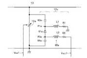
図1に示す非接触型電力伝送システム(以下、単に「電力伝送システム」ともいう)1は、一例として送電装置2および受電装置3を備えて構成され、送電装置2が受電装置3に対して非接触で電力を伝送し、受電装置3が送電装置2から受電した電力を負荷(本例では、一例としてバッテリ)4に対して出力する。  A contactless power transmission system (hereinafter also simply referred to as “power transmission system”) 1 illustrated in FIG. 1 includes apower transmission device 2 and apower reception device 3 as an example, and thepower transmission device 2 is connected to thepower reception device 3. The power is transmitted in a non-contact manner, and the power received by thepower receiving device 3 from thepower transmitting device 2 is output to the load (in this example, a battery as an example) 4.

送電装置2は、信号発生部11、送信アンテナ12、第1整合部13、電力計測部14および第1処理部15を備えて構成されている。信号発生部11は、交流信号S1(本例では一例として、周波数f(数MHzから数十MHz。一例として、13.56MHz)の交流信号を発生して出力する。また、信号発生部11は、第1処理部15によって制御されて、交流信号S1の出力電力値を変更可能に構成されている。  Thepower transmission device 2 includes asignal generation unit 11, atransmission antenna 12, afirst matching unit 13, apower measurement unit 14, and afirst processing unit 15. Thesignal generator 11 generates and outputs an AC signal S1 (in this example, as an example, an AC signal having a frequency f (several MHz to several tens of MHz; as an example, 13.56 MHz). Controlled by thefirst processing unit 15, the output power value of the AC signal S1 can be changed.

送信アンテナ12は、一例としてコイル形状(つるまきバネ形状や平面コイル形状)に形成されている。また、送信アンテナ12は、交流信号S1の供給を受けて電磁場を発生させて、受電装置3に配設された後述の受信アンテナ21と電磁結合する。  As an example, thetransmission antenna 12 is formed in a coil shape (a helical spring shape or a planar coil shape). In addition, thetransmission antenna 12 is supplied with the AC signal S <b> 1, generates an electromagnetic field, and is electromagnetically coupled to a later-describedreception antenna 21 provided in thepower receiving device 3.

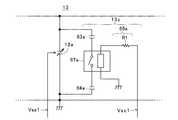
第1整合部(整合部)13は、信号発生部11と送信アンテナ12との間に配設されて(具体的には、信号発生部11と送信アンテナ12とを接続する伝送路に介装されて)、受信アンテナ21との間の距離に応じて変化する送信アンテナ12のインピーダンス(入力インピーダンス)に信号発生部11側のインピーダンスを整合させる(信号発生部11と送信アンテナ12とを整合状態に移行させる)。  The first matching unit (matching unit) 13 is disposed between thesignal generation unit 11 and the transmission antenna 12 (specifically, installed in a transmission path connecting thesignal generation unit 11 and the transmission antenna 12). The impedance on thesignal generating unit 11 side is matched with the impedance (input impedance) of the transmittingantenna 12 that changes according to the distance between the receivingantenna 21 and thesignal generating unit 11 and the transmittingantenna 12 are matched. ).

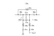
本例では、一例として、第1整合部13は、図3に示すように、送信アンテナ12に対して並列に接続された可変コンデンサ回路13aと、送信アンテナ12に対して直列(具体的には、送信アンテナ12および可変コンデンサ回路13aからなる並列回路に対して直列)に接続された可変コンデンサ回路13bとを備えて構成されている。また、第1整合部13は、可変コンデンサ回路13a,13bの各静電容量値が第1処理部15から出力される制御電圧Vsa1,Vsb1(逆バイアス電圧である直流電圧)によって別個独立して制御されることにより、送信アンテナ12(詳しくは、信号発生部11側から見た送信アンテナ12の入力インピーダンス)と信号発生部11(詳しくは、送信アンテナ12側から見た信号発生部11側の出力インピーダンス)とを整合可能となっている。  In this example, as an example, as shown in FIG. 3, thefirst matching unit 13 includes avariable capacitor circuit 13 a connected in parallel to thetransmission antenna 12 and a series (specifically, the transmission antenna 12). And avariable capacitor circuit 13b connected in series to a parallel circuit including thetransmission antenna 12 and thevariable capacitor circuit 13a. Further, thefirst matching unit 13 is configured so that the capacitance values of thevariable capacitor circuits 13a and 13b are independently determined by the control voltages Vsa1 and Vsb1 (DC voltages that are reverse bias voltages) output from thefirst processing unit 15. By being controlled, the transmitting antenna 12 (specifically, the input impedance of the transmittingantenna 12 viewed from thesignal generating unit 11 side) and the signal generating unit 11 (specifically, thesignal generating unit 11 side viewed from the transmittingantenna 12 side). Output impedance).

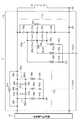
具体的には、可変コンデンサ回路13aは、図5に示すように、ダイオード回路DCa、小型電子部品である2つのコンデンサ35a,36a、小型電子部品である1つのインダクタ37a、小型電子部品である3つのインダクタ38a,39a,40a、および小型電子部品である3つの抵抗41a,42a,43aを備えている。この場合、ダイオード回路DCaは、小型電子部品である可変容量ダイオードとしてのダイオード31aで構成された第1副ダイオード回路DCa1、および小型電子部品である可変容量ダイオードとしてのダイオード32aで構成された第2副ダイオード回路DCa2を備えている。第1副ダイオード回路DCa1は、1つのダイオード31a、または互いに順方向で並列接続(カソード端子同士が接続されると共にアノード端子同士が接続)された複数のダイオード31aで構成されている。第2副ダイオード回路DCa2は、1つのダイオード32a、または互いに順方向で並列接続された複数のダイオード32aで構成されている。また、このようにして構成された第1副ダイオード回路DCa1および第2副ダイオード回路DCa2は、対向して直列接続(カソード端子同士が接続されるか、またはアノード端子同士が接続。本例では、カソード端子同士が接続)されている。ダイオード31aおよびダイオード32a、並びに後述するダイオード31bおよびダイオード32bとしては、ショットキーバリアダイオードやファーストリカバリーダイオードが使用される。  Specifically, as shown in FIG. 5, thevariable capacitor circuit 13a includes a diode circuit DCa, twocapacitors 35a and 36a that are small electronic components, oneinductor 37a that is a small electronic component, and 3 that is a small electronic component. Twoinductors 38a, 39a, and 40a and threeresistors 41a, 42a, and 43a, which are small electronic components, are provided. In this case, the diode circuit DCa is composed of a first sub-diode circuit DCa1 composed of adiode 31a as a variable capacitance diode which is a small electronic component, and asecond diode 32a composed of a variable capacitance diode which is a small electronic component. A sub-diode circuit DCa2 is provided. The first sub-diode circuit DCa1 is configured by onediode 31a or a plurality ofdiodes 31a connected in parallel in the forward direction (the cathode terminals are connected to each other and the anode terminals are connected to each other). The second sub-diode circuit DCa2 includes onediode 32a or a plurality ofdiodes 32a connected in parallel to each other in the forward direction. Further, the first sub-diode circuit DCa1 and the second sub-diode circuit DCa2 thus configured are connected in series facing each other (the cathode terminals are connected to each other or the anode terminals are connected to each other. In this example, The cathode terminals are connected). As thediode 31a and thediode 32a, and thediode 31b and thediode 32b described later, a Schottky barrier diode or a fast recovery diode is used.

コンデンサ35aは、一端がダイオード回路DCaの一端(各ダイオード31aのアノード端子)に接続されると共に、他端が可変コンデンサ回路13aの一端として、可変コンデンサ回路13bおよび送信アンテナ12に接続されている。コンデンサ36aは、一端がダイオード回路DCaの他端(各ダイオード32aのアノード端子)に接続されると共に、他端が可変コンデンサ回路13aの他端として、送電装置2の基準電位(本例では一例としてグランド電位)に接続されている。この構成により、2つのコンデンサ35a,36aは、ダイオード回路DCaに対してそれぞれ直列に接続されている。  One end of thecapacitor 35a is connected to one end of the diode circuit DCa (the anode terminal of eachdiode 31a), and the other end is connected to thevariable capacitor circuit 13b and thetransmission antenna 12 as one end of thevariable capacitor circuit 13a. Thecapacitor 36a has one end connected to the other end of the diode circuit DCa (the anode terminal of eachdiode 32a) and the other end as the other end of thevariable capacitor circuit 13a. Ground potential). With this configuration, the twocapacitors 35a and 36a are respectively connected in series to the diode circuit DCa.

また、各コンデンサ35a,36aは、可変コンデンサ回路13aのダイオード回路DCaに印加される制御電圧Vsa1が可変コンデンサ回路13aの外部に漏洩する事態を防止するための直流カット用コンデンサであり、交流信号S1の周波数fにおけるインピーダンスが、ダイオード回路DCaのインピーダンスに対して十分に小さくなる静電容量値に規定されている(一例として、ダイオード回路DCaの合成容量値の2倍以上の静電容量値に規定されている)。  Thecapacitors 35a and 36a are DC cut capacitors for preventing the control voltage Vsa1 applied to the diode circuit DCa of thevariable capacitor circuit 13a from leaking to the outside of thevariable capacitor circuit 13a, and the AC signal S1. Is defined as a capacitance value that is sufficiently smaller than the impedance of the diode circuit DCa (for example, a capacitance value that is twice or more the combined capacitance value of the diode circuit DCa). Have been).

インダクタ37aは、一端がコンデンサ35aの他端に接続されると共に、他端がコンデンサ36aの他端に接続されている。この構成により、インダクタ37aは、ダイオード回路DCaに対して並列に、具体的には、コンデンサ35a,36aおよびダイオード回路DCaの直列回路に対して並列に並列インダクタとして接続されている。このインダクタ37aは、後述するように、制御電圧Vsa1によって変化させられる可変コンデンサ回路13aの静電容量値Ctp1についての容量変更範囲の下限値を引き下げる機能を有している。  Theinductor 37a has one end connected to the other end of thecapacitor 35a and the other end connected to the other end of thecapacitor 36a. With this configuration, theinductor 37a is connected as a parallel inductor in parallel with the diode circuit DCa, specifically, in parallel with the series circuit of thecapacitors 35a and 36a and the diode circuit DCa. As will be described later, theinductor 37a has a function of lowering the lower limit value of the capacitance change range for the capacitance value Ctp1 of thevariable capacitor circuit 13a that is changed by the control voltage Vsa1.

インダクタ38aおよび抵抗41aは、互いに直列に接続されて、ダイオード回路DCaの一端と基準電位との間に配設されている。インダクタ39aおよび抵抗42aは、互いに直列に接続されて、ダイオード回路DCaの他端と基準電位との間に配設されている。インダクタ40aおよび抵抗43aは、互いに直列に接続されて、これらの直列回路の一端(本例では一例としてインダクタ40a側の端部)が、ダイオード回路DCaにおける第1副ダイオード回路DCa1および第2副ダイオード回路DCa2の接続点CNa(本例では、各ダイオード31a,32aのカソード端子)に接続されている。また、インダクタ40aおよび抵抗43aの直列回路は、処理部15から出力される制御電圧Vsa1を、ダイオード回路DCaの接続点CNaに供給する。  Theinductor 38a and theresistor 41a are connected in series with each other and are disposed between one end of the diode circuit DCa and the reference potential. Theinductor 39a and theresistor 42a are connected in series with each other and are disposed between the other end of the diode circuit DCa and the reference potential. Theinductor 40a and theresistor 43a are connected in series with each other, and one end of these series circuits (in this example, the end on theinductor 40a side) is the first sub-diode circuit DCa1 and the second sub-diode in the diode circuit DCa. The connection point CNa of the circuit DCa2 (in this example, the cathode terminal of each of thediodes 31a and 32a) is connected. The series circuit of theinductor 40a and theresistor 43a supplies the control voltage Vsa1 output from theprocessing unit 15 to the connection point CNa of the diode circuit DCa.

また、各インダクタ38a,39a,40aは、交流信号S1の周波数fにおけるインピーダンスが十分に高くなるようにインダクタンス値が規定されて、交流信号S1の基準電位、および制御電圧Vsa1が供給される供給ラインへの交流信号S1の漏洩を低減する機能を有している。また、各抵抗41a,42a,43aは、制御電圧Vsa1の供給状態において、各インダクタ38a,39a,40aや、各ダイオード31a,32aに流れる電流、および制御電圧Vsa1が供給される供給ラインに流れる直流電流を制限する機能を有している。  Theinductors 38a, 39a, and 40a have an inductance value defined so that the impedance at the frequency f of the AC signal S1 is sufficiently high, and are supplied with the reference potential of the AC signal S1 and the control voltage Vsa1. Has a function of reducing leakage of the alternating current signal S1. Theresistors 41a, 42a, 43a are connected to theinductors 38a, 39a, 40a, the currents flowing through thediodes 31a, 32a, and the direct currents flowing through the supply lines to which the control voltage Vsa1 is supplied in the supply state of the control voltage Vsa1. It has a function to limit current.

以上のように構成された可変コンデンサ回路13aでは、直流電圧としての制御電圧Vsa1が、インダクタ40aおよび抵抗43aの直列回路を介して、第1副ダイオード回路DCa1および第2副ダイオード回路DCa2のそれぞれに、逆バイアスとなる極性で供給(印加)される。ダイオード31a,31bは、逆バイアス電圧に応じて端子間容量値を変化させる特性を有している。したがって、ダイオード回路DCaの容量値(各副ダイオード回路DCa1,DCa2の合成容量値)が制御電圧Vsa1の電圧値に応じて変化するため、可変コンデンサ回路13aの静電容量値Ctp1もまた制御電圧Vsa1の電圧値に応じて変化する。  In thevariable capacitor circuit 13a configured as described above, the control voltage Vsa1 as a DC voltage is applied to each of the first sub-diode circuit DCa1 and the second sub-diode circuit DCa2 via the series circuit of theinductor 40a and theresistor 43a. , And supplied (applied) with a reverse bias polarity. Thediodes 31a and 31b have a characteristic of changing the inter-terminal capacitance value according to the reverse bias voltage. Therefore, since the capacitance value of the diode circuit DCa (the combined capacitance value of the sub-diode circuits DCa1 and DCa2) changes according to the voltage value of the control voltage Vsa1, the capacitance value Ctp1 of thevariable capacitor circuit 13a is also controlled by the control voltage Vsa1. It changes according to the voltage value.

他の可変コンデンサ回路13bも、図5に示すように、上記した可変コンデンサ回路13aのダイオード回路DCa、2つのコンデンサ35a,36a、1つのインダクタ37a、3つのインダクタ38a,39a,40a、および3つの抵抗41a,42a,43aにそれぞれ対応するダイオード回路DCb、2つのコンデンサ35b,36b、1つのインダクタ37b、3つのインダクタ38b,39b,40b、および3つの抵抗41b,42b,43bを備え、可変コンデンサ回路13aと同一に構成されている。このため、可変コンデンサ回路13bの各構成要素の機能であって、対応する可変コンデンサ回路13aの構成要素と同一の機能については説明を省略する。  As shown in FIG. 5, the othervariable capacitor circuit 13b also includes a diode circuit DCa, twocapacitors 35a, 36a, oneinductor 37a, threeinductors 38a, 39a, 40a, and three A variable capacitor circuit including a diode circuit DCb, twocapacitors 35b and 36b, oneinductor 37b, threeinductors 38b, 39b and 40b, and threeresistors 41b, 42b and 43b respectively corresponding to theresistors 41a, 42a and 43a The configuration is the same as 13a. Therefore, the description of the function of each component of thevariable capacitor circuit 13b, which is the same as the corresponding component of thevariable capacitor circuit 13a, is omitted.

この場合、ダイオード回路DCbは、可変容量ダイオードとしてのダイオード31bで構成された第1副ダイオード回路DCb1、および可変容量ダイオードとしてのダイオード32bで構成された第2副ダイオード回路DCb2を備えている。第1副ダイオード回路DCb1は、1つのダイオード31b、または互いに順方向で並列接続された複数のダイオード31bで構成されている。第2副ダイオード回路DCb2は、1つのダイオード32b、または互いに順方向で並列接続された複数のダイオード32bで構成されている。また、第1副ダイオード回路DCb1および第2副ダイオード回路DCb2は、対向して直列接続されている。  In this case, the diode circuit DCb includes a first sub-diode circuit DCb1 constituted by adiode 31b as a variable capacitance diode, and a second sub-diode circuit DCb2 constituted by adiode 32b as a variable capacitance diode. The first sub-diode circuit DCb1 includes asingle diode 31b or a plurality ofdiodes 31b connected in parallel to each other in the forward direction. The second sub-diode circuit DCb2 includes onediode 32b or a plurality ofdiodes 32b connected in parallel to each other in the forward direction. The first sub-diode circuit DCb1 and the second sub-diode circuit DCb2 are connected in series so as to face each other.

コンデンサ35bは、一端がダイオード回路DCbの一端(各ダイオード31bのアノード端子)に接続されると共に、他端が可変コンデンサ回路13bの一端として、電力計測部14に接続されている。コンデンサ36bは、一端がダイオード回路DCbの他端(各ダイオード32bのアノード端子)に接続されると共に、他端が可変コンデンサ回路13bの他端として、可変コンデンサ回路13aの一端に接続されている。この構成により、2つのコンデンサ35b,36bは、ダイオード回路DCbに対してそれぞれ直列に接続されている。  One end of thecapacitor 35b is connected to one end of the diode circuit DCb (the anode terminal of eachdiode 31b), and the other end is connected to thepower measuring unit 14 as one end of thevariable capacitor circuit 13b. One end of thecapacitor 36b is connected to the other end of the diode circuit DCb (the anode terminal of eachdiode 32b), and the other end is connected to one end of thevariable capacitor circuit 13a as the other end of thevariable capacitor circuit 13b. With this configuration, the twocapacitors 35b and 36b are respectively connected in series to the diode circuit DCb.

インダクタ37bは、一端がコンデンサ35bの他端に接続されると共に、他端がコンデンサ36bの他端に接続されている。この構成により、インダクタ37bは、ダイオード回路DCbに対して並列に、具体的には、コンデンサ35b,36bおよびダイオード回路DCbの直列回路に対して並列に並列インダクタとして接続されている。  Theinductor 37b has one end connected to the other end of thecapacitor 35b and the other end connected to the other end of thecapacitor 36b. With this configuration, theinductor 37b is connected as a parallel inductor in parallel with the diode circuit DCb, specifically, in parallel with the series circuit of thecapacitors 35b and 36b and the diode circuit DCb.

インダクタ38bおよび抵抗41bは、互いに直列に接続されて、ダイオード回路DCbの一端と基準電位との間に配設されている。インダクタ39bおよび抵抗42bは、互いに直列に接続されて、ダイオード回路DCbの他端と基準電位との間に配設されている。インダクタ40bおよび抵抗43bは、互いに直列に接続されて、これらの直列回路の一端(本例では一例としてインダクタ40b側の端部)が、ダイオード回路DCbにおける第1副ダイオード回路DCb1および第2副ダイオード回路DCb2の接続点CNb(本例では、各ダイオード31b,32bのカソード端子)に接続されている。また、インダクタ40bおよび抵抗43bの直列回路は、処理部15から出力される制御電圧Vsb1を、ダイオード回路DCbの接続点CNbに供給する。  Theinductor 38b and theresistor 41b are connected in series with each other and are disposed between one end of the diode circuit DCb and the reference potential. Theinductor 39b and theresistor 42b are connected in series with each other and are disposed between the other end of the diode circuit DCb and the reference potential. Theinductor 40b and theresistor 43b are connected to each other in series, and one end of these series circuits (in this example, the end on theinductor 40b side) is the first sub-diode circuit DCb1 and the second sub-diode in the diode circuit DCb. The connection point CNb of the circuit DCb2 (in this example, the cathode terminal of each of thediodes 31b and 32b) is connected. The series circuit of theinductor 40b and theresistor 43b supplies the control voltage Vsb1 output from theprocessing unit 15 to the connection point CNb of the diode circuit DCb.

以上のように構成された可変コンデンサ回路13bでは、直流電圧としての制御電圧Vsb1が、インダクタ40bおよび抵抗43bの直列回路を介して、第1副ダイオード回路DCb1および第2副ダイオード回路DCb2のそれぞれに、逆バイアスとなる極性で供給(印加)される。したがって、ダイオード回路DCbの容量値(各副ダイオード回路DCb1,DCb2の合成容量値)が制御電圧Vsb1の電圧値に応じて変化するため、可変コンデンサ回路13bの静電容量値Cts1もまた制御電圧Vsb1の電圧値に応じて変化する。  In thevariable capacitor circuit 13b configured as described above, the control voltage Vsb1 as a DC voltage is applied to each of the first sub-diode circuit DCb1 and the second sub-diode circuit DCb2 via the series circuit of theinductor 40b and theresistor 43b. , And supplied (applied) with a reverse bias polarity. Accordingly, since the capacitance value of the diode circuit DCb (the combined capacitance value of the sub-diode circuits DCb1 and DCb2) changes according to the voltage value of the control voltage Vsb1, the electrostatic capacitance value Cts1 of thevariable capacitor circuit 13b is also controlled by the control voltage Vsb1. It changes according to the voltage value.

電力計測部14は、図1に示すように、信号発生部11と第1整合部13との間に配設されて(具体的には、信号発生部11と第1整合部13とを接続する伝送路に介装されて)、信号発生部11から第1整合部13側への交流信号S1についての進行波の電力値(進行波電力値)W2aと、第1整合部13から信号発生部11側に戻る交流信号S1についての反射波の電力値(反射波電力値)W2bとを計測して電力情報として第1処理部15に出力する。  As shown in FIG. 1, thepower measuring unit 14 is disposed between thesignal generating unit 11 and the first matching unit 13 (specifically, thesignal generating unit 11 and thefirst matching unit 13 are connected to each other). Generated in the transmission line), the traveling wave power value (traveling wave power value) W2a for the AC signal S1 from thesignal generating unit 11 to thefirst matching unit 13 side, and thefirst matching unit 13 generates a signal. The power value (reflected wave power value) W2b of the reflected wave for the AC signal S1 returning to theunit 11 side is measured and output to thefirst processing unit 15 as power information.

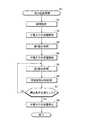
第1処理部15は、一例としてCPUおよび内部メモリ(いずれも図示せず)を含んで構成されて、信号発生部11に対する制御処理と、第1整合部13を制御して信号発生部11(具体的には電力計測部14および信号発生部11)と送信アンテナ12との間を整合状態に移行させる整合処理を含む電力伝送処理50(図2参照)とを実行する。  As an example, thefirst processing unit 15 includes a CPU and an internal memory (both not shown), and controls thesignal generating unit 11 and controls thefirst matching unit 13 to control the signal generating unit 11 ( Specifically, a power transmission process 50 (see FIG. 2) including a matching process for shifting thepower measurement unit 14 and the signal generation unit 11) and thetransmission antenna 12 to a matching state is executed.

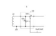
受電装置3は、受信アンテナ21、第2整合部22、整流部23および第2処理部24を備えて構成されている。受信アンテナ21は、一例として送信アンテナ12と同一のコイル形状に形成されて、送信アンテナ12と同一のインダクタンスに規定されている。また、受信アンテナ21は、送電装置2の送信アンテナ12と電磁結合して(つまり、送信アンテナ12によって発生させられた電磁場により)、その両端間に誘導電圧V1を発生させる。第2整合部22は、受信アンテナ21と整流部23との間に配設されて(具体的には、受信アンテナ21と整流部23とを接続する伝送路に介装されて)、受信アンテナ21のインピーダンス(出力インピーダンス)と整流部23側のインピーダンスとを整合させる(受信アンテナ21と整流部23とを整合状態に移行させる)。  Thepower receiving device 3 includes a receivingantenna 21, asecond matching unit 22, a rectifyingunit 23, and asecond processing unit 24. The receivingantenna 21 is formed in the same coil shape as the transmittingantenna 12 as an example, and is defined by the same inductance as the transmittingantenna 12. Thereception antenna 21 is electromagnetically coupled to thetransmission antenna 12 of the power transmission device 2 (that is, due to an electromagnetic field generated by the transmission antenna 12), and generates an induced voltage V1 between both ends thereof. Thesecond matching unit 22 is disposed between the receivingantenna 21 and the rectifying unit 23 (specifically, interposed in a transmission path connecting the receivingantenna 21 and the rectifying unit 23), and the receiving antenna. The impedance of 21 (output impedance) is matched with the impedance on the rectifyingunit 23 side (the receivingantenna 21 and the rectifyingunit 23 are shifted to the matching state).

本例では、一例として、第2整合部22は、図4に示すように、受信アンテナ21に対して並列に接続された可変コンデンサ回路22aと、受信アンテナ21に対して直列(すなわち、受信アンテナ21および可変コンデンサ回路22aからなる並列回路に対して直列)に接続された可変コンデンサ回路22bとを備えている。本例では一例として、図示はしないが、可変コンデンサ回路22aは、第1整合部13の可変コンデンサ回路13aと同一に構成され、可変コンデンサ回路22bは、第1整合部13の可変コンデンサ回路13bと同一に構成されている。また、第2整合部22は、可変コンデンサ回路22a,22bの各静電容量値Ctp2,Cts2が第2処理部24から出力される制御電圧Vsa2,Vsb2(逆バイアス電圧である直流電圧)によって別個独立して制御されることにより、受信アンテナ21(詳しくは、整流部23側から見た受信アンテナ21の出力インピーダンス)と整流部23(詳しくは、受信アンテナ21側から見た整流部23の入力インピーダンス)とを整合可能となっている。  In this example, as an example, as shown in FIG. 4, thesecond matching unit 22 includes a variable capacitor circuit 22 a connected in parallel to thereception antenna 21 and a series connection to the reception antenna 21 (that is, the reception antenna). 21 and avariable capacitor circuit 22b connected in series to a parallel circuit composed of the variable capacitor circuit 22a. In this example, as an example, although not shown, the variable capacitor circuit 22a is configured the same as thevariable capacitor circuit 13a of thefirst matching unit 13, and thevariable capacitor circuit 22b includes thevariable capacitor circuit 13b of thefirst matching unit 13. It is configured identically. Further, in thesecond matching unit 22, the electrostatic capacitance values Ctp2 and Cts2 of thevariable capacitor circuits 22a and 22b are separately determined by the control voltages Vsa2 and Vsb2 (DC voltages that are reverse bias voltages) output from thesecond processing unit 24. By being controlled independently, the receiving antenna 21 (specifically, the output impedance of the receivingantenna 21 viewed from the rectifyingunit 23 side) and the rectifying unit 23 (specifically, the input of the rectifyingunit 23 viewed from the receivingantenna 21 side). Impedance).

なお、可変コンデンサ回路13a,13bの各静電容量値Ctp1,Cts1と、可変コンデンサ回路22a,22bの各静電容量値Ctp2,Cts2とを特に区別しないときには、アンテナ(送信アンテナ12または受信アンテナ21)と直列に接続される可変コンデンサ回路(可変コンデンサ回路13a,22a)の静電容量値をCtpと表記し、並列に接続される可変コンデンサ回路(可変コンデンサ回路13b,22b)の静電容量値をCtsと表記するものとする。また、制御電圧Vsa1,Vsb1および制御電圧Vsa2,Vsb2についても、特に区別しないときには、制御電圧Vsと表記するものとする。  When it is not particularly necessary to distinguish the capacitance values Ctp1 and Cts1 of thevariable capacitor circuits 13a and 13b from the capacitance values Ctp2 and Cts2 of thevariable capacitor circuits 22a and 22b, the antenna (thetransmission antenna 12 or the reception antenna 21). The capacitance value of the variable capacitor circuit (variable capacitor circuits 13a and 22a) connected in series with C) is denoted as Ctp, and the capacitance value of the variable capacitor circuit (variable capacitor circuits 13b and 22b) connected in parallel. Is expressed as Cts. Further, the control voltages Vsa1, Vsb1 and the control voltages Vsa2, Vsb2 are also expressed as the control voltage Vs unless otherwise distinguished.

整流部23は、電圧生成部の一例であって、受信アンテナ21に生じる誘導電圧V1を第2整合部22を介して入力すると共に、この誘導電圧V1に基づいて、バッテリ4に供給する電圧(本例では直流電圧)Voを生成する。具体的には、整流部23は、整流回路および平滑回路で構成されて、第2整合部22から出力される誘導電圧(交流電圧)V1を整流・平滑して電圧Voを生成すると共に、生成した電圧Voをバッテリ4に出力する。また、本例では、一例として、受電装置3内の各構成要素は、この電圧Voを整流部23から供給されて作動する。なお、整流部23から供給された電圧Voを充電するバッテリを備え(図示せず)、このバッテリの電圧で受電装置3内の各構成要素を作動させてもよい。また、整流部23に代えて、電圧生成部を、例えば、DC−DCコンバータ、AC−DCコンバータ、またはAC−ACコンバータで構成することもできる。  Therectifier 23 is an example of a voltage generator, and receives the induced voltage V1 generated in the receivingantenna 21 via thesecond matching unit 22 and supplies a voltage (to thebattery 4 based on the induced voltage V1) ( In this example, a DC voltage (Vo) is generated. Specifically, the rectifyingunit 23 includes a rectifying circuit and a smoothing circuit, rectifies and smoothes the induced voltage (AC voltage) V1 output from thesecond matching unit 22, and generates the voltage Vo. The voltage Vo thus output is output to thebattery 4. In this example, as an example, each component in thepower receiving device 3 operates by being supplied with this voltage Vo from the rectifyingunit 23. Note that a battery (not shown) that charges the voltage Vo supplied from therectifier 23 may be provided, and each component in thepower receiving device 3 may be operated by the voltage of the battery. Moreover, it can replace with therectifier 23 and can comprise a voltage generation part with a DC-DC converter, an AC-DC converter, or an AC-AC converter, for example.

第2処理部24は、一例としてCPUおよび内部メモリ(いずれも図示せず)を含んで構成されて、第2整合部22を制御して受信アンテナ21とバッテリ4(具体的には整流部23およびバッテリ4)とを上記の整合状態に移行させる整合処理を実行する。  Thesecond processing unit 24 includes, for example, a CPU and an internal memory (both not shown), and controls thesecond matching unit 22 to receive theantenna 21 and the battery 4 (specifically, the rectifying unit 23). And the battery 4) are moved to the above-described matching state.

次に、電力伝送システム1の動作について説明する。一例として、交流信号S1の周波数fは13.56MHzに規定されているものとする。また、各インダクタ38a,39a,40a,38b,39b,40bは、この周波数fでのインピーダンスが十分に高くなるようにインダクタンス値が一例として100μHに規定されているものとする(インピーダンスが約8.5kΩ)。  Next, the operation of thepower transmission system 1 will be described. As an example, it is assumed that the frequency f of the AC signal S1 is defined as 13.56 MHz. Eachinductor 38a, 39a, 40a, 38b, 39b, 40b has an inductance value defined as 100 μH as an example so that the impedance at this frequency f is sufficiently high (impedance is about 8. 5 kΩ).

また、受電装置3では、作動状態に移行した直後に、第2処理部24が、第2整合部22の各可変コンデンサ回路22a,22bに対して、予め規定された直流電圧値の制御電圧Vsa2,Vsb2を出力することにより、各可変コンデンサ回路22a,22bの静電容量値を規定の容量値に設定して、受信アンテナ21と整流部23とを良好な整合状態に移行させて維持するものとする。  Further, in thepower receiving device 3, immediately after shifting to the operating state, thesecond processing unit 24 controls thevariable capacitor circuits 22 a and 22 b of thesecond matching unit 22 to have a control voltage Vsa2 having a predetermined DC voltage value. , Vsb2 to set the capacitance value of eachvariable capacitor circuit 22a, 22b to a specified capacitance value, and the receivingantenna 21 and the rectifyingunit 23 are shifted to a good matching state and maintained. And

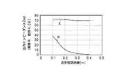
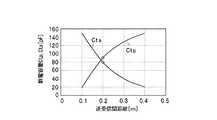
また、送電装置2と、上記のようにして整合状態に移行した受電装置3とが、一例として、0.1m〜0.4mの範囲(以下、「移動範囲」ともいう)内で相対的に移動している状態(送受信間距離が0.1m〜0.4mの範囲内で変化する状態)において、送電装置2が受電装置3に対して電力を伝送するものとする。また、0.1m〜0.4mの範囲内で送受信間距離が変化した状態において、送電装置2における第1整合部13の出力インピーダンスZout(第1整合部13の出力から送信アンテナ12側を見たときの送信アンテナ12以降のインピーダンス)のレジスタンスRとリアクタンスXは、一例として図6に示すように変化する。この場合、0.1m〜0.4mの範囲内で送受信間距離が変化したときに、図6に示すように変化するインピーダンスZoutに対して、図3,5に示す構成の第1整合部13を用いて、信号発生部11側のインピーダンスを整合させるためには、図7に示すように、送受信間距離に応じて、第1整合部13における可変コンデンサ回路13aの静電容量値Ctpを20pF〜150pFの範囲内で、また可変コンデンサ回路13bの静電容量値Ctsを20pF〜150pFの範囲でそれぞれ変化させる必要がある。  In addition, thepower transmission device 2 and thepower reception device 3 that has shifted to the matching state as described above are relatively within a range of 0.1 m to 0.4 m (hereinafter, also referred to as “movement range”) as an example. It is assumed that thepower transmission device 2 transmits power to thepower reception device 3 in a moving state (a state in which the distance between transmission and reception changes within a range of 0.1 m to 0.4 m). Further, in a state where the distance between transmission and reception is changed within the range of 0.1 m to 0.4 m, the output impedance Zout of thefirst matching unit 13 in the power transmission device 2 (see thetransmission antenna 12 side from the output of the first matching unit 13). The resistance R and the reactance X of the impedance after the transmittingantenna 12 change as shown in FIG. 6 as an example. In this case, thefirst matching unit 13 having the configuration shown in FIGS. 3 and 5 with respect to the impedance Zout that changes as shown in FIG. 6 when the distance between transmission and reception changes within the range of 0.1 m to 0.4 m. As shown in FIG. 7, the capacitance value Ctp of thevariable capacitor circuit 13a in thefirst matching unit 13 is set to 20 pF according to the distance between transmission and reception. It is necessary to change the capacitance value Cts of thevariable capacitor circuit 13b within a range of 20 pF to 150 pF.

このため、一例として、可変コンデンサ回路13aにおいて、4つのダイオード31aを並列接続して構成された第1副ダイオード回路DCa1と4つのダイオード32aを並列接続して構成された第2副ダイオード回路DCa2とを使用してダイオード回路DCaを構成し、可変コンデンサ回路13bにおいて、4つのダイオード31bを並列接続して構成された第1副ダイオード回路DCb1と4つのダイオード32bを並列接続して構成された第2副ダイオード回路DCb2とを使用してダイオード回路DCbを構成することで、各可変コンデンサ回路13a,13bの静電容量値Ctp,Ctsについて、上記した範囲で容量値を変更可能としている。また、コンデンサ35a,36a,35b,36bの静電容量値は、各可変コンデンサ回路13a,13bの上記した静電容量値Ctp,Ctsに対して十分に大きな容量値(本例では、一例として4000pF)に規定されている。  For this reason, as an example, in thevariable capacitor circuit 13a, the first sub-diode circuit DCa1 configured by connecting the fourdiodes 31a in parallel and the second sub-diode circuit DCa2 configured by connecting the fourdiodes 32a in parallel. Is used to configure the diode circuit DCa, and in thevariable capacitor circuit 13b, the first sub-diode circuit DCb1 configured by connecting the fourdiodes 31b in parallel and the fourdiodes 32b are connected in parallel. By configuring the diode circuit DCb using the sub-diode circuit DCb2, the capacitance values Ctp and Cts of thevariable capacitor circuits 13a and 13b can be changed in the above-described range. In addition, the capacitance values of thecapacitors 35a, 36a, 35b, and 36b are sufficiently larger than the capacitance values Ctp and Cts of thevariable capacitor circuits 13a and 13b (in this example, 4000 pF as an example). ).

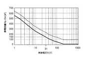
また、制御電圧Vsを1Vから200Vまで変化させたときの可変コンデンサ回路13a,13bの静電容量値Ctp,Ctsは、インダクタ37aやインダクタ37bのない構成では、図8において破線で示すように、639.5pFから95.2pFの範囲内で変化するが、その下限値(95.2pF)は、要求される上記した静電容量値Ctsの下限値20pFには達しない。一方、インダクタ37aやインダクタ37bを有する構成では、インダクタ37a,37bのインダクタンスを1.617μHとすることにより、図8において実線で示すように、制御電圧Vsを1Vから200Vまで変化させたときの静電容量値Ctp,Ctsの下限値を20pF以下(この例では10pF)まで変化させることが可能となる。  Further, when the control voltage Vs is changed from 1 V to 200 V, the capacitance values Ctp and Cts of thevariable capacitor circuits 13a and 13b are as shown by the broken lines in FIG. 8 in the configuration without theinductor 37a and theinductor 37b. Although it changes within the range of 639.5 pF to 95.2 pF, the lower limit value (95.2 pF) does not reach the requiredlower limit value 20 pF of the aforementioned capacitance value Cts. On the other hand, in the configuration including theinductor 37a and theinductor 37b, by setting the inductance of theinductors 37a and 37b to 1.617 μH, the static voltage when the control voltage Vs is changed from 1V to 200V as shown by the solid line in FIG. It becomes possible to change the lower limit values of the capacitance values Ctp and Cts to 20 pF or less (10 pF in this example).

このインダクタ37a,37bのインダクタンスの算出手順について説明する。なお、本例では、図7に示すように、送受信間距離を0.1m以上0.4m以下としたときの可変コンデンサ回路13a,13bの静電容量値Ctp,Ctsについての下限値は20pFであるが、静電容量値Ctp,Ctsの可変範囲の下限値に余裕を持たせるため、可変コンデンサ回路13a,13bの静電容量値Ctp,Ctsについての下限値を10pFまで変化させ得るインダクタンスを算出するものとする。  A procedure for calculating the inductances of theinductors 37a and 37b will be described. In this example, as shown in FIG. 7, the lower limit value of the capacitance values Ctp and Cts of thevariable capacitor circuits 13a and 13b when the distance between transmission and reception is 0.1 m or more and 0.4 m or less is 20 pF. However, in order to give a margin to the lower limit value of the variable range of the capacitance values Ctp and Cts, an inductance that can change the lower limit value of the capacitance values Ctp and Cts of thevariable capacitor circuits 13a and 13b to 10 pF is calculated. It shall be.

まず、インダクタ37a,37bの存在しない場合の静電容量値Ctp,Ctsの下限値は、上記したように95.2pFであり(図8参照)、これを10pFまで引き下げるための容量値の引き下げ幅Csubは、85.2(=95.2−10)pFである。また、この引き下げ幅Csubに相当するリアクタンスXsubは、137.76(=1/(2×π×13.56×10×85.2×10−12)Ωである。これにより、実装するインダクタ37aのインダクタンスは、上記した1.617(=Xsub/(2×π×13.56×10))μHと算出される。First, the lower limit value of the capacitance values Ctp and Cts in the absence of theinductors 37a and 37b is 95.2 pF as described above (see FIG. 8), and the capacitance value reduction range for reducing this to 10 pF. Csub is 85.2 (= 95.2-10) pF. In addition, the reactance Xsub corresponding to the reduction width Csub is 137.76 (= 1 / (2 × π × 13.56 × 106 × 85.2 × 10−12 ) Ω. The inductance of 37a is calculated as 1.617 (= Xsub / (2 × π × 13.56 × 10⁶ )) μH described above.

また、可変コンデンサ回路13a,13bと同一に構成されている可変コンデンサ回路22a,22bについても、これらに並列に接続されるインダクタ(図示せず)のインダクタンス値が上記したインダクタンス37a,37bと同様にして規定されている。  In addition, for thevariable capacitor circuits 22a and 22b configured in the same manner as thevariable capacitor circuits 13a and 13b, the inductance values of inductors (not shown) connected in parallel to these are the same as theinductances 37a and 37b described above. It is prescribed.

また、本例の可変コンデンサ回路13aは、第1副ダイオード回路DCa1と第2副ダイオード回路DCa2とを対向した状態で直列接続して構成されたダイオード回路DCaを有し、可変コンデンサ回路13bは、第1副ダイオード回路DCb1と第2副ダイオード回路DCb2とを対向した状態で直列接続して構成されたダイオード回路DCbを有している。このため、入力された交流信号S1は、1/2に分圧された状態で各ダイオード31a,32a,31b,32bに印加される。また、各ダイオード31a,32a,31b,32bが可変容量ダイオードとして機能するためには、この分圧されて印加されている交流信号S1よりも高い制御電圧Vsa1,Vsb1が印加されることにより、逆バイアス状態に維持されている必要がある。  In addition, thevariable capacitor circuit 13a of this example includes a diode circuit DCa configured by connecting the first sub-diode circuit DCa1 and the second sub-diode circuit DCa2 in series with each other facing each other, and thevariable capacitor circuit 13b includes: The first sub-diode circuit DCb1 and the second sub-diode circuit DCb2 have a diode circuit DCb configured in series in a state of being opposed to each other. For this reason, the input AC signal S1 is applied to each of thediodes 31a, 32a, 31b, and 32b in a state of being divided into ½. Further, in order for each of thediodes 31a, 32a, 31b, and 32b to function as a variable capacitance diode, the control voltages Vsa1 and Vsb1 higher than the divided and applied AC signal S1 are applied. It must be maintained in a biased state.

また、第1処理部15および第2処理部24は、一例として図8に示す制御電圧Vsの可変範囲のうちの31Vから200Vの範囲内で制御電圧Vsを変化させる。これにより、図8に示すように、第1処理部15および第2処理部24は、可変コンデンサ回路13a,13bについての静電容量値Ctp,Ctsを10pF以上150pF以下の範囲で変化させる。また、信号発生部11から出力される交流信号S1の電力を約50Wまで高めたとしても、制御電圧Vsの下限電圧値が31Vであるため、この制御電圧Vsによって各ダイオード31a,32a,31b,32bは常に逆バイアス状態に維持されることが、シミュレーションによって確認されている。  Moreover, the1st process part 15 and the2nd process part 24 change the control voltage Vs within the range of 31V to 200V of the variable range of the control voltage Vs shown in FIG. 8 as an example. Thereby, as shown in FIG. 8, the1st process part 15 and the2nd process part 24 change the electrostatic capacitance values Ctp and Cts aboutvariable capacitor circuit 13a, 13b in the range of 10 pF or more and 150 pF or less. Further, even if the power of the AC signal S1 output from thesignal generator 11 is increased to about 50 W, the lower limit voltage value of the control voltage Vs is 31 V. Therefore, eachdiode 31a, 32a, 31b, It has been confirmed by simulation that 32b is always maintained in the reverse bias state.

以上のように構成された電力伝送システム1では、上記したように、まず、受電装置3が、受信アンテナ21と整流部23とが整合する整合状態に移行する。次いで、送電装置2では、第1処理部15が、図2に示す電力伝送処理50を実行する。この電力伝送処理50では、第1処理部15は、最初に、予め規定されている初期電圧での制御電圧Vsa1,Vsb1の出力を開始して、第1整合部13の各可変コンデンサ回路13a,13bを予め規定された静電容量値Ctp,Ctsに初期設定する(ステップ51)。具体的には、送電装置2に対する受電装置3の距離(送受信間距離)が、0.1mから0.4mの範囲内の特定の距離であるとしたときに、送電装置2を受電装置3に整合させるに必要な容量値に各可変コンデンサ回路13a,13bの静電容量値Ctp,Ctsを設定する。例えば、図7に示すように、この特定の距離が0.2mであるとしたときの静電容量値Ctp(=90pF)および静電容量値Cts(=80pF)に設定する。  In thepower transmission system 1 configured as described above, as described above, first, thepower receiving device 3 shifts to a matching state in which the receivingantenna 21 and the rectifyingunit 23 are matched. Next, in thepower transmission device 2, thefirst processing unit 15 executes thepower transmission process 50 illustrated in FIG. In thepower transmission process 50, thefirst processing unit 15 first starts outputting the control voltages Vsa1 and Vsb1 at a predetermined initial voltage, and eachvariable capacitor circuit 13a, 13b is initially set to predetermined capacitance values Ctp and Cts (step 51). Specifically, when the distance (inter-transmission / reception distance) of thepower receiving device 3 to thepower transmitting device 2 is a specific distance within a range of 0.1 m to 0.4 m, thepower transmitting device 2 is connected to thepower receiving device 3. The capacitance values Ctp and Cts of thevariable capacitor circuits 13a and 13b are set to the capacitance values necessary for matching. For example, as shown in FIG. 7, the capacitance value Ctp (= 90 pF) and the capacitance value Cts (= 80 pF) when the specific distance is 0.2 m are set.

次いで、第1処理部15は、小電力での電力の伝送(送電)を開始する(ステップ52)。具体的には、第1処理部15は、信号発生部11に対する制御処理を実行して、交流信号S1を小電力(例えば、1W以下)で出力させる。これにより、信号発生部11から出力された交流信号S1が、電力計測部14および第1整合部13を経由して送信アンテナ12に供給されて、小電力での送電が開始される。電力計測部14は、交流信号S1についての進行波電力値W2aおよび反射波電力値W2bの計測と、計測した各電力値W2a,W2bの第1処理部15への出力とを開始する。  Next, thefirst processing unit 15 starts power transmission (power transmission) with low power (step 52). Specifically, the1st process part 15 performs the control process with respect to thesignal generation part 11, and outputs alternating current signal S1 with small electric power (for example, 1 W or less). As a result, the AC signal S1 output from thesignal generation unit 11 is supplied to thetransmission antenna 12 via thepower measurement unit 14 and thefirst matching unit 13, and transmission with low power is started. Thepower measuring unit 14 starts measuring the traveling wave power value W2a and the reflected wave power value W2b for the AC signal S1, and outputting the measured power values W2a and W2b to thefirst processing unit 15.

続いて、第1処理部15は、第1整合処理を開始する(ステップ53)。この第1整合処理では、第1処理部15は、電力計測部14から出力される反射波電力値W2bを取得しつつ、反射波電力値W2bが予め規定された閾値(小電力の送電での閾値。以下、「第1閾値」ともいう)以下となるように、第1整合部13への各制御電圧Vsa1,Vsb1を変化させる(連続的に変化させる)ことにより、各可変コンデンサ回路13a,13bの静電容量値Ctp,Ctsを連続的に変化させる。この電力伝送システム1では、第1整合部13の各可変コンデンサ回路13a,13bがダイオード31a,32a,31a,32aで構成されており、各制御電圧Vsa1,Vsb1の変化に応じて、瞬時にそれらの静電容量値Ctp,Ctsを変化させる(変更する)ことが可能となっている。このため、第1処理部15は、反射波電力値W2bが第1閾値以下となる状態、つまり、送電装置2と受電装置3とが整合する状態に第1整合部13を極めて短時間で移行させる。  Subsequently, thefirst processing unit 15 starts the first matching process (step 53). In the first matching process, thefirst processing unit 15 obtains the reflected wave power value W2b output from thepower measuring unit 14, while the reflected wave power value W2b is defined in advance as a predetermined threshold (low power transmission). Threshold value (hereinafter also referred to as “first threshold value”). By changing (continuously changing) the control voltages Vsa1 and Vsb1 to thefirst matching unit 13, eachvariable capacitor circuit 13a, The capacitance values Ctp and Cts of 13b are continuously changed. In thispower transmission system 1, each of thevariable capacitor circuits 13a and 13b of thefirst matching unit 13 is composed ofdiodes 31a, 32a, 31a, and 32a, and instantly according to changes in the control voltages Vsa1 and Vsb1. It is possible to change (change) the electrostatic capacitance values Ctp and Cts. Therefore, thefirst processing unit 15 shifts thefirst matching unit 13 in a very short time to a state where the reflected wave power value W2b is equal to or lower than the first threshold, that is, a state where thepower transmission device 2 and thepower reception device 3 are matched. Let

なお、送電装置2と受電装置3との間の距離(送受信間距離)の変化に伴い、送電装置2と受電装置3との整合状態も変化し、電力計測部14から出力される反射波電力値W2bも変化する。このため、第1処理部15は、上記した第1整合処理を繰り返し実行して、第1整合部13への各制御電圧Vsa1,Vsb1をリアルタイムに連続的に変化させる(変更する)ことによって各可変コンデンサ回路13a,13bの静電容量値Ctp,Ctsをリアルタイムに連続的に変化させて、第1閾値以下となるように反射波電力値W2bを維持する。  In addition, with the change of the distance (distance between transmission and reception) between thepower transmission device 2 and thepower reception device 3, the matching state between thepower transmission device 2 and thepower reception device 3 also changes, and the reflected wave power output from thepower measurement unit 14 The value W2b also changes. For this reason, thefirst processing unit 15 repeatedly executes the first matching process described above to continuously change (change) the control voltages Vsa1 and Vsb1 to thefirst matching unit 13 in real time. The electrostatic capacitance values Ctp and Cts of thevariable capacitor circuits 13a and 13b are continuously changed in real time to maintain the reflected wave power value W2b so as to be equal to or lower than the first threshold value.

次いで、第1処理部15は、中電力での電力の伝送(送電)を開始する(ステップ54)。具体的には、第1処理部15は、信号発生部11に対する制御を実行して、交流信号S1を中電力(例えば、1Wを超え、数十Wまでの電力。本例では一例として50W)で出力させる。これにより、信号発生部11から出力された交流信号S1が送信アンテナ12に供給されて、中電力での送電が開始される。  Next, thefirst processing unit 15 starts transmission (power transmission) of medium power (step 54). Specifically, the1st processing part 15 performs control with respect to thesignal generation part 11, and makes alternating current signal S1 medium electric power (for example, electric power exceeding 1W and several dozen W. In this example, it is 50W as an example). To output. As a result, the AC signal S1 output from thesignal generator 11 is supplied to thetransmission antenna 12, and power transmission with medium power is started.

続いて、第1処理部15は、第2整合処理を実行する(ステップ55)。この第2整合処理では、第1処理部15は、電力計測部14から出力される反射波電力値W2bを取得しつつ、反射波電力値W2bが予め規定された閾値(中電力の送電での閾値。以下、「第2閾値」ともいう)以下となるように、第1整合部13への各制御電圧Vsa1,Vsb1を変化させる(つまり、各可変コンデンサ回路13a,13bの静電容量値Ctp,Ctsを変化させる)。この場合においても、第1整合処理のときと同様にして、各制御電圧Vsa1,Vsb1を変化させる(変更する)ことにより、各可変コンデンサ回路13a,13bの静電容量値Ctp,Ctsを瞬時に変化させる(変更する)ことが可能なため、第1処理部15は、反射波電力値W2bが第2閾値以下となる状態、つまり、送電装置2と受電装置3とが整合する状態に第1整合部13を極めて短時間で移行させる。  Subsequently, thefirst processing unit 15 executes a second matching process (step 55). In the second matching process, thefirst processing unit 15 obtains the reflected wave power value W2b output from thepower measuring unit 14, and the reflected wave power value W2b is set to a predetermined threshold value (medium power transmission). Threshold value (hereinafter also referred to as “second threshold value”) The control voltages Vsa1 and Vsb1 to thefirst matching unit 13 are changed so as to be equal to or lower (that is, the capacitance values Ctp of thevariable capacitor circuits 13a and 13b). , Cts). Also in this case, the capacitance values Ctp and Cts of thevariable capacitor circuits 13a and 13b are instantaneously changed by changing (changing) the control voltages Vsa1 and Vsb1 in the same manner as in the first matching process. Since thefirst processing unit 15 can change (change) thefirst processing unit 15 in a state where the reflected wave power value W2b is equal to or lower than the second threshold, that is, in a state where thepower transmission device 2 and thepower reception device 3 are matched. The matchingunit 13 is moved in a very short time.

その後、第1処理部15は、上記した第2整合処理を繰り返し実行して、第1整合部13への各制御電圧Vsa1,Vsb1をリアルタイムに連続的に変化させる(変更する)ことによって各可変コンデンサ回路13a,13bの静電容量値Ctp,Ctsをリアルタイムに連続的に変化させて、第2閾値以下となるように反射波電力値W2bを維持する。これにより、送電装置2と受電装置3との間の距離(送受信間距離)が0.1mから0.4mの範囲内で変化したとしても、送電装置2から受電装置3に対して、中電力での電力伝送が継続して効率よく実行される。  Thereafter, thefirst processing unit 15 repeatedly executes the second matching process described above, and continuously changes (changes) the control voltages Vsa1 and Vsb1 to thefirst matching unit 13 in real time. The electrostatic capacitance values Ctp and Cts of thecapacitor circuits 13a and 13b are continuously changed in real time to maintain the reflected wave power value W2b so as to be equal to or lower than the second threshold value. Thereby, even if the distance (distance between transmission and reception) between thepower transmission device 2 and thepower reception device 3 changes within the range of 0.1 m to 0.4 m, the medium power is transmitted from thepower transmission device 2 to thepower reception device 3. The power transmission at is continuously executed efficiently.

また、第1処理部15は、上記した第2整合処理と併せて、受信状態判別処理を実行する(ステップ56)。この受信状態判別処理では、第1処理部15は、反射波電力値W2bを第2閾値以下に維持している状態(整合状態)において、まず、電力計測部14から取得した進行波電力値W2aを反射波電力値W2bで除算することにより、反射波電力値W2bに対する進行波電力値W2aの比率(W2a/W2b)を算出し、この比率に基づいて第1整合部13の入力インピーダンスを算出する。また、第1処理部15は、第1整合部13に対して供給している現在の各制御電圧Vsa1,Vsb1に基づいて、各可変コンデンサ回路13a,13bの静電容量値Ctp,Ctsを算出すると共に、算出した静電容量値Ctp,Ctsに基づいて第1整合部13の内部インピーダンスを算出する。次いで、第1処理部15は、第1整合部13の上記した入力インピーダンスと内部インピーダンスとに基づいて、送電装置2における送信アンテナ12以降のインピーダンスZout(レジスタンスRとリアクタンスX)を算出する。  In addition, thefirst processing unit 15 executes a reception state determination process together with the above-described second matching process (step 56). In this reception state determination process, thefirst processing unit 15 first proceeds with the traveling wave power value W2a acquired from thepower measurement unit 14 in a state where the reflected wave power value W2b is maintained below the second threshold (matching state). Is divided by the reflected wave power value W2b to calculate the ratio (W2a / W2b) of the traveling wave power value W2a to the reflected wave power value W2b, and the input impedance of thefirst matching unit 13 is calculated based on this ratio. . Thefirst processing unit 15 calculates the capacitance values Ctp and Cts of thevariable capacitor circuits 13a and 13b based on the current control voltages Vsa1 and Vsb1 supplied to thefirst matching unit 13. In addition, the internal impedance of thefirst matching unit 13 is calculated based on the calculated capacitance values Ctp and Cts. Next, thefirst processing unit 15 calculates the impedance Zout (resistance R and reactance X) after thetransmission antenna 12 in thepower transmission device 2 based on the above-described input impedance and internal impedance of thefirst matching unit 13.

続いて、第1処理部15は、算出したインピーダンスZout(レジスタンスRとリアクタンスX)と、図6に示すインピーダンスZoutと送受信間距離との関係から、送電装置2と受電装置3との距離(送受信間距離)をリアルタイムに算出すると共に、算出した距離に基づいて、送受信間距離が0.1mから0.4mの範囲内に含まれているか否か(すなわち、送受信間距離が0.1mから0.4mの範囲から外れるか否か)を判別する。第1処理部15は、この判別の結果、算出した距離が0.1mから0.4mの範囲内に含まれているときには受信状態が良好であると判別し、外れると判別したときには、受信状態が不良であると判別する。第1処理部15は、各制御電圧Vsa1,Vsb1を変更する都度、受信状態判別処理を実行して、受信状態を判別する。  Subsequently, thefirst processing unit 15 determines the distance (transmission / reception) between thepower transmission device 2 and thepower reception device 3 from the calculated impedance Zout (resistance R and reactance X) and the relationship between the impedance Zout and the distance between transmission and reception illustrated in FIG. (Distance between transmission and reception) is calculated in real time, and whether or not the distance between transmission and reception is included in the range of 0.1 m to 0.4 m based on the calculated distance (that is, the distance between transmission and reception is 0.1 m to 0). .. whether or not out of the range of 4 m). As a result of the determination, thefirst processing unit 15 determines that the reception state is good when the calculated distance is included in the range of 0.1 m to 0.4 m, and determines that the reception state is out when it is determined that it is out of the range. Is determined to be defective. Thefirst processing unit 15 executes a reception state determination process every time the control voltages Vsa1 and Vsb1 are changed, and determines the reception state.

また、第1処理部15は、第2整合処理および受信状態判別処理を実行しつつ、中電力での電力伝送に対する予め規定された停止条件が満たされたか否かを判別する(ステップ57)。本例では一例として、第1処理部15は、受信状態判別処理において受信状態が不良であると判別したとき、および第1処理部15に対して外部から電力伝送処理の強制停止信号が入力されたときのいずれかのときに、停止条件を満たしたと判別する。第1処理部15は、このステップ57において、停止条件が満たされていないと判別したときには、第2整合処理および受信状態判別処理の実行を継続し、停止条件が満たされたと判別したときには、信号発生部11に対する制御処理を実行して、交流信号S1の出力を停止させることにより、中電力での電力の伝送(送電)を停止する(ステップ58)。これにより、電力伝送処理50が終了する。  Further, thefirst processing unit 15 determines whether or not a predetermined stop condition for power transmission at medium power is satisfied while executing the second matching process and the reception state determination process (step 57). In this example, as an example, when thefirst processing unit 15 determines that the reception state is bad in the reception state determination processing, and thefirst processing unit 15 receives a forced stop signal for the power transmission processing from the outside. It is determined that the stop condition is satisfied at any time. When thefirst processing unit 15 determines instep 57 that the stop condition is not satisfied, thefirst processing unit 15 continues to execute the second matching process and the reception state determination process. When it is determined that the stop condition is satisfied, thefirst processing unit 15 The control process for thegenerator 11 is executed to stop the output of the AC signal S1, thereby stopping the transmission (power transmission) of the medium power (step 58). Thereby, thepower transmission process 50 ends.

送受信間距離が0.1mから0.4mの範囲から外れたときには、第1処理部15は、制御電圧Vsを変更したとしても、信号発生部11と送信アンテナ12とを第1整合部13によって整合状態に移行させることはできない。このため、信号発生部11と送信アンテナ12とが不整合状態のままとなることにより、送信アンテナ12からの大きな反射波電力によって第1整合部13の各構成要素に過大な電圧が印加される事態が生じる虞があるが、送受信間距離が0.1mから0.4mの範囲から外れたときに、第1処理部15が中電力での電力の伝送を停止するため、このような事態の発生が未然に防止される。  When the distance between transmission and reception is out of the range of 0.1 m to 0.4 m, thefirst processing unit 15 causes thesignal generator 11 and thetransmission antenna 12 to be connected by thefirst matching unit 13 even if the control voltage Vs is changed. It is not possible to transition to a consistent state. For this reason, when thesignal generator 11 and thetransmission antenna 12 remain in a mismatched state, an excessive voltage is applied to each component of thefirst matching unit 13 due to a large reflected wave power from thetransmission antenna 12. Although there is a possibility that a situation may occur, when the distance between transmission and reception is out of the range of 0.1 m to 0.4 m, thefirst processing unit 15 stops the transmission of power with medium power. Occurrence is prevented in advance.

このように、この送電装置2およびこの送電装置2を備えた電力伝送システム1では、アノード端子を基準としてカソード端子に印加される制御電圧Vsa1,Vsb1に応じて静電容量値を変化させるダイオード31a,32aで構成されたダイオード回路DCaを有する可変コンデンサ回路13a、およびダイオード31b,32bで構成されたダイオード回路DCbを有する可変コンデンサ回路13bを備えて第1整合部13が構成され、第1処理部15が、各制御電圧Vsa1,Vsb1を制御して各可変コンデンサ回路13a,13bの静電容量値Ctp,Ctsを変化させて(変更して)、信号発生部11と送信アンテナ12とを整合させる整合処理(第1、第2整合処理)を実行する。  Thus, in thepower transmission device 2 and thepower transmission system 1 including thepower transmission device 2, thediode 31a that changes the capacitance value according to the control voltages Vsa1 and Vsb1 applied to the cathode terminal with the anode terminal as a reference. , 32a, avariable capacitor circuit 13a having a diode circuit DCa, and avariable capacitor circuit 13b having a diode circuit DCb made ofdiodes 31b, 32b. 15 controls the control voltages Vsa1 and Vsb1 to change (change) the capacitance values Ctp and Cts of thevariable capacitor circuits 13a and 13b, thereby matching thesignal generator 11 and thetransmission antenna 12. The matching process (first and second matching processes) is executed.

したがって、この送電装置2およびこの送電装置2を備えた電力伝送システム1によれば、各制御電圧Vsa1,Vsb1を変化させること(各制御電圧Vsa1,Vsb1の変更)により、第1整合部13の各可変コンデンサ回路13a,13bの静電容量値Ctp,Ctsを瞬時に変化させる(変更する)ことができることから、信号発生部11と送信アンテナ12とを極めて短時間で整合させることができる。これにより、送電装置2と受電装置3との間の距離(送受信間距離)がリアルタイムに変化したとしても、信号発生部11と送信アンテナ12との整合状態を良好に維持することができるため、受電装置3に対する電力伝送を効率の良い状態で継続することができる。また、ダイオードを使用して各可変コンデンサ回路13a,13bを構成したことにより、送電装置2および受電装置3を小型化することができる。また、各制御電圧Vsa1,Vsb1を連続的に変化させることにより、第1整合部13の各可変コンデンサ回路13a,13bの静電容量値Ctp,Ctsを任意の容量値に変化させることができるため、送電装置2と受電装置3とが0.1mから0.4mの移動範囲内で移動している限りにおいては、両装置2,3間の距離(送受信間距離)がいずれの距離になったとしても、信号発生部11と送信アンテナ12との整合状態を良好に維持できて、受電装置3に対する電力伝送を効率の良い状態で継続することができる。  Therefore, according to thepower transmission device 2 and thepower transmission system 1 including thepower transmission device 2, by changing the control voltages Vsa1 and Vsb1 (changing the control voltages Vsa1 and Vsb1), thefirst matching unit 13 Since the capacitance values Ctp and Cts of thevariable capacitor circuits 13a and 13b can be instantaneously changed (changed), thesignal generator 11 and thetransmission antenna 12 can be matched in a very short time. Thereby, even if the distance (distance between transmission and reception) between thepower transmission device 2 and thepower reception device 3 changes in real time, the matching state between thesignal generation unit 11 and thetransmission antenna 12 can be satisfactorily maintained. Power transmission to thepower receiving device 3 can be continued in an efficient state. Further, since eachvariable capacitor circuit 13a, 13b is configured using a diode, thepower transmission device 2 and thepower reception device 3 can be reduced in size. In addition, since the control voltages Vsa1 and Vsb1 are continuously changed, the capacitance values Ctp and Cts of thevariable capacitor circuits 13a and 13b of thefirst matching unit 13 can be changed to arbitrary capacitance values. As long as thepower transmitting device 2 and thepower receiving device 3 are moved within a moving range of 0.1 m to 0.4 m, the distance between thedevices 2 and 3 (distance between transmission and reception) is any distance. Even so, the matching state between thesignal generator 11 and thetransmission antenna 12 can be maintained well, and power transmission to thepower receiving device 3 can be continued in an efficient state.

また、この送電装置2およびこの送電装置2を備えた電力伝送システム1では、ダイオード回路DCaに対してインダクタ37aが並列に接続されると共に、ダイオード回路DCbに対してインダクタ37aが並列に接続されているため、各可変コンデンサ回路13a,13bの静電容量値Ctp,Ctsについての容量変更範囲の下限値が引き下げられている。したがって、この送電装置2およびこの送電装置2を備えた電力伝送システム1によれば、送電装置2と受電装置3との距離(送受信間距離)が短い状態においても、信号発生部11と送信アンテナ12とを整合させて、受電装置3に対する電力伝送を効率の良い状態で実行することができる。  In thepower transmission device 2 and thepower transmission system 1 including thepower transmission device 2, theinductor 37a is connected in parallel to the diode circuit DCa, and theinductor 37a is connected in parallel to the diode circuit DCb. Therefore, the lower limit value of the capacitance change range for the capacitance values Ctp and Cts of thevariable capacitor circuits 13a and 13b is lowered. Therefore, according to thepower transmission device 2 and thepower transmission system 1 including thepower transmission device 2, thesignal generator 11 and the transmission antenna can be used even when the distance between thepower transmission device 2 and the power reception device 3 (distance between transmission and reception) is short. 12 and the power transmission to thepower receiving apparatus 3 can be executed in an efficient state.

また、この送電装置2およびこの送電装置2を備えた電力伝送システム1では、第1副ダイオード回路DCa1、およびこの第1副ダイオード回路DCa1と対向して直列接続された第2副ダイオード回路DCa2を有して可変コンデンサ回路13aが構成され、各副ダイオード回路DCa1、DCa2のそれぞれに共通に制御電圧Vsa1が印加されることにより、この可変コンデンサ回路13aの静電容量値Ctpが変更される。また、第1副ダイオード回路DCb1、およびこの第1副ダイオード回路DCb1と対向して直列接続された第2副ダイオード回路DCb2を有して可変コンデンサ回路13bが構成され、各副ダイオード回路DCb1、DCb2のそれぞれに共通に制御電圧Vsb1が印加されることにより、この可変コンデンサ回路13bの静電容量値Ctsが変更される。  Further, in thepower transmission device 2 and thepower transmission system 1 including thepower transmission device 2, the first sub-diode circuit DCa1 and the second sub-diode circuit DCa2 connected in series facing the first sub-diode circuit DCa1 are provided. Thus, thevariable capacitor circuit 13a is configured, and the capacitance value Ctp of thevariable capacitor circuit 13a is changed by applying the control voltage Vsa1 in common to the sub-diode circuits DCa1 and DCa2. Further, thevariable capacitor circuit 13b is configured by including the first sub-diode circuit DCb1 and the second sub-diode circuit DCb2 connected in series so as to face the first sub-diode circuit DCb1, and each sub-diode circuit DCb1, DCb2 When the control voltage Vsb1 is applied in common to each of these, the capacitance value Cts of thevariable capacitor circuit 13b is changed.

したがって、この送電装置2およびこの送電装置2を備えた電力伝送システム1によれば、可変コンデンサ回路13aにおいては、第1副ダイオード回路DCa1を構成するダイオード31aおよび第2副ダイオード回路DCa2を構成するダイオード32aに、交流信号S1を1/2に分圧して印加することができ、可変コンデンサ回路13bにおいては、第1副ダイオード回路DCb1を構成するダイオード31bおよび第2副ダイオード回路DCb2を構成するダイオード32bに、交流信号S1を1/2に分圧して印加することができる。このため、交流信号S1の電力を一定(交流信号S1の振幅を一定)とした場合において、ダイオードを直列接続しない構成と比較して、各ダイオード31a,32aを逆バイアスの状態に維持できる制御電圧Vsの下限値を低くすることができ、これによって各可変コンデンサ回路13a,13bの静電容量値Ctp,Ctsについての容量変更範囲の上限値を高めることができる。すなわち、整合状態で受電装置3に対して送電できる送受信間距離の範囲を拡げることができる。  Therefore, according to thepower transmission device 2 and thepower transmission system 1 including thepower transmission device 2, thevariable capacitor circuit 13a configures thediode 31a and the second sub diode circuit DCa2 that configure the first sub diode circuit DCa1. The AC signal S1 can be divided by half and applied to thediode 32a. In thevariable capacitor circuit 13b, thediode 31b constituting the first sub-diode circuit DCb1 and the diode constituting the second sub-diode circuit DCb2 The AC signal S1 can be divided and applied to 32b. Therefore, when the power of the AC signal S1 is constant (the amplitude of the AC signal S1 is constant), the control voltage that can maintain thediodes 31a and 32a in the reverse bias state as compared with the configuration in which the diodes are not connected in series. The lower limit value of Vs can be lowered, thereby increasing the upper limit value of the capacitance change range for the capacitance values Ctp and Cts of thevariable capacitor circuits 13a and 13b. That is, the range of the distance between transmission and reception that can transmit power to thepower receiving device 3 in the aligned state can be expanded.

また、この送電装置2およびこの送電装置2を備えた電力伝送システム1では、各副ダイオード回路DCa1,DCa2,DCb1,DCb2を、複数のダイオード(ダイオード31a、ダイオード32a、ダイオード31bおよびダイオード32b)を互いに順方向で並列接続して構成している。  Further, in thepower transmission device 2 and thepower transmission system 1 including thepower transmission device 2, each sub-diode circuit DCa1, DCa2, DCb1, and DCb2 is replaced with a plurality of diodes (diode 31a,diode 32a,diode 31b, anddiode 32b). They are configured to be connected in parallel in the forward direction.

したがって、この送電装置2およびこの送電装置2を備えた電力伝送システム1によれば、各副ダイオード回路DCa1,DCa2,DCb1,DCb2を、1つのダイオード(ダイオード31a、ダイオード32a、ダイオード31bおよびダイオード32b)で構成する構成と比較して、可変コンデンサ回路13a,13bの各静電容量値Ctp,Ctsについての容量変更範囲の上限値を高めることができる。すなわち、整合状態で受電装置3に対して送電できる送受信間距離の範囲を拡げることができる。なお、整合状態で受電装置3に対して送電する送受信間距離の範囲が狭いときには、各副ダイオード回路DCa1,DCa2,DCb1,DCb2を、1つのダイオード(ダイオード31a、ダイオード32a、ダイオード31bおよびダイオード32b)で構成することもできる。  Therefore, according to thepower transmission device 2 and thepower transmission system 1 including thepower transmission device 2, each of the sub-diode circuits DCa1, DCa2, DCb1, and DCb2 is converted into one diode (diode 31a,diode 32a,diode 31b, anddiode 32b. ), The upper limit value of the capacitance change range for the capacitance values Ctp and Cts of thevariable capacitor circuits 13a and 13b can be increased. That is, the range of the distance between transmission and reception that can transmit power to thepower receiving device 3 in the aligned state can be expanded. When the range of the distance between transmission and reception for transmitting power to thepower receiving device 3 is narrow in the matching state, each sub-diode circuit DCa1, DCa2, DCb1, DCb2 is replaced by one diode (diode 31a,diode 32a,diode 31b, anddiode 32b. ).

また、この送電装置2およびこの送電装置2を備えた電力伝送システム1では、第1処理部15は、整合処理を実行して信号発生部11と送信アンテナ12とを整合させた状態において、進行波電力値W2a、反射波電力値W2b、制御電圧Vsから算出される各可変コンデンサ回路13a,13bの静電容量値Ctp,Cts、および予め測定された送電装置2と受電装置3との間の送受信間距離と第1整合部13の出力インピーダンスZoutとの関係(図6に示す関係)に基づいて送受信間距離を算出しつつ、算出している送受信間距離が信号発生部11と送信アンテナ12とを整合可能な範囲を外れると判別したときには、停止条件を満たしたとして、信号発生部11に対して交流信号S1の発生を停止させる。  Further, in thepower transmission device 2 and thepower transmission system 1 including thepower transmission device 2, thefirst processing unit 15 proceeds in a state where thesignal generation unit 11 and thetransmission antenna 12 are matched by executing the matching process. The wave power value W2a, the reflected wave power value W2b, the capacitance values Ctp and Cts of thevariable capacitor circuits 13a and 13b calculated from the control voltage Vs, and the previously measuredpower transmission device 2 andpower reception device 3 While calculating the transmission / reception distance based on the relationship between the transmission / reception distance and the output impedance Zout of the first matching unit 13 (relationship shown in FIG. 6), the calculated transmission / reception distance is thesignal generation unit 11 and thetransmission antenna 12. Are determined to be out of the matching range, the stop condition is satisfied, and thesignal generator 11 is caused to stop generating the AC signal S1.

したがって、この送電装置2およびこの送電装置2を備えた電力伝送システム1によれば、送受信間距離が0.1mから0.4mの範囲から外れて、信号発生部11と送信アンテナ12とを整合状態に移行させることができない状態に至ったとしても、第1処理部15が信号発生部11からの交流信号S1の発生を停止させるため、交流信号S1の発生を継続させた場合に発生する虞のある大きな反射波電力に起因した第1整合部13の各構成要素への過大な電圧の連続した印加を確実に防止することができる。  Therefore, according to thepower transmission device 2 and thepower transmission system 1 including thepower transmission device 2, the distance between the transmission and reception is out of the range of 0.1 m to 0.4 m, and thesignal generation unit 11 and thetransmission antenna 12 are matched. Even if the state that cannot be shifted to the state is reached, thefirst processing unit 15 stops the generation of the AC signal S1 from thesignal generation unit 11, and thus may occur when the generation of the AC signal S1 is continued. It is possible to reliably prevent the continuous application of an excessive voltage to each component of thefirst matching unit 13 due to a large reflected wave power.

なお、上記した実施の形態に示した構成に限定されない。例えば、図1において破線で示すように、第1整合部13の各可変コンデンサ回路13a,13bにおける接続点CNa,CNbの電圧Va,Vb(つまり、各ダイオード31a,32a,31b,32bに印加されている印加電圧。図5参照)をリアルタイムに検出する検出部16を設け、第1処理部15が、図2に示すステップ57において、この電圧Va,Vbに基づいて予め規定された停止条件が満たされたか否かを判別して、この停止条件が満たされたときに、中電力での電力の伝送(送電)を停止する構成を採用することもできる。  Note that the present invention is not limited to the configuration shown in the above embodiment. For example, as indicated by broken lines in FIG. 1, the voltages Va and Vb at the connection points CNa and CNb in thevariable capacitor circuits 13a and 13b of the first matching unit 13 (that is, applied to thediodes 31a, 32a, 31b, and 32b). Thedetection unit 16 that detects the applied voltage (see FIG. 5) in real time is provided, and thefirst processing unit 15 determines that the stop condition defined in advance based on the voltages Va and Vb instep 57 shown in FIG. It is also possible to adopt a configuration that determines whether or not the condition is satisfied and stops transmission (power transmission) of the medium power when the stop condition is satisfied.

具体的には、検出部16は、上記の各電圧Va,Vbを検出すると共に、各電圧Va,Vbの電圧値を示す電圧データDa,Dbを第1処理部15に出力する。信号発生部11から出力される交流信号S1の電力が増加したときには、交流信号S1の振幅も増加するため、この振幅の増加の如何によっては、制御電圧Vsの印加による各ダイオード31a,32a,31b,32bの逆バイアス状態が維持されない状況に至ることがある。この場合には、各電圧Va,Vbが、第1処理部15から出力されている制御電圧Vsに達しない状態となる。このため、各電圧Va,Vbが制御電圧Vsに達しないことを停止条件として規定する。この構成において、第1処理部15が、ステップ57において、電圧データDa,Dbで示される電圧値の電圧Va,Vbと、各電圧Va,Vbに対応する制御電圧Vsa1,Vsb1とを比較して、電圧Va,Vbのうちのいずれかが対応する制御電圧Vsa1,Vsb1に達していないと判別したときには、この停止条件が満たされたとして、中電力での電力の伝送(送電)を停止する。  Specifically, thedetection unit 16 detects the voltages Va and Vb and outputs voltage data Da and Db indicating the voltage values of the voltages Va and Vb to thefirst processing unit 15. When the power of the AC signal S1 output from thesignal generator 11 increases, the amplitude of the AC signal S1 also increases. Therefore, depending on the increase in the amplitude, eachdiode 31a, 32a, 31b by applying the control voltage Vs. , 32b may not be maintained. In this case, the voltages Va and Vb do not reach the control voltage Vs output from thefirst processing unit 15. For this reason, it is defined as a stop condition that the voltages Va and Vb do not reach the control voltage Vs. In this configuration, instep 57, thefirst processing unit 15 compares the voltages Va and Vb having voltage values indicated by the voltage data Da and Db with the control voltages Vsa1 and Vsb1 corresponding to the voltages Va and Vb. When it is determined that any one of the voltages Va and Vb has not reached the corresponding control voltage Vsa1 and Vsb1, transmission of power (power transmission) at medium power is stopped assuming that the stop condition is satisfied.

この構成を採用することにより、この送電装置2およびこの送電装置2を備えた電力伝送システム1によれば、交流信号S1の電力の増加に起因して各ダイオード31a,32a,31b,32bの逆バイアス状態が維持されない状況に至ったとき、すなわち、各ダイオード31a,32a,31b,32bが可変容量ダイオードとして機能しない状態に至って信号発生部11と送信アンテナ12とを整合状態に移行させることができない状態になったとしても、第1処理部15が信号発生部11からの交流信号S1の発生を停止させるため、交流信号S1の発生を継続させた場合に発生する虞のある大きな反射波電力に起因した第1整合部13の各構成要素への過大な電圧の連続した印加を確実に防止することができる。  By adopting this configuration, according to thepower transmission device 2 and thepower transmission system 1 including thepower transmission device 2, the reverse of eachdiode 31a, 32a, 31b, 32b due to the increase in the power of the AC signal S1. When the bias state is not maintained, that is, each of thediodes 31a, 32a, 31b, and 32b does not function as a variable capacitance diode, thesignal generator 11 and thetransmission antenna 12 cannot be shifted to the matching state. Even if it becomes a state, since the1st process part 15 stops generation | occurrence | production of alternating current signal S1 from thesignal generation part 11, when generation | occurrence | production of alternating current signal S1 is continued, it is in the big reflected wave electric power which may be generated. Due to this, it is possible to reliably prevent the continuous application of an excessive voltage to each component of thefirst matching unit 13.

また、上記の送電装置2および受電装置3では、各可変コンデンサ回路13a,13b,22a,22bを、アンテナ(送信アンテナ12および受信アンテナ21)に対して並列に接続された可変コンデンサ回路(可変コンデンサ回路13a,22a)と、アンテナ(送信アンテナ12および受信アンテナ21)に対して直列に接続された可変コンデンサ回路(可変コンデンサ回路13b,22b)とで構成しているが、可変コンデンサ回路(可変コンデンサ回路13a,22a)のいずれか一方および可変コンデンサ回路(可変コンデンサ回路13b,22b)のいずれか一方の可変コンデンサ回路で各整合部13,22をそれぞれ構成することもできる。また、アンテナ(送信アンテナ12および受信アンテナ21)と可変コンデンサ回路(可変コンデンサ回路13a,22a)との並列回路、および可変コンデンサ回路(可変コンデンサ回路13b,22b)からなる直列回路に対して、可変コンデンサ回路13aと同じ構成の他の可変コンデンサ回路を並列に接続して、いわゆるπ型の各整合部13,22を構成することもできる。  In thepower transmission device 2 and thepower reception device 3 described above, thevariable capacitor circuits 13a, 13b, 22a, and 22b are connected to the antennas (thetransmission antenna 12 and the reception antenna 21) in parallel.Circuit 13a, 22a) and a variable capacitor circuit (variable capacitor circuit 13b, 22b) connected in series to the antenna (transmittingantenna 12 and receiving antenna 21). Each of the matchingunits 13 and 22 can be configured by any one of thecircuits 13a and 22a) and any one of the variable capacitor circuits (variable capacitor circuits 13b and 22b). Further, it is variable with respect to a parallel circuit of an antenna (transmittingantenna 12 and receiving antenna 21) and a variable capacitor circuit (variable capacitor circuits 13a and 22a) and a series circuit composed of variable capacitor circuits (variable capacitor circuits 13b and 22b). Other variable capacitor circuits having the same configuration as thecapacitor circuit 13a can be connected in parallel to form the so-called π-type matching units 13 and 22.

また、可変コンデンサ回路13a,13b,22a,22bについては、図5に示す構成に代えて、図9に示すように、1つの第1副ダイオード回路DCa1(1または互いに順方向で並列接続された複数のダイオード31a)で構成された1つのダイオード回路DCaで構成することもできる。なお、図9では、可変コンデンサ回路13aを例に挙げて説明しているが、他の可変コンデンサ回路13b,22a,22bについても同様の構成を採用することができる。  Further, thevariable capacitor circuits 13a, 13b, 22a, and 22b are replaced with one first sub-diode circuit DCa1 (1 or parallel to each other in the forward direction) as shown in FIG. 9 instead of the configuration shown in FIG. It can also be constituted by one diode circuit DCa constituted by a plurality ofdiodes 31a). In FIG. 9, thevariable capacitor circuit 13a is described as an example, but the same configuration can be adopted for the othervariable capacitor circuits 13b, 22a, and 22b.

この構成によれば可変コンデンサ回路13a,22aの静電容量値Ctpおよび可変コンデンサ回路13b,22bの静電容量値Ctsを、簡易な構成で増加させることができる。  According to this configuration, the capacitance value Ctp of thevariable capacitor circuits 13a and 22a and the capacitance value Cts of thevariable capacitor circuits 13b and 22b can be increased with a simple configuration.

また、可変コンデンサ回路13a,13b,22a,22bについては、図5に示す構成に代えて、図10に示すように、1または互いに順方向で並列接続された複数のダイオード31aで構成される第3副ダイオード回路DCa3と、1または互いに順方向で並列接続された複数のダイオード31bで構成されると共に第3副ダイオード回路DCa3と順方向で直列接続された第4副ダイオード回路DCa4とを有してダイオード回路が構成され、制御電圧Vsa3,Vsa4が第3副ダイオード回路DCa3および第4副ダイオード回路DCa4のそれぞれに個別に印加される構成を採用することもできる。このように、制御電圧Vsa3,Vsa4が個別に印加される第3副ダイオード回路DCa3および第4副ダイオード回路DCa4については、コンデンサ48aを介在させて直流的に分離した状態で直列接続される構成とする。なお、第3副ダイオード回路DCa3および第4副ダイオード回路DCa4については、これらの回路およびその周辺回路(インダクタ38a,40aおよび抵抗41a,43a)が、第1副ダイオード回路DCa1およびその周辺回路と同一の構成のため、同一の構成については同一の符号を付して重複する説明を省略する。なお、図10では、可変コンデンサ回路13aを例に挙げて説明しているが、他の可変コンデンサ回路13b,22a,22bについても同様の構成を採用することができる。  In addition, thevariable capacitor circuits 13a, 13b, 22a, and 22b are replaced with the one shown in FIG. 10 instead of the configuration shown in FIG. 5, and are composed of one or a plurality ofdiodes 31a connected in parallel in the forward direction. A third sub-diode circuit DCa3, and one or a plurality ofdiodes 31b connected in parallel in the forward direction and a third sub-diode circuit DCa3 and a fourth sub-diode circuit DCa4 connected in series in the forward direction. It is also possible to adopt a configuration in which a diode circuit is configured and the control voltages Vsa3 and Vsa4 are individually applied to the third sub-diode circuit DCa3 and the fourth sub-diode circuit DCa4. As described above, the third sub-diode circuit DCa3 and the fourth sub-diode circuit DCa4 to which the control voltages Vsa3 and Vsa4 are individually applied are connected in series in a state where they are separated in a DC manner through thecapacitor 48a. To do. For the third sub-diode circuit DCa3 and the fourth sub-diode circuit DCa4, these circuits and their peripheral circuits (inductors 38a and 40a andresistors 41a and 43a) are the same as the first sub-diode circuit DCa1 and its peripheral circuits. For this reason, the same reference numerals are assigned to the same components, and redundant description is omitted. In FIG. 10, thevariable capacitor circuit 13a is described as an example, but the same configuration can be adopted for the othervariable capacitor circuits 13b, 22a, and 22b.

この構成によれば、第3副ダイオード回路DCa3を構成するダイオード31aおよび第4副ダイオード回路DCa4を構成するダイオード31aに、交流信号S1を1/2に分圧して印加することができると共に、可変コンデンサ回路13a全体の静電容量値Ctpについての容量変更範囲を拡げることができる。  According to this configuration, the AC signal S1 can be divided by half and applied to thediode 31a constituting the third sub-diode circuit DCa3 and thediode 31a constituting the fourth sub-diode circuit DCa4. The capacitance change range for the capacitance value Ctp of theentire capacitor circuit 13a can be expanded.

また、可変コンデンサ回路13a,13b,22a,22bについては、図5に示す構成に代えて、図11に示すように、第1副ダイオード回路DCa1および第2副ダイオード回路DCa2を構成する各ダイオード31a,32aをそれぞれ、順方向で直列接続した複数(この例では2つ)のダイオード31a,32aで構成して、ダイオード回路を構成することもできる。なお、図5に示す構成と同一の構成については同一の符号を付して重複する説明を省略する。  Further, as for thevariable capacitor circuits 13a, 13b, 22a and 22b, instead of the configuration shown in FIG. 5, as shown in FIG. 11, eachdiode 31a constituting the first sub-diode circuit DCa1 and the second sub-diode circuit DCa2 is shown. 32a can be constituted by a plurality (two in this example) ofdiodes 31a and 32a connected in series in the forward direction. In addition, about the structure same as the structure shown in FIG. 5, the same code | symbol is attached | subjected and the overlapping description is abbreviate | omitted.

この場合、図11に示すように、第1副ダイオード回路DCa1および第2副ダイオード回路DCa2の接続点CNaに制御電圧Vsa1を印加しつつ、第1副ダイオード回路DCa1における順方向で直列接続された2つのダイオード31aの接続点CNa1にインダクタ44aおよび抵抗45aの直列回路を介して、また第2副ダイオード回路DCa2における順方向で直列接続された2つのダイオード32aの接続点CNa1にインダクタ46aおよび抵抗47aの直列回路を介して、他の制御電圧Vsa11をそれぞれ印加する構成を採用することもできる。この構成では、インダクタ38aおよびインダクタ44a間に並列接続された第1副ダイオード回路DCa1における各ダイオード31aと、インダクタ39aおよびインダクタ46a間に並列接続された第2副ダイオード回路DCa2における各ダイオード32aのそれぞれに共通に制御電圧Vsa11が印加される。また、インダクタ44aおよびインダクタ40a間に並列接続された第1副ダイオード回路DCa1における各ダイオード31aと、インダクタ46aおよびインダクタ40a間に並列接続された第2副ダイオード回路DCa2における各ダイオード32aのそれぞれに共通に制御電圧(Vsa1−Vsa11)が印加される。  In this case, as shown in FIG. 11, the control voltage Vsa1 is applied to the connection point CNa of the first sub-diode circuit DCa1 and the second sub-diode circuit DCa2, and the first sub-diode circuit DCa1 is connected in series in the forward direction. Theinductor 46a and theresistor 47a are connected to the connection point CNa1 of the twodiodes 32a connected in series in the forward direction in the second sub-diode circuit DCa2 via the series circuit of theinductor 44a and theresistor 45a to the connection point CNa1 of the twodiodes 31a. It is also possible to adopt a configuration in which the other control voltage Vsa11 is applied via the series circuit. In this configuration, eachdiode 31a in the first sub-diode circuit DCa1 connected in parallel between theinductor 38a and theinductor 44a, and eachdiode 32a in the second sub-diode circuit DCa2 connected in parallel between theinductor 39a and theinductor 46a, respectively. The control voltage Vsa11 is applied in common. Further, eachdiode 31a in the first sub-diode circuit DCa1 connected in parallel between theinductor 44a and theinductor 40a and eachdiode 32a in the second sub-diode circuit DCa2 connected in parallel between theinductor 46a and theinductor 40a are common. A control voltage (Vsa1−Vsa11) is applied to.

また、制御電圧Vsa11の印加を行わずに、接続点CNaに制御電圧Vsa1のみを印加する構成(この構成では、インダクタ44a、抵抗45a、インダクタ46aおよび抵抗47aは不要となる。)を採用することもできる。なお、図11では、可変コンデンサ回路13aを例に挙げて説明しているが、他の可変コンデンサ回路13b,22a,22bについても同様の構成を採用することができる。  In addition, a configuration in which only the control voltage Vsa1 is applied to the connection point CNa without applying the control voltage Vsa11 (in this configuration, theinductor 44a, theresistor 45a, theinductor 46a, and theresistor 47a are not required) is adopted. You can also. In FIG. 11, thevariable capacitor circuit 13a is described as an example, but the same configuration can be adopted for the othervariable capacitor circuits 13b, 22a, and 22b.

また、送電装置2と受電装置3との間の送受信間距離をさらに拡げるためには、送電装置2の整合部13における各可変コンデンサ回路13a,13bの静電容量値Ctp,Ctsをより広い範囲で変化させる必要がある。この場合には、各可変コンデンサ回路13a,13bの静電容量値Ctp,Cts自体の容量可変範囲を拡げる構成を採用することも考えられるが、例えば、図12に示す整合部13のように、可変コンデンサ回路13a自体の容量可変範囲は変えずに、静電容量値Ccoが固定の固定コンデンサ(1または複数のコンデンサ(非可変コンデンサ))63a,64aを可変コンデンサ回路13aに付加したり、切り離したりすることが可能な容量付加回路13cを、可変コンデンサ回路13aに並列接続して、可変コンデンサ回路13aおよび容量付加回路13cの全体としての容量可変範囲を拡げる構成を採用することもできる。  Further, in order to further increase the distance between transmission and reception between thepower transmission device 2 and thepower reception device 3, the capacitance values Ctp and Cts of thevariable capacitor circuits 13a and 13b in thematching unit 13 of thepower transmission device 2 are wider. It is necessary to change with. In this case, it may be possible to adopt a configuration that expands the capacitance variable range of the capacitance values Ctp and Cts of thevariable capacitor circuits 13a and 13b. For example, like thematching unit 13 shown in FIG. Without changing the capacitance variable range of thevariable capacitor circuit 13a itself, fixed capacitors (one or a plurality of capacitors (non-variable capacitors)) 63a, 64a having a fixed capacitance value Cco are added to or disconnected from thevariable capacitor circuit 13a. It is also possible to adopt a configuration in which thecapacity addition circuit 13c that can be connected is connected in parallel to thevariable capacitor circuit 13a to expand the capacity variable range of thevariable capacitor circuit 13a and thecapacity addition circuit 13c as a whole.

具体的には、容量付加回路13cは、図12に示すように、一例として、切替素子としての小型電子部品であるダイオード61a,62aの直列回路と、小型電子部品である固定コンデンサ(1または複数(本例では2つ)の固定コンデンサ(非可変コンデンサ))63a,64aと、バイアス回路65aとを備えている。  Specifically, as shown in FIG. 12, thecapacitance adding circuit 13c includes, as an example, a series circuit ofdiodes 61a and 62a that are small electronic components as switching elements, and a fixed capacitor (one or a plurality of small electronic components). (Two in this example) fixed capacitors (non-variable capacitors)) 63a, 64a and abias circuit 65a.

ダイオード61a,62aには、順方向バイアス時に高周波交流を通過させる性質を有するPIN(p-intrinsic-n Diode )ダイオードが使用されて、ダイオード61a,62aは、互いのアノード端子同士(または、互いのカソード端子同士)が接続された状態で直列接続されている。固定コンデンサ63a,64aは、直列接続されたダイオード61a,62aの各端部にそれぞれ接続されている。  As thediodes 61a and 62a, PIN (p-intrinsic-n Diode) diodes having a property of passing high-frequency alternating current during forward bias are used, and thediodes 61a and 62a are connected to each other's anode terminals (or to each other). The cathode terminals are connected in series with each other.Fixed capacitors 63a and 64a are connected to respective end portions ofdiodes 61a and 62a connected in series.

バイアス回路65aは、小型電子部品である抵抗R1およびコイルL1の直列回路、小型電子部品である抵抗R2およびコイルL2の直列回路、および小型電子部品である抵抗R3およびコイルL3の直列回路を備えている。抵抗R1およびコイルL1の直列回路は、ダイオード61a,62aの直列回路の一方の端子(本例では、ダイオード61aのカソード端子)と固定コンデンサ63aとの接続点に規定された端点P1aと、基準電位との間に接続されている。抵抗R2およびコイルL2の直列回路は、ダイオード61a,62aの直列回路の他方の端子(本例では、ダイオード62aのカソード端子)と固定コンデンサ64aとの接続点に規定された端点P2aと、基準電位との間に接続されている。抵抗R3およびコイルL3の直列回路は、ダイオード61a,62aの直列回路の中間点(本例では、ダイオード34a,35aの各アノード端子同士の接続点)に規定された端点P3aに接続されて、第1処理部15から出力される制御電圧Vsc1を端点P3aに供給する。  Thebias circuit 65a includes a series circuit of a resistor R1 and a coil L1 that are small electronic components, a series circuit of a resistor R2 and a coil L2 that are small electronic components, and a series circuit of a resistor R3 and a coil L3 that are small electronic components. Yes. The series circuit of the resistor R1 and the coil L1 includes an end point P1a defined at a connection point between one terminal of the series circuit of thediodes 61a and 62a (in this example, the cathode terminal of thediode 61a) and the fixedcapacitor 63a, and a reference potential. Connected between and. The series circuit of the resistor R2 and the coil L2 includes an end point P2a defined at a connection point between the other terminal of the series circuit of thediodes 61a and 62a (in this example, the cathode terminal of thediode 62a) and the fixedcapacitor 64a, and a reference potential. Connected between and. The series circuit of the resistor R3 and the coil L3 is connected to the end point P3a defined at the intermediate point of the series circuit of thediodes 61a and 62a (in this example, the connection point between the anode terminals of thediodes 34a and 35a). The control voltage Vsc1 output from the 1processing unit 15 is supplied to the end point P3a.

以上のように構成された容量付加回路13cは、図12に示すように、固定コンデンサ63aの一端(ダイオード61a,62aの直列回路との非接続端)が可変コンデンサ回路13aの一端に接続され、かつ固定コンデンサ64aの一端(ダイオード61a,62aの直列回路との非接続端)が可変コンデンサ回路13aの他端に接続されることにより、可変コンデンサ回路13aに並列接続されている。  In thecapacitance adding circuit 13c configured as described above, as shown in FIG. 12, one end of the fixedcapacitor 63a (the non-connected end to the series circuit of thediodes 61a and 62a) is connected to one end of thevariable capacitor circuit 13a. One end of the fixedcapacitor 64a (the end of thediodes 61a and 62a that is not connected to the series circuit) is connected to the other end of thevariable capacitor circuit 13a, thereby being connected in parallel to thevariable capacitor circuit 13a.

また、制御電圧Vsc1は、直流電圧であって、第1処理部15によってその電圧値が、ダイオード61a,62aを順方向バイアス状態に常時移行させるオン電圧値(例えば、10V)、およびダイオード61a,62aを逆方向バイアス状態に常時移行させるオフ電圧値(例えば、−35V)のいずれか一方の電圧値に制御される。つまり、制御電圧Vsc1は、ダイオード61a,62aのそれぞれの両端間に印加されてダイオード61a,62aのオン・オフ状態を制御するバイアス電圧として機能する。  Further, the control voltage Vsc1 is a DC voltage, and the voltage value of the control voltage Vsc1 by thefirst processing unit 15 is always an on-voltage value (for example, 10V) that causes thediodes 61a and 62a to shift to the forward bias state. It is controlled to any one of the off-voltage values (for example, −35V) that always shifts 62a to the reverse bias state. That is, the control voltage Vsc1 is applied between both ends of thediodes 61a and 62a and functions as a bias voltage for controlling the on / off state of thediodes 61a and 62a.

この構成により、ダイオード61a,62aの直列回路は、オン電圧値の制御電圧Vsc1の供給時には、交流信号S1を通過(導通)させるオン状態(約0.5Ω程度の低インピーダンス状態)に移行して、可変コンデンサ回路13aに対して2つの固定コンデンサ63a,64aを並列接続させる。一方、ダイオード61a,62aの直列回路は、オフ電圧値の制御電圧Vsc1の供給時には、交流信号S1の通過(導通)を阻止するオフ状態(約0.8pF程度の高インピーダンス状態)に移行することにより、可変コンデンサ回路13aに対して2つの固定コンデンサ63a,64aを非並列接続にさせる(並列接続とはならない形態で接続させる。言い換えれば、並列接続を解除させる)。  With this configuration, the series circuit of thediodes 61a and 62a shifts to an ON state (a low impedance state of about 0.5Ω) that passes (conducts) the AC signal S1 when the control voltage Vsc1 of the ON voltage value is supplied. The twofixed capacitors 63a and 64a are connected in parallel to thevariable capacitor circuit 13a. On the other hand, the series circuit of thediodes 61a and 62a shifts to an off state (a high impedance state of about 0.8 pF) that blocks the passage (conduction) of the AC signal S1 when the control voltage Vsc1 of the off voltage value is supplied. Thus, the two fixedcapacitors 63a and 64a are non-parallel connected to thevariable capacitor circuit 13a (connected in a form that is not parallel connection, in other words, the parallel connection is released).

この構成によれば、第1処理部15からオフ電圧値の制御電圧Vsc1が供給されているときには、可変コンデンサ回路13aに対して2つの固定コンデンサ63a,64aが非並列接続な状態(並列接続ではない状態。つまり、固定コンデンサ63a,64aの静電容量値が付加されない状態)となるため、可変コンデンサ回路13aおよび容量付加回路13cの全体としての静電容量値の容量可変範囲の下限値および上限値は、可変コンデンサ回路13a単体の容量可変範囲の下限値CLOW1および上限値CHIGH1となる。一方、第1処理部15からオン電圧値の制御電圧Vsc1が供給されているときには、可変コンデンサ回路13aに対して2つの固定コンデンサ63a,64aが並列接続された状態(固定コンデンサ63a,64aの静電容量値が付加されている状態)となるため、可変コンデンサ回路13aおよび容量付加回路13cの全体としての静電容量値の容量可変範囲の下限値CLOW2は、可変コンデンサ回路13a単体での容量可変範囲の下限値CLOW1に2つの固定コンデンサ63a,64aの直列合成容量値(Cco/2)を加えた(付加した)値(CLOW1+Cco/2)となり、可変コンデンサ回路13aおよび容量付加回路13cの全体としての静電容量値の容量可変範囲の上限値CHIGH2は、可変コンデンサ回路13a単体の容量可変範囲の上限値CHIGH1に2つの固定コンデンサ63a,64aの直列合成容量値(Cco/2)を加えた(付加した)値(上限値CHIGH1+Cco/2)となる。According to this configuration, when the control voltage Vsc1 of the off-voltage value is supplied from thefirst processing unit 15, the two fixedcapacitors 63a and 64a are not connected in parallel to thevariable capacitor circuit 13a (in the case of parallel connection). In other words, since the capacitance values of the fixedcapacitors 63a and 64a are not added), the lower limit value and the upper limit of the capacitance variable range of the capacitance values of thevariable capacitor circuit 13a and thecapacitance addition circuit 13c as a whole. value, the lower limit valueC LOW1 and the upper limit valueC HIGH1 capacity variable range of thevariable capacitor circuit 13a alone. On the other hand, when the control voltage Vsc1 of the ON voltage value is supplied from thefirst processing unit 15, the two fixedcapacitors 63a and 64a are connected in parallel to thevariable capacitor circuit 13a (thestatic capacitors 63a and 64a are statically connected).Therefore , the lower limit value CLOW2 of the capacitance variable range of the capacitance values of thevariable capacitor circuit 13a and thecapacitance addition circuit 13c as a whole is the capacitance of thevariable capacitor circuit 13a alone. A value (CLOW1 + Cco / 2)obtained by adding (adding) the series composite capacitance value (Cco / 2) of the two fixedcapacitors 63a and 64a to the lower limit value CLOW1 of the variable range, so that thevariable capacitor circuit 13a and the capacitance addition circuit capacity variable range upper limit valueC HIGH2 the capacitance value of the whole 13c, the variable capacitor circuit 1 a single capacity variable range of the upper limit valueC HIGH1 two fixedcapacitors 63a, a series combined capacitance of the 64a (Cco / 2) was added (the added) value (an upper limit valueC HIGH1 + Cco / 2).

したがって、可変コンデンサ回路13aに容量付加回路13cを接続することにより、可変コンデンサ回路13aおよび容量付加回路13cの全体としての静電容量値を、下限値CLOW1および上限値CHIGH1で規定される容量可変範囲内で変化させることができると共に、下限値CLOW2および上限値CHIGH2で規定される別の容量可変範囲内で変化させることができるため、可変コンデンサ回路13aだけの構成と比較して、容量可変範囲を拡げることができる。Therefore, by connecting thecapacitance adding circuit 13c to thevariable capacitor circuit 13a, the capacitance value of thevariable capacitor circuit 13a and thecapacitance adding circuit 13c as a whole is set to a capacitance defined by the lower limit value CLOW1 and the upper limit value CHIGH1. Since it can be changed within the variable range and can be changed within another capacitance variable range defined by the lower limit value CLOW2 and the upper limit value CHIGH2 , compared with the configuration of thevariable capacitor circuit 13a alone, The capacity variable range can be expanded.

例えば、固定コンデンサ63a,64aの直列合成容量値(Cco/2)を上限値CHIGH1未満に規定したときには、下限値CLOW1および上限値CHIGH1で規定される容量可変範囲と、下限値CLOW2および上限値CHIGH2で規定される別の容量可変範囲とが一部において重複する構成となることから、可変コンデンサ回路13aおよび容量付加回路13cの全体としての静電容量値の容量可変範囲を、下限値CLOW1および上限値CHIGH1で規定される容量可変範囲に対して1倍を超え2倍未満となる下限値CLOW1および上限値CHIGH2で規定される範囲に拡げることができる。For example, when a specified fixedcapacitor 63a, the series combinedcapacitance value 64a a (Cco / 2) less than the upper limit valueC HIGH1 includes a capacity variable range defined by the lower limit valueC LOW1 and the upper limit valueC HIGH1, the lower limit valueC LOW2 And another capacity variable range defined by the upper limit value CHIGH2 partially overlap each other, so that thevariable capacity circuit 13a and thecapacity addition circuit 13c as a whole can change the capacity variable range of the capacitance value. can be expanded to a range defined by a lower limit valueC LOW1 and the upper limit valueC HIGH2 be less than 2-fold greater than the 1 times the capacity variable range defined by a lower limit valueC LOW1 and the upper limit valueC HIGH1.

また、固定コンデンサ63a,64aの直列合成容量値(Cco/2)を上限値CHIGH1に規定したときには、下限値CLOW1および上限値CHIGH1で規定される容量可変範囲と、下限値CLOW2および上限値CHIGH2で規定される別の容量可変範囲とが連続する構成となることから、可変コンデンサ回路13aおよび容量付加回路13cの全体としての静電容量値の容量可変範囲を、下限値CLOW1および上限値CHIGH1で規定される容量可変範囲に対して2倍となる下限値CLOW1および上限値CHIGH2で規定される範囲に拡げることができる。Further, when the specified fixedcapacitor 63a, the series combinedcapacitance value 64a a (Cco / 2) to the upper limitC HIGH1 includes a capacity variable range defined by the lower limit valueC LOW1 and the upper limit valueC HIGH1, the lower limit valueC LOW2 and Since another capacity variable range defined by the upper limit value CHIGH2 is continuous, the capacity variable range of the capacitance value as the whole of thevariable capacitor circuit 13a and thecapacity addition circuit 13c is set to the lower limit value CLOW1. and it can be expanded to a range defined by a lower limit valueC LOW1 and the upper limit valueC HIGH2 to be twice the capacity variable range defined by the upper limit valueC HIGH1.

また、固定コンデンサ63a,64aの直列合成容量値(Cco/2)を上限値CHIGH1を超える値に規定したときには、下限値CLOW1および上限値CHIGH1で規定される容量可変範囲と、下限値CLOW2および上限値CHIGH2で規定される別の容量可変範囲とが不連続となるものの、可変コンデンサ回路13aおよび容量付加回路13cの全体としての静電容量値の容量可変範囲を、下限値CLOW1および上限値CHIGH1で規定される容量可変範囲に対して2倍となる範囲(下限値CLOW1および上限値CHIGH1の範囲と、下限値CLOW2および上限値CHIGH2の範囲)に拡げることができる。The fixedcapacitor 63a, when the specified series combinedcapacitance value 64a a (Cco / 2) to a value greater than the upper limitC HIGH1 includes a capacity variable range defined by the lower limit valueC LOW1 and the upper limit valueC HIGH1, lower limit Although the variable capacitance range defined by CLOW2 and the upper limit value CHIGH2 becomes discontinuous, thevariable capacitance circuit 13a and thecapacitance addition circuit 13c as a whole have a capacitance variable range of the capacitance value as the lower limit value C.LOW1 and (the range between the lower limit valueC LOW1 and the upper limit valueC HIGH1, the range of the lower limit valueC LOW2 and the upper limit valueC HIGH2)upper limitC 2 fold scope with capacitive variable range defined byHIGH1 to be expanded Can do.

なお、図示はしないが、容量付加回路13cを接続する構成を、第1整合部13の他の可変コンデンサ回路13b、および第2整合部22における各可変コンデンサ回路22a,22bに対しても適用できるのは勿論である。  Although not shown, the configuration in which thecapacitance adding circuit 13c is connected can be applied to the othervariable capacitor circuit 13b of thefirst matching unit 13 and thevariable capacitor circuits 22a and 22b in thesecond matching unit 22. Of course.

したがって、この構成を採用した送電装置2によれば、信号発生部11と送信アンテナ12との整合状態を良好に維持させて、受電装置3に対して効率の良い状態で電力伝送し得る範囲(送電装置2と受電装置3との間の距離)を拡げることができる。  Therefore, according to thepower transmission device 2 adopting this configuration, the range in which power can be efficiently transmitted to thepower reception device 3 while maintaining the matching state between thesignal generation unit 11 and thetransmission antenna 12 well ( The distance between thepower transmission device 2 and thepower reception device 3 can be increased.

また、容量付加回路13cについては、図12に示す構成に代えて、図13,14,15に示すいずれかの構成を採用することもできる。  In addition, thecapacitance adding circuit 13c may employ any of the configurations shown in FIGS. 13, 14, and 15 instead of the configuration shown in FIG.

まず、図13に示す容量付加回路13cについて説明する。この容量付加回路13cは、図12に示す構成の容量付加回路13cから、ダイオード62a、並びに抵抗R2およびコイルL2の直列回路を省いて構成されている。なお、図12に示す構成と同一の構成については同一の符号を付して重複する説明を省略する。  First, thecapacitance adding circuit 13c shown in FIG. 13 will be described. Thecapacitance adding circuit 13c is configured by omitting thediode 62a and the series circuit of the resistor R2 and the coil L2 from thecapacitance adding circuit 13c having the configuration shown in FIG. Note that the same components as those illustrated in FIG. 12 are denoted by the same reference numerals, and redundant description is omitted.

この構成においても、第1処理部15からオフ電圧値の制御電圧Vsc1が供給されているときには、切替素子としてのダイオード61aがオフ状態に移行する。このため、可変コンデンサ回路13aに対して2つの固定コンデンサ63a,64aが非並列接続な状態に切り替えられることから、可変コンデンサ回路13aおよび容量付加回路13cの全体としての静電容量値の容量可変範囲の下限値および上限値は、可変コンデンサ回路13a単体の容量可変範囲の下限値CLOW1および上限値CHIGH1となる。一方、第1処理部15からオン電圧値の制御電圧Vsc1が供給されているときには、ダイオード61aがオン状態に移行する。このため、可変コンデンサ回路13aに対して2つの固定コンデンサ63a,64aが並列接続された状態に切り替えられることから、可変コンデンサ回路13aおよび容量付加回路13cの全体としての静電容量値の容量可変範囲は上記した下限値CLOW2(=CLOW1+Cco/2)および上限値CHIGH2(=CHIGH1+Cco/2)で規定される範囲となる。Also in this configuration, when the control voltage Vsc1 of the off voltage value is supplied from thefirst processing unit 15, thediode 61a as the switching element shifts to the off state. For this reason, since the two fixedcapacitors 63a and 64a are switched to a non-parallel connection state with respect to thevariable capacitor circuit 13a, the capacitance variable range of the capacitance value as a whole of thevariable capacitor circuit 13a and thecapacitance addition circuit 13c. lower and upper limits of, the lower limit valueC LOW1 and the upper limit valueC HIGH1 capacity variable range of thevariable capacitor circuit 13a alone. On the other hand, when the control voltage Vsc1 having the on-voltage value is supplied from thefirst processing unit 15, thediode 61a shifts to the on state. For this reason, since the two fixedcapacitors 63a and 64a are switched in parallel to thevariable capacitor circuit 13a, the capacitance variable range of the capacitance values of thevariable capacitor circuit 13a and thecapacitance adding circuit 13c as a whole is switched. Is a range defined by the lower limit CLOW2 (= CLOW1 + Cco / 2) and the upper limit CHIGH2 (= CHIGH1 + Cco / 2).

したがって、図13に示す構成の容量付加回路13cを使用した場合でも、図12に示す構成の容量付加回路13cを使用した場合と同様にして、可変コンデンサ回路13aおよび容量付加回路13cの全体としての静電容量値の容量可変範囲を拡げることができる。なお、ダイオード62a、並びに抵抗R2およびコイルL2の直列回路を省く構成に代えて、ダイオード61a、並びに抵抗R1およびコイルL1の直列回路を省く構成を採用してもよいのは勿論である。  Therefore, even when thecapacitance addition circuit 13c having the configuration shown in FIG. 13 is used, thevariable capacitor circuit 13a and thecapacitance addition circuit 13c as a whole are performed in the same manner as when thecapacitance addition circuit 13c having the configuration shown in FIG. 12 is used. The capacitance variable range of the capacitance value can be expanded. Of course, instead of the configuration in which thediode 62a and the series circuit of the resistor R2 and the coil L2 are omitted, a configuration in which the series circuit of thediode 61a and the resistor R1 and the coil L1 is omitted may be adopted.

次いで、図14に示す容量付加回路13cについて説明する。この容量付加回路13cは、図12に示す構成の容量付加回路13cから、ダイオード61a,62aの直列回路を省き、これに代えて小型電子部品である1つのMOS型のFET(電界効果型トランジスタ)66aが切替素子として接続されて構成されている。なお、図12に示す構成と同一の構成については同一の符号を付して重複する説明を省略する。  Next, thecapacitance adding circuit 13c shown in FIG. 14 will be described. Thiscapacity addition circuit 13c omits the series circuit of thediodes 61a and 62a from thecapacity addition circuit 13c having the configuration shown in FIG. 12, and replaces this with one MOS type FET (field effect transistor) which is a small electronic component. 66a is connected as a switching element. Note that the same components as those illustrated in FIG. 12 are denoted by the same reference numerals, and redundant description is omitted.

図14に示す容量付加回路13cでは、FET66aは、ドレイン端子が固定コンデンサ63aに接続され、かつソース端子が固定コンデンサ64aに接続されることで、固定コンデンサ63aと固定コンデンサ64aとの間に配設されている。  In thecapacitance addition circuit 13c shown in FIG. 14, theFET 66a is disposed between the fixedcapacitor 63a and the fixedcapacitor 64a by connecting the drain terminal to the fixedcapacitor 63a and connecting the source terminal to the fixedcapacitor 64a. Has been.

また、この容量付加回路13cでは、FET66aのドレイン端子と固定コンデンサ63aとの接続点に規定された端点P1aには、この端点P1aに接続されたバイアス回路65aの抵抗R1およびコイルL1を介して制御電圧Vsc2が供給され、FET66aのゲート端子には、このゲート端子に規定された端点P3aに接続されたバイアス回路65aの抵抗R3およびコイルL3を介して制御電圧Vsc1が供給される。また、FET66aのソース端子と固定コンデンサ64aとの接続点に規定された端点P2aは、この端点P2aに接続されたバイアス回路65aの抵抗R2およびコイルL2を介して基準電位に接続されている。  Further, in thecapacitance adding circuit 13c, the end point P1a defined at the connection point between the drain terminal of theFET 66a and the fixedcapacitor 63a is controlled via the resistor R1 and the coil L1 of thebias circuit 65a connected to the end point P1a. The voltage Vsc2 is supplied, and the control voltage Vsc1 is supplied to the gate terminal of theFET 66a through the resistor R3 and the coil L3 of thebias circuit 65a connected to the end point P3a defined by the gate terminal. Further, the end point P2a defined at the connection point between the source terminal of theFET 66a and the fixedcapacitor 64a is connected to the reference potential via the resistor R2 and the coil L2 of thebias circuit 65a connected to the end point P2a.

この構成により、ゲート端子が制御電圧Vsc1によって正電圧にバイアスされ、かつドレイン端子が制御電圧Vsc2によってゲート端子の電圧を超える正電圧にバイアスされたときに、FET66aはオン状態に移行する。このため、可変コンデンサ回路13aに対して2つの固定コンデンサ63a,64aが並列接続された状態となることから、可変コンデンサ回路13aおよび容量付加回路13cの全体としての静電容量値の容量可変範囲は上記した下限値CLOW2(=CLOW1+Cco/2)および上限値CHIGH2(=CHIGH1+Cco/2)で規定される範囲となる。一方、ゲート端子への制御電圧Vsc1による正電圧のバイアスが停止されたときには、FET66aはオフ状態に移行する。このため、可変コンデンサ回路13aに対して2つの固定コンデンサ63a,64aが非並列接続な状態となることから、可変コンデンサ回路13aおよび容量付加回路13cの全体としての静電容量値の容量可変範囲の下限値および上限値は、可変コンデンサ回路13a単体の容量可変範囲の下限値CLOW1および上限値CHIGH1となる。With this configuration, when the gate terminal is biased to a positive voltage by the control voltage Vsc1 and the drain terminal is biased to a positive voltage exceeding the voltage of the gate terminal by the control voltage Vsc2, theFET 66a is turned on. For this reason, since the two fixedcapacitors 63a and 64a are connected in parallel to thevariable capacitor circuit 13a, the variable capacitance range of the capacitance value as a whole of thevariable capacitor circuit 13a and thecapacitance addition circuit 13c is as follows. The range is defined by the lower limit value CLOW2 (= CLOW1 + Cco / 2) and the upper limit value CHIGH2 (= CHIGH1 + Cco / 2). On the other hand, when the positive voltage bias by the control voltage Vsc1 to the gate terminal is stopped, theFET 66a shifts to the OFF state. For this reason, since the two fixedcapacitors 63a and 64a are not connected in parallel to thevariable capacitor circuit 13a, thevariable capacitance circuit 13a and thecapacitance addition circuit 13c as a whole have a capacitance variable range of capacitance values. lower limit and upper limit, the lower limit valueC LOW1 and the upper limit valueC HIGH1 capacity variable range of thevariable capacitor circuit 13a alone.

したがって、図14に示す構成の容量付加回路13cを使用した場合でも、図12に示す構成の容量付加回路13cを使用した場合と同様にして、可変コンデンサ回路13aおよび容量付加回路13cの全体としての静電容量値の容量可変範囲を拡げることができる。  Therefore, even when thecapacitance addition circuit 13c having the configuration shown in FIG. 14 is used, thevariable capacitor circuit 13a and thecapacitance addition circuit 13c as a whole are performed in the same manner as when thecapacitance addition circuit 13c having the configuration shown in FIG. 12 is used. The capacitance variable range of the capacitance value can be expanded.

次いで、図15に示す容量付加回路13cについて説明する。この容量付加回路13cは、図12,13,14に示す構成(小型電子部品である2つのダイオードの直列回路や1つのダイオードや1つのFETなどの半導体スイッチ素子を使用する構成)の容量付加回路13cとは異なり、小型電子部品であるリレー67aを切替素子として使用して構成されている。なお、図12に示す構成と同一の構成については同一の符号を付して重複する説明を省略する。  Next, thecapacitance adding circuit 13c shown in FIG. 15 will be described. Thiscapacity addition circuit 13c is a capacity addition circuit having a configuration shown in FIGS. 12, 13, and 14 (a configuration using a series circuit of two diodes, which are small electronic components, and a semiconductor switch element such as one diode or one FET). Unlike 13c, therelay 67a which is a small electronic component is used as a switching element. Note that the same components as those illustrated in FIG. 12 are denoted by the same reference numerals, and redundant description is omitted.

図15に示す容量付加回路13cでは、図12に示す構成の容量付加回路13cから、ダイオード61a,62aの直列回路を省き、これに代えて小型電子部品である1つのリレー67aが切替素子として接続されて構成されている。なお、図12に示す構成と同一の構成については同一の符号を付して重複する説明を省略する。  In thecapacity addition circuit 13c shown in FIG. 15, the series circuit of thediodes 61a and 62a is omitted from thecapacity addition circuit 13c having the configuration shown in FIG. 12, and onerelay 67a, which is a small electronic component, is connected as a switching element instead. Has been configured. Note that the same components as those illustrated in FIG. 12 are denoted by the same reference numerals, and redundant description is omitted.

図15に示す容量付加回路13cでは、リレー67aは、その接点回路の一方の端子が固定コンデンサ63aに接続され、かつ接点回路の他方の端子が固定コンデンサ64aに接続されることで、固定コンデンサ63aと固定コンデンサ64aとの間に配設されている。また、リレー67aは、そのコイルの一方の端子は基準電位に接続され、コイルの他方の端子には、バイアス回路65aを構成する抵抗R1を経由して制御電圧Vsc1が供給(印加)される。  In thecapacity addition circuit 13c shown in FIG. 15, therelay 67a has one terminal of its contact circuit connected to the fixedcapacitor 63a and the other terminal of the contact circuit connected to the fixedcapacitor 64a, whereby the fixedcapacitor 63a. And the fixedcapacitor 64a. In therelay 67a, one terminal of the coil is connected to the reference potential, and the control voltage Vsc1 is supplied (applied) to the other terminal of the coil via the resistor R1 constituting thebias circuit 65a.

この構成により、リレー67aに抵抗R1を介して制御電圧Vsc1が供給されたときに、リレー67aがオン状態(接点回路が閉じた状態)に移行する。このため、可変コンデンサ回路13aに対して2つの固定コンデンサ63a,64aが並列接続された状態となることから、可変コンデンサ回路13aおよび容量付加回路13cの全体としての静電容量値の容量可変範囲は上記した下限値CLOW2(=CLOW1+Cco/2)および上限値CHIGH2(=CHIGH1+Cco/2)で規定される範囲となる。一方、制御電圧Vsc1の供給が停止されたときには、リレー67aはオフ状態(接点回路が開いた状態)に移行する。このため、可変コンデンサ回路13aに対して2つの固定コンデンサ63a,64aが非並列接続な状態となることから、可変コンデンサ回路13aおよび容量付加回路13cの全体としての静電容量値の容量可変範囲の下限値および上限値は、可変コンデンサ回路13a単体の容量可変範囲の下限値CLOW1および上限値CHIGH1となる。With this configuration, when the control voltage Vsc1 is supplied to therelay 67a via the resistor R1, therelay 67a shifts to the on state (the contact circuit is closed). For this reason, since the two fixedcapacitors 63a and 64a are connected in parallel to thevariable capacitor circuit 13a, the variable capacitance range of the capacitance value as a whole of thevariable capacitor circuit 13a and thecapacitance addition circuit 13c is as follows. The range is defined by the lower limit value CLOW2 (= CLOW1 + Cco / 2) and the upper limit value CHIGH2 (= CHIGH1 + Cco / 2). On the other hand, when the supply of the control voltage Vsc1 is stopped, therelay 67a shifts to an off state (a state where the contact circuit is opened). For this reason, since the two fixedcapacitors 63a and 64a are not connected in parallel to thevariable capacitor circuit 13a, thevariable capacitance circuit 13a and thecapacitance addition circuit 13c as a whole have a capacitance variable range of capacitance values. lower limit and upper limit, the lower limit valueC LOW1 and the upper limit valueC HIGH1 capacity variable range of thevariable capacitor circuit 13a alone.

したがって、図15に示す構成の容量付加回路13cを使用した場合でも、図12に示す構成の容量付加回路13cを使用した場合と同様にして、可変コンデンサ回路13aおよび容量付加回路13cの全体としての静電容量値の容量可変範囲を拡げることができる。  Therefore, even when thecapacitance addition circuit 13c having the configuration shown in FIG. 15 is used, thevariable capacitor circuit 13a and thecapacitance addition circuit 13c as a whole are performed in the same manner as when thecapacitance addition circuit 13c having the configuration shown in FIG. 12 is used. The capacitance variable range of the capacitance value can be expanded.

なお、リレー67aを切替素子として使用する構成においては、半導体スイッチ素子を切替素子として使用する構成とは異なり、リレー67aの接点回路を第1整合部13における他の部位から直流的に分離する必要はない。このため、図15に示す構成において、固定コンデンサ63a,64aのいずれか一方を取り除いて、この一方のコンデンサに接続されていた接点回路の端部を可変コンデンサ回路13aに接続することもできる。  In the configuration using therelay 67a as the switching element, the contact circuit of therelay 67a needs to be separated from other parts in thefirst matching unit 13 in a DC manner, unlike the configuration using the semiconductor switch element as the switching element. There is no. For this reason, in the configuration shown in FIG. 15, either one of the fixedcapacitors 63a and 64a can be removed, and the end of the contact circuit connected to the one capacitor can be connected to thevariable capacitor circuit 13a.

また、図12〜図15に示す整合部13では、可変コンデンサ回路13a等に1つの容量付加回路13cを並列接続可能な状態で接続する構成を採用しているが、これに限定されるものではなく、図16に示すように、複数の容量付加回路13cを並列接続可能な状態で接続する構成を採用することもできる。この構成によれば、各容量付加回路13cに供給する制御電圧Vsc1を個別に制御して、各容量付加回路13cを構成する切替素子のオン・オフ状態を制御することにより、可変コンデンサ回路13aに並列接続される固定コンデンサ(各容量付加回路13cを構成する固定コンデンサ)の数を段階的に増加・減少させることができるため、可変コンデンサ回路13aおよび容量付加回路13cの全体としての静電容量値の容量可変範囲をさらに拡げることができる。  In addition, the matchingunit 13 shown in FIGS. 12 to 15 employs a configuration in which onecapacitor addition circuit 13c is connected to thevariable capacitor circuit 13a or the like in a state where it can be connected in parallel. However, the present invention is not limited to this. Alternatively, as shown in FIG. 16, it is possible to employ a configuration in which a plurality ofcapacitance adding circuits 13c are connected in a state where they can be connected in parallel. According to this configuration, the control voltage Vsc1 supplied to eachcapacitance adding circuit 13c is individually controlled, and the on / off state of the switching elements constituting eachcapacitance adding circuit 13c is controlled, whereby thevariable capacitor circuit 13a is controlled. Since the number of fixed capacitors (fixed capacitors constituting eachcapacitance addition circuit 13c) connected in parallel can be increased or decreased in stages, the capacitance values of thevariable capacitor circuit 13a and thecapacitance addition circuit 13c as a whole The capacity variable range can be further expanded.

1 電力伝送システム
2 送電装置
3 受電装置
4 バッテリ
11 信号発生部
12 送信アンテナ
13 第1整合部
13a,13b 可変コンデンサ回路
13c 容量付加回路
14 電力計測部
15 第1処理部
21 受信アンテナ
22 第2整合部
23 整流部
24 第2処理部
31a,31b,32a,32b ダイオード
37a,37b インダクタ
DCa,DCb ダイオード回路
S1 交流信号
V1 誘導電圧
Vsa1,Vsb1,Vsc1,Vsc2 制御電圧
DESCRIPTION OFSYMBOLS 1Power transmission system 2Power transmission apparatus 3Power receiving apparatus 4Battery 11Signal generation part 12Transmission antenna 131st matching part 13a, 13bVariable capacitor circuit 13cCapacity addition circuit 14Power measurement part 151st process part 21Reception antenna 222nd matching Unit 23Rectifier 24Second processor 31a, 31b, 32a,32b Diode 37a, 37b Inductor DCa, DCb Diode circuit S1 AC signal V1 Induced voltage Vsa1, Vsb1, Vsc1, Vsc2 Control voltage

Claims (9)

Translated fromJapanese
交流信号を発生する信号発生部、前記交流信号の供給を受けて電磁場を発生させる送信アンテナ、および前記信号発生部と前記送信アンテナとの間に配設された整合部を有し、前記電磁場によって誘導電圧を発生する受信アンテナおよび当該誘導電圧に基づいて負荷に供給する電圧を生成する電圧生成部を有する受電装置に送電する送電装置であって、
前記整合部は、アノード端子を基準としてカソード端子に印加される逆バイアス電圧に応じて静電容量値を変化させる可変容量ダイオードで構成されたダイオード回路を有する可変コンデンサ回路を備えて構成され、
前記逆バイアス電圧を制御して前記可変コンデンサ回路の静電容量値を変化させることにより、前記信号発生部と前記送信アンテナとを整合させる整合処理を実行する処理部を備えている送電装置。
A signal generation unit that generates an AC signal, a transmission antenna that receives the supply of the AC signal to generate an electromagnetic field, and a matching unit that is disposed between the signal generation unit and the transmission antenna. A power transmission device that transmits power to a power receiving device having a receiving antenna that generates an induced voltage and a voltage generation unit that generates a voltage to be supplied to a load based on the induced voltage,
The matching unit includes a variable capacitor circuit including a diode circuit configured by a variable capacitance diode that changes a capacitance value according to a reverse bias voltage applied to the cathode terminal with respect to the anode terminal,
A power transmission apparatus comprising: a processing unit that executes matching processing for matching the signal generation unit and the transmission antenna by changing the capacitance value of the variable capacitor circuit by controlling the reverse bias voltage.
前記ダイオード回路に対して並列に接続されたインダクタを備えている請求項1記載の送電装置。  The power transmission device according to claim 1, further comprising an inductor connected in parallel to the diode circuit. 前記ダイオード回路は、1または互いに順方向で並列接続された複数の前記可変容量ダイオードで構成される第1副ダイオード回路と、1または互いに順方向で並列接続された複数の前記可変容量ダイオードで構成されると共に前記第1副ダイオード回路と対向して直列接続された第2副ダイオード回路とを有し、前記逆バイアス電圧が前記第1副ダイオード回路および前記第2副ダイオード回路のそれぞれに印加される請求項1または2記載の送電装置。  The diode circuit is composed of a first sub-diode circuit composed of one or a plurality of the variable capacitance diodes connected in parallel in the forward direction and one or a plurality of the variable capacitance diodes connected in parallel in the forward direction to each other. And a second sub-diode circuit connected in series opposite to the first sub-diode circuit, and the reverse bias voltage is applied to each of the first sub-diode circuit and the second sub-diode circuit. The power transmission device according to claim 1 or 2. 前記ダイオード回路は、互いに順方向で並列接続された複数の前記可変容量ダイオードで構成されている請求項1または2記載の送電装置。  The power transmission device according to claim 1, wherein the diode circuit is configured by a plurality of the variable capacitance diodes connected in parallel in the forward direction. 前記ダイオード回路は、1または互いに順方向で並列接続された複数の前記可変容量ダイオードで構成される第3副ダイオード回路と、1または互いに順方向で並列接続された複数の前記可変容量ダイオードで構成されると共に前記第3副ダイオード回路と順方向で直列接続された第4副ダイオード回路とを有し、前記逆バイアス電圧が前記第3副ダイオード回路および前記第4副ダイオード回路のそれぞれに印加される請求項1または2記載の送電装置。  The diode circuit is composed of one or a plurality of variable capacitance diodes connected in parallel in the forward direction and one or more variable capacitance diodes connected in parallel in the forward direction. And a fourth sub-diode circuit connected in series with the third sub-diode circuit in the forward direction, and the reverse bias voltage is applied to each of the third sub-diode circuit and the fourth sub-diode circuit. The power transmission device according to claim 1 or 2. 前記信号発生部と前記整合部との間に配設されて、進行波電力値と反射波電力値とを測定する電力測定部を備え、
前記信号発生部は、前記交流信号の出力電力値を制御可能に構成され、
前記処理部は、前記信号発生部と前記送信アンテナとを整合させた状態において、前記進行波電力値、前記反射波電力値、前記逆バイアス電圧から算出される前記可変コンデンサ回路の静電容量値、および予め測定された前記受電装置との間の送受信間距離と前記整合部の出力インピーダンスとの関係に基づいて前記送受信間距離を算出しつつ、当該算出している送受信間距離が前記信号発生部と前記送信アンテナとを整合可能な範囲を外れると判別したときには、前記信号発生部に対して前記交流信号の発生を停止させる請求項1から5のいずれかに記載の送電装置。
A power measurement unit disposed between the signal generation unit and the matching unit to measure a traveling wave power value and a reflected wave power value;
The signal generator is configured to be able to control the output power value of the AC signal,
The processing unit is a capacitance value of the variable capacitor circuit calculated from the traveling wave power value, the reflected wave power value, and the reverse bias voltage in a state where the signal generation unit and the transmission antenna are matched. And calculating the inter-transmission / reception distance based on the relationship between the transmission / reception distance between the power receiving device and the output impedance of the matching unit, and the calculated inter-transmission / reception distance is the signal generation. 6. The power transmission device according to claim 1, wherein the signal generation unit stops generation of the AC signal when it is determined that the signal generation unit is out of a matching range.
前記可変容量ダイオードに印加されている印加電圧を検出する検出部を備え、
前記信号発生部は、前記交流信号の出力電力値を制御可能に構成され、
前記処理部は、前記検出された印加電圧と前記逆バイアス電圧とを比較して、当該検出された印加電圧が当該逆バイアス電圧に達しないときには、前記信号発生部に対して前記交流信号の発生を停止させる請求項1から6のいずれかに記載の送電装置。
A detection unit for detecting an applied voltage applied to the variable capacitance diode;
The signal generator is configured to be able to control the output power value of the AC signal,
The processing unit compares the detected applied voltage with the reverse bias voltage, and generates the AC signal to the signal generating unit when the detected applied voltage does not reach the reverse bias voltage. The power transmission device according to claim 1, wherein the power transmission device is stopped.
前記整合部は、固定コンデンサ、および当該固定コンデンサの前記可変コンデンサ回路への並列接続および非並列接続を切り替える切替素子を有する容量付加回路を備えている請求項1から7のいずれかに記載の送電装置。  The power transmission according to any one of claims 1 to 7, wherein the matching unit includes a capacitance addition circuit having a fixed capacitor and a switching element that switches parallel connection and non-parallel connection of the fixed capacitor to the variable capacitor circuit. apparatus. 請求項1から8のいずれかに記載の送電装置と前記受電装置とを備えている非接触型電力伝送システム。  A non-contact power transmission system comprising the power transmission device according to claim 1 and the power reception device.
JP2011228644A2011-08-022011-10-18 Power transmission device and contactless power transmission systemActiveJP5883266B2 (en)

Priority Applications (1)

Application NumberPriority DateFiling DateTitle
JP2011228644AJP5883266B2 (en)2011-08-022011-10-18 Power transmission device and contactless power transmission system

Applications Claiming Priority (3)

Application NumberPriority DateFiling DateTitle
JP20111689192011-08-02
JP2011228644AJP5883266B2 (en)2011-08-022011-10-18 Power transmission device and contactless power transmission system

Publications (2)

Publication NumberPublication Date
JP2013051864Atrue JP2013051864A (en)2013-03-14
JP5883266B2 JP5883266B2 (en)2016-03-09

Family

ID=48013474

Family Applications (1)

Application NumberTitlePriority DateFiling Date
JP2011228644AActiveJP5883266B2 (en)2011-08-022011-10-18 Power transmission device and contactless power transmission system

Country Status (1)

CountryLink
JP (1)JP5883266B2 (en)

Cited By (6)

* Cited by examiner, † Cited by third party
Publication numberPriority datePublication dateAssigneeTitle
WO2015033407A1 (en)*2013-09-042015-03-12株式会社日立製作所Power transmission device
WO2016064254A1 (en)*2014-10-242016-04-28엘에스전선 주식회사Wireless power transmission device and wireless power transmission system
JP2016167914A (en)*2015-03-092016-09-15株式会社日立ハイテクファインシステムズCharging device
JP2016167915A (en)*2015-03-092016-09-15株式会社日立ハイテクファインシステムズCharging device
US9985442B2 (en)2015-09-242018-05-29Qualcomm IncorporatedWireless power transfer receiver having closed loop voltage control
JP2019534592A (en)*2016-08-262019-11-28ニューカレント インコーポレイテッドNuCurrent, Inc. Wireless connector system

Citations (6)

* Cited by examiner, † Cited by third party
Publication numberPriority datePublication dateAssigneeTitle
JPS5885603A (en)*1981-11-171983-05-23Nec CorpVoltage control oscillator
JPS62136110A (en)*1985-12-091987-06-19Kokusai Electric Co Ltd Frequency modulated wave generation circuit
JPS62290214A (en)*1986-06-091987-12-17Mitsubishi Electric CorpPhase locked oscillator
JPH07231105A (en)*1994-02-161995-08-29T I F:KkVariable capacive element
JP2003017935A (en)*2001-06-292003-01-17Matsushita Electric Ind Co Ltd Oscillation circuit and frequency modulation circuit
US20090284220A1 (en)*2008-05-132009-11-19Qualcomm IncorporatedMethod and apparatus for adaptive tuning of wireless power transfer

Patent Citations (7)

* Cited by examiner, † Cited by third party
Publication numberPriority datePublication dateAssigneeTitle
JPS5885603A (en)*1981-11-171983-05-23Nec CorpVoltage control oscillator
JPS62136110A (en)*1985-12-091987-06-19Kokusai Electric Co Ltd Frequency modulated wave generation circuit
JPS62290214A (en)*1986-06-091987-12-17Mitsubishi Electric CorpPhase locked oscillator
JPH07231105A (en)*1994-02-161995-08-29T I F:KkVariable capacive element
JP2003017935A (en)*2001-06-292003-01-17Matsushita Electric Ind Co Ltd Oscillation circuit and frequency modulation circuit
US20090284220A1 (en)*2008-05-132009-11-19Qualcomm IncorporatedMethod and apparatus for adaptive tuning of wireless power transfer
JP2011523336A (en)*2008-05-132011-08-04クゥアルコム・インコーポレイテッド Method and apparatus for adaptive tuning of wireless power transfer

Cited By (12)

* Cited by examiner, † Cited by third party
Publication numberPriority datePublication dateAssigneeTitle
WO2015033407A1 (en)*2013-09-042015-03-12株式会社日立製作所Power transmission device
JPWO2015033407A1 (en)*2013-09-042017-03-02株式会社日立製作所 Power transmission equipment
WO2016064254A1 (en)*2014-10-242016-04-28엘에스전선 주식회사Wireless power transmission device and wireless power transmission system
CN107112806A (en)*2014-10-242017-08-29Ls电线有限公司Contactless power transmission device and Wireless power transmission system
US10454317B2 (en)2014-10-242019-10-22Ls Cable & System Ltd.Wireless power transmission device and wireless power transmission system for wireless power transmission without a power transmission coil change
CN107112806B (en)*2014-10-242020-03-31Ls电线有限公司Wireless power transmission device and wireless power transmission system
JP2016167914A (en)*2015-03-092016-09-15株式会社日立ハイテクファインシステムズCharging device
JP2016167915A (en)*2015-03-092016-09-15株式会社日立ハイテクファインシステムズCharging device
US9985442B2 (en)2015-09-242018-05-29Qualcomm IncorporatedWireless power transfer receiver having closed loop voltage control
JP2019534592A (en)*2016-08-262019-11-28ニューカレント インコーポレイテッドNuCurrent, Inc. Wireless connector system
JP7102396B2 (en)2016-08-262022-07-19ニューカレント インコーポレイテッド Wireless connector system
US12327931B2 (en)2016-08-262025-06-10Nucurrent, Inc.Wireless connector system

Also Published As

Publication numberPublication date
JP5883266B2 (en)2016-03-09

Similar Documents

PublicationPublication DateTitle
JP5883266B2 (en) Power transmission device and contactless power transmission system
CN109905031B (en)Isolated power transmission device with integrated transformer and voltage controller
US10714979B2 (en)Wireless power receiving terminal and wireless charging system
JP6497614B2 (en) Power transmission device and wireless power transmission system
US9473110B2 (en)Antenna resonance frequency control using an active rectifier or a driver stage
RU2596606C2 (en)Dynamic resonance matching circuit for wireless energy receivers
US9887590B2 (en)Wireless power transmission system
JP5552751B2 (en) Power receiving device, electronic device and non-contact power transmission system
US9762084B2 (en)Wireless charging system and method for controlling the same
JP5351499B2 (en) Contactless power transmission system
EP3051679B1 (en)Resonant rectifier apparatus, and resonant rectifier control method and apparatus
JP6544580B2 (en) High frequency receiving circuit and isolated signal transmission apparatus
US9871413B2 (en)Wireless power receiving apparatus
US10944293B2 (en)Noncontact power supply apparatus
US10938244B2 (en)Bidirectional wireless power transmission system
CN105915078B (en)Circuit device with rectifier circuit
TW201325009A (en)Power sending apparatus, power receiving apparatus, non-contact electric power transmission system, and method for controlling transmission power in non-contact electric power transmission system
WO2015038369A1 (en)High efficiency voltage mode class d topology
US9362963B2 (en)Radio-frequency signal reception circuit and isolated signal transmission apparatus
CN112448484B (en) Contactless power supply device
US20210135495A1 (en)Non-contact power supply device
Theilmann et al.Near zero turn-on voltage high-efficiency UHF RFID rectifier in silicon-on-sapphire CMOS
US20160322967A1 (en)Circuit constant variable circuit
KR20130050365A (en)Power-receiving device and non-contact power transmission system using same
JP6186392B2 (en) Current resonance type DC-DC converter

Legal Events

DateCodeTitleDescription
A621Written request for application examination

Free format text:JAPANESE INTERMEDIATE CODE: A621

Effective date:20140919

A977Report on retrieval

Free format text:JAPANESE INTERMEDIATE CODE: A971007

Effective date:20150527

A131Notification of reasons for refusal

Free format text:JAPANESE INTERMEDIATE CODE: A131

Effective date:20150609

A521Request for written amendment filed

Free format text:JAPANESE INTERMEDIATE CODE: A523

Effective date:20150729

TRDDDecision of grant or rejection written
A01Written decision to grant a patent or to grant a registration (utility model)

Free format text:JAPANESE INTERMEDIATE CODE: A01

Effective date:20160202

A61First payment of annual fees (during grant procedure)

Free format text:JAPANESE INTERMEDIATE CODE: A61

Effective date:20160205

R150Certificate of patent or registration of utility model

Ref document number:5883266

Country of ref document:JP

Free format text:JAPANESE INTERMEDIATE CODE: R150

R250Receipt of annual fees

Free format text:JAPANESE INTERMEDIATE CODE: R250

R250Receipt of annual fees

Free format text:JAPANESE INTERMEDIATE CODE: R250

R250Receipt of annual fees

Free format text:JAPANESE INTERMEDIATE CODE: R250

R250Receipt of annual fees

Free format text:JAPANESE INTERMEDIATE CODE: R250

R250Receipt of annual fees

Free format text:JAPANESE INTERMEDIATE CODE: R250

R250Receipt of annual fees

Free format text:JAPANESE INTERMEDIATE CODE: R250

R250Receipt of annual fees

Free format text:JAPANESE INTERMEDIATE CODE: R250


[8]ページ先頭

©2009-2025 Movatter.jp