JP2013030748A - Electronic component - Google Patents
Electronic componentDownload PDFInfo
- Publication number
- JP2013030748A JP2013030748AJP2012088045AJP2012088045AJP2013030748AJP 2013030748 AJP2013030748 AJP 2013030748AJP 2012088045 AJP2012088045 AJP 2012088045AJP 2012088045 AJP2012088045 AJP 2012088045AJP 2013030748 AJP2013030748 AJP 2013030748A
- Authority
- JP
- Japan
- Prior art keywords
- electrode terminal
- flexible electrode
- electronic component
- connection
- interposer
- Prior art date
- Legal status (The legal status is an assumption and is not a legal conclusion. Google has not performed a legal analysis and makes no representation as to the accuracy of the status listed.)
- Pending
Links
- 239000000758substrateSubstances0.000claimsabstractdescription142
- 239000004065semiconductorSubstances0.000claimsabstractdescription87
- 239000000523sampleSubstances0.000claimsabstractdescription24
- 229910052710siliconInorganic materials0.000claimsdescription30
- 239000010703siliconSubstances0.000claimsdescription30
- 229920005989resinPolymers0.000claimsdescription16
- 239000011347resinSubstances0.000claimsdescription16
- 239000010949copperSubstances0.000claimsdescription10
- 229910052802copperInorganic materials0.000claimsdescription8
- RYGMFSIKBFXOCR-UHFFFAOYSA-NCopperChemical compound[Cu]RYGMFSIKBFXOCR-UHFFFAOYSA-N0.000claimsdescription6
- PXHVJJICTQNCMI-UHFFFAOYSA-NNickelChemical compound[Ni]PXHVJJICTQNCMI-UHFFFAOYSA-N0.000claimsdescription6
- 229910052759nickelInorganic materials0.000claimsdescription3
- 229910000906BronzeInorganic materials0.000claimsdescription2
- OAICVXFJPJFONN-UHFFFAOYSA-NPhosphorusChemical compound[P]OAICVXFJPJFONN-UHFFFAOYSA-N0.000claimsdescription2
- DMFGNRRURHSENX-UHFFFAOYSA-Nberyllium copperChemical compound[Be].[Cu]DMFGNRRURHSENX-UHFFFAOYSA-N0.000claimsdescription2
- 239000010974bronzeSubstances0.000claimsdescription2
- KUNSUQLRTQLHQQ-UHFFFAOYSA-Ncopper tinChemical compound[Cu].[Sn]KUNSUQLRTQLHQQ-UHFFFAOYSA-N0.000claimsdescription2
- IUYOGGFTLHZHEG-UHFFFAOYSA-Ncopper titaniumChemical compound[Ti].[Cu]IUYOGGFTLHZHEG-UHFFFAOYSA-N0.000claimsdescription2
- 230000008961swellingEffects0.000abstract1
- 239000010410layerSubstances0.000description114
- XUIMIQQOPSSXEZ-UHFFFAOYSA-NSiliconChemical compound[Si]XUIMIQQOPSSXEZ-UHFFFAOYSA-N0.000description29
- 230000001681protective effectEffects0.000description27
- 230000035882stressEffects0.000description26
- 239000004020conductorSubstances0.000description24
- 229910000679solderInorganic materials0.000description23
- 229910052751metalInorganic materials0.000description14
- 239000002184metalSubstances0.000description14
- 239000010931goldSubstances0.000description10
- 238000007689inspectionMethods0.000description10
- 238000000034methodMethods0.000description10
- 238000007747platingMethods0.000description9
- 238000004519manufacturing processMethods0.000description8
- 239000011521glassSubstances0.000description7
- 238000010438heat treatmentMethods0.000description7
- 238000012986modificationMethods0.000description7
- 230000004048modificationEffects0.000description7
- 230000008646thermal stressEffects0.000description7
- 239000003822epoxy resinSubstances0.000description6
- 229910052737goldInorganic materials0.000description6
- 229920000647polyepoxidePolymers0.000description6
- PCHJSUWPFVWCPO-UHFFFAOYSA-NgoldChemical compound[Au]PCHJSUWPFVWCPO-UHFFFAOYSA-N0.000description5
- 239000011229interlayerSubstances0.000description5
- 238000005476solderingMethods0.000description5
- 238000009713electroplatingMethods0.000description4
- 238000012360testing methodMethods0.000description4
- ATJFFYVFTNAWJD-UHFFFAOYSA-NTinChemical compound[Sn]ATJFFYVFTNAWJD-UHFFFAOYSA-N0.000description3
- 230000006378damageEffects0.000description3
- 238000007772electroless platingMethods0.000description3
- 239000007769metal materialSubstances0.000description3
- 230000002093peripheral effectEffects0.000description3
- 238000000206photolithographyMethods0.000description3
- 230000000694effectsEffects0.000description2
- 238000005530etchingMethods0.000description2
- 238000003825pressingMethods0.000description2
- 238000012545processingMethods0.000description2
- 229910052709silverInorganic materials0.000description2
- 239000004332silverSubstances0.000description2
- 244000126211Hericium coralloidesSpecies0.000description1
- 239000000654additiveSubstances0.000description1
- 238000005452bendingMethods0.000description1
- 239000003990capacitorSubstances0.000description1
- 238000005520cutting processMethods0.000description1
- 238000010586diagramMethods0.000description1
- JVPLOXQKFGYFMN-UHFFFAOYSA-Ngold tinChemical compound[Sn].[Au]JVPLOXQKFGYFMN-UHFFFAOYSA-N0.000description1
- 229910052738indiumInorganic materials0.000description1
- 239000007788liquidSubstances0.000description1
- 239000000463materialSubstances0.000description1
- 238000005259measurementMethods0.000description1
- 238000002844meltingMethods0.000description1
- 230000008018meltingEffects0.000description1
- 238000000465mouldingMethods0.000description1
- 238000000059patterningMethods0.000description1
- 230000000149penetrating effectEffects0.000description1
- 238000005498polishingMethods0.000description1
- 238000007789sealingMethods0.000description1
- 238000004544sputter depositionMethods0.000description1
Images


Classifications
- H—ELECTRICITY
- H05—ELECTRIC TECHNIQUES NOT OTHERWISE PROVIDED FOR
- H05K—PRINTED CIRCUITS; CASINGS OR CONSTRUCTIONAL DETAILS OF ELECTRIC APPARATUS; MANUFACTURE OF ASSEMBLAGES OF ELECTRICAL COMPONENTS
- H05K1/00—Printed circuits
- H05K1/18—Printed circuits structurally associated with non-printed electric components
- H05K1/181—Printed circuits structurally associated with non-printed electric components associated with surface mounted components
- H—ELECTRICITY
- H01—ELECTRIC ELEMENTS
- H01L—SEMICONDUCTOR DEVICES NOT COVERED BY CLASS H10
- H01L21/00—Processes or apparatus adapted for the manufacture or treatment of semiconductor or solid state devices or of parts thereof
- H01L21/02—Manufacture or treatment of semiconductor devices or of parts thereof
- H01L21/04—Manufacture or treatment of semiconductor devices or of parts thereof the devices having potential barriers, e.g. a PN junction, depletion layer or carrier concentration layer
- H01L21/48—Manufacture or treatment of parts, e.g. containers, prior to assembly of the devices, using processes not provided for in a single one of the groups H01L21/18 - H01L21/326 or H10D48/04 - H10D48/07
- H01L21/4814—Conductive parts
- H01L21/4846—Leads on or in insulating or insulated substrates, e.g. metallisation
- H01L21/4853—Connection or disconnection of other leads to or from a metallisation, e.g. pins, wires, bumps
- H—ELECTRICITY
- H01—ELECTRIC ELEMENTS
- H01L—SEMICONDUCTOR DEVICES NOT COVERED BY CLASS H10
- H01L21/00—Processes or apparatus adapted for the manufacture or treatment of semiconductor or solid state devices or of parts thereof
- H01L21/02—Manufacture or treatment of semiconductor devices or of parts thereof
- H01L21/04—Manufacture or treatment of semiconductor devices or of parts thereof the devices having potential barriers, e.g. a PN junction, depletion layer or carrier concentration layer
- H01L21/48—Manufacture or treatment of parts, e.g. containers, prior to assembly of the devices, using processes not provided for in a single one of the groups H01L21/18 - H01L21/326 or H10D48/04 - H10D48/07
- H01L21/4814—Conductive parts
- H01L21/4846—Leads on or in insulating or insulated substrates, e.g. metallisation
- H01L21/486—Via connections through the substrate with or without pins
- H—ELECTRICITY
- H01—ELECTRIC ELEMENTS
- H01L—SEMICONDUCTOR DEVICES NOT COVERED BY CLASS H10
- H01L23/00—Details of semiconductor or other solid state devices
- H01L23/48—Arrangements for conducting electric current to or from the solid state body in operation, e.g. leads, terminal arrangements ; Selection of materials therefor
- H01L23/488—Arrangements for conducting electric current to or from the solid state body in operation, e.g. leads, terminal arrangements ; Selection of materials therefor consisting of soldered or bonded constructions
- H01L23/498—Leads, i.e. metallisations or lead-frames on insulating substrates, e.g. chip carriers
- H01L23/49827—Via connections through the substrates, e.g. pins going through the substrate, coaxial cables
- H—ELECTRICITY
- H01—ELECTRIC ELEMENTS
- H01L—SEMICONDUCTOR DEVICES NOT COVERED BY CLASS H10
- H01L23/00—Details of semiconductor or other solid state devices
- H01L23/48—Arrangements for conducting electric current to or from the solid state body in operation, e.g. leads, terminal arrangements ; Selection of materials therefor
- H01L23/488—Arrangements for conducting electric current to or from the solid state body in operation, e.g. leads, terminal arrangements ; Selection of materials therefor consisting of soldered or bonded constructions
- H01L23/498—Leads, i.e. metallisations or lead-frames on insulating substrates, e.g. chip carriers
- H01L23/49833—Leads, i.e. metallisations or lead-frames on insulating substrates, e.g. chip carriers the chip support structure consisting of a plurality of insulating substrates
- H—ELECTRICITY
- H01—ELECTRIC ELEMENTS
- H01L—SEMICONDUCTOR DEVICES NOT COVERED BY CLASS H10
- H01L2224/00—Indexing scheme for arrangements for connecting or disconnecting semiconductor or solid-state bodies and methods related thereto as covered by H01L24/00
- H01L2224/01—Means for bonding being attached to, or being formed on, the surface to be connected, e.g. chip-to-package, die-attach, "first-level" interconnects; Manufacturing methods related thereto
- H01L2224/10—Bump connectors; Manufacturing methods related thereto
- H01L2224/15—Structure, shape, material or disposition of the bump connectors after the connecting process
- H01L2224/16—Structure, shape, material or disposition of the bump connectors after the connecting process of an individual bump connector
- H—ELECTRICITY
- H01—ELECTRIC ELEMENTS
- H01L—SEMICONDUCTOR DEVICES NOT COVERED BY CLASS H10
- H01L2224/00—Indexing scheme for arrangements for connecting or disconnecting semiconductor or solid-state bodies and methods related thereto as covered by H01L24/00
- H01L2224/73—Means for bonding being of different types provided for in two or more of groups H01L2224/10, H01L2224/18, H01L2224/26, H01L2224/34, H01L2224/42, H01L2224/50, H01L2224/63, H01L2224/71
- H01L2224/732—Location after the connecting process
- H01L2224/73201—Location after the connecting process on the same surface
- H01L2224/73203—Bump and layer connectors
- H01L2224/73204—Bump and layer connectors the bump connector being embedded into the layer connector
- H—ELECTRICITY
- H01—ELECTRIC ELEMENTS
- H01L—SEMICONDUCTOR DEVICES NOT COVERED BY CLASS H10
- H01L2224/00—Indexing scheme for arrangements for connecting or disconnecting semiconductor or solid-state bodies and methods related thereto as covered by H01L24/00
- H01L2224/80—Methods for connecting semiconductor or other solid state bodies using means for bonding being attached to, or being formed on, the surface to be connected
- H01L2224/83—Methods for connecting semiconductor or other solid state bodies using means for bonding being attached to, or being formed on, the surface to be connected using a layer connector
- H01L2224/8338—Bonding interfaces outside the semiconductor or solid-state body
- H01L2224/83385—Shape, e.g. interlocking features
- H—ELECTRICITY
- H05—ELECTRIC TECHNIQUES NOT OTHERWISE PROVIDED FOR
- H05K—PRINTED CIRCUITS; CASINGS OR CONSTRUCTIONAL DETAILS OF ELECTRIC APPARATUS; MANUFACTURE OF ASSEMBLAGES OF ELECTRICAL COMPONENTS
- H05K2201/00—Indexing scheme relating to printed circuits covered by H05K1/00
- H05K2201/03—Conductive materials
- H05K2201/0302—Properties and characteristics in general
- H05K2201/0311—Metallic part with specific elastic properties, e.g. bent piece of metal as electrical contact
- H—ELECTRICITY
- H05—ELECTRIC TECHNIQUES NOT OTHERWISE PROVIDED FOR
- H05K—PRINTED CIRCUITS; CASINGS OR CONSTRUCTIONAL DETAILS OF ELECTRIC APPARATUS; MANUFACTURE OF ASSEMBLAGES OF ELECTRICAL COMPONENTS
- H05K2201/00—Indexing scheme relating to printed circuits covered by H05K1/00
- H05K2201/10—Details of components or other objects attached to or integrated in a printed circuit board
- H05K2201/10227—Other objects, e.g. metallic pieces
- H05K2201/1031—Surface mounted metallic connector elements
- H—ELECTRICITY
- H05—ELECTRIC TECHNIQUES NOT OTHERWISE PROVIDED FOR
- H05K—PRINTED CIRCUITS; CASINGS OR CONSTRUCTIONAL DETAILS OF ELECTRIC APPARATUS; MANUFACTURE OF ASSEMBLAGES OF ELECTRICAL COMPONENTS
- H05K2201/00—Indexing scheme relating to printed circuits covered by H05K1/00
- H05K2201/10—Details of components or other objects attached to or integrated in a printed circuit board
- H05K2201/10613—Details of electrical connections of non-printed components, e.g. special leads
- H05K2201/10621—Components characterised by their electrical contacts
- H05K2201/10674—Flip chip
- H—ELECTRICITY
- H05—ELECTRIC TECHNIQUES NOT OTHERWISE PROVIDED FOR
- H05K—PRINTED CIRCUITS; CASINGS OR CONSTRUCTIONAL DETAILS OF ELECTRIC APPARATUS; MANUFACTURE OF ASSEMBLAGES OF ELECTRICAL COMPONENTS
- H05K2201/00—Indexing scheme relating to printed circuits covered by H05K1/00
- H05K2201/10—Details of components or other objects attached to or integrated in a printed circuit board
- H05K2201/10613—Details of electrical connections of non-printed components, e.g. special leads
- H05K2201/10954—Other details of electrical connections
- H05K2201/10962—Component not directly connected to the PCB
- H—ELECTRICITY
- H05—ELECTRIC TECHNIQUES NOT OTHERWISE PROVIDED FOR
- H05K—PRINTED CIRCUITS; CASINGS OR CONSTRUCTIONAL DETAILS OF ELECTRIC APPARATUS; MANUFACTURE OF ASSEMBLAGES OF ELECTRICAL COMPONENTS
- H05K3/00—Apparatus or processes for manufacturing printed circuits
- H05K3/30—Assembling printed circuits with electric components, e.g. with resistor
- H05K3/32—Assembling printed circuits with electric components, e.g. with resistor electrically connecting electric components or wires to printed circuits
- H05K3/34—Assembling printed circuits with electric components, e.g. with resistor electrically connecting electric components or wires to printed circuits by soldering
- H05K3/341—Surface mounted components
- H05K3/3431—Leadless components
- H05K3/3436—Leadless components having an array of bottom contacts, e.g. pad grid array or ball grid array components
- Y—GENERAL TAGGING OF NEW TECHNOLOGICAL DEVELOPMENTS; GENERAL TAGGING OF CROSS-SECTIONAL TECHNOLOGIES SPANNING OVER SEVERAL SECTIONS OF THE IPC; TECHNICAL SUBJECTS COVERED BY FORMER USPC CROSS-REFERENCE ART COLLECTIONS [XRACs] AND DIGESTS
- Y02—TECHNOLOGIES OR APPLICATIONS FOR MITIGATION OR ADAPTATION AGAINST CLIMATE CHANGE
- Y02P—CLIMATE CHANGE MITIGATION TECHNOLOGIES IN THE PRODUCTION OR PROCESSING OF GOODS
- Y02P70/00—Climate change mitigation technologies in the production process for final industrial or consumer products
- Y02P70/50—Manufacturing or production processes characterised by the final manufactured product
Landscapes
- Engineering & Computer Science (AREA)
- Microelectronics & Electronic Packaging (AREA)
- Physics & Mathematics (AREA)
- Condensed Matter Physics & Semiconductors (AREA)
- General Physics & Mathematics (AREA)
- Computer Hardware Design (AREA)
- Power Engineering (AREA)
- Ceramic Engineering (AREA)
- Manufacturing & Machinery (AREA)
- Wire Bonding (AREA)
- Structures For Mounting Electric Components On Printed Circuit Boards (AREA)
Abstract
Description
Translated fromJapanese実装基板、インターポーザ、半導体チップ、及びプローブ基板などの電子部品に関する。 The present invention relates to electronic components such as a mounting board, an interposer, a semiconductor chip, and a probe board.
従来、電子機器の小型化、薄型化、高性能化に伴って、半導体チップを実装基板にフリップチップ接続する実装構造が広く採用されている。そのような実装構造では、半導体チップのはんだバンプが実装基板の接続電極にフリップチップ接続された後に、半導体チップの下側の隙間にアンダーフィル樹脂が充填される。 2. Description of the Related Art Conventionally, a mounting structure in which a semiconductor chip is flip-chip connected to a mounting substrate has been widely adopted as electronic devices become smaller, thinner, and higher performance. In such a mounting structure, after the solder bumps of the semiconductor chip are flip-chip connected to the connection electrodes of the mounting substrate, the underfill resin is filled in the lower gap of the semiconductor chip.
また、半導体チップがインターポーザにフリップチップ接続され、インターポーザが実装基板に接続される場合もある。 In some cases, the semiconductor chip is flip-chip connected to the interposer, and the interposer is connected to the mounting substrate.
後述する予備的事項の欄で説明するように、半導体チップ(シリコン)とそれがフリップチップ接続される実装基板(ガラスエポキシ樹脂)とでは、熱膨張係数がかなり異なっている。このため、半導体チップを実装する際の加熱処理で、熱応力の発生によって接合部に残留応力が集中して発生しやすい。 As will be described in the preliminary item section described later, the semiconductor chip (silicon) and the mounting substrate (glass epoxy resin) to which it is flip-chip connected have considerably different thermal expansion coefficients. For this reason, in the heat treatment at the time of mounting the semiconductor chip, residual stress tends to be concentrated on the joint due to the generation of thermal stress.
これにより、半導体チップと実装基板との接合部や半導体チップの素子が破壊することがあり、電気接続の十分な信頼性が得られない。シリコンインターポーザを介して半導体チップを実装基板に接続する場合も同様な問題が発生する。 As a result, the junction between the semiconductor chip and the mounting substrate and the element of the semiconductor chip may be destroyed, and sufficient electrical connection reliability cannot be obtained. A similar problem occurs when a semiconductor chip is connected to a mounting substrate via a silicon interposer.
応力緩和機能を備える新規な構造の電子部品を提供することを目的とする。 An object is to provide an electronic component having a novel structure having a stress relaxation function.
以下の開示の一観点によれば、接続電極と、下側に空間が設けられた状態で前記接続電極に接続され、本体部と、前記本体部の上面に設けられた突出接続部とを備え、圧力によって弾性変形する可撓性電極端子とを有する電子部品が提供される。 According to one aspect of the following disclosure, a connection electrode, and a main body portion connected to the connection electrode in a state where a space is provided on a lower side, and a protruding connection portion provided on an upper surface of the main body portion are provided. An electronic component having a flexible electrode terminal that is elastically deformed by pressure is provided.
以下の開示によれば、電子部品(実装基板、インターポーザ、半導体チップ又はプローブ基板など)は、本体部の上面に突出接続部が設けられた可撓性電極端子を備えている。 According to the following disclosure, an electronic component (such as a mounting substrate, an interposer, a semiconductor chip, or a probe substrate) includes a flexible electrode terminal having a protruding connection portion provided on the upper surface of the main body portion.
例えば、実装基板に設けられた可撓性電極端子にインターポーザを介して半導体チップをフリップチップ接続する場合、実装時に熱応力が発生するとしても、実装基板の可撓性電極端子が弾性変形して撓むことにより応力を分散することができる。 For example, when a semiconductor chip is flip-chip connected to a flexible electrode terminal provided on a mounting substrate via an interposer, the flexible electrode terminal of the mounting substrate is elastically deformed even if thermal stress occurs during mounting. The stress can be dispersed by bending.
可撓性電極端子は突出接続部を備えるため、実装時の応力を突出接続部に集中させることができる。よって、実装時の応力が突出接続部を介して本体部に効率よく伝わって本体部が撓むため応力を容易に分散することができる。 Since the flexible electrode terminal includes the protruding connection portion, the stress at the time of mounting can be concentrated on the protruding connection portion. Therefore, since the stress at the time of mounting is efficiently transmitted to the main body via the protruding connection portion and the main body is bent, the stress can be easily dispersed.
これにより、実装基板とインターポーザとの接続部での残留応力の発生を低減することができる。従って、実装基板とインターポーザとの接続部の破壊が回避され、半導体装置の信頼性を向上させることができる。 Thereby, generation | occurrence | production of the residual stress in the connection part of a mounting board | substrate and an interposer can be reduced. Therefore, destruction of the connection portion between the mounting substrate and the interposer is avoided, and the reliability of the semiconductor device can be improved.
以下、実施の形態について、添付の図面を参照して説明する。 Hereinafter, embodiments will be described with reference to the accompanying drawings.
実施形態の説明の前に、基礎となる予備的事項について説明する。図1及び図2は予備的事項を説明するための断面図である。 Prior to the description of the embodiment, the preliminary items as the basis will be described. 1 and 2 are cross-sectional views for explaining preliminary matters.
図1(a)に示すように、まず、半導体チップ100と実装基板200(パッケージ基板)とを用意する。半導体チップ100はその下面側にはんだバンプ120を備えている。 As shown in FIG. 1A, first, a
実装基板200はガラスエポキシ樹脂から形成され、上面側に接続電極220とそれを露出させるようにして設けられたソルダレジスト240とを備えている。 The
そして、図1(b)に示すように、実装基板200の接続電極220の上にはんだを塗布し、半導体チップ100のはんだバンプ120を実装基板200の接続電極220の上に配置する。さらに、加熱処理によってはんだを溶融させてリフローはんだ付けを行うことにより、半導体チップ100を実装基板200にフリップチップ接続する。 Then, as shown in FIG. 1B, solder is applied on the
錫(Sn)−銀(Ag)−銅(Cu)系などの鉛(Pb)フリーのはんだでは、220〜250℃程度の比較的高い温度で加熱処理する必要がある。 In the case of lead (Pb) -free solder such as tin (Sn) -silver (Ag) -copper (Cu), it is necessary to perform heat treatment at a relatively high temperature of about 220 to 250 ° C.
ここで、半導体チップ100(シリコン)の熱膨張係数は3〜4ppm/℃であり、実装基板200(ガラスエポキシ樹脂)の熱膨張係数は18ppm/℃であり、両者において熱膨張係数がかなり異なっている。 Here, the thermal expansion coefficient of the semiconductor chip 100 (silicon) is 3 to 4 ppm / ° C., and the thermal expansion coefficient of the mounting substrate 200 (glass epoxy resin) is 18 ppm / ° C. Yes.
このため、図1(b)に示すように、リフローはんだ付けの加熱処理の際に、熱膨張係数の大きな実装基板200が熱膨張して伸びることになる。次いで、室温まで降下させた後に、半導体チップ100の下側の隙間にアンダーフィル樹脂300を充填する。室温まで降下させると、熱膨張して伸びた実装基板200が元の状態に戻る。 For this reason, as shown in FIG. 1B, the mounting
このとき、半導体チップ100と実装基板200との接合部には残留応力が集中して発生した状態となっている。このため、残留応力によって半導体チップ100と実装基板200との接合部が破壊することがある。 At this time, the residual stress is concentrated at the joint between the
つまり、半導体チップ100側の接続部、実装基板200側の接続部、又は、はんだバンプ120に破壊が生じ、導通不良が発生することがある。あるいは、残留応力によって半導体チップ100の内部の素子が破壊されることがある。 That is, the connection part on the
このように、半導体チップ100と実装基板200と間の熱膨張係数のミスマッチによって、半導体チップ100を実装基板200に信頼性よくフリップチップ接続することが困難になる。なお、特に、半導体チップ100の面積が大きい場合(15〜20mm□)やはんだバンプ120の高さが低くなるにつれて接合部の破壊が顕著になる傾向がある。 As described above, the mismatch of the thermal expansion coefficients between the
図2には、半導体チップ100がシリコンインターポーザ400を介して実装基板200にフリップチップ接続される様子が示されている。シリコンインターポーザ400は上下側を導通可能にする貫通電極420を備えている。半導体チップ100のはんだバンプ120がシリコンインターポーザ400の上面側の電極にフリップチップ接続される。 FIG. 2 shows a state in which the
そして、半導体チップ100が実装されたシリコンインターポーザ400のはんだバンプ440が実装基板200の接続電極220にリフローはんだ付けによって接続される。 Then, the solder bumps 440 of the
このような、実装構造においても、シリコンインターポーザ400と実装基板200との間で熱膨張係数のミスマッチが生じているため、残留応力によってシリコンインターポーザ400と実装基板200との接合部に破壊が生じやすい。 Even in such a mounting structure, a thermal expansion coefficient mismatch occurs between the
以下に説明する実施形態のインターポーザを使用することにより、上記した不具合を解消することができる。 By using the interposer of the embodiment described below, the above-described problems can be solved.
(第1の実施の形態)
図3〜図5は第1実施形態の実装基板(電子部品)の製造方法を示す断面図、図6は第1実施形態の実装基板(電子部品)を示す断面図である。(First embodiment)
3 to 5 are cross-sectional views illustrating a method of manufacturing the mounting board (electronic component) according to the first embodiment, and FIG. 6 is a cross-sectional view illustrating the mounting board (electronic component) according to the first embodiment.
本実施形態では、電子部品として、実装基板、インターポーザ及び半導体チップを例に挙げて説明する。最初に、実装基板に応力緩和機能を有する可撓性電極端子を設ける方法について説明する。実装基板は半導体パッケージの配線基板などとして使用される。 In the present embodiment, a mounting substrate, an interposer, and a semiconductor chip will be described as examples of electronic components. First, a method for providing a flexible electrode terminal having a stress relaxation function on a mounting substrate will be described. The mounting substrate is used as a wiring substrate of a semiconductor package.
第1実施形態の実装基板の製造方法では、図3(a)に示すように、まず、ベース基板10を用意する。ベース基板10はガラスエポキシ樹脂などの樹脂を含む有機基板であり、コア基板と呼ばれることもある。 In the mounting substrate manufacturing method of the first embodiment, as shown in FIG. 3A, first, a
次いで、図3(b)に示すように、ベース基板10をドリルなどで加工することにより、上面から下面に貫通するスルーホールTHを形成する。 Next, as shown in FIG. 3B, the through hole TH penetrating from the upper surface to the lower surface is formed by processing the
続いて、図3(c)に示すように、ベース基板10のスルーホールTHに貫通電極TEを充填すると共に、ベース基板10の両面側に貫通電極TEを介して相互接続される第1配線層20をそれぞれ形成する。 Subsequently, as shown in FIG. 3C, the first wiring layer is filled with the through-hole electrode TE in the through-hole TH of the
貫通電極TE及び第1配線層20の形成方法の一例としては、めっきによってベース基板10のスルーホールTH内から両面側に銅などの金属層を形成した後に、両面側の金属層をフォトリソグラフィ及びエッチングによりパターニングする方法がある。 As an example of a method of forming the through electrode TE and the
あるいは、両面銅張積層基板を使用することにより、両面側の第1配線層20がスルーホールTHの側壁に形成されたスルーホールめっき層を介して接続され、スルーホールTH内の孔が樹脂で充填された構造を採用してもよい。 Alternatively, by using a double-sided copper-clad laminate, the first wiring layers 20 on both sides are connected via a through-hole plating layer formed on the side wall of the through-hole TH, and the holes in the through-hole TH are made of resin. A filled structure may be employed.
その後に、図3(d)に示すように、ベース基板10の上面側に、第1配線層20の接続部上にビアホールVHが設けられた保護絶縁層30を形成する。また同様に、ベース基板10の下面側に、第1配線層20の接続部上に開口部30xが設けられた保護絶縁層30を形成する。 Thereafter, as shown in FIG. 3D, a protective insulating
保護絶縁層30の形成方法としては、感光性の樹脂フィルムを貼付した後に、フォトリソグラフィによってビアホールVH(開口部30x)を形成する。又は、液状樹脂を塗布した後に、フォトリソグラフィによってビアホールVH(開口部30x)を形成してもよい。あるいは、樹脂フィルムをレーザで加工してビアホールVH(開口部30x)を形成してもよい。保護絶縁層30としては、好適にソルダレジストが使用される。 As a method for forming the protective insulating
次いで、図4(a)に示すように、無電解めっきによって、上面側の保護絶縁層30のビアホールVHに銅などの金属層を充填することにより、第1配線層20に接続されるビア導体21を得る。 Next, as shown in FIG. 4A, the via conductor connected to the
あるいは、電解めっきによって保護絶縁層30のビアホールVHにビア導体21を形成してもよい。この場合は、ベース基板10の上面側にシード層及び電解めっき層を形成してビアホールVHを金属層で埋め込んだ後に、保護絶縁層30が露出するまで金属層を研磨することによりビア導体21を得る。 Alternatively, the via
次いで、図4(b)に示すように、上面側の保護絶縁層30の上に、ビア導体21に接続される導体パターン層22を第2配線層として形成する。導体パターン層22は島状に配置されるパッド電極として形成されてもよいし、あるいは、延在する配線部の一端にパッド電極が繋がって配置されていてもよい。 Next, as shown in FIG. 4B, a
導体パターン層22は、例えばセミアディティブ法によって形成される。詳しく説明すると、ベース基板10の上面側の保護絶縁層30及びビア導体21の上に、銅などからなるシード層(不図示)を無電解めっきやスパッタ法により形成する。 The
さらに、導体パターン層22が配置される部分に開口部が設けられためっきレジスト(不図示)を形成する。その後に、シード層をめっき給電経路に利用する電解めっきにより、めっきレジストの開口部に銅などからなる金属めっき層(不図示)を形成する。 Further, a plating resist (not shown) provided with an opening in a portion where the
次いで、めっきレジストを除去した後に、金属めっき層をマスクにしてシード層をエッチングすることにより、シード層及び金属めっき層から形成される導体パターン層22が得られる。 Next, after removing the plating resist, the
続いて、図4(c)に示すように、導体パターン層22の接続部上にコンタクト層Cを形成する。コンタクト層Cは、無電解めっきにより導体パターン層22の上にニッケル/金層を順に形成することにより得られる。 Subsequently, as shown in FIG. 4C, a contact layer C is formed on the connection portion of the
あるいは、電解めっきにより導体パターン層22の上にはんだ層を形成してコンタクト層Cとしてもよい。このようにして、導体パターン層22とその上のコンタクト層Cとによって接続電極Eが形成される。 Alternatively, the contact layer C may be formed by forming a solder layer on the
さらに、ベース基板10の下面側の第1配線層20の接続部上に同様なコンタクト層Cを形成する。 Further, a similar contact layer C is formed on the connection portion of the
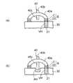
次いで、図5(a)に示すように、電極部品として可撓性電極端子40を用意する。可撓性電極端子40は上側にドーム状に膨らむ膨出部40a(本体部)とその上面中央部に設けられて上側に突き出る突出接続部40bとを備えている。 Next, as shown in FIG. 5A, a
可撓性電極端子40は圧力によって弾性変形する金属材料から形成される。これにより、可撓性電極端子40は、実装時に熱応力が発生する際にその応力を緩和できる程度に弾性変形して撓む。 The
そのような可撓性電極端子40として機能する金属材料としては、りん青銅、ベリリウム銅、又はチタン銅などのばね材料、あるいは、銅、ニッケルなどがある。可撓性電極端子40は、そのような金属板がプレス加工によって一体成形されて形成される。 Examples of the metal material that functions as the
可撓性電極端子40の突出接続部40bにインターポーザや半導体チップなどの他の電子部品が接続される。可撓性電極端子40はその本体部を膨出部40aとすることにより、下側、横方向又は斜め方向に容易に撓んで動くことができる。 Other electronic components such as an interposer and a semiconductor chip are connected to the protruding
さらに、膨出部40aの上に突出接続部40bが設けられているため、実装時の応力を突出接続部40bに集中させることができる。これにより、実装時の応力が突出接続部40bを介して膨出部40aに効率よく伝わり、膨出部40aが撓むことにより応力を容易に分散することができる。 Furthermore, since the protruding
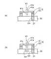
可撓性電極端子40の平面形状としては、図5(b)の例では、円形状の膨出部40aの上面中央部に突出接続部40bが設けられている。また、図5(b)に示すように、十字形状の膨出部40aの上面中央部に突出接続部40bが設けられていてもよい。さらには、図5(c)に示すように、横長長方形状(帯形状)の膨出部40aの上面中央部に突出接続部40bが設けられていてもよい。 As the planar shape of the
そして、図6に示すように、可撓性電極端子40の膨出部40aの終端部を図4(c)の構造体の接続電極Eに接続する。可撓性電極端子40はその下側に空間Sが設けられた状態で接続電極Eに接続される。 And as shown in FIG. 6, the terminal part of the bulging
可撓性電極端子40と接続電極Eとの接続方式としては、はんだ接続、金(Au)―金(Au)接続、金(Au)−錫(Su)接続、又は金(Au)−インジウム(In)接続などの金属接続、あるいは導電性ペーストによる接続がある。 As the connection method between the
可撓性電極端子40及び接続電極Eの各表面に上記した所要の組み合わせの金属層が形成されて各金属接続が行われる。例えば、可撓性電極端子40の外面全体に、最外層として金層やはんだ層などを形成して予め表面処理しておき、上記した金属接続を行ってもよい。あるいは、金/錫シートを介して可撓性電極端子40と接続電極Eとを金−錫接続してもよい。 The metal layers of the required combination described above are formed on the surfaces of the
以上により、第1実施形態の実装基板1(電子部品)が得られる。 As described above, the mounting substrate 1 (electronic component) of the first embodiment is obtained.
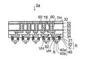
図6に示すように、第1実施形態の実装基板1では、ベース基板10にスルーホールTHが設けられており、スルーホールTH内に貫通電極TEが充填されている、ベース基板10の両面側には、貫通電極TEを介して相互接続される第1配線層20がそれぞれ形成されている。 As shown in FIG. 6, in the mounting
ベース基板10の上面側には、保護絶縁層30が形成されており、保護絶縁層30には第1配線層20に到達するビアホールVHが形成されている。ビアホールVH内には第1配線層20に接続されるビア導体21が充填されている。 A protective insulating
保護絶縁層30の上には、ビア導体21に接続される接続電極Eが形成されている。接続電極Eは導体パターン層22とその上のコンタクト層Cとにより形成される。 A connection electrode E connected to the via
また、ベース基板10の下面側には、第1配線層20の接続部上に開口部30xが設けられた保護絶縁層30が形成されている。第1配線層20の接続部にはコンタクト層Cが設けられている。 On the lower surface side of the
ベース基板10の上面側の接続電極Eには下側に空間Sが設けられた状態で可撓性電極端子40が接続されている。可撓性電極端子40は上側に膨らむ膨出部40a(本体部)とその上面中央部に設けられた突出接続部40bとを備えている。可撓性電極端子40の膨出部40aの下側が空間Sとなっており、圧力によって膨出部40aが空間S内で撓んで変形できるようになっている。 A
次に、図6の実装基板1に接続されるインターポーザ及び半導体チップについて説明する。 Next, an interposer and a semiconductor chip connected to the mounting
図7(a)に示すように、インターポーザ2では、シリコン基板50にスルーホールTHが形成されており、シリコン基板50の両面及びスルーホールTHの内面に絶縁層52が形成されている。そして、スルーホールTH内には貫通電極TEが充填されている。 As shown in FIG. 7A, in the
シリコン基板50の両面側には、貫通電極TEを介して相互接続される第1配線層60がそれぞれ形成されている。さらに、シリコン基板50の上面には、第1配線層60の接続部を露出させるようにして保護絶縁層34が形成されている。 On both sides of the
シリコン基板50の下面には第1配線層60を被覆する層間絶縁層32が形成されている。層間絶縁層32には第1配線層60に到達するビアホールVHが形成されている。さらに、層間絶縁層32の下面にはビアホールVHを介して第1配線層60に接続される第2配線層62が形成されている。 An interlayer insulating
層間絶縁層32の下面には、第2配線層62の接続部を露出させるようにして保護絶縁層34が形成されている。そして、第2配線層62の接続部に外部接続端子64が設けられている。 A protective insulating
このように、シリコン基板50の下面側の第1、第2配線層60,62によって、半導体チップに対応する上面側の第1配線層60の狭ピッチが実装基板1の接続電極Eの広ピッチに対応するようにピッチ変換される。例えば、シリコン基板50の上面側の第1配線層60のピッチは150μmであり、下面側の第2配線層62のピッチは300〜500μmに設定される。 As described above, the first and second wiring layers 60 and 62 on the lower surface side of the
なお、インターポーザ2の基板としてシリコン基板50を例示するが、シリコン基板50の代わりにガラス基板を使用してもよい。この場合は、絶縁層52が省略される。 In addition, although the
次いで、図7(b)に示すように、下面側にはんだバンプ72を備えた半導体チップ70(LSIチップ)を用意する。半導体チップ70はトランジスタなどの各種素子が形成されたシリコンウェハが切断されて得られる。 Next, as shown in FIG. 7B, a semiconductor chip 70 (LSI chip) having solder bumps 72 on the lower surface side is prepared. The
そして、図7(a)のインターポーザ2の上面側の第1配線層60の上にはんだを塗布し、半導体チップ70のはんだバンプ72をインターポーザ2の第1配線層60の上に配置する、さらに、加熱処理によってリフローはんだ付けを行う。このようにして、半導体チップ70がインターポーザ2にフリップチップ接続される。 Then, solder is applied on the
このとき、インターポーザ2(シリコン)と半導体チップ70(シリコン)とは熱膨張係数が同一であるため、熱応力の発生が抑制されて、接合部の信頼性が確保される。 At this time, since the thermal expansion coefficient is the same between the interposer 2 (silicon) and the semiconductor chip 70 (silicon), the generation of thermal stress is suppressed and the reliability of the joint portion is ensured.
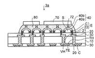
さらに、図8に示すように、半導体チップ70が実装されたインターポーザ2(図7(b))の下面の外部接続端子64(はんだ)を実装基板1(図6)の可撓性電極端子40の突出接続部40b上に配置し、加熱処理することによりリフローはんだ付けを行う。 Further, as shown in FIG. 8, the external connection terminal 64 (solder) on the lower surface of the interposer 2 (FIG. 7B) on which the
これにより、半導体チップ70がインターポーザ2を介して実装基板1に電気的に接続される。以上により、実施形態の半導体装置3が得られる。 As a result, the
このとき、実装時に加熱処理を行う際に、実装基板1(ガラスエポキシ樹脂)とインターポーザ2(シリコン)との間の熱膨張係数のミスマッチによって熱応力が発生する。しかしながら、本実施形態では、熱応力が発生するとしても、実装基板1の可撓性電極端子40が弾性変形して撓むことにより応力を分散することができる。 At this time, when heat treatment is performed at the time of mounting, thermal stress is generated due to a mismatch in the thermal expansion coefficient between the mounting substrate 1 (glass epoxy resin) and the interposer 2 (silicon). However, in this embodiment, even if thermal stress occurs, the stress can be dispersed by the
従って、実装基板1とインターポーザ2との接続部での残留応力の発生を低減することができる。これにより、実装基板1とインターポーザ2との接合部の破壊が回避され、半導体装置の信頼性を向上させることができる。 Therefore, it is possible to reduce the occurrence of residual stress at the connection portion between the mounting
錫(Sn)−銀(Ag)−銅(Cu)系などの鉛(Pb)フリーのはんだを使用する場合は、220〜250℃程度の比較的高い温度で加熱処理する必要がある。そのような場合であっても、本実施形態の可撓性電極端子40を備えた実装基板1を使用することにより、信頼性が高い半導体装置3を歩留りよく製造することができる。 When using lead (Pb) -free solder such as tin (Sn) -silver (Ag) -copper (Cu), it is necessary to heat-treat at a relatively high temperature of about 220 to 250 ° C. Even in such a case, by using the mounting
このように、本実施形態の応力緩和機能を有する可撓性電極端子40を備えた実装基板1を使用することにより、実装基板1とインターポーザ2との接合部に残留応力が集中することが回避され、半導体装置の電気接続の信頼性を向上させることができる。 As described above, by using the mounting
さらには、実装基板1とインターポーザ2との接合部に外部から機械的応力がかかるとしても、同様に可撓性電極端子40が撓むことにより応力を分散することができる。 Furthermore, even if mechanical stress is applied to the joint between the mounting
第1実施形態の半導体装置3は、可撓性電極端子40を備えた実装基板1を使用するため、半導体チップ70及びインターポーザ2の下側にアンダーフィル樹脂を充填しなくとも接合部の十分な信頼性を得ることができる。 Since the
図9に示すように、必要に応じて、半導体チップ70とインターポーザ2との間の隙間、及びインターポーザ2と実装基板1との間の隙間にアンダーフィル樹脂80を充填してもよい。接合部をアンダーフィル樹脂80で封止することにより、応力がさらに分散されるため、電気接続の信頼性をさらに向上させることができる。 As shown in FIG. 9, the
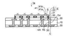
また、図10に示すように、図6の実装基板1の可撓性電極端子40の突出接続部40bに半導体チップ70のはんだバンプ72をフリップチップ接続することにより半導体装置3aとしてもよい。 As shown in FIG. 10, the
この場合も同様に、実装基板1(ガラスエポキシ樹脂)と半導体チップ70(シリコン)との間の熱膨張係数のミスマッチによって熱応力が発生するとしても、可撓性電極端子40が撓んで動くため、応力を分散することができる
これにより、実装基板1と半導体チップ70との接合部が破壊したり、半導体チップ70の素子が破壊するなどの不具合が解消され、半導体装置の電気接続の信頼性を向上させることができる。In this case as well, even if a thermal stress is generated due to a mismatch in thermal expansion coefficient between the mounting substrate 1 (glass epoxy resin) and the semiconductor chip 70 (silicon), the
この場合も、図11に示すように、半導体チップ70と実装基板1との間の隙間にアンダーフィル樹脂80を充填してもよい。 Also in this case, as shown in FIG. 11, the
なお、図9及び図11において、可撓性電極端子40と下側の基板との間の空間Sにアンダーフィル樹脂80を充填してもよい。 9 and 11, the
前述した説明では、実装基板1に可撓性電極端子40を設ける形態を説明した。他の形態として、図12に示すように、図7(a)のインターポーザ2の外部接続端子64の代わりに、可撓性電極端子40を設けてもよい。 In the above description, the embodiment in which the
つまり、図12に示すインターポーザ2aでは、図7(a)のインターポーザ2と同一の下面側の保護絶縁層34に第2配線層62に到達するビアホールVHが形成されている。また、ビアホールVHにビア導体21が充填されている。 That is, in the
さらに、保護絶縁層34の下面に、ビア導体21に接続されて導体パターン層22及びコンタクト層から形成された接続電極Eが設けられている。そして、接続電極Eに可撓性電極端子40が同様に接続されている。 Furthermore, a connection electrode E is provided on the lower surface of the protective insulating
図12に示すインターポーザ2aを製造する際は、シリコンウェハの状態で各工程が遂行された後に、シリコンウェハが切断されて個々のインターポーザ2aが得られる。 When manufacturing the
このようにして、図6の実装基板1と同様な可撓性電極端子40がインターポーザ2aに設けられる。図12のインターポーザ2aの上面側の第1配線層60に可撓性電極端子40を設けてもよい。 Thus, the
図12の可撓性電極端子40を備えたインターポーザ2aを実装基板1に接続する場合は、必ずしも実装基板1に可撓性電極端子40が設けられている必要はない。つまり、実装基板1にインターポーザ2aを接続する場合は、実装基板1及びインターポーザ2aの少なくとも一方に設けられた可撓性電極端子40を介して接続されていればよい。 When connecting the
また、図13に示すように、実装基板やインターポーザなどの配線基板系の電子部品の他に、半導体チップ70に同様な可撓性電極端子40を設けてもよい。 Further, as shown in FIG. 13, a
つまり、図13に示す半導体チップ70では、接続パッド74の上にビアホールVHが設けられた保護絶縁層76が形成されている。また、ビアホールVH内に接続パッド74に接続されるビア導体21が形成されている。 That is, in the
さらに、保護絶縁層76の下面に、ビア導体21に接続されて導体パターン層22及びコンタクト層Cから形成される接続電極Eが設けられている。そして、接続電極Eに可撓性電極端子40が同様に接続されている。 Further, a connection electrode E formed from the
図13に示す半導体チップ70を製造する際は、シリコンウェハの状態で各工程が遂行された後に、シリコンウェハが切断されて個々の半導体チップ70が得られる。 When manufacturing the
このようにして、図6の実装基板1と同様な可撓性電極端子40が半導体チップ70に設けられている。半導体チップ70を例示したが、キャパシタ、抵抗素子、インダクタなどの各種の電子部品に外部接続端子として可撓性電極端子40を設けてもよい。 In this way, the
そして、半導体チップ70の可撓性電極端子40がインターポーザや実装基板に接続される。この場合も、半導体チップ70とインターポーザ(又は実装基板)との少なくとも一方に設けられた可撓性電極端子40を介して接続されていればよい。 And the
図14(a)及び(b)には、第1実施形態の変形例の可撓性電極端子が示されている。図14(a)に示すように、可撓性電極端子40の下面中央部に下側突出部40cがさらに設けられていてもよい。 FIGS. 14A and 14B show a flexible electrode terminal according to a modification of the first embodiment. As shown in FIG. 14A, a
可撓性電極端子40の下側突出部40cは、可撓性電極端子40が上側から下側に押圧されて動く際に、下側突出部40cの先端が保護絶縁層30に当たって動きを止めるストッパとして機能する。 The lower protruding
また、図14(b)に示すように、保護絶縁層30に可撓性電極端子40の下側突出部40cに対応する位置決めホールAHを形成し、可撓性電極端子40の下側突出部40cが位置決めホールAHに挿入されるようにしてもよい。接続電極Eは実装基板又はインターポーザの上に形成されており、実装基板又はインターポーザ(保護絶縁層30)に位置決めホールAHが設けられる。 14B, a positioning hole AH corresponding to the lower protruding
この場合は、下側突出部40cは位置決めホールAHに挿入されるように膨出部40aの終端より下側に延びて形成される。 In this case, the
可撓性電極端子40を接続電極Eに配置する際に、保護絶縁層30の位置決めホールAHに可撓性電極端子40の下側突出部40cを挿入させることにより、容易に位置決めすることができる。特に治具を使用して可撓性電極端子40を振り込む際に、可撓性電極端子40を接続電極Eの上に高精度で効率よく配置することができる。 When the
(第2の実施の形態)
図15は第2実施形態の実装基板(電子部品)を示す断面図、図16は同じくインターポーザ(電子部品)を示す断面図、図17は同じく半導体チップ(電子部品)を示す断面図である。第2実施形態の特徴は可撓性電極端子の本体部が平板部からなることにあり、その他の要素は第1実施形態と同一であるのでその詳しい説明を省略する。(Second Embodiment)
15 is a cross-sectional view showing a mounting substrate (electronic component) according to the second embodiment, FIG. 16 is a cross-sectional view showing the same interposer (electronic component), and FIG. 17 is a cross-sectional view showing the same semiconductor chip (electronic component). The feature of the second embodiment is that the main body portion of the flexible electrode terminal is a flat plate portion, and the other elements are the same as those of the first embodiment, and therefore detailed description thereof is omitted.
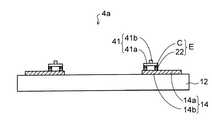
図15に示すように、第2実施形態の実装基板1aに設けられた可撓性電極端子41は、平板部41a(本体部)とその上面中央部に設けられた突出接続部41bとを備える。可撓性電極端子41の金属材料は、第1実施形態と同一のものが使用される。 As shown in FIG. 15, the
可撓性電極端子41の平板部41aの端部が接続電極Eに接続される。可撓性電極端子41の平板部41aは上側に膨出していないので、その下に空間Sを十分に確保するために接続電極Eの高さが第1実施形態より高く設定される。接続電極Eの高さは、例えは20〜50μm程度である。 An end portion of the
第2実施形態に係る可撓性電極端子41では、第1実施形態と同様に、平板部41aの上側中央部に突出接続部41bが設けられているので、応力を突出接続部41bに集中させることができる。これにより、応力が突出接続部41bを介して平板部41aに効率よく伝わり、平板部41aが弾性変形して撓むことにより応力を容易に分散することができる。 In the
図16に示すように、第1実施形態の図12と同様に、インターポーザ2b(電子部品)の接続電極Eに平板部41aを備えた可撓性電極端子41を接続してもよい。 As shown in FIG. 16, similarly to FIG. 12 of the first embodiment, a
あるいは、図17に示すように、第1実施形態の図13と同様に、半導体チップ70(電子部品)の接続電極Eに平板部41aを備えた可撓性電極端子41を接続してもよい。 Alternatively, as shown in FIG. 17, the
図18には、第2実施形態の変形例の可撓性電極端子が示されている。図18(a)に示すように、第1実施形態の図14(a)と同様に、可撓性電極端子41の下面中央部に下側突出部41cがさらに設けられていてもよい。 FIG. 18 shows a flexible electrode terminal according to a modification of the second embodiment. As shown in FIG. 18A, similarly to FIG. 14A of the first embodiment, a
第1実施形態と同様に、可撓性電極端子41の下側突出部41cは、可撓性電極端子41が上側から下側に押圧されて動く際に動きを止めるストッパとして機能する。 Similar to the first embodiment, the lower protruding
また、図18(b)に示すように、第1実施形態の図14(b)と同様に、保護絶縁層30に可撓性電極端子41の下側突出部41cに対応する位置決めホールAHを形成し、可撓性電極端子41の下側突出部41cが位置決めホールAHに挿入されるようにしてもよい。第1実施形態と同様に、保護絶縁層30の位置決めホールAHに可撓性電極端子41の下側突出部41cを挿入させることにより、容易に位置決めすることができる。 Further, as shown in FIG. 18B, as in FIG. 14B of the first embodiment, a positioning hole AH corresponding to the lower protruding
接続電極Eは実装基板又はインターポーザの上に形成されており、実装基板又はインターポーザ(保護絶縁層30)に位置決めホールAHが設けられる。 The connection electrode E is formed on the mounting substrate or the interposer, and the positioning hole AH is provided in the mounting substrate or the interposer (protective insulating layer 30).
第2実施形態においても、第1実施形態の図8と同様に、実装基板1aの可撓性電極端子41に、半導体チップ70がフリップチップ接続されたインターポーザ2の外部接続端子64が接続される。 Also in the second embodiment, as in FIG. 8 of the first embodiment, the
あるいは、第1実施形態の図10のように、実装基板1aの可撓性電極端子41に半導体チップ70のはんだバンプ72が接続される。又は、可撓性電極端子41を備えたインターポーザ2aや半導体チップ70を実装基板に接続してもよい。 Alternatively, as shown in FIG. 10 of the first embodiment, the solder bumps 72 of the
第2実施形態の可撓性電極端子41を備える実装基板1a、インターポーザ2b又は半導体チップ70は第1実施形態と同様な効果を奏する。 The mounting
(第3の実施の形態)
図19(a)及び(b)は第3実施形態のプローブ基板(電子部品)を示す図、図20は図19(b)のプローブ基板に被試験対象物が配置された様子を示す断面図である。(Third embodiment)
FIGS. 19A and 19B are diagrams showing a probe board (electronic component) according to the third embodiment, and FIG. 20 is a cross-sectional view showing a state in which an object to be tested is arranged on the probe board of FIG. It is.
第3実施形態では、可撓性電極端子をプローブ基板に適用する形態について説明する。その他の要素は第1、第2実施形態と同一であるのでその詳しい説明を省略する。 3rd Embodiment demonstrates the form which applies a flexible electrode terminal to a probe board | substrate. Since other elements are the same as those in the first and second embodiments, detailed description thereof will be omitted.
図19(a)の平面図に示すように、第3実施形態のプローブ基板4では、絶縁基板12の上に、周縁側から内側に延在する複数の配線パターン14がくし歯状に並んで形成されている。各配線パターン14は周縁側に配置された接続パッド14bとそこから内側に延在する延在部14bとを備えている。絶縁基板12の代わりに、外面が絶縁層で被覆されたシリコンなどの半導体基板を使用してもよい。 As shown in the plan view of FIG. 19A, in the
さらに、図19(b)の断面図を加えて参照すると、配線パターン14の延在部14bの先端部に導体パターン層22及びコンタクト層Cから形成された接続電極Eが設けられている。 Furthermore, referring to FIG. 19B in addition to the cross-sectional view, a connection electrode E formed of the
また、第1実施形態と同様に、配線パターン14の接続電極Eには下側に空間Sが設けられた状態で可撓性電極端子40が接続されている。可撓性電極端子40は上側に膨らむ膨出部40a(本体部)とその上面中央部に設けられた突出接続部40bとを備えている。このようにして、可撓性電極端子40は絶縁基板12上のリング状の領域に配列されている。 Similarly to the first embodiment, the
第3実施形態では、プローブ基板4に可撓性電極端子40が設けられており、第1実施形態と同様に、可撓性電極端子40を下側に押圧することによって膨出部40aが空間S内で撓んで変形できるようになっている。 In the third embodiment, the
なお、絶縁基板12の両面側に配線パターン14が形成され、絶縁基板12に設けられた貫通電極を介して両面側の配線パターンが相互接続されていてもよい。 In addition, the
第3実施形態のプローブ基板4の可撓性電極端子40は、被試験対象物の電極パッドに適応するように配列されている。そして、図20に示すように、プローブ基板4の可撓性電極端子40の上に被検査対象物90の電極パッド92が配置される。 The
このとき、被検査対象物90を下側に押圧した状態で治具(不図示)によって固定すると、可撓性電極端子40が撓んで変形する。これにより、被検査対象物90の電極パッド92が所要のコンタクト荷重でプローブ基板4の可撓性電極端子40に押圧されて導通可能な状態となる。 At this time, if the
プローブ基板4の配線パターン14の接続パッド14aには検査用装置の端子(不図示)が電気的に接続され、検査用装置からプローブ基板4を介して被検査対象物90に各種の試験信号が供給されて被検査対象物90の電気特性が測定される。 A terminal (not shown) of an inspection device is electrically connected to the
プローブ基板4の接続端子として撓んで変形する可撓性電極端子40を使用することにより、被検査対象物90の全ての電極パッド92をプローブ基板4の可撓性電極端子40に確実に導通させることができる。これにより、被検査対象物90の電気測定を行う際の信頼性を確保することができる。 By using the
被検査対象物90としては、半導体素子(LSIチップ)、所要の素子が形成された半導体ウェハ、CSP(Chip Size Package)、又は配線基板などがあり、プローブ基板4を使用して各種の電子装置の電気特性を測定することができる。 The
なお、電極パッド92が周辺に配置されたペリフェラル型の被検査対象物90に対応するプローブ基板4を例示したが、電極パッドが基板全体に格子状に配置されるエリアアレイ型の被検査対象物に対応するように可撓性電極端子40を配列してもよい。 The
また、図21に示すプローブ基板4aのように、第2実施形態の図15などと同様に、平板部41a(本体部)とその上面中央部に設けられた突出接続部41とを備えた可撓性接続端子41を使用してもよい。 Further, like the
また、図22(a)に示す変形例のように、第1実施形態の図14(a)と同様に、図19(b)の可撓性接続端子40の下面中央部に下側突出部40cを設けてもよい。 Further, as in the modification shown in FIG. 22A, as in FIG. 14A of the first embodiment, a lower protruding portion is formed at the center of the lower surface of the
さらには、図22(b)に示すように、第1実施形態の図14(b)と同様に、配線パターン14に位置決めホールAHを形成し、可撓性接続端子40の下側突出部40cが位置決めホールAHに挿入されるようにしてもよい。 Furthermore, as shown in FIG. 22B, the positioning hole AH is formed in the
また、図23(a)に別の変形例に示すように、第2実施形態の図18(a)と同様に、図21の可撓性接続端子41の下面中央部に下側突出部41cを設けてもよい。 Further, as shown in FIG. 23A as another modification, the
さらには、図23(b)に示すように、第2実施形態の図18(b)と同様に、配線パターン14に位置決めホールAHを形成し、可撓性接続端子41の下側突出部41cが位置決めホールAHに挿入されるようにしてもよい。 Further, as shown in FIG. 23B, as in FIG. 18B of the second embodiment, a positioning hole AH is formed in the
第3実施形態では、可撓性電極端子を備えた電子部品としてプローブ基板4を例示しており、第1、第2実施形態と同様な効果を奏する。 In 3rd Embodiment, the probe board |
1,1a…実装基板(電子部品)、2,2a、2b…インターポーザ(電子部品)、3,3a…半導体装置、4,4a…プローブ基板、10…ベース基板、20…第1配線層、21…ビア導体、22…導体パターン層、30,34,76…保護絶縁層、30x…開口部、32…層間絶縁層、40,41…可撓性電極端子、40a…膨出部(本体部)、41a…平板部(本体部)、40b,41b…突出接続部、40c,41c…下側突出部、50…シリコン基板、52…絶縁層、60…第1配線層、62…第2配線層、64…外部接続端子、70…半導体チップ(電子部品)、72…はんだバンプ、80…アンダーフィル樹脂、90…被検査対象物、92…電極パッド、AH…位置決めホール、C…コンタクト層、E…接続電極、S…空間、TE…貫通電極、TH…スルーホール、VH…ビアホール。DESCRIPTION OF
Claims (10)
Translated fromJapanese下側に空間が設けられた状態で前記接続電極に接続され、本体部と、前記本体部の上面に設けられた突出接続部とを備え、圧力によって弾性変形する可撓性電極端子とを有することを特徴とする電子部品。A connection electrode;
Connected to the connection electrode in a state where a space is provided on the lower side, and includes a main body portion and a projecting connection portion provided on the upper surface of the main body portion, and a flexible electrode terminal that is elastically deformed by pressure. An electronic component characterized by that.
Priority Applications (1)
| Application Number | Priority Date | Filing Date | Title |
|---|---|---|---|
| JP2012088045AJP2013030748A (en) | 2011-06-21 | 2012-04-09 | Electronic component |
Applications Claiming Priority (3)
| Application Number | Priority Date | Filing Date | Title |
|---|---|---|---|
| JP2011136971 | 2011-06-21 | ||
| JP2011136971 | 2011-06-21 | ||
| JP2012088045AJP2013030748A (en) | 2011-06-21 | 2012-04-09 | Electronic component |
Publications (1)
| Publication Number | Publication Date |
|---|---|
| JP2013030748Atrue JP2013030748A (en) | 2013-02-07 |
Family
ID=47361649
Family Applications (1)
| Application Number | Title | Priority Date | Filing Date |
|---|---|---|---|
| JP2012088045APendingJP2013030748A (en) | 2011-06-21 | 2012-04-09 | Electronic component |
Country Status (2)
| Country | Link |
|---|---|
| US (1) | US20120327574A1 (en) |
| JP (1) | JP2013030748A (en) |
Cited By (3)
| Publication number | Priority date | Publication date | Assignee | Title |
|---|---|---|---|---|
| CN106067455A (en)* | 2015-04-23 | 2016-11-02 | 爱思开海力士有限公司 | Semiconductor package with interconnect components |
| JP2017113077A (en)* | 2015-12-21 | 2017-06-29 | ソニー・オリンパスメディカルソリューションズ株式会社 | Endoscopic device |
| JP2021044441A (en)* | 2019-09-12 | 2021-03-18 | キオクシア株式会社 | Semiconductor device and manufacturing method thereof |
Families Citing this family (2)
| Publication number | Priority date | Publication date | Assignee | Title |
|---|---|---|---|---|
| US9385098B2 (en)* | 2012-11-21 | 2016-07-05 | Nvidia Corporation | Variable-size solder bump structures for integrated circuit packaging |
| TWI554174B (en)* | 2014-11-04 | 2016-10-11 | 上海兆芯集成電路有限公司 | Circuit substrate and semiconductor substrate |
Family Cites Families (2)
| Publication number | Priority date | Publication date | Assignee | Title |
|---|---|---|---|---|
| US5228861A (en)* | 1992-06-12 | 1993-07-20 | Amp Incorporated | High density electrical connector system |
| US5518964A (en)* | 1994-07-07 | 1996-05-21 | Tessera, Inc. | Microelectronic mounting with multiple lead deformation and bonding |
- 2012
- 2012-04-09JPJP2012088045Apatent/JP2013030748A/enactivePending
- 2012-06-20USUS13/528,074patent/US20120327574A1/ennot_activeAbandoned
Cited By (7)
| Publication number | Priority date | Publication date | Assignee | Title |
|---|---|---|---|---|
| CN106067455A (en)* | 2015-04-23 | 2016-11-02 | 爱思开海力士有限公司 | Semiconductor package with interconnect components |
| CN106067455B (en)* | 2015-04-23 | 2019-11-19 | 爱思开海力士有限公司 | Semiconductor package with interconnect components |
| JP2017113077A (en)* | 2015-12-21 | 2017-06-29 | ソニー・オリンパスメディカルソリューションズ株式会社 | Endoscopic device |
| US10561306B2 (en) | 2015-12-21 | 2020-02-18 | Sony Olympus Medical Solutions Inc. | Endoscopic device |
| US11122969B2 (en) | 2015-12-21 | 2021-09-21 | Sony Olympus Medical Solutions Inc. | Endoscopic device |
| JP2021044441A (en)* | 2019-09-12 | 2021-03-18 | キオクシア株式会社 | Semiconductor device and manufacturing method thereof |
| JP7293056B2 (en) | 2019-09-12 | 2023-06-19 | キオクシア株式会社 | Semiconductor device and its manufacturing method |
Also Published As
| Publication number | Publication date |
|---|---|
| US20120327574A1 (en) | 2012-12-27 |
Similar Documents
| Publication | Publication Date | Title |
|---|---|---|
| US9530744B2 (en) | Semiconductor device and method of manufacturing the same | |
| JP5808586B2 (en) | Manufacturing method of interposer | |
| JP5500870B2 (en) | Substrate with connection terminal and socket for electronic parts | |
| TWI395274B (en) | Method of manufacturing a circuit substrate and method of manufacturing an electronic parts packaging structure | |
| US6816385B1 (en) | Compliant laminate connector | |
| US8450853B2 (en) | Semiconductor device and a method of manufacturing the same, and an electronic device | |
| JP5582995B2 (en) | socket | |
| JP5788166B2 (en) | Connection terminal structure, manufacturing method thereof, and socket | |
| JPWO2007072616A1 (en) | Component built-in module and manufacturing method thereof | |
| JP6064705B2 (en) | Semiconductor device manufacturing method and semiconductor mounting substrate | |
| JP2010232333A (en) | Semiconductor device, method of manufacturing the same, and electronic device | |
| US10129980B2 (en) | Circuit board and electronic component device | |
| JP4550102B2 (en) | Semiconductor package, manufacturing method thereof, and semiconductor device including semiconductor package | |
| JP2013030748A (en) | Electronic component | |
| KR20250079113A (en) | Semiconductor device and manufacturing method thereof | |
| JP4932744B2 (en) | WIRING BOARD AND ITS MANUFACTURING METHOD, ELECTRONIC COMPONENT DEVICE AND ITS MANUFACTURING METHOD | |
| US9024439B2 (en) | Substrates having bumps with holes, semiconductor chips having bumps with holes, semiconductor packages formed using the same, and methods of fabricating the same | |
| CN107305849B (en) | Packaging structure and manufacturing method thereof | |
| JP2001168224A (en) | Semiconductor device, electronic circuit device, and its manufacturing method | |
| US20220293748A1 (en) | Method for Manufacturing Semiconductor Device and Semiconductor Device | |
| KR101148494B1 (en) | A semiconductor device comprsing a connecting metal layer and a method of manufacturing the same | |
| JP2007158024A (en) | Bga-type semiconductor device and its manufacturing method | |
| JP2007294526A (en) | Semiconductor device, semiconductor device, and mounting substrate | |
| TWI575619B (en) | Semiconductor package structure and manufacturing method thereof | |
| JP2014127696A (en) | Semiconductor element mounting printed wiring board |