JP2012523623A - Partitioning flash memory data storage devices - Google Patents
Partitioning flash memory data storage devicesDownload PDFInfo
- Publication number
- JP2012523623A JP2012523623AJP2012504741AJP2012504741AJP2012523623AJP 2012523623 AJP2012523623 AJP 2012523623AJP 2012504741 AJP2012504741 AJP 2012504741AJP 2012504741 AJP2012504741 AJP 2012504741AJP 2012523623 AJP2012523623 AJP 2012523623A
- Authority
- JP
- Japan
- Prior art keywords
- subset
- memory chips
- storage device
- data storage
- partition
- Prior art date
- Legal status (The legal status is an assumption and is not a legal conclusion. Google has not performed a legal analysis and makes no representation as to the accuracy of the status listed.)
- Pending
Links
Images


Classifications
- G—PHYSICS
- G06—COMPUTING OR CALCULATING; COUNTING
- G06F—ELECTRIC DIGITAL DATA PROCESSING
- G06F3/00—Input arrangements for transferring data to be processed into a form capable of being handled by the computer; Output arrangements for transferring data from processing unit to output unit, e.g. interface arrangements
- G06F3/06—Digital input from, or digital output to, record carriers, e.g. RAID, emulated record carriers or networked record carriers
- G06F3/0601—Interfaces specially adapted for storage systems
- G06F3/0668—Interfaces specially adapted for storage systems adopting a particular infrastructure
- G06F3/0671—In-line storage system
- G06F3/0673—Single storage device
- G06F3/0679—Non-volatile semiconductor memory device, e.g. flash memory, one time programmable memory [OTP]
- G—PHYSICS
- G06—COMPUTING OR CALCULATING; COUNTING
- G06F—ELECTRIC DIGITAL DATA PROCESSING
- G06F12/00—Accessing, addressing or allocating within memory systems or architectures
- G06F12/02—Addressing or allocation; Relocation
- G06F12/0223—User address space allocation, e.g. contiguous or non contiguous base addressing
- G06F12/023—Free address space management
- G06F12/0238—Memory management in non-volatile memory, e.g. resistive RAM or ferroelectric memory
- G06F12/0246—Memory management in non-volatile memory, e.g. resistive RAM or ferroelectric memory in block erasable memory, e.g. flash memory
- G—PHYSICS
- G06—COMPUTING OR CALCULATING; COUNTING
- G06F—ELECTRIC DIGITAL DATA PROCESSING
- G06F3/00—Input arrangements for transferring data to be processed into a form capable of being handled by the computer; Output arrangements for transferring data from processing unit to output unit, e.g. interface arrangements
- G06F3/06—Digital input from, or digital output to, record carriers, e.g. RAID, emulated record carriers or networked record carriers
- G06F3/0601—Interfaces specially adapted for storage systems
- G06F3/0602—Interfaces specially adapted for storage systems specifically adapted to achieve a particular effect
- G06F3/061—Improving I/O performance
- G06F3/0613—Improving I/O performance in relation to throughput
- G—PHYSICS
- G06—COMPUTING OR CALCULATING; COUNTING
- G06F—ELECTRIC DIGITAL DATA PROCESSING
- G06F3/00—Input arrangements for transferring data to be processed into a form capable of being handled by the computer; Output arrangements for transferring data from processing unit to output unit, e.g. interface arrangements
- G06F3/06—Digital input from, or digital output to, record carriers, e.g. RAID, emulated record carriers or networked record carriers
- G06F3/0601—Interfaces specially adapted for storage systems
- G06F3/0602—Interfaces specially adapted for storage systems specifically adapted to achieve a particular effect
- G06F3/0614—Improving the reliability of storage systems
- G06F3/0619—Improving the reliability of storage systems in relation to data integrity, e.g. data losses, bit errors
- G—PHYSICS
- G06—COMPUTING OR CALCULATING; COUNTING
- G06F—ELECTRIC DIGITAL DATA PROCESSING
- G06F3/00—Input arrangements for transferring data to be processed into a form capable of being handled by the computer; Output arrangements for transferring data from processing unit to output unit, e.g. interface arrangements
- G06F3/06—Digital input from, or digital output to, record carriers, e.g. RAID, emulated record carriers or networked record carriers
- G06F3/0601—Interfaces specially adapted for storage systems
- G06F3/0628—Interfaces specially adapted for storage systems making use of a particular technique
- G06F3/0638—Organizing or formatting or addressing of data
- G06F3/0644—Management of space entities, e.g. partitions, extents, pools
- G—PHYSICS
- G06—COMPUTING OR CALCULATING; COUNTING
- G06F—ELECTRIC DIGITAL DATA PROCESSING
- G06F3/00—Input arrangements for transferring data to be processed into a form capable of being handled by the computer; Output arrangements for transferring data from processing unit to output unit, e.g. interface arrangements
- G06F3/06—Digital input from, or digital output to, record carriers, e.g. RAID, emulated record carriers or networked record carriers
- G06F3/0601—Interfaces specially adapted for storage systems
- G06F3/0628—Interfaces specially adapted for storage systems making use of a particular technique
- G06F3/0655—Vertical data movement, i.e. input-output transfer; data movement between one or more hosts and one or more storage devices
- G06F3/0659—Command handling arrangements, e.g. command buffers, queues, command scheduling
Landscapes
- Engineering & Computer Science (AREA)
- Theoretical Computer Science (AREA)
- Physics & Mathematics (AREA)
- General Engineering & Computer Science (AREA)
- General Physics & Mathematics (AREA)
- Human Computer Interaction (AREA)
- Computer Security & Cryptography (AREA)
- Techniques For Improving Reliability Of Storages (AREA)
- Bus Control (AREA)
- Information Retrieval, Db Structures And Fs Structures Therefor (AREA)
- Information Transfer Systems (AREA)
- Image Processing (AREA)
- Memory System Of A Hierarchy Structure (AREA)
Abstract
Translated fromJapaneseDescription
Translated fromJapanese(関連出願の相互参照)
本出願は、引用により全体として本明細書中に組み込まれている、2009年4月8日に出願された「データストレージデバイス(DATA STORAGE DEVICE)」と題する米国仮出願第61/167,709号、及び2009年6月17日に出願された「フラッシュメモリデータストレージデバイスにおけるパーティショニング及びストライピング(PARTITIONING AND STRIPING IN A FLASH MEMORY DATA STORAGE DEVICE)」と題する米国仮出願第61/187,835号の利益を主張するものである。(Cross-reference of related applications)
This application is a US Provisional Application No. 61 / 167,709 entitled “DATA STORAGE DEVICE,” filed April 8, 2009, which is incorporated herein by reference in its entirety. Claims the benefit of US Provisional Application No. 61 / 187,835, filed June 17, 2009, entitled "PARTITIONING AND STRIPING IN A FLASH MEMORY DATA STORAGE DEVICE" It is.
(技術分野)
この説明は、データストレージデバイスに関する。(Technical field)
This description relates to data storage devices.
(背景)
データストレージデバイスは、データを格納するために使用することができる。データストレージデバイスは、コンピューティングデバイスのデータストレージの必要性に備えるためにコンピューティングデバイスと共に使用することができる。場合によっては、膨大量のデータをデータストレージデバイスに格納することが望ましいこともある。また、データストレージデバイスとの間でデータの迅速な読み取り及び書き込みを行うためのコマンドを実行することが望ましい場合もある。(background)
A data storage device can be used to store data. The data storage device can be used with a computing device to prepare for the data storage needs of the computing device. In some cases, it may be desirable to store a large amount of data in a data storage device. In addition, it may be desirable to execute commands to quickly read and write data to and from the data storage device.
(要旨)
第1の一般的な態様によれば、複数のメモリチップを含むデータストレージデバイスをパーティション化する方法が開示される。方法は、データストレージデバイス内のメモリチップの数を決定することを含む。データストレージデバイスに結合されたホストは、データストレージデバイスの第1のパーティション及び第2を定義し、第1のパーティションは複数のメモリチップの第1のサブセットを含み、第2のパーティションは複数のメモリチップの第2のサブセットを含む。第1のサブセットは、第2のサブセットのメモリチップを含むことはなく、第2のサブセットは、第1のサブセットのメモリチップを含むことはない。(Summary)
According to a first general aspect, a method for partitioning a data storage device including a plurality of memory chips is disclosed. The method includes determining the number of memory chips in the data storage device. A host coupled to the data storage device defines a first partition and a second of the data storage device, the first partition includes a first subset of the plurality of memory chips, and the second partition includes the plurality of memories Includes a second subset of chips. The first subset does not include the second subset of memory chips, and the second subset does not include the first subset of memory chips.
もう1つの一般的な態様において、複数のメモリチップを含むデータストレージデバイスをパーティション化する方法が開示され、そこでデータストレージデバイス内のメモリチップの数を含むデータストレージデバイスの物理構成、及びデータストレージデバイスのパーティション化方式が読み取られる。データストレージデバイスに結合されたホストは、データストレージデバイスの第1のパーティション及び第2のパーティションを定義し、第1のパーティションは複数のメモリチップの第1のサブセットを含み、第2のパーティションは複数のメモリチップの第2のサブセットを含み、第1のサブセットは、第2のサブセットのメモリチップを含むことはなく、第2のサブセットは、第1のサブセットのメモリチップを含むことはない。論理メモリから物理メモリへのマップは第1のパーティションに割り振られ、論理メモリから物理メモリへのマップは第1のパーティションに割り振られる。 In another general aspect, a method for partitioning a data storage device including a plurality of memory chips is disclosed, wherein the physical configuration of the data storage device includes the number of memory chips in the data storage device, and the data storage device The partitioning scheme is read. A host coupled to the data storage device defines a first partition and a second partition of the data storage device, the first partition includes a first subset of the plurality of memory chips, and the second partition includes a plurality of second partitions. The first subset does not include the second subset of memory chips, and the second subset does not include the first subset of memory chips. A map from logical memory to physical memory is allocated to the first partition, and a map from logical memory to physical memory is allocated to the first partition.
実施態様は、1つ以上の以下の特徴を含むことができる。データは、第2のパーティションからのデータの読み取り中に、第1のパーティションに書き込むことができる。データストレージデバイス内のメモリチップの数を決定することは、データストレージデバイス内のメモリチップの数を指示する情報をデータストレージデバイスからホストに送信することを含むことができる。ホストは、ホストからデータを書き込むデータストレージデバイス内のアドレス位置を定義することができ、アドレス位置は、データが複数のメモリチップのうちの特定の1つに書き込まれることを指定する。 Implementations can include one or more of the following features. Data can be written to the first partition while reading data from the second partition. Determining the number of memory chips in the data storage device can include transmitting information indicating the number of memory chips in the data storage device from the data storage device to the host. The host can define an address location in the data storage device to write data from the host, and the address location specifies that the data is written to a particular one of the plurality of memory chips.
データストレージデバイスは、ホストと複数のメモリチップ間のデータの通信のための複数の物理チャネルを含むことができ、各チャネルは異なる複数のメモリチップに機能的に接続され、次いで、物理チャネルの数が決定されてもよい。チャネルの第1のサブセット及び第2のサブセットが定義されてもよく、チャネルの第1のサブセットのチャネルは、メモリチップの第1のサブセットのメモリチップのみに機能的に接続され、チャネルの第2のサブセットのチャネルは、メモリチップの第2のサブセットのメモリチップのみに機能的に接続される。ホストは、ホストからデータを書き込むデータストレージデバイス内のアドレス位置を定義することができ、アドレス位置は、特定のチャネルを通じてデータが複数のメモリチップのうちの特定の1つに書き込まれることを指定する。第1のパーティションは、単一のチャネルに機能的に接続されるメモリチップを含むことができる。 A data storage device can include multiple physical channels for communication of data between a host and multiple memory chips, each channel functionally connected to a different multiple memory chip, and then the number of physical channels May be determined. A first subset and a second subset of channels may be defined, and the channels of the first subset of channels are functionally connected only to the memory chips of the first subset of memory chips and the second subset of channels The subset of channels are functionally connected only to the memory chips of the second subset of memory chips. The host can define an address location in the data storage device that writes data from the host, and the address location specifies that data is written to a specific one of the multiple memory chips through a specific channel. . The first partition can include a memory chip that is functionally connected to a single channel.
ホストは、複数のメモリチップの第3のサブセットを含むようにデータストレージデバイスの第1のパーティションを再定義することができ、第3のサブセットは第1のサブセットとは異なり、第3のサブセットは第2のサブセットのメモリチップを含むことはなく、第2のサブセットは第3のサブセットのメモリチップを含むことはない。第1のサブセットのメモリチップの1つに障害が生じたか又は障害発生に近づきつつあることを示す指示が受信されてもよく、次いで、第1のパーティションを再定義することは、障害が生じたか又は障害発生に近づきつつあるメモリチップを除いた第3のサブセットをメモリチップの第1のサブセットとして定義することを含むことができる。 The host can redefine the first partition of the data storage device to include a third subset of the plurality of memory chips, where the third subset is different from the first subset and the third subset is The second subset of memory chips is not included, and the second subset does not include the third subset of memory chips. An indication may be received indicating that one of the first subset of memory chips has failed or is approaching the failure, and then redefining the first partition has failed Alternatively, defining a third subset, excluding memory chips approaching failure, as the first subset of memory chips may be included.
もう1つの一般的な態様において、装置は、複数のメモリチップを含むデータストレージデバイスと、インターフェイスを介してデータストレージデバイスに機能的に結合されたホストとを含む。ホストは、データストレージデバイス内のメモリチップの数を検出するように構成された構成検出エンジン、及びパーティションエンジンを含む。パーティションエンジンは、データストレージデバイスの第1のパーティション及びデータストレージデバイスの第2のパーティションを定義するように構成され、第1のパーティションは複数のメモリチップの第1のサブセットを含み、第2のパーティションは複数のメモリチップの第2のサブセットを含み、第1のサブセットは、第2のサブセットのメモリチップを含むことはなく、第2のサブセットは、第1のサブセットのメモリチップを含むことはない。 In another general aspect, an apparatus includes a data storage device that includes a plurality of memory chips and a host that is functionally coupled to the data storage device via an interface. The host includes a configuration engine and a partition engine configured to detect the number of memory chips in the data storage device. The partition engine is configured to define a first partition of the data storage device and a second partition of the data storage device, the first partition including a first subset of the plurality of memory chips, and the second partition Includes a second subset of the plurality of memory chips, the first subset does not include the second subset of memory chips, and the second subset does not include the first subset of memory chips .
もう1つの一般的な態様において、装置は、複数のメモリチップを含むデータストレージデバイスと、インターフェイスを介してデータストレージデバイスに機能的に結合されたホストとを含む。ホストは、データストレージデバイス内のメモリチップの数を含むデータストレージデバイスの物理構成を読み取るように構成され、データストレージデバイスのパーティション化方式を読み取るように構成された構成検出エンジンを含む。ホストはまた、データストレージデバイスの第1のパーティションを定義するように、及びデータストレージデバイスの第2のパーティションを定義するように構成されたパーティションエンジンを含み、第1のパーティションは複数のメモリチップの第1のサブセットを含み、第2のパーティションは複数のメモリチップの第2のサブセットを含み、パーティションエンジンは、論理メモリから物理メモリへのマップを第1のパーティションに割り振り、論理メモリから物理メモリへのマップを第2のパーティションに割り振るように構成される。第1のサブセットは、第2のサブセットのメモリチップを含むことはなく、第2のサブセットは、第1のサブセットのメモリチップを含むことはない。 In another general aspect, an apparatus includes a data storage device that includes a plurality of memory chips and a host that is functionally coupled to the data storage device via an interface. The host is configured to read the physical configuration of the data storage device, including the number of memory chips in the data storage device, and includes a configuration detection engine configured to read the partitioning scheme of the data storage device. The host also includes a partition engine configured to define a first partition of the data storage device and to define a second partition of the data storage device, the first partition comprising a plurality of memory chips. Including a first subset, a second partition including a second subset of the plurality of memory chips, and the partition engine allocating a logical memory to physical memory map to the first partition and from the logical memory to the physical memory Is configured to allocate the map to the second partition. The first subset does not include the second subset of memory chips, and the second subset does not include the first subset of memory chips.
実施態様は、1つ以上の以下の特徴を含むことができる。たとえば、データストレージデバイスは、ホストからコマンドを受信すると、データストレージデバイス内のメモリチップの数を指示する情報をデータストレージデバイスからホストに送信するように構成されてもよい。ホストはまた、データストレージデバイスに書き込まれるデータにメモリアドレスを割り当てるように構成されたアドレス割り当てエンジンを含むことができ、割り当てられるメモリアドレスは、データが複数のメモリチップのうちの特定の1つに書き込まれることを指定する。 Implementations can include one or more of the following features. For example, when the data storage device receives a command from the host, the data storage device may be configured to transmit information indicating the number of memory chips in the data storage device from the data storage device to the host. The host can also include an address assignment engine configured to assign a memory address to data written to the data storage device, the assigned memory address being assigned to a particular one of the plurality of memory chips. Specifies that it will be written.
データストレージデバイスは、ホストと複数のメモリチップ間のデータの通信のための複数の物理チャネルを含むことができ、各チャネルは異なる複数のメモリチップに機能的に接続される。次いで、構成検出エンジンは、データストレージデバイス内のチャネルの数を検出するようにさらに構成されてもよく、パーティションエンジンはさらに、チャネルの第1のサブセットを定義するように構成されてもよく、チャネルの第1のサブセットのチャネルは、メモリチップの第1のサブセットのメモリチップのみに機能的に接続され、パーティションエンジンはさらに、チャネルの第2のサブセットを定義するように構成されてもよく、チャネルの第2のサブセットのチャネルは、メモリチップの第2のサブセットのメモリチップのみに機能的に接続される。 A data storage device can include a plurality of physical channels for data communication between a host and a plurality of memory chips, each channel being functionally connected to a plurality of different memory chips. The configuration detection engine may then be further configured to detect the number of channels in the data storage device, and the partition engine may be further configured to define a first subset of channels, The first subset of channels is functionally connected only to the memory chip of the first subset of memory chips, and the partition engine may be further configured to define the second subset of channels, the channel The second subset of channels are functionally connected only to the memory chips of the second subset of memory chips.
ホストはさらに、データストレージデバイスに書き込まれるデータにメモリアドレスを割り当てるように構成されたアドレス割り当てエンジンを含むことができ、割り当てられるメモリアドレスは、データが特定のチャネルを通じて複数のメモリチップのうちの特定の1つに書き込まれることを指定する。第1のパーティションは、単一のチャネルに機能的に接続されるメモリチップを含むことができる。パーティションエンジンはさらに、複数のメモリチップの第3のサブセットを含むようデータストレージデバイスの第1のパーティションを再定義するように構成されてもよく、第3のサブセットは第1のサブセットとは異なり、第3のサブセットは第2のサブセットのメモリチップを含むことはなく、第2のサブセットは第3のサブセットのメモリチップを含むことはない。パーティションエンジンはさらに、第1のサブセットのメモリチップの1つに障害が生じたか又は障害発生に近づきつつあることを示す指示を受信するように構成されてもよく、複数のメモリチップの第3のサブセットを含むように第1のパーティションを再定義することは、障害が生じたか又は障害発生に近づきつつあるメモリチップを除いた第3のサブセットをメモリチップの第1のサブセットとして定義することを含むことができる。 The host can further include an address assignment engine configured to assign a memory address to data written to the data storage device, wherein the assigned memory address is a specific one of a plurality of memory chips through which the data is channeled. To be written to one of the The first partition can include a memory chip that is functionally connected to a single channel. The partition engine may be further configured to redefine the first partition of the data storage device to include a third subset of the plurality of memory chips, the third subset being different from the first subset, The third subset does not include the second subset of memory chips, and the second subset does not include the third subset of memory chips. The partition engine may be further configured to receive an indication indicating that one of the first subset of memory chips has failed or is approaching the failure, and the third of the plurality of memory chips Redefining the first partition to include a subset includes defining a third subset as the first subset of memory chips, excluding memory chips that have failed or are approaching failure. be able to.
(詳細な説明)
本文書は、データストレージのための装置、(1つ以上の)システム、及び技法を説明する。そのようなデータストレージ装置は、1つ以上の異なるメモリボードと共に使用されうるコントローラを有するコントローラボードを含むことができ、メモリボードは各々複数のフラッシュメモリチップを有する。データストレージ装置は、コントローラボード上のインターフェイスを使用してホストと通信することができる。このように、コントローラボード上のコントローラは、インターフェイスを使用してホストからコマンドを受信し、メモリボード上のフラッシュメモリチップを使用してそれらのコマンドを実行するように構成されてもよい。(Detailed explanation)
This document describes apparatus, data system (s), and techniques for data storage. Such a data storage device can include a controller board having a controller that can be used with one or more different memory boards, each memory board having a plurality of flash memory chips. The data storage device can communicate with the host using an interface on the controller board. As such, the controller on the controller board may be configured to receive commands from the host using the interface and execute those commands using the flash memory chip on the memory board.
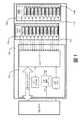
図1は、データストレージデバイス100を示すブロック図である。データストレージデバイス100は、コントローラボード102及び1つ以上のメモリボード104a及び104bを含むことができる。データストレージデバイス100は、インターフェイス108を介してホスト106と通信することができる。インターフェイス108は、ホスト106とコントローラボード102の間にあってもよい。コントローラボード102は、コントローラ110、DRAM 111、複数のチャネル112、電源モジュール114、及びメモリモジュール116を含むことができる。メモリボード104a及び104bは、各メモリボード上に複数のフラッシュメモリチップ118a及び118bを含むことができる。メモリボード104a及び104bはまた、メモリデバイス120a及び120bを含むことができる。 FIG. 1 is a block diagram showing a
一般に、データストレージデバイス100は、フラッシュメモリチップ118a及び118b上にデータを格納するように構成されてもよい。ホスト106は、フラッシュメモリチップ118a及び118bとの間でデータの書き込み及び読み取りを行うことができ、さらにフラッシュメモリチップ118a及び118bに関してその他の操作を実行させるようにすることができる。ホスト106とフラッシュメモリチップ118a及び118bとの間のデータの読み取り及び書き込み、並びにその他の操作は、コントローラボード102上のコントローラ110を通じて処理され、制御されてもよい。コントローラ110は、ホスト106からコマンドを受信して、メモリボード104a及び104b上のフラッシュメモリチップ118a及び118bを使用してそれらのコマンドを実行させてもよい。ホスト106とコントローラ110との間の通信は、インターフェイス108を通じて行われてもよい。コントローラ110は、チャネル112を使用して、フラッシュメモリチップ118a及び118bと通信することができる。 In general,
コントローラボード102は、DRAM 111を含むことができる。DRAM 111は、コントローラ110に機能的に結合されてもよく、情報を格納するために使用されてもよい。たとえば、DRAM 111は、論理アドレスから物理アドレスへのマップ及び不良ブロックの情報を格納するために使用されてもよい。DRAM 111はまた、ホスト106とフラッシュメモリチップ118a及び118bとの間のバッファとして機能するように構成されてもよい。 The
1つの例示的な実施態様において、コントローラボード102及び各々のメモリボード104a及び104bは、物理的に別個のプリント基板(PCB)である。メモリボード104aは、コントローラボード102のPCBに機能的に接続されている1つのPCB上にあってもよい。たとえば、メモリボード104aは、コントローラボード102に物理的及び/又は電気的に接続されてもよい。同様に、メモリボード104bは、メモリボード104aから分離されたPCBでもよく、コントローラボード102のPCBに機能的に接続されてもよい。たとえば、メモリボード104bは、コントローラボード102に物理的及び/又は電気的に接続されてもよい。 In one exemplary embodiment, the
メモリボード104a及び104bは各々、コントローラボード102から別個に切断されて取り外し可能であってもよい。たとえば、メモリボード104aは、コントローラボード102から切断されて、別のメモリボード(図示せず)に置き換えられてもよく、その別のメモリボードはコントローラボード102に機能的に接続される。この例において、メモリボード104a及び104bのいずれか又は両方は、他のメモリボードが同じコントローラボード102及びコントローラ110で動作できるように、他のメモリボードでスワップアウトされてもよい。 Each of the
1つの例示的な実施態様において、コントローラボード102及び各々のメモリボード104a及び104bは、ディスクドライブフォームファクタで物理的に接続されてもよい。ディスクドライブフォームファクタは、たとえば3.5”ディスクドライブフォームファクタ及び2.5”ディスクドライブフォームファクタのような、さまざまなサイズを含むことができる。 In one exemplary embodiment, the
1つの例示的な実施態様において、コントローラボード102及び各々のメモリボード104a及び104bは、高密度ボールグリッドアレイ(ball grid array)(BGA)コネクタを使用して電気的に接続されてもよい。たとえば、ファインボールグリッドアレイ(fine ball grid array)(FBGA)コネクタ、ウルトラファインボールグリッドアレイ(ultra fine ball grid array)(UBGA)コネクタ、及びマイクロボールグリッドアレイ(micro ball grid array)(MBGA) コネクタを含むその他のBGAコネクタの変種が使用されてもよい。その他のタイプの電気接続手段が使用されてもよい。 In one exemplary embodiment, the
インターフェイス108は、コントローラ110とホスト106との間の高速インターフェイスを含むことができる。高速インターフェイスは、ホスト106とフラッシュメモリチップ118a及び118bとの間のデータの高速転送を可能にすることができる。1つの例示的な実施態様において、高速インターフェイスは、Peripheral Component Interconnect Express(PCIe)インターフェイスを含むことができる。たとえば、PCIeインターフェイスは、PCIe x4インターフェイス又はPCIe x8インターフェイスであってもよい。PCIeインターフェイス108は、ホスト106へのPCIeコネクタケーブルアセンブリを含むことができる。この例において、110は、ホスト106とインターフェイス108との間のインターフェイスをとるように構成されたインターフェイスコントローラを含むことができる。インターフェイスコントローラは、PCIeエンドポイントコントローラを含むことができる。その他の高速インターフェイス、コネクタ及びコネクタアセンブリが使用されてもよい。 Interface 108 may include a high speed interface between controller 110 and host 106. The high speed interface may allow high speed transfer of data between the host 106 and the
1つの例示的な実施態様において、コントローラボード102とメモリボード104a及び104b上のフラッシュメモリチップ118a及び118bとの間の通信は、複数のチャネル112に配置されて構成されてもよい。各々のチャネル112は、1つ以上のフラッシュメモリチップ118a及び118bと通信することができる。コントローラ110は、ホスト106から受信されたコマンドが、各々のチャネル112を使用して、同時に、又は少なくとも実質的に同時にコントローラ110によって実行されうるように構成されてもよい。このように、複数のコマンドは、異なるチャネル112で同時に実行することができ、データストレージデバイス100のスループットを向上させることができる。 In one exemplary embodiment, communication between the
図1の例において、20個のチャネル112が示される。完全な実線は、コントローラ110とメモリボード104a上のフラッシュメモリチップ118aとの間の10個のチャネルを示す。実線及び破線の混合線は、コントローラ110とメモリボード104b上のフラッシュメモリチップ118bとの間の10個のチャネルを示す。図1に示すように、各々のチャネル112は、複数のフラッシュメモリチップをサポートすることができる。たとえば、各々のチャネル112は、最大32個のフラッシュメモリチップをサポートすることができる。1つの例示的な実施態様において、20個のチャネルは各々、6個のフラッシュメモリチップをサポートして通信するように構成されてもよい。この例において、各々のメモリボード104a及び104bは、それぞれ60個のフラッシュメモリチップを含むことができる。フラッシュメモリチップ118a及び118bのタイプ及び数に応じて、データストレージ100デバイスは、最大多数テラバイトのデータまで格納するように構成されてもよい。 In the example of FIG. 1, 20
コントローラ110は、マイクロコントローラ、FPGAコントローラ、その他のタイプのコントローラ、又はそれらのコントローラの組み合わせを含むことができる。1つの例示的な実施態様において、コントローラ110はマイクロコントローラである。マイクロコントローラは、ハードウェア、ソフトウェア、又はハードウェア及びソフトウェアの組み合わせで実施されてもよい。たとえば、マイクロコントローラは、実行されると、特定の方法でマイクロコントローラに実行させることができる命令を含むコンピュータプログラム製品がメモリ(たとえば、メモリモジュール116)からロードされてもよい。マイクロコントローラは、インターフェイス108を使用してホスト106からコマンドを受信し、コマンドを実行するように構成されてもよい。たとえば、コマンドは、フラッシュメモリチップ118a及び118bを使用してデータのブロックの読み取り、書き込み、コピー、及び削除を行うコマンド、並びにその他のコマンドを含むことができる。 The controller 110 can include a microcontroller, an FPGA controller, other types of controllers, or a combination of these controllers. In one exemplary embodiment, controller 110 is a microcontroller. The microcontroller may be implemented in hardware, software, or a combination of hardware and software. For example, when the microcontroller is executed, a computer program product may be loaded from memory (eg, memory module 116) that includes instructions that can cause the microcontroller to execute in a particular manner. The microcontroller may be configured to receive commands from the host 106 using the interface 108 and execute the commands. For example, the commands may include commands that use
もう1つの例示的な実施態様において、コントローラ110はFPGAコントローラである。FPGAコントローラは、ハードウェア、ソフトウェア、又はハードウェア及びソフトウェアの組み合わせで実施されてもよい。たとえば、FPGAコントローラは、実行されると、特定の方法でFPGAコントローラに実行させることができる命令を含むファームウェアがメモリ(たとえば、メモリモジュール116)からロードされてもよい。FPGAコントローラは、インターフェイス108を使用してホスト106からコマンドを受信し、コマンドを実行するように構成されてもよい。たとえば、コマンドは、フラッシュメモリチップ118a及び118bを使用してデータのブロックの読み取り、書き込み、コピー、及び削除を行うコマンド、並びにその他のコマンドを含むことができる。 In another exemplary embodiment, controller 110 is an FPGA controller. The FPGA controller may be implemented in hardware, software, or a combination of hardware and software. For example, when executed, the FPGA controller may be loaded from memory (eg, memory module 116) with instructions that can cause the FPGA controller to execute in a particular manner. The FPGA controller may be configured to receive commands from the host 106 using the interface 108 and execute the commands. For example, the commands may include commands that use
メモリモジュール116は、コントローラ110にロードされうるデータを格納するように構成されてもよい。たとえば、メモリモジュール116は、FPGAコントローラの1つ以上のイメージを格納するように構成されてもよく、イメージはFPGAコントローラによって使用されるファームウェアを含む。メモリモジュール116は、ホスト106と通信するために、ホスト106とのインターフェイスをとることができる。メモリモジュール116は、ホスト106と直接インターフェイスをとることができる、及び/又はコントローラ110を通じてホスト106と間接的にインターフェイスをとることができる。たとえば、ホスト106は、ファームウェアの1つ以上のイメージを、格納のためにメモリモジュール116に伝達することができる。1つの例示的な実施態様において、メモリモジュール116は、電気的消去可能プログラマブルROM(electrically erasable programmable read-only memory)(EEPROM)を含む。メモリモジュール116はまた、その他のタイプのメモリモジュールを含むことができる。 The
メモリボード104a及び104bは、さまざまなタイプのフラッシュメモリチップ118a及び118bで動作するように構成されてもよい。1つの例示的な実施態様において、フラッシュメモリチップ118a及びフラッシュメモリチップ118bは、電源モジュール114から同じ電圧を必要とすること、及び同じフラッシュメモリチップベンダーのものであることを含む同じタイプのフラッシュメモリチップであってもよい。ベンダー及び製造元という用語は、本文書全体を通じて同義的に使用される。
1つの例示的な実施態様において、メモリボード104a上のフラッシュメモリチップ118aは、メモリボード104b上のフラッシュメモリチップ118bとは異なるタイプであってもよい。たとえば、メモリボード104aはSLC NANDフラッシュメモリチップを含むことができ、メモリボード104bはMLC NANDフラッシュメモリチップを含むことができる。もう1つの例において、メモリボード104aはあるフラッシュメモリチップ製造元によるラッシュメモリチップを含むこともあり、メモリボード104bは別のフラッシュメモリチップ製造元によるフラッシュメモリチップを含むこともある。すべて同じタイプのフラッシュメモリチップを備えるか、又は異なるタイプのフラッシュメモリチップを備えるという柔軟性があるため、データストレージデバイス100は、ホスト106に使用されているさまざまなアプリケーションに合わせて調整することができる。 In one exemplary embodiment, the
もう1つの例示的な実施態様において、メモリボード104a及び104bは、同じメモリボード上に異なるタイプのフラッシュメモリチップを含むことができる。たとえば、メモリボード104aは、同じPCB上にSLC NANDチップとMLC NANDチップの両方を含むことができる。同様に、メモリボード104bは、SLC NANDチップとMLC NANDチップの両方を含むことができる。このように、データストレージデバイス100は、ホスト106の仕様に適合するように有利に調整されてもよい。 In another exemplary embodiment, the
もう1つの例示的な実施態様において、メモリボード104a及び104bは、フラッシュメモリ以外のチップを含む、その他のタイプのメモリデバイスを含むことができる。たとえば、メモリボード104a及び104bは、たとえばダイナミックRAM(DRAM)及びスタティックRAM(SRAM)のようなランダムアクセスメモリ(RAM)、並びにその他のタイプのRAM及びその他のタイプのメモリデバイスを含むこともできる。1つの例示的な実施態様において、メモリボード104a及び104はいずれも、RAMを含むことができる。もう1つの例示的な実施態様において、メモリボードの一方はRAMを含み、もう一方のメモリボードはフラッシュメモリチップを含むことができる。また、メモリボードの一方は、RAM及びフラッシュメモリチップの両方を含むことができる。 In another exemplary embodiment, the
メモリボード104a及び104b上のメモリモジュール120a及び120bは、それぞれフラッシュメモリチップ118a及び118bに関連する情報を格納するために使用されてもよい。1つの例示的な実施態様において、メモリモジュール120a及び120bは、フラッシュメモリチップのデバイス特性を格納することができる。デバイス特性は、チップがSLCチップ又はMLCのいずれであるか、チップがNAND又はNORチップのいずれであるか、チップセレクトの数、ブロックの数、ブロックあたりのページの数、ページあたりのバイトの数、及びチップの速度を含むことができる。
1つの例示的な実施態様において、メモリモジュール120a及び120bは、シリアルEEPROMを含むことができる。EEPROMは、デバイス特性を格納することができる。デバイス特性は、任意の所定のタイプのフラッシュメモリチップに対して1回コンパイルされてもよく、適切なEEPROMイメージがデバイス特性と共に生成されてもよい。メモリボード104a及び104bがコントローラボード102に機能的に接続される場合、デバイス特性は、コントローラ110が制御しているフラッシュメモリチップ118a及び118bのタイプをコントローラ110が自動的に認識できるように、EEPROMから読み取られてもよい。加えて、デバイス特性は、特定の1つ以上のタイプのフラッシュメモリチップ118a及び118bの適切なパラメータにコントローラ110を構成するために使用されてもよい。 In one exemplary implementation, the
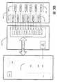
上記で説明されるように、コントローラ110は、FPGAコントローラを含むことができる。図2を参照すると、FPGAコントローラ210を示す例示的なブロック図が示される。FPGAコントローラは、図1のコントローラ110に関して上記で説明されたように動作するよう構成されてもよい。FPGAコントローラ210は、複数のチャネル112をフラッシュメモリチップ218に接続するために複数のチャネルコントローラ250を含むことができる。フラッシュメモリチップ218は、各々のチャネルコントローラ250に接続する複数のフラッシュメモリチップとして示される。フラッシュメモリチップ218は、図1の別個のメモリボード104a及び104b上にある、図1のフラッシュメモリチップ118a及び118bの代表である。別個のメモリボードは、図2の例には示されていない。FPGAコントローラ210は、PCIeインターフェイスモジュール208、双方向ダイレクトメモリアクセス(DMA)コントローラ252、ダイナミックランダムアクセスメモリ(DRAM)コントローラ254、コマンドプロセッサ/キュー256、及び情報及び構成インターフェイスモジュール258を含むことができる。 As described above, the controller 110 can include an FPGA controller. Referring to FIG. 2, an exemplary block diagram illustrating the
情報は、インターフェイスを使用してホスト(たとえば、図1のホスト106)との間で伝達されてもよい。図2のこの例において、FPGAコントローラ210は、ホスト及びPCIeインターフェイスモジュール208と通信するためにPCIeインターフェイスを含む。PCIeインターフェイスモジュール208は、ホストからコマンドを受信して、ホストにコマンドを送信するように、配置され構成されてもよい。PCIeインターフェイスモジュール208は、ホストとデータストレージデバイスとの間のデータフロー制御をもたらすことができる。PCIeインターフェイスモジュール208は、ホストとコントローラ210、及び最終的にはフラッシュメモリチップ218との間のデータの高速転送を可能にすることができる。1つの例示的な実施態様において、PCIeインターフェイス及びPCIeインターフェイスモジュール208は、64ビットバスを含むことができる。双方向ダイレクトメモリアクセスDMAコントローラ252は、PCIeインターフェイスモジュール208とコマンドプロセッサ/キュー256間のバスの動作を制御するように配置され構成されてもよい。 Information may be communicated to a host (eg, host 106 of FIG. 1) using an interface. In this example of FIG. 2, the
双方向DMAコントローラ252は、PCIeインターフェイス208、及び各々のチャネルコントローラ250とのインターフェイスをとるように構成されてもよい。双方向DMAコントローラ252は、ホスト106とフラッシュメモリチップ218との間の双方向ダイレクトメモリアクセスを可能にする。
DRAMコントローラ254は、論理アドレスから物理アドレスへの変換を制御するように配置され構成されてもよい。たとえば、ホストが論理アドレスを使用してメモリスペースをアドレス指定する実施態様において、DRAMコントローラ254は、コマンドプロセッサ/キュー256が、ホストに使用されている論理アドレスを、フラッシュメモリチップ218との間で書き込み中又は読み取り中のデータに関連するフラッシュメモリチップ218内の実際の物理アドレスに変換する操作を補助することができる。ホストから受信された論理アドレスは、フラッシュメモリチップ218の1つの位置の物理アドレスに変換されてもよい。同様に、フラッシュメモリチップ218の1つの位置の物理アドレスは、論理アドレスに変換されて、ホストに伝達されてもよい。 The
コマンドプロセッサ/キュー256は、PCIeインターフェイスモジュール208を通じてホストからコマンドを受信し、チャネルコントローラ250を通じてコマンドの実行を制御するように、配置され構成されてもよい。コマンドプロセッサ/キュー256は、実行されるべき複数のコマンドのキューを保持し、最も古いコマンドが確実に最初に処理されるように番号付きリストを使用してコマンドを順序付けることができる。コマンドプロセッサ100は、同じフラッシュメモリチップに指定されているコマンドの順序を保持することができ、異なるフラッシュメモリチップに指定されているコマンドを再配列することができる。このように、複数のコマンドは同時に実行されてもよく、各々のチャネル112は、同時に、又は少なくとも実質的に同時に使用されてもよい。 The command processor / queue 256 may be arranged and configured to receive commands from the host through the PCIe interface module 208 and control the execution of commands through the
コマンドプロセッサ/キュー256は、異なるチャネル112のコマンドを順不同に処理して、チャネルごとのコマンド順序付けを保持するように構成されてもよい。たとえば、ホストから受信されて、異なるチャネルに指定されているコマンドは、コマンドプロセッサ/キュー256によって順不同に処理されてもよい。このように、チャネルはビジー状態の場合もある。同じチャネルで処理されるようにホストから受信されるコマンドは、コマンドがホストからコマンドプロセッサ/キュー256によって受信された順序で処理されてもよい。1つの例示的な実施態様において、コマンドプロセッサ/キュー256は、コマンドが確実に適時に実行されるようにするため、古いもの順でホストから受信されたコマンドのリストを保持するように構成されてもよい。 Command processor / queue 256 may be configured to process commands for
チャネルコントローラ250は、コマンドプロセッサ/キュー256からのコマンドを処理するように配置されて構成されてもよい。各々のチャネルコントローラ250は、複数のフラッシュメモリチップ218のコマンドを処理するように構成されてもよい。1つの例示的な実施態様において、各々のチャネルコントローラ250は、最大32個のフラッシュメモリチップ218のコマンドを処理するように構成されてもよい。
チャネルコントローラ250は、コマンドプロセッサ/キュー256によって指定された順序で、コマンドプロセッサ/キュー256からのコマンドを処理するように構成されてもよい。処理されうるコマンドの例は、フラッシュページの読み取り、フラッシュページのプログラミング、フラッシュページのコピー、フラッシュブロックの消去、フラッシュブロックのメタデータの読み取り、フラッシュメモリチップの不良ブロックのマッピング、及びフラッシュメモリチップのリセットを含むが、これらに限定されることはない。
情報及び構成インターフェイスモジュール258は、FPGAコントローラ210の構成情報を受信するために、メモリモジュール(たとえば、図1のメモリモジュール116)とのインターフェイスをとるように配置され構成されてもよい。たとえば、情報及び構成インターフェイスモジュール258は、ファームウェアをFPGAコントローラ210に提供するために、メモリモジュールから1つ以上のイメージを受信することができる。イメージ及びファームウェアへの変更は、ホストにより情報及び構成インターフェイスモジュール258を通じてコントローラ210に提供されてもよい。情報及び構成インターフェイスモジュール258を通じて受信された変更は、たとえば、PCIeインターフェイスモジュール208、双方向ダイレクトメモリアクセス(DMA)コントローラ252、DRAMコントローラ254、コマンドプロセッサ/キュー256、チャネルコントローラ250を含むコントローラ210のコンポーネントのいずれかに適用されてもよい。情報及び構成インターフェイスモジュール258は、1つ以上のレジスタを含むことができ、レジスタはホストからの命令により必要に応じて変更されてもよい。 Information and configuration interface module 258 may be arranged and configured to interface with a memory module (eg,
FPGAコントローラ210は、ホストと共に協働してコマンドを処理するように配置されて構成されてもよい。FPGAコントローラ210は、エラー訂正、不良ブロック管理、論理から物理へのマッピング、ガーベッジコレクション、消耗平準化、パーティショニング、及びフラッシュメモリチップ218に関連する低レベルフォーマッティングを実行することができるか、又は少なくともその操作を補助することができる。 The
図3Aは、第1のパーティション321及び第2のパーティション322に編成される複数のフラッシュメモリチップ318a、318b、318c、318d、318e、318f、318g、318h、318i、318j、318k、318lを有するデータストレージデバイス302を含む装置300を示す概略ブロック図である。第1及び第2のパーティション321及び322は、異なるカテゴリのディレクトリ及びファイルが異なるパーティションに格納されうるように、又は1つのパーティションが他のパーティションとは異なる目的で使用されうるように、データストレージデバイス302内のストレージスペースの異なる物理領域を定義する。第1のパーティションは、フラッシュメモリチップ318a〜fの第1のサブセットを含むことができ、第2のパーティションは、フラッシュメモリチップ318g〜lの第2のサブセットを含むことができるが、ここで両方のパーティションに属するフラッシュメモリチップはない。すなわち、パーティション321と322の境界は、個々のフラッシュメモリチップが2つ以上のパーティションに属することがないように、個々のフラッシュメモリチップの間に引かれる。 FIG. 3A shows data having a plurality of
データストレージデバイスを2つ以上のパーティションに編成することで、いくつかの目的にかなうことができる。たとえば、1つのパーティションに格納されたオペレーティングシステムファイルは、もう1つのパーティションに格納されたユーザファイルとは別個に保持することができる。動的かつ急速にサイズが変化することもあり、ファイルシステムを満杯にしてしまう可能性のあるキャッシュ及びログファイルは、1つのパーティションに格納して、異なるパーティションに格納されたその他のファイルとは別個に保持することもできる。パーティションは、マルチブートセットアップに使用されてもよく、それによりユーザは単一のコンピュータに複数のオペレーティングシステムを有することができる。たとえば、ユーザはLinux、Mac OS X、及びMicrosoft Windows、又はオペレーティングシステムを、同じデータストレージデバイスの異なるパーティションにインストールして、電源投入時に(ハードウェアによってサポートされる)任意のオペレーティングシステムへのブートを選択することができる。パーティションは、ファイルを保護又は隔離して、破損したファイルシステム又はオペレーティングシステムのインストールをより回復しやすくするために使用されてもよい。たとえば、1つのパーティションが破損しても、その他のファイルシステムは全く影響を受けていない場合、ストレージデバイス上のデータは引き続き救出可能である。読み取り専用データに別個のパーティションを使用することもまた、そのパーティション上のファイルシステムが破損してしまう可能性を低減する。パーティションはまた、より小さいファイルシステムがより効率的であるようなシステムにおいて全体的なコンピュータパフォーマンスを高めることができる。たとえば、1つのNTFSファイルシステムしか備えていない大規模なハードドライブは通常、非常に大型の順次アクセスのマスターファイルテーブル(MFT)を有し、このMFTを読み取るために要する時間は、より小さいパーティションの小さいMFTの場合よりも概して長くなる。 Organizing a data storage device into two or more partitions can serve several purposes. For example, operating system files stored in one partition can be kept separate from user files stored in another partition. Cache and log files, which can change size dynamically and rapidly, can fill up the file system, are stored in one partition and separate from other files stored in different partitions Can also be held. Partitions may be used for multi-boot setups so that a user can have multiple operating systems on a single computer. For example, a user can install Linux, Mac OS X, and Microsoft Windows, or an operating system on different partitions of the same data storage device, and boot to any operating system (supported by the hardware) at power up. You can choose. Partitions may be used to protect or isolate files and make it easier to recover a corrupted file system or operating system installation. For example, if one partition is corrupted and no other file system is affected, the data on the storage device can still be rescued. Using a separate partition for read-only data also reduces the possibility of file system corruption on that partition. Partitions can also increase overall computer performance in systems where smaller file systems are more efficient. For example, a large hard drive with only one NTFS file system typically has a very large sequential access master file table (MFT), and the time it takes to read this MFT is less than that of a smaller partition. Generally longer than with a small MFT.
もう1つの例示的な実施態様において、データストレージデバイス302は、データストレージデバイスから迅速に読み取られて、ホストに供給される必要のある膨大量のデータ(たとえば、多数ギガバイト又はテラバイトのデータ)を格納するために使用されてもよい。たとえば、データストレージデバイスは、クエリに応答してホストが取り出すことのできる大量の公的にアクセス可能な情報(たとえば、ワールドワイドウェブからの大量のウェブページのコーパス、電子版書籍の大規模なライブラリ、又は大量の通信を表すデジタル情報など)をキャッシュに入れるために使用されてもよい。つまり、関連データは、ホストによって発行される読み取りコマンドに応答して極めて迅速にアクセスされ、返されることが重要となりうる。しかし、データストレージデバイスに格納されている情報はまた、関連情報の変化に応じて情報を最新の状態に維持するために、常時更新される必要もある。たとえば、ストレージデバイス上の情報がウェブページのコーパスに関連する場合、ストレージデバイス上に格納されている情報は、ウェブページが変更されるごと、及び新しいウェブページが作成されるごとに更新される必要もある。 In another exemplary embodiment, the
そのようなシステムにおいて、パーティション化されたフラッシュメモリデータストレージデバイス302は、並外れたパフォーマンスを提供することができる。フラッシュメモリストレージデバイスにおいて、フラッシュメモリチップへの書き込み操作は、フラッシュメモリチップからの読み取り操作よりも、はるかに長い時間を要する(たとえば、10倍〜100倍長い)。したがって、データストレージデバイスのチップ318a〜lを2つ以上のパーティションに編成し、パーティションは異なるチップ間の境界で定義されるようにすることで、迅速な読み取り操作を確保し、しかもデータストレージデバイスに格納されている情報はリアルタイムで更新される方法をもたらす。たとえば、両パーティション321及び322は、クエリに応答して供給されるべきデータのコーパス(たとえば、ウェブページのコーパス)を格納するために使用されてもよく、個々のパーティションは、要求への対応と新しい情報による更新とを繰り返すことができる。たとえば、第1の時限において、第1のパーティション321は、ホストに情報(たとえば、ユーザクエリに応答して要求されうる情報)を提供するために使用されてもよく、その間、第2のパーティション322上のデータは(たとえば、ウェブページのコーパスへの変更又は追加に応答して)更新される。次いで、第2の時限において、最近更新された第2のパーティション322は、ホストに情報を提供するために使用されてもよく、その間、第1のパーティション321上のデータは更新される。データを常に読み取り専用デバイスとして機能するパーティションから供給することができるように、このプロセスを繰り返すことができる。したがって書き込みコマンドによって速度が低下することなくホストからの読み取りコマンドに極めて迅速に応答することができ、しかもその間に他のパーティションは新しい情報で更新される。個々のフラッシュメモリチップが1つのパーティションのみに含まれるようにパーティションを定義することで、データの書き込みと読み取りが実質的に同時に行われるフラッシュチップ(ホスト350からの読み取り要求への応答に遅延を生じる原因となる)がないようにする。 In such a system, the partitioned flash memory
上記で説明されるように、メモリチップ318a〜lは、FPGAコントローラ310を含むことができるコントローラに接続されてもよい。FPGAコントローラは、図1のコントローラ110、又は図2のFPGA 210に関して上記で説明されているように動作するよう構成されてもよい。FPGAコントローラ310は、複数のチャネル112をフラッシュメモリチップ318a〜lに接続するために複数のチャネルコントローラ312a、312b、312c、312d、312e、312fを含むことができる。言うまでもなく、上記で説明されているように、ストレージデバイスは、12個よりも多いフラッシュメモリチップ、6個よりも多いチャネルコントローラを含むことができ、2個よりもはるかに多くのフラッシュメモリチップは、物理チャネルにわたりチャネルコントローラに機能的に接続されてもよい。したがって、図3A及び図3Bに示される実施態様は、説明を明確にするため単に概略を示したものにすぎない。 As described above, the
1つの実施態様において、チャネルコントローラ312a、312b、312c、312d、312e、312fは、各パーティション321及び322の一部であるフラッシュメモリチップに機能的に接続されるチャネルを制御することができる。たとえば、チャネルコントローラ312aは、第1のパーティション321の一部であるメモリチップ318a、及びまた第2のパーティション322の一部であるメモリチップ318gに、機能的に接続されてもよい。そのような構成において、第1のパーティション321の少なくとも1つのメモリチップは、データストレージデバイス302とホストとの間の各通信チャネルに接続され、第2のパーティション322の少なくとも1つのメモリチップは、データストレージデバイス302とホスト350との間の各通信チャネルに接続される。そのような構成は、パーティション321又は322とホストとの間の通信の最大並列処理につながり、その結果データストレージデバイス302との間の高速読み取りアクセス及び高速書き込み時間をもたらすことができる。 In one embodiment,
もう1つの実施態様において、ほぼ半数のチャネルコントローラが第1のパーティションのフラッシュメモリチップに機能的に接続されてもよく、ほぼ半数のチャネルコントローラが第2のパーティションのフラッシュメモリチップに機能的に接続されてもよい。 In another embodiment, approximately half of the channel controllers may be functionally connected to the flash memory chip in the first partition, and approximately half of the channel controllers are functionally connected to the flash memory chip in the second partition. May be.
図3Bに示されるもう1つの実施態様において、フラッシュメモリチップ318a、318b、318c、318d、318e、318f、318g、318h、318i、318j、318k、318lは、第1のパーティション331、第2のパーティション322、第3のパーティション333、第4のパーティション334に編成されてもよく、ここで異なるカテゴリのディレクトリ及びファイルが異なるパーティションに格納されうるように、又は1つのパーティションが他のパーティションとは異なる目的で使用されうるように、異なるパーティションはデータストレージデバイス302内のストレージスペースの異なる物理領域を定義する。第1のパーティション331は、フラッシュメモリチップ318a〜cの第1のサブセットを含むことができる。第2のパーティション332は、フラッシュメモリチップ318d〜fの第2のサブセットを含むことができる。第3のパーティション333は、フラッシュメモリチップ318g〜iの第3のサブセットを含むことができる。第4のパーティション334は、フラッシュメモリチップ318j〜lの第4のサブセットを含むことができる。さまざまなパーティション331、332、333、及び334の中で、物理メモリアドレススペースが2つ以上のパーティションの一部である個々のフラッシュメモリチップはない。すなわち、パーティション331、332、333、及び334の間の境界は、個々のフラッシュメモリチップが2つ以上のパーティションに属することがないように、個々のフラッシュメモリチップの間に引かれる。 In another embodiment shown in FIG. 3B, the
図3Bのシステムにおいて、パーティション化されたフラッシュメモリデータストレージデバイス302は、たとえば、クエリに応答して供給されるべきデータのコーパス(たとえば、ウェブページのコーパス)を格納するために使用される場合、及び個々のパーティションが要求への対応と新しい情報による更新とを繰り返すことができる場合に、並外れたパフォーマンスを提供することができる。たとえば、第1の時限において、第1、第2、及び第3のパーティション331、332、及び333は、ホストに情報(たとえば、ユーザクエリに応答して要求されうる情報)を提供するために使用されてもよく、その間、第4のパーティション334上のデータは(たとえば、ウェブページのコーパスへの変更又は追加に応答して)更新される。次いで、第2の時限において、最近更新された第4のパーティション334は、第2及び第3のパーティション332及び332と共にホストに情報を提供するために使用されてもよく、その間、第1のパーティション331上のデータは更新される。したがって、各パーティション上のデータは、ラウンドロビンの方式で更新されてもよく、その間、クエリ要求は他のパーティションによって対応される。このプロセスは、データが常に、読み取り専用デバイスとして機能するパーティションから供給されるように繰り返されてもよく、したがって書き込みコマンドによって速度が低下することなくホストからの読み取りコマンドに極めて迅速に応答することができ、しかもその間他のパーティションは新しい情報で更新される。4つのパーティションを定義することで、1つのパーティションがもはや使用可能ではなくなるような、パーティション、チャネル、又は個々のメモリチップの障害が生じる場合、残りの3つのパーティションが引き続き使用されて、各々の残りのパーティションが交代で更新され、その間他の残りのパーティションがデータ要求に対応するデータストレージデバイスを提供することができるように、データストレージデバイス上に格納されている情報の冗長性がもたらされる。 In the system of FIG. 3B, a partitioned flash memory
上記で説明されるように、データストレージデバイス302は、たとえばPCIeインターフェイスのような高速インターフェイスであってもよい、インターフェイス308を通じてホスト350に接続されてもよい。ホストは、たとえば、プロセッサ352、第1のメモリ354、第2のメモリ356、及びパーティションエンジン360を含むことができる。第1のメモリ354は、たとえば、プロセッサ352によって実行されうる機械可読の実行可能コード命令を格納するように適合される不揮発性メモリデバイス(たとえば、ハードディスク)を含むことができる。第1のメモリ354に格納されるコード命令は、第2のメモリ(たとえば、ランダムアクセスメモリのような揮発性メモリ)356にロードすることができ、ここでコード命令はプロセッサ352によって実行されて、メモリデバイス検出エンジン358及びパーティションエンジン360を作成することができる。第2のメモリは、ユーザモードアプリケーションに専用の「ユーザスペース」の論理ブロック、及びユーザレベルアプリケーションがそれらの機能を実行するために制御する必要のある低レベルリソースの実行に専用の「カーネルスペース」364の論理ブロックを含むことができる。メモリデバイス検出エンジン358及びパーティションエンジン360は、第2のメモリ356のカーネルスペース364に常駐することができる。 As described above, the
構成検出エンジン358は、データストレージデバイス302上のフラッシュメモリチップ318の数を検出するように構成されてもよく、パーティションエンジン360は、データストレージデバイスの第1のパーティション321及び第2のパーティション322を定義するように構成されてもよい。したがって、ホスト350で稼働する構成検出エンジン358及びパーティションエンジン360は、ホストが、データストレージデバイス302のハードウェアデバイスプロパティを発見し、次いでパーティション321及び322をホストを介して定義するために使用することができる。1つの実施態様において、構成検出エンジン358は、データストレージデバイスにクエリコマンドを発行することができ、データストレージデバイスは、クエリコマンドに応答して、たとえばフラッシュメモリチップ318の数、各チップの(たとえば、バイトで測定された)サイズ、データストレージデバイスのチャネルの数、各チャネルコントローラ312a〜eが機能的に接続されているフラッシュメモリチップに関する情報をホストに返すことができる。そのような情報は、FPGA 310上のEEPROM 116及び/又はデータストレージデバイス302のフラッシュボードのEEPROM 120aに格納されてもよい。構成検出エンジンは、EEPROM 116又はEEPROM 120aをポーリングして(たとえば、ホスト350のブートアップ作業の間)、データストレージデバイスにそのような情報をホスト350に返させるようにすることができる。もう1つの実施態様において、ホストは、フラッシュメモリチップ318をポーリングして、たとえばフラッシュメモリチップ318の数、各チップの(たとえば、バイトで測定された)サイズ、データストレージデバイスのチャネルの数、各チャネルコントローラ312a〜eが機能的に接続されているフラッシュメモリチップに関する情報を提供することができる。 The
パーティションエンジン360は、フラッシュメモリチップ318の数、各フラッシュチップのサイズ、チャネルの数、及び各チャネルが機能的に接続されているメモリチップに関する情報を、メモリデバイス検出エンジン358から受信することができ、この情報に基づいて、パーティションエンジンは、データストレージデバイス302の第1のパーティション321及び第2のパーティション322を定義することができる。ホスト350で稼働しているパーティションエンジンは、メモリチップ318の第1のサブセットから取り出されたメモリブロックを含むように第1のパーティションを定義し、メモリチップ318の第2のサブセットから取り出されたメモリブロックを含むように第2のパーティションを定義することができ、第1のサブセットは第2のサブセットの個々のフラッシュチップを含むことはなく、第2のサブセットは第1のサブセットの個々のフラッシュチップを含むことはない。次いで、パーティションエンジン360は、物理メモリブロックアドレス(たとえば、一意のチャネル番号、一意のフラッシュメモリチップ番号、及びフラッシュメモリチップ内のブロックアドレスを含むこともある)を、ホスト350で稼働しているユーザスペースアプリケーションが、論理スペースアドレスを参照して、データストレージデバイス302からデータを読み取り、データストレージデバイス302にデータを書き込むことができるように、ユーザスペースで稼働しているアプリケーションプログラムによって使用されうる論理アドレスにマップすることができる。 The
複数のパーティションのパーティション方式が定義されて、データがデータストレージデバイス100のフラッシュメモリチップに格納された後、デバイスは、デバイスが後にブートされるときに、ホストが使用するようパーティション方式をホスト106に伝達することができるように、たとえばメモリ116に、パーティション方式に関する情報を格納することができる。たとえば、デバイスは、デバイスのフラッシュメモリチップの数を含むデータストレージデバイスの物理構成に関する情報、及びどのフラッシュメモリチップ及びチャネルがメモリ116のどのパーティションに関連付けられているかを含むパーティション方式に関する情報を保持することができる。次いで、ホスト106及びデータストレージデバイス100を含むシステムがブートされるとき、ストレージデバイス100は、たとえばホスト106の構成検出エンジン358によって実行された読み取り操作に応答して、この情報をホスト106に伝達することができる。次いで、ホスト106のパーティションエンジン360は、ホストで稼働しているオペレーティングシステム及びアプリケーションのパーティションを定義することができる。たとえば、パーティションエンジン360は、ストレージデバイス100から読み取られた情報に基づいて第1及び第2のパーティションを定義することができ、ここで第1及び第2のパーティションは同じメモリチップを含むことはない。パーティションエンジン360はまた、ユーザレベルアプリケーションプログラムが次いでストレージデバイス100のフラッシュメモリチップの物理メモリアドレスにマップされる論理アドレスを使用することができるように、第1及び第2のパーティションの論理メモリから物理メモリへのマップを割り振ることもできる。 After the partition scheme for multiple partitions is defined and the data is stored in the flash memory chip of the
パーティションエンジン360はまた、複数のフラッシュメモリチップの第3のサブセットを含むようにデータストレージデバイスの第1のパーティションを再定義するために使用されてもよく、第3のサブセットは第1のサブセットとは異なり、第3のサブセットは第2のサブセットのフラッシュメモリチップを含むことはなく、第2のサブセットは第3のサブセットのフラッシュメモリチップを含むことはない。たとえば、図3A及び図3Bを参照すると、ユーザは、図3Aに示される元のパーティション方式が自身の必要性を満たしてはいないと判断することができ、したがって、パーティション321及び322を再定義するため(たとえば、特定のパーティションにより多く又は少ないフラッシュメモリチップを含むように)、又は追加のパーティションを方式に追加するためにホストを使用することができる。1つの実施態様において、第1のパーティション321は、パーティション331及び333として再定義されてもよい。コントローラ310によって事前定義されるか、又はプリロード済みのパーティション方式をユーザに強制的に受け入れさせるのではなく、ユーザがホストを通じてパーティションを定義できるようにすることで、ユーザには所望のとおりパーティションを定義して、必要なときにパーティション方式を変更する柔軟性がもたらされる。もう1つの実施態様において、フラッシュメモリチップの1つ、たとえば318aの差し迫った障害が、ホストによって検出されることもあり、この情報に応答して、パーティションエンジンは、パーティションからフラッシュメモリチップ318aを除外するように、すなわちメモリチップ318aを除く当初定義された第1のパーティションのように、第1のパーティション321を再定義することができる。したがって、任意のパーティションの数が(ストレージデバイス100のフラッシュメモリチップ118a及び118bの数まで)定義されてもよく、パーティション方式内の異なるパーティションは、異なる数のフラッシュメモリチップを含むことができ、異なる量のメモリスペースを含むことができる。
ホストはまた、カーネル364に存在し、データストレージデバイス302に書き込まれるべきデータに物理メモリアドレスを割り当てることができるアドレス割り当てエンジン366を含むこともできる。たとえば、ユーザスペース363で稼働しているアプリケーションは、データがホスト350からデータストレージデバイス302に書き込まれるよう要求することができ、ユーザスペースアプリケーションは、データが特定の論理メモリアドレスに書き込まれるよう指定することができる。アドレス割り当てエンジン366は、論理アドレスを、たとえばデータが書き込まれるべき特定のチャネル、データが書き込まれるべき指定されたチャネルに機能的に接続された特定のフラッシュメモリチップ、及びデータが書き込まれるべき指定されたメモリチップの特定の物理ブロックアドレスを含むことができる物理アドレスに変換することができる。そのような実施態様において、論理アドレスの物理メモリスペースアドレスへの変換は、FPGA 210のDRAMコントローラ254の役割が軽減されるか又は重要ではないように、アドレス割り当てエンジン366によって実行されてもよい。 The host may also include an
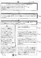
図4は、図1のデータストレージデバイスのパーティション化の例示のプロセス400を示す例示的な流れ図であり、ここでデバイスは複数のフラッシュメモリチップを含む。プロセス400は、データストレージデバイス内のフラッシュメモリチップの数を決定することを含むことができる(402)。たとえば、構成検出エンジンは、データストレージデバイス内のフラッシュメモリチップの数に関する情報を収集するために、データストレージデバイスにクエリを行うことができる。データストレージデバイスの第1のパーティションは、データストレージデバイスに結合されたホストを介して、定義されてもよく、第1のパーティションは複数のフラッシュメモリチップの第1のサブセットを含む(404)。データストレージデバイスの第2のパーティションは、ホストを介して定義されてもよく、第2のパーティションは複数のフラッシュメモリチップの第2のサブセットを含む(406)。このプロセスの結果として、第1のサブセットが第2のサブセットのフラッシュメモリチップを含むことはなく、第2のサブセットが第1のサブセットのフラッシュメモリチップを含まないことが保証される。 FIG. 4 is an exemplary flow diagram illustrating an
オプションで、プロセス400は、第2のパーティションからのデータの読み取り中に、データを第1のパーティションに書き込むこと(408)を含むことができる。データストレージデバイス内のフラッシュメモリチップの数を決定することは、データストレージデバイス内のフラッシュメモリチップの数を指示する情報をデータストレージデバイスからホストに送信すること(410)を含むことができる。ホストからデータを書き込むデータストレージデバイス内のアドレス位置は、ホストにおいて定義されてもよく、アドレス位置は、データが複数のメモリチップのうちの特定の1つに書き込まれることを指定する(412)。 Optionally, the
データストレージデバイスが、ホストと複数のフラッシュメモリチップ間のデータの通信のための複数の物理チャネルを含み、各チャネルは異なる複数のメモリチップに機能的に接続される場合、プロセス400はさらに、物理チャネルの数を決定すること(414)と、チャネルの第1のサブセットを決定することであって、チャネルの第1のサブセットのチャネルは、メモリチップの第1のサブセットのメモリチップにのみ機能的に接続されること(416)と、チャネルの第2のサブセットを決定することであって、チャネルの第2のサブセットのチャネルは、メモリチップの第2のサブセットのメモリチップにのみ機能的に接続されること(418)と、ホストにおいて、ホストからデータを書き込むデータストレージデバイス内のアドレス位置を定義することであって、アドレス位置は、特定のチャネルを通じてデータが複数のメモリチップのうちの特定の1つに書き込まれることを指定すること(420)とを含むことができる。加えて、プロセス400は、データストレージデバイスに結合されたホストを介して、データストレージデバイスの第1のパーティションが複数のフラッシュメモリチップの第3のサブセットを含むように再定義すること(422)を含むことができる。 If the data storage device includes multiple physical channels for communication of data between the host and multiple flash memory chips, each channel being functionally connected to a different multiple memory chip, the
図5は、複数のフラッシュメモリチップを含むデータストレージデバイスをパーティション化する例示的なプロセス500を示すもう1つの例示的な流れ図である。プロセス500は、データストレージデバイス内のフラッシュメモリチップの数を含む、データストレージデバイスの物理構成を読み取ること(502)を含むことができる。プロセスはまた、データストレージデバイスのパーティション化方式を読み取ること(504)を含むことができる。たとえば、構成検出エンジンは、データストレージデバイスのメモリ116から物理構成及びパーティション化方式を読み取ることができる。データストレージデバイスに結合されたホストは、データストレージデバイスの第1のパーティションを定義することができ、第1のパーティションは複数のフラッシュメモリチップの第1のサブセットを含み(506)、第1のパーティションの論理メモリから物理メモリへのマップが割り振られてもよい(508)。ホストは、データストレージデバイスの第2のパーティションを定義することができ、第2のパーティションは複数のフラッシュメモリチップの第2のサブセットを含み(510)、第1のサブセットは第2のサブセットのフラッシュメモリを含むことはなく、第2のサブセットは第1のサブセットのフラッシュメモリチップを含むことはなく、第2のパーティションの論理メモリから物理メモリへのマップが割り振られてもよい(512)。 FIG. 5 is another example flow diagram illustrating an
本明細書において説明されるさまざまな技法の実施態様は、デジタル電子回路において、又はコンピュータハードウェア、ファームウェア、ソフトウェア、若しくはその組み合わせで実施されてもよい。実施態様は、コンピュータプログラム製品として、すなわち、たとえばプログラム可能プロセッサ、コンピュータ、又は複数のコンピュータなどのデータ処理装置により実行するため、若しくはその動作を制御するための、たとえば機械可読ストレージデバイスなどの情報担体において実体的に具現されるコンピュータプログラムとして、実施されてもよい。上記で説明される(1つ以上の)コンピュータプログラムのような、コンピュータプログラムは、コンパイル済み又は解釈済みの言語を含む任意の形態のプログラミング言語で記述されてもよく、スタンドアロンのプログラムとして、又はモジュール、コンポーネント、サブルーチン、若しくはコンピューティング環境において使用に適した他のユニットとしてなど、任意の形態で配置されてもよい。コンピュータプログラムは、1つのサイトにおける1つのコンピュータ上、又は複数サイトに分散されて通信ネットワークにより相互接続された複数コンピュータ上で実行されるように配置されてもよい。 Implementations of the various techniques described herein may be implemented in digital electronic circuitry or in computer hardware, firmware, software, or combinations thereof. An embodiment is an information carrier, such as a machine readable storage device, for example as a computer program product, i.e. for execution by a data processor such as a programmable processor, a computer or a plurality of computers or for controlling its operation. The present invention may be implemented as a computer program tangibly embodied in A computer program, such as the computer program (s) described above, may be written in any form of programming language, including compiled or interpreted languages, as a stand-alone program or as a module , Components, subroutines, or any other unit suitable for use in a computing environment. The computer program may be arranged to be executed on one computer at one site or on a plurality of computers distributed over a plurality of sites and interconnected by a communication network.
方法ステップは、入力データを操作して出力を生成することにより機能を実行するようにコンピュータプログラムを実行している1つ以上のプログラム可能プロセッサによって実行されてもよい。たとえばFPGA又はASIC(特殊用途向け集積回路)などの特殊用途論理回路によって、方法ステップはまた実行されてもよく、装置は特殊用途論理回路として実施されてもよい。 Method steps may be performed by one or more programmable processors executing a computer program to perform functions by manipulating input data to produce output. The method steps may also be performed by a special purpose logic circuit such as an FPGA or ASIC (special purpose integrated circuit), and the apparatus may be implemented as a special purpose logic circuit.
コンピュータプログラムの実行に適したプロセッサは、一例として、汎用及び特殊用途マイクロプロセッサ、及び任意の種類のデジタルコンピュータの1つ以上のプロセッサを含む。一般に、プロセッサは、読み取り専用メモリ又はランダムアクセスメモリ、若しくはその両方から命令及びデータを受信する。コンピュータの要素は、命令を実行するための少なくとも1つのプロセッサと、命令及びデータを格納するための1つ以上のメモリデバイスを含むことができる。一般に、コンピュータはまた、たとえば磁気、光磁気ディスク、又は光ディスクなど、データを格納するための1つ以上の大容量ストレージデバイスを含むことができるか、又は大容量ストレージデバイスとの間でデータを受信又は転送若しくはその両方を行うように機能的に結合されてもよい。コンピュータプログラム命令及びデータを具現するために適した情報担体は、一例として、たとえばEPROM、EEPROM、及びフラッシュメモリデバイスのような半導体メモリデバイス;たとえば内蔵ハードディスク又はリムーバブルディスクのような磁気ディスク;光磁気ディスク;並びにCD-ROM及びDVD-ROMディスクを含む、あらゆる形態の不揮発性メモリを含む。プロセッサ及びメモリは、特殊用途論理回路によって補完されてもよいか、又は特殊用途論理回路に組み込まれてもよい。 Processors suitable for executing computer programs include, by way of example, general and special purpose microprocessors and one or more processors of any type of digital computer. Generally, a processor will receive instructions and data from a read-only memory or a random access memory or both. The computer elements can include at least one processor for executing instructions and one or more memory devices for storing instructions and data. In general, a computer may also include one or more mass storage devices for storing data, such as a magnetic, magneto-optical disk, or optical disk, or receive data from or to a mass storage device Or may be functionally coupled to perform forwarding or both. Information carriers suitable for embodying computer program instructions and data include, by way of example, semiconductor memory devices such as EPROM, EEPROM, and flash memory devices; magnetic disks such as internal hard disks or removable disks; magneto-optical disks And all forms of non-volatile memory including CD-ROM and DVD-ROM discs. The processor and memory may be supplemented by special purpose logic, or may be incorporated into special purpose logic.
ユーザとの対話に備えるため、実施態様は、情報をユーザに表示するための、たとえばブラウン管(CRT)又は液晶ディスプレイ(LCD)モニタのような表示デバイス、並びにキーボード及び、たとえばマウス又はトラックボールのような、ユーザがコンピュータに入力を行うことができるポインティングデバイスを有するコンピュータで実施されてもよい。その他の種類のデバイスも、ユーザとの対話を行うために使用されてもよく;たとえば、ユーザに提供されるフィードバックは、たとえば視覚フィードバック、聴覚フィードバック、又は触覚フィードバックのような任意の形態の知覚的フィードバックであってもよく;ユーザからの入力は、音響、発語、又は触覚入力を含む任意の形態で受信されてもよい。 To prepare for user interaction, embodiments provide display devices, such as cathode ray tube (CRT) or liquid crystal display (LCD) monitors, and keyboards and, for example, mice or trackballs, for displaying information to the user. It may also be implemented on a computer having a pointing device that allows a user to input to the computer. Other types of devices may also be used to interact with the user; for example, the feedback provided to the user may be any form of perceptual, such as visual feedback, audio feedback, or tactile feedback, for example It may be feedback; input from the user may be received in any form including acoustic, speech, or haptic input.
実施態様は、たとえばデータサーバのようなバックエンドコンポーネントを含むか、又はたとえばアプリケーションサーバのようなミドルウェアコンポーネントを含むか、又はたとえばユーザが実施態様と対話することができるグラフィカルユーザインターフェイス又はWebブラウザを有するクライアントコンピュータのようなフロントエンドコンポーネントを含むか、若しくはそのようなバックエンド、ミドルウェア、又はフロントエンドコンポーネントの任意の組み合わせを含むコンピューティングシステムにおいて実施されてもよい。コンポーネントは、たとえば通信ネットワークのようなデジタルデータ通信の任意の形態又は媒体によって相互接続されてもよい。通信ネットワークの例は、ローカルエリアネットワーク(LAN)、及びたとえばインターネットのようなワイドエリアネットワーク(WAN)を含む。 Embodiments include a backend component such as a data server, or include a middleware component such as an application server, or have a graphical user interface or web browser that allows a user to interact with the embodiment, for example. It may be implemented in a computing system that includes a front-end component, such as a client computer, or that includes any combination of such back-end, middleware, or front-end components. The components may be interconnected by any form or medium of digital data communication such as a communication network. Examples of communication networks include a local area network (LAN) and a wide area network (WAN) such as the Internet.
説明された実施態様の特定の特徴が本明細書において説明されるように示されたが、当業者には多数の修正、代替、変更、及び等価が考案されよう。したがって、添付の特許請求の範囲は、すべてのそのような修正及び変更を、実施態様の範囲内に含まれるものとして扱うことが意図されていることを理解されたい。 While particular features of the described embodiments have been shown as described herein, many modifications, alternatives, changes, and equivalents will be devised by those skilled in the art. Accordingly, it is to be understood that the appended claims are intended to cover all such modifications and changes as fall within the scope of the embodiments.
Claims (23)
Translated fromJapanese該データストレージデバイス(100、302)内のメモリチップ(118a、118b、218、318)の数を決定すること(402)と、
該データストレージデバイス(100、302)に結合されたホスト(106、350)を介して、該データストレージデバイス(100、302)の第1のパーティション(321、331)を定義すること(404)であって、該第1のパーティション(321、331)が複数のメモリチップ(118a、118b、218、318)の第1のサブセットを含むことと、
該データストレージデバイス(100、302)に結合されたホスト(106、350)を介して、該データストレージデバイス(100、302)の第2のパーティション(322、332)を定義すること(406)であって、該第2のパーティション(322、332)が該複数のメモリチップ(118a、118b、218、318)の第2のサブセットを含むこととを備え、
該第1のサブセットは、該第2のサブセットのメモリチップ(118a、118b、218、318)を含むことはなく、該第2のサブセットは、該第1のサブセットのメモリチップ(118a、118b、218、318)を含むことはない、前記方法。A method of partitioning a data storage device (100, 302) including a plurality of memory chips (118a, 118b, 218, 318), comprising:
Determining (402) the number of memory chips (118a, 118b, 218, 318) in the data storage device (100, 302);
Defining a first partition (321, 331) of the data storage device (100, 302) via a host (106, 350) coupled to the data storage device (100, 302) (404); The first partition (321, 331) includes a first subset of a plurality of memory chips (118a, 118b, 218, 318);
Defining a second partition (322, 332) of the data storage device (100, 302) via a host (106, 350) coupled to the data storage device (100, 302) (406); The second partition (322, 332) includes a second subset of the plurality of memory chips (118a, 118b, 218, 318),
The first subset does not include the second subset of memory chips (118a, 118b, 218, 318), and the second subset includes the first subset of memory chips (118a, 118b, 218, 318).
をさらに備える、請求項1記載の方法。The method of claim 1, further comprising writing data to the first partition (321, 331) while reading data from the second partition (322, 332).
物理チャネル(112)の数を決定すること(414)と、
該チャネル(112)の第1のサブセットを決定すること(416)であって、該チャネル(112)の前記第1のサブセットのチャネル(112)が、メモリチップ(118a、118b、218、318)の該第1のサブセットのメモリチップ(118a、118b、218、318)のみに機能的に接続されることと、
該チャネル(112)の第2のサブセットを決定すること(418)であって、該チャネル(112)の該第2のサブセットのチャネル(112)が、メモリチップ(118a、118b、218、318)の該第2のサブセットのメモリチップ(118a、118b、218、318)のみに機能的に接続されることと、
該ホスト(106、350)において、該ホスト(106、350)からデータを書き込む該データストレージデバイス(100、302)内のアドレス位置を定義すること(420)とをさらに備え、該アドレス位置は、該データが特定のチャネルを通じて該複数のメモリチップ(118a、118b、218、318)のうちの特定の1つに書き込まれることを指定する、前記方法。The data storage device (100, 302) includes a plurality of physical channels (112) for communication of data between the host (106, 350) and the plurality of memory chips (118a, 118b, 218, 318). A method according to any of claims 1 to 4, wherein each channel is operatively connected to a plurality of different memory chips (118a, 118b, 218, 318),
Determining (414) the number of physical channels (112);
Determining (416) a first subset of the channels (112), wherein the channels (112) of the first subset of the channels (112) are memory chips (118a, 118b, 218, 318) Functionally connected only to the first subset of memory chips (118a, 118b, 218, 318),
Determining (418) a second subset of the channels (112), wherein the channels (112) of the second subset of the channels (112) are memory chips (118a, 118b, 218, 318) Functionally connected only to the second subset of memory chips (118a, 118b, 218, 318),
The host (106, 350) further comprising defining (420) an address location in the data storage device (100, 302) to write data from the host (106, 350), the address location comprising: The method, wherein the data is specified to be written to a specific one of the plurality of memory chips (118a, 118b, 218, 318) through a specific channel.
該第3のサブセットが前記第1のサブセットとは異なり、
該第3のサブセットは、前記第2のサブセットのメモリチップ(118a、118b、218、318)を含むことはなく、該第2のサブセットは、該第3のサブセットのメモリチップ(118a、118b、218、318)を含むことはない、請求項1から6のいずれか記載の方法。The data storage to include a third subset of the plurality of memory chips (118a, 118b, 218, 318) via the host (106, 350) coupled to the data storage device (100, 302) Redefining (422) the first partition (321, 331) of the device (100, 302);
The third subset is different from the first subset;
The third subset does not include the second subset of memory chips (118a, 118b, 218, 318), and the second subset includes the third subset of memory chips (118a, 118b, 218, 318). The method according to any of claims 1 to 6, wherein
前記第1のパーティション(321、331)を再定義すること(422)が、障害が生じたか又は障害発生に近づきつつある該メモリチップを除いた前記第3のサブセットをメモリチップ(118a、118b、218、318)の該第1のサブセットとして定義することを含む、請求項1から7のいずれか記載の方法。Further comprising receiving an indication that one of the memory chips (118a, 118b, 218, 318) of the first subset has failed or is approaching a failure;
Redefining (422) the first partition (321, 331) removes the third subset of memory chips (118a, 118b, excluding the memory chip that has failed or is approaching failure) 218, 318) comprising defining as said first subset.
インターフェイスを介して該データストレージデバイス(100、302)に機能的に結合されたホスト(106、350)であって、
該データストレージデバイス(100、302)内のメモリチップ(118a、118b、218、318)の数を検出するように構成された構成検出エンジン(358)と、
該データストレージデバイス(100、302)の第1のパーティション(321、331)を定義するように、及び該データストレージデバイス(100、302)の第2のパーティション(322、332)を定義するように構成され、該第1のパーティション(321、331)が該複数のメモリチップ(118a、118b、218、318)の第1のサブセットを含み、該第2のパーティション(322、332)が該複数のメモリチップ(118a、118b、218、318)の第2のサブセットを含む、パーティションエンジン(360)とを備え、
該第1のサブセットは、該第2のサブセットのメモリチップ(118a、118b、218、318)を含むことはなく、該第2のサブセットは、該第1のサブセットのメモリチップ(118a、118b、218、318)を含むことはない、前記ホスト(106、350)と
を備える装置。A data storage device (100, 302) including a plurality of memory chips (118a, 118b, 218, 318);
A host (106, 350) operatively coupled to the data storage device (100, 302) via an interface;
A configuration detection engine (358) configured to detect the number of memory chips (118a, 118b, 218, 318) in the data storage device (100, 302);
Defining a first partition (321, 331) of the data storage device (100, 302) and defining a second partition (322, 332) of the data storage device (100, 302) Configured, wherein the first partition (321, 331) includes a first subset of the plurality of memory chips (118a, 118b, 218, 318) and the second partition (322, 332) includes the plurality of A partition engine (360) comprising a second subset of memory chips (118a, 118b, 218, 318),
The first subset does not include the second subset of memory chips (118a, 118b, 218, 318), and the second subset includes the first subset of memory chips (118a, 118b, 218, 318), the host (106, 350).
前記構成検出エンジン(358)が、該データストレージデバイス(100、302)内のチャネル(112)の数を検出するようにさらに構成され、
前記パーティションエンジン(360)が、該チャネル(112)の第1のサブセットを定義するようにさらに構成され、該チャネル(112)の該第1のサブセットのチャネル(112)が、メモリチップ(118a、118b、218、318)の該第1のサブセットのメモリチップ(118a、118b、218、318)のみに機能的に接続され、
該パーティションエンジン(360)が、該チャネル(112)の第2のサブセットを定義するようにさらに構成され、該チャネル(112)の該第2のサブセットのチャネル(112)が、メモリチップ(118a、118b、218、318)の該第2のサブセットのメモリチップ(118a、118b、218、318)のみに機能的に接続される、請求項9から11のいずれか記載の装置。The data storage device (100, 302) includes a plurality of physical channels (112) for communication of data between the host (106, 350) and the plurality of memory chips (118a, 118b, 218, 318). Each channel is functionally connected to a plurality of different memory chips (118a, 118b, 218, 318),
The configuration detection engine (358) is further configured to detect the number of channels (112) in the data storage device (100, 302);
The partition engine (360) is further configured to define a first subset of the channels (112), and the channels (112) of the first subset of the channels (112) include memory chips (118a, 118b, 218, 318) functionally connected only to the first subset of memory chips (118a, 118b, 218, 318),
The partition engine (360) is further configured to define a second subset of the channels (112), and the channels (112) of the second subset of the channels (112) include memory chips (118a, The apparatus according to any of claims 9 to 11, wherein the apparatus is functionally connected only to the second subset of memory chips (118a, 118b, 218, 318) of 118b, 218, 318).
該第3のサブセットが前記第1のサブセットとは異なり、
該第3のサブセットが、前記第2のサブセットのメモリチップ(118a、118b、218、318)を含むことはなく、該第2のサブセットは、該第3のサブセットのメモリチップ(118a、118b、218、318)を含むことはない、請求項9から14のいずれか記載の装置。The first partition (321, 331) of the data storage device (100, 302) such that the partition engine (360) includes a third subset of the plurality of memory chips (118a, 118b, 218, 318). Is further configured to redefine
The third subset is different from the first subset;
The third subset does not include the second subset of memory chips (118a, 118b, 218, 318), and the second subset includes the third subset of memory chips (118a, 118b, 218, 318). The apparatus according to any of claims 9 to 14, wherein
該複数のメモリチップ(118a、118b、218、318)の前記第3のサブセットを含むように前記第1のパーティション(321、331)を再定義することが、障害が生じたか又は障害発生に近づきつつある該メモリチップを除いた前記第3のサブセットをメモリチップ(118a、118b、218、318)の該第1のサブセットとして定義することを含む、請求項15記載の装置。The partition engine (360) receives an indication that one of the memory chips (118a, 118b, 218, 318) of the first subset has failed or is approaching failure Further configured,
Redefining the first partition (321, 331) to include the third subset of the plurality of memory chips (118a, 118b, 218, 318) has failed or is approaching failure 16. The apparatus of claim 15, comprising defining the third subset excluding the memory chip being in turn as the first subset of memory chips (118a, 118b, 218, 318).
該データストレージデバイス(100、302)内のメモリチップ(118a、118b、218、318)の数を含む、該データストレージデバイス(100、302)内の物理構成を読み込むこと(502)と、
該データストレージデバイス(100、302)のパーティション化方式を読み取ること(504)と、
該データストレージデバイス(100、302)に結合されたホスト(106、350)を介して、該データストレージデバイス(100、302)の第1のパーティション(321、331)を定義すること(506)であって、該第1のパーティション(321、331)が該複数のメモリチップ(118a、118b、218、318)の第1のサブセットを含むことと、
該第1のパーティション(321、331)に論理メモリから物理メモリへのマップを割り振ること(508)と、
該データストレージデバイス(100、302)に結合された該ホスト(106、350)を介して、該データストレージデバイス(100、302)の第2のパーティション(322、332)を定義すること(510)であって、該第2のパーティション(322、332)が該複数のメモリチップ(118a、118b、218、322)の第2のサブセットを含むことと、
該第1のパーティション(321、331)に論理メモリから物理メモリへのマップを割り振ること(512)とを備え、
該第1のサブセットは、該第2のサブセットのメモリチップ(118a、118b、218、318)を含むことはなく、該第2のサブセットは、該第1のサブセットのメモリチップ(118a、118b、218、318)を含むことはない、前記方法。A method of partitioning a data storage device (100, 302) including a plurality of memory chips (118a, 118b, 218, 318), comprising:
Reading (502) a physical configuration in the data storage device (100, 302), including the number of memory chips (118a, 118b, 218, 318) in the data storage device (100, 302);
Reading the partitioning scheme of the data storage device (100, 302) (504);
Defining (506) a first partition (321, 331) of the data storage device (100, 302) via a host (106, 350) coupled to the data storage device (100, 302); The first partition (321, 331) includes a first subset of the plurality of memory chips (118a, 118b, 218, 318);
Allocating (508) a logical memory to physical memory map to the first partition (321, 331);
Defining a second partition (322, 332) of the data storage device (100, 302) via the host (106, 350) coupled to the data storage device (100, 302) (510) The second partition (322, 332) includes a second subset of the plurality of memory chips (118a, 118b, 218, 322);
Allocating (512) a map from logical memory to physical memory to the first partition (321, 331),
The first subset does not include the second subset of memory chips (118a, 118b, 218, 318), and the second subset includes the first subset of memory chips (118a, 118b, 218, 318).
該チャネル(112)の第1のサブセットを決定することであって、該チャネル(112)の前記第1のサブセットのチャネル(112)が、メモリチップ(118a、118b、218、318)の該第1のサブセットのメモリチップ(118a、118b、218、318)のみに機能的に接続されることと、
該チャネル(112)の第2のサブセットを決定することであって、該チャネル(112)の前記第2のサブセットのチャネル(112)が、メモリチップ(118a、118b、218、318)の該第2のサブセットのメモリチップ(118a、118b、218、318)のみに機能的に接続されることと、
該ホスト(106、350)において、該ホスト(106、350)からデータを書き込む該データストレージデバイス(100、302)内のアドレス位置を定義することであって、該アドレス位置が、該データが特定のチャネルを通じて該複数のメモリチップ(118a、118b、218、318)のうちの特定の1つに書き込まれることを指定することとをさらに備える、前記方法。The data storage device (100, 302) includes a plurality of physical channels (112) for communication of data between the host (106, 350) and the plurality of memory chips (118a, 118b, 218, 318). Each of the channels is functionally connected to the different memory chips (118a, 118b, 218, 318), and the physical configuration of the data storage device (100, 302) is the data storage device (100, The method of claim 17 or 18, further comprising the number of memory chips (118a, 118b, 218, 318) in 302),
Determining a first subset of the channels (112), wherein the channels (112) of the first subset of the channels (112) are the first subset of the memory chips (118a, 118b, 218, 318). Functionally connected only to one subset of memory chips (118a, 118b, 218, 318);
Determining a second subset of the channels (112), wherein the channel (112) of the second subset of the channels (112) is the first subset of the memory chips (118a, 118b, 218, 318). Functionally connected only to two subsets of memory chips (118a, 118b, 218, 318);
In the host (106, 350), defining an address location in the data storage device (100, 302) to write data from the host (106, 350), the address location being specified by the data Specifying to be written to a particular one of the plurality of memory chips (118a, 118b, 218, 318) through a plurality of channels.
インターフェイスを介して該データストレージデバイス(100、302)に機能的に結合されたホスト(106、350)であって、
該データストレージデバイス(100、302)内のメモリチップ(118a、118b、218、318)の数を含む該データストレージデバイス(100、302)の物理構成を読み取るように構成され、かつ該データストレージデバイス(100、302)のパーティション化方式を読み取るように構成された構成検出エンジン(358)と、
該データストレージデバイス(100、302)の第1のパーティション(321、331)を定義するように、及び該データストレージデバイス(100、302)の第2のパーティション(322、332)を定義するように構成され、該第1のパーティション(321、331)が該複数のメモリチップ(118a、118b、218、318)の第1のサブセットを含み、該第2のパーティション(322、332)が該複数のメモリチップ(118a、118b、218、318)の第2のサブセットを含む、パーティションエンジン(360)であって、該第1のパーティション(321、331)に論理メモリから物理メモリへのマップを割り振り、かつ該第2のパーティション(322、332)に論理メモリから物理メモリへのマップを割り振るように構成された、前記パーティションエンジン(360)とを備え、
該第1のサブセットは、該第2のサブセットのメモリチップ(118a、118b、218、318)を含むことはなく、該第2のサブセットは、該第1のサブセットのメモリチップ(118a、118b、218、318)を含むことはない、前記ホスト(106、350)と
を備える、装置。A data storage device (100, 302) including a plurality of memory chips (118a, 118b, 218, 318);
A host (106, 350) operatively coupled to the data storage device (100, 302) via an interface;
Configured to read the physical configuration of the data storage device (100, 302) including the number of memory chips (118a, 118b, 218, 318) in the data storage device (100, 302), and the data storage device A configuration detection engine (358) configured to read the partitioning scheme of (100, 302);
Defining a first partition (321, 331) of the data storage device (100, 302) and defining a second partition (322, 332) of the data storage device (100, 302) Configured, wherein the first partition (321, 331) includes a first subset of the plurality of memory chips (118a, 118b, 218, 318) and the second partition (322, 332) includes the plurality of A partition engine (360) comprising a second subset of memory chips (118a, 118b, 218, 318), allocating a logical memory to physical memory map to the first partition (321, 331); And the partition engine (360) configured to allocate a logical memory to physical memory map to the second partition (322, 332), and
The first subset does not include the second subset of memory chips (118a, 118b, 218, 318), and the second subset includes the first subset of memory chips (118a, 118b, 218, 318), comprising the host (106, 350).
該データストレージデバイス(100、302)の前記物理構成が、該データストレージデバイス(100、302)内のチャネル(112)の数をさらに含み、
前記パーティションエンジン(360)が、該チャネル(112)の第1のサブセットを定義するようにさらに構成され、該チャネル(112)の該第1のサブセットのチャネル(112)が、メモリチップ(118a、118b、218、318)の該第1のサブセットのメモリチップ(118a、118b、218、318)のみに機能的に接続され、
該パーティションエンジン(360)が、該チャネル(112)の第2のサブセットを定義するようにさらに構成され、該チャネル(112)の該第2のサブセットのチャネル(112)が、メモリチップ(118a、118b、218、318)の該第2のサブセットのメモリチップ(118a、118b、218、318)のみに機能的に接続される、請求項20又は21記載の装置。The data storage device (100, 302) includes a plurality of physical channels (112) for communication of data between the host (106, 350) and the plurality of memory chips (118a, 118b, 218, 318). Each channel is functionally connected to a plurality of different memory chips (118a, 118b, 218, 318),
The physical configuration of the data storage device (100, 302) further comprises the number of channels (112) in the data storage device (100, 302);
The partition engine (360) is further configured to define a first subset of the channels (112), and the channels (112) of the first subset of the channels (112) include memory chips (118a, 118b, 218, 318) functionally connected only to the first subset of memory chips (118a, 118b, 218, 318),
The partition engine (360) is further configured to define a second subset of the channels (112), and the channels (112) of the second subset of the channels (112) include memory chips (118a, The apparatus of claim 20 or 21, wherein the apparatus is functionally connected only to the second subset of memory chips (118a, 118b, 218, 318) of 118b, 218, 318).
Applications Claiming Priority (7)
| Application Number | Priority Date | Filing Date | Title |
|---|---|---|---|
| US16770909P | 2009-04-08 | 2009-04-08 | |
| US61/167,709 | 2009-04-08 | ||
| US18783509P | 2009-06-17 | 2009-06-17 | |
| US61/187,835 | 2009-06-17 | ||
| US12/537,741US8639871B2 (en) | 2009-04-08 | 2009-08-07 | Partitioning a flash memory data storage device |
| US12/537,741 | 2009-08-07 | ||
| PCT/US2010/029917WO2010117929A1 (en) | 2009-04-08 | 2010-04-05 | Partitioning a flash memory data storage device |
Publications (1)
| Publication Number | Publication Date |
|---|---|
| JP2012523623Atrue JP2012523623A (en) | 2012-10-04 |
Family
ID=42935237
Family Applications (6)
| Application Number | Title | Priority Date | Filing Date |
|---|---|---|---|
| JP2012504716AActiveJP5922016B2 (en) | 2009-04-08 | 2010-04-01 | Data storage devices |
| JP2012504717AActiveJP5657641B2 (en) | 2009-04-08 | 2010-04-01 | Data storage device command and interrupt grouping |
| JP2012504742AActiveJP5347061B2 (en) | 2009-04-08 | 2010-04-05 | Method and apparatus for storing data in a flash memory data storage device |
| JP2012504740APendingJP2012523622A (en) | 2009-04-08 | 2010-04-05 | Data striping in flash memory data storage devices |
| JP2012504741APendingJP2012523623A (en) | 2009-04-08 | 2010-04-05 | Partitioning flash memory data storage devices |
| JP2014208104APendingJP2015046175A (en) | 2009-04-08 | 2014-10-09 | Data storage device |
Family Applications Before (4)
| Application Number | Title | Priority Date | Filing Date |
|---|---|---|---|
| JP2012504716AActiveJP5922016B2 (en) | 2009-04-08 | 2010-04-01 | Data storage devices |
| JP2012504717AActiveJP5657641B2 (en) | 2009-04-08 | 2010-04-01 | Data storage device command and interrupt grouping |
| JP2012504742AActiveJP5347061B2 (en) | 2009-04-08 | 2010-04-05 | Method and apparatus for storing data in a flash memory data storage device |
| JP2012504740APendingJP2012523622A (en) | 2009-04-08 | 2010-04-05 | Data striping in flash memory data storage devices |
Family Applications After (1)
| Application Number | Title | Priority Date | Filing Date |
|---|---|---|---|
| JP2014208104APendingJP2015046175A (en) | 2009-04-08 | 2014-10-09 | Data storage device |
Country Status (7)
| Country | Link |
|---|---|
| US (13) | US8205037B2 (en) |
| EP (6) | EP2417531B1 (en) |
| JP (6) | JP5922016B2 (en) |
| CN (6) | CN102428454A (en) |
| AU (5) | AU2010234773B2 (en) |
| DE (6) | DE202010017669U1 (en) |
| WO (5) | WO2010117877A1 (en) |
Cited By (1)
| Publication number | Priority date | Publication date | Assignee | Title |
|---|---|---|---|---|
| JP2018190425A (en)* | 2017-05-03 | 2018-11-29 | 三星電子株式会社Samsung Electronics Co.,Ltd. | Storage device, storage management part, and method for multi-streaming |
Families Citing this family (346)
| Publication number | Priority date | Publication date | Assignee | Title |
|---|---|---|---|---|
| US8019938B2 (en) | 2006-12-06 | 2011-09-13 | Fusion-I0, Inc. | Apparatus, system, and method for solid-state storage as cache for high-capacity, non-volatile storage |
| US8935302B2 (en) | 2006-12-06 | 2015-01-13 | Intelligent Intellectual Property Holdings 2 Llc | Apparatus, system, and method for data block usage information synchronization for a non-volatile storage volume |
| US8489817B2 (en) | 2007-12-06 | 2013-07-16 | Fusion-Io, Inc. | Apparatus, system, and method for caching data |
| US7975109B2 (en) | 2007-05-30 | 2011-07-05 | Schooner Information Technology, Inc. | System including a fine-grained memory and a less-fine-grained memory |
| US9519540B2 (en) | 2007-12-06 | 2016-12-13 | Sandisk Technologies Llc | Apparatus, system, and method for destaging cached data |
| US7836226B2 (en) | 2007-12-06 | 2010-11-16 | Fusion-Io, Inc. | Apparatus, system, and method for coordinating storage requests in a multi-processor/multi-thread environment |
| US8732386B2 (en)* | 2008-03-20 | 2014-05-20 | Sandisk Enterprise IP LLC. | Sharing data fabric for coherent-distributed caching of multi-node shared-distributed flash memory |
| US8229945B2 (en) | 2008-03-20 | 2012-07-24 | Schooner Information Technology, Inc. | Scalable database management software on a cluster of nodes using a shared-distributed flash memory |
| JP2010015195A (en)* | 2008-06-30 | 2010-01-21 | Toshiba Corp | Storage controller and storage control method |
| WO2010005430A1 (en)* | 2008-07-08 | 2010-01-14 | Hewlett-Packard Development Company, L.P. | Adaptable external drive |
| TWI385672B (en)* | 2008-11-05 | 2013-02-11 | Lite On It Corp | Adaptive multi-channel controller and method for storage device |
| TWI385517B (en)* | 2008-12-05 | 2013-02-11 | Apacer Technology Inc | Storage device and data management method |
| US8205037B2 (en) | 2009-04-08 | 2012-06-19 | Google Inc. | Data storage device capable of recognizing and controlling multiple types of memory chips operating at different voltages |
| US20100287217A1 (en)* | 2009-04-08 | 2010-11-11 | Google Inc. | Host control of background garbage collection in a data storage device |
| US8433845B2 (en) | 2009-04-08 | 2013-04-30 | Google Inc. | Data storage device which serializes memory device ready/busy signals |
| KR101516580B1 (en)* | 2009-04-22 | 2015-05-11 | 삼성전자주식회사 | Controller, data storage device and data storage system having the same, and method thereof |
| EP2254280A1 (en) | 2009-05-19 | 2010-11-24 | Electrolux Home Products Corporation N.V. | Bus control for a domestic appliance |
| JP5999645B2 (en) | 2009-09-08 | 2016-10-05 | ロンギチュード エンタープライズ フラッシュ エスエイアールエル | Apparatus, system, and method for caching data on a solid state storage device |
| US9021158B2 (en) | 2009-09-09 | 2015-04-28 | SanDisk Technologies, Inc. | Program suspend/resume for memory |
| WO2011031899A2 (en) | 2009-09-09 | 2011-03-17 | Fusion-Io, Inc. | Apparatus, system, and method for power reduction in a storage device |
| KR101769883B1 (en) | 2009-09-09 | 2017-08-21 | 샌디스크 테크놀로지스 엘엘씨 | Apparatus, system, and method for allocating storage |
| US9122579B2 (en) | 2010-01-06 | 2015-09-01 | Intelligent Intellectual Property Holdings 2 Llc | Apparatus, system, and method for a storage layer |
| US8601222B2 (en) | 2010-05-13 | 2013-12-03 | Fusion-Io, Inc. | Apparatus, system, and method for conditional and atomic storage operations |
| US9223514B2 (en) | 2009-09-09 | 2015-12-29 | SanDisk Technologies, Inc. | Erase suspend/resume for memory |
| TWI454906B (en)* | 2009-09-24 | 2014-10-01 | Phison Electronics Corp | Data read method, and flash memory controller and storage system using the same |
| US8244946B2 (en) | 2009-10-16 | 2012-08-14 | Brocade Communications Systems, Inc. | Interrupt moderation |
| US8307151B1 (en)* | 2009-11-30 | 2012-11-06 | Micron Technology, Inc. | Multi-partitioning feature on e-MMC |
| US8285946B2 (en)* | 2009-12-15 | 2012-10-09 | International Business Machines Corporation | Reducing access contention in flash-based memory systems |
| KR101008923B1 (en)* | 2010-01-15 | 2011-01-17 | 주식회사 노바칩스 | Semiconductor memory system having various kinds of semiconductor memory devices and control method thereof |
| US8819208B2 (en) | 2010-03-05 | 2014-08-26 | Solidfire, Inc. | Data deletion in a distributed data storage system |
| US8725931B1 (en) | 2010-03-26 | 2014-05-13 | Western Digital Technologies, Inc. | System and method for managing the execution of memory commands in a solid-state memory |
| US10210162B1 (en)* | 2010-03-29 | 2019-02-19 | Carbonite, Inc. | Log file management |
| US8868487B2 (en) | 2010-04-12 | 2014-10-21 | Sandisk Enterprise Ip Llc | Event processing in a flash memory-based object store |
| US9047351B2 (en) | 2010-04-12 | 2015-06-02 | Sandisk Enterprise Ip Llc | Cluster of processing nodes with distributed global flash memory using commodity server technology |
| US9164554B2 (en)* | 2010-04-12 | 2015-10-20 | Sandisk Enterprise Ip Llc | Non-volatile solid-state storage system supporting high bandwidth and random access |
| US8856593B2 (en) | 2010-04-12 | 2014-10-07 | Sandisk Enterprise Ip Llc | Failure recovery using consensus replication in a distributed flash memory system |
| US8700842B2 (en) | 2010-04-12 | 2014-04-15 | Sandisk Enterprise Ip Llc | Minimizing write operations to a flash memory-based object store |
| US20110252263A1 (en)* | 2010-04-13 | 2011-10-13 | Byungcheol Cho | Semiconductor storage device |
| US8782327B1 (en) | 2010-05-11 | 2014-07-15 | Western Digital Technologies, Inc. | System and method for managing execution of internal commands and host commands in a solid-state memory |
| US9026716B2 (en) | 2010-05-12 | 2015-05-05 | Western Digital Technologies, Inc. | System and method for managing garbage collection in solid-state memory |
| US8666939B2 (en) | 2010-06-28 | 2014-03-04 | Sandisk Enterprise Ip Llc | Approaches for the replication of write sets |
| US8725934B2 (en) | 2011-12-22 | 2014-05-13 | Fusion-Io, Inc. | Methods and appratuses for atomic storage operations |
| US10013354B2 (en) | 2010-07-28 | 2018-07-03 | Sandisk Technologies Llc | Apparatus, system, and method for atomic storage operations |
| US8677028B2 (en)* | 2010-08-23 | 2014-03-18 | Qualcomm Incorporated | Interrupt-based command processing |
| US8417877B2 (en) | 2010-08-31 | 2013-04-09 | Micron Technology, Inc | Stripe-based non-volatile multilevel memory operation |
| US8984216B2 (en) | 2010-09-09 | 2015-03-17 | Fusion-Io, Llc | Apparatus, system, and method for managing lifetime of a storage device |
| US9164886B1 (en) | 2010-09-21 | 2015-10-20 | Western Digital Technologies, Inc. | System and method for multistage processing in a memory storage subsystem |
| US9021192B1 (en) | 2010-09-21 | 2015-04-28 | Western Digital Technologies, Inc. | System and method for enhancing processing of memory access requests |
| US9003153B2 (en) | 2010-11-08 | 2015-04-07 | Greenliant Llc | Method of storing blocks of data in a plurality of memory devices in a redundant manner, a memory controller and a memory system |
| US20120117305A1 (en)* | 2010-11-08 | 2012-05-10 | Greenliant Llc | Method Of Storing Blocks Of Data In A Plurality Of Memory Devices For High Speed Sequential Read, A Memory Controller And A Memory System |
| JP5720204B2 (en)* | 2010-11-26 | 2015-05-20 | 富士通株式会社 | Access control program, access control method, and information processing apparatus |
| WO2012073071A1 (en)* | 2010-12-02 | 2012-06-07 | Freescale Semiconductor, Inc. | Error correcting device, method for monitoring an error correcting device and data processing system |
| US9218278B2 (en) | 2010-12-13 | 2015-12-22 | SanDisk Technologies, Inc. | Auto-commit memory |
| CN103262054B (en) | 2010-12-13 | 2015-11-25 | 桑迪士克科技股份有限公司 | For automatically submitting device, the system and method for storer to |
| US10817421B2 (en) | 2010-12-13 | 2020-10-27 | Sandisk Technologies Llc | Persistent data structures |
| US8601313B1 (en) | 2010-12-13 | 2013-12-03 | Western Digital Technologies, Inc. | System and method for a data reliability scheme in a solid state memory |
| US10817502B2 (en) | 2010-12-13 | 2020-10-27 | Sandisk Technologies Llc | Persistent memory management |
| US9047178B2 (en) | 2010-12-13 | 2015-06-02 | SanDisk Technologies, Inc. | Auto-commit memory synchronization |
| US9208071B2 (en) | 2010-12-13 | 2015-12-08 | SanDisk Technologies, Inc. | Apparatus, system, and method for accessing memory |
| US8601311B2 (en) | 2010-12-14 | 2013-12-03 | Western Digital Technologies, Inc. | System and method for using over-provisioned data capacity to maintain a data redundancy scheme in a solid state memory |
| US8615681B2 (en) | 2010-12-14 | 2013-12-24 | Western Digital Technologies, Inc. | System and method for maintaining a data redundancy scheme in a solid state memory in the event of a power loss |
| US20120239860A1 (en) | 2010-12-17 | 2012-09-20 | Fusion-Io, Inc. | Apparatus, system, and method for persistent data management on a non-volatile storage media |
| US8473708B1 (en)* | 2010-12-23 | 2013-06-25 | Netapp, Inc. | Method and system for managing storage units |
| US8694733B2 (en) | 2011-01-03 | 2014-04-08 | Sandisk Enterprise Ip Llc | Slave consistency in a synchronous replication environment |
| US8700950B1 (en) | 2011-02-11 | 2014-04-15 | Western Digital Technologies, Inc. | System and method for data error recovery in a solid state subsystem |
| WO2012109677A2 (en) | 2011-02-11 | 2012-08-16 | Fusion-Io, Inc. | Apparatus, system, and method for managing operations for data storage media |
| US8874823B2 (en) | 2011-02-15 | 2014-10-28 | Intellectual Property Holdings 2 Llc | Systems and methods for managing data input/output operations |
| US9201677B2 (en) | 2011-05-23 | 2015-12-01 | Intelligent Intellectual Property Holdings 2 Llc | Managing data input/output operations |
| US9003104B2 (en) | 2011-02-15 | 2015-04-07 | Intelligent Intellectual Property Holdings 2 Llc | Systems and methods for a file-level cache |
| WO2012116369A2 (en) | 2011-02-25 | 2012-08-30 | Fusion-Io, Inc. | Apparatus, system, and method for managing contents of a cache |
| US8700951B1 (en)* | 2011-03-09 | 2014-04-15 | Western Digital Technologies, Inc. | System and method for improving a data redundancy scheme in a solid state subsystem with additional metadata |
| US9563555B2 (en) | 2011-03-18 | 2017-02-07 | Sandisk Technologies Llc | Systems and methods for storage allocation |
| US8966191B2 (en) | 2011-03-18 | 2015-02-24 | Fusion-Io, Inc. | Logical interface for contextual storage |
| US8601085B1 (en)* | 2011-03-28 | 2013-12-03 | Emc Corporation | Techniques for preferred path determination |
| US8924627B2 (en)* | 2011-03-28 | 2014-12-30 | Western Digital Technologies, Inc. | Flash memory device comprising host interface for processing a multi-command descriptor block in order to exploit concurrency |
| US8874515B2 (en) | 2011-04-11 | 2014-10-28 | Sandisk Enterprise Ip Llc | Low level object version tracking using non-volatile memory write generations |
| US8694857B2 (en)* | 2011-04-13 | 2014-04-08 | Inphi Corporation | Systems and methods for error detection and correction in a memory module which includes a memory buffer |
| US8954670B1 (en)* | 2011-04-18 | 2015-02-10 | American Megatrends, Inc. | Systems and methods for improved fault tolerance in RAID configurations |
| US9817700B2 (en)* | 2011-04-26 | 2017-11-14 | International Business Machines Corporation | Dynamic data partitioning for optimal resource utilization in a parallel data processing system |
| US9396106B2 (en)* | 2011-05-12 | 2016-07-19 | Avago Technologies General Ip (Singapore) Pte. Ltd. | Advanced management of a non-volatile memory |
| US20120324143A1 (en)* | 2011-06-15 | 2012-12-20 | Data Design Corporation | Methods and apparatus for data access by a reprogrammable circuit module |
| US9417894B1 (en) | 2011-06-15 | 2016-08-16 | Ryft Systems, Inc. | Methods and apparatus for a tablet computer system incorporating a reprogrammable circuit module |
| US10966339B1 (en) | 2011-06-28 | 2021-03-30 | Amazon Technologies, Inc. | Storage system with removable solid state storage devices mounted on carrier circuit boards |
| US8806112B2 (en) | 2011-07-14 | 2014-08-12 | Lsi Corporation | Meta data handling within a flash media controller |
| US20130019052A1 (en)* | 2011-07-14 | 2013-01-17 | Vinay Ashok Somanache | Effective utilization of flash interface |
| US8868867B2 (en)* | 2011-09-15 | 2014-10-21 | The Regents Of The University Of California | Method for reducing latency of accessing data stored in a file system on a computer storage device by caching file system permission information in the computer storage device |
| US8966172B2 (en) | 2011-11-15 | 2015-02-24 | Pavilion Data Systems, Inc. | Processor agnostic data storage in a PCIE based shared storage enviroment |
| US8719647B2 (en)* | 2011-12-15 | 2014-05-06 | Micron Technology, Inc. | Read bias management to reduce read errors for phase change memory |
| US8842122B2 (en)* | 2011-12-15 | 2014-09-23 | Qualcomm Incorporated | Graphics processing unit with command processor |
| CN102521160B (en)* | 2011-12-22 | 2015-04-01 | 上海交通大学 | Write buffer detector and parallel channel write method |
| US8904091B1 (en)* | 2011-12-22 | 2014-12-02 | Western Digital Technologies, Inc. | High performance media transport manager architecture for data storage systems |
| US9274937B2 (en) | 2011-12-22 | 2016-03-01 | Longitude Enterprise Flash S.A.R.L. | Systems, methods, and interfaces for vector input/output operations |
| CN102567257B (en)* | 2011-12-26 | 2014-08-27 | 华中科技大学 | Method for controlling data reading and writing of multi-channel solid-state disc |
| US9838269B2 (en) | 2011-12-27 | 2017-12-05 | Netapp, Inc. | Proportional quality of service based on client usage and system metrics |
| US9054992B2 (en) | 2011-12-27 | 2015-06-09 | Solidfire, Inc. | Quality of service policy sets |
| US9251086B2 (en) | 2012-01-24 | 2016-02-02 | SanDisk Technologies, Inc. | Apparatus, system, and method for managing a cache |
| US10359972B2 (en) | 2012-08-31 | 2019-07-23 | Sandisk Technologies Llc | Systems, methods, and interfaces for adaptive persistence |
| US9116812B2 (en) | 2012-01-27 | 2015-08-25 | Intelligent Intellectual Property Holdings 2 Llc | Systems and methods for a de-duplication cache |
| US9652182B2 (en) | 2012-01-31 | 2017-05-16 | Pavilion Data Systems, Inc. | Shareable virtual non-volatile storage device for a server |
| US9378150B2 (en)* | 2012-02-28 | 2016-06-28 | Apple Inc. | Memory management unit with prefetch ability |
| US9135064B2 (en) | 2012-03-07 | 2015-09-15 | Sandisk Enterprise Ip Llc | Fine grained adaptive throttling of background processes |
| US9135192B2 (en) | 2012-03-30 | 2015-09-15 | Sandisk Technologies Inc. | Memory system with command queue reordering |
| KR20130114354A (en) | 2012-04-09 | 2013-10-18 | 삼성전자주식회사 | Memory system and operating method of controller |
| US20130339583A1 (en)* | 2012-06-19 | 2013-12-19 | Marvell World Trade Ltd. | Systems and methods for transferring data out of order in next generation solid state drive controllers |
| US9612966B2 (en) | 2012-07-03 | 2017-04-04 | Sandisk Technologies Llc | Systems, methods and apparatus for a virtual machine cache |
| US10339056B2 (en) | 2012-07-03 | 2019-07-02 | Sandisk Technologies Llc | Systems, methods and apparatus for cache transfers |
| US9389999B2 (en)* | 2012-08-17 | 2016-07-12 | Infineon Technologies Ag | System and method for emulating an EEPROM in a non-volatile memory device |
| US9122401B2 (en)* | 2012-08-23 | 2015-09-01 | Apple Inc. | Efficient enforcement of command execution order in solid state drives |
| KR20140027859A (en) | 2012-08-27 | 2014-03-07 | 삼성전자주식회사 | Host device and system including the same |
| US9009566B2 (en)* | 2012-09-12 | 2015-04-14 | Macronix International Co., Ltd. | Outputting information of ECC corrected bits |
| US9471484B2 (en) | 2012-09-19 | 2016-10-18 | Novachips Canada Inc. | Flash memory controller having dual mode pin-out |
| US10509776B2 (en) | 2012-09-24 | 2019-12-17 | Sandisk Technologies Llc | Time sequence data management |
| US10318495B2 (en) | 2012-09-24 | 2019-06-11 | Sandisk Technologies Llc | Snapshots for a non-volatile device |
| US8925098B2 (en) | 2012-11-15 | 2014-12-30 | Elwha Llc | Data security and access tracking in memory |
| US9323499B2 (en) | 2012-11-15 | 2016-04-26 | Elwha Llc | Random number generator functions in memory |
| US9026719B2 (en) | 2012-11-15 | 2015-05-05 | Elwha, Llc | Intelligent monitoring for computation in memory |
| US9442854B2 (en) | 2012-11-15 | 2016-09-13 | Elwha Llc | Memory circuitry including computational circuitry for performing supplemental functions |
| US9582465B2 (en)* | 2012-11-15 | 2017-02-28 | Elwha Llc | Flexible processors and flexible memory |
| US8996951B2 (en) | 2012-11-15 | 2015-03-31 | Elwha, Llc | Error correction with non-volatile memory on an integrated circuit |
| US8966310B2 (en) | 2012-11-15 | 2015-02-24 | Elwha Llc | Redundancy for loss-tolerant data in non-volatile memory |
| CN103853629A (en)* | 2012-11-29 | 2014-06-11 | 艺伦半导体技术股份有限公司 | Data stream memorizing method and field programmable gate array |
| US9448883B1 (en)* | 2012-12-04 | 2016-09-20 | Cadence Design Systems, Inc. | System and method for allocating data in memory array having regions of varying storage reliability |
| US9164888B2 (en)* | 2012-12-10 | 2015-10-20 | Google Inc. | Using a logical to physical map for direct user space communication with a data storage device |
| US9069658B2 (en) | 2012-12-10 | 2015-06-30 | Google Inc. | Using a virtual to physical map for direct user space communication with a data storage device |
| US9236136B2 (en)* | 2012-12-14 | 2016-01-12 | Intel Corporation | Lower page read for multi-level cell memory |
| US9286002B1 (en)* | 2012-12-28 | 2016-03-15 | Virident Systems Inc. | Dynamic restriping in nonvolatile memory systems |
| US9842660B1 (en) | 2012-12-28 | 2017-12-12 | Virident Systems, Llc | System and method to improve enterprise reliability through tracking I/O performance metrics in non-volatile random access memory |
| US9781664B2 (en) | 2012-12-31 | 2017-10-03 | Elwha Llc | Cost-effective mobile connectivity protocols |
| US9713013B2 (en) | 2013-03-15 | 2017-07-18 | Elwha Llc | Protocols for providing wireless communications connectivity maps |
| US9980114B2 (en) | 2013-03-15 | 2018-05-22 | Elwha Llc | Systems and methods for communication management |
| US9635605B2 (en) | 2013-03-15 | 2017-04-25 | Elwha Llc | Protocols for facilitating broader access in wireless communications |
| US9876762B2 (en) | 2012-12-31 | 2018-01-23 | Elwha Llc | Cost-effective mobile connectivity protocols |
| US9832628B2 (en) | 2012-12-31 | 2017-11-28 | Elwha, Llc | Cost-effective mobile connectivity protocols |
| US9451394B2 (en) | 2012-12-31 | 2016-09-20 | Elwha Llc | Cost-effective mobile connectivity protocols |
| US8965288B2 (en) | 2012-12-31 | 2015-02-24 | Elwha Llc | Cost-effective mobile connectivity protocols |
| CN103942219A (en)* | 2013-01-22 | 2014-07-23 | 鸿富锦精密工业(深圳)有限公司 | Storage card partitioning system and method |
| US11249652B1 (en) | 2013-01-28 | 2022-02-15 | Radian Memory Systems, Inc. | Maintenance of nonvolatile memory on host selected namespaces by a common memory controller |
| US10445229B1 (en) | 2013-01-28 | 2019-10-15 | Radian Memory Systems, Inc. | Memory controller with at least one address segment defined for which data is striped across flash memory dies, with a common address offset being used to obtain physical addresses for the data in each of the dies |
| US9652376B2 (en) | 2013-01-28 | 2017-05-16 | Radian Memory Systems, Inc. | Cooperative flash memory control |
| US10642505B1 (en) | 2013-01-28 | 2020-05-05 | Radian Memory Systems, Inc. | Techniques for data migration based on per-data metrics and memory degradation |
| US9110592B2 (en)* | 2013-02-04 | 2015-08-18 | Microsoft Technology Licensing, Llc | Dynamic allocation of heterogenous memory in a computing system |
| WO2014128967A1 (en)* | 2013-02-25 | 2014-08-28 | 株式会社日立製作所 | Storage control device and data write completion sensing method |
| US9843917B2 (en) | 2013-03-15 | 2017-12-12 | Elwha, Llc | Protocols for facilitating charge-authorized connectivity in wireless communications |
| US9813887B2 (en) | 2013-03-15 | 2017-11-07 | Elwha Llc | Protocols for facilitating broader access in wireless communications responsive to charge authorization statuses |
| US9135164B2 (en) | 2013-03-15 | 2015-09-15 | Virident Systems Inc. | Synchronous mirroring in non-volatile memory systems |
| US8996796B1 (en) | 2013-03-15 | 2015-03-31 | Virident Systems Inc. | Small block write operations in non-volatile memory systems |
| US9693214B2 (en) | 2013-03-15 | 2017-06-27 | Elwha Llc | Protocols for facilitating broader access in wireless communications |
| US9706382B2 (en) | 2013-03-15 | 2017-07-11 | Elwha Llc | Protocols for allocating communication services cost in wireless communications |
| US9706060B2 (en) | 2013-03-15 | 2017-07-11 | Elwha Llc | Protocols for facilitating broader access in wireless communications |
| US9781554B2 (en) | 2013-03-15 | 2017-10-03 | Elwha Llc | Protocols for facilitating third party authorization for a rooted communication device in wireless communications |
| US9807582B2 (en) | 2013-03-15 | 2017-10-31 | Elwha Llc | Protocols for facilitating broader access in wireless communications |
| US9866706B2 (en) | 2013-03-15 | 2018-01-09 | Elwha Llc | Protocols for facilitating broader access in wireless communications |
| US10073626B2 (en) | 2013-03-15 | 2018-09-11 | Virident Systems, Llc | Managing the write performance of an asymmetric memory system |
| US9842053B2 (en) | 2013-03-15 | 2017-12-12 | Sandisk Technologies Llc | Systems and methods for persistent cache logging |
| US9596584B2 (en) | 2013-03-15 | 2017-03-14 | Elwha Llc | Protocols for facilitating broader access in wireless communications by conditionally authorizing a charge to an account of a third party |
| CN103226976A (en)* | 2013-03-19 | 2013-07-31 | 中国科学院声学研究所 | Apparatus for realizing multi-chip Nandflash storage and read based on FPGA |
| CN104102599A (en)* | 2013-04-11 | 2014-10-15 | 华邦电子股份有限公司 | Flash memory device and data transmission method |
| US10558561B2 (en) | 2013-04-16 | 2020-02-11 | Sandisk Technologies Llc | Systems and methods for storage metadata management |
| US10102144B2 (en) | 2013-04-16 | 2018-10-16 | Sandisk Technologies Llc | Systems, methods and interfaces for data virtualization |
| US9842128B2 (en) | 2013-08-01 | 2017-12-12 | Sandisk Technologies Llc | Systems and methods for atomic storage operations |
| US20150058529A1 (en)* | 2013-08-21 | 2015-02-26 | Sandisk Technologies Inc. | Systems and methods of processing access requests at a data storage device |
| US9778859B2 (en) | 2013-09-18 | 2017-10-03 | Western Digital Technologies, Inc. | Doorless protocol having multiple queue read requests in flight |
| US9547472B2 (en) | 2013-09-18 | 2017-01-17 | HGST Netherlands B.V. | ACK-less protocol for noticing completion of read requests |
| TWI486775B (en)* | 2013-09-18 | 2015-06-01 | Dexin Corp | Input device and data transmission method thereof |
| US9535870B2 (en) | 2013-09-18 | 2017-01-03 | HGST Netherlands B.V. | Acknowledgement-less protocol for solid state drive interface |
| CN105706071A (en)* | 2013-09-26 | 2016-06-22 | 英特尔公司 | Block storage apertures to persistent memory |
| US10019320B2 (en) | 2013-10-18 | 2018-07-10 | Sandisk Technologies Llc | Systems and methods for distributed atomic storage operations |
| US10073630B2 (en) | 2013-11-08 | 2018-09-11 | Sandisk Technologies Llc | Systems and methods for log coordination |
| CN103559156B (en)* | 2013-11-11 | 2016-04-06 | 北京大学 | Communication system between a kind of FPGA and computing machine |
| US9529710B1 (en)* | 2013-12-06 | 2016-12-27 | Western Digital Technologies, Inc. | Interleaved channels in a solid-state drive |
| CN103744744B (en)* | 2014-02-08 | 2017-08-25 | 威盛电子股份有限公司 | Data storage device and data verification method of volatile memory |
| US20150244795A1 (en) | 2014-02-21 | 2015-08-27 | Solidfire, Inc. | Data syncing in a distributed system |
| US9666244B2 (en) | 2014-03-01 | 2017-05-30 | Fusion-Io, Inc. | Dividing a storage procedure |
| US9423979B2 (en) | 2014-03-10 | 2016-08-23 | Kabushiki Kaisha Toshiba | Memory system and memory controller for determining whether one or plurality of pointers can be stored in a second buffer and for executing data transfer between data buffer and host using the pointers |
| US9337869B2 (en)* | 2014-04-30 | 2016-05-10 | Storart Technology Co. Ltd. | Encoding and syndrome computing co-design circuit for BCH code and method for deciding the same |
| US10481946B2 (en)* | 2014-05-12 | 2019-11-19 | Hitachi, Ltd. | Information-processing device, processing method thereof, and input/output device |
| KR102211709B1 (en) | 2014-05-19 | 2021-02-02 | 삼성전자주식회사 | Non-volatile Memory System and Host Device improving a signal characteristic and Operating Method of thereof |
| US9477631B2 (en) | 2014-06-26 | 2016-10-25 | Intel Corporation | Optimized credit return mechanism for packet sends |
| US9460019B2 (en) | 2014-06-26 | 2016-10-04 | Intel Corporation | Sending packets using optimized PIO write sequences without SFENCEs |
| JP2016014972A (en)* | 2014-07-01 | 2016-01-28 | 富士通株式会社 | COMMUNICATION CONTROL DEVICE, STORAGE DEVICE, AND COMMUNICATION CONTROL PROGRAM |
| US10146482B2 (en) | 2014-08-01 | 2018-12-04 | Toshiba Memory Corporation | Global error recovery system |
| US9542118B1 (en) | 2014-09-09 | 2017-01-10 | Radian Memory Systems, Inc. | Expositive flash memory control |
| US10552085B1 (en) | 2014-09-09 | 2020-02-04 | Radian Memory Systems, Inc. | Techniques for directed data migration |
| JP2016057876A (en)* | 2014-09-10 | 2016-04-21 | 富士通株式会社 | Information processing apparatus, input/output control program, and input/output control method |
| US9582201B2 (en) | 2014-09-26 | 2017-02-28 | Western Digital Technologies, Inc. | Multi-tier scheme for logical storage management |
| TWI556254B (en)* | 2014-10-14 | 2016-11-01 | 慧榮科技股份有限公司 | Data storage device and data accessing method thereof |
| US9632702B2 (en) | 2014-10-15 | 2017-04-25 | International Business Machines Corporation | Efficient initialization of a thinly provisioned storage array |
| KR20160051367A (en)* | 2014-11-03 | 2016-05-11 | 에스케이하이닉스 주식회사 | Memory system and operating method thereof |
| US9712619B2 (en) | 2014-11-04 | 2017-07-18 | Pavilion Data Systems, Inc. | Virtual non-volatile memory express drive |
| US9565269B2 (en) | 2014-11-04 | 2017-02-07 | Pavilion Data Systems, Inc. | Non-volatile memory express over ethernet |
| KR101620260B1 (en)* | 2015-01-12 | 2016-05-12 | 엘지전자 주식회사 | Network system and a method controlling the same |
| US9933950B2 (en) | 2015-01-16 | 2018-04-03 | Sandisk Technologies Llc | Storage operation interrupt |
| CN105808444B (en)* | 2015-01-19 | 2019-01-01 | 东芝存储器株式会社 | Storage device and control method of non-volatile memory |
| US10175885B2 (en) | 2015-01-19 | 2019-01-08 | Toshiba Memory Corporation | Memory device managing data in accordance with command and non-transitory computer readable recording medium |
| WO2016122602A1 (en)* | 2015-01-30 | 2016-08-04 | Hewlett Packard Enterprise Development Lp | Systems and methods for sharing non-volatile memory between multiple access models |
| US9946607B2 (en) | 2015-03-04 | 2018-04-17 | Sandisk Technologies Llc | Systems and methods for storage error management |
| KR102364381B1 (en)* | 2015-03-06 | 2022-02-18 | 에스케이하이닉스 주식회사 | Memory system and operation method for the same |
| KR102309798B1 (en)* | 2015-04-16 | 2021-10-06 | 삼성전자주식회사 | SR-IOV based non volatile memory controller and method for dynamically allocating resources to queues by the non volatile memory controller |
| CN104811235B (en)* | 2015-05-13 | 2018-07-06 | 朱洋 | The helicopter telecommunication domain interactive device of double frameworks |
| JP6205386B2 (en)* | 2015-05-18 | 2017-09-27 | 長瀬産業株式会社 | Semiconductor device and information writing / reading method |
| US10169258B2 (en) | 2015-06-09 | 2019-01-01 | Rambus Inc. | Memory system design using buffer(s) on a mother board |
| US9547441B1 (en)* | 2015-06-23 | 2017-01-17 | Pure Storage, Inc. | Exposing a geometry of a storage device |
| US10552058B1 (en) | 2015-07-17 | 2020-02-04 | Radian Memory Systems, Inc. | Techniques for delegating data processing to a cooperative memory controller |
| JP6712312B2 (en)* | 2015-08-24 | 2020-06-17 | エスアールシー ラボス、エルエルシー | System and method for retaining DRAM data when reprogramming a reconfigurable device with a DRAM memory controller incorporating a data maintenance block co-located with a memory module or subsystem |
| US9578054B1 (en)* | 2015-08-31 | 2017-02-21 | Newman H-R Computer Design, LLC | Hacking-resistant computer design |
| US9697320B2 (en)* | 2015-09-24 | 2017-07-04 | Qualcomm Incorporated | Rectilinear macros having non-uniform channel spacing |
| US10073652B2 (en)* | 2015-09-24 | 2018-09-11 | International Business Machines Corporation | Performance optimized storage vaults in a dispersed storage network |
| US9977623B2 (en) | 2015-10-15 | 2018-05-22 | Sandisk Technologies Llc | Detection of a sequential command stream |
| US10467155B2 (en)* | 2015-10-26 | 2019-11-05 | Micron Technology, Inc. | Command packets for the direct control of non-volatile memory channels within a solid state drive |
| JP2017084063A (en)* | 2015-10-27 | 2017-05-18 | Tdk株式会社 | Memory controller, flash memory system, and power supply voltage supply control method |
| US9996262B1 (en) | 2015-11-09 | 2018-06-12 | Seagate Technology Llc | Method and apparatus to abort a command |
| US10572180B1 (en)* | 2015-11-09 | 2020-02-25 | Seagate Technology Llc | Method and apparatus to perform a function level reset in a memory controller |
| US10282103B1 (en)* | 2015-11-09 | 2019-05-07 | Seagate Technology Llc | Method and apparatus to delete a command queue |
| US9779043B2 (en) | 2015-11-16 | 2017-10-03 | International Business Machines Corporation | Techniques for handling queued interrupts in a data processing system |
| US10210298B2 (en) | 2015-11-24 | 2019-02-19 | Altera Corporation | Embedded memory blocks with adjustable memory boundaries |
| KR102446677B1 (en) | 2015-11-26 | 2022-09-23 | 삼성전자주식회사 | A method of operating a storage controller and a method of operating a data storage device including the storage controller |
| US10817528B2 (en)* | 2015-12-15 | 2020-10-27 | Futurewei Technologies, Inc. | System and method for data warehouse engine |
| US20190018600A1 (en)* | 2016-01-13 | 2019-01-17 | Hewlett Packard Enterprise Development Lp | Restructured input/output requests |
| JP6544246B2 (en)* | 2016-01-15 | 2019-07-17 | 富士通株式会社 | Nonvolatile storage and method of processing nonvolatile storage |
| US9946596B2 (en) | 2016-01-29 | 2018-04-17 | Toshiba Memory Corporation | Global error recovery system |
| US9817586B2 (en)* | 2016-02-23 | 2017-11-14 | Samsung Electronics Co., Ltd. | Method of application aware IO completion mode changer for key value device |
| US10198315B2 (en) | 2016-02-29 | 2019-02-05 | Sandisk Technologies Llc | Non-volatile memory with corruption recovery |
| US10192633B2 (en)* | 2016-03-01 | 2019-01-29 | Intel Corporation | Low cost inbuilt deterministic tester for SOC testing |
| TWI610171B (en)* | 2016-03-22 | 2018-01-01 | 群聯電子股份有限公司 | Memory management method, memory storage device and memory control circuit unit |
| US10191358B2 (en)* | 2016-04-13 | 2019-01-29 | Angela Jorgensen | Moving head projector system |
| US10929022B2 (en) | 2016-04-25 | 2021-02-23 | Netapp. Inc. | Space savings reporting for storage system supporting snapshot and clones |
| TWI592864B (en)* | 2016-06-21 | 2017-07-21 | 慧榮科技股份有限公司 | Data storage device and data maintenance method thereof |
| US20180046409A1 (en)* | 2016-08-10 | 2018-02-15 | International Business Machines Corporation | Mass storage devices packages and software-defined arrays of such packages |
| US10445018B2 (en) | 2016-09-09 | 2019-10-15 | Toshiba Memory Corporation | Switch and memory device |
| US10642763B2 (en) | 2016-09-20 | 2020-05-05 | Netapp, Inc. | Quality of service policy sets |
| US11593377B2 (en) | 2016-09-26 | 2023-02-28 | Splunk Inc. | Assigning processing tasks in a data intake and query system |
| US11620336B1 (en) | 2016-09-26 | 2023-04-04 | Splunk Inc. | Managing and storing buckets to a remote shared storage system based on a collective bucket size |
| US11860940B1 (en) | 2016-09-26 | 2024-01-02 | Splunk Inc. | Identifying buckets for query execution using a catalog of buckets |
| US11874691B1 (en) | 2016-09-26 | 2024-01-16 | Splunk Inc. | Managing efficient query execution including mapping of buckets to search nodes |
| US11243963B2 (en) | 2016-09-26 | 2022-02-08 | Splunk Inc. | Distributing partial results to worker nodes from an external data system |
| US20180089324A1 (en) | 2016-09-26 | 2018-03-29 | Splunk Inc. | Dynamic resource allocation for real-time search |
| US11126632B2 (en) | 2016-09-26 | 2021-09-21 | Splunk Inc. | Subquery generation based on search configuration data from an external data system |
| US11314753B2 (en) | 2016-09-26 | 2022-04-26 | Splunk Inc. | Execution of a query received from a data intake and query system |
| US10956415B2 (en) | 2016-09-26 | 2021-03-23 | Splunk Inc. | Generating a subquery for an external data system using a configuration file |
| US11580107B2 (en) | 2016-09-26 | 2023-02-14 | Splunk Inc. | Bucket data distribution for exporting data to worker nodes |
| US12013895B2 (en) | 2016-09-26 | 2024-06-18 | Splunk Inc. | Processing data using containerized nodes in a containerized scalable environment |
| US11442935B2 (en) | 2016-09-26 | 2022-09-13 | Splunk Inc. | Determining a record generation estimate of a processing task |
| US11663227B2 (en) | 2016-09-26 | 2023-05-30 | Splunk Inc. | Generating a subquery for a distinct data intake and query system |
| US11599541B2 (en) | 2016-09-26 | 2023-03-07 | Splunk Inc. | Determining records generated by a processing task of a query |
| US11106734B1 (en) | 2016-09-26 | 2021-08-31 | Splunk Inc. | Query execution using containerized state-free search nodes in a containerized scalable environment |
| US11550847B1 (en) | 2016-09-26 | 2023-01-10 | Splunk Inc. | Hashing bucket identifiers to identify search nodes for efficient query execution |
| US11222066B1 (en) | 2016-09-26 | 2022-01-11 | Splunk Inc. | Processing data using containerized state-free indexing nodes in a containerized scalable environment |
| US11604795B2 (en) | 2016-09-26 | 2023-03-14 | Splunk Inc. | Distributing partial results from an external data system between worker nodes |
| US11567993B1 (en) | 2016-09-26 | 2023-01-31 | Splunk Inc. | Copying buckets from a remote shared storage system to memory associated with a search node for query execution |
| US11023463B2 (en) | 2016-09-26 | 2021-06-01 | Splunk Inc. | Converting and modifying a subquery for an external data system |
| US11562023B1 (en) | 2016-09-26 | 2023-01-24 | Splunk Inc. | Merging buckets in a data intake and query system |
| US11281706B2 (en) | 2016-09-26 | 2022-03-22 | Splunk Inc. | Multi-layer partition allocation for query execution |
| US11163758B2 (en) | 2016-09-26 | 2021-11-02 | Splunk Inc. | External dataset capability compensation |
| US11294941B1 (en) | 2016-09-26 | 2022-04-05 | Splunk Inc. | Message-based data ingestion to a data intake and query system |
| US11269939B1 (en) | 2016-09-26 | 2022-03-08 | Splunk Inc. | Iterative message-based data processing including streaming analytics |
| US11232100B2 (en) | 2016-09-26 | 2022-01-25 | Splunk Inc. | Resource allocation for multiple datasets |
| US11586627B2 (en) | 2016-09-26 | 2023-02-21 | Splunk Inc. | Partitioning and reducing records at ingest of a worker node |
| US11461334B2 (en) | 2016-09-26 | 2022-10-04 | Splunk Inc. | Data conditioning for dataset destination |
| US10353965B2 (en) | 2016-09-26 | 2019-07-16 | Splunk Inc. | Data fabric service system architecture |
| US11321321B2 (en) | 2016-09-26 | 2022-05-03 | Splunk Inc. | Record expansion and reduction based on a processing task in a data intake and query system |
| US11615104B2 (en) | 2016-09-26 | 2023-03-28 | Splunk Inc. | Subquery generation based on a data ingest estimate of an external data system |
| US11250056B1 (en)* | 2016-09-26 | 2022-02-15 | Splunk Inc. | Updating a location marker of an ingestion buffer based on storing buckets in a shared storage system |
| KR20180064588A (en)* | 2016-12-05 | 2018-06-15 | 에스케이하이닉스 주식회사 | Apparatus and method for controling a memory device |
| JP6667629B2 (en)* | 2016-12-29 | 2020-03-18 | 華為技術有限公司Huawei Technologies Co.,Ltd. | Storage systems and solid state disks |
| CN107102818A (en)* | 2017-03-16 | 2017-08-29 | 山东大学 | A kind of high-speed data processing method based on SD card |
| US10466903B2 (en) | 2017-03-24 | 2019-11-05 | Western Digital Technologies, Inc. | System and method for dynamic and adaptive interrupt coalescing |
| US9905294B1 (en) | 2017-05-03 | 2018-02-27 | Seagate Technology Llc | Writing logically offset pages of data to N-level memory cells coupled to a common word line |
| CN107256363B (en)* | 2017-06-13 | 2020-03-06 | 杭州华澜微电子股份有限公司 | A high-speed encryption and decryption device composed of an array of encryption and decryption modules |
| US10606484B2 (en)* | 2017-06-23 | 2020-03-31 | Google Llc | NAND flash storage device with NAND buffer |
| US11921672B2 (en) | 2017-07-31 | 2024-03-05 | Splunk Inc. | Query execution at a remote heterogeneous data store of a data fabric service |
| US12118009B2 (en) | 2017-07-31 | 2024-10-15 | Splunk Inc. | Supporting query languages through distributed execution of query engines |
| US12248484B2 (en) | 2017-07-31 | 2025-03-11 | Splunk Inc. | Reassigning processing tasks to an external storage system |
| US11989194B2 (en) | 2017-07-31 | 2024-05-21 | Splunk Inc. | Addressing memory limits for partition tracking among worker nodes |
| JP7105870B2 (en)* | 2017-08-10 | 2022-07-25 | 華為技術有限公司 | Data access method, device and system |
| US11609623B2 (en) | 2017-09-01 | 2023-03-21 | Qualcomm Incorporated | Ultra-low power neuromorphic artificial intelligence computing accelerator |
| US10896182B2 (en) | 2017-09-25 | 2021-01-19 | Splunk Inc. | Multi-partitioning determination for combination operations |
| CN109656833B (en) | 2017-10-12 | 2022-11-11 | 慧荣科技股份有限公司 | data storage device |
| TWI685847B (en)* | 2017-10-12 | 2020-02-21 | 慧榮科技股份有限公司 | Namespace planning of non-volatile memory of data storage device |
| US10908832B2 (en)* | 2017-10-31 | 2021-02-02 | Micron Technology, Inc. | Common pool management |
| CN107728953B (en)* | 2017-11-03 | 2021-03-02 | 记忆科技(深圳)有限公司 | Method for improving mixed read-write performance of solid state disk |
| CN107943726A (en)* | 2017-11-16 | 2018-04-20 | 郑州云海信息技术有限公司 | A kind of data transmission system and method based on PCIe interface |
| DE102018123494A1 (en) | 2017-11-17 | 2019-05-23 | Samsung Electronics Co., Ltd. | MEMORY DEVICE DESIGNED TO UPGRADE A FIELD-PROGRAMMABLE GATE ARRAY, AND OPERATING METHOD THEREFOR |
| CN108092730B (en)* | 2017-12-27 | 2019-04-26 | 中国电子科技集团公司第五十四研究所 | A Sequence Control Method Applicable to Multiple Devices |
| US10628359B2 (en)* | 2018-03-01 | 2020-04-21 | EMC IP Holding Company LLC | Storage management system and method |
| KR101936951B1 (en) | 2018-04-11 | 2019-01-11 | 주식회사 맴레이 | Memory controlling device and memory system including the same |
| US11334543B1 (en) | 2018-04-30 | 2022-05-17 | Splunk Inc. | Scalable bucket merging for a data intake and query system |
| EP3573030B1 (en)* | 2018-05-23 | 2023-10-11 | Diebold Nixdorf Systems GmbH | System and method to control the access on information of a peripheral storage device |
| KR102560251B1 (en) | 2018-06-20 | 2023-07-26 | 삼성전자주식회사 | Semiconductor device and semiconductor system |
| US10884662B2 (en)* | 2018-08-06 | 2021-01-05 | Silicon Motion, Inc. | Method for performing storage control in a storage server, associated memory device and memory controller thereof, and associated storage server |
| US11574659B2 (en) | 2018-09-11 | 2023-02-07 | Micron Technology, Inc. | Parallel access to volatile memory by a processing device for machine learning |
| CN112771493B (en)* | 2018-09-28 | 2022-06-24 | 波利伍德股份有限公司 | Splitting write streams into multiple partitions |
| KR102576373B1 (en) | 2018-09-28 | 2023-09-07 | 에스케이하이닉스 주식회사 | Control device for dynamically allocating storage space and data storage device including the control device |
| CN110968449A (en)* | 2018-09-28 | 2020-04-07 | 方一信息科技(上海)有限公司 | BCH ECC error correction resource sharing system and method for multichannel flash memory controller |
| US10817430B2 (en)* | 2018-10-02 | 2020-10-27 | Micron Technology, Inc. | Access unit and management segment memory operations |
| KR102795964B1 (en) | 2018-11-08 | 2025-04-16 | 삼성전자주식회사 | Storage device, operating method of storage device and operating method of host controlling storage device |
| US10871907B2 (en)* | 2018-12-31 | 2020-12-22 | Micron Technology, Inc. | Sequential data optimized sub-regions in storage devices |
| CN109979498A (en)* | 2019-01-24 | 2019-07-05 | 深圳市景阳信息技术有限公司 | The method and device of the write-in of disk video data, reading |
| CN110046114B (en)* | 2019-03-06 | 2020-08-14 | 上海熠知电子科技有限公司 | DMA controller based on PCIE protocol and DMA data transmission method |
| CN109933291B (en)* | 2019-03-20 | 2022-05-06 | 浪潮商用机器有限公司 | A kind of SRAM data processing method, device, equipment and storage medium |
| JP7074705B2 (en)* | 2019-03-20 | 2022-05-24 | キオクシア株式会社 | Memory device and control method of memory device |
| US11500593B2 (en)* | 2019-03-20 | 2022-11-15 | Samsung Electronics Co., Ltd. | High-speed data transfers through storage device connectors |
| WO2020220216A1 (en) | 2019-04-29 | 2020-11-05 | Splunk Inc. | Search time estimate in data intake and query system |
| US11715051B1 (en) | 2019-04-30 | 2023-08-01 | Splunk Inc. | Service provider instance recommendations using machine-learned classifications and reconciliation |
| US20220043915A1 (en)* | 2019-04-30 | 2022-02-10 | Hewlett-Packard Development Company, L.P. | Storage of network credentials |
| CN110209606B (en)* | 2019-04-30 | 2021-01-22 | 杭州电子科技大学 | A control method of a PCIe-based multi-interface storage device |
| JP7502317B2 (en)* | 2019-04-30 | 2024-06-18 | 長江存儲科技有限責任公司 | CONTROLLER, APPARATUS AND METHOD |
| KR102789105B1 (en)* | 2019-05-23 | 2025-04-01 | 에스케이하이닉스 주식회사 | Storage device and operating method thereof |
| CN110175056B (en)* | 2019-05-30 | 2022-02-11 | 西安微电子技术研究所 | Control device and control method for remotely and dynamically loading multi-target FPGA (field programmable Gate array) on heterogeneous platform |
| KR102743222B1 (en) | 2019-06-12 | 2024-12-17 | 삼성전자 주식회사 | Electronic device and method of utilizing storage space thereof |
| KR102839491B1 (en)* | 2019-07-24 | 2025-07-25 | 삼성전자주식회사 | Integrated circuit device, system-on-chip including the same, and packet processing method |
| CN112394887B (en)* | 2019-08-17 | 2024-12-17 | 森大(深圳)技术有限公司 | Onepass print data high-efficiency processing method, device, equipment and storage medium |
| CN110673989B (en)* | 2019-08-27 | 2023-05-16 | 国网浙江省电力有限公司电力科学研究院 | Device and method for identifying daughter board card of backboard system |
| US11163490B2 (en)* | 2019-09-17 | 2021-11-02 | Micron Technology, Inc. | Programmable engine for data movement |
| US11494380B2 (en) | 2019-10-18 | 2022-11-08 | Splunk Inc. | Management of distributed computing framework components in a data fabric service system |
| KR102724235B1 (en)* | 2019-11-05 | 2024-10-31 | 에스케이하이닉스 주식회사 | Memory system, memory device, and operating method of memory system |
| US11175984B1 (en) | 2019-12-09 | 2021-11-16 | Radian Memory Systems, Inc. | Erasure coding techniques for flash memory |
| US11892956B2 (en)* | 2019-12-31 | 2024-02-06 | Micron Technology, Inc. | Performance of memory system background operations |
| US11922222B1 (en) | 2020-01-30 | 2024-03-05 | Splunk Inc. | Generating a modified component for a data intake and query system using an isolated execution environment image |
| US11200161B2 (en)* | 2020-04-20 | 2021-12-14 | Western Digital Technologies, Inc. | Keeping zones open with intermediate padding |
| KR102771901B1 (en) | 2020-06-19 | 2025-02-25 | 삼성전자주식회사 | Semiconductor devices including work function layers |
| KR102820462B1 (en) | 2020-06-24 | 2025-06-16 | 삼성전자주식회사 | Integrate circuit device including gate line |
| KR102788873B1 (en) | 2020-06-24 | 2025-03-31 | 삼성전자주식회사 | Semiconductor device including capping layer |
| US11418455B2 (en)* | 2020-08-31 | 2022-08-16 | Micron Technology, Inc. | Transparent packet splitting and recombining |
| US11704313B1 (en) | 2020-10-19 | 2023-07-18 | Splunk Inc. | Parallel branch operation using intermediary nodes |
| CN114490463A (en)* | 2020-11-13 | 2022-05-13 | 华为技术有限公司 | Method and network equipment for executing write request in order-preserving manner |
| US11599304B2 (en)* | 2020-11-16 | 2023-03-07 | Western Digital Technologies, Inc. | Data aggregation in ZNS drive |
| KR20220067872A (en)* | 2020-11-18 | 2022-05-25 | 에스케이하이닉스 주식회사 | Controller and operation method thereof |
| US11513980B2 (en)* | 2021-01-21 | 2022-11-29 | Silicon Motion, Inc. | Method and apparatus for performing access management of memory device with aid of universal asynchronous receiver-transmitter connection |
| US12093435B2 (en)* | 2021-04-29 | 2024-09-17 | Dell Products, L.P. | Methods and systems for securing data in a distributed storage system |
| US20230008974A1 (en)* | 2021-07-08 | 2023-01-12 | Toshiba Global Commerce Solutions Holdings Corporation | Methods, systems, and computer program products configured to provide consistent look and feel for user input |
| CN115843379A (en)* | 2021-07-21 | 2023-03-24 | 美光科技公司 | Memory command aggregation to improve sequential memory command performance |
| US12072939B1 (en) | 2021-07-30 | 2024-08-27 | Splunk Inc. | Federated data enrichment objects |
| US12175125B2 (en)* | 2021-10-20 | 2024-12-24 | SanDisk Technologies, Inc. | Data storage devices, systems, and related methods for grouping commands of doorbell transactions from host devices |
| KR102385572B1 (en) | 2021-11-02 | 2022-04-13 | 삼성전자주식회사 | Controller, storage device and operation method of the storage device |
| CN116501670A (en)* | 2022-01-18 | 2023-07-28 | 联发科技(新加坡)私人有限公司 | Interrupt processing method of sensing device and integrated circuit thereof |
| US12131041B2 (en)* | 2022-02-24 | 2024-10-29 | Micron Technology, Inc. | Dynamic zone group configuration at a memory sub-system |
| US12105970B2 (en) | 2022-02-24 | 2024-10-01 | Micron Technology, Inc. | Host defined zone group configuration at a memory sub-system |
| CN114721597A (en)* | 2022-04-07 | 2022-07-08 | 深圳宏芯宇电子股份有限公司 | Modular flash memory device |
| US12093272B1 (en) | 2022-04-29 | 2024-09-17 | Splunk Inc. | Retrieving data identifiers from queue for search of external data system |
| US12141137B1 (en) | 2022-06-10 | 2024-11-12 | Cisco Technology, Inc. | Query translation for an external data system |
| TWI810095B (en)* | 2022-10-18 | 2023-07-21 | 慧榮科技股份有限公司 | Data storage device and method for managing write buffer |
| TWI814625B (en)* | 2022-10-27 | 2023-09-01 | 慧榮科技股份有限公司 | Data storage device and method for managing write buffer |
| US12287790B2 (en) | 2023-01-31 | 2025-04-29 | Splunk Inc. | Runtime systems query coordinator |
| US12277334B2 (en)* | 2023-06-12 | 2025-04-15 | SanDisk Technologies, Inc. | Selectable performance-based partitioning |
| US12265525B2 (en) | 2023-07-17 | 2025-04-01 | Splunk Inc. | Modifying a query for processing by multiple data processing systems |
| US12386775B2 (en)* | 2023-10-12 | 2025-08-12 | Cypress Semiconductor Corporation | High speed passive serial configuration of FPGA by MCU using quad or octal SPI flash |
Citations (3)
| Publication number | Priority date | Publication date | Assignee | Title |
|---|---|---|---|---|
| JP2008052728A (en)* | 2006-08-23 | 2008-03-06 | Samsung Electronics Co Ltd | Flash memory system and programming method thereof |
| US20080065815A1 (en)* | 2006-09-12 | 2008-03-13 | Hiroshi Nasu | Logical volume management method and logical volume management program |
| US20080320214A1 (en)* | 2003-12-02 | 2008-12-25 | Super Talent Electronics Inc. | Multi-Level Controller with Smart Storage Transfer Manager for Interleaving Multiple Single-Chip Flash Memory Devices |
Family Cites Families (166)
| Publication number | Priority date | Publication date | Assignee | Title |
|---|---|---|---|---|
| US4449182A (en) | 1981-10-05 | 1984-05-15 | Digital Equipment Corporation | Interface between a pair of processors, such as host and peripheral-controlling processors in data processing systems |
| US4777595A (en)* | 1982-05-07 | 1988-10-11 | Digital Equipment Corporation | Apparatus for transferring blocks of information from one node to a second node in a computer network |
| EP0935255A2 (en)* | 1989-04-13 | 1999-08-11 | SanDisk Corporation | Flash EEPROM system |
| JPH0398972A (en) | 1989-09-08 | 1991-04-24 | Mitsubishi Electric Corp | Control device for elevator |
| US5663901A (en)* | 1991-04-11 | 1997-09-02 | Sandisk Corporation | Computer memory cards using flash EEPROM integrated circuit chips and memory-controller systems |
| EP0610677A3 (en) | 1993-02-12 | 1995-08-02 | Ibm | Bimodal communications device driver. |
| JPH07234764A (en)* | 1994-02-22 | 1995-09-05 | Toshiba Corp | Scheduler |
| US5619687A (en)* | 1994-02-22 | 1997-04-08 | Motorola Inc. | Queue system having a time-out feature and method therefor |
| JP3209634B2 (en)* | 1994-03-28 | 2001-09-17 | 株式会社日立製作所 | Computer system |
| JP3561002B2 (en)* | 1994-05-18 | 2004-09-02 | 富士通株式会社 | Disk unit |
| JPH0997124A (en)* | 1995-09-29 | 1997-04-08 | Fujitsu Ltd | Electronic device, memory board and memory mounting mechanism |
| US5708814A (en)* | 1995-11-21 | 1998-01-13 | Microsoft Corporation | Method and apparatus for reducing the rate of interrupts by generating a single interrupt for a group of events |
| JPH09305330A (en)* | 1996-05-15 | 1997-11-28 | Oki Electric Ind Co Ltd | Disk array system |
| JPH10214221A (en)* | 1997-01-31 | 1998-08-11 | Hitachi Ltd | Control device and memory system |
| US6003112A (en) | 1997-06-30 | 1999-12-14 | Intel Corporation | Memory controller and method for clearing or copying memory utilizing register files to store address information |
| US5941998A (en)* | 1997-07-25 | 1999-08-24 | Samsung Electronics Co., Ltd. | Disk drive incorporating read-verify after write method |
| US7088387B1 (en)* | 1997-08-05 | 2006-08-08 | Mitsubishi Electric Research Laboratories, Inc. | Video recording device responsive to triggering event |
| US7158167B1 (en)* | 1997-08-05 | 2007-01-02 | Mitsubishi Electric Research Laboratories, Inc. | Video recording device for a targetable weapon |
| DE19740525C1 (en) | 1997-09-15 | 1999-02-04 | Siemens Ag | Method of data storage and recovery in control system, esp. in motor vehicle, such as taxi |
| JP3534585B2 (en)* | 1997-10-21 | 2004-06-07 | 株式会社日立製作所 | Data storage control method and apparatus for external storage device using a plurality of flash memories |
| US6009478A (en) | 1997-11-04 | 1999-12-28 | Adaptec, Inc. | File array communications interface for communicating between a host computer and an adapter |
| US6175900B1 (en) | 1998-02-09 | 2001-01-16 | Microsoft Corporation | Hierarchical bitmap-based memory manager |
| NL1011442C2 (en)* | 1998-03-26 | 1999-09-28 | Franciscus Hubertus Johannes M | Front implement steering. |
| US6172676B1 (en) | 1998-07-17 | 2001-01-09 | International Business Machines Corporation | Method and computer program product for implementing multiple drag and drop operations for large objects without blocking an operating system interface |
| US6313522B1 (en)* | 1998-08-28 | 2001-11-06 | Micron Technology, Inc. | Semiconductor structure having stacked semiconductor devices |
| JP2000357125A (en)* | 1999-06-16 | 2000-12-26 | Matsushita Electric Ind Co Ltd | Buffer memory control method and control device |
| US6866581B2 (en)* | 1999-09-24 | 2005-03-15 | Igt | Video gaming apparatus for wagering with universal computerized controller and I/O interface for unique architecture |
| US6757797B1 (en)* | 1999-09-30 | 2004-06-29 | Fujitsu Limited | Copying method between logical disks, disk-storage system and its storage medium |
| US7000245B1 (en) | 1999-10-29 | 2006-02-14 | Opentv, Inc. | System and method for recording pushed data |
| US6678463B1 (en) | 2000-08-02 | 2004-01-13 | Opentv | System and method for incorporating previously broadcast content into program recording |
| US8250617B2 (en) | 1999-10-29 | 2012-08-21 | Opentv, Inc. | System and method for providing multi-perspective instant replay |
| WO2001033852A1 (en) | 1999-10-29 | 2001-05-10 | Opentv, Corp. | System and method for recording pushed data |
| US20020053004A1 (en)* | 1999-11-19 | 2002-05-02 | Fong Pong | Asynchronous cache coherence architecture in a shared memory multiprocessor with point-to-point links |
| US7024695B1 (en)* | 1999-12-30 | 2006-04-04 | Intel Corporation | Method and apparatus for secure remote system management |
| US8266367B2 (en) | 2003-12-02 | 2012-09-11 | Super Talent Electronics, Inc. | Multi-level striping and truncation channel-equalization for flash-memory system |
| US8037234B2 (en) | 2003-12-02 | 2011-10-11 | Super Talent Electronics, Inc. | Command queuing smart storage transfer manager for striping data to raw-NAND flash modules |
| US20050160218A1 (en) | 2004-01-20 | 2005-07-21 | Sun-Teck See | Highly integrated mass storage device with an intelligent flash controller |
| US6317330B1 (en) | 2000-02-15 | 2001-11-13 | Bitmicro Networks, Inc. | Printed circuit board assembly |
| US6434660B1 (en) | 2000-05-23 | 2002-08-13 | Centennial Technologies, Inc. | Emulating one tape protocol of flash memory to a different type protocol of flash memory |
| IL137085A (en) | 2000-06-29 | 2004-08-31 | Eci Telecom Ltd | Method for effective utilizing of shared resources in computerized systems |
| US6772273B1 (en)* | 2000-06-29 | 2004-08-03 | Intel Corporation | Block-level read while write method and apparatus |
| US7104804B2 (en)* | 2000-07-03 | 2006-09-12 | Advanced Interconnect Solutions | Method and apparatus for memory module circuit interconnection |
| JP2002023962A (en)* | 2000-07-07 | 2002-01-25 | Fujitsu Ltd | Disk device and its controlling method |
| AU2001266732B2 (en) | 2000-08-02 | 2007-05-24 | Open Tv, Inc. | System and method for providing multi-perspective instant replay |
| JP4609680B2 (en)* | 2000-08-09 | 2011-01-12 | ソニー株式会社 | Data storage device |
| US6820148B1 (en)* | 2000-08-17 | 2004-11-16 | Sandisk Corporation | Multiple removable non-volatile memory cards serially communicating with a host |
| US6640274B1 (en)* | 2000-08-21 | 2003-10-28 | Intel Corporation | Method and apparatus for reducing the disk drive data transfer interrupt service latency penalty |
| US6865631B2 (en)* | 2000-12-14 | 2005-03-08 | International Business Machines Corporation | Reduction of interrupts in remote procedure calls |
| JP4818812B2 (en)* | 2006-05-31 | 2011-11-16 | 株式会社日立製作所 | Flash memory storage system |
| US6931498B2 (en) | 2001-04-03 | 2005-08-16 | Intel Corporation | Status register architecture for flexible read-while-write device |
| US20020178307A1 (en)* | 2001-05-25 | 2002-11-28 | Pua Khein Seng | Multiple memory card adapter |
| US6781914B2 (en)* | 2001-08-23 | 2004-08-24 | Winbond Electronics Corp. | Flash memory having a flexible bank partition |
| ITRM20010524A1 (en)* | 2001-08-30 | 2003-02-28 | Micron Technology Inc | FLASH MEMORY TABLE STRUCTURE. |
| US7631084B2 (en) | 2001-11-02 | 2009-12-08 | Juniper Networks, Inc. | Method and system for providing secure access to private networks with client redirection |
| KR100449708B1 (en)* | 2001-11-16 | 2004-09-22 | 삼성전자주식회사 | Flash memory management method |
| JP3802411B2 (en)* | 2001-12-20 | 2006-07-26 | 株式会社東芝 | Data copy method for nonvolatile semiconductor memory device |
| US6938188B1 (en)* | 2002-01-29 | 2005-08-30 | Advanced Digital Information Corporation | Method for verifying functional integrity of computer hardware, particularly data storage devices |
| US6854022B1 (en) | 2002-02-22 | 2005-02-08 | Western Digital Technologies, Inc. | Disk drive using rotational position optimization algorithm to facilitate write verify operations |
| US7080245B2 (en)* | 2002-05-23 | 2006-07-18 | Hewlett-Packard Development Company, L.P. | Method and system of switching between two or more images of firmware on a host device |
| US7114051B2 (en)* | 2002-06-01 | 2006-09-26 | Solid State System Co., Ltd. | Method for partitioning memory mass storage device |
| US20040078729A1 (en)* | 2002-06-26 | 2004-04-22 | Siemens Aktiengesellschaft | Method, computer, and computer program for detecting a bad block on a hard disk |
| JP2004071033A (en) | 2002-08-05 | 2004-03-04 | Mitsubishi Electric Corp | Flash memory data recording method |
| DE60204687T2 (en) | 2002-09-06 | 2006-05-18 | Sun Microsystems, Inc., Santa Clara | Memory copy command specifying source and destination executed in memory controller |
| US7137118B2 (en) | 2002-09-27 | 2006-11-14 | Texas Instruments Incorporated | Data synchronization hardware primitive in an embedded symmetrical multiprocessor computer |
| US7296213B2 (en) | 2002-12-11 | 2007-11-13 | Nvidia Corporation | Error correction cache for flash memory |
| US6901461B2 (en)* | 2002-12-31 | 2005-05-31 | Intel Corporation | Hardware assisted ATA command queuing |
| CN1432929A (en)* | 2003-02-14 | 2003-07-30 | 威盛电子股份有限公司 | Arbitration structure and method for responding interruption service request in multiple microprocessor system |
| JP4165747B2 (en)* | 2003-03-20 | 2008-10-15 | 株式会社日立製作所 | Storage system, control device, and control device program |
| US7136938B2 (en) | 2003-03-27 | 2006-11-14 | International Business Machines Corporation | Command ordering based on dependencies |
| KR100543447B1 (en) | 2003-04-03 | 2006-01-23 | 삼성전자주식회사 | Flash memory device with error correction |
| US7159104B2 (en)* | 2003-05-20 | 2007-01-02 | Nvidia Corporation | Simplified memory detection |
| US7320100B2 (en) | 2003-05-20 | 2008-01-15 | Cray Inc. | Apparatus and method for memory with bit swapping on the fly and testing |
| US7200688B2 (en) | 2003-05-29 | 2007-04-03 | International Business Machines Corporation | System and method asynchronous DMA command completion notification by accessing register via attached processing unit to determine progress of DMA command |
| JP4653960B2 (en) | 2003-08-07 | 2011-03-16 | ルネサスエレクトロニクス株式会社 | Memory card and nonvolatile memory embedded microcomputer |
| CN2662316Y (en)* | 2003-11-28 | 2004-12-08 | 中国科学院空间科学与应用研究中心 | System mainboard for embedded computer system |
| US8176238B2 (en) | 2003-12-02 | 2012-05-08 | Super Talent Electronics, Inc. | Command queuing smart storage transfer manager for striping data to raw-NAND flash modules |
| US7865809B1 (en)* | 2004-03-11 | 2011-01-04 | Super Talent Electronics, Inc. | Data error detection and correction in non-volatile memory devices |
| JP2005190106A (en) | 2003-12-25 | 2005-07-14 | Hitachi Ltd | Storage control subsystem that manages logical volumes |
| US7370230B1 (en) | 2004-01-08 | 2008-05-06 | Maxtor Corporation | Methods and structure for error correction in a processor pipeline |
| US8108870B2 (en)* | 2004-01-29 | 2012-01-31 | Klingman Edwin E | Intelligent memory device having ASCII-named task registers mapped to addresses of a task |
| US7127549B2 (en) | 2004-02-04 | 2006-10-24 | Sandisk Corporation | Disk acceleration using first and second storage devices |
| US7984316B2 (en)* | 2004-02-24 | 2011-07-19 | Paul Kaler | Solid state disk with hot-swappable components |
| US7328304B2 (en)* | 2004-02-27 | 2008-02-05 | Intel Corporation | Interface for a block addressable mass storage system |
| CA2557641A1 (en)* | 2004-02-27 | 2005-09-15 | Tigi Corporation | System and method for data manipulation |
| US7406572B1 (en) | 2004-03-26 | 2008-07-29 | Cypress Semiconductor Corp. | Universal memory circuit architecture supporting multiple memory interface options |
| US20080147931A1 (en)* | 2006-10-17 | 2008-06-19 | Smart Modular Technologies, Inc. | Data striping to flash memory |
| US7490283B2 (en) | 2004-05-13 | 2009-02-10 | Sandisk Corporation | Pipelined data relocation and improved chip architectures |
| US7205532B2 (en) | 2004-08-24 | 2007-04-17 | Avago Technologies Ecbu Ip (Singapore) Pte. Ltd. | Integrated ball grid array optical mouse sensor packaging |
| US20060053308A1 (en)* | 2004-09-08 | 2006-03-09 | Raidy 2 Go Ltd. | Secured redundant memory subsystem |
| US7283074B2 (en) | 2004-09-21 | 2007-10-16 | Telegent Systems, Inc. | Pilot-tone calibration for time-interleaved analog-to-digital converters |
| KR100667780B1 (en)* | 2004-11-22 | 2007-01-11 | 삼성전자주식회사 | Calibration method, record / playback device and information storage medium |
| US7730257B2 (en) | 2004-12-16 | 2010-06-01 | Broadcom Corporation | Method and computer program product to increase I/O write performance in a redundant array |
| KR100621631B1 (en) | 2005-01-11 | 2006-09-13 | 삼성전자주식회사 | Semiconductor disk controller |
| JP2006195569A (en) | 2005-01-11 | 2006-07-27 | Sony Corp | Memory unit |
| US7562366B2 (en) | 2005-02-03 | 2009-07-14 | Solarflare Communications, Inc. | Transmit completion event batching |
| CN101142630A (en)* | 2005-02-11 | 2008-03-12 | 圣迪斯克以色列有限公司 | NAND flash memory system architecture |
| TWI266988B (en) | 2005-03-01 | 2006-11-21 | Sunplus Technology Co Ltd | Method and system for accessing A/V data in computer apparatus |
| US20060211388A1 (en)* | 2005-03-07 | 2006-09-21 | Lambert Grady D | Stackable printed circuit boards |
| US7225289B2 (en) | 2005-03-14 | 2007-05-29 | Phison Electronics Corporation | Virtual IDE storage with PCI express interface |
| US7822912B2 (en) | 2005-03-14 | 2010-10-26 | Phision Electronics Corp. | Flash storage chip and flash array storage system |
| US20080126658A1 (en)* | 2006-05-28 | 2008-05-29 | Phison Electronics Corp. | Inlayed flash memory module |
| JP2007004775A (en)* | 2005-05-23 | 2007-01-11 | Toshiba Corp | Semiconductor memory card |
| KR100690804B1 (en) | 2005-06-13 | 2007-03-09 | 엘지전자 주식회사 | How to organize memory of mobile device |
| TWI319160B (en) | 2005-07-11 | 2010-01-01 | Via Tech Inc | Memory card capable of supporting various voltage supply and control chip and method of supporting voltage thereof |
| US7660306B1 (en) | 2006-01-12 | 2010-02-09 | Chelsio Communications, Inc. | Virtualizing the operation of intelligent network interface circuitry |
| US20070079098A1 (en)* | 2005-10-03 | 2007-04-05 | Hitachi, Ltd. | Automatic allocation of volumes in storage area networks |
| KR100993664B1 (en)* | 2005-10-17 | 2010-11-10 | 르네사스 일렉트로닉스 가부시키가이샤 | Semiconductor device and manufacturing method thereof |
| JP2009521045A (en) | 2005-12-21 | 2009-05-28 | エヌエックスピー ビー ヴィ | Nonvolatile memory having block erasable memory locations |
| US20100299494A1 (en) | 2005-12-22 | 2010-11-25 | Nxp B.V. | Memory with block-erasable locations and a linked chain of pointers to locate blocks with pointer information |
| WO2007079534A1 (en) | 2006-01-12 | 2007-07-19 | Para Kanagasabai Segaram | A subsystem for computing devices |
| US7549021B2 (en)* | 2006-02-22 | 2009-06-16 | Seagate Technology Llc | Enhanced data integrity using parallel volatile and non-volatile transfer buffers |
| WO2007096844A2 (en) | 2006-02-27 | 2007-08-30 | Nxp B.V. | Memory with block-erasable locations |
| JP2007257791A (en)* | 2006-03-24 | 2007-10-04 | Fujitsu Ltd | Semiconductor memory device |
| JP4135747B2 (en)* | 2006-04-06 | 2008-08-20 | ソニー株式会社 | Data processing apparatus and flash memory access method |
| US20070271495A1 (en) | 2006-05-18 | 2007-11-22 | Ian Shaeffer | System to detect and identify errors in control information, read data and/or write data |
| CN100433697C (en)* | 2006-06-01 | 2008-11-12 | 东南大学 | Multi-channel high-speed data processor and processing method |
| US7506098B2 (en) | 2006-06-08 | 2009-03-17 | Bitmicro Networks, Inc. | Optimized placement policy for solid state storage devices |
| WO2007146845A2 (en) | 2006-06-08 | 2007-12-21 | Bitmicro Networks, Inc. | Configurable and scalable hybrid multi-tiered caching storage system |
| US7613876B2 (en)* | 2006-06-08 | 2009-11-03 | Bitmicro Networks, Inc. | Hybrid multi-tiered caching storage system |
| TW200805394A (en)* | 2006-07-07 | 2008-01-16 | Alcor Micro Corp | Memory storage device and the read/write method thereof |
| US8140738B2 (en)* | 2006-07-20 | 2012-03-20 | Stmicroelectronics Pvt. Ltd. | Flash memory interface device |
| US7487428B2 (en)* | 2006-07-24 | 2009-02-03 | Kingston Technology Corp. | Fully-buffered memory-module with error-correction code (ECC) controller in serializing advanced-memory buffer (AMB) that is transparent to motherboard memory controller |
| WO2008022094A2 (en) | 2006-08-14 | 2008-02-21 | Plankton Technologies, Llc | Data storage device |
| US7539842B2 (en) | 2006-08-15 | 2009-05-26 | International Business Machines Corporation | Computer memory system for selecting memory buses according to physical memory organization information stored in virtual address translation tables |
| CN100573435C (en) | 2006-08-18 | 2009-12-23 | 福昭科技(深圳)有限公司 | A kind of mass storage device based on flash memory |
| US7904639B2 (en) | 2006-08-22 | 2011-03-08 | Mosaid Technologies Incorporated | Modular command structure for memory and memory system |
| US7730269B2 (en)* | 2006-08-29 | 2010-06-01 | International Business Machines Corporation | Load management to reduce communication signaling latency in a virtual machine environment |
| JP2008065575A (en)* | 2006-09-07 | 2008-03-21 | Fuji Xerox Co Ltd | Expanded memory device and memory expansion system |
| CN101118783A (en)* | 2006-09-07 | 2008-02-06 | 晶天电子(深圳)有限公司 | Electronic data flash card with flash memory bad block control system |
| US20080077727A1 (en)* | 2006-09-25 | 2008-03-27 | Baca Jim S | Multithreaded state machine in non-volatile memory devices |
| WO2008040028A2 (en) | 2006-09-28 | 2008-04-03 | Virident Systems, Inc. | Systems, methods, and apparatus with programmable memory control for heterogeneous main memory |
| US7587575B2 (en) | 2006-10-17 | 2009-09-08 | International Business Machines Corporation | Communicating with a memory registration enabled adapter using cached address translations |
| JP4932427B2 (en) | 2006-10-20 | 2012-05-16 | 株式会社日立製作所 | Storage device and storage method |
| US8019938B2 (en) | 2006-12-06 | 2011-09-13 | Fusion-I0, Inc. | Apparatus, system, and method for solid-state storage as cache for high-capacity, non-volatile storage |
| US8935302B2 (en) | 2006-12-06 | 2015-01-13 | Intelligent Intellectual Property Holdings 2 Llc | Apparatus, system, and method for data block usage information synchronization for a non-volatile storage volume |
| US7660911B2 (en) | 2006-12-20 | 2010-02-09 | Smart Modular Technologies, Inc. | Block-based data striping to flash memory |
| US7668177B1 (en) | 2006-12-28 | 2010-02-23 | Qlogic, Corporation | Method and system for quality of service in host bus adapters |
| KR100813630B1 (en) | 2007-02-07 | 2008-03-14 | 삼성전자주식회사 | Flash memory system and its read method that can improve read performance |
| US20080209157A1 (en) | 2007-02-27 | 2008-08-28 | Inventec Corporation | Memory partitioning method |
| JP5224706B2 (en)* | 2007-03-23 | 2013-07-03 | キヤノン株式会社 | Storage device and storage device control method |
| JP4781373B2 (en)* | 2007-05-14 | 2011-09-28 | 株式会社バッファロー | Storage device |
| JP2008287404A (en) | 2007-05-16 | 2008-11-27 | Hitachi Ltd | Apparatus and method for detecting and recovering data corruption of non-access memory cell due to reading |
| JP2008293096A (en) | 2007-05-22 | 2008-12-04 | Shinko Electric Ind Co Ltd | Memory interface and system |
| WO2008147752A1 (en) | 2007-05-24 | 2008-12-04 | Sandisk Corporation | Managing housekeeping operations in flash memory |
| US20080294814A1 (en)* | 2007-05-24 | 2008-11-27 | Sergey Anatolievich Gorobets | Flash Memory System with Management of Housekeeping Operations |
| KR20080105390A (en) | 2007-05-30 | 2008-12-04 | 삼성전자주식회사 | Method and apparatus for controlling instructions used in flash memory |
| US8040710B2 (en) | 2007-05-31 | 2011-10-18 | Qimonda Ag | Semiconductor memory arrangement |
| US7898813B2 (en)* | 2007-06-25 | 2011-03-01 | Kabushiki Kaisha Toshiba | Semiconductor memory device and semiconductor memory card using the same |
| US20090006720A1 (en)* | 2007-06-27 | 2009-01-01 | Shai Traister | Scheduling phased garbage collection and house keeping operations in a flash memory system |
| US8001444B2 (en) | 2007-08-08 | 2011-08-16 | Intel Corporation | ECC functional block placement in a multi-channel mass storage device |
| US7639165B2 (en) | 2007-08-10 | 2009-12-29 | Marvell World Trade Ltd. | Calibrating replica digital-to-analog converters |
| JP4977554B2 (en) | 2007-08-22 | 2012-07-18 | 株式会社日立製作所 | Storage system with a function to back up data in cache memory |
| KR101466694B1 (en)* | 2007-08-28 | 2014-11-28 | 삼성전자주식회사 | ECC circuit, and storage device having the same, and method there-of |
| US8082482B2 (en) | 2007-08-31 | 2011-12-20 | International Business Machines Corporation | System for performing error correction operations in a memory hub device of a memory module |
| US8086936B2 (en) | 2007-08-31 | 2011-12-27 | International Business Machines Corporation | Performing error correction at a memory device level that is transparent to a memory channel |
| US20090063895A1 (en)* | 2007-09-04 | 2009-03-05 | Kurt Smith | Scaleable and maintainable solid state drive |
| US20090125790A1 (en)* | 2007-11-13 | 2009-05-14 | Mcm Portfolio Llc | Method and Apparatus of Automatically Selecting Error Correction Algorithms by a NAND Flash Controller |
| TWI384488B (en)* | 2007-12-24 | 2013-02-01 | Skymedi Corp | Nonvolatile storage device and its data writing method |
| US20100049914A1 (en)* | 2008-08-20 | 2010-02-25 | Goodwin Paul M | RAID Enhanced solid state drive |
| US8266365B2 (en) | 2008-12-17 | 2012-09-11 | Sandisk Il Ltd. | Ruggedized memory device |
| US8205037B2 (en) | 2009-04-08 | 2012-06-19 | Google Inc. | Data storage device capable of recognizing and controlling multiple types of memory chips operating at different voltages |
| US20100262979A1 (en) | 2009-04-08 | 2010-10-14 | Google Inc. | Circular command queues for communication between a host and a data storage device |
| US20100287217A1 (en) | 2009-04-08 | 2010-11-11 | Google Inc. | Host control of background garbage collection in a data storage device |
| US8433845B2 (en) | 2009-04-08 | 2013-04-30 | Google Inc. | Data storage device which serializes memory device ready/busy signals |
| US8806300B2 (en) | 2009-05-25 | 2014-08-12 | Hitachi, Ltd. | Storage subsystem |
| US8352681B2 (en) | 2009-07-17 | 2013-01-08 | Hitachi, Ltd. | Storage system and a control method for accelerating the speed of copy processing |
- 2009
- 2009-08-07USUS12/537,709patent/US8205037B2/enactiveActive
- 2009-08-07USUS12/537,738patent/US20100262773A1/ennot_activeAbandoned
- 2009-08-07USUS12/537,725patent/US8239724B2/enactiveActive
- 2009-08-07USUS12/537,722patent/US8244962B2/enactiveActive
- 2009-08-07USUS12/537,741patent/US8639871B2/enactiveActive
- 2009-08-07USUS12/537,748patent/US8566508B2/enactiveActive
- 2009-08-07USUS12/537,704patent/US8566507B2/enactiveActive
- 2009-08-07USUS12/537,733patent/US8380909B2/enactiveActive
- 2009-08-07USUS12/537,727patent/US8250271B2/enactiveActive
- 2009-08-07USUS12/537,719patent/US8578084B2/enactiveActive
- 2010
- 2010-04-01DEDE202010017669Upatent/DE202010017669U1/ennot_activeExpired - Lifetime
- 2010-04-01EPEP10712655.9Apatent/EP2417531B1/enactiveActive
- 2010-04-01AUAU2010234773Apatent/AU2010234773B2/enactiveActive
- 2010-04-01JPJP2012504716Apatent/JP5922016B2/enactiveActive
- 2010-04-01CNCN2010800205069Apatent/CN102428454A/enactivePending
- 2010-04-01DEDE202010017661Upatent/DE202010017661U1/ennot_activeExpired - Lifetime
- 2010-04-01JPJP2012504717Apatent/JP5657641B2/enactiveActive
- 2010-04-01EPEP14153062.6Apatent/EP2728488B1/enactiveActive
- 2010-04-01CNCN201711055987.7Apatent/CN107832010A/enactivePending
- 2010-04-01EPEP10712656.7Apatent/EP2417528B1/enactiveActive
- 2010-04-01CNCN201080020319.0Apatent/CN102428451B/enactiveActive
- 2010-04-01WOPCT/US2010/029677patent/WO2010117877A1/enactiveApplication Filing
- 2010-04-01WOPCT/US2010/029679patent/WO2010117878A1/enactiveApplication Filing
- 2010-04-01AUAU2010234772Apatent/AU2010234772B2/enactiveActive
- 2010-04-01DEDE202010017668Upatent/DE202010017668U1/ennot_activeExpired - Lifetime
- 2010-04-05AUAU2010234646Apatent/AU2010234646A1/ennot_activeAbandoned
- 2010-04-05EPEP10712863Apatent/EP2417533A1/ennot_activeWithdrawn
- 2010-04-05DEDE202010017667Upatent/DE202010017667U1/ennot_activeExpired - Lifetime
- 2010-04-05CNCN2010800204899Apatent/CN102428452A/enactivePending
- 2010-04-05JPJP2012504742Apatent/JP5347061B2/enactiveActive
- 2010-04-05DEDE202010017665Upatent/DE202010017665U1/ennot_activeExpired - Lifetime
- 2010-04-05AUAU2010234647Apatent/AU2010234647B2/enactiveActive
- 2010-04-05WOPCT/US2010/029917patent/WO2010117929A1/enactiveApplication Filing
- 2010-04-05CNCN2010800205073Apatent/CN102428453A/enactivePending
- 2010-04-05WOPCT/US2010/029919patent/WO2010117930A1/enactiveApplication Filing
- 2010-04-05CNCN2010800204884Apatent/CN102428455A/enactivePending
- 2010-04-05AUAU2010234648Apatent/AU2010234648B2/enactiveActive
- 2010-04-05JPJP2012504740Apatent/JP2012523622A/enactivePending
- 2010-04-05EPEP10712865Apatent/EP2417530A1/ennot_activeWithdrawn
- 2010-04-05EPEP10712864Apatent/EP2417529A1/ennot_activeWithdrawn
- 2010-04-05JPJP2012504741Apatent/JP2012523623A/enactivePending
- 2010-04-05DEDE202010017666Upatent/DE202010017666U1/ennot_activeExpired - Lifetime
- 2010-04-05WOPCT/US2010/029916patent/WO2010117928A1/enactiveApplication Filing
- 2013
- 2013-10-18USUS14/057,703patent/US20140108708A1/ennot_activeAbandoned
- 2013-10-21USUS14/059,061patent/US20140047172A1/ennot_activeAbandoned
- 2013-11-25USUS14/089,397patent/US20140156915A1/ennot_activeAbandoned
- 2014
- 2014-10-09JPJP2014208104Apatent/JP2015046175A/enactivePending
Patent Citations (4)
| Publication number | Priority date | Publication date | Assignee | Title |
|---|---|---|---|---|
| US20080320214A1 (en)* | 2003-12-02 | 2008-12-25 | Super Talent Electronics Inc. | Multi-Level Controller with Smart Storage Transfer Manager for Interleaving Multiple Single-Chip Flash Memory Devices |
| JP2008052728A (en)* | 2006-08-23 | 2008-03-06 | Samsung Electronics Co Ltd | Flash memory system and programming method thereof |
| US20080065815A1 (en)* | 2006-09-12 | 2008-03-13 | Hiroshi Nasu | Logical volume management method and logical volume management program |
| JP2008070935A (en)* | 2006-09-12 | 2008-03-27 | Hitachi Ltd | Storage system logical volume management method, logical volume management program, and storage system |
Cited By (4)
| Publication number | Priority date | Publication date | Assignee | Title |
|---|---|---|---|---|
| JP2018190425A (en)* | 2017-05-03 | 2018-11-29 | 三星電子株式会社Samsung Electronics Co.,Ltd. | Storage device, storage management part, and method for multi-streaming |
| JP6993929B2 (en) | 2017-05-03 | 2022-01-14 | 三星電子株式会社 | Storage equipment, storage management, and methods for multi-streaming |
| US11507326B2 (en) | 2017-05-03 | 2022-11-22 | Samsung Electronics Co., Ltd. | Multistreaming in heterogeneous environments |
| US11847355B2 (en) | 2017-05-03 | 2023-12-19 | Samsung Electronics Co., Ltd. | Multistreaming in heterogeneous environments |
Also Published As
Similar Documents
| Publication | Publication Date | Title |
|---|---|---|
| JP5347061B2 (en) | Method and apparatus for storing data in a flash memory data storage device | |
| US8447918B2 (en) | Garbage collection for failure prediction and repartitioning | |
| JP5384576B2 (en) | Selective use of multiple disparate solid-state storage locations | |
| US20100287217A1 (en) | Host control of background garbage collection in a data storage device | |
| US20060085626A1 (en) | Updating system configuration information | |
| WO2011128928A1 (en) | Storage device | |
| US9558108B2 (en) | Half block management for flash storage devices | |
| JP2019020788A (en) | Memory system and control method | |
| KR20150105323A (en) | Method and system for data storage | |
| JP2019057151A (en) | Memory system and control method | |
| KR101579941B1 (en) | Method and apparatus for isolating input/output of virtual machines | |
| CN116795735B (en) | Solid state disk space allocation method, device, medium and system | |
| KR102425470B1 (en) | Data storage device and operating method thereof | |
| KR20220159268A (en) | Host device, storage device and electronic device | |
| KR20240148158A (en) | Host device for debugging storage device and storage system comprising same | |
| CN117971110A (en) | Data storage method, device, equipment and medium based on open channel solid state disk |
Legal Events
| Date | Code | Title | Description |
|---|---|---|---|
| A977 | Report on retrieval | Free format text:JAPANESE INTERMEDIATE CODE: A971007 Effective date:20130419 | |
| A131 | Notification of reasons for refusal | Free format text:JAPANESE INTERMEDIATE CODE: A131 Effective date:20130521 | |
| A601 | Written request for extension of time | Free format text:JAPANESE INTERMEDIATE CODE: A601 Effective date:20130815 | |
| A602 | Written permission of extension of time | Free format text:JAPANESE INTERMEDIATE CODE: A602 Effective date:20130822 | |
| A521 | Request for written amendment filed | Free format text:JAPANESE INTERMEDIATE CODE: A523 Effective date:20130926 | |
| A02 | Decision of refusal | Free format text:JAPANESE INTERMEDIATE CODE: A02 Effective date:20140408 |