JP2012248814A - Semiconductor device and manufacturing method of the same - Google Patents
Semiconductor device and manufacturing method of the sameDownload PDFInfo
- Publication number
- JP2012248814A JP2012248814AJP2011121905AJP2011121905AJP2012248814AJP 2012248814 AJP2012248814 AJP 2012248814AJP 2011121905 AJP2011121905 AJP 2011121905AJP 2011121905 AJP2011121905 AJP 2011121905AJP 2012248814 AJP2012248814 AJP 2012248814A
- Authority
- JP
- Japan
- Prior art keywords
- film
- semiconductor device
- manufacturing
- resistance element
- insulating film
- Prior art date
- Legal status (The legal status is an assumption and is not a legal conclusion. Google has not performed a legal analysis and makes no representation as to the accuracy of the status listed.)
- Withdrawn
Links
Images


Classifications
- H—ELECTRICITY
- H10—SEMICONDUCTOR DEVICES; ELECTRIC SOLID-STATE DEVICES NOT OTHERWISE PROVIDED FOR
- H10N—ELECTRIC SOLID-STATE DEVICES NOT OTHERWISE PROVIDED FOR
- H10N70/00—Solid-state devices having no potential barriers, and specially adapted for rectifying, amplifying, oscillating or switching
- H10N70/011—Manufacture or treatment of multistable switching devices
- H—ELECTRICITY
- H10—SEMICONDUCTOR DEVICES; ELECTRIC SOLID-STATE DEVICES NOT OTHERWISE PROVIDED FOR
- H10D—INORGANIC ELECTRIC SEMICONDUCTOR DEVICES
- H10D84/00—Integrated devices formed in or on semiconductor substrates that comprise only semiconducting layers, e.g. on Si wafers or on GaAs-on-Si wafers
- H10D84/201—Integrated devices formed in or on semiconductor substrates that comprise only semiconducting layers, e.g. on Si wafers or on GaAs-on-Si wafers characterised by the integration of only components covered by H10D1/00 or H10D8/00, e.g. RLC circuits
- H10D84/204—Integrated devices formed in or on semiconductor substrates that comprise only semiconducting layers, e.g. on Si wafers or on GaAs-on-Si wafers characterised by the integration of only components covered by H10D1/00 or H10D8/00, e.g. RLC circuits of combinations of diodes or capacitors or resistors
- H10D84/209—Integrated devices formed in or on semiconductor substrates that comprise only semiconducting layers, e.g. on Si wafers or on GaAs-on-Si wafers characterised by the integration of only components covered by H10D1/00 or H10D8/00, e.g. RLC circuits of combinations of diodes or capacitors or resistors of only resistors
- H—ELECTRICITY
- H10—SEMICONDUCTOR DEVICES; ELECTRIC SOLID-STATE DEVICES NOT OTHERWISE PROVIDED FOR
- H10D—INORGANIC ELECTRIC SEMICONDUCTOR DEVICES
- H10D84/00—Integrated devices formed in or on semiconductor substrates that comprise only semiconducting layers, e.g. on Si wafers or on GaAs-on-Si wafers
- H10D84/80—Integrated devices formed in or on semiconductor substrates that comprise only semiconducting layers, e.g. on Si wafers or on GaAs-on-Si wafers characterised by the integration of at least one component covered by groups H10D12/00 or H10D30/00, e.g. integration of IGFETs
- H10D84/811—Combinations of field-effect devices and one or more diodes, capacitors or resistors
- H—ELECTRICITY
- H10—SEMICONDUCTOR DEVICES; ELECTRIC SOLID-STATE DEVICES NOT OTHERWISE PROVIDED FOR
- H10N—ELECTRIC SOLID-STATE DEVICES NOT OTHERWISE PROVIDED FOR
- H10N70/00—Solid-state devices having no potential barriers, and specially adapted for rectifying, amplifying, oscillating or switching
- H10N70/801—Constructional details of multistable switching devices
- H—ELECTRICITY
- H10—SEMICONDUCTOR DEVICES; ELECTRIC SOLID-STATE DEVICES NOT OTHERWISE PROVIDED FOR
- H10B—ELECTRONIC MEMORY DEVICES
- H10B63/00—Resistance change memory devices, e.g. resistive RAM [ReRAM] devices
Landscapes
- Engineering & Computer Science (AREA)
- Manufacturing & Machinery (AREA)
- Metal-Oxide And Bipolar Metal-Oxide Semiconductor Integrated Circuits (AREA)
- Semiconductor Integrated Circuits (AREA)
- Mram Or Spin Memory Techniques (AREA)
Abstract
Description
Translated fromJapanese半導体装置およびその製造方法に関する。 The present invention relates to a semiconductor device and a manufacturing method thereof.
従来、ポリメタルゲートプロセスにおいて、ポリシリコン抵抗は、メタルを含むため、その抵抗値が低くい。 Conventionally, in a polymetal gate process, since a polysilicon resistor contains metal, its resistance value is low.
したがって、このポリシリコン抵抗により抵抗素子を構成する場合、回路面積が増大する問題がある。 Therefore, when a resistance element is constituted by this polysilicon resistance, there is a problem that the circuit area increases.
回路面積の増大を抑えつつ、シリコン膜を用いて所望の特性を有する抵抗素子を形成することが可能な半導体装置の製造方法を提供する。 Provided is a method of manufacturing a semiconductor device capable of forming a resistance element having desired characteristics using a silicon film while suppressing an increase in circuit area.
実施例に従った半導体装置の製造方法は、MOSトランジスタのゲート積層構造膜に用いられるシリコン膜から抵抗素子を形成する半導体装置の製造方法である。素子分離絶縁膜が選択的に形成された半導体基板上に、シリコン膜、前記シリコン膜に対する金属の拡散を防止するバリアメタル膜、前記金属を含むメタル膜、ハードマスク膜の順に積層した積層膜を、形成する。前記積層膜を半導体基板の上面まで選択的にエッチングすることにより、ゲート積層構造膜を形成する。前記ゲート積層構造膜の側面にゲート側壁絶縁膜を形成する。抵抗素子を形成するための抵抗素子領域において、前記半導体基板上に延在する前記ゲート積層構造膜上および前記ゲート側壁絶縁膜上にレジスト膜を選択的に形成する。前記レジスト膜をマスクとして、前記メタル膜の表面が露出するように、前記ゲート側壁絶縁膜の上部および前記ハードマスク膜を、エッチングにより選択的に除去する。前記抵抗素子領域において、前記メタル膜の露出した表面から、前記ハードマスク膜が残存する前記シリコン膜上の領域まで、前記メタル膜および前記メタル膜に繋がる前記バリアメタル膜を、ウエットエッチングにより除去する。前記ウエットエッチングの後、前記レジスト膜を除去する。前記レジスト膜を除去した後、前記メタル膜および前記バリアメタル膜を除去した部分を埋めるとともに、残存する前記ハードマスク膜の上面よりも上の高さまで、埋め込み絶縁膜を成膜する。前記埋め込み絶縁膜の上部を、残存する前記ハードマスク膜をストッパとして、CMP法により平坦化する。 The method for manufacturing a semiconductor device according to the embodiment is a method for manufacturing a semiconductor device in which a resistance element is formed from a silicon film used for a gate laminated structure film of a MOS transistor. A laminated film in which a silicon film, a barrier metal film for preventing metal diffusion to the silicon film, a metal film containing the metal, and a hard mask film are laminated on a semiconductor substrate on which an element isolation insulating film is selectively formed. ,Form. A gate laminated structure film is formed by selectively etching the laminated film to the upper surface of the semiconductor substrate. A gate sidewall insulating film is formed on the side surface of the gate stacked structure film. In a resistance element region for forming a resistance element, a resist film is selectively formed on the gate laminated structure film and the gate sidewall insulating film extending on the semiconductor substrate. Using the resist film as a mask, the upper portion of the gate sidewall insulating film and the hard mask film are selectively removed by etching so that the surface of the metal film is exposed. In the resistance element region, the metal film and the barrier metal film connected to the metal film are removed by wet etching from the exposed surface of the metal film to a region on the silicon film where the hard mask film remains. . After the wet etching, the resist film is removed. After removing the resist film, a portion where the metal film and the barrier metal film are removed is buried, and a buried insulating film is formed to a height above the upper surface of the remaining hard mask film. The upper part of the buried insulating film is planarized by CMP using the remaining hard mask film as a stopper.
[比較例]
例えば、ポリシリコン抵抗を形成する領域のハードマスク膜およびメタル膜を除去し、ポリシリコン抵抗を用いた抵抗素子を高抵抗化する技術がある。[Comparative example]
For example, there is a technique for removing a hard mask film and a metal film in a region where a polysilicon resistor is to be formed, and increasing the resistance of the resistor element using the polysilicon resistor.
しかし、ハードマスクおよびメタルが除去された領域は、他の領域よりも高さが低くなる。このため、ハードマスクおよびメタルが除去された領域は、CMP(Chemical Mechanical Polishing)法による平坦化時に、ディッシングされ得る。 However, the area where the hard mask and the metal are removed is lower than the other areas. For this reason, the region where the hard mask and the metal are removed can be dished at the time of planarization by a CMP (Chemical Mechanical Polishing) method.
そこで、以下の実施例では、ポリメタルゲートプロセスで形成されたポリメタルゲートについて、ハードマスクや側壁除去パターンを工夫する。 Therefore, in the following embodiments, a hard mask and a sidewall removal pattern are devised for the polymetal gate formed by the polymetal gate process.
これにより、後のCMP工程におけるディシングを生じないようにハードマスクを残したままポリシリコン上のメタルを除去することにより、ポリメタルゲートプロセスでポリシリコン抵抗素子を形成する技術について説明する。 Thus, a technique for forming a polysilicon resistance element by a polymetal gate process by removing metal on the polysilicon while leaving a hard mask so as not to cause dicing in a subsequent CMP process will be described.
以下、各実施例について、図面に基づいて説明する。 Hereinafter, each embodiment will be described with reference to the drawings.
本実施例1では、MOSトランジスタのゲート積層構造膜に用いられるシリコン膜から抵抗素子を形成する半導体装置の製造方法について、抵抗素子が形成される抵抗素子領域に注目して説明する。 In the first embodiment, a manufacturing method of a semiconductor device in which a resistance element is formed from a silicon film used for a gate laminated structure film of a MOS transistor will be described with a focus on a resistance element region where the resistance element is formed.
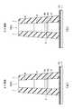
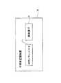
図1は、実施例1に係る半導体装置の製造方法の工程の一例を示す平面図である。また、図2は、図1に示すA−A’線およびB−B’線に沿った断面の例を示す断面図である。また、図3は、図1に続く半導体装置の製造方法の工程の一例を示す平面図である。図4は、図3に示すA−A’線およびB−B’線に沿った断面の例を示す断面図である。また、図4ないし図8は、図3に続く半導体装置の製造方法の工程のA−A’線およびB−B’線に沿った断面の例を示す断面図である。なお、図1においては、簡単のため、素子分離絶縁膜2xは図示していない。 FIG. 1 is a plan view illustrating an example of the steps of the method for manufacturing the semiconductor device according to the first embodiment. FIG. 2 is a cross-sectional view showing an example of a cross section taken along the line A-A ′ and the line B-B ′ shown in FIG. 1. FIG. 3 is a plan view showing an example of the steps of the semiconductor device manufacturing method following FIG. FIG. 4 is a cross-sectional view showing an example of a cross section along the line A-A ′ and the line B-B ′ shown in FIG. 3. 4 to 8 are cross-sectional views showing examples of cross sections taken along the line A-A 'and the line B-B' in the process of the semiconductor device manufacturing method subsequent to FIG. In FIG. 1, the element isolation
先ず、図1および図2に示すように、素子分離用の素子分離絶縁膜2xが選択的に抵抗素子領域に形成された半導体基板1上に、シリコン膜3、このシリコン膜3に対する金属(例えば、タングステン)の拡散を防止するバリアメタル膜4、該金属を含むメタル膜5、ハードマスク膜6の順に積層した積層膜を、形成する。なお、図示しないトランジスタ領域では、半導体基板1の素子分離絶縁膜2xが形成されていない領域にトランジスタが形成される。 First, as shown in FIGS. 1 and 2, on a
さらに、この積層膜を半導体基板1の上面まで選択的にエッチングすることにより、ゲート積層構造膜100aを形成する。そして、ゲート積層構造膜100aの側面にゲート側壁絶縁膜7を形成する。 Further, the laminated film is selectively etched up to the upper surface of the
なお、シリコン膜3は、ここではポリシリコン膜である。しかし、このシリコン膜3は、アモルファスシリコン膜等の導電性を有する他のシリコン膜であってもよい。 Here, the
また、
バリアメタル膜4は、例えば、シリコン膜3上に形成されたチタン(Ti)膜4aと、このチタン膜4a上に形成された窒化チタン(TiN)膜4bと、を含む。なお、バリアメタル膜4は、メタル膜5への拡散を防止するものであれば、WN等の他の材料で構成されていてもよい。Also,
The
また、メタル膜5は、例えば、タングステン(W)膜である。 The
また、ハードマスク膜6は、例えば、シリコン窒化膜である。また、ゲート側壁絶縁膜7は、例えば、シリコン窒化膜、シリコン酸化膜等の絶縁膜により構成される。 The
また、図1に示すように、例えば、シリコン膜3を含むゲート積層構造膜100aは、半導体基板1上に、略ジグザグ状に配置されている。 As shown in FIG. 1, for example, the gate stacked
また、図1に示すように、抵抗素子を形成するための抵抗素子領域1000において、シリコン膜3の両端部は、2つの抵抗用電極(コンタクト)200a、200bに電気的にそれぞれ接続されている。この抵抗用電極200a、200bは、図示しない他の半導体素子等の回路構成に電気的に接続される。 Further, as shown in FIG. 1, in a
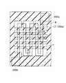
次に、図3および図4に示すように、抵抗素子領域1000において、半導体基板1上に延在するゲート積層構造膜100a上およびゲート側壁絶縁膜7上にレジスト膜8を選択的に形成する。 Next, as shown in FIGS. 3 and 4, a resist
図4(a)の断面図では、ゲート積層構造膜100aおよびゲート側壁絶縁膜7が露出しており、図4(b)の断面図では、ゲート積層構造膜100a上およびゲート側壁絶縁膜7上にレジスト膜8が形成されている。 4A, the gate laminated
なお、ここでは、例えば、抵抗素子領域1000において、レジスト膜8は、半導体基板1上にライン/スペース状に形成されている(図3)。 Here, for example, in the
これにより、後の工程のウエットエッチングにおいて、エッチング液がレジスト膜8の開口部(スペース部)から、エッチングを進めることにより、レジスト膜8が存在する領域の下方にもウェット液が入るようにすることができる。 As a result, in the wet etching in the subsequent process, the etching liquid advances from the opening (space part) of the resist
次に、図5に示すように、レジスト膜8をマスクとして、メタル膜5の表面が露出するように、ゲート側壁絶縁膜7の上部およびハードマスク膜6を、例えば、ドライエッチングにより選択的に除去する。 Next, as shown in FIG. 5, using the resist
なお、本実施例では、ゲート側壁絶縁膜7のエッチングにおいて、少なくともシリコン膜3の表面が露出しないように、ゲート側壁絶縁膜7をエチングする。 In this embodiment, in etching the gate sidewall insulating
これにより、シリコン膜3の加工は、ゲート積層構造膜100aの形成時の加工のみとなる。後の工程のメタル除去は高選択性のウエットエッチングによるため、シリコン膜3の加工によるサイズばらつきを抑制することができる。すなわち、シリコン膜3の加工による抵抗素子の特性のばらつきを低減することができる。 As a result, the
次に、図6に示すように、抵抗素子領域1000において、メタル膜5の露出した表面から、ハードマスク膜6が残存するシリコン膜3上の領域xまで、メタル膜5およびメタル膜5に繋がるバリアメタル膜4を、ウエットエッチングにより除去する。なお、該ウエットエッチングのエッチング液は、例えば、硫酸過水が選択される。 Next, as shown in FIG. 6, in the
これにより、抵抗素子領域1000において、シリコン膜3の上面3aからメタル膜5およびバリアメタル膜4が除去される。したがって、ポリメタルゲートプロセスで形成された半導体素子において、抵抗値が高いポリシリコン抵抗を形成することができる。すなわち、回路面積の増加を抑えつつ、高抵抗な抵抗素子を形成することができる。 Thereby, the
また、上述のように、高選択性のウエットエッチングによりメタル膜5およびバリアメタル膜4を選択的に除去するため、シリコン膜3の加工によるサイズばらつきを抑制することができる。すなわち、シリコン膜3の加工による抵抗素子の特性のばらつきを低減することができる。 Moreover, since the
次に、ウエットエッチングの後、レジスト膜8を除去する。そして、図7に示すように、レジスト膜8を除去した後、例えば、スピンコート法等により、メタル膜5およびバリアメタル膜4を除去した部分を埋め込み絶縁膜(PMD:Pre−Metal Dielectric)9aで埋めるとともに、残存するハードマスク膜6の上面6aよりも上の高さまで、埋め込み絶縁膜9bを成膜する。 Next, after the wet etching, the resist
なお、この埋め込み絶縁膜9a、9bは、例えば、シリコン酸化膜である。 The buried insulating
次に、図8に示すように、埋め込み絶縁膜9bの上部を、残存するハードマスク膜6をストッパとして、CMP法により平坦化する。すなわち、CMP法よる平坦化時に、メタル膜5上のハードマスク膜6が残存しているので、既述の比較例のようなディッシングの発生を抑制することができる。 Next, as shown in FIG. 8, the upper portion of the buried insulating
以上のような本実施例による半導体装置の製造方法により形成される抵抗素子は、半導体基板1と、この半導体基板1上に、シリコン膜3、埋め込み絶縁膜9a、ハードマスク膜6の順に積層され、半導体基板1上に延在する積層構造膜と、この積層構造膜の側面に形成されたゲート側壁絶縁膜7と、半導体基板1上に、ハードマスクの上面の高さまで形成された埋め込み絶縁膜9bと、を備える。そして、該抵抗素子において、埋め込み絶縁膜9aと埋め込み絶縁膜9bとが繋がるように、ゲート側壁絶縁膜7の一部とハードマスク膜6の一部が選択的に除去されており、埋め込み絶縁膜9aと埋め込み絶縁膜9bとは同じ材質で構成され、シリコン膜3の両端部は、2つの抵抗用電極200a、200bに電気的にそれぞれ接続されている。 The resistance element formed by the semiconductor device manufacturing method according to the present embodiment as described above is laminated on the
既述のように、本実施例1による半導体装置の製造方法により形成された上記抵抗素子は、CMP法による平坦化時に、ディッシングの発生が抑制されており、多層構造に適している。 As described above, the resistance element formed by the method of manufacturing a semiconductor device according to the first embodiment is suppressed in the occurrence of dishing when planarized by the CMP method, and is suitable for a multilayer structure.
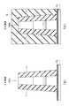
ここで、図9は、実施例1に係る半導体装置の製造方法の工程の他の例を示す平面図である。なお、図9において、図1の符号と同じ符号は、図1と同様の構成を示す。 FIG. 9 is a plan view illustrating another example of the process of the method for manufacturing the semiconductor device according to the first embodiment. 9, the same reference numerals as those in FIG. 1 indicate the same configurations as those in FIG. 1.
図9に示すように、例えば、抵抗素子領域1000において、レジスト膜8は、半導体基板1上にスリット状に形成されるようにしてもよい。 As shown in FIG. 9, for example, in the
この場合も、後の工程のウエットエッチングにおいて、エッチング液がレジスト膜8の開口部(スペース部)から、エッチングを進めることにより、レジスト膜8が存在する領域の下方にもウェット液が入るようにすることができる。 Also in this case, in the wet etching in the subsequent process, the etching liquid advances from the opening (space part) of the resist
以上のように、本実施例1に係る半導体装置の製造方法によれば、回路面積の増大を抑えつつ、ポリシリコン抵抗を用いて所望の特性を有する抵抗素子を形成することができる。 As described above, according to the method for manufacturing a semiconductor device according to the first embodiment, it is possible to form a resistance element having desired characteristics using a polysilicon resistor while suppressing an increase in circuit area.
既述の実施例1では、抵抗素子を形成する抵抗素子領域に注目して説明した。実施例1では、抵抗素子領域において、シリコン膜上にバリアメタル膜が直接形成されている。したがって、シリコン膜とのバリアメタル膜との界面にシリサイド膜が形成される。このシリサイド膜はウエットエッチングによる除去がしにくく、シリサイド膜が残存し得る。これにより、抵抗素子の抵抗値の管理が困難になり得る。 In the above-described first embodiment, the description has been given focusing on the resistance element region in which the resistance element is formed. In Example 1, the barrier metal film is directly formed on the silicon film in the resistance element region. Therefore, a silicide film is formed at the interface between the silicon film and the barrier metal film. This silicide film is difficult to remove by wet etching, and the silicide film may remain. This can make it difficult to manage the resistance value of the resistance element.
そこで、本実施例2では、抵抗素子領域で該シリサイド膜が発生しないようにする方法の一例について説明する。なお、本実施例2においては、この抵抗素子領域と、MOSトランジスタが形成されるトランジスタ領域と、の2つの領域に注目して説明する。 In the second embodiment, an example of a method for preventing the silicide film from being generated in the resistance element region will be described. In the second embodiment, description will be made by paying attention to two regions, that is, the resistance element region and the transistor region in which the MOS transistor is formed.
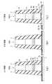
ここで、図10は、実施例2に係る半導体装置の製造方法の工程の一例を示す平面図である。また、図11ないし図14は、実施例2に係る半導体装置の製造方法の工程の、図10に示すA−A’線、B−B’線およびC−C’線に沿った断面の例を示す断面図である。また図15は、図14に続く、実施例2に係る半導体装置の製造方法の工程の一例を示す平面図である。また、図16ないし図20は、実施例2に係る半導体装置の製造方法の工程の、図15に示すA−A’線、B−B’線およびC−C’線に沿った断面の例を示す断面図である。なお、図10ないし図20において、図1ないし図8の符号と同じ符号は、実施例1と同様の構成を示す。 Here, FIG. 10 is a plan view illustrating an example of the steps of the method of manufacturing the semiconductor device according to the second embodiment. 11 to 14 are cross-sectional examples taken along lines AA ′, BB ′, and CC ′ shown in FIG. 10 in the steps of the method for manufacturing the semiconductor device according to the second embodiment. FIG. FIG. 15 is a plan view illustrating an example of the process of the semiconductor device manufacturing method according to the second embodiment, which is subsequent to FIG. FIGS. 16 to 20 are cross-sectional examples taken along lines AA ′, BB ′, and CC ′ shown in FIG. 15 in the steps of the method of manufacturing the semiconductor device according to the second embodiment. FIG. 10 to 20, the same reference numerals as those in FIGS. 1 to 8 indicate the same configurations as those in the first embodiment.
図10では、素子分離絶縁膜2xが選択的に形成された半導体基板1上の抵抗素子領域1000およびMOSトランジスタを形成するためのトランジスタ領域2000にゲート積層構造膜100a、100bとゲート側壁絶縁膜7とが形成された状態を示している。本実施例2では、この抵抗素子領域1000とトランジスタ領域2000とに注目して実施例2に係る半導体装置の製造方法について説明する。 In FIG. 10, the gate stacked
先ず、図11に示すように、抵抗素子領域1000において、素子分離絶縁膜2xが形成された半導体基板1上に、シリコン膜3、保護膜10を形成するとともに、MOSトランジスタを形成するためのトランジスタ領域2000において、素子分離絶縁膜2xが選択的に形成された半導体基板1上に、ゲート絶縁膜2、シリコン膜3、保護膜10を形成する。なお、この保護膜10は、例えば、シリコン酸化膜、シリコン窒化膜等の絶縁膜である。 First, as shown in FIG. 11, in the
なお、抵抗素子領域1000のシリコン膜3に対するイオン注入の条件を、トランジスタ領域2000のシリコン膜3に対するイオン注入の条件とは異なるにしてもよい。すなわち、トランジスタ領域2000におけるシリコン膜3の不純物濃度は、抵抗素子領域1000におけるシリコン膜3の不純物濃度とは異なるようにしてもよい。 Note that the ion implantation conditions for the
これにより、抵抗素子領域1000に形成される抵抗素子の抵抗値を、トランジスタの製造条件とは独立して制御・設計することができる。 Thus, the resistance value of the resistance element formed in the
次に、図12に示すように、抵抗素子領域1000において、保護膜10上にレジスト膜11を形成し、このレジスト膜11をマスクとして、トランジスタ領域2000のシリコン膜3上の保護膜10を除去する。このように、ポリメタルゲートとして用いたい箇所は保護膜を除去する。そして、抵抗素子領域1000において、抵抗素子として用いたい箇所は保護膜10が存在するためバリアメタル・シリコン界面にシリサイドは形成されない。 Next, as shown in FIG. 12, a resist
次に、図13に示すように、バリアメタル膜4、該金属を含むメタル膜5、ハードマスク膜6の順に積層する。 Next, as shown in FIG. 13, a
すなわち、抵抗素子領域1000において、該積層膜の形成の際、シリコン膜3上に、シリサイドの形成を抑制するための保護膜10を形成し、この保護膜10上にバリアメタル膜4を形成する。 That is, in the
次に、図14に示すように、得られた積層膜を半導体基板1の上面まで選択的にエッチングすることにより、ゲート積層構造膜100a1、100bを形成する。そして、ゲート積層構造膜100a1、100bの側面にゲート側壁絶縁膜7を形成するとともに、トランジスタ領域2000においては、イオン注入により、トランジスタ領域のソース・ドレイン領域1aを形成する。 Next, as shown in FIG. 14, the obtained laminated film is selectively etched to the upper surface of the
このように、抵抗素子領域1000では、シリコン膜3とバリアメタル膜4との間に保護膜10が形成されたゲート積層構造膜100bが形成され(図14(a)、(b))、トランジスタ領域2000では、シリコン膜3とバリアメタル膜4との間に保護膜10が形成されていないゲート積層構造膜100a1が形成される(図14(c))。 Thus, in the
次に、図15および図16に示すように、抵抗素子領域1000において、半導体基板1上に延在するゲート積層構造膜100b上およびゲート側壁絶縁膜7上にレジスト膜8を選択的に形成する(図16(a)、(b))とともに、トランジスタ領域2000において、ゲート積層構造膜100a1上およびゲート側壁絶縁膜7上の全てを覆うように、レジスト膜8を形成する(図16(c))。 Next, as shown in FIGS. 15 and 16, in the
なお、ここでは、例えば、抵抗素子領域1000において、レジスト膜8は、半導体基板1上にライン/スペース状に形成されている(図15)。 Here, for example, in the
これにより、実施例1と同様に、後の工程のウエットエッチングにおいて、エッチング液がレジスト膜8の開口部(スペース部)から、エッチングを進めることにより、レジスト膜8が存在する領域の下方にもウェット液が入るようにすることができる。 Thus, in the same way as in Example 1, in the subsequent wet etching, the etching solution advances the etching from the opening (space part) of the resist
次に、図17に示すように、実施例1と同様に、レジスト膜8をマスクとして、メタル膜5の表面が露出するように、ゲート側壁絶縁膜7の上部およびハードマスク膜6を、例えば、ドライエッチングにより選択的に除去する。 Next, as shown in FIG. 17, as in Example 1, the upper portion of the gate sidewall insulating
また、本実施例1と同様に、ゲート側壁絶縁膜7のエッチングにおいて、少なくともシリコン膜3の表面が露出しないように、ゲート側壁絶縁膜7をエチングする。 Similarly to the first embodiment, in the etching of the gate sidewall insulating
これにより、シリコン膜3の加工は、ゲート積層構造膜100bの形成時の加工のみとなる。後の工程のメタル除去は高選択性のウエットエッチングによるため、シリコン膜3の加工によるサイズばらつきを抑制することができる。すなわち、シリコン膜3の加工による抵抗素子の特性のばらつきを低減することができる。 As a result, the
次に、図18に示すように、抵抗素子領域1000において、メタル膜5の露出した表面から、ハードマスク膜6が残存するシリコン膜3上の領域xまで、メタル膜5およびメタル膜5に繋がるバリアメタル膜4を、ウエットエッチングにより除去する。なお、実施例1と同様に、該ウエットエッチングのエッチング液は、例えば、硫酸過水が選択される。 Next, as shown in FIG. 18, in the
このとき、既述のようにシリコン酸化膜等からなる保護膜10は、エッチングされない。 At this time, as described above, the
なお、トランジスタ領域2000においては、ハードマスク膜6およびゲート側壁絶縁膜7によりメタル膜5およびバリアメタル膜4は被覆されたままであるので、メタル膜5およびバリアメタル膜4はウエットエッチングされない。 In
これにより、抵抗素子領域1000において、シリコン膜3の上面3aからメタル膜5およびバリアメタル膜4が除去される。したがって、ポリメタルゲートプロセスで形成された半導体素子において、抵抗値が高いポリシリコン抵抗を形成することができる。すなわち、回路面積の増加を抑えつつ、高抵抗な抵抗素子を形成することができる。 Thereby, the
また、上述のように、高選択性のウエットエッチングによりメタル膜5およびバリアメタル膜4を選択的に除去するため、シリコン膜3の加工によるサイズばらつきを抑制することができる。すなわち、シリコン膜3の加工による抵抗素子の特性のばらつきを低減することができる。 Moreover, since the
さらに、バリアメタル膜4とシリコン膜3との間に介在する保護膜10により抵抗素子の抵抗値に影響を与えるシリサイド膜の発生を抑えられている。すなわち、抵抗値の管理が容易になる。 Furthermore, the generation of a silicide film that affects the resistance value of the resistance element is suppressed by the
次に、ウエットエッチングの後、レジスト膜8を除去する。そして、図19に示すように、レジスト膜8を除去した後、例えば、スピンコート法等により、メタル膜5およびバリアメタル膜4を除去した部分を埋め込み絶縁膜9aで埋めるとともに、残存するハードマスク膜6の上面6aよりも上の高さまで、埋め込み絶縁膜9bを成膜する。 Next, after the wet etching, the resist
次に、図20に示すように、埋め込み絶縁膜9bの上部を、残存するハードマスク膜6をストッパとして、CMP法により平坦化する。すなわち、実施例1と同様に、CMP法よる平坦化時に、メタル膜5上のハードマスク膜6が残存しているので、既述の比較例のようなディッシングの発生を抑制することができる。 Next, as shown in FIG. 20, the upper portion of the buried insulating
以上のような本実施例による半導体装置の製造方法により形成される抵抗素子は、において、素子分離絶縁膜2xが形成された半導体基板1と、この半導体基板1上に、シリコン膜3、保護膜10、埋め込み絶縁膜9a、ハードマスク膜6の順に積層され、半導体基板1上に延在する積層構造膜と、この積層構造膜の側面に形成されたゲート側壁絶縁膜7と、半導体基板1上に、ハードマスクの上面の高さまで形成された埋め込み絶縁膜9bと、を備える。そして、該抵抗素子において、埋め込み絶縁膜9aと埋め込み絶縁膜9bとが繋がるように、ゲート側壁絶縁膜7の一部とハードマスク膜6の一部が選択的に除去されており、埋め込み絶縁膜9aと埋め込み絶縁膜9bとは同じ材質で構成され、シリコン膜3の両端部は、2つの抵抗用電極200a、200bに電気的にそれぞれ接続されている。 In the resistance element formed by the semiconductor device manufacturing method according to the present embodiment as described above, the
実施例1と同様に、本実施例2による半導体装置の製造方法により形成された上記抵抗素子は、CMP法による平坦化時に、ディッシングの発生が抑制されており、多層構造に適している。 Similar to the first embodiment, the resistance element formed by the method of manufacturing a semiconductor device according to the second embodiment suppresses the occurrence of dishing during planarization by the CMP method, and is suitable for a multilayer structure.
以上のように、本実施例2に係る半導体装置の製造方法によれば、面積の増大を抑えつつ、ポリシリコン抵抗を用いて所望の特性を有する抵抗素子を形成することができる。 As described above, according to the method for manufacturing a semiconductor device according to the second embodiment, it is possible to form a resistance element having desired characteristics using a polysilicon resistor while suppressing an increase in area.
本実施例3では、既述の実施例1、2の半導体装置の製造方法で形成された半導体装置をMRAM等の半導体記憶装置に適用した構成の一例について説明する。 In the third embodiment, an example of a configuration in which the semiconductor device formed by the semiconductor device manufacturing method of the first and second embodiments described above is applied to a semiconductor memory device such as an MRAM will be described.
ここで、図21は、実施例3に係る半導体記憶装置の構成の一例を示すブロック図である。 FIG. 21 is a block diagram illustrating an example of the configuration of the semiconductor memory device according to the third embodiment.
半導体記憶装置(例えば、MRAM)Mは、既述の実施例1、2により半導体基板1上に形成された抵抗素子Rと、半導体基板1上に形成されたMOSトランジスタTrと、を備える。 The semiconductor memory device (for example, MRAM) M includes a resistance element R formed on the
このような半導体記憶装置Mは、既述のように、MOSトランジスタTrの形成とともに抵抗素子Rが形成されるものであり、また、抵抗素子Rの回路面積の縮小を図ることができ、さらに、CMP法による平坦化時に、ディッシングの発生が抑制されるため、多層化に適している。 As described above, such a semiconductor memory device M is formed with the resistance element R together with the formation of the MOS transistor Tr. Further, the circuit area of the resistance element R can be reduced. Since the occurrence of dishing is suppressed during planarization by the CMP method, it is suitable for multilayering.
なお、実施形態は例示であり、発明の範囲はそれらに限定されない。 In addition, embodiment is an illustration and the range of invention is not limited to them.
1 半導体基板
2x 素子分離絶縁膜
2 ゲート絶縁膜
3 シリコン膜
4 バリアメタル膜
5 メタル膜
6 ハードマスク膜
7 ゲート側壁
100a ゲート積層構造
1000 抵抗素子領域DESCRIPTION OF
Claims (8)
Translated fromJapanese素子分離絶縁膜が選択的に形成された半導体基板上に、シリコン膜、前記シリコン膜に対する金属の拡散を防止するバリアメタル膜、前記金属を含むメタル膜、ハードマスク膜の順に積層した積層膜を、形成し、
前記積層膜を半導体基板の上面まで選択的にエッチングすることにより、ゲート積層構造膜を形成し、
前記ゲート積層構造膜の側面にゲート側壁絶縁膜を形成し、
抵抗素子を形成するための抵抗素子領域において、前記半導体基板上に延在する前記ゲート積層構造膜上および前記ゲート側壁絶縁膜上にレジスト膜を選択的に形成し、
前記レジスト膜をマスクとして、前記メタル膜の表面が露出するように、前記ゲート側壁絶縁膜の上部および前記ハードマスク膜を、エッチングにより選択的に除去し、
前記抵抗素子領域において、前記メタル膜の露出した表面から、前記ハードマスク膜が残存する前記シリコン膜上の領域まで、前記メタル膜および前記メタル膜に繋がる前記バリアメタル膜を、ウエットエッチングにより除去し、
前記ウエットエッチングの後、前記レジスト膜を除去し、
前記レジスト膜を除去した後、前記メタル膜および前記バリアメタル膜を除去した部分を埋めるとともに、残存する前記ハードマスク膜の上面よりも上の高さまで、埋め込み絶縁膜を成膜し、
前記埋め込み絶縁膜の上部を、残存する前記ハードマスク膜をストッパとして、CMP法により平坦化する
ことを特徴とする半導体装置の製造方法。A method of manufacturing a semiconductor device in which a resistance element is formed from a silicon film used for a gate stacked structure film of a MOS transistor,
A laminated film in which a silicon film, a barrier metal film for preventing metal diffusion to the silicon film, a metal film containing the metal, and a hard mask film are laminated on a semiconductor substrate on which an element isolation insulating film is selectively formed. Forming,
By selectively etching the laminated film to the upper surface of the semiconductor substrate, a gate laminated structure film is formed,
Forming a gate sidewall insulating film on a side surface of the gate stacked structure film;
In the resistive element region for forming the resistive element, a resist film is selectively formed on the gate laminated structure film and the gate sidewall insulating film extending on the semiconductor substrate,
Using the resist film as a mask, the upper portion of the gate sidewall insulating film and the hard mask film are selectively removed by etching so that the surface of the metal film is exposed,
In the resistance element region, from the exposed surface of the metal film to the region on the silicon film where the hard mask film remains, the metal film and the barrier metal film connected to the metal film are removed by wet etching. ,
After the wet etching, the resist film is removed,
After removing the resist film, filling the portion from which the metal film and the barrier metal film have been removed, and forming a buried insulating film up to a height above the upper surface of the remaining hard mask film,
The upper portion of the buried insulating film is planarized by CMP using the remaining hard mask film as a stopper.
A method for manufacturing a semiconductor device.
ことを特徴とする請求項1に記載の半導体装置の製造方法。2. The semiconductor device according to claim 1, wherein in the transistor region for forming a MOS transistor, the resist film is formed so as to cover all over the gate stacked structure film and the gate sidewall insulating film. Production method.
ことを特徴とする請求項2に記載の半導体装置の製造方法。In the resistance element region, when forming the laminated film, a protective film for suppressing the formation of silicide is formed on the silicon film, and the barrier metal film is formed on the protective film. A method for manufacturing a semiconductor device according to claim 2.
ことを特徴とする請求項2または3に記載の半導体装置の製造方法。4. The method of manufacturing a semiconductor device according to claim 2, wherein an impurity concentration of the silicon film in the transistor region is different from an impurity concentration of the silicon film in the resistance element region. 5.
ことを特徴とする請求項1ないし4のいずれか一項に記載の半導体装置の製造方法。The method of manufacturing a semiconductor device according to claim 1, wherein the resist film is formed in a slit shape on the semiconductor substrate in the resistance element region.
ことを特徴とする請求項1ないし5のいずれか一項に記載の半導体装置の製造方法。6. The semiconductor device according to claim 1, wherein in etching the gate sidewall insulating film, the gate sidewall insulating film is etched so that at least a surface of the silicon film is not exposed. Production method.
ことを特徴とする請求項1ないし7のいずれか一項に記載の半導体装置の製造方法。8. The semiconductor device manufacture according to claim 1, wherein both ends of the silicon film are electrically connected to two resistance electrodes in the resistance element region, respectively. Method.
Priority Applications (4)
| Application Number | Priority Date | Filing Date | Title |
|---|---|---|---|
| JP2011121905AJP2012248814A (en) | 2011-05-31 | 2011-05-31 | Semiconductor device and manufacturing method of the same |
| PCT/JP2012/055164WO2012164989A1 (en) | 2011-05-31 | 2012-03-01 | Semiconductor device and method for manufacturing same |
| US14/122,567US9048424B2 (en) | 2011-05-31 | 2012-03-01 | Semiconductor device and method of manufacturing the same |
| TW101108929ATWI470700B (en) | 2011-05-31 | 2012-03-15 | Semiconductor device and manufacturing method thereof |
Applications Claiming Priority (1)
| Application Number | Priority Date | Filing Date | Title |
|---|---|---|---|
| JP2011121905AJP2012248814A (en) | 2011-05-31 | 2011-05-31 | Semiconductor device and manufacturing method of the same |
Publications (1)
| Publication Number | Publication Date |
|---|---|
| JP2012248814Atrue JP2012248814A (en) | 2012-12-13 |
Family
ID=47258855
Family Applications (1)
| Application Number | Title | Priority Date | Filing Date |
|---|---|---|---|
| JP2011121905AWithdrawnJP2012248814A (en) | 2011-05-31 | 2011-05-31 | Semiconductor device and manufacturing method of the same |
Country Status (4)
| Country | Link |
|---|---|
| US (1) | US9048424B2 (en) |
| JP (1) | JP2012248814A (en) |
| TW (1) | TWI470700B (en) |
| WO (1) | WO2012164989A1 (en) |
Family Cites Families (50)
| Publication number | Priority date | Publication date | Assignee | Title |
|---|---|---|---|---|
| US4419812A (en)* | 1982-08-23 | 1983-12-13 | Ncr Corporation | Method of fabricating an integrated circuit voltage multiplier containing a parallel plate capacitor |
| US5075250A (en)* | 1991-01-02 | 1991-12-24 | Xerox Corporation | Method of fabricating a monolithic integrated circuit chip for a thermal ink jet printhead |
| US5514612A (en)* | 1993-03-03 | 1996-05-07 | California Micro Devices, Inc. | Method of making a semiconductor device with integrated RC network and schottky diode |
| US6001663A (en)* | 1995-06-07 | 1999-12-14 | Advanced Micro Devices, Inc. | Apparatus for detecting defect sizes in polysilicon and source-drain semiconductor devices and method for making the same |
| JP3415712B2 (en)* | 1995-09-19 | 2003-06-09 | 松下電器産業株式会社 | Semiconductor device and manufacturing method thereof |
| KR100233557B1 (en)* | 1996-06-29 | 1999-12-01 | 김영환 | Polyresistor of analog semiconductor device and manufacturing method thereof |
| JPH10303372A (en)* | 1997-01-31 | 1998-11-13 | Sanyo Electric Co Ltd | Semiconductor integrated circuit and method of manufacturing the same |
| JP4075228B2 (en)* | 1998-09-09 | 2008-04-16 | 株式会社デンソー | Manufacturing method of semiconductor device |
| JP3420104B2 (en)* | 1999-04-21 | 2003-06-23 | 山形日本電気株式会社 | Manufacturing method of resistance element |
| US6497824B1 (en)* | 1999-09-23 | 2002-12-24 | Texas Instruments Incorporated | One mask solution for the integration of the thin film resistor |
| US20010046771A1 (en)* | 1999-09-23 | 2001-11-29 | Philipp Steinmann | Thin film resistor having improved temperature independence and a method of engineering the TCR of the thin film resistor |
| US6548389B2 (en)* | 2000-04-03 | 2003-04-15 | Matsushita Electric Industrial Co., Ltd. | Semiconductor device and method for fabricating the same |
| US7217613B2 (en)* | 2001-04-11 | 2007-05-15 | Newport Fab, Llc | Low cost fabrication of high resistivity resistors |
| JP2003100749A (en)* | 2001-09-20 | 2003-04-04 | Mitsubishi Electric Corp | Semiconductor device and method of manufacturing the same |
| JP2004013920A (en)* | 2002-06-03 | 2004-01-15 | Mitsubishi Electric Corp | Semiconductor storage device |
| JP4004042B2 (en) | 2002-10-16 | 2007-11-07 | Tdk株式会社 | Duplexer |
| JP2004221234A (en) | 2003-01-14 | 2004-08-05 | Matsushita Electric Ind Co Ltd | Semiconductor device and manufacturing method thereof |
| JP2005142346A (en) | 2003-11-06 | 2005-06-02 | Fujitsu Ltd | Unipolar transistor and semiconductor integrated circuit device |
| US7001821B2 (en)* | 2003-11-10 | 2006-02-21 | Texas Instruments Incorporated | Method of forming and using a hardmask for forming ferroelectric capacitors in a semiconductor device |
| US7411208B2 (en)* | 2004-05-27 | 2008-08-12 | Samsung Electronics Co., Ltd. | Phase-change memory device having a barrier layer and manufacturing method |
| WO2006036000A1 (en)* | 2004-09-30 | 2006-04-06 | Ricoh Company, Ltd. | Semiconductor device and fabrication process thereof |
| US7217981B2 (en)* | 2005-01-06 | 2007-05-15 | International Business Machines Corporation | Tunable temperature coefficient of resistance resistors and method of fabricating same |
| KR101058445B1 (en)* | 2005-05-23 | 2011-08-24 | 후지쯔 세미컨덕터 가부시키가이샤 | Semiconductor device |
| KR100672160B1 (en)* | 2005-12-28 | 2007-01-19 | 주식회사 하이닉스반도체 | Register Formation Method of Flash Memory Device |
| JP4854074B2 (en) | 2006-05-31 | 2012-01-11 | セイコーエプソン株式会社 | Manufacturing method of semiconductor device |
| US8124490B2 (en)* | 2006-12-21 | 2012-02-28 | Stats Chippac, Ltd. | Semiconductor device and method of forming passive devices |
| US20090001517A1 (en)* | 2007-06-27 | 2009-01-01 | Leland Scott Swanson | Thermally enhanced semiconductor devices |
| US7749822B2 (en)* | 2007-10-09 | 2010-07-06 | International Business Machines Corporation | Method of forming a resistor and an FET from the metal portion of a MOSFET metal gate stack |
| KR100928504B1 (en)* | 2007-10-19 | 2009-11-26 | 주식회사 동부하이텍 | Semiconductor Device and Manufacturing Method |
| US7749814B2 (en)* | 2008-03-13 | 2010-07-06 | Stats Chippac, Ltd. | Semiconductor device with integrated passive circuit and method of making the same using sacrificial substrate |
| KR100971423B1 (en)* | 2008-04-04 | 2010-07-21 | 주식회사 하이닉스반도체 | Phase change memory device and manufacturing method thereof |
| US8159040B2 (en)* | 2008-05-13 | 2012-04-17 | International Business Machines Corporation | Metal gate integration structure and method including metal fuse, anti-fuse and/or resistor |
| JP2009283497A (en) | 2008-05-19 | 2009-12-03 | Nec Electronics Corp | Semiconductor device and method of manufacturing the same |
| US8269312B2 (en)* | 2008-06-05 | 2012-09-18 | Rohm Co., Ltd. | Semiconductor device with resistive element |
| JP2010021294A (en)* | 2008-07-09 | 2010-01-28 | Nec Electronics Corp | Method for manufacturing semiconductor device |
| TWI446447B (en)* | 2008-10-16 | 2014-07-21 | United Microelectronics Corp | Method for forming a thin film resistor |
| KR101344799B1 (en)* | 2009-03-12 | 2013-12-26 | 후지쯔 가부시끼가이샤 | Semiconductor memory device and method for manufacturing the same |
| JP5358286B2 (en) | 2009-05-19 | 2013-12-04 | ルネサスエレクトロニクス株式会社 | Semiconductor device |
| JP2010283310A (en)* | 2009-06-08 | 2010-12-16 | Panasonic Corp | Semiconductor device and manufacturing method thereof |
| US9000534B2 (en)* | 2009-06-17 | 2015-04-07 | Globalfoundries Inc. | Method for forming and integrating metal gate transistors having self-aligned contacts and related structure |
| US7994576B2 (en)* | 2009-06-22 | 2011-08-09 | United Microelectronics Corp. | Metal gate transistor and resistor and method for fabricating the same |
| US8193900B2 (en)* | 2009-06-24 | 2012-06-05 | United Microelectronics Corp. | Method for fabricating metal gate and polysilicon resistor and related polysilicon resistor structure |
| US8890260B2 (en)* | 2009-09-04 | 2014-11-18 | Taiwan Semiconductor Manufacturing Company, Ltd. | Polysilicon design for replacement gate technology |
| JP2011100910A (en) | 2009-11-09 | 2011-05-19 | Panasonic Corp | Semiconductor device, and method for manufacturing the same |
| US8071437B2 (en)* | 2009-11-19 | 2011-12-06 | United Microelectronics Corp. | Method of fabricating efuse, resistor and transistor |
| US8003461B1 (en)* | 2010-02-04 | 2011-08-23 | United Microelectronics Corp. | Method of fabricating efuse structure, resistor sturcture and transistor sturcture |
| KR20120081288A (en)* | 2011-01-11 | 2012-07-19 | 삼성전자주식회사 | Integrated circuit device having a resistor and method of manufacturing the same |
| US20120292740A1 (en)* | 2011-05-19 | 2012-11-22 | Macronix International Co., Ltd. | High voltage resistance semiconductor device and method of manufacturing a high voltage resistance semiconductor device |
| CN102222763A (en)* | 2011-06-03 | 2011-10-19 | 复旦大学 | RRAM (resistive random access memory) with electric-field enhancement layer and manufacturing method thereof |
| US8927385B2 (en)* | 2012-12-17 | 2015-01-06 | Texas Instruments Incorporated | ZTCR poly resistor in replacement gate flow |
- 2011
- 2011-05-31JPJP2011121905Apatent/JP2012248814A/ennot_activeWithdrawn
- 2012
- 2012-03-01USUS14/122,567patent/US9048424B2/ennot_activeExpired - Fee Related
- 2012-03-01WOPCT/JP2012/055164patent/WO2012164989A1/ennot_activeCeased
- 2012-03-15TWTW101108929Apatent/TWI470700B/ennot_activeIP Right Cessation
Also Published As
| Publication number | Publication date |
|---|---|
| US9048424B2 (en) | 2015-06-02 |
| WO2012164989A1 (en) | 2012-12-06 |
| TW201248738A (en) | 2012-12-01 |
| US20140077145A1 (en) | 2014-03-20 |
| TWI470700B (en) | 2015-01-21 |
Similar Documents
| Publication | Publication Date | Title |
|---|---|---|
| US12272646B2 (en) | Semiconductor memory device | |
| US10475794B1 (en) | Semiconductor device and method for fabricating the same | |
| US9859284B2 (en) | Semiconductor memory device having enlarged cell contact area and method of fabricating the same | |
| US9337089B2 (en) | Method for fabricating a semiconductor device having a bit line contact | |
| TWI713147B (en) | Method for manufacturing semiconductor device | |
| US9018733B1 (en) | Capacitor, storage node of the capacitor, and method of forming the same | |
| KR20130134139A (en) | Semiconductor device and method for using the same | |
| US10008409B2 (en) | Method for fabricating a semiconductor device | |
| US9653600B2 (en) | Semiconductor device and method of fabricating same | |
| CN110890461A (en) | Method for manufacturing embedded magnetic resistance type random access memory | |
| US20150214234A1 (en) | Semiconductor device and method for fabricating the same | |
| JP2012089772A (en) | Method of manufacturing semiconductor device | |
| US10332791B2 (en) | Semiconductor device with a conductive liner | |
| JP2012248814A (en) | Semiconductor device and manufacturing method of the same | |
| KR101067875B1 (en) | Method of manufacturing semiconductor device | |
| US20170352622A1 (en) | Semiconductor device and manufacturing method thereof | |
| KR20100002675A (en) | Method for fabricating the semiconductor device | |
| US20150194382A1 (en) | Interconnect and method of fabricating the same | |
| JP2024061654A (en) | Capacitor structure and semiconductor device including the same | |
| US8809177B2 (en) | Semiconductor device and method for manufacturing the same | |
| US20130341709A1 (en) | Semiconductor device with electrode including intervention film | |
| KR20100079388A (en) | Resistor of nonvolatile memory device and the fabricating method thereof | |
| KR20060038589A (en) | Plug formation method of semiconductor device | |
| KR20080011495A (en) | Wiring structure of semiconductor device and method for forming same |
Legal Events
| Date | Code | Title | Description |
|---|---|---|---|
| A300 | Application deemed to be withdrawn because no request for examination was validly filed | Free format text:JAPANESE INTERMEDIATE CODE: A300 Effective date:20140805 |