JP2012248812A - Manufacturing method of semiconductor optical integrated element - Google Patents
Manufacturing method of semiconductor optical integrated elementDownload PDFInfo
- Publication number
- JP2012248812A JP2012248812AJP2011121863AJP2011121863AJP2012248812AJP 2012248812 AJP2012248812 AJP 2012248812AJP 2011121863 AJP2011121863 AJP 2011121863AJP 2011121863 AJP2011121863 AJP 2011121863AJP 2012248812 AJP2012248812 AJP 2012248812A
- Authority
- JP
- Japan
- Prior art keywords
- optical integrated
- semiconductor optical
- semiconductor
- bonding pad
- integrated device
- Prior art date
- Legal status (The legal status is an assumption and is not a legal conclusion. Google has not performed a legal analysis and makes no representation as to the accuracy of the status listed.)
- Withdrawn
Links
- 239000004065semiconductorSubstances0.000titleclaimsabstractdescription217
- 230000003287optical effectEffects0.000titleclaimsabstractdescription192
- 238000004519manufacturing processMethods0.000titleclaimsabstractdescription26
- 125000006850spacer groupChemical group0.000claimsabstractdescription53
- 238000003491arrayMethods0.000claimsabstractdescription15
- 238000005520cutting processMethods0.000claimsabstractdescription7
- 238000010030laminatingMethods0.000claimsabstract3
- 239000000758substrateSubstances0.000claimsdescription25
- 238000000034methodMethods0.000claimsdescription19
- 239000000463materialSubstances0.000abstractdescription13
- 239000010410layerSubstances0.000description88
- 239000011347resinSubstances0.000description27
- 229920005989resinPolymers0.000description27
- 230000004888barrier functionEffects0.000description14
- 239000012792core layerSubstances0.000description12
- 239000002184metalSubstances0.000description12
- 229910052751metalInorganic materials0.000description12
- 238000007747platingMethods0.000description11
- 230000001681protective effectEffects0.000description10
- 238000005530etchingMethods0.000description8
- 229910004298SiO 2Inorganic materials0.000description3
- 210000001503jointAnatomy0.000description3
- 229910000530Gallium indium arsenideInorganic materials0.000description2
- 229910004541SiNInorganic materials0.000description2
- -1SiO 2Chemical class0.000description2
- UMIVXZPTRXBADB-UHFFFAOYSA-NbenzocyclobuteneChemical compoundC1=CC=C2CCC2=C1UMIVXZPTRXBADB-UHFFFAOYSA-N0.000description2
- 230000015572biosynthetic processEffects0.000description2
- 239000000919ceramicSubstances0.000description2
- 239000013078crystalSubstances0.000description2
- 229920000642polymerPolymers0.000description2
- 150000003377silicon compoundsChemical class0.000description2
- 229910052814silicon oxideInorganic materials0.000description2
- 239000004642PolyimideSubstances0.000description1
- 229910010413TiO 2Inorganic materials0.000description1
- 229910010282TiONInorganic materials0.000description1
- 238000005253claddingMethods0.000description1
- 238000003776cleavage reactionMethods0.000description1
- 238000010586diagramMethods0.000description1
- 238000006073displacement reactionMethods0.000description1
- 238000001312dry etchingMethods0.000description1
- 238000001704evaporationMethods0.000description1
- 229910052737goldInorganic materials0.000description1
- 238000010438heat treatmentMethods0.000description1
- 238000009616inductively coupled plasmaMethods0.000description1
- 238000012986modificationMethods0.000description1
- 230000004048modificationEffects0.000description1
- 239000013307optical fiberSubstances0.000description1
- 238000001020plasma etchingMethods0.000description1
- 229920001721polyimidePolymers0.000description1
- 230000007017scissionEffects0.000description1
- 239000002356single layerSubstances0.000description1
Images


Classifications
- H—ELECTRICITY
- H01—ELECTRIC ELEMENTS
- H01S—DEVICES USING THE PROCESS OF LIGHT AMPLIFICATION BY STIMULATED EMISSION OF RADIATION [LASER] TO AMPLIFY OR GENERATE LIGHT; DEVICES USING STIMULATED EMISSION OF ELECTROMAGNETIC RADIATION IN WAVE RANGES OTHER THAN OPTICAL
- H01S5/00—Semiconductor lasers
- H01S5/02—Structural details or components not essential to laser action
- H01S5/022—Mountings; Housings
- H01S5/0235—Method for mounting laser chips
- H01S5/02355—Fixing laser chips on mounts
- H01S5/0237—Fixing laser chips on mounts by soldering
- B—PERFORMING OPERATIONS; TRANSPORTING
- B82—NANOTECHNOLOGY
- B82Y—SPECIFIC USES OR APPLICATIONS OF NANOSTRUCTURES; MEASUREMENT OR ANALYSIS OF NANOSTRUCTURES; MANUFACTURE OR TREATMENT OF NANOSTRUCTURES
- B82Y20/00—Nanooptics, e.g. quantum optics or photonic crystals
- H—ELECTRICITY
- H01—ELECTRIC ELEMENTS
- H01S—DEVICES USING THE PROCESS OF LIGHT AMPLIFICATION BY STIMULATED EMISSION OF RADIATION [LASER] TO AMPLIFY OR GENERATE LIGHT; DEVICES USING STIMULATED EMISSION OF ELECTROMAGNETIC RADIATION IN WAVE RANGES OTHER THAN OPTICAL
- H01S5/00—Semiconductor lasers
- H01S5/02—Structural details or components not essential to laser action
- H01S5/026—Monolithically integrated components, e.g. waveguides, monitoring photo-detectors, drivers
- H01S5/0265—Intensity modulators
- H—ELECTRICITY
- H01—ELECTRIC ELEMENTS
- H01S—DEVICES USING THE PROCESS OF LIGHT AMPLIFICATION BY STIMULATED EMISSION OF RADIATION [LASER] TO AMPLIFY OR GENERATE LIGHT; DEVICES USING STIMULATED EMISSION OF ELECTROMAGNETIC RADIATION IN WAVE RANGES OTHER THAN OPTICAL
- H01S5/00—Semiconductor lasers
- H01S5/02—Structural details or components not essential to laser action
- H01S5/028—Coatings ; Treatment of the laser facets, e.g. etching, passivation layers or reflecting layers
- H—ELECTRICITY
- H01—ELECTRIC ELEMENTS
- H01S—DEVICES USING THE PROCESS OF LIGHT AMPLIFICATION BY STIMULATED EMISSION OF RADIATION [LASER] TO AMPLIFY OR GENERATE LIGHT; DEVICES USING STIMULATED EMISSION OF ELECTROMAGNETIC RADIATION IN WAVE RANGES OTHER THAN OPTICAL
- H01S5/00—Semiconductor lasers
- H01S5/04—Processes or apparatus for excitation, e.g. pumping, e.g. by electron beams
- H01S5/042—Electrical excitation ; Circuits therefor
- H01S5/0425—Electrodes, e.g. characterised by the structure
- H01S5/04256—Electrodes, e.g. characterised by the structure characterised by the configuration
- H—ELECTRICITY
- H01—ELECTRIC ELEMENTS
- H01S—DEVICES USING THE PROCESS OF LIGHT AMPLIFICATION BY STIMULATED EMISSION OF RADIATION [LASER] TO AMPLIFY OR GENERATE LIGHT; DEVICES USING STIMULATED EMISSION OF ELECTROMAGNETIC RADIATION IN WAVE RANGES OTHER THAN OPTICAL
- H01S2301/00—Functional characteristics
- H01S2301/17—Semiconductor lasers comprising special layers
- H01S2301/176—Specific passivation layers on surfaces other than the emission facet
- H—ELECTRICITY
- H01—ELECTRIC ELEMENTS
- H01S—DEVICES USING THE PROCESS OF LIGHT AMPLIFICATION BY STIMULATED EMISSION OF RADIATION [LASER] TO AMPLIFY OR GENERATE LIGHT; DEVICES USING STIMULATED EMISSION OF ELECTROMAGNETIC RADIATION IN WAVE RANGES OTHER THAN OPTICAL
- H01S5/00—Semiconductor lasers
- H01S5/02—Structural details or components not essential to laser action
- H01S5/0201—Separation of the wafer into individual elements, e.g. by dicing, cleaving, etching or directly during growth
- H01S5/0202—Cleaving
- H—ELECTRICITY
- H01—ELECTRIC ELEMENTS
- H01S—DEVICES USING THE PROCESS OF LIGHT AMPLIFICATION BY STIMULATED EMISSION OF RADIATION [LASER] TO AMPLIFY OR GENERATE LIGHT; DEVICES USING STIMULATED EMISSION OF ELECTROMAGNETIC RADIATION IN WAVE RANGES OTHER THAN OPTICAL
- H01S5/00—Semiconductor lasers
- H01S5/02—Structural details or components not essential to laser action
- H01S5/022—Mountings; Housings
- H01S5/0235—Method for mounting laser chips
- H01S5/02355—Fixing laser chips on mounts
- H01S5/02365—Fixing laser chips on mounts by clamping
- H—ELECTRICITY
- H01—ELECTRIC ELEMENTS
- H01S—DEVICES USING THE PROCESS OF LIGHT AMPLIFICATION BY STIMULATED EMISSION OF RADIATION [LASER] TO AMPLIFY OR GENERATE LIGHT; DEVICES USING STIMULATED EMISSION OF ELECTROMAGNETIC RADIATION IN WAVE RANGES OTHER THAN OPTICAL
- H01S5/00—Semiconductor lasers
- H01S5/04—Processes or apparatus for excitation, e.g. pumping, e.g. by electron beams
- H01S5/042—Electrical excitation ; Circuits therefor
- H01S5/0425—Electrodes, e.g. characterised by the structure
- H01S5/04252—Electrodes, e.g. characterised by the structure characterised by the material
- H—ELECTRICITY
- H01—ELECTRIC ELEMENTS
- H01S—DEVICES USING THE PROCESS OF LIGHT AMPLIFICATION BY STIMULATED EMISSION OF RADIATION [LASER] TO AMPLIFY OR GENERATE LIGHT; DEVICES USING STIMULATED EMISSION OF ELECTROMAGNETIC RADIATION IN WAVE RANGES OTHER THAN OPTICAL
- H01S5/00—Semiconductor lasers
- H01S5/20—Structure or shape of the semiconductor body to guide the optical wave ; Confining structures perpendicular to the optical axis, e.g. index or gain guiding, stripe geometry, broad area lasers, gain tailoring, transverse or lateral reflectors, special cladding structures, MQW barrier reflection layers
- H01S5/22—Structure or shape of the semiconductor body to guide the optical wave ; Confining structures perpendicular to the optical axis, e.g. index or gain guiding, stripe geometry, broad area lasers, gain tailoring, transverse or lateral reflectors, special cladding structures, MQW barrier reflection layers having a ridge or stripe structure
- H01S5/2205—Structure or shape of the semiconductor body to guide the optical wave ; Confining structures perpendicular to the optical axis, e.g. index or gain guiding, stripe geometry, broad area lasers, gain tailoring, transverse or lateral reflectors, special cladding structures, MQW barrier reflection layers having a ridge or stripe structure comprising special burying or current confinement layers
- H01S5/2222—Structure or shape of the semiconductor body to guide the optical wave ; Confining structures perpendicular to the optical axis, e.g. index or gain guiding, stripe geometry, broad area lasers, gain tailoring, transverse or lateral reflectors, special cladding structures, MQW barrier reflection layers having a ridge or stripe structure comprising special burying or current confinement layers having special electric properties
- H01S5/2224—Structure or shape of the semiconductor body to guide the optical wave ; Confining structures perpendicular to the optical axis, e.g. index or gain guiding, stripe geometry, broad area lasers, gain tailoring, transverse or lateral reflectors, special cladding structures, MQW barrier reflection layers having a ridge or stripe structure comprising special burying or current confinement layers having special electric properties semi-insulating semiconductors
- H—ELECTRICITY
- H01—ELECTRIC ELEMENTS
- H01S—DEVICES USING THE PROCESS OF LIGHT AMPLIFICATION BY STIMULATED EMISSION OF RADIATION [LASER] TO AMPLIFY OR GENERATE LIGHT; DEVICES USING STIMULATED EMISSION OF ELECTROMAGNETIC RADIATION IN WAVE RANGES OTHER THAN OPTICAL
- H01S5/00—Semiconductor lasers
- H01S5/20—Structure or shape of the semiconductor body to guide the optical wave ; Confining structures perpendicular to the optical axis, e.g. index or gain guiding, stripe geometry, broad area lasers, gain tailoring, transverse or lateral reflectors, special cladding structures, MQW barrier reflection layers
- H01S5/22—Structure or shape of the semiconductor body to guide the optical wave ; Confining structures perpendicular to the optical axis, e.g. index or gain guiding, stripe geometry, broad area lasers, gain tailoring, transverse or lateral reflectors, special cladding structures, MQW barrier reflection layers having a ridge or stripe structure
- H01S5/227—Buried mesa structure ; Striped active layer
- H01S5/2275—Buried mesa structure ; Striped active layer mesa created by etching
- H—ELECTRICITY
- H01—ELECTRIC ELEMENTS
- H01S—DEVICES USING THE PROCESS OF LIGHT AMPLIFICATION BY STIMULATED EMISSION OF RADIATION [LASER] TO AMPLIFY OR GENERATE LIGHT; DEVICES USING STIMULATED EMISSION OF ELECTROMAGNETIC RADIATION IN WAVE RANGES OTHER THAN OPTICAL
- H01S5/00—Semiconductor lasers
- H01S5/30—Structure or shape of the active region; Materials used for the active region
- H01S5/34—Structure or shape of the active region; Materials used for the active region comprising quantum well or superlattice structures, e.g. single quantum well [SQW] lasers, multiple quantum well [MQW] lasers or graded index separate confinement heterostructure [GRINSCH] lasers
- H01S5/343—Structure or shape of the active region; Materials used for the active region comprising quantum well or superlattice structures, e.g. single quantum well [SQW] lasers, multiple quantum well [MQW] lasers or graded index separate confinement heterostructure [GRINSCH] lasers in AIIIBV compounds, e.g. AlGaAs-laser, InP-based laser
- H01S5/34306—Structure or shape of the active region; Materials used for the active region comprising quantum well or superlattice structures, e.g. single quantum well [SQW] lasers, multiple quantum well [MQW] lasers or graded index separate confinement heterostructure [GRINSCH] lasers in AIIIBV compounds, e.g. AlGaAs-laser, InP-based laser emitting light at a wavelength longer than 1000nm, e.g. InP based 1300 and 1500nm lasers
Landscapes
- Physics & Mathematics (AREA)
- Optics & Photonics (AREA)
- General Physics & Mathematics (AREA)
- Condensed Matter Physics & Semiconductors (AREA)
- Electromagnetism (AREA)
- Chemical & Material Sciences (AREA)
- Engineering & Computer Science (AREA)
- Nanotechnology (AREA)
- Biophysics (AREA)
- Crystallography & Structural Chemistry (AREA)
- Life Sciences & Earth Sciences (AREA)
- Optical Modulation, Optical Deflection, Nonlinear Optics, Optical Demodulation, Optical Logic Elements (AREA)
- Semiconductor Lasers (AREA)
Abstract
Description
Translated fromJapanese本発明は、半導体光集積素子の製造方法に関するものである。 The present invention relates to a method for manufacturing a semiconductor optical integrated device.
従来より、バットジョイント構造を有する半導体光集積素子が知られている。例えば、特許文献1に記載された半導体光集積素子では、半導体レーザ素子と電界吸収型光変調器とが光学的に結合されている。 Conventionally, a semiconductor optical integrated device having a butt joint structure is known. For example, in the semiconductor optical integrated device described in
半導体光集積素子は、例えば半導体レーザ素子といった第1の光半導体素子部と、例えば光変調器といった第2の光半導体素子部とが、共通の基板上にモノリシックに集積された構成を備える。各光半導体素子部は、光導波層を含むストライプメサ構造をそれぞれ有しており、これらのストライプメサ構造は、いわゆるバットジョイント法によって形成され、相互に結合している。多くの場合、これらのストライプメサ構造は、例えば半絶縁性半導体や樹脂等によって埋め込まれる。また、これらのストライプメサ構造上にはそれぞれ電極が形成され、更に、これらの電極に電力を供給するためのワイヤがボンディングされるボンディングパッドが、これらの電極の近傍にそれぞれ形成される。そして、これらのボンディングパッドとその下方の半導体部分との間には、浮遊容量を低減するために樹脂層が設けられることが望ましい。このような構成を備える半導体光集積素子の端面に反射膜や反射防止膜を形成する際には、複数の半導体光集積素子と複数のスペーサーとを基板の厚さ方向に交互に積層して固定したのち、端面に膜を形成する。 The semiconductor optical integrated device has a configuration in which a first optical semiconductor element unit such as a semiconductor laser element and a second optical semiconductor element unit such as an optical modulator are monolithically integrated on a common substrate. Each optical semiconductor element portion has a stripe mesa structure including an optical waveguide layer, and these stripe mesa structures are formed by a so-called butt joint method and coupled to each other. In many cases, these stripe mesa structures are filled with, for example, a semi-insulating semiconductor or resin. Electrodes are formed on these stripe mesa structures, and further, bonding pads to which wires for supplying power to these electrodes are bonded are formed in the vicinity of these electrodes. A resin layer is preferably provided between these bonding pads and the semiconductor portion below the bonding pads in order to reduce stray capacitance. When forming a reflection film or antireflection film on the end face of a semiconductor optical integrated device having such a configuration, a plurality of semiconductor optical integrated devices and a plurality of spacers are alternately stacked in the thickness direction of the substrate and fixed. After that, a film is formed on the end face.
しかしながら、半導体光集積素子の構造によっては、基板の主面からのボンディングパッドの高さが、各光半導体素子部毎に異なる場合がある。そのような場合、複数の半導体光集積素子と複数のスペーサーとを交互に積層すると、高さが低いボンディングパッドとスペーサーとの間に隙間が生じるので、複数の半導体光集積素子を安定して固定することが難しい。また、このような隙間によってボンディングパッド上に膜材料が回り込み、ボンディングパッドの表面が膜材料に覆われてしまうと、適切なワイヤボンディングが困難になるという問題もある。 However, depending on the structure of the semiconductor optical integrated device, the height of the bonding pad from the main surface of the substrate may be different for each optical semiconductor device portion. In such a case, if a plurality of semiconductor optical integrated devices and a plurality of spacers are alternately stacked, a gap is generated between the bonding pad and the spacer having a low height, so that the plurality of semiconductor optical integrated devices can be stably fixed. Difficult to do. In addition, when the film material flows around the bonding pad by such a gap and the surface of the bonding pad is covered with the film material, there is a problem that appropriate wire bonding becomes difficult.
本発明は、このような問題点に鑑みてなされたものであり、高さが互いに異なる少なくとも2つのボンディングパッドを備える半導体光集積素子の端面に膜を形成する際に、半導体光集積素子を安定して固定でき、且つボンディングパッド上への膜材料の回り込みを低減できる半導体光集積素子の製造方法を提供することを目的とする。 The present invention has been made in view of such problems, and when forming a film on the end face of a semiconductor optical integrated device having at least two bonding pads having different heights, the semiconductor optical integrated device is stabilized. It is an object of the present invention to provide a method of manufacturing a semiconductor optical integrated device that can be fixed in a fixed manner and can reduce the wraparound of the film material on the bonding pad.
上述した課題を解決するために、本発明による半導体光集積素子の製造方法は、第1の方向に延びる光導波軸線を含む第1の光導波層を有する第1のストライプメサ構造、該第1のストライプメサ構造上に設けられた第1の電極、及び、該第1の電極と電気的に接続された第1のボンディングパッドを有する第1の光半導体素子部と、光導波軸線を含む第2の光導波層を有する第2のストライプメサ構造、該第2のストライプメサ構造上に設けられた第2の電極、及び、該第2の電極と電気的に接続された第2のボンディングパッドを有し、第1の光半導体素子部に対して第1の方向に並んで設けられた第2の光半導体素子部とを基板の主面上に備えており、基板の裏面を基準とする第1のボンディングパッドの高さが第2のボンディングパッドの高さより低い半導体光集積素子を製造する方法であって、(1)基板となるウエハ上に、第1の方向及び該第1の方向と交差する第2の方向に並ぶ複数の半導体光集積素子を形成する素子形成工程と、(2)ウエハを第2の方向に沿って切断することにより、二以上の半導体光集積素子をそれぞれ含む棒状の複数の半導体光集積素子アレイを形成する切断工程と、(3)複数の半導体光集積素子アレイと複数のスペーサーとをウエハの厚さ方向に交互に積層して固定する積層工程と、(4)半導体光集積素子アレイの端面上に反射膜又は反射防止膜を形成する膜形成工程とを備え、複数のスペーサーにおける第1のボンディングパッドと対向する部分が、第1のボンディングパッドに向けて突出しており、且つ突出方向に沿って変位可能なように構成されていることを特徴とする。 In order to solve the above-described problem, a method of manufacturing a semiconductor optical integrated device according to the present invention includes a first stripe mesa structure having a first optical waveguide layer including an optical waveguide axis extending in a first direction, A first optical semiconductor element portion having a first electrode provided on the stripe mesa structure, a first bonding pad electrically connected to the first electrode, and an optical waveguide axis. A second stripe mesa structure having two optical waveguide layers; a second electrode provided on the second stripe mesa structure; and a second bonding pad electrically connected to the second electrode On the main surface of the substrate, with the back surface of the substrate as a reference, and the second optical semiconductor element portion arranged in the first direction with respect to the first optical semiconductor element portion The height of the first bonding pad is the second bonding pad A method of manufacturing a semiconductor optical integrated device having a height lower than a height of a semiconductor device, comprising: (1) a plurality of semiconductor lights arranged in a first direction and a second direction intersecting the first direction on a wafer serving as a substrate; An element forming step for forming integrated elements, and (2) cutting to form a plurality of rod-shaped semiconductor optical integrated element arrays each including two or more semiconductor optical integrated elements by cutting the wafer along the second direction. A process, (3) a stacking process for alternately stacking and fixing a plurality of semiconductor optical integrated element arrays and a plurality of spacers in the thickness direction of the wafer, and (4) a reflective film on the end face of the semiconductor optical integrated element array Or a film forming step for forming an antireflection film, and a portion of the plurality of spacers facing the first bonding pad protrudes toward the first bonding pad and can be displaced along the protruding direction. Characterized in that it is configured such.
この半導体光集積素子の製造方法では、基板の裏面を基準とする第1のボンディングパッドの高さが、第2のボンディングパッドの高さより低くなっている。このような半導体光集積素子アレイを通常のスペーサーを用いて固定すると、前述したように第1のボンディングパッドとスペーサーとの間に隙間が生じるので、半導体光集積素子アレイを安定して固定することが難しくなる。また、第1のボンディングパッド上に膜材料が回り込み、第1のボンディングパッドの表面が膜材料に覆われてしまうおそれがある。これに対し、上述した半導体光集積素子の製造方法では、複数のスペーサーにおいて第1のボンディングパッドと対向する部分が、第1のボンディングパッドに向けて突出しており、且つ突出方向に沿って変位可能なように構成されている。これにより、積層工程において複数の半導体光集積素子アレイと複数のスペーサーとを交互に積層したときに、当該部分が第1のボンディングパッドと必ず接触することができ、第1のボンディングパッドとスペーサーとの間に隙間が生じることを防止できる。したがって、上述した半導体光集積素子の製造方法によれば、半導体光集積素子の端面に膜を形成する際に、半導体光集積素子を安定して固定することができ、且つボンディングパッド上への膜材料の回り込みを低減することができる。 In this method of manufacturing a semiconductor optical integrated device, the height of the first bonding pad based on the back surface of the substrate is lower than the height of the second bonding pad. When such a semiconductor optical integrated element array is fixed using a normal spacer, a gap is formed between the first bonding pad and the spacer as described above, so that the semiconductor optical integrated element array can be stably fixed. Becomes difficult. Further, the film material may wrap around the first bonding pad, and the surface of the first bonding pad may be covered with the film material. On the other hand, in the above-described method for manufacturing a semiconductor optical integrated device, portions of the plurality of spacers facing the first bonding pad protrude toward the first bonding pad and can be displaced along the protruding direction. It is configured as follows. As a result, when a plurality of semiconductor optical integrated element arrays and a plurality of spacers are alternately stacked in the stacking step, the portion can always come into contact with the first bonding pad, and the first bonding pad, the spacer, It is possible to prevent a gap from being generated. Therefore, according to the method for manufacturing a semiconductor optical integrated device described above, the semiconductor optical integrated device can be stably fixed when the film is formed on the end face of the semiconductor optical integrated device, and the film on the bonding pad can be obtained. The wraparound of the material can be reduced.
また、上述した半導体光集積素子の製造方法は、複数のスペーサーの上記部分が突出方向に沿って弾性的に変位可能であることを特徴としてもよい。このような構成によって、上記部分の突出の度合いを容易に調整することができ、第1のボンディングパッドとスペーサーとの間に隙間が生じることを好適に防止できる。 Further, the above-described method for manufacturing a semiconductor optical integrated device may be characterized in that the portions of the plurality of spacers can be elastically displaced along the protruding direction. With such a configuration, the degree of protrusion of the portion can be easily adjusted, and a gap can be suitably prevented from being generated between the first bonding pad and the spacer.
また、上述した半導体光集積素子の製造方法は、複数のスペーサーの上記部分の第2の方向の長さが、該第2の方向における半導体光集積素子アレイの一端に位置する半導体光集積素子の第1のボンディングパッドの該方向外側の側面から、該第2の方向における半導体光集積素子アレイの他端に位置する半導体光集積素子の第1のボンディングパッドの該方向外側の側面までの距離よりも長いことを特徴としてもよい。これにより、スペーサーの上記部分と第1のボンディングパッドとの第2の方向における相対位置の許容誤差を確保することができる。 Further, in the above-described method for manufacturing a semiconductor optical integrated device, the length of the plurality of spacers in the second direction is the length of the semiconductor optical integrated device positioned at one end of the semiconductor optical integrated device array in the second direction. The distance from the outer side surface of the first bonding pad in the second direction to the outer side surface of the first bonding pad of the semiconductor optical integrated device located at the other end of the semiconductor optical integrated device array in the second direction. It may be characterized by being long. Thereby, the tolerance of the relative position in the 2nd direction of the said part of a spacer and the 1st bonding pad is securable.
本発明による半導体光集積素子の製造方法によれば、高さが互いに異なる少なくとも2つのボンディングパッドを備える半導体光集積素子の端面に膜を形成する際に、半導体光集積素子を安定して固定でき、且つボンディングパッド上への膜材料の回り込みを低減できる。 According to the semiconductor optical integrated device manufacturing method of the present invention, the semiconductor optical integrated device can be stably fixed when the film is formed on the end face of the semiconductor optical integrated device including at least two bonding pads having different heights. In addition, the wraparound of the film material onto the bonding pad can be reduced.
以下、添付図面を参照しながら本発明による半導体光集積素子の製造方法の実施の形態を詳細に説明する。なお、図面の説明において同一の要素には同一の符号を付し、重複する説明を省略する。 Embodiments of a method for manufacturing a semiconductor optical integrated device according to the present invention will be described below in detail with reference to the accompanying drawings. In the description of the drawings, the same elements are denoted by the same reference numerals, and redundant description is omitted.
まず、本実施形態に係る半導体光集積素子の製造方法によって製造される半導体光集積素子の構成について説明する。この半導体光集積素子は、主に光ファイバ通信システムに使用されるモノリシック集積型の半導体光導波路素子である。図1は、この半導体光集積素子10の構成を示す平面図である。図2は、図1に示された半導体光集積素子10のII−II線に沿った断面図である。図3(a)は、図1に示された半導体光集積素子10のIIIa−IIIa線に沿った断面図である。図3(b)は、図1に示された半導体光集積素子10のIIIb−IIIb線に沿った断面図である。なお、図1〜図3には、理解の容易のためにXYZ直交座標系が併せて示されている。 First, the configuration of a semiconductor optical integrated device manufactured by the method for manufacturing a semiconductor optical integrated device according to the present embodiment will be described. This semiconductor optical integrated device is a monolithic integrated semiconductor optical waveguide device mainly used in an optical fiber communication system. FIG. 1 is a plan view showing the configuration of the semiconductor optical integrated
図1に示されるように、半導体光集積素子10は、基板20と、例えば半導体レーザ素子といった第1の光半導体素子部30と、例えば半導体光変調素子といった第2の光半導体素子部50とを備えている。基板20は、例えばn型InPといった導電性の半導体からなり、主面20a及び裏面20bを有している。第1の光半導体素子部30は半導体レーザ素子としての構造を有しており、第2の光半導体素子部50は光変調素子としての構造を有している。第1及び第2の光半導体素子部30,50は、X軸方向(第1の方向)に並んで基板20の主面20a上に設けられている。 As shown in FIG. 1, the semiconductor optical
図3(a)に示されるように、第1の光半導体素子部30は、基板20の主面20a上に結晶成長したn型半導体領域31と、n型半導体領域31上に結晶成長した活性層(第1の光導波層)32と、活性層32上に結晶成長したp型半導体領域33とを有している。n型半導体領域31は、例えばn型InPを主に含んで構成され、活性層32を導波する光に対して下部クラッドとして機能する。p型半導体領域33は、例えばp型InPを主に含んで構成され、活性層32を導波する光に対して上部クラッドとして機能する。また、p型半導体領域33には、後述する電極40とのオーミック接触を行うためのp型コンタクト層が含まれている。p型コンタクト層は、例えば高濃度のp型InGaAsからなる。 As shown in FIG. 3A, the first optical
活性層32は、レーザ光となる光を発生するとともに、この光を導波する層である。活性層32は、例えばバンドギャップ波長1.33μmの単一InGaAsP層から成ってもよい。或いは、活性層32は、バンドギャップ波長1.54μmのInGaAsP井戸層と、バンドギャップ波長1.25μmのInGaAsPバリア層とが交互に積層された多重量子井戸構造(MQW)から成ってもよい。 The
n型半導体領域31、活性層32、及びp型半導体領域33は、図3(a)に示されるように、光導波路となる部分を残して他の部分が除去されたストライプメサ構造34(第1のストライプメサ構造)を構成している。このストライプメサ構造34は、X軸方向に延びる一対の側面34a及び34bを有している。ストライプメサ構造34に含まれる活性層32は、X軸方向に延びる光導波軸線L(図1を参照)の一部を包含する。主面20a上において、このストライプメサ構造34の両側には埋込半導体領域35,36が形成されている。埋込半導体領域35,36は、例えば主面20a上に結晶成長したFeドープInPといった半絶縁性半導体によって構成されており、ストライプメサ構造34の側面34a,34bをそれぞれ埋め込んでいる。なお、埋込半導体領域35,36上からその外側の主面20a上にわたって、絶縁保護膜37が形成されている。絶縁保護膜37は、例えばSiO2、SiON、或いはSiNといったシリコン化合物によって構成されている。As shown in FIG. 3A, the n-
更に、埋込半導体領域35,36それぞれの外側(ストライプメサ構造34に接する側の反対側)における主面20a上には、樹脂層38が設けられている。樹脂層38は、例えばベンゾシクロブテン(BCB)、ポリイミド、或いはALポリマー(旭硝子株式会社製)等のポリマーによって構成されている。樹脂層38の厚さは、埋込半導体領域35,36と絶縁保護膜37との合計厚さにほぼ等しく、埋込半導体領域35,36上の絶縁保護膜37表面から樹脂層38の表面にかけて、ほぼ平坦となっている。なお、一実施例では、樹脂層38の厚さは2μm〜3μmである。 Further, a
ストライプメサ構造34上には絶縁保護膜37の開口が形成されており、該開口を覆うように電極40(第1の電極)が形成されている。電極40は、p型半導体領域33のp型コンタクト層とオーミック接触を成しており、例えば、Au/Zn/Auといった積層構造やPtから成る単一層によって構成される下層と、TiW/AuやTi/Pt/Auといった積層構造によって構成される上層とを含む。図1に示されるように、電極40は、第1の光半導体素子部30のストライプメサ構造34上においてX軸方向に延びた形状を有している。電極40は、基板20の裏面20b上に形成された電極41と協働して、活性層32に駆動電流を供給する。 An opening of the insulating
また、電極40の近傍には、ボンディングパッド42が設けられている。ボンディングパッド42は、樹脂層38上に形成されており、バリア金属層42aとAuメッキ層42bとを含む。バリア金属層42aは、例えばTiW/AuやTi/Pt/Auといった積層構造によって構成され、電極40の上層を形成する際に同時に形成される。なお、バリア金属層42aは、電極40に向けて延びる配線部分42cを含んでおり、該配線部分42cは電極40と接続されている。図2に示されるボンディングパッド42の高さH1(すなわち、裏面20bからAuメッキ層42bの上面までの距離)は、例えば100μm〜200μmである。A
なお、電極40を挟んでボンディングパッド42とは反対側の樹脂層38上には、ダミーのパッド43が形成されている。パッド43は、ボンディングパッド42と同様にバリア金属層43aとAuメッキ層43bとを含んでおり、その平面形状や主面20aからの高さは、ボンディングパッド42と同じである。このようなパッド43が設けられることによって、光導波路部分(ストライプメサ構造34)よりも高い構造物が光導波路部分の左右に設けられることとなるので、後述する積層工程において、スペーサーが光導波路部分に接触することを避け、光導波路部分を好適に保護することができる。また、このように高さが揃った構造物(パッド42,43)が光導波路部分の左右に設けられることにより、後述する積層工程においてスペーサーを積層する際に、光導波路と交差する方向におけるスペーサーと半導体光集積素子アレイとの平行性を保つことができる。また、ボンディングパッド42に対し、光導波路部分に関して左右対称となる構造物であるパッド43が設けられることにより、半導体光集積素子10における機械的応力のバランスを取ることができる。 A
基板20の裏面20b上の全面には、電極41が設けられている。電極41は、基板20とオーミック接触を成しており、例えばAuGe/Auや、AuGe/Ti/Pt/Auといった積層構造を有している。 An
図3(b)に示されるように、第2の光半導体素子部50は、基板20の主面20a上に結晶成長したn型半導体領域51と、n型半導体領域51上に結晶成長したコア層(第2の光導波層)52と、コア層52上に結晶成長したp型半導体領域53とを有している。n型半導体領域51は、例えばn型InPを主に含んで構成され、コア層52を導波する光に対して下部クラッドとして機能する。p型半導体領域53は、例えばp型InPを主に含んで構成され、コア層52を導波する光に対して上部クラッドとして機能する。また、p型半導体領域53には、後述する電極60とのオーミック接触を行うためのp型コンタクト層が含まれている。p型コンタクト層は、例えば高濃度のp型InGaAsからなる。 As shown in FIG. 3B, the second optical
コア層52は、第1の光半導体素子部50において生成されたレーザ光を導波するとともに、このレーザ光を変調する層である。コア層52は、例えばバンドギャップ波長1.33μmの単一InGaAsP層から成ってもよい。或いは、コア層52は、バンドギャップ波長1.48μmのAlGaInAs井戸層と、AlInAsバリア層とが交互に積層された多重量子井戸構造(MQW)から成ってもよい。 The
n型半導体領域51、コア層52、及びp型半導体領域53は、図3(b)に示されるように、光導波路となる部分を残して他の部分が除去されたストライプメサ構造54(第2のストライプメサ構造)を構成している。このストライプメサ構造54は、X軸方向に延びる一対の側面54a及び54bを有している。ストライプメサ構造54に含まれるコア層52は、X軸方向に延びる光導波軸線L(図1を参照)のうち、第1の光半導体素子部30に含まれる部分を除く部分を包含する。主面20a上において、このストライプメサ構造54の両側にはトレンチ(溝)55,56が形成されている。トレンチ55,56は、X軸方向に沿って延びており、そのY軸方向の幅は例えば1μm〜5μmである。また、トレンチ55,56の深さは例えば2μm〜4μmであり、一実施例では基板20の主面20aに達する。なお、トレンチ55,56の内壁面および底面からその外側のp型半導体領域53上にわたって、絶縁保護膜57が形成されている。絶縁保護膜57は、例えばSiO2、SiON、或いはSiNといったシリコン化合物によって構成されている。As shown in FIG. 3B, the n-
ストライプメサ構造54の側面54a及び54bは、樹脂層38によって埋め込まれている。具体的には、樹脂層38は、トレンチ55,56を満たしており、更に、トレンチ55,56の外側のp型半導体領域53上にわたって層状に形成されている。樹脂層38は、前述した第1の光半導体素子部30の樹脂層38と同じ樹脂材料によって構成されており、その厚さは、第1の光半導体素子部30の樹脂層38とほぼ同じである。但し、第2の光半導体素子部50では、第1の光半導体素子部30とは異なり樹脂層38がp型半導体領域53上に形成されているので、裏面20bを基準とする樹脂層38の表面の高さは、第1の光半導体素子部30における樹脂層38の表面の高さより高くなっている。 Side surfaces 54 a and 54 b of the
ストライプメサ構造54上には、樹脂層38の開口38aが形成されており、該開口38aを覆うように電極60(第2の電極)が形成されている。電極60は、p型半導体領域53のp型コンタクト層とオーミック接触を成しており、第1の光半導体素子部30の電極40と同様の層構造を有している。図1に示されるように、電極60は、第2の光半導体素子部50のストライプメサ構造54上においてX軸方向に延びた形状を有している。電極60は、基板20の裏面20b上に形成された電極41と協働して、コア層52に変調電流を供給する。 An
電極60の近傍には、ボンディングパッド62が設けられている。ボンディングパッド62は、樹脂層38上に形成されており、バリア金属層62a、Auメッキ層62b、及び配線部分62cを含む。なお、バリア金属層62a、Auメッキ層62b、及び配線部分62cの構成は、第1の光半導体素子部30のバリア金属層42a、Auメッキ層42b、及び配線部分42cの構成と同様である。また、ボンディングパッド62の厚さは、第1の光半導体素子部30のボンディングパッド42の厚さとほぼ等しい。但し、図2に示されるボンディングパッド62の高さH2(裏面20bからAuメッキ層62bの上面までの距離)は、第1の光半導体素子部30における高さH1より高い。A
なお、電極60を挟んでボンディングパッド62とは反対側の樹脂層38上には、ダミーのパッド63が形成されている。パッド63は、ボンディングパッド62と同様にバリア金属層63aとAuメッキ層63bとを含んでおり、その平面形状や主面20aからの高さは、ボンディングパッド62と同じである。 A
光導波軸線Lと交差する第1の光半導体素子部30の端面30a上には、反射膜44が形成されている。また、光導波軸線Lと交差する第2の光半導体素子部50の端面50a上には、反射膜64が形成されている。反射膜44及び64は、例えばTiON/MgF2やTiO2/SiO2といった積層構造、或いは単一のSiN層によって好適に構成される。A
以上のような構成を備える半導体光集積素子10を製造する方法について説明する。図4は、半導体光集積素子10の製造方法の例を示すフローチャートである。 A method for manufacturing the semiconductor optical
まず、基板20となるウエハ上に、X軸方向(第1の方向)及びY軸方向(第2の方向)に並ぶ複数の半導体光集積素子構造を形成する(素子形成工程S11)。各半導体光集積素子構造の作製過程は以下の通りである。 First, a plurality of semiconductor optical integrated element structures arranged in the X-axis direction (first direction) and the Y-axis direction (second direction) are formed on a wafer to be the substrate 20 (element formation step S11). The manufacturing process of each semiconductor optical integrated device structure is as follows.
まず、基板20となるウエハの主面上に、第1の光半導体素子部30のn型半導体領域31、活性層32、及びp型半導体領域33を順に成長させる。次に、主面上のうち第2の光半導体素子部50となる領域上に形成されたn型半導体領域31、活性層32、及びp型半導体領域33を、エッチングにより除去する。そして、第2の光半導体素子部50のn型半導体領域51、コア層52、及びp型半導体領域53を、主面の該領域上に選択的に成長させる(バットジョイント)。 First, the n-
続いて、第1の光半導体素子部30のn型半導体領域31、活性層32、及びp型半導体領域33をエッチングすることによりストライプメサ構造34を形成し、該エッチングによって露出したウエハの主面上に埋込半導体領域35,36を成長させる。このとき、埋込半導体領域35,36の成長の為に、ストライプメサ構造34の両側の比較的広い領域がエッチングされる。一方、第2の光半導体素子部50のn型半導体領域51、コア層52、及びp型半導体領域53をエッチングしてトレンチ55,56を形成することにより、ストライプメサ構造54を形成する。このように、比較的狭いトレンチ55,56によってストライプメサ構造54を形成するのは、この後の工程においてトレンチ55,56を埋め込む樹脂層38の熱処理時における収縮量を小さくし、更にその後に形成される電極60や配線部分62cの剥がれを回避する為である。なお、ストライプメサ構造34を形成するためのエッチング、及びストライプメサ構造54を形成するためのエッチングとしては、良好な光の伝搬特性を得る為に、垂直性の高い形状および平滑な表面が得られるドライエッチング(例えば、誘導結合プラズマエッチング)が好ましい。 Subsequently, a
そして、絶縁保護膜37,57を形成したのち、ウエハ上の全面に樹脂層38を塗布する。その後、ストライプメサ構造34,54上の樹脂層38及び絶縁保護膜37,57に開口を形成し、電極40,60およびバリア金属層42a,62aを形成したのち、Auメッキ層42b,62bを形成する。樹脂層38に対する開口の形成は、例えばCF4ガスやO2ガス等を用いたプラズマエッチングにより好適に行われる。また、電極40,60およびバリア金属層42a,62aの形成は、例えばリスクオフ法により好適に行われる。Then, after forming insulating
続いて、ウエハをY軸方向に沿って切断することにより、二以上の半導体光集積素子をそれぞれ含む棒状の複数の半導体光集積素子アレイを形成する(切断工程S12)。なお、この工程において、X軸方向と交差する各半導体光集積素子アレイの端面(図1及び図2に示された端面30a及び50a)は、例えば劈開によって形成される。 Subsequently, the wafer is cut along the Y-axis direction to form a plurality of rod-shaped semiconductor optical integrated element arrays each including two or more semiconductor optical integrated elements (cutting step S12). In this step, the end faces (end faces 30a and 50a shown in FIGS. 1 and 2) of each semiconductor optical integrated element array crossing the X-axis direction are formed by, for example, cleavage.
続いて、複数の半導体光集積素子アレイと複数のスペーサーとを、ウエハの厚さ方向(すなわち図1〜図3に示されたZ軸方向)に交互に積層して固定する(積層工程S13)。複数のスペーサーは、例えばSiやセラミック等からなる棒状の部材であり、そのX軸方向の幅は半導体光集積素子アレイとほぼ等しく、Y軸方向の長さは半導体光集積素子アレイよりも長い。続いて、半導体光集積素子アレイの端面上に、図1及び図2に示された反射膜44及び64を形成する(膜形成工程S14)。反射膜44及び64は、例えば膜材料を蒸着することによって好適に形成される。 Subsequently, a plurality of semiconductor optical integrated element arrays and a plurality of spacers are alternately stacked and fixed in the wafer thickness direction (that is, the Z-axis direction shown in FIGS. 1 to 3) (stacking step S13). . The plurality of spacers are rod-shaped members made of, for example, Si or ceramic, and the width in the X-axis direction is substantially equal to that of the semiconductor optical integrated element array, and the length in the Y-axis direction is longer than that of the semiconductor optical integrated element array. Subsequently, the
以上の工程を経た後、半導体光集積素子アレイをチップ状に切断することにより、図1〜図3に示された半導体光集積素子10が完成する。 After the above steps, the semiconductor optical integrated element array shown in FIGS. 1 to 3 is completed by cutting the semiconductor optical integrated element array into chips.
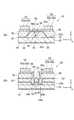
ここで、図5は、本実施形態の積層工程S13及び膜形成工程S14において、半導体光集積素子アレイ70及びスペーサー80が交互に積層された様子を示す断面図であり、光導波方向(X軸方向)に沿った側断面を示している。また、図6は、複数の半導体光集積素子アレイ70のうち、一つの半導体光集積素子アレイ70と、その半導体光集積素子アレイ70に隣接するスペーサー80とを拡大して示す断面図である。 Here, FIG. 5 is a cross-sectional view showing a state in which the semiconductor optical
図5及び図6に示されるように、積層工程S13では、複数の半導体光集積素子アレイ70と複数のスペーサー80とが、ウエハ(基板20)の厚さ方向に交互に積層して固定される。そして、各スペーサー80の一方の側面80aは、該側面80aと対向する半導体光集積素子アレイ70の裏面上に設けられた電極41と接触する。また、他方の側面80bは、該側面80bと対向する半導体光集積素子アレイ70のボンディングパッド62及びパッド63(図1を参照)と接触する。 5 and 6, in the stacking step S13, the plurality of semiconductor optical
ここで、本実施形態の複数のスペーサー80のそれぞれは、可動部81を有している。可動部81は、スペーサー80の側面80bにおいてボンディングパッド42及びパッド43と対向する部分であり、スペーサー80と同じ材料、例えばSiやセラミックからなる。可動部81は、スペーサー80の側面80bから突出しており、また、側面80bに形成された凹部80cに対し、スペーサー80の厚さ方向に変位(摺動)可能な状態で嵌合している。これにより、可動部81は、突出方向(Z軸方向)に沿って変位可能となっている。また、該凹部80c内には例えばバネといった弾性部材82が設けられており、可動部81は、突出方向(Z軸方向)に沿って弾性的に変位することができる。弾性部材82の一端は、スペーサー80の側面80a側に設けられた固定部83によってスペーサー80に固定されている。 Here, each of the plurality of
図5及び図6に示されるように、この可動部81は、複数の半導体光集積素子アレイ70と複数のスペーサー80とが交互に積層された状態において、対向する半導体光集積素子アレイ70のボンディングパッド42及びパッド43と接触する。なお、X軸方向における可動部81の外側の側面81aは、該方向におけるボンディングパッド42の外側の側面42d、及びパッド43の外側の側面(不図示)に対して面一となっていることが好ましい。 As shown in FIGS. 5 and 6, the
図7は、一つの半導体光集積素子アレイ70の平面図であり、図1〜図3に示された半導体光集積素子10に各々相当する複数の構造部分90が、Y軸方向に並んで配置されている。そして、図7には、スペーサー80の可動部81の位置及び大きさを示す仮想線が併せて示されている。同図に示されるように、可動部81はY軸方向(すなわちスペーサ80の長手方向)に延びており、複数の構造部分90のボンディングパッド42及びパッド43に対して一つの可動部81が接触する。なお、Y軸方向における可動部81の長さL1は、図中の距離L2よりも長いことが好ましい。ここで、距離L2は、Y軸方向における半導体光集積素子アレイ70の一端に位置する半導体光集積素子(構造部分90)のボンディングパッド42のY軸方向外側の側面から、Y軸方向における半導体光集積素子アレイ70の他端に位置する半導体光集積素子(構造部分90)のボンディングパッド42のY軸方向外側の側面までの距離である。FIG. 7 is a plan view of one semiconductor optical
再び図5及び図6を参照すると、膜形成工程S14において、反射膜44は、半導体光集積素子アレイ70の端面30a上、ボンディングパッド42の側面42d上、及び可動部81の側面81a上にわたって形成される。また、反射膜64は、半導体光集積素子アレイ70の端面50a上、及びボンディングパッド62の側面62d上にわたって形成される。 Referring again to FIGS. 5 and 6, in the film formation step S <b> 14, the
以上に説明したように、本実施形態による半導体光集積素子の製造方法では、基板20の裏面20bを基準とするボンディングパッド42の高さH1が、ボンディングパッド62の高さH2より低くなっている。これは、ストライプメサ構造34及び54それぞれの両側のエッチング面積が互いに大きく異なるので、樹脂層38を均一に平坦化することが難しいことに起因する。そして、図8に示されるように、このような半導体光集積素子アレイ70を通常のスペーサー100を用いて固定すると、ボンディングパッド42とスペーサー100との間に隙間Aが生じるので、半導体光集積素子アレイ70を安定して固定することが難しくなる。また、ボンディングパッド42上に膜材料が回り込み、ボンディングパッド42の表面が反射膜44によって覆われてしまうおそれがある。このようにボンディングパッド42の表面が反射膜44によって覆われると、ボンディングパッド42へのワイヤボンディングが困難となる。As described above, in the method of manufacturing the semiconductor optical integrated device according to the present embodiment, the height H1 of the
これに対し、本実施形態の製造方法では、複数のスペーサー80においてボンディングパッド42と対向する可動部81が、ボンディングパッド42に向けて突出しており、且つ突出方向(Z軸方向)に変位可能となっている。これにより、積層工程S13において複数の半導体光集積素子アレイ70と複数のスペーサー80とを交互に積層したときに、当該可動部81がボンディングパッド42に向けて突出してボンディングパッド42と接触することができ、ボンディングパッド42とスペーサー80との間に隙間が生じることを防止できる。特に、可動部81が突出方向(Z軸方向)に変位可能であることによって、可動部81の突出の度合いを調整することができ、可動部81がボンディングパッド42に届かない、或いは可動部81が突出し過ぎてスペーサー80が半導体光集積素子アレイ70に対して傾いてしまうといった不都合を防ぐことができる。したがって、本実施形態の製造方法によれば、半導体光集積素子アレイ70の端面30aに反射膜44及び64を形成する際に、半導体光集積素子アレイ70を安定して固定することができ、且つボンディングパッド42上への膜材料の回り込みを低減することができる。 On the other hand, in the manufacturing method of the present embodiment, the
また、本実施形態のように、複数のスペーサー80の可動部81は、ボンディングパッド42に向けて弾性的に突出可能であることが好ましい。このような構成によって、可動部81の突出の度合いを容易に調整することができ、ボンディングパッド42とスペーサー80との間に隙間が生じることを好適に防止できる。 Further, as in the present embodiment, it is preferable that the
また、本実施形態のように、可動部81のY軸方向の長さL1は、図7に示された長さL2よりも長いことが好ましい。これにより、Y軸方向における可動部81とボンディングパッド42との相対位置の許容誤差(すなわち、スペーサー80の長手方向におけるズレの許容量)を確保することができる。Also, as in the present embodiment, Y-axis direction length L1 of the
本発明による半導体光集積素子の製造方法は、上述した実施形態に限られるものではなく、他に様々な変形が可能である。例えば、上述した実施形態では、第1の光半導体素子部として半導体レーザ素子を例示し、第2の光半導体素子部として半導体光変調素子を例示したが、本発明の第1及び第2の光半導体素子部としては、これらに限らず光導波路構造を有する種々の半導体光素子を適用できる。 The method for manufacturing a semiconductor optical integrated device according to the present invention is not limited to the above-described embodiment, and various other modifications are possible. For example, in the above-described embodiment, a semiconductor laser element is exemplified as the first optical semiconductor element portion, and a semiconductor optical modulation element is exemplified as the second optical semiconductor element portion. The semiconductor element portion is not limited to these, and various semiconductor optical elements having an optical waveguide structure can be applied.
また、上述した実施形態では、可動部81は弾性的に変位可能なように構成されているが、可動部81の突き出し量は、例えばスペーサー80の側面80a側に螺合された抑えネジによって調節されてもよい。 In the above-described embodiment, the
また、上述した実施形態では、半導体光集積素子アレイ70の端面30a,50a上に反射膜44,64を成膜しているが、本発明は、半導体光集積素子アレイの端面上に反射防止膜を成膜する場合にも適用可能である。 In the above-described embodiment, the
10…半導体光集積素子、20…基板、30…第1の光半導体素子部、30a,50a…端面、31,51…n型半導体領域、32…活性層、33,53…p型半導体領域、34,54…ストライプメサ構造、34a,34b,54a,54b…側面、35,36…埋込半導体領域、37,57…絶縁保護膜、38…樹脂層、38a…開口、40,60…電極、41…電極、42,62…ボンディングパッド、42a,62a…バリア金属層、42b,62b…メッキ層、42c,62c…配線部分、42d,62d…側面、43,63…パッド、43a,63a…バリア金属層、43b,63b…メッキ層、44,64…反射膜、50…第2の光半導体素子部、52…コア層、55,56…トレンチ、70…半導体光集積素子アレイ、80…スペーサー、80a,80b…側面、80c…凹部、81…可動部、81a…側面、82…弾性部材、83…固定部、L…光導波軸線。 DESCRIPTION OF
Claims (3)
Translated fromJapanese前記基板となるウエハ上に、前記第1の方向及び該第1の方向と交差する第2の方向に並ぶ複数の前記半導体光集積素子を形成する素子形成工程と、
前記ウエハを前記第2の方向に沿って切断することにより、二以上の半導体光集積素子をそれぞれ含む棒状の複数の半導体光集積素子アレイを形成する切断工程と、
前記複数の半導体光集積素子アレイと複数のスペーサーとを前記ウエハの厚さ方向に交互に積層して固定する積層工程と、
前記半導体光集積素子アレイの端面上に反射膜又は反射防止膜を形成する膜形成工程と
を備え、
前記複数のスペーサーにおける前記第1のボンディングパッドと対向する部分が、前記第1のボンディングパッドに向けて突出しており、且つ突出方向に沿って変位可能なように構成されていることを特徴とする、半導体光集積素子の製造方法。A first stripe mesa structure having a first optical waveguide layer including an optical waveguide axis extending in a first direction, a first electrode provided on the first stripe mesa structure, and the first electrode A first optical semiconductor element portion having a first bonding pad electrically connected to the second optical waveguide layer, a second stripe mesa structure having a second optical waveguide layer including the optical waveguide axis, and the second stripe mesa A second electrode provided on the structure; and a second bonding pad electrically connected to the second electrode; and the first direction with respect to the first optical semiconductor element portion. On the main surface of the substrate, and the height of the first bonding pad relative to the back surface of the substrate is the height of the second bonding pad. Method of manufacturing semiconductor optical integrated device lower than height There,
Forming a plurality of the semiconductor optical integrated devices arranged in the first direction and in a second direction intersecting the first direction on the wafer to be the substrate;
A cutting step of cutting the wafer along the second direction to form a plurality of rod-shaped semiconductor optical integrated element arrays each including two or more semiconductor optical integrated elements;
A laminating step of alternately laminating and fixing the plurality of semiconductor optical integrated element arrays and the plurality of spacers in the thickness direction of the wafer;
A film forming step of forming a reflection film or an antireflection film on an end face of the semiconductor optical integrated element array,
A portion of the plurality of spacers facing the first bonding pad protrudes toward the first bonding pad and is configured to be displaceable along the protruding direction. A method for manufacturing a semiconductor optical integrated device.
Priority Applications (2)
| Application Number | Priority Date | Filing Date | Title |
|---|---|---|---|
| JP2011121863AJP2012248812A (en) | 2011-05-31 | 2011-05-31 | Manufacturing method of semiconductor optical integrated element |
| US13/479,567US8563342B2 (en) | 2011-05-31 | 2012-05-24 | Method of making semiconductor optical integrated device by alternately arranging spacers with integrated device arrays |
Applications Claiming Priority (1)
| Application Number | Priority Date | Filing Date | Title |
|---|---|---|---|
| JP2011121863AJP2012248812A (en) | 2011-05-31 | 2011-05-31 | Manufacturing method of semiconductor optical integrated element |
Publications (1)
| Publication Number | Publication Date |
|---|---|
| JP2012248812Atrue JP2012248812A (en) | 2012-12-13 |
Family
ID=47261975
Family Applications (1)
| Application Number | Title | Priority Date | Filing Date |
|---|---|---|---|
| JP2011121863AWithdrawnJP2012248812A (en) | 2011-05-31 | 2011-05-31 | Manufacturing method of semiconductor optical integrated element |
Country Status (2)
| Country | Link |
|---|---|
| US (1) | US8563342B2 (en) |
| JP (1) | JP2012248812A (en) |
Families Citing this family (12)
| Publication number | Priority date | Publication date | Assignee | Title |
|---|---|---|---|---|
| JP2013016648A (en)* | 2011-07-04 | 2013-01-24 | Sumitomo Electric Ind Ltd | Method for manufacturing semiconductor optical integrated element |
| JP5891920B2 (en)* | 2012-04-16 | 2016-03-23 | 三菱電機株式会社 | Modulator integrated laser device |
| DE102014102037A1 (en)* | 2014-02-18 | 2015-08-20 | Osram Opto Semiconductors Gmbh | A semiconductor device and method for applying a coating to a plurality of semiconductor devices |
| TWI556534B (en)* | 2014-06-20 | 2016-11-01 | 錼創科技股份有限公司 | Flip chip type laser diode and flip chip type laser diode package strcture |
| US9787053B2 (en) | 2014-06-20 | 2017-10-10 | PlayNitride Inc. | Laser diode chip and flip chip type laser diode package structure |
| KR102443033B1 (en) | 2015-10-12 | 2022-09-16 | 삼성전자주식회사 | Light emitting device package and lighting apparatus having the same |
| JP2018018950A (en)* | 2016-07-28 | 2018-02-01 | 株式会社沖データ | Semiconductor device, light emitting element array, optical print head, and semiconductor device manufacturing method |
| KR102553630B1 (en) | 2016-08-11 | 2023-07-10 | 삼성전자주식회사 | Led lighting device package and display apparatus using the same |
| US10707145B2 (en) | 2017-09-08 | 2020-07-07 | Kemet Electronics Corporation | High density multi-component packages |
| CN111052347B (en)* | 2017-09-08 | 2024-03-01 | 凯米特电子公司 | High density multi-component and tandem package |
| US10681814B2 (en) | 2017-09-08 | 2020-06-09 | Kemet Electronics Corporation | High density multi-component packages |
| RU2757055C1 (en)* | 2021-04-06 | 2021-10-11 | Федеральное государственное бюджетное учреждение науки Физический институт им. П.Н. Лебедева Российской академии наук (ФИАН) | Two-dimensional array of laser diodes and method for its assembly |
Family Cites Families (105)
| Publication number | Priority date | Publication date | Assignee | Title |
|---|---|---|---|---|
| US3962714A (en)* | 1974-09-19 | 1976-06-08 | Northern Electric Company Limited | Semiconductor optical modulator |
| US5147825A (en)* | 1988-08-26 | 1992-09-15 | Bell Telephone Laboratories, Inc. | Photonic-integrated-circuit fabrication process |
| US5311536A (en)* | 1992-09-22 | 1994-05-10 | Xerox Corporation | Vertically stacked, accurately positioned diode lasers |
| DE4304993A1 (en)* | 1993-02-18 | 1994-08-25 | Sel Alcatel Ag | Process for producing a cascaded optical room switch and cascaded optical room switch produced by this process |
| JP3285426B2 (en)* | 1993-08-04 | 2002-05-27 | 株式会社日立製作所 | Semiconductor optical integrated device and method of manufacturing the same |
| US5522005A (en)* | 1994-02-18 | 1996-05-28 | E-Systems, Inc. | High power waveguide absorption modulator |
| JPH07263655A (en) | 1994-03-18 | 1995-10-13 | Fujitsu Ltd | Optical integrated circuit and manufacturing method thereof |
| JP2762951B2 (en)* | 1995-03-30 | 1998-06-11 | 日本電気株式会社 | Semiconductor optical waveguide and manufacturing method thereof |
| US5898211A (en)* | 1996-04-30 | 1999-04-27 | Cutting Edge Optronics, Inc. | Laser diode package with heat sink |
| JPH1075009A (en)* | 1996-08-30 | 1998-03-17 | Nec Corp | Optical semiconductor device and its manufacture |
| JP2967737B2 (en)* | 1996-12-05 | 1999-10-25 | 日本電気株式会社 | Optical semiconductor device and its manufacturing method |
| US6185238B1 (en)* | 1997-02-21 | 2001-02-06 | Kabushiki Kaisha Toshiba | Nitride compound semiconductor laser and its manufacturing method |
| US6054334A (en)* | 1997-09-12 | 2000-04-25 | Micron Technology, Inc. | Methods and structures for pad reconfiguration to allow intermediate testing during manufacture of an integrated circuit |
| JP3045115B2 (en)* | 1997-09-30 | 2000-05-29 | 日本電気株式会社 | Method for manufacturing optical semiconductor device |
| CA2269872A1 (en)* | 1998-04-23 | 1999-10-23 | Nec Corporation | A method of manufacturing a semiconductor optical waveguide array and an array-structured semiconductor optical device |
| US6597713B2 (en)* | 1998-07-22 | 2003-07-22 | Canon Kabushiki Kaisha | Apparatus with an optical functional device having a special wiring electrode and method for fabricating the same |
| JP3141854B2 (en)* | 1998-09-28 | 2001-03-07 | 日本電気株式会社 | Method for manufacturing optical semiconductor device |
| US6706546B2 (en)* | 1998-10-09 | 2004-03-16 | Fujitsu Limited | Optical reflective structures and method for making |
| JP3907854B2 (en)* | 1998-12-07 | 2007-04-18 | 富士通株式会社 | Semiconductor laser and manufacturing method thereof |
| US7212556B1 (en)* | 1999-02-17 | 2007-05-01 | Matsushita Electric Industrial Co., Ltd. | Semiconductor laser device optical disk apparatus and optical integrated unit |
| US6624000B1 (en)* | 1999-09-02 | 2003-09-23 | Agility Communications, Inc. | Method for making a monolithic wavelength converter assembly |
| CA2381766A1 (en)* | 1999-09-03 | 2001-03-15 | The Regents Of The University Of California | Tunable laser source with integrated optical modulator |
| US6090633A (en)* | 1999-09-22 | 2000-07-18 | International Business Machines Corporation | Multiple-plane pair thin-film structure and process of manufacture |
| JP2001168442A (en)* | 1999-12-07 | 2001-06-22 | Sony Corp | Method of manufacturing semiconductor laser element, installation substrate, and support substrate |
| JP4547765B2 (en)* | 2000-03-30 | 2010-09-22 | 三菱電機株式会社 | Optical modulator, semiconductor laser device with optical modulator, and optical communication device |
| JP4618854B2 (en)* | 2000-08-11 | 2011-01-26 | Okiセミコンダクタ株式会社 | Semiconductor device and manufacturing method thereof |
| JP3440243B2 (en)* | 2000-09-26 | 2003-08-25 | 株式会社アドバンストシステムズジャパン | Spiral contactor |
| US6600224B1 (en)* | 2000-10-31 | 2003-07-29 | International Business Machines Corporation | Thin film attachment to laminate using a dendritic interconnection |
| JP2002174801A (en)* | 2000-12-07 | 2002-06-21 | Oki Electric Ind Co Ltd | Semiconductor optical functional device |
| US20030099273A1 (en)* | 2001-01-09 | 2003-05-29 | Murry Stefan J. | Method and apparatus for coupling a surface-emitting laser to an external device |
| JP3619155B2 (en)* | 2001-01-17 | 2005-02-09 | キヤノン株式会社 | Surface emitting laser device, manufacturing method thereof, and driving method thereof |
| US6944192B2 (en)* | 2001-03-14 | 2005-09-13 | Corning Incorporated | Planar laser |
| US6687268B2 (en)* | 2001-03-26 | 2004-02-03 | Seiko Epson Corporation | Surface emitting laser and photodiode, manufacturing method therefor, and optoelectric integrated circuit using the surface emitting laser and the photodiode |
| WO2003096759A1 (en)* | 2001-03-30 | 2003-11-20 | Santur Corporation | High speed modulation of arrayed lasers |
| US6873638B2 (en)* | 2001-06-29 | 2005-03-29 | 3M Innovative Properties Company | Laser diode chip with waveguide |
| US6730134B2 (en)* | 2001-07-02 | 2004-05-04 | Intercon Systems, Inc. | Interposer assembly |
| JP3654435B2 (en)* | 2001-08-21 | 2005-06-02 | 日本電信電話株式会社 | Semiconductor optical device and manufacturing method thereof |
| JP3643328B2 (en)* | 2001-08-21 | 2005-04-27 | ファナック株式会社 | Two-dimensional LD array light emitting device |
| US6836357B2 (en)* | 2001-10-04 | 2004-12-28 | Gazillion Bits, Inc. | Semiconductor optical amplifier using laser cavity energy to amplify signal and method of fabrication thereof |
| JP4157698B2 (en)* | 2001-11-26 | 2008-10-01 | ユーディナデバイス株式会社 | Semiconductor light receiving element and driving method thereof |
| US7006719B2 (en)* | 2002-03-08 | 2006-02-28 | Infinera Corporation | In-wafer testing of integrated optical components in photonic integrated circuits (PICs) |
| KR100464359B1 (en)* | 2002-03-11 | 2005-01-03 | 삼성전자주식회사 | Tunable laser apparatus |
| DE60215303D1 (en)* | 2002-04-25 | 2006-11-23 | Avalon Photonics Ag | High speed vertical cavity resonator surface emitting laser (VCSEL) with low parasitic capacitance |
| US6768753B2 (en)* | 2002-05-22 | 2004-07-27 | Spectra Physics | Reliable diode laser stack |
| US6836499B2 (en)* | 2002-05-24 | 2004-12-28 | Lucent Technologies Inc. | Optical amplifier for quantum cascade laser |
| JP3873833B2 (en)* | 2002-07-17 | 2007-01-31 | 住友電気工業株式会社 | Heterojunction bipolar transistor and method of manufacturing heterojunction bipolar transistor |
| US7106774B2 (en)* | 2002-08-28 | 2006-09-12 | T-Networks, Inc. | Placing a semiconductor laser electrically in series with a semiconductor optical amplifier |
| JP2004087866A (en)* | 2002-08-28 | 2004-03-18 | Hitachi Ltd | Semiconductor optical device, its mounting body and optical module |
| US6728275B2 (en)* | 2002-09-19 | 2004-04-27 | Trw Inc. | Fault tolerant laser diode package |
| US6901086B2 (en)* | 2002-10-30 | 2005-05-31 | Chian Chiu Li | Stack-type diode laser device |
| JP2004193330A (en)* | 2002-12-11 | 2004-07-08 | Sharp Corp | Monolithic multi-wavelength laser device and its manufacturing method. |
| US7018861B2 (en)* | 2003-01-24 | 2006-03-28 | Agilent Technologies, Inc. | Method of manufacturing integrated semiconductor devices and related devices |
| DE602004024042D1 (en)* | 2003-02-27 | 2009-12-24 | Laserfront Technologies Inc | HEAT EXTINGUISHER, LASER MODULE, LASER DEVICE AND LASER PROCESSING DEVICE |
| KR100964399B1 (en)* | 2003-03-08 | 2010-06-17 | 삼성전자주식회사 | Semiconductor laser diode and semiconductor laser diode assembly using same |
| JP2004273906A (en)* | 2003-03-11 | 2004-09-30 | Mitsubishi Electric Corp | Surface emitting laser device with integrated optical amplifier |
| JP2004273993A (en)* | 2003-03-12 | 2004-09-30 | Hitachi Ltd | Tunable distributed reflection type semiconductor laser device |
| US7597561B2 (en)* | 2003-04-11 | 2009-10-06 | Neoconix, Inc. | Method and system for batch forming spring elements in three dimensions |
| US7114961B2 (en)* | 2003-04-11 | 2006-10-03 | Neoconix, Inc. | Electrical connector on a flexible carrier |
| US7758351B2 (en)* | 2003-04-11 | 2010-07-20 | Neoconix, Inc. | Method and system for batch manufacturing of spring elements |
| JP4037815B2 (en)* | 2003-09-29 | 2008-01-23 | オムロンレーザーフロント株式会社 | Laser diode module, laser device, and laser processing device |
| JP2005311089A (en)* | 2004-04-22 | 2005-11-04 | Fuji Xerox Co Ltd | Vertical resonator type surface-emitting semiconductor laser device |
| KR100640393B1 (en)* | 2004-05-20 | 2006-10-30 | 삼성전자주식회사 | Optical integrated device using inverted mesa structure and its manufacturing method |
| US20060006529A1 (en)* | 2004-07-08 | 2006-01-12 | Min-Jer Lin | Semiconductor package and method for manufacturing the same |
| JP4167209B2 (en)* | 2004-08-12 | 2008-10-15 | 浜松ホトニクス株式会社 | Laser equipment |
| JP4415891B2 (en)* | 2005-03-29 | 2010-02-17 | 住友電気工業株式会社 | Semiconductor optical amplifier |
| JP4755854B2 (en)* | 2005-06-02 | 2011-08-24 | 富士通株式会社 | Semiconductor light receiving device and manufacturing method thereof |
| JP5055717B2 (en)* | 2005-06-20 | 2012-10-24 | 富士ゼロックス株式会社 | Surface emitting semiconductor laser |
| JP4671793B2 (en)* | 2005-07-22 | 2011-04-20 | パナソニック株式会社 | Semiconductor laser device and manufacturing method thereof |
| WO2007029842A1 (en)* | 2005-09-06 | 2007-03-15 | Showa Denko K.K. | Gallium nitride-based compound semiconductor light-emitting device and production method thereof |
| US7873090B2 (en)* | 2005-09-13 | 2011-01-18 | Panasonic Corporation | Surface emitting laser, photodetector and optical communication system using the same |
| US7184207B1 (en)* | 2005-09-27 | 2007-02-27 | Bookham Technology Plc | Semiconductor optical device |
| WO2007044543A2 (en)* | 2005-10-07 | 2007-04-19 | Lee, Michael, J. | Interface for a-si waveguides and iii/v waveguides |
| US20070217467A1 (en)* | 2006-03-20 | 2007-09-20 | Nlight Photonics Corporation | Laser diode package utilizing a laser diode stack |
| US20070116077A1 (en)* | 2005-11-22 | 2007-05-24 | Nlight Photonics Corporation | Vertically displaced stack of multi-mode single emitter laser diodes |
| US20070217468A1 (en)* | 2006-03-20 | 2007-09-20 | Nlight Photonics Corporation | Laser diode package utilizing a laser diode stack |
| JP4892940B2 (en)* | 2005-11-29 | 2012-03-07 | 富士ゼロックス株式会社 | Surface emitting semiconductor laser device and manufacturing method thereof |
| KR100759805B1 (en)* | 2005-12-07 | 2007-09-20 | 한국전자통신연구원 | Optically boosted elctroabsorption duplexer |
| JPWO2007094063A1 (en)* | 2006-02-16 | 2009-07-02 | 富士通株式会社 | Semiconductor optical amplifier |
| EP1830443B1 (en)* | 2006-03-03 | 2016-06-08 | Fraunhofer USA, Inc. | High power diode laser having multiple emitters and method for its production |
| US20070217469A1 (en)* | 2006-03-20 | 2007-09-20 | Nlight Photonics Corporation | Laser diode stack side-pumped solid state laser |
| US20070217470A1 (en)* | 2006-03-20 | 2007-09-20 | Nlight Photonics Corporation | Laser diode stack end-pumped solid state laser |
| JP5197930B2 (en)* | 2006-06-30 | 2013-05-15 | 住友電工デバイス・イノベーション株式会社 | Manufacturing method of semiconductor light receiving element |
| JP4244058B2 (en)* | 2006-09-06 | 2009-03-25 | ソニー株式会社 | Manufacturing method of semiconductor light emitting device |
| JP4928988B2 (en)* | 2007-03-07 | 2012-05-09 | 日本オプネクスト株式会社 | Semiconductor optical device and manufacturing method thereof |
| US7760777B2 (en)* | 2007-04-13 | 2010-07-20 | Finisar Corporation | DBR laser with improved thermal tuning efficiency |
| JP5151231B2 (en)* | 2007-04-23 | 2013-02-27 | 住友電気工業株式会社 | Semiconductor optical device and manufacturing method thereof |
| US7778295B2 (en)* | 2007-05-14 | 2010-08-17 | Finisar Corporation | DBR laser with improved thermal tuning efficiency |
| US7807489B2 (en)* | 2007-05-15 | 2010-10-05 | Sumitomo Electric Industries, Ltd. | Light-emitting device with a protection layer to prevent the inter-diffusion of zinc (Zn) atoms |
| JP4794505B2 (en)* | 2007-06-15 | 2011-10-19 | 富士通株式会社 | Semiconductor optical amplification device, semiconductor optical amplification system, and semiconductor optical integrated device |
| US7811844B2 (en)* | 2007-10-26 | 2010-10-12 | Bae Systems Information And Electronic Systems Integration Inc. | Method for fabricating electronic and photonic devices on a semiconductor substrate |
| JP5250245B2 (en)* | 2007-11-21 | 2013-07-31 | 日本オクラロ株式会社 | Semiconductor laser |
| US7724791B2 (en)* | 2008-01-18 | 2010-05-25 | Northrop Grumman Systems Corporation | Method of manufacturing laser diode packages and arrays |
| US7668223B2 (en)* | 2008-02-22 | 2010-02-23 | Avago Technologies Fiber Ip (Singapore) Pte. Ltd. | Integrated photonic semiconductor devices and methods for making integrated photonic semiconductors devices |
| JP2009246291A (en)* | 2008-03-31 | 2009-10-22 | Furukawa Electric Co Ltd:The | Surface emitting laser element array |
| JP2010010622A (en)* | 2008-06-30 | 2010-01-14 | Sumitomo Electric Ind Ltd | Semiconductor optical device |
| JP5093063B2 (en)* | 2008-11-11 | 2012-12-05 | 住友電気工業株式会社 | Integrated semiconductor optical device and semiconductor optical device |
| JP2010123630A (en)* | 2008-11-17 | 2010-06-03 | Nec Electronics Corp | Semiconductor laser and manufacturing process thereof |
| JP5321886B2 (en)* | 2009-02-06 | 2013-10-23 | ソニー株式会社 | Semiconductor element |
| JP5418887B2 (en)* | 2009-05-27 | 2014-02-19 | 住友電気工業株式会社 | Semiconductor laser device manufacturing method and semiconductor laser device |
| JP2011029595A (en)* | 2009-06-26 | 2011-02-10 | Opnext Japan Inc | Optical module, integrated semiconductor optical device, and method of manufacturing the same |
| JP2011091164A (en)* | 2009-10-21 | 2011-05-06 | Sumitomo Electric Ind Ltd | Semiconductor integrated element |
| JP2011091163A (en)* | 2009-10-21 | 2011-05-06 | Sumitomo Electric Ind Ltd | Semiconductor integrated element |
| KR20110064148A (en)* | 2009-12-07 | 2011-06-15 | 한국전자통신연구원 | Optical element module |
| US8805130B2 (en)* | 2010-03-16 | 2014-08-12 | Cornell University | Semiconductor high-speed integrated electro-optic devices and methods |
| US8390109B2 (en)* | 2011-02-17 | 2013-03-05 | Oracle America, Inc. | Chip package with plank stack of semiconductor dies |
- 2011
- 2011-05-31JPJP2011121863Apatent/JP2012248812A/ennot_activeWithdrawn
- 2012
- 2012-05-24USUS13/479,567patent/US8563342B2/ennot_activeExpired - Fee Related
Also Published As
| Publication number | Publication date |
|---|---|
| US20120309121A1 (en) | 2012-12-06 |
| US8563342B2 (en) | 2013-10-22 |
Similar Documents
| Publication | Publication Date | Title |
|---|---|---|
| JP2012248812A (en) | Manufacturing method of semiconductor optical integrated element | |
| JP4312239B2 (en) | Optical element and manufacturing method thereof | |
| JP5897414B2 (en) | Optical device manufacturing method | |
| US7835418B2 (en) | Optical semiconductor device having diffraction grating disposed on both sides of waveguide and its manufacture method | |
| US20150093121A1 (en) | Optical semiconductor device, optical semiconductor device array, and optical transmitter module | |
| JP2008010484A (en) | Semiconductor optical element and optical transmission module | |
| CN103138156B (en) | Optical semiconductor device | |
| JP7522895B2 (en) | Semiconductor Optical Device | |
| JP6598804B2 (en) | Semiconductor laser device | |
| JP6205826B2 (en) | Semiconductor optical device manufacturing method | |
| JP2021163924A (en) | Quantum cascade laser element and quantum cascade laser device | |
| JP5262960B2 (en) | Semiconductor Mach-Zehnder optical modulator and manufacturing method thereof, semiconductor optical integrated device and manufacturing method thereof | |
| CN113906640A (en) | Semiconductor optical integrated device and method for manufacturing semiconductor optical integrated device | |
| US8731344B2 (en) | Method for manufacturing semiconductor optical modulator and semiconductor optical modulator | |
| JP5374106B2 (en) | Semiconductor optical functional device | |
| JP5957856B2 (en) | Semiconductor integrated device | |
| JP6730583B2 (en) | Optical semiconductor device and manufacturing method thereof | |
| JPH05251812A (en) | Distributed-feedback semiconductor laser with quantum well structured optical modulator and manufacture thereof | |
| JP5906973B2 (en) | Optical branching device and optical semiconductor integrated circuit device | |
| JP6133025B2 (en) | Optical integrated device manufacturing method | |
| JP7748885B2 (en) | Optical semiconductor element, optical integrated element, and method for manufacturing optical semiconductor element | |
| JP7748886B2 (en) | Optical semiconductor element, optical integrated element, and method for manufacturing optical semiconductor element | |
| JPH11223739A (en) | Integrated optical circuit device and method of manufacturing the same | |
| JP2022133127A (en) | Semiconductor optical device and manufacturing method thereof | |
| JP2025099913A (en) | Semiconductor optical device and method for manufacturing the same |
Legal Events
| Date | Code | Title | Description |
|---|---|---|---|
| A300 | Application deemed to be withdrawn because no request for examination was validly filed | Free format text:JAPANESE INTERMEDIATE CODE: A300 Effective date:20140805 |