JP2012242449A - Phase difference element and manufacturing method for the same - Google Patents
Phase difference element and manufacturing method for the sameDownload PDFInfo
- Publication number
- JP2012242449A JP2012242449AJP2011109688AJP2011109688AJP2012242449AJP 2012242449 AJP2012242449 AJP 2012242449AJP 2011109688 AJP2011109688 AJP 2011109688AJP 2011109688 AJP2011109688 AJP 2011109688AJP 2012242449 AJP2012242449 AJP 2012242449A
- Authority
- JP
- Japan
- Prior art keywords
- film
- refractive index
- transparent substrate
- phase difference
- oblique deposition
- Prior art date
- Legal status (The legal status is an assumption and is not a legal conclusion. Google has not performed a legal analysis and makes no representation as to the accuracy of the status listed.)
- Pending
Links
Images


Classifications
- G—PHYSICS
- G02—OPTICS
- G02B—OPTICAL ELEMENTS, SYSTEMS OR APPARATUS
- G02B1/00—Optical elements characterised by the material of which they are made; Optical coatings for optical elements
- G02B1/10—Optical coatings produced by application to, or surface treatment of, optical elements
- G02B1/11—Anti-reflection coatings
- G02B1/113—Anti-reflection coatings using inorganic layer materials only
- G02B1/115—Multilayers
Landscapes
- Physics & Mathematics (AREA)
- Chemical & Material Sciences (AREA)
- Inorganic Chemistry (AREA)
- General Physics & Mathematics (AREA)
- Optics & Photonics (AREA)
- Projection Apparatus (AREA)
- Polarising Elements (AREA)
- Liquid Crystal (AREA)
- Surface Treatment Of Optical Elements (AREA)
Abstract
Description
Translated fromJapanese本発明は、1/2波長板や1/4波長板に代表される位相差素子に関する。さらに詳しくは、使用帯域の光において、面内軸方向での光屈折率の違いを利用した位相差素子及びその製造方法に関する。 The present invention relates to a retardation element represented by a half-wave plate or a quarter-wave plate. More specifically, the present invention relates to a phase difference element that utilizes a difference in optical refractive index in the in-plane axial direction of light in a use band and a method for manufacturing the same.
従来、位相差素子は、水晶などの無機光学単結晶、あるいは高分子延伸フィルムにより作られている。しかし、無機光学単結晶は、位相差素子として性能、耐久性、信頼性に優れるものの、原材料費、加工コストが高く、また、入射光に対して比較的角度依存性が大きいという課題がある。また、高分子延伸フィルムは、最も一般的に用いられている位相差素子であるが、熱やUV光線に対して劣化しやすく耐久性に問題があるという欠点を有している。 Conventionally, a retardation element is made of an inorganic optical single crystal such as quartz or a polymer stretched film. However, although the inorganic optical single crystal is excellent in performance, durability and reliability as a phase difference element, there are problems that raw material costs and processing costs are high and that the angle dependency with respect to incident light is relatively large. In addition, the polymer stretched film is the most commonly used retardation element, but has a drawback that it tends to deteriorate against heat and UV rays and has a problem in durability.
また、位相差素子として、斜め柱状構造をもつ斜方蒸着膜(斜方蒸着位相差素子)が知られている(例えば、特許文献1乃至3、及び非特許文献1を参照。)。この斜方蒸着膜は、原理的に膜厚を調整することによって任意の位相差を設定でき、大面積化が比較的容易であると共に、大量生産により低コスト化の可能性がある。また、無機材料を用いることから、耐光性・耐熱性に優れる位相差素子を提供することができる。 Further, as the phase difference element, an oblique deposition film having an oblique columnar structure (an oblique deposition phase difference element) is known (see, for example,
前述のように斜方蒸着膜による位相差素子は、耐光性・耐熱性に優れているものの、蒸着材料にTa2O5、ZrO2、TiO2などの高屈折率物質を用いているため、主たる透明基板であるガラス、石英などの屈折率と大きな差が生じ、基板/蒸着膜界面で入射光の反射が起こってしまう。As described above, although the retardation element using the obliquely deposited film is excellent in light resistance and heat resistance, a high refractive index substance such as Ta2 O5 , ZrO2 , or TiO2 is used as the deposition material. A large difference from the refractive index of the main transparent substrate, such as glass or quartz, causes reflection of incident light at the substrate / deposition film interface.
本発明は、このような実情に鑑みて提案されたものであり、入射光の反射を低減することができる位相差素子及びその製造方法を提供することを目的とする。 The present invention has been proposed in view of such circumstances, and an object of the present invention is to provide a phase difference element capable of reducing reflection of incident light and a method for manufacturing the same.
前述した課題を解決するために、本発明に係る位相差素子は、透明基板と、誘電体材料が180°異なる2方向から交互に斜方蒸着され、各層の厚さが使用波長以下である斜方蒸着膜と、前記透明基板と前記斜方蒸着膜との間に高屈折率膜と低屈折率膜とが交互に積層され、屈折率が前記基板の屈折率よりも高く、前記斜方蒸着膜の屈折率よりも小さい界面反射防止膜とを備えることを特徴とする。 In order to solve the above-described problems, the retardation element according to the present invention is an oblique deposition in which a transparent substrate and a dielectric material are alternately obliquely deposited from two directions different from each other by 180 °, and the thickness of each layer is equal to or less than a use wavelength. A high-refractive index film and a low-refractive index film are alternately laminated between the side-deposited film, the transparent substrate and the oblique deposition layer, and the refractive index is higher than the refractive index of the substrate. And an interface antireflection film smaller than the refractive index of the film.
また、本発明に係る位相差素子の製造方法は、透明基板上に高屈折率膜と低屈折率膜とを交互に積層し、屈折率が前記透明基板の屈折率よりも高く、前記斜方蒸着膜の屈折率よりも小さい界面反射防止膜を形成し、前記界面反射防止膜上に誘電体材料を180°異なる2方向から交互に斜方蒸着して各層の厚さが使用波長以下である斜方蒸着膜を形成することを特徴とする。 Further, the method of manufacturing a retardation element according to the present invention includes alternately stacking a high refractive index film and a low refractive index film on a transparent substrate, and the refractive index is higher than the refractive index of the transparent substrate. An interface antireflection film having a refractive index smaller than the refractive index of the deposited film is formed, and a dielectric material is alternately obliquely deposited from two different directions by 180 ° on the interface antireflection film, and the thickness of each layer is equal to or less than the use wavelength. An oblique vapor deposition film is formed.
また、本発明に係る液晶プロジェクターは、透明基板と、誘電体材料が180°異なる2方向から交互に斜方蒸着され、各層の厚さが使用波長以下である斜方蒸着膜と、前記透明基板と前記斜方蒸着膜との間に高屈折率膜と低屈折率膜とが交互に積層され、屈折率が前記透明基板の屈折率よりも高く、前記斜方蒸着膜の屈折率よりも小さい界面反射防止膜とを備える位相差素子が、偏光ビームスプリッタと液晶セルとの間に配置されていることを特徴とする。 Further, the liquid crystal projector according to the present invention includes a transparent substrate, an obliquely deposited film in which the dielectric material is alternately obliquely deposited from two directions different from each other by 180 °, and the thickness of each layer is equal to or less than a use wavelength, and the transparent substrate. High refractive index films and low refractive index films are alternately stacked between the oblique deposition film and the oblique deposition film, and the refractive index is higher than the refractive index of the transparent substrate and smaller than the refractive index of the oblique deposition film. A retardation element including an interface antireflection film is disposed between a polarizing beam splitter and a liquid crystal cell.
また、本発明に係る光学機器は、透明基板と、誘電体材料が180°異なる2方向から交互に斜方蒸着され、各層の厚さが使用波長以下である斜方蒸着膜と、前記透明基板と前記斜方蒸着膜との間に高屈折率膜と低屈折率膜とが交互に積層され、屈折率が前記透明基板の屈折率よりも高く、前記斜方蒸着膜の屈折率よりも小さい界面反射防止膜とを備える位相差素子が搭載されていることを特徴とする。 In addition, an optical apparatus according to the present invention includes a transparent substrate, an oblique vapor deposition film in which a dielectric material is alternately obliquely deposited from two directions different from each other by 180 °, and each layer has a thickness equal to or less than a use wavelength, and the transparent substrate. High refractive index films and low refractive index films are alternately stacked between the oblique deposition film and the oblique deposition film, and the refractive index is higher than the refractive index of the transparent substrate and smaller than the refractive index of the oblique deposition film. A phase difference element including an interface antireflection film is mounted.
本発明は、高屈折率膜と低屈折率膜とが交互に積層され、屈折率が透明基板の屈折率よりも高く、斜方蒸着膜の屈折率よりも小さい界面反射防止膜を設けているため、入射光の反射を低減し、光学特性を向上させることができる。 In the present invention, a high-refractive index film and a low-refractive index film are alternately laminated, and an interface antireflection film having a refractive index higher than that of the transparent substrate and smaller than that of the oblique deposition film is provided. Therefore, reflection of incident light can be reduced and optical characteristics can be improved.
以下、本発明の実施の形態について、図面を参照しながら下記順序にて詳細に説明する。
1.位相差素子の構成
2.位相差素子の製造方法
3.液晶プロジェクターへの適用例
4.実施例Hereinafter, embodiments of the present invention will be described in detail in the following order with reference to the drawings.
1. 1. Configuration of
<1.位相差素子の構成>
図1は、本発明の一実施の形態に係る位相差素子を示す概略断面図である。図1に示すように、位相差素子1は、透明基板11と、透明基板11上に高屈折率膜と低屈折率膜とが交互に積層され、各層の厚さが使用波長以下である界面反射防止膜12と、界面反射防止膜12上に誘電体材料が180°異なる2方向から交互に斜方蒸着された斜方蒸着膜13と、斜方蒸着膜13上に形成されたCVD(Chemical Vapor Deposition)誘電体膜14とを備える。また、これらの表裏両面に積層誘電体からなる反射防止膜15A、15Bを備える。<1. Configuration of retardation element>
FIG. 1 is a schematic cross-sectional view showing a phase difference element according to an embodiment of the present invention. As shown in FIG. 1, the
透明基板11は、使用帯域の光に対して透明で、屈折率が1.1〜2.2の材料、例えば、ガラス、石英、水晶などで構成されている。本実施の形態では、透明基板11の構成材料として、石英を用いることが好ましい。石英は、優れた耐熱性と極めて低い熱膨張係数を持ち、光透過率が紫外から赤外の全波長にわたって非常に高いため、例えば反射型液晶プロジェクターの位相差素子の場合、特に好ましく用いられる。 The
界面反射防止膜12は、透明基板11と斜方蒸着膜13との間に高屈折率膜と低屈折率膜とが交互に積層されて構成され、透明基板11と斜方蒸着膜13との界面での入射光の反射を低減させるマッチング膜として機能する。この界面反射防止膜12は、ある単層材料からだけでは、基材の表面性と反射防止効果を持つ屈折率の両方を満たすことは難しい。そこで、本実施の形態では、界面反射防止膜12を高屈折率膜と低屈折率膜とが交互に積層された2層以上とすることにより、反射率を低減させる。 The
また、界面反射防止膜12は、斜方蒸着膜13に接する膜がSiO2であることが好ましい。界面反射防止膜12の最上部を透明基板と同材質のSiO2とすることにより、斜方蒸着膜13の光学特性の変動を抑えることができる。また、このSiO2の膜厚は、60nm以上であることが好ましい。SiO2の膜厚を60nm以上とすることにより、優れた光学特性を有する斜方蒸着膜13を得ることができる。斜方蒸着膜13においては、複屈折などの光学特性は成膜する基材表面に大きく依存するため、斜方蒸着膜/基板界面では、一般的な反射防止膜設計に斜方蒸着膜特有の効果を考慮する必要がある。Also, interface
界面反射防止膜12の屈折率は、透明基板11の屈折率よりも高く、斜方蒸着膜13の屈折率よりも小さい。これにより、入射光の反射を低減させることができる。 The refractive index of the
より具体的には、界面反射防止膜12の平均屈折率nは、下記式(1)の関係にあることが好ましい。 More specifically, the average refractive index n of the

ここで、nsubは透明基板11の屈折率、noblx,nobly(noblx>nobly)はそれぞれ斜方蒸着膜13の面内の直交2軸x,yの屈折率である。Here, nsub is the refractive index of the
界面反射防止膜12の屈折率は、位相差素子を利用する波長帯域によって決定され、例えば、基準波長を550nmとしたとき、ガラス基板の屈折率が1.51、斜方蒸着膜の屈折率が約1.63であるとすると、これらの中間値である屈折率1.53相当となるような誘電体を成膜すればよい。 The refractive index of the
また、界面反射防止膜12は、低屈折率膜と高屈折率膜と低屈折率膜とがこの順に積層された3層構造であり、低屈折率膜の屈折率nLが1.5より小さく、高屈折率膜の屈折率nHが2.0より大きいことが好ましい。このような高屈折率膜としては、Nb2O5、TiO2、LaTiO3、Ta2O5などの高屈折材料を用いることができる。The
また、斜方蒸着膜の面内直交2軸x,yの屈折率noblx,nobly(noblx>nobly)のそれぞれが1.55以上1.7以下の範囲にあるとき、3層構造の高屈折率膜の膜厚が0.1以上5.5nm以下の範囲にあることが好ましい。これにより、青色波長帯域(440〜510nm)において0.3%以下の反射率を実現することができる。In addition, when each of the refractive indexes noblx and nobly (noblx > nobly ) of the in-plane orthogonal two axes x and y of the oblique deposition film is in the range of 1.55 to 1.7, a three-layer structure The film thickness of the high refractive index film is preferably in the range of 0.1 to 5.5 nm. Thereby, a reflectance of 0.3% or less can be realized in the blue wavelength band (440 to 510 nm).
また、この3層構造の界面反射防止膜の膜厚は、設計中心波長の90%以下であることが好ましい。界面反射防止膜の膜厚が設計中心波長の90%以下であることにより、反射率を低減させることができる。 The thickness of the three-layer interface antireflection film is preferably 90% or less of the design center wavelength. When the thickness of the interface antireflection film is 90% or less of the design center wavelength, the reflectance can be reduced.
斜方蒸着膜13は、誘電体材料が180°異なる2方向から交互に斜方蒸着されている。斜方蒸着は、膜内不均質(成膜初期と終期の屈折率差)が生じることが知られている。斜方蒸着膜13による積層構造を設けた素子は、この屈折率差により、各層間で反射率が大きくなる。また、この屈折率差は、各層の膜厚に比例する。そこで、本実施の形態では、各層の厚さを使用波長以下とすることにより、層内での屈折率差を小さくし、各層間での反射を低減させることができる。さらに、各層の厚さを使用波長以下とすることにより、視野角依存性を改善させることができる。したがって、例えば反射型液晶プロジェクターに適用すれば、投影画像のコントラスト向上、色むらや色度のずれを低減することが可能となる。 The obliquely deposited
斜方蒸着膜13の誘電体材料は、Ta、Zr、Ti、Si、Al、Nb、Laのいずれかの酸化物、又はそれらの組み合わせであることが好ましい。具体的な誘電体材料としては、Ta2O5、ZrO2、TiO2、Ta2O5にTiO2を5〜15wt%添加した材料などが挙げられる。このような誘電材料を用いることにより、面内直交2軸x,yの屈折率noblx,nobly(noblx>nobly)のそれぞれが1.55以上1.7以下となるような斜方蒸着膜を得ることが可能となる。The dielectric material of the
CVD誘電体膜14は、緻密性の高い膜であり、CVD法により成膜することにより得ることができる。このCVD誘電体膜14を成膜することにより、斜方蒸着膜13への大気中の水分の出入りを防止することができる。 The
反射防止膜(AR膜)15A、16Bは、例えば、高屈折率膜、低屈折率膜から成る多層薄膜であり、表面反射を防ぎ、透過性を向上させる。 The antireflection films (AR films) 15A and 16B are multilayer thin films composed of, for example, a high refractive index film and a low refractive index film, and prevent surface reflection and improve transparency.
このような構成の位相差素子によれば、入射光の反射を低減し、かつ視野角依存性を改善させることができる。 According to the phase difference element having such a configuration, the reflection of incident light can be reduced and the viewing angle dependency can be improved.
<2.位相差素子の製造方法>
次に、本実施の形態における位相差素子の製作方法について説明する。図2は、本発明の一実施の形態に係る位相差素子の製造方法を示すフローチャートである。<2. Manufacturing method of retardation element>
Next, a method for manufacturing the retardation element in the present embodiment will be described. FIG. 2 is a flowchart showing a method of manufacturing a retardation element according to an embodiment of the present invention.
先ず、ステップS1では、透明基板に、スパッタ法、CVD法、蒸着法などにより界面反射防止膜として積層の誘電体膜を成膜する。誘電体には、Ta、Zr、Ti、Si、Al、Nb、Laなどの酸化物、Mgのフッ化物、又はそれらを組み合わせたものを用いることができる。そして、透明基板11の屈折率と斜方蒸着膜13の屈折率の中間の値を持つ界面反射防止膜12を得る。この界面反射防止膜12の斜方蒸着膜13と接する最上部の膜は、SiO2であることが好ましい。First, in step S1, a laminated dielectric film is formed as an interface antireflection film on a transparent substrate by sputtering, CVD, vapor deposition, or the like. As the dielectric, an oxide such as Ta, Zr, Ti, Si, Al, Nb, and La, a fluoride of Mg, or a combination thereof can be used. Then, the
ステップS2では、界面反射防止膜12に、斜方蒸着により高屈折材を成膜する。具体的には、成膜する度に透明基板11を面内方向に180°回転させることにより、成膜方向が異なる多数層からなる斜方蒸着膜13を成膜する。この際、1層あたりの膜厚を波長以下とする多層構造とする。また、斜方蒸着膜中に耐湿性向上の目的で低屈折率物質を充填してもよい。高屈折率材料としては、Ta、Zr、Ti、Si、Al、Nb、Laなどの酸化物、又はそれらを組み合わせたものを用いることができる。 In step S2, a high refractive material is formed on the
また、斜方蒸着膜13の成膜後に、色抜き、及び柱状組織間に吸着している水分を蒸発させるためにアニール処理を行う。アニール処理は、柱状組織間の水分が十分に蒸発する100℃以上であることが好ましい。また、温度を上げすぎると、柱状組織同士が成長して空隙部が減少し、複屈折の低下、透過率の低下などが起こるため、300℃以下であることが好ましい。また、アニール処理後、斜方蒸着膜13への大気中の水分の出入りを防止するため、プラズマCVDにより緻密性の高い誘電体を成膜する。 In addition, after the
ステップS3では、透過率向上の目的で、スパッタにより表裏両面に反射防止膜(AR膜)を成膜する。AR膜は一般的に用いられる高屈折膜、低屈折膜からなる多層薄膜としても構わない。 In step S3, for the purpose of improving the transmittance, an antireflection film (AR film) is formed on both the front and back surfaces by sputtering. The AR film may be a multi-layered thin film composed of a generally used high refractive film and low refractive film.
ステップS4では、所望の大きさに切断する。切断には、ガラススクライバー等の切断装置を用いることができる。 In step S4, it cuts into a desired size. For the cutting, a cutting device such as a glass scriber can be used.
以上の製造方法により、入射光の反射が低減され、かつ視野角依存性が改善された位相差素子を得ることができる。 According to the above manufacturing method, a retardation element with reduced reflection of incident light and improved viewing angle dependency can be obtained.
<3.液晶プロジェクターへの適用例>
次に、本実施の形態における位相差素子を1/4波長板として機能させ、反射型の液晶セルを用いた反射型液晶プロジェクターに搭載させた適用例について説明する。反射型液晶プロジェクターでは、液晶セル上に表示される画像に対して平面偏光を入射し、セル上の画像に対応する画素により反射される楕円偏光から所定の平面偏光を取り出し、投射レンズによりスクリーン上に投射される。<3. Application example to LCD projector>
Next, an application example will be described in which the retardation element according to the present embodiment functions as a quarter-wave plate and is mounted on a reflective liquid crystal projector using a reflective liquid crystal cell. In a reflective liquid crystal projector, plane polarized light is incident on an image displayed on a liquid crystal cell, predetermined plane polarized light is extracted from elliptically polarized light reflected by pixels corresponding to the image on the cell, and is projected on a screen by a projection lens. Projected on.
図3は、反射型液晶プロジェクターに用いられる光学エンジンの一部の構成を示す概略断面図である。この反射型液晶プロジェクターは、偏光ビームスプリッタ21と、本技術を適用した1/4波長板22と、液晶セル23とを備える。 FIG. 3 is a schematic cross-sectional view showing a configuration of a part of an optical engine used in a reflective liquid crystal projector. This reflective liquid crystal projector includes a
この反射型液晶プロジェクターにおいて、光源より発せられた光は、平面偏光に変換されたのちR(赤)、G(緑)、B(青)の各色光に分解され、各色に設けられた偏光ビームスプリッタ21に入射する。偏光ビームスプリッタ21の偏光面で反射するS偏光、又は透過するP偏光は、反射型液晶セル23に入射し、画素ごとに変調した反射光が出射して再度偏光ビームスプリッタ21に戻る。その際、各偏光ビームスプリッタ21に入射する光は、平行光のみではなく、ある程度角度を有して入射する光も存在する。これにより、偏光ビームスプリッタ21に入射する光線と入射光軸のなす角度が大きくなると、投影画像のコントラストが低下する。そのため、偏光ビームスプリッタ21と液晶セル23の間に1/4波長板22を配置する。 In this reflection type liquid crystal projector, the light emitted from the light source is converted into plane polarized light, then decomposed into R (red), G (green), and B (blue) color lights, and a polarized beam provided for each color. The light enters the
ここで、仮に1/4波長板22の基板/蒸着膜界面で入射光(ここではS偏光とする)がわずかに反射したとすると、入射光は1/4波長板を往復することになるため1/2波長板を通過したときと同様の影響を受け、S偏光からP偏光に変換されてしまう。この場合、反射型液晶プロジェクターで投影画像を黒表示としたいとき、P偏光が偏光ビームスプリッタに戻り、明部として投影(白表示)され、投影画像のコントラストが大幅に低下する。 Here, if incident light (here, S-polarized light) is slightly reflected at the substrate / vapor deposition film interface of the quarter-
一方、本技術を適用した1/4波長板22は、入射光の反射が低減されているため、液晶セル23から偏光ビームスプリッタ21に戻る光は全てS偏光となり、P偏光として偏光ビームスプリッタ22に戻ることがないため、投影画像のコントラストを大幅に改善することができる。 On the other hand, in the quarter-
また、反射型液晶プロジェクターにおいては、1/4波長板22、及び液晶セル23に入射する光は、±10度程度の角度依存性を有することが一般的であるが、本技術を適用した1/4波長板22は、入射光に対する位相差の角度依存性が垂直入射光に対して小さく、かつ対称であるため、明るさやコントラストを向上させることができる。 In a reflection type liquid crystal projector, the light incident on the quarter-
なお、本技術を適用した位相差素子は、前述した適用例に限られるものではなく、例えば、光ピックアップ、レーザ機器などの光学機器にも適用することができる。 Note that the phase difference element to which the present technology is applied is not limited to the application example described above, and can be applied to an optical apparatus such as an optical pickup or a laser apparatus, for example.
<4.実施例>
以下、本発明の実施例について説明するが、本発明はこれらの実施例に限定されるものではない。<4. Example>
Examples of the present invention will be described below, but the present invention is not limited to these examples.
<4.1 位相差素子の界面反射防止膜を形成するためのシミュレーション>
1/4波長板の界面反射防止膜を形成するため、シミュレーションを行った。ここでは、先ず、界面反射防止膜が形成されていない位相差素子と界面反射防止膜が形成された位相差素子とを比較した。そして、反射率を低減可能な界面反射防止膜として、高屈折率膜と低屈折率膜とが交互に積層された3層構造について検討した。<4.1 Simulation for forming interface antireflection film of retardation element>
A simulation was performed to form an interface antireflection film for a quarter-wave plate. Here, first, the phase difference element in which the interface antireflection film is not formed and the phase difference element in which the interface antireflection film is formed are compared. Then, a three-layer structure in which a high refractive index film and a low refractive index film are alternately stacked was examined as an interface antireflection film capable of reducing the reflectance.
[界面反射防止膜が形成されていない位相差素子]
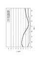
図4は、界面反射防止膜が形成されていない位相差素子のシミュレーションモデルを示す模式図である。この位相差素子は、透明基板を石英とし、斜方蒸着膜をTa2O5とした。また、表面のみに反射防止膜(AR)を設けた。[Phase difference element in which no interface antireflection film is formed]
FIG. 4 is a schematic diagram showing a simulation model of a retardation element in which no interface antireflection film is formed. In this retardation element, the transparent substrate was made of quartz, and the obliquely deposited film was made of Ta2 O5 . Further, an antireflection film (AR) was provided only on the surface.
また、図5は、石英基板及びTa2O5斜方蒸着膜の屈折率波長分散を示すグラフである。また、図6は、界面反射防止膜が形成されていない位相差素子の反射率を示すグラフである。FIG. 5 is a graph showing the refractive index wavelength dispersion of the quartz substrate and the Ta2 O5 oblique deposition film. FIG. 6 is a graph showing the reflectance of the retardation element in which the interface antireflection film is not formed.
図5及び図6から分かるように、石英基板と斜方蒸着膜には大きな屈折率差があり、図4に示す位相差素子の構造では、s偏光成分及びp偏光成分の双方の反射率(Rp,Rs)を下げるのは困難であることが分かった。 As can be seen from FIGS. 5 and 6, there is a large refractive index difference between the quartz substrate and the obliquely deposited film. In the structure of the phase difference element shown in FIG. 4, the reflectances of both the s-polarized component and the p-polarized component ( It has been found that it is difficult to reduce (Rp, Rs).
[界面反射防止膜が形成された位相差素子]
次に、透明基板と斜方蒸着膜との間に界面反射防止膜を形成した位相差素子についてシミュレーションを行った。位相差素子は、図7に示すように、透明基板と斜方蒸着膜との間に界面反射防止膜を形成した。それ以外は図4に示す位相差素子と同様に、透明基板11を石英とし、斜方蒸着膜13をTa2O5とした。また、表面のみに反射防止膜(AR)を設けた。[Phase difference element with interface antireflection film]
Next, a simulation was performed on a retardation element in which an interface antireflection film was formed between a transparent substrate and an oblique deposition film. As shown in FIG. 7, the phase difference element was formed with an interface antireflection film between the transparent substrate and the oblique deposition film. Other than that, like the retardation element shown in FIG. 4, the
図8は、Al2O3界面反射防止膜、石英基板及びTa2O5斜方蒸着膜の屈折率波長分散を示すグラフである。また、図9は、Al2O3界面反射防止膜が形成された位相差素子の反射率を示すグラフである。FIG. 8 is a graph showing the refractive index wavelength dispersion of the Al2 O3 interface antireflection film, the quartz substrate, and the Ta2 O5 oblique deposition film. FIG. 9 is a graph showing the reflectance of the retardation element on which the Al2 O3 interface antireflection film is formed.
図8及び図9から分かるように、Al2O3界面反射防止膜は、屈折率がTa2O5斜方蒸着膜よりも高く、青色波長帯域において反射率(Rp、Rs)の低減の効果が小さいことが分かった。As can be seen from FIGS. 8 and 9, the Al2 O3 interface antireflection film has a higher refractive index than the Ta2 O5 oblique deposition film, and the effect of reducing the reflectance (Rp, Rs) in the blue wavelength band. Was found to be small.
図10は、SiO2界面反射防止膜、石英基板及びTa2O5斜方蒸着膜の屈折率波長分散を示すグラフである。また、図11は、SiO2界面反射防止膜が形成された位相差素子の反射率を示すグラフである。FIG. 10 is a graph showing the refractive index wavelength dispersion of the SiO2 interface antireflection film, the quartz substrate, and the Ta2 O5 oblique deposition film. FIG. 11 is a graph showing the reflectance of the retardation element on which the SiO2 interface antireflection film is formed.
図10及び図11から分かるように、SiO2界面反射防止膜は、屈折率が石英基板よりも低く、青色波長帯域において反射率(Rp、Rs)の低減の効果が小さいことが分かった。As can be seen from FIGS. 10 and 11, the SiO2 interface antireflection film has a refractive index lower than that of the quartz substrate, and it has been found that the effect of reducing the reflectance (Rp, Rs) is small in the blue wavelength band.
次に、位相差素子の反射率が低くなる最適界面反射防止膜について、屈折率をシミュレーションにより求めた。 Next, the refractive index of the optimum interface antireflection film that reduces the reflectivity of the retardation element was determined by simulation.
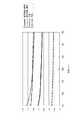
図12は、最適界面反射防止膜、石英基板及びTa2O5斜方蒸着膜の屈折率波長分散を示すグラフである。また、図13は、最適界面反射防止膜が形成された位相差素子の反射率を示すグラフである。FIG. 12 is a graph showing the refractive index wavelength dispersion of the optimum interface antireflection film, the quartz substrate, and the Ta2 O5 oblique deposition film. FIG. 13 is a graph showing the reflectance of the retardation element on which the optimum interface antireflection film is formed.
図12及び図13から分かるように、最適界面反射防止膜の屈折率は、石英基板よりも高く、Ta2O5斜方蒸着膜よりも低い。この最適界面反射防止膜は、反射率(Rp、Rs)の低減の効果が大きく、青色波長帯域において0.2%以下の反射率(Rp、Rs)が得られることが分かった。As can be seen from FIGS. 12 and 13, the refractive index of the optimum interface antireflection film is higher than that of the quartz substrate and lower than that of the Ta2 O5 oblique deposition film. It has been found that this optimum interface antireflection film has a great effect of reducing the reflectance (Rp, Rs), and a reflectance (Rp, Rs) of 0.2% or less can be obtained in the blue wavelength band.
以上より、界面反射防止膜の屈折率が、透明基板の屈折率よりも高く、斜方蒸着膜の屈折率よりも小さいことにより、位相差素子の反射率を低減させることが可能であることが分かった。 From the above, it is possible to reduce the reflectance of the retardation element by making the refractive index of the interface antireflection film higher than the refractive index of the transparent substrate and smaller than the refractive index of the oblique deposition film. I understood.
[3層構造による界面反射防止膜]
前述の最適界面反射防止膜は、単層で最適屈折率を満たす材料が存在しないため、積層による最適界面反射防止膜のシミュレーションを行った。その結果、最適設計膜厚が66nmの単層の最適界面反射防止膜は、SiO2膜とNb2O5膜とSiO2膜とがこの順に積層された3層構造膜で実現可能であることが分かった。[Three-layer structure interface antireflection film]
Since the above-mentioned optimum interface antireflection film does not have a material satisfying the optimum refractive index with a single layer, the optimum interface antireflection film by lamination was simulated. As a result, a single-layer optimum interface antireflection film having an optimum design film thickness of 66 nm can be realized by a three-layer structure film in which an SiO2 film, an Nb2 O5 film, and an SiO2 film are laminated in this order. I understood.
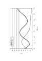
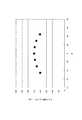
図14は、最適界面反射防止膜の反射率を示すグラフである。また、図15は、3層構造膜及び最適界面反射防止膜の反射率を示すグラフである。図15に示すグラフより、SiO2膜を76nm、Nb2O5膜を3.3nm、及びSiO2膜を44nm、この順番に積層することにより、反射率が最適界面反射防止膜の最適反射率とほぼ一致することが分かった。FIG. 14 is a graph showing the reflectance of the optimum interface antireflection film. FIG. 15 is a graph showing the reflectivity of the three-layer structure film and the optimum interface antireflection film. From the graph shown in FIG. 15, the SiO2 film is 76 nm, the Nb2 O5 film is 3.3 nm, and the SiO2 film is 44 nm. It was found that it almost matches.
また、図16は、3層構造膜のNb2O5膜の厚さを2.3nm、3.3nm、又は4.3nmとしたときの反射率を示すグラフである。図16に示すグラフより、Nb2O5膜の厚さが±1nm変化すると大幅に反射率が変化し、Nb2O5膜の厚さが重要であることが分かった。FIG. 16 is a graph showing the reflectance when the thickness of the Nb2 O5 film of the three-layer structure film is 2.3 nm, 3.3 nm, or 4.3 nm. From the graph shown in FIG. 16, Nb2 O5 when the thickness of the film changes ± 1 nm greatly reflectance is changed, the thickness of the Nb2 O5 film was found to be important.
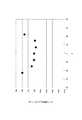
図17は、3層構造の第2層をAl2O3膜としたときの位相差素子の反射率を示すグラフである。3層構造のNb2O5膜をAl2O3膜に代えて最適化を試みたが、例えば、図17に示すように、Al2O5膜の屈折率が小さいため、青色波長帯域において反射率(Rp、Rs)の低減の効果が小さいことが分かった。FIG. 17 is a graph showing the reflectance of the retardation element when the second layer having the three-layer structure is an Al2 O3 film. Although optimization was attempted by replacing the Nb2 O5 film having a three-layer structure with an Al2 O3 film, for example, as shown in FIG. 17, since the refractive index of the Al2 O5 film is small, in the blue wavelength band, It was found that the effect of reducing reflectivity (Rp, Rs) was small.
図18は、3層構造の第2層をNb2O5膜としたときの位相差素子の反射率を示すグラフである。SiO2膜を95nm、Nb2O5膜を3.0nm、及びSiO2膜を35nmに最適化したところ、青色波長帯域において0.2%以下の反射率(Rp、Rs)が得られた。FIG. 18 is a graph showing the reflectance of the retardation element when the second layer having the three-layer structure is an Nb2 O5 film. When the SiO2 film was optimized to 95 nm, the Nb2 O5 film was optimized to 3.0 nm, and the SiO2 film was optimized to 35 nm, a reflectance (Rp, Rs) of 0.2% or less was obtained in the blue wavelength band.
また、図17及び図18に示す結果より、3層構造の第2層をTiO2、LaTiO3,Ta2O5などの高屈折材料で代用可能であることが分かった。Further, from the results shown in FIGS. 17 and 18, it was found that the second layer having the three-layer structure can be substituted with a high refractive material such as TiO2 , LaTiO3 , Ta2 O5 .
図19は、3層構造の界面反射防止膜を形成した位相差素子及び界面反射防止膜が形成されていない位相差素子の反射率を示すグラフである。図19に示すグラフから明らかのように、透明基板と斜方蒸着膜との間に、高屈折率膜と低屈折率膜とが交互に積層された界面反射防止膜を設けることにより、位相差素子の反射率(Rp、Rs)を低減させることができることが分かった。 FIG. 19 is a graph showing the reflectivity of a retardation element having a three-layer interface antireflection film and a retardation element having no interface antireflection film. As apparent from the graph shown in FIG. 19, by providing an interface antireflection film in which a high refractive index film and a low refractive index film are alternately laminated between a transparent substrate and an oblique deposition film, a phase difference is obtained. It was found that the reflectance (Rp, Rs) of the element can be reduced.
[斜方蒸着膜と界面反射防止膜との関係]
次に、SiO2膜、Nb2O5膜、及びSiO2膜をこの順番に積層した3層構造の界面反射防止膜と、斜方蒸着膜の屈折率との関係についてシミュレーションを行った。なお、波長450nmにおける透明基板の屈折率を1.47とした。[Relationship between oblique deposition film and interface antireflection film]
Next, simulation was performed on the relationship between the refractive index of the oblique deposition film and the three-layer interface antireflection film in which the SiO2 film, the Nb2 O5 film, and the SiO2 film were laminated in this order. The refractive index of the transparent substrate at a wavelength of 450 nm was 1.47.
図20は、斜方蒸着膜の屈折率に対する3層構造の界面反射防止膜を形成した位相差素子の反射率を示すグラフである。ここで、界面反射防止膜は、SiO2膜を93nm、Nb2O5膜を3nm、及びSiO2膜を35nm、この順番に積層した3層構造とした。FIG. 20 is a graph showing the reflectance of the retardation element in which the three-layer structure antireflection film is formed with respect to the refractive index of the oblique deposition film. Here, the interface antireflection film has a three-layer structure in which the SiO2 film is 93 nm, the Nb2 O5 film is 3 nm, and the SiO2 film is 35 nm in this order.
図20に示すグラフより、斜方蒸着膜の面内直交2軸x,yの屈折率noblx,nobly(noblx>nobly)のそれぞれが1.55以上1.7以下の範囲にあるとき、青色波長帯域(440〜510nm)の反射率が0.3%以下となることが分かった。From the graph shown in FIG. 20, the refractive indexes noblx and nobly (noblx > nobly ) of the in-plane orthogonal two axes x and y of the oblique deposition film are in the range of 1.55 or more and 1.7 or less. It was found that the reflectance in the blue wavelength band (440 to 510 nm) was 0.3% or less.
表1に、斜方蒸着膜の屈折率noblx,nobly(noblx>nobly)に対するNb2O5膜の有効膜厚範囲のシミュレーション結果を示す。Table 1 shows the simulation results of the effective film thickness range of the Nb2 O5 film with respect to the refractive indexes noblx , nobly (noblx > nobly ) of the oblique deposition film.
斜方蒸着膜の屈折率noblx,nobly(noblx>nobly)が1.55のときNb2O5膜の有効膜厚範囲は0.5〜3.5nmとなり、斜方蒸着膜の屈折率noblx,nobly(noblx>nobly)が1.70のときNb2O5膜の有効膜厚範囲は3.0〜5.5nmとなることが分かった。When the refractive index noblx , nobly (noblx > nobly ) of the oblique deposition film is 1.55, the effective film thickness range of the Nb2 O5 film is 0.5 to 3.5 nm. It was found that the effective film thickness range of the Nb2 O5 film is 3.0 to 5.5 nm when the refractive indexesnob1x andnobly (nob1x >nobly ) are 1.70.
次に、図21に示すように、3層構造の第2層のNb2O5膜を3nmに固定し、第1層のSiO2膜や第3層のSiO2膜の厚さを変えてシミュレーションを行った。図21に示すグラフより、第1層のSiO2膜及び第3層のSiO2膜の厚さが±10nm変動しても、反射率は大きく変動しないことが分かった。Next, as shown in FIG. 21, the Nb2 O5 film of the second layer having the three-layer structure is fixed to 3 nm, and the thicknesses of the SiO2 film of the first layer and the SiO2 film of the third layer are changed. A simulation was performed. From the graph shown in FIG. 21, it was found that the reflectivity did not vary greatly even when the thicknesses of the first layer SiO2 film and the third layer SiO2 film varied by ± 10 nm.
これらのシミュレーション結果より、低屈折率膜、高屈折率膜、及び低屈折率膜をこの順番に積層した3層構造の界面反射防止膜は、低屈折率膜の屈折率nLが1.5より小さく、高屈折率膜の屈折率nHが2.0より大きいことにより、反射率の低減が可能であることが分かった。そして、斜方蒸着膜の面内直交2軸x,yの屈折率noblx,nobly(noblx>nobly)のそれぞれが1.55以上1.7以下の範囲にあり、3層構造の高屈折率膜の膜厚が0.1以上5.5nm以下の範囲にあることにより、青色波長帯域(440〜510nm)において0.3%以下の反射率を実現可能であることが分かった。From these simulation results, the interface antireflection film having the three-layer structure in which the low refractive index film, the high refractive index film, and the low refractive index film are laminated in this order has a refractive index nL of the low refractive index film of 1.5. It has been found that the reflectance can be reduced when the refractive index nH of the high refractive index film is smaller than 2.0.Each of the refractive indexes noblx and nobly (noblx > nobly ) of the in-plane orthogonal two axes x and y of the oblique vapor deposition film is in the range of 1.55 to 1.7 and has a three-layer structure. It has been found that when the film thickness of the high refractive index film is in the range of 0.1 to 5.5 nm, a reflectance of 0.3% or less can be realized in the blue wavelength band (440 to 510 nm).
<4.2 1/4波長板の作製>
次に、前述のシミュレーション結果を実証するために、1/4波長板を作製した。図22は、実施例の位相差素子の構造を示す模式図である。また、図23は、比較例の位相差素子の構造を示す模式図である。<4.2 Production of 1/4 wavelength plate>
Next, in order to verify the above-mentioned simulation result, a quarter wavelength plate was produced. FIG. 22 is a schematic diagram illustrating the structure of the retardation element of the example. FIG. 23 is a schematic diagram showing the structure of a retardation element of a comparative example.
[実施例]
石英基板上に、石英基板の屈折率と、斜方蒸着膜の屈折率の中間の値を持つ誘電体膜(界面反射防止膜)をスパッタにより成膜した。この界面反射防止膜は、相対的に高屈折率物質と低屈折率物質の2種類の物質を交互に積層した構造とした。具体的には、石英基板/SiO2(93m)/Nb2O5(3nm)/SiO2(35nm)の構造とし、界面反射防止膜の最上部は、斜方蒸着膜の光学特性が変動しないように、基板と同材質のSiO2とした。[Example]
On the quartz substrate, a dielectric film (interface antireflection film) having an intermediate value between the refractive index of the quartz substrate and the refractive index of the obliquely deposited film was formed by sputtering. The interface antireflection film has a structure in which two types of materials, a relatively high refractive index material and a low refractive index material, are alternately stacked. Specifically, the structure is quartz substrate / SiO2 (93 m) / Nb2 O5 (3 nm) / SiO2 (35 nm), and the optical properties of the oblique deposition film do not vary at the top of the interface antireflection film. Thus, the same material as the substrate was SiO2 .
次に、Ta2O5を主成分とした蒸着材料を石英基板の法線方向に対して蒸着源が70°になるように蒸着を行った。この際、7nm成膜するごとに石英基板を面内方向に180°回転させることにより、成膜方向が異なる多数層からなる斜方蒸着膜を作製した。斜方蒸着膜の全層の膜厚は、青色波長帯域で1/4波長板として機能する約900nmとした。Next, we deposited deposition material mainly composed of Ta2 O5 as the vapor deposition source with respect to the normal direction of the quartz substrate is 70 °. At this time, each time the film was formed to 7 nm, the quartz substrate was rotated 180 ° in the in-plane direction to produce an oblique vapor deposition film composed of multiple layers having different film forming directions. The thickness of all layers of the oblique vapor deposition film was about 900 nm which functions as a quarter wavelength plate in the blue wavelength band.
斜方蒸着後、色抜き、及び柱状組織間に吸着している水分を蒸発させるために200℃でのアニール処理を行った。アニール後、斜方蒸着膜への大気中の水分の出入りを防止するため、プラズマTEOS−CVDにより緻密性の高い誘電体(SiO2膜)を成膜した。そして、これらの構造体の表裏両面にスパッタにより積層誘電体による反射防止膜を成膜した。以上のようにして図22に示す実施例の位相差素子を作製した。After oblique deposition, annealing was performed at 200 ° C. to remove the color and evaporate the moisture adsorbed between the columnar structures. After annealing, a high-density dielectric (SiO2 film) was formed by plasma TEOS-CVD in order to prevent moisture in the atmosphere from entering and exiting the obliquely deposited film. Then, an antireflection film made of a laminated dielectric was formed on both the front and back surfaces of these structures by sputtering. The phase difference element of the example shown in FIG. 22 was produced as described above.
[比較例]
界面反射防止膜を形成せずに、石英基板上に2層からなる斜方蒸着膜を作製した以外は、実施例と同様にして比較例の位相差素子を作製した。[Comparative example]
A retardation element of a comparative example was produced in the same manner as in the example, except that a two-layer oblique vapor deposition film was produced on a quartz substrate without forming an interface antireflection film.
石英基板上にTa2O5を主成分とした蒸着材料を、基板法線方向に対して蒸着源が70°になるように蒸着を行った。この際、750nm成膜したのち基板を180°回転させ、成膜方向が異なる2層からなる斜方蒸着膜を作製した。2層の膜厚は、青色波長帯域で1/4波長板として機能する約1500nmとした。以上のようにして図23に示す比較例の位相差素子を作製した。A vapor deposition material mainly composed of Ta2 O5 was deposited on a quartz substrate so that the vapor deposition source was 70 ° with respect to the normal direction of the substrate. At this time, after forming the film at 750 nm, the substrate was rotated 180 ° to prepare an oblique vapor deposition film composed of two layers having different film forming directions. The thickness of the two layers was about 1500 nm, which functions as a quarter wavelength plate in the blue wavelength band. As described above, the retardation element of the comparative example shown in FIG. 23 was produced.
[実施例及び比較例の光学特性]
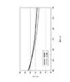
図24は、リタデーション(Re)の波長依存性を示すグラフである。実施例及び比較例の位相差素子は、460nmのリタデーションが約115nmであり、1/4波長板として機能することが確認できた。[Optical Properties of Examples and Comparative Examples]
FIG. 24 is a graph showing the wavelength dependence of retardation (Re). It was confirmed that the retardation elements of Examples and Comparative Examples had a retardation of 460 nm of about 115 nm and functioned as a quarter wavelength plate.
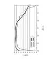
図25は、透過率の波長依存性を示すグラフである。また、図26は、反射率の波長依存性を示すグラフである。実施例の位相差素子は、比較例の位相差素子よりも透過率が1%程度高く、反射率が0.5%程度低い値を示すことが分かった。反射率の低下は、界面反射防止膜、及び斜方蒸着膜の多層化の効果であり、反射率を低下させたことで、透過率も向上させることができた。 FIG. 25 is a graph showing the wavelength dependence of transmittance. FIG. 26 is a graph showing the wavelength dependence of reflectance. It was found that the retardation element of the example had a transmittance about 1% higher and a reflectance about 0.5% lower than the retardation element of the comparative example. The decrease in reflectance is an effect of multilayering of the interface antireflection film and the oblique deposition film, and the transmittance can also be improved by reducing the reflectance.
次に、界面反射防止膜の効果を見積もるため、シミュレーションを行った。実施例で作製した位相差素子について、SiO2(93m)/Nb2O5(3nm)/SiO2(35nm)の3層構造の界面反射防止膜の有無について、青色波長帯域の反射率を計算した。Next, a simulation was performed to estimate the effect of the interface antireflection film. For the retardation element produced in the example, the reflectance in the blue wavelength band is calculated for the presence or absence of an interface antireflection film having a three-layer structure of SiO2 (93 m) / Nb2 O5 (3 nm) / SiO2 (35 nm). did.
図27は、実施例及び比較例の位相差素子の反射率を示すグラフである。界面反射防止膜がない比較例の位相差素子に比べ、界面反射防止膜がある実施例の位相差素子は、反射率の平均値及びピーク値の両者とも半減する効果が示された。 FIG. 27 is a graph showing the reflectivity of the retardation elements of the example and the comparative example. Compared to the retardation element of the comparative example without the interface antireflection film, the retardation element of the example with the interface antireflection film showed an effect of halving both the average value and the peak value of the reflectance.
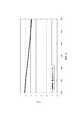
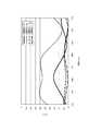
また、本技術においては、反射率の低減に加えて、視野角依存性改善の効果もあることが分かった。図28及び図29は、実施例の位相差素子のリタデーションの入射角度依存性を示すグラフである。また、図30は、比較例の位相差素子のリタデーションの入射角度依存性を示すグラフである。 In addition to the reduction in reflectance, the present technology has been found to have an effect of improving the viewing angle dependency. FIG. 28 and FIG. 29 are graphs showing the incident angle dependence of the retardation of the retardation element of the example. FIG. 30 is a graph showing the incident angle dependency of retardation of the retardation element of the comparative example.
図31に示すように、位相差素子面内において、進相軸(斜方蒸着方向と平行な方向)をx軸、遅相軸(斜方蒸着方向と垂直な方向)をy軸、及び素子法線方向をz軸としたとき、z軸方向からの入射光角度を0とした。また、xz平面上に入射光を傾けた場合の角度をθとし、yz平面上に傾けた場合の角度をφとした。なお、図28〜30に示すグラフは、入射光角度0のときのリタデーションの値で規格化したものである。 As shown in FIG. 31, in the phase difference element plane, the fast axis (direction parallel to the oblique deposition direction) is the x axis, the slow axis (direction perpendicular to the oblique deposition direction) is the y axis, and the element. The incident light angle from the z-axis direction was set to 0 when the normal direction was the z-axis. In addition, an angle when the incident light is tilted on the xz plane is θ, and an angle when the incident light is tilted on the yz plane is φ. The graphs shown in FIGS. 28 to 30 are normalized by the retardation value when the incident light angle is zero.
実施例の位相差素子は、光軸に対してリタデーションの分布が左右対称となっていることが分かった。比較例の位相差素子は、θ方向のリタデーションは比較的左右対称となっているが、φ方向のリタデーションは、正確な測定を行うことができなかった。その理由は、比較例のように斜方蒸着膜が光の波長より十分に小さくない膜厚で積層されている場合、複屈折の軸が異なる2つの位相差素子が重なったようにみなされ、単純な「屈折率差と軸方向」という評価を行うことはできないからである。そのため、比較例の位相差素子は、角度依存性をもつ入射光に対して使用することは困難である。 It was found that the retardation element of the example has a symmetrical distribution of retardation with respect to the optical axis. In the retardation element of the comparative example, the retardation in the θ direction is relatively bilaterally symmetric, but the retardation in the φ direction could not be accurately measured. The reason is that when the oblique vapor deposition film is laminated with a film thickness that is not sufficiently smaller than the wavelength of light as in the comparative example, it is considered that two phase difference elements having different birefringence axes are overlapped, This is because a simple evaluation of “refractive index difference and axial direction” cannot be performed. Therefore, it is difficult to use the phase difference element of the comparative example with respect to incident light having angle dependency.
実施例の位相差素子は、光の波長より十分に小さな膜厚で積層しているため、各層の複屈折の軸が無視できるようになり、全層で一つの軸(実施例の場合、z軸方向)をもつ位相差素子と見なすことができるため、角度依存性を有する入射光に対して、適切な位相差素子となり得ることが分かった。 Since the phase difference element of the example is laminated with a film thickness sufficiently smaller than the wavelength of light, the birefringence axis of each layer can be ignored, and one axis in all layers (in the case of the example, z Since it can be regarded as a phase difference element having an axial direction), it has been found that it can be an appropriate phase difference element for incident light having angle dependency.
以上のように、界面反射防止膜を導入し、さらに斜方蒸着膜の1層あたりの膜厚を使用波長以下とすることにより、反射率が低減され、かつ角度依存性が左右対称に改善されることがわかった。 As described above, by introducing an interface antireflection film and further reducing the film thickness per layer of the obliquely deposited film to the working wavelength or less, the reflectance is reduced and the angle dependency is improved symmetrically. I found out.
これらの実施例及び比較例の位相差素子を青色波長帯域用の1/4波長板として、反射型液晶プロジェクターに適用したところ、実施例の位相差素子を適用した場合、比較例の位相差素子を適用した場合と比べて明るさで1%、コントラストで5%の向上が見られた。当然、本技術を緑色波長帯域用、赤色用の1/4波長板として適用することで、明るさ及びコントラストのさらなる向上が期待できる。 When the phase difference elements of these examples and comparative examples are applied to a reflective liquid crystal projector as a quarter wavelength plate for a blue wavelength band, the phase difference elements of the comparative examples are applied when the phase difference elements of the examples are applied. Compared to the case of applying, improvement of 1% in brightness and 5% in contrast was observed. Naturally, further improvement in brightness and contrast can be expected by applying the present technology as a quarter wavelength plate for green wavelength band and red.
なお、本発明はこれらの実施例に限定されるものではなく、本発明の趣旨を逸脱しない範囲で種々の変形や変更が行えることは勿論である。例えば、前述した実施例の位相差素子は、各層の膜厚が等しいため、複屈折の軸はz軸方向となるが、例えば、各層の膜厚を変えることで、軸方向を任意に傾けるようにしてもよい。 In addition, this invention is not limited to these Examples, Of course, a various deformation | transformation and change can be performed in the range which does not deviate from the meaning of this invention. For example, in the retardation element of the above-described embodiment, since the thickness of each layer is equal, the birefringence axis is in the z-axis direction. For example, the axial direction can be arbitrarily tilted by changing the thickness of each layer. It may be.
また、前述した実施例では、青色波長帯域の1/4波長板について説明したが、本技術は、緑色波長帯域、赤色波長帯域の1/4波長板や各チャンネルの1/2波長板、広帯域の1/4波長板、1/2波長板、位相差補償素子などに応用してもよい。 In the above-described embodiments, the quarter wavelength plate of the blue wavelength band has been described. However, the present technology can be applied to the quarter wavelength plate of the green wavelength band, the red wavelength band, the half wavelength plate of each channel, and the broadband. The present invention may be applied to a quarter wavelength plate, a half wavelength plate, a phase difference compensation element, and the like.
11 透明基板、 12 界面反射防止膜、 13 斜方蒸着膜、 14 CVD誘電体膜、 15A,15B 反射防止膜、 21 偏光ビームスプリッタ、 22 1/4波長板、 23 液晶セル DESCRIPTION OF
図1は、本発明の一実施の形態に係る位相差素子を示す概略断面図である。図1に示すように、位相差素子1は、透明基板11と、透明基板11上に高屈折率膜と低屈折率膜とが交互に積層された界面反射防止膜12と、界面反射防止膜12上に誘電体材料が180°異なる2方向から各層の厚さが使用波長以下であるように交互に斜方蒸着された斜方蒸着膜13と、斜方蒸着膜13上に形成されたCVD(Chemical Vapor Deposition)誘電体膜14とを備える。また、これらの表裏両面に積層誘電体からなる反射防止膜15A、15Bを備える。FIG. 1 is a schematic cross-sectional view showing a phase difference element according to an embodiment of the present invention. As shown in FIG. 1, a
ステップS2では、界面反射防止膜12に、斜方蒸着により高屈折率材料を成膜する。具体的には、成膜する度に透明基板11を面内方向に180°回転させることにより、成膜方向が異なる多数層からなる斜方蒸着膜13を成膜する。この際、1層あたりの膜厚を波長以下とする多層構造とする。また、斜方蒸着膜中に耐湿性向上の目的で低屈折率物質を充填してもよい。高屈折率材料としては、Ta、Zr、Ti、Si、Al、Nb、Laなどの酸化物、又はそれらを組み合わせたものを用いることができる。In step S2, ahigh refractive index material is formed on the
図17は、3層構造の第2層をAl2O3膜としたときの位相差素子の反射率を示すグラフである。3層構造のNb2O5膜をAl2O3膜に代えて最適化を試みたが、例えば、図17に示すように、Al2O3膜の屈折率が比較的小さいため、青色波長帯域において反射率(Rp、Rs)の低減の効果が小さいことが分かった。FIG. 17 is a graph showing the reflectance of the retardation element when the second layer having the three-layer structure is an Al2 O3 film. An optimization was attempted by replacing the Nb2 O5 film having a three-layer structure with an Al2 O3 film. For example, as shown in FIG. 17, the refractive index of theAl2O3 film isrelatively small, so that the blue wavelength It was found that the effect of reducing the reflectance (Rp, Rs) was small in the band.
図19は、3層構造の界面反射防止膜を形成した位相差素子及び界面反射防止膜が形成されていない位相差素子の反射率を示すグラフである。図19に示すグラフから明らかなように、透明基板と斜方蒸着膜との間に、高屈折率膜と低屈折率膜とが交互に積層された界面反射防止膜を設けることにより、位相差素子の反射率(Rp、Rs)を低減させることができることが分かった。FIG. 19 is a graph showing the reflectivity of a retardation element having a three-layer interface antireflection film and a retardation element having no interface antireflection film. Asapparent from the graph shown in FIG. 19, between the transparent substrate and the oblique deposition film, by providing the interface anti-reflection film and the high refractive index film and a low refractive index film are alternately laminated, the phase difference It was found that the reflectance (Rp, Rs) of the element can be reduced.
Claims (13)
Translated fromJapanese誘電体材料が180°異なる2方向から交互に斜方蒸着され、各層の厚さが使用波長以下である斜方蒸着膜と、
前記透明基板と前記斜方蒸着膜との間に高屈折率膜と低屈折率膜とが交互に積層され、屈折率が前記透明基板の屈折率よりも高く、前記斜方蒸着膜の屈折率よりも小さい界面反射防止膜と
を備える位相差素子。A transparent substrate;
Diagonal vapor deposition films in which dielectric materials are alternately obliquely deposited from two directions different from each other by 180 °, and the thickness of each layer is equal to or less than a use wavelength;
A high refractive index film and a low refractive index film are alternately laminated between the transparent substrate and the oblique deposition film, and the refractive index is higher than the refractive index of the transparent substrate, and the refractive index of the oblique deposition film. A retardation element comprising a smaller interface antireflection film.
前記界面反射防止膜上に誘電体材料を180°異なる2方向から交互に斜方蒸着して各層の厚さが使用波長以下である斜方蒸着膜を形成する
位相差素子の製造方法。A high refractive index film and a low refractive index film are alternately laminated on a transparent substrate to form an interface antireflection film whose refractive index is higher than that of the transparent substrate and smaller than that of the oblique deposition film. And
A method for manufacturing a retardation element, wherein a dielectric material is alternately obliquely evaporated from two directions different from each other by 180 ° on the interface antireflection film to form an obliquely evaporated film having a thickness of each layer equal to or less than a use wavelength.
Priority Applications (2)
| Application Number | Priority Date | Filing Date | Title |
|---|---|---|---|
| JP2011109688AJP2012242449A (en) | 2011-05-16 | 2011-05-16 | Phase difference element and manufacturing method for the same |
| US13/473,100US8842365B2 (en) | 2011-05-16 | 2012-05-16 | Phase difference element and method for manufacturing the same |
Applications Claiming Priority (1)
| Application Number | Priority Date | Filing Date | Title |
|---|---|---|---|
| JP2011109688AJP2012242449A (en) | 2011-05-16 | 2011-05-16 | Phase difference element and manufacturing method for the same |
Related Child Applications (1)
| Application Number | Title | Priority Date | Filing Date |
|---|---|---|---|
| JP2015159361ADivisionJP6027199B2 (en) | 2015-08-12 | 2015-08-12 | Phase difference element and manufacturing method thereof |
Publications (1)
| Publication Number | Publication Date |
|---|---|
| JP2012242449Atrue JP2012242449A (en) | 2012-12-10 |
Family
ID=47174683
Family Applications (1)
| Application Number | Title | Priority Date | Filing Date |
|---|---|---|---|
| JP2011109688APendingJP2012242449A (en) | 2011-05-16 | 2011-05-16 | Phase difference element and manufacturing method for the same |
Country Status (2)
| Country | Link |
|---|---|
| US (1) | US8842365B2 (en) |
| JP (1) | JP2012242449A (en) |
Cited By (14)
| Publication number | Priority date | Publication date | Assignee | Title |
|---|---|---|---|---|
| WO2014168185A1 (en)* | 2013-04-10 | 2014-10-16 | デクセリアルズ株式会社 | Phase contrast compensation element and projection-type image projection device |
| JP2015068935A (en)* | 2013-09-27 | 2015-04-13 | デクセリアルズ株式会社 | Retardation element and method for manufacturing the same, liquid crystal display device and method for manufacturing the same, and projection type image display device |
| JP2015082035A (en)* | 2013-10-23 | 2015-04-27 | デクセリアルズ株式会社 | Retardation element and method for manufacturing the same, liquid crystal display device, and projection type image display device |
| JP2015082010A (en)* | 2013-10-22 | 2015-04-27 | デクセリアルズ株式会社 | Inorganic optical element |
| JP2015092282A (en)* | 2015-01-20 | 2015-05-14 | デクセリアルズ株式会社 | Manufacturing method for wavelength plate |
| JP2018124591A (en)* | 2013-07-11 | 2018-08-09 | デクセリアルズ株式会社 | Method for manufacturing bundle structure |
| WO2019102902A1 (en)* | 2017-11-21 | 2019-05-31 | デクセリアルズ株式会社 | Optical element and projection-type image display apparatus |
| JP2019095776A (en)* | 2018-09-21 | 2019-06-20 | デクセリアルズ株式会社 | Optical element and projection type image display device |
| JP2019133171A (en)* | 2019-03-04 | 2019-08-08 | デクセリアルズ株式会社 | Method for manufacturing retardation compensation element |
| JP2020042083A (en)* | 2018-09-07 | 2020-03-19 | デクセリアルズ株式会社 | Optical element, liquid crystal display device, and projection image display device |
| JP2021086013A (en)* | 2019-11-28 | 2021-06-03 | デクセリアルズ株式会社 | Optical element, manufacturing method therefor, and projection image display device |
| JP2021117445A (en)* | 2020-01-29 | 2021-08-10 | デクセリアルズ株式会社 | Method for manufacturing polarizing plate, optical instrument and polarizing plate |
| US11269218B2 (en) | 2018-01-31 | 2022-03-08 | Dexerials Corporation | Phase difference compensation element, liquid crystal display device and projection type image display device |
| JP7655476B2 (en) | 2019-11-28 | 2025-04-02 | デクセリアルズ株式会社 | Phase difference compensation element, liquid crystal display device, and projection type image display device |
Families Citing this family (15)
| Publication number | Priority date | Publication date | Assignee | Title |
|---|---|---|---|---|
| EP2985641B1 (en)* | 2013-04-10 | 2022-03-23 | Dexerials Corporation | Phase difference compensating element and projection-type image projecting device |
| US9366784B2 (en) | 2013-05-07 | 2016-06-14 | Corning Incorporated | Low-color scratch-resistant articles with a multilayer optical film |
| US9359261B2 (en) | 2013-05-07 | 2016-06-07 | Corning Incorporated | Low-color scratch-resistant articles with a multilayer optical film |
| US9110230B2 (en) | 2013-05-07 | 2015-08-18 | Corning Incorporated | Scratch-resistant articles with retained optical properties |
| US9684097B2 (en) | 2013-05-07 | 2017-06-20 | Corning Incorporated | Scratch-resistant articles with retained optical properties |
| US9703011B2 (en) | 2013-05-07 | 2017-07-11 | Corning Incorporated | Scratch-resistant articles with a gradient layer |
| US9335444B2 (en) | 2014-05-12 | 2016-05-10 | Corning Incorporated | Durable and scratch-resistant anti-reflective articles |
| US11267973B2 (en) | 2014-05-12 | 2022-03-08 | Corning Incorporated | Durable anti-reflective articles |
| CN105268110B (en)* | 2014-06-19 | 2018-03-13 | 昆山科技大学 | Jaundice phototherapy device |
| US9790593B2 (en) | 2014-08-01 | 2017-10-17 | Corning Incorporated | Scratch-resistant materials and articles including the same |
| JP2018536177A (en) | 2015-09-14 | 2018-12-06 | コーニング インコーポレイテッド | High light transmittance and scratch resistant anti-reflective article |
| JP6289526B2 (en)* | 2016-03-03 | 2018-03-07 | キヤノン株式会社 | Optical element and optical system having the same |
| CN114085037B (en) | 2018-08-17 | 2023-11-10 | 康宁股份有限公司 | Inorganic oxide article with thin durable anti-reflective structure |
| CN112859226A (en)* | 2019-11-28 | 2021-05-28 | 迪睿合株式会社 | Phase difference compensation element, liquid crystal display device, and projection type image display device |
| US12147009B2 (en) | 2020-07-09 | 2024-11-19 | Corning Incorporated | Textured region to reduce specular reflectance including a low refractive index substrate with higher elevated surfaces and lower elevated surfaces and a high refractive index material disposed on the lower elevated surfaces |
Citations (3)
| Publication number | Priority date | Publication date | Assignee | Title |
|---|---|---|---|---|
| JP2000047133A (en)* | 1997-08-18 | 2000-02-18 | Ricoh Co Ltd | Scanning imaging lens and optical scanning device |
| JP2005292646A (en)* | 2004-04-02 | 2005-10-20 | Nitto Denko Corp | Method for producing antireflection film and antireflection film |
| JP2006171328A (en)* | 2004-12-15 | 2006-06-29 | Fuji Photo Film Co Ltd | Phase difference compensation element, optical modulation system, liquid crystal display device, and liquid crystal projector |
Family Cites Families (2)
| Publication number | Priority date | Publication date | Assignee | Title |
|---|---|---|---|---|
| JP5773576B2 (en)* | 2010-04-01 | 2015-09-02 | キヤノン株式会社 | Anti-reflection structure and optical equipment |
| JP5854628B2 (en)* | 2011-04-26 | 2016-02-09 | キヤノン株式会社 | Optical system and optical apparatus using the same |
- 2011
- 2011-05-16JPJP2011109688Apatent/JP2012242449A/enactivePending
- 2012
- 2012-05-16USUS13/473,100patent/US8842365B2/enactiveActive
Patent Citations (3)
| Publication number | Priority date | Publication date | Assignee | Title |
|---|---|---|---|---|
| JP2000047133A (en)* | 1997-08-18 | 2000-02-18 | Ricoh Co Ltd | Scanning imaging lens and optical scanning device |
| JP2005292646A (en)* | 2004-04-02 | 2005-10-20 | Nitto Denko Corp | Method for producing antireflection film and antireflection film |
| JP2006171328A (en)* | 2004-12-15 | 2006-06-29 | Fuji Photo Film Co Ltd | Phase difference compensation element, optical modulation system, liquid crystal display device, and liquid crystal projector |
Cited By (30)
| Publication number | Priority date | Publication date | Assignee | Title |
|---|---|---|---|---|
| WO2014168185A1 (en)* | 2013-04-10 | 2014-10-16 | デクセリアルズ株式会社 | Phase contrast compensation element and projection-type image projection device |
| JP2014219672A (en)* | 2013-04-10 | 2014-11-20 | デクセリアルズ株式会社 | Phase difference compensation element and projection type image projection device |
| US9784898B2 (en) | 2013-04-10 | 2017-10-10 | Dexerials Corporation | Phase difference compensating element and projection-type image projecting device |
| US10732335B2 (en) | 2013-07-11 | 2020-08-04 | Dexerials Coporation | Polarizing plate having absorption layer comprising only tantalum and niobium |
| US11262491B2 (en) | 2013-07-11 | 2022-03-01 | Dexerials Corporation | Polarizing plate having alternately stacked layers having different deposition directions |
| JP2018124591A (en)* | 2013-07-11 | 2018-08-09 | デクセリアルズ株式会社 | Method for manufacturing bundle structure |
| JP2018124590A (en)* | 2013-07-11 | 2018-08-09 | デクセリアルズ株式会社 | Manufacturing method of bundle structure |
| JP2015068935A (en)* | 2013-09-27 | 2015-04-13 | デクセリアルズ株式会社 | Retardation element and method for manufacturing the same, liquid crystal display device and method for manufacturing the same, and projection type image display device |
| JP2015082010A (en)* | 2013-10-22 | 2015-04-27 | デクセリアルズ株式会社 | Inorganic optical element |
| WO2015060213A1 (en)* | 2013-10-22 | 2015-04-30 | デクセリアルズ株式会社 | Inorganic optical element and method for manufacturing same |
| US9964670B2 (en) | 2013-10-22 | 2018-05-08 | Dexerials Corporation | Inorganic optical element having a birefringent film with a columnar structure and a protective film formed thereon and method for manufacturing same |
| JP2015082035A (en)* | 2013-10-23 | 2015-04-27 | デクセリアルズ株式会社 | Retardation element and method for manufacturing the same, liquid crystal display device, and projection type image display device |
| JP2015092282A (en)* | 2015-01-20 | 2015-05-14 | デクセリアルズ株式会社 | Manufacturing method for wavelength plate |
| US11294114B2 (en) | 2017-11-21 | 2022-04-05 | Dexerials Corporation | Optical element and projection image display apparatus |
| WO2019102902A1 (en)* | 2017-11-21 | 2019-05-31 | デクセリアルズ株式会社 | Optical element and projection-type image display apparatus |
| JP2019095554A (en)* | 2017-11-21 | 2019-06-20 | デクセリアルズ株式会社 | Optical element and projection type image display device |
| US11573362B2 (en) | 2017-11-21 | 2023-02-07 | Dexerials Corporation | Optical element and projection image display apparatus |
| US11269218B2 (en) | 2018-01-31 | 2022-03-08 | Dexerials Corporation | Phase difference compensation element, liquid crystal display device and projection type image display device |
| JP2020042083A (en)* | 2018-09-07 | 2020-03-19 | デクセリアルズ株式会社 | Optical element, liquid crystal display device, and projection image display device |
| JP7236230B2 (en) | 2018-09-07 | 2023-03-09 | デクセリアルズ株式会社 | Optical element, liquid crystal display device and projection type image display device |
| US11537008B2 (en) | 2018-09-07 | 2022-12-27 | Dexerials Corporation | Optical element, liquid crystal display device, and projection-type image display device |
| JP7092630B2 (en) | 2018-09-21 | 2022-06-28 | デクセリアルズ株式会社 | Optical element and projection type image display device |
| JP2019095776A (en)* | 2018-09-21 | 2019-06-20 | デクセリアルズ株式会社 | Optical element and projection type image display device |
| JP2019133171A (en)* | 2019-03-04 | 2019-08-08 | デクセリアルズ株式会社 | Method for manufacturing retardation compensation element |
| JP7141353B2 (en) | 2019-03-04 | 2022-09-22 | デクセリアルズ株式会社 | Manufacturing method of phase difference compensating element |
| JP2021086013A (en)* | 2019-11-28 | 2021-06-03 | デクセリアルズ株式会社 | Optical element, manufacturing method therefor, and projection image display device |
| JP7655476B2 (en) | 2019-11-28 | 2025-04-02 | デクセリアルズ株式会社 | Phase difference compensation element, liquid crystal display device, and projection type image display device |
| JP2021117445A (en)* | 2020-01-29 | 2021-08-10 | デクセリアルズ株式会社 | Method for manufacturing polarizing plate, optical instrument and polarizing plate |
| JP7320461B2 (en) | 2020-01-29 | 2023-08-03 | デクセリアルズ株式会社 | Polarizing plate, optical device, and method for producing polarizing plate |
| US11867938B2 (en) | 2020-01-29 | 2024-01-09 | Dexerials Corporation | Polarizing plate having outermost layer of anti-reflection layer recessed towards substrate |
Also Published As
| Publication number | Publication date |
|---|---|
| US20120293732A1 (en) | 2012-11-22 |
| US8842365B2 (en) | 2014-09-23 |
Similar Documents
| Publication | Publication Date | Title |
|---|---|---|
| JP2012242449A (en) | Phase difference element and manufacturing method for the same | |
| JP6502021B2 (en) | Phase difference compensation element and projection type image projector | |
| CN101173994B (en) | Film design for positive and/or negative C-plates | |
| JP5984771B2 (en) | Phase difference element and method for manufacturing the same, liquid crystal display device and method for manufacturing the same, and projection-type image display device | |
| CA2569970A1 (en) | Thin-film optical retarders | |
| US9279928B2 (en) | Retardation element comprising a birefringent multilayer structure, liquid crystal display device, and projection display device | |
| CN101218524A (en) | Phase difference compensation element, liquid crystal device, and projection display apparatus | |
| US9952368B2 (en) | Polarization conversion element and optical device | |
| CN110095833B (en) | Phase difference compensation element, liquid crystal display device, and projection type image display device | |
| US11294114B2 (en) | Optical element and projection image display apparatus | |
| CN105988158B (en) | Wavelength plate and optical device | |
| CN106033158B (en) | Phase difference element, liquid crystal display device, and projection type image display device | |
| JP6027199B2 (en) | Phase difference element and manufacturing method thereof | |
| JP2007310052A (en) | Wave plate | |
| JP7236225B2 (en) | Phase difference compensation element, liquid crystal display device and projection type image display device | |
| JP7141353B2 (en) | Manufacturing method of phase difference compensating element | |
| JP2019095776A (en) | Optical element and projection type image display device | |
| CN110716257A (en) | Method for manufacturing phase difference element, and projection type image display device | |
| Ma et al. | Non-polarizing broadband dichroic mirror | |
| CN112859227B (en) | Phase difference compensation element, liquid crystal display device, and projection type image display device | |
| JP2017049594A (en) | Phase difference element and manufacturing method of the same, liquid crystal display, and projection type image display unit | |
| CN115997145A (en) | Phase difference film, liquid crystal projector and contrast adjustment method | |
| Liu et al. | Design of large acceptance angle polarizing beam splitter for laser-based displays |
Legal Events
| Date | Code | Title | Description |
|---|---|---|---|
| A621 | Written request for application examination | Free format text:JAPANESE INTERMEDIATE CODE: A621 Effective date:20140414 | |
| A977 | Report on retrieval | Free format text:JAPANESE INTERMEDIATE CODE: A971007 Effective date:20150121 | |
| A131 | Notification of reasons for refusal | Free format text:JAPANESE INTERMEDIATE CODE: A131 Effective date:20150217 | |
| A521 | Written amendment | Free format text:JAPANESE INTERMEDIATE CODE: A523 Effective date:20150417 | |
| A02 | Decision of refusal | Free format text:JAPANESE INTERMEDIATE CODE: A02 Effective date:20150512 |