JP2012238882A - Method and apparatus for slope to threshold conversion for process state monitoring and endpoint detection - Google Patents
Method and apparatus for slope to threshold conversion for process state monitoring and endpoint detectionDownload PDFInfo
- Publication number
- JP2012238882A JP2012238882AJP2012164925AJP2012164925AJP2012238882AJP 2012238882 AJP2012238882 AJP 2012238882AJP 2012164925 AJP2012164925 AJP 2012164925AJP 2012164925 AJP2012164925 AJP 2012164925AJP 2012238882 AJP2012238882 AJP 2012238882A
- Authority
- JP
- Japan
- Prior art keywords
- value
- transition point
- monitored
- transition
- threshold
- Prior art date
- Legal status (The legal status is an assumption and is not a legal conclusion. Google has not performed a legal analysis and makes no representation as to the accuracy of the status listed.)
- Pending
Links
- 238000000034methodMethods0.000titleclaimsabstractdescription152
- 230000008569processEffects0.000titleclaimsabstractdescription97
- 238000001514detection methodMethods0.000titleclaimsabstractdescription79
- 238000012544monitoring processMethods0.000titleclaimsdescription15
- 238000006243chemical reactionMethods0.000title1
- 230000007704transitionEffects0.000claimsabstractdescription227
- 238000012545processingMethods0.000claimsdescription107
- 239000004065semiconductorSubstances0.000claimsdescription79
- 230000008859changeEffects0.000claimsdescription39
- 235000012431wafersNutrition0.000claimsdescription31
- 238000005259measurementMethods0.000claimsdescription20
- 238000004891communicationMethods0.000claimsdescription11
- 239000000126substanceSubstances0.000claimsdescription9
- 238000005530etchingMethods0.000claimsdescription8
- 238000012986modificationMethods0.000claimsdescription7
- 230000004048modificationEffects0.000claimsdescription7
- 230000008021depositionEffects0.000claimsdescription3
- 238000001228spectrumMethods0.000claimsdescription3
- 230000004044responseEffects0.000claims1
- 239000000758substrateSubstances0.000description20
- 238000004519manufacturing processMethods0.000description16
- 238000010586diagramMethods0.000description12
- 238000009826distributionMethods0.000description11
- 238000005498polishingMethods0.000description10
- 230000003287optical effectEffects0.000description8
- 238000012546transferMethods0.000description7
- 238000013459approachMethods0.000description6
- 229910008326Si-YInorganic materials0.000description4
- 229910006773Si—YInorganic materials0.000description4
- 239000007788liquidSubstances0.000description4
- 239000000203mixtureSubstances0.000description4
- 230000035699permeabilityEffects0.000description4
- 238000003860storageMethods0.000description4
- 230000007774longtermEffects0.000description3
- 239000012528membraneSubstances0.000description3
- 230000006399behaviorEffects0.000description2
- 230000015572biosynthetic processEffects0.000description2
- 238000010924continuous productionMethods0.000description2
- 238000013500data storageMethods0.000description2
- 238000013213extrapolationMethods0.000description2
- 238000011065in-situ storageMethods0.000description2
- 238000000059patterningMethods0.000description2
- 238000011112process operationMethods0.000description2
- 239000007787solidSubstances0.000description2
- 229910001220stainless steelInorganic materials0.000description2
- 239000010935stainless steelSubstances0.000description2
- 239000000463materialSubstances0.000description1
Images


Classifications
- G—PHYSICS
- G05—CONTROLLING; REGULATING
- G05B—CONTROL OR REGULATING SYSTEMS IN GENERAL; FUNCTIONAL ELEMENTS OF SUCH SYSTEMS; MONITORING OR TESTING ARRANGEMENTS FOR SUCH SYSTEMS OR ELEMENTS
- G05B23/00—Testing or monitoring of control systems or parts thereof
- G05B23/02—Electric testing or monitoring
- G05B23/0205—Electric testing or monitoring by means of a monitoring system capable of detecting and responding to faults
- G05B23/0218—Electric testing or monitoring by means of a monitoring system capable of detecting and responding to faults characterised by the fault detection method dealing with either existing or incipient faults
- G05B23/0243—Electric testing or monitoring by means of a monitoring system capable of detecting and responding to faults characterised by the fault detection method dealing with either existing or incipient faults model based detection method, e.g. first-principles knowledge model
- G05B23/0254—Electric testing or monitoring by means of a monitoring system capable of detecting and responding to faults characterised by the fault detection method dealing with either existing or incipient faults model based detection method, e.g. first-principles knowledge model based on a quantitative model, e.g. mathematical relationships between inputs and outputs; functions: observer, Kalman filter, residual calculation, Neural Networks
- H—ELECTRICITY
- H01—ELECTRIC ELEMENTS
- H01L—SEMICONDUCTOR DEVICES NOT COVERED BY CLASS H10
- H01L21/00—Processes or apparatus adapted for the manufacture or treatment of semiconductor or solid state devices or of parts thereof
- H01L21/02—Manufacture or treatment of semiconductor devices or of parts thereof
- H—ELECTRICITY
- H01—ELECTRIC ELEMENTS
- H01L—SEMICONDUCTOR DEVICES NOT COVERED BY CLASS H10
- H01L22/00—Testing or measuring during manufacture or treatment; Reliability measurements, i.e. testing of parts without further processing to modify the parts as such; Structural arrangements therefor
- H—ELECTRICITY
- H01—ELECTRIC ELEMENTS
- H01L—SEMICONDUCTOR DEVICES NOT COVERED BY CLASS H10
- H01L22/00—Testing or measuring during manufacture or treatment; Reliability measurements, i.e. testing of parts without further processing to modify the parts as such; Structural arrangements therefor
- H01L22/20—Sequence of activities consisting of a plurality of measurements, corrections, marking or sorting steps
- H01L22/26—Acting in response to an ongoing measurement without interruption of processing, e.g. endpoint detection, in-situ thickness measurement
Landscapes
- Engineering & Computer Science (AREA)
- Physics & Mathematics (AREA)
- Manufacturing & Machinery (AREA)
- Computer Hardware Design (AREA)
- Microelectronics & Electronic Packaging (AREA)
- Power Engineering (AREA)
- General Physics & Mathematics (AREA)
- Evolutionary Computation (AREA)
- Mathematical Physics (AREA)
- Artificial Intelligence (AREA)
- Automation & Control Theory (AREA)
- Condensed Matter Physics & Semiconductors (AREA)
- Testing Or Measuring Of Semiconductors Or The Like (AREA)
- Drying Of Semiconductors (AREA)
- Mechanical Treatment Of Semiconductor (AREA)
Abstract
Description
Translated fromJapanese本発明は概して、半導体製造に関し、特に半導体製造作業における処理とウェーハ状態モニタリングとのリアルタイム計測に関する。 The present invention relates generally to semiconductor manufacturing, and more particularly to real-time measurement of processing and wafer condition monitoring in semiconductor manufacturing operations.
(発明の背景)
半導体製造の間、下にある基板が形成、修正および様々な層の除去、ブランケットまたはパターン化の対象になるところには複数のステップが存在する。小さい特徴寸法、厳しい表面の平面性要求、スループットを上げることを絶え間なく探求することと相まって、処理された膜のターゲットにされた性質(厚さ、抵抗、平面性、透過性、化学成分等)が達成されたとき、すなわち、現在の工程ステップに対する終了点が得られたとき、工程パラメータを停止または変更することが強く所望される。もちろん、現在の工程ステップの後にその後の製造ステップに遷移する半導体製造ステップの中には、明確なウェーハ特徴を得るタスクを成し遂げているものがある。(Background of the Invention)
During semiconductor manufacturing, there are multiple steps where the underlying substrate is subject to formation, modification and removal of various layers, blankets or patterning. Targeted properties of the processed membrane (thickness, resistance, planarity, permeability, chemical composition, etc.) coupled with small feature dimensions, demanding surface flatness requirements, and continually seeking to increase throughput When is achieved, i.e., when an end point has been obtained for the current process step, it is highly desirable to stop or change the process parameters. Of course, some semiconductor manufacturing steps that transition to subsequent manufacturing steps after the current process step have accomplished the task of obtaining distinct wafer characteristics.
ウェーハ特徴を制御するリアルタイム計測は現在必要不可欠な存在であり、その結果、特定の処理作業の終了点または遷移点が決定され得る。半導体作業と関連するパラメータのin−situモニターは、処理作業の終了点または遷移点に関する有用な情報を提供する。通常、工程でウェーハに強くリンクされる物体(ウェーハ自体または他の物質)の性質は、遷移に先立って、かつ遷移の後に単調量変化を経験し、遷移自体の間に急激な性質の変異を経験する。これは、モニターされるシステムが十分に小さいときと、遷移が検査空間の観察点と同時に生じるときとの場合に、信号変動をモニターするステップ状の性質をもたらす。より大きなシステム(例えば、半導体ウェーハ)については、工程パラメータ変化に対応するデータ点に関連付けられたステップ状の遷移点を傾斜変化に移す時間分類があり、これにより終了点または遷移点の指標を生成する。しかしながら、傾斜変化検出は微分係数(derivative)の使用を必要とし、この微分係数はこのアプローチを複雑にする減少した信号対雑音比と関連する。 Real-time metrology that controls wafer characteristics is now indispensable so that the end point or transition point of a particular processing operation can be determined. An in-situ monitor of parameters associated with the semiconductor operation provides useful information regarding the end or transition point of the processing operation. Typically, the nature of an object (wafer itself or other material) that is strongly linked to the wafer in the process will experience a monotonic change prior to and after the transition, and abrupt changes in properties during the transition itself. experience. This results in a step-like nature of monitoring signal variations when the monitored system is small enough and when transitions occur simultaneously with the observation point in the examination space. For larger systems (eg, semiconductor wafers), there is a time classification that shifts stepped transition points associated with data points corresponding to process parameter changes to slope changes, thereby generating an endpoint or transition point indicator. To do. However, slope change detection requires the use of a derivative, which is associated with a reduced signal-to-noise ratio that complicates the approach.
図1は、処理作業(例えば、平坦化処理作業)の間長期にわたってモニターされる半導体ウェーハの厚さに関するグラフである。線100は処理作業中の終了点/遷移点を決定する赤外線(IR)ベースのセンサに関連する値を表す。線102は、処理中の長期にわたる半導体ウェーハの厚さを記録する複数の渦電流センサ(ECS)に関連する値を表す。図に示すように、領域104は終了点/遷移点が生じる時間を表す。領域104では、一般傾斜は線102および線100遷移と一体になった。しかしながら、IRモニターまたは渦電流モニターのどちらか一方でモニターされている信号は、運転毎に変化する顕著なかつ可変性のバックグラウンドノイズと重畳される。従って、微分係数ベースの傾斜を計測することによって終了点を決定するとき、信号対雑音レベルは終了点決定の安定性と確実性とに影響する。よって、傾斜ベースの分析に予測される遷移点のインライン決定は、半導体作業に必要な確固たるデータを提供しない。 FIG. 1 is a graph of semiconductor wafer thickness that is monitored over time during a processing operation (eg, a planarization processing operation).
そのため、従来技術の問題を解決し、遷移点がモニターされた工程パラメータの傾斜ベースの遷移から生じる場合の工程で安定かつ確実な遷移点決定を提供する方法と装置とを提供する必要がある。 Therefore, there is a need to provide a method and apparatus that solves the problems of the prior art and provides a stable and reliable transition point determination in the process when the transition point results from a slope-based transition of the monitored process parameter.
(発明の概要)
該して言えば、本発明は遷移点の決定の確実性と安定性とを向上させるために、微分係数ベースのデータを分析する必要性を排除し、かつ、閾値分析から遷移点の決定を可能にすることによってこれら必要性を満たす。本発明は、方法、システム、コンピュータ読取可能な媒体または装置として含む多数の方法で実行され得ることを理解されたい。本発明のいくつかの創意工夫に満ちた実施形態が以下に記載される。(Summary of Invention)
In other words, the present invention eliminates the need to analyze derivative-based data to improve the certainty and stability of transition point determination, and makes transition point determination from threshold analysis. It fulfills these needs by making it possible. It should be understood that the present invention can be implemented in numerous ways, including as a method, system, computer readable medium or device. Several inventive embodiments of the present invention are described below.
一実施形態では、傾斜ベース検出タスクを閾値ベース検出タスクに変換する方法が提供される。この方法は、モニターされている処理(process)の値に対応する一組の点の近似方程式を定義することから開始する。その後、モニターされている処理の現在の点における期待値が予測される。次に、モニターされている処理の現在の点における測定値と対応する期待値との間の差が計算される。それから、逐次点の差がモニターされることにより測定値と期待値との間の偏差値を検出する。次に、モニターされている処理の遷移点が偏差値の検出に基づいて識別される。 In one embodiment, a method for converting a slope-based detection task into a threshold-based detection task is provided. The method begins by defining a set of point approximation equations that correspond to the values of the process being monitored. Thereafter, the expected value at the current point of the process being monitored is predicted. Next, the difference between the measured value at the current point of the process being monitored and the corresponding expected value is calculated. Then, the difference between the measured value and the expected value is detected by monitoring the difference between successive points. Next, the transition point of the monitored process is identified based on the detection of the deviation value.
別の実施形態では、傾斜ベース変化の遷移点を閾値検出から検出する方法が提供される。この方法は、遷移点と関連するパラメータをモニターすることから開始する。それから、パラメータの予測値がモニターされた処理パラメータの過去の値から計算される。予測値はモニターされている処理パラメータの現在値に一致する。次に、閾値が決定される。その後、現在値と予測値との間の差はトラックされる。次に、差が閾値を越えるとき、遷移点が識別される。 In another embodiment, a method is provided for detecting a slope-based change transition point from threshold detection. The method begins by monitoring parameters associated with transition points. The predicted value of the parameter is then calculated from the past value of the monitored process parameter. The predicted value matches the current value of the process parameter being monitored. Next, a threshold is determined. Thereafter, the difference between the current value and the predicted value is tracked. A transition point is then identified when the difference exceeds a threshold.
さらに別の実施形態では、傾斜変化遷移の遷移点をリアルタイムで閾値決定から検出することが可能である半導体処理システムが提供される。このシステムは、処理されている半導体ウェーハと関連する明確なパラメータが得られるまで半導体ウェーハを処理するように構成された処理モジュールを含む。処理システムは、処理作業に関連する処理パラメータをモニターするように構成されたセンタを含む。このシステムは、センサと通信する検出器を含む。この検出器は、測定値が傾斜変化から遷移点を示す場合、測定値を予測値と比較するように構成される。予測値はそれ以前に測定した値から導かれる。この検出器はさらに、測定値と対応する予測値との差をトラックすることにより、遷移点における変化を強化(enhance)し、閾偏差値が決定されることを可能にするように構成される。閾偏差値は処理作業に関連する遷移点を示す。 In yet another embodiment, a semiconductor processing system is provided that can detect a transition point of a slope change transition from a threshold determination in real time. The system includes a processing module configured to process a semiconductor wafer until a defined parameter associated with the semiconductor wafer being processed is obtained. The processing system includes a center configured to monitor processing parameters associated with processing operations. The system includes a detector in communication with the sensor. The detector is configured to compare the measured value with a predicted value when the measured value indicates a transition point from a slope change. Predicted values are derived from previously measured values. The detector is further configured to enhance the change at the transition point and allow the threshold deviation value to be determined by tracking the difference between the measured value and the corresponding predicted value. . The threshold deviation value indicates a transition point related to the processing operation.
さらにまた別の実施形態では、傾斜ベース検出タスクを閾値ベース検出タスクに変換するプログラム命令を有するコンピュータ読取可能な媒体が提供される。コンピュータ読取可能な媒体は、モニターされている処理の値に対応する一組の点の近似方程式を規定するプログラム命令と、モニターされている処理の現在点における期待値を予測するプログラム命令とを含む。モニターされている処理の現在点における計測値と対応する期待値との差を計算するプログラム命令が提供される。差をモニターすることにより、計測値と期待値との間の偏差値を検出するプログラム命令と、偏差値の検出に基づいてモニターされている処理の遷移点を識別するプログラム命令とが含まれる。 In yet another embodiment, a computer readable medium having program instructions for converting a tilt based detection task into a threshold based detection task is provided. The computer-readable medium includes program instructions that define a set of approximate points corresponding to the value of the process being monitored, and program instructions that predict the expected value at the current point of the process being monitored. . Program instructions are provided for calculating the difference between the measured value at the current point of the monitored process and the corresponding expected value. A program instruction for detecting a deviation value between the measured value and the expected value by monitoring the difference and a program instruction for identifying a transition point of the process being monitored based on the detection of the deviation value are included.
本発明の他の局面と利点とは、例として本発明の原理を説明する添付の図面と併せて以下の詳細な説明から明らかになる。
本発明は、添付の図面と併せて以下の詳細な説明によって容易に理解され、同様の参照番号は同様の構造要素を示す。Other aspects and advantages of the present invention will become apparent from the following detailed description, taken in conjunction with the accompanying drawings, illustrating by way of example the principles of the invention.
The present invention will be readily understood by the following detailed description in conjunction with the accompanying drawings, and like reference numerals designate like structural elements.
本発明は、半導体処理作業中、遷移点の確実かつ安定した測定を提供するシステム、装置および方法を示す。しかしながら、本発明はこれら特定の詳細のいくつかまたは全てをなしで実行され得ることは当業者にとって明らかである。別の場合では、よく知られた処理作業は本発明を不必要に分かりにくくしないために詳細に記載されていない。図1は(発明の背景)部分に記載される。 The present invention shows a system, apparatus and method that provides reliable and stable measurement of transition points during semiconductor processing operations. However, it will be apparent to those skilled in the art that the present invention may be practiced without some or all of these specific details. In other instances, well known process operations have not been described in detail in order not to unnecessarily obscure the present invention. FIG. 1 is described in the (Background of the invention) part.
本発明の実施形態は、傾斜検出タスクを閾値検出タスクに変換するシステムおよび方法、ならびに移転の標示である移転特徴を増幅するシステムおよび方法を提供する。閾値動作(threshold behavior)は、ゼロまたは定信号のバックグラウンドでステップ状の特徴を生成し、かつ、より単純なアルゴリズム、より高い信号対雑音比およびより確実な検出可能性を提供する。遷移点/終了点の閾値ベース決定は、傾斜ベース決定に比べてさらに高い安全性と確実性とを提供する。同様に、より安定したかつ確実なトリガリング条件が半導体作業に対して提供される。つまり、遷移点/終了点は高度な信頼度を持って決定されるので、実質的に正確な測定を要求する下流作業(downstream operation)がインライン計測から開始され得る。その結果、関連作業の半導体スループットが付随して増加され得る。微分係数分析に関する処理トレーシング信号の傾斜における小さい変化から生じる混乱は、トレーシング信号を閾値タイプに変換することによって除去される。ここで用いられる終了点および遷移点という用語は互換性があるということを理解されたい。ターゲット変化が生じている、ターゲット状態が達成される場合、またはモニターされるパラメータと関連するある値の到達が終了点または他の処理作業の開始といったイベントを開始させることに用いられる場合、終了点および遷移点という用語は半導体処理または他の処理における任意の点に関連し得ることは当業者にとって明白である。 Embodiments of the present invention provide a system and method for converting a tilt detection task to a threshold detection task, and a system and method for amplifying a transfer feature that is an indication of transfer. Threshold behavior generates a stepped feature with zero or constant signal background and provides a simpler algorithm, higher signal-to-noise ratio and more reliable detectability. Transition point / end point threshold-based determination provides even greater safety and certainty than slope-based determination. Similarly, more stable and reliable triggering conditions are provided for semiconductor operations. That is, since the transition point / end point is determined with a high degree of reliability, a downstream operation requiring substantially accurate measurement can be started from in-line measurement. As a result, the semiconductor throughput of related work can be increased concomitantly. Confusion resulting from small changes in the slope of the processed tracing signal for derivative analysis is eliminated by converting the tracing signal to a threshold type. It should be understood that the terms end point and transition point as used herein are interchangeable. An end point if a target change has occurred, a target state has been achieved, or the arrival of some value associated with a monitored parameter is used to initiate an event such as an end point or the start of another processing task It will be apparent to those skilled in the art that the terms and transition points may relate to any point in semiconductor processing or other processing.
図2は、赤外線(IR)ベースのトレースに関するグラフであり、ここで遷移領域におけるノイズレベルは本発明の一実施形態に従って遷移点を示すようにスムーズ化される。ここで、領域106においてノイズレベルはトレース108をスムーズ化された線のように示すように実質的に除去される。図に示すように、傾斜は領域106におけるスムーズ化されたトレース108遷移と一体になった。しかしながら、モニターされている作業と関連するノイズ(例えば、化学機械的平坦化(CMP)作業またはエッチング作業)は、リアルタイムの安定したかつ再現性のある読取りが終了点または他の作業の開始といったイベントを開始させることを妨げる。図2は温度に関連する赤外線信号を説明するが、他の信号、例えば渦電流センサ、振動、光学屈折等は同様の性質を示すことを理解されたい。つまり、スムーズ化された傾斜は遷移点を示す。しかしながら、前述したように、バックグラウンドノイズは、安定したかつ正確なリアルタイム読取りが傾斜読取りすることを防ぐ。以下により詳細に説明されるように、傾斜測定を閾値測定に変換することにより、傾斜測定と関連する微分係数測定について分析されている小さい差に影響を与えるノイズレベルに関連する不確実性を除去する。よって、リアルタイムにおいて遷移点をはるか正確に検出することが可能になる。遷移点を示す傾斜における小さい変化は、傾斜測定のノイズによって遮蔽される。しかしながら、ここで記載される実施形態は、実質的にノイズを除去することにより遷移点の決定に影響を与えない。 FIG. 2 is a graph for an infrared (IR) based trace, where the noise level in the transition region is smoothed to indicate a transition point according to one embodiment of the present invention. Here, in
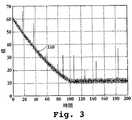
図3は、長期にわたる信号トレースに関する例示的なグラフであり、ここで、時間の期間は遷移点を含む。ここで、信号110は長期にわたってプロットされる。一実施形態では、信号110は処理パラメータを検出するように構成された渦電流センサからもたらされ、半導体作業中の遷移点を示す。半導体作業中の遷移点を検出する他の信号(例えば、赤外線、振動、光学ベースの信号等)はここに含まれ得ることを理解されたい。図に示すように、信号110は信号に関連する相当量のノイズを有しているが、長期にわたる傾向が時間100における遷移点を示す。当業者は、傾斜ベースの決定ではバックグラウンドノイズが原因でここでは不安定な結果を生み出すことを理解する。 FIG. 3 is an exemplary graph for signal traces over time, where the time period includes transition points. Here, signal 110 is plotted over time. In one embodiment, signal 110 is derived from an eddy current sensor configured to detect a processing parameter and indicates a transition point during semiconductor operation. It should be understood that other signals that detect transition points during semiconductor operation (eg, infrared, vibration, optical based signals, etc.) may be included here. As shown, signal 110 has a significant amount of noise associated with the signal, but a long-term trend indicates a transition point at
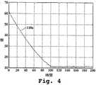
図4は、スムーズ化されてノイズを除去した図3の信号に関する例示的なグラフである。ここで、線110aは、信号をスムーズ化するために通常の正弦ノイズフィルターが適用された。信号110aが長期にわたる渦電流センサの値を表すところで、遷移点はほぼ時間100における傾斜の変化によって示される。前述したように、スムーズ化された傾斜はリアルタイムで安定したかつ正確な方法で生成されることができない。従って、傾斜ベースの決定はここでは実行可能な代案ではない。 FIG. 4 is an exemplary graph for the signal of FIG. 3 that has been smoothed to remove noise. Here, a normal sine noise filter is applied to the
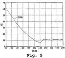
図5は、本発明の一実施形態に従って図3の実際の信号の点から生成された予測された信号に関する例示的なグラフである。ここでは、選択した区間のデータフロー点の近似方程式を用いて、本発明の一実施形態の最近のデータ読取りを予測する。図8Aと図8Bとを参照しながらより詳細に説明されるように、予測信号は、本発明の一実施形態に従って近似方程式を実信号の履歴データ点に適用して、予測されたリアルタイムデータ点を生成することによって生成される。図5に示されるように、線110bによって表される予測信号は、遷移点を表す時間100において、図3および図4の実信号から逸脱し始める。近似方程式は任意の多項方程式であり得ることを理解されたい。例えば、近似方程式は一次方程式、放物線型方程式または他のより高い累乗の方程式の形式をとり得る。 FIG. 5 is an exemplary graph for a predicted signal generated from the actual signal points of FIG. 3 in accordance with one embodiment of the present invention. Here, an approximate equation of the data flow point of the selected interval is used to predict the recent data reading of an embodiment of the present invention. As will be described in more detail with reference to FIGS. 8A and 8B, the predicted signal can be estimated by applying an approximation equation to the historical data points of the real signal in accordance with one embodiment of the present invention. Is generated by generating As shown in FIG. 5, the predicted signal represented by
図6は、本発明の一実施形態に従って、様々な時間点における実信号と対応する予測信号との差を計算することによって生成された偏差信号に関する例示的なグラフである。ここで、線112は長期にわたる予測信号と実信号との差を表す。領域114はノイズ区域(corridor of noise)を現す。つまり、実信号と予測信号との差にオフセットが当てはめられることによりノイズ区域を規定することができ、ここで、ノイズ区域の外側にある点は遷移点に妥当な点であると考えられる。本質的に、ノイズ区域は実際値と予測値との差の周りの境界を規定する。一実施形態において、オフセットは3掛ける標準偏差値(すなわち、3б)に選ばれる。よって、ノイズ分布がガウス分布のように構成される場合、3бは分布における全ての点のうち99.7%をカバーする。したがって、1000点のうち、ノイズ区域の外側に実際あり、遷移点の開始点ではない一点に対する確率は3×10⁻³である。モニターされている処理の性質次第で、この確率は減少または増加して許容されるレベルの正確さを提供し得る。FIG. 6 is an exemplary graph for a deviation signal generated by calculating a difference between a real signal and a corresponding predicted signal at various time points in accordance with an embodiment of the present invention. Here,
図7は、本発明の一実施形態に従って、互いに重畳された図4、図5および図6のグラフを含む例示的なグラフであり、遷移点の閾値決定を明らかにする。ここでは、図4からの線110a、図5からの線110bおよび線112が互いに重畳されている。さらに、ノイズ区域114も示されている。偏差信号、すなわち、実信号と予測信号との差を表す線112は、時間100の遷移点においてノイズ区域を超え始めることが理解されたい。以下により詳細に説明されるように、(ノイズの)3б区域は遷移点が検出されているというより高いまたはより低い信頼水準を与えるために調整され得る。例えば、高度な正確度および精密度を要求する処理は、より低い程度の正確度および精密度を要求する処理よりも広いノイズ区域を使用し得る。他の実施形態では、ノイズ区域の境界の外側に1つ以上の連続点が遷移点を認めることを開始するのに要求され得る。 FIG. 7 is an exemplary graph including the graphs of FIGS. 4, 5 and 6 superimposed on each other, in accordance with one embodiment of the present invention, demonstrating transition point threshold determination. Here, the
図8Aは、本発明の一実施形態に従う実信号と予測信号とのトレースを示す例示的なグラフである。線120は、長期にわたる処理パラメータ読取りのプロットを表す。処理パラメータは一実施形態において膜の厚さと一体になることを理解されたい。グラフの領域121は遷移前の領域を表し、他方でグラフの領域123は遷移後の領域を表す。よって、線120は2つの連続的な処理(例えば、遷移前領域の処理および遷移後領域の処理)を表しており、2つの処理の間には遷移点という形で割込みがある。遷移点はここで1つの状態から他の状態への変化を示す。ここで記載された実施形態は半導体処理を参照するが、この方法論は遷移が生じており、傾斜検出処理が1つの状態から他の状態への遷移を記録し得る場合の任意のシステムに適用され得ることを理解されたい。 FIG. 8A is an exemplary graph illustrating traces of real and predicted signals according to one embodiment of the present invention.
今なお図8Aを参照して、前区分またはデータ区間(例えば、領域121の区分n)は後の時間点における値を予測するのに用いられる。一実施形態では、多項方程式(例えば、放物線型方程式)を用いて、最近のデータ読取りに対応する予測値を導く。ここで、データの区分(データ区間とも呼ばれる)を取って、距離mから与えられるデータ値が計算される。当業者は、一実施形態において、データ値を出すのに用いられる放物線型(またはより高い累乗)の近似は、Y=a1tn+a2tn-1...+anの形式であることを理解する。ここで、Yは予測値(y座標の値)を表しており、tは時間(x座標の値)を表している。もちろんここでは、以前のデータはそのデータが関連するそれぞれの領域のダイナミクスを表していると仮定される。Still referring to FIG. 8A, the previous section or data interval (eg, section n of region 121) is used to predict a value at a later time point. In one embodiment, a polynomial equation (eg, a parabolic equation) is used to derive a predicted value corresponding to a recent data reading. Here, taking a data section (also called a data section), a data value given from the distance m is calculated. One skilled in the art will recognize that in one embodiment, the parabolic (or higher power) approximation used to generate the data values is Y = a1 tn + a2 tn−1 . . . + Understand that in the form of an. Here, Y represents a predicted value (y-coordinate value), and t represents time (x-coordinate value). Of course, here it is assumed that the previous data represents the dynamics of the respective region to which the data relates.
よって、検出装置(すなわち、センサ)によって測定される実信号は、近似方程式から計算される予測信号と比較され得る。実信号と予測信号とは、遷移が生じない限り、かつ、映写(補外)距離が大きすぎない限りは実質的に等しい。つまり、実信号の値と予測信号の値との差(Si−Yと表され、ここでSiは実信号でありYは予測信号である)はノイズレベル内で0に近接する。しかしながら、遷移が生じるとすぐに、実信号と予測値との差は0より徐々に大きくなり始め(Si−Y>0)、図8AのΔ122で表される。従って、この時点で閾値が実信号と予測値とが逸脱するところを検出するのに用いられ得る。さらに説明されるように、傾斜検出処理を閾値検出処理に変換することは、遷移に関連する変化を強化(増幅)し、その結果、遷移がより正確にかつ精密に識別され得る。 Thus, the actual signal measured by the detector (ie, sensor) can be compared with the predicted signal calculated from the approximate equation. The actual signal and the predicted signal are substantially equal unless a transition occurs and the projection (extrapolation) distance is not too large. That is, the difference between the actual signal value and the predicted signal value (expressed as Si-Y, where Si is the actual signal and Y is the predicted signal) is close to 0 within the noise level. However, as soon as the transition occurs, the difference between the actual signal and the predicted value begins to gradually increase from 0 (Si−Y> 0) and is represented by Δ122 in FIG. 8A. Therefore, at this point, the threshold can be used to detect where the actual signal deviates from the predicted value. As will be further described, converting the slope detection process to a threshold detection process enhances (amplifies) changes associated with the transition so that the transition can be more accurately and precisely identified.
図8Bは、本発明の一実施形態に従って、最初の信号値に関するグラフと、実信号と予測信号との間の偏差に関する対応するグラフとである。図8Bの上のグラフは、図8Aの実信号を表す。例えば、半導体処理モニタリングに関して、線120は赤外線センサ、渦電流センサ、振動センサ、温度センサ、反射スペクトルを検出するように構成されたセンサ等からの信号と関連するトレースを表し得る。時間ttにおいて生じる遷移は偏差トレース128(デルタトレースとも呼ばれる)から検出される。領域124と領域126とは、予測値が実信号からそれぞれ正の差と負の差として実信号から逸脱する領域を表す。FIG. 8B is a graph for the initial signal value and a corresponding graph for the deviation between the real signal and the predicted signal, in accordance with one embodiment of the present invention. The upper graph of FIG. 8B represents the real signal of FIG. 8A. For example, for semiconductor processing monitoring,
図8Bのデルタトレース128は、長期にわたる実信号と予測信号との差を表す。領域114はノイズ区域を表す。デルタトレース128および実信号のトレース120は各トレースに関連するバックグラウンドノイズを有する可能性があることを理解されたい。従って、トレース120は図3のトレースに類似する可能性があり、デルタトレース128は図6のトレースに類似する可能性がある。つまり、トレースはスムーズな線であるよりもむしろ、各トレースに関連するノイズを有する可能性がある。従って、ノイズ区域はノイズレベルを考慮に入れるように構成され、その結果、ノイズレベルは遷移点の決定に影響を与えない。同時に、大きさ(ノイズ区域のオフセットに関連して)が選ばれ、その結果、遷移がノイズレベルを超えて生じ、つまり、ノイズ区域が遷移点を遮蔽するほど大きくない。 The
一実施形態では、ノイズ区域のオフセットはデルタトレース128の3倍標準偏差(3б)に設定される。よって、ノイズがガウス分布である場合、3бは分布の全ての点のうち99.7%をカバーする。前述したように、ノイズ区域の外側にあり、遷移点の開始点ではない一点に対して3×10⁻³の確率があり、各1000個の点のうち3つの点が実際に規定された3б区間の外側にあり得ることを意味している。図9を参照しながらさらに説明されるように、ノイズ区域の外側にある多数の連続点は、遷移点の開始を示すことにより偽った判断(false positive)の可能性をさらに減らすために要求され得る。一実施形態では、オフセットは、ノイズ区域の外側の合理的に多数の連続点が用いられる場合、または3бより大きいノイズ区域が用いられる場合、必ずしも必要ではない。ノイズ区域の外側にあるいずれの数の連続点も、遷移点のトリガーとして定義され得ることを理解されたい。遷移点に達したことを示すのに必要とされる連続点の数が高ければ高いほど、実遷移点が得られたという信頼度がより強い。よって、精密な作業について偽った判断は費用がかかり、回復不能な損傷を引き起こす場合、ノイズ区域の外側の3つ以上の連続点が高度な信頼度を提供するのに選ばれ得る。作業がそれほど厳しくない場合、3つの点より少ない点を選ぶことが所望され得る。In one embodiment, the noise zone offset is set to 3 times the standard deviation (3б) of the
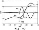
図8Cは、図8Aおよび図8Bの実トレースとデルタトレースとを示すグラフであり、予測値トレースが重畳されており、これら全ては傾斜ベースタスクを閾値ベースタスクに本発明の一実施形態に従って変換する際に使用される。トレース120は実センサ読取りを表す。トレース136は放物線状に補外した予測値を表す。トレース128は、実センサ読取りと対応する予測値との差であるデルタトレースを表す。放物線状に補外した予測値は、データ点の選択した区間と関連する放物線型近似と、最近のデータ読取りに対する放物線型予測とを含む。デルタトレース128は、現在点と多数の以前の連続点について放物線状に補外した予測値を減算することによって計算される。よって、閾値は、デルタトレースがしっかりとノイズレベルを超えているとき規定され得る。例えば、遷移点が生じたことを認める前に多数のノイズレベルの外にある連続点を規定することは、遷移点決定が正確であるという高い信頼度レベルを提供する。当業者は、遷移点がここで用いられる終了点を含むことを理解する。放物線型方程式がこの実施形態において近似方程式として用いられているが、任意の多項方程式が近似方程式として用いられ得、それは実センサ読取りによって規定される曲線の形が近似方程式の型に影響を与えるからであることを理解されたい。 FIG. 8C is a graph showing the actual and delta traces of FIGS. 8A and 8B with superimposed predictor traces, all of which convert slope-based tasks to threshold-based tasks according to one embodiment of the present invention. Used when doing.
図3および図6を参照して、図6のデルタトレースアプローチの閾値決定が図3の傾斜ベースのアプローチよりも優れていることが分かる。つまり、傾斜ベースの決定におけるノイズは傾斜における小さい変化を隠すが、閾値ベースの決定におけるノイズは、遷移点の認知を開始する前にオフセットを規定することによって、またはノイズ区域の外側にある多数の連続点を要求することによって、関心事として排除される。遷移点が達成されるとすぐに、他の所定の作業が開始し得、または現在の作業の終了点が生じ得ることを理解されたい。半導体製造(例えば、エッチング、堆積、CMP作業または他の表面改質処理)に関して、第1の層は追加、除去、平坦化または改質され得、その後半導体ウェーハはこの処理ツールまたは異なる処理ツールで別のモジュールに遷移され得る。 3 and 6, it can be seen that the threshold determination of the delta trace approach of FIG. 6 is superior to the slope-based approach of FIG. That is, noise in slope-based decisions hides small changes in slope, but noise in threshold-based decisions can be made by defining offsets before starting to recognize transition points, or multiple By requesting a continuity point, it is eliminated as a concern. It should be understood that as soon as the transition point is achieved, other predetermined tasks may begin or end points of the current task may occur. For semiconductor manufacturing (eg, etching, deposition, CMP operations or other surface modification processes), the first layer can be added, removed, planarized, or modified, after which the semiconductor wafer is processed with this processing tool or a different processing tool. It can be transitioned to another module.
図9は、本発明の一実施形態に従って、傾斜ベース検出タスクを閾値ベース検出タスクに変換する方法についての方法作業に関するフローチャートである。この方法は作業140で開始し、ここで近似方程式が一組の点について規定される。一組の点に対する近似方程式は、モニターされている処理の値に対応する。例えば、多項方程式(例えば、放物線型方程式)は前述したように近似方程式であり得る。モニターされている処理は、渦電流センサ、赤外線センサ、温度センサ、振動センサ等からモニターされ得る。この方法はそれから作業142に進み、ここでモニターされている処理の現在点における期待値が予測される。ここで、多項方程式が多数の連続点のデータ区分を取り、現在点の期待値を予測する。本質的には、多項方程式は図8Aを参照しながら記載したように、現在点を過去のデータ点から予測することを可能にする。 FIG. 9 is a flow chart for method operations for a method of converting a slope-based detection task into a threshold-based detection task, according to one embodiment of the invention. The method begins at
図9の方法はそれから作業144に進み、ここで処理の現在点における測定された(実際の)値と対応する期待値との差が計算される。ここで、測定値と期待(予測)値との差は遷移点までほぼ0である。この差は2つの値の間の減算という点から測定され得るが、差の観察はこれに限られないことを理解されたい。差は図8A〜図8Cを参照しながら前述したように、デルタトレースとして記録され得る。よって、処理の現在点における測定値と対応する期待値との差は、作業146においてモニターされて偏差値を検出する。偏差値はノイズ区域の外側にある多数の連続点として規定され得、ここで連続点の数は1以上でありえる。他の実施形態では、差はまた比、差の平方等としても計算され得る。つまり、ここで用いられる差という用語は、2つの値の一般化された差を示す広範囲な尺度に関連する。あるいは、オフセットが用いられ得、ここでオフセットはバックグラウンドノイズが遷移点を示すことを避けるように十分高く、かつ、遷移点を示す偏差値が識別され得る(すなわち、オフセットによって遮蔽されない)ように十分低い。方法はそれから作業148に進み、ここでモニターされている処理の遷移点が偏差値の検出に基づいて識別される。もちろん、遷移点は現在の処理作業を終了して別の処理作業を開始させるか、もしくは単に現在の処理を終了し得る。 The method of FIG. 9 then proceeds to operation 144 where the difference between the measured (actual) value at the current point of processing and the corresponding expected value is calculated. Here, the difference between the measured value and the expected (predicted) value is almost zero until the transition point. It should be understood that although this difference can be measured in terms of subtraction between two values, the observation of the difference is not limited to this. The difference may be recorded as a delta trace, as described above with reference to FIGS. 8A-8C. Thus, the difference between the measured value at the current point of processing and the corresponding expected value is monitored in
図10は、本発明の一実施形態に従って、傾斜検出遷移点を閾値検出遷移点に変換するように構成された検出器と通信する処理モジュールの高水準の概略図である。処理モジュール160は、任意の処理モジュールであり得、例えば、CMPモジュール、エッチングモジュール等といった半導体関連の処理モジュールであり得る。検出器162は処理モジュール160と通信する。例えば、処理モジュール160内に位置するセンサを用いて、検出器162に信号を転送し得る。検出器162は、傾斜が遷移点を決定する処理を、閾値を用いて遷移点を検出する閾値検出処理に変換するように構成される。つまり、図8A、図8B、図8Cおよび図9を参照しながら記載された傾斜検出処理を閾値検出処理に変換する実施形態は検出器162によって行われる。さらに、遷移点において発生する変化が強化され、その結果、閾値が容易に検出され得る。一実施形態において、閾値は、ここで記載されるように実信号と予測信号との差と定義される。検出器162は、処理モジュール160において実行されている処理作業を制御する汎用コンピュータであり得ることを理解されたい。検出器162は、以下に記載されるように構成変化または状態変化をモニターするように構成されたセンサから信号を受信し得る。もちろん、処理モジュール160と検出器162との間の通信は閉ループを介し得る。 FIG. 10 is a high-level schematic diagram of a processing module in communication with a detector configured to convert a tilt detection transition point to a threshold detection transition point, according to one embodiment of the present invention. The
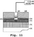
図11は、本発明の一実施形態に従って処理されている半導体基板の遷移点を決定する赤外線センサを有するCMPシステムの簡易化された概略図である。制御器164は検出器162を含む。制御器164は赤外線センサ166と通信する。赤外線センサはキャリヤプレート168内に含まれる。半導体基板172は、キャリヤプレート168内のキャリヤー膜170に対して支持される。赤外線センサ166は窓178を介して半導体基板172まで視界線(a line of view)を有する。研磨パッド174は半導体基板172の表面を平坦化する。研磨パッド174はステンレス鋼ベルト176の上に配置される。検出器162は赤外線センサに関連する傾斜ベース信号処理を閾値ベース信号に変換する。一実施形態では、図8A〜図8Cおよび図9を参照しながら記載したように、傾斜ベース信号は実信号と予測信号との間のデルタトレースを規定することによって閾値ベース作業に変換される。 FIG. 11 is a simplified schematic diagram of a CMP system having an infrared sensor for determining a transition point of a semiconductor substrate being processed according to an embodiment of the present invention. The controller 164 includes a
図12は、本発明の一実施形態に従って処理されている半導体基板の遷移点を決定するように構成された渦電流センサを有する処理システムの簡易化された概略図である。制御器164は検出器162を含む。制御器164は渦電流センサ180aおよび180bと通信する。渦電流センサ180aおよび180bは、半導体基板172の上に堆積される膜の厚さといった処理パラメータをモニターするように構成され得る。処理システムがCMP処理システムである場合、研磨パッド174は半導体基板172の表面を平坦化する。研磨パッド174はバッキング176の上に配置される。検出器162は、渦電流センサ180aおよび180bの傾斜ベース検出の出力を閾値検出処理に変換する。ここでもやはり検出器162は、遷移点を示す閾偏差値を検出するために計測値と予測値との差をトラックする。 FIG. 12 is a simplified schematic diagram of a processing system having an eddy current sensor configured to determine a transition point of a semiconductor substrate being processed according to an embodiment of the present invention. The controller 164 includes a
図11および図12は、半導体製造に用いられるセンサの特定の実施形態を描く。ここに記載された実施形態は、構成変化または状態変化をモニターすることが可能であるいかなるタイプのセンサとも結び付けられ得ることを理解されたい。例示的な構成変化は、第1の層が除去されて第2の層が露出されたり、半導体ウェーハといった物体の表面が改質されたりする表面の構造変化を含む。例示的な状態変化は、液体から気体へ、液体から固体へ等の変化を含む。実際、遷移点は構成変化または状態変化が生じる点と定義され得る。遷移点において、ここに記載されるセンサからモニターされる性質は処理条件が原因で変化する。ターゲットにされた性質は、厚さ、抵抗力、平面性、透過性、振動、化学成分等といった性質を含む。ここに記載されるように、この変化がモニターされて、遷移点が閾値検出スキームによって決定される。当業者は、ここに記載される実施形態が前述したセンサの特定のタイプに限られないことを理解する。特に、構成変化または状態変化を示す信号を検出するように構成された任意のセンサは、そのセンサが半導体製造処理と関連するかどうかにかかわらず、前述した実施形態に用いられ得る。さらに、センサは処理されている物体(例えば、半導体ウェーハ)または処理モジュールの構成要素(例えば、研磨パッド)の変化を検出し得ることを理解されたい。よって、遷移点は直接または間接的に検出され得る。いくつかの例示的なセンサは、抵抗、キャパシタンス、反射光、振動等を検出するように構成されたセンサを含む。 11 and 12 depict specific embodiments of sensors used in semiconductor manufacturing. It should be understood that the embodiments described herein can be combined with any type of sensor capable of monitoring configuration changes or state changes. Exemplary structural changes include structural changes in the surface where the first layer is removed and the second layer is exposed, or the surface of an object such as a semiconductor wafer is modified. Exemplary state changes include changes from liquid to gas, liquid to solid, and the like. In fact, transition points can be defined as points where configuration changes or state changes occur. At the transition point, the properties monitored from the sensors described herein change due to processing conditions. Targeted properties include properties such as thickness, resistance, planarity, permeability, vibration, chemical composition, and the like. As described herein, this change is monitored and the transition point is determined by a threshold detection scheme. Those skilled in the art will appreciate that the embodiments described herein are not limited to the specific types of sensors described above. In particular, any sensor configured to detect a signal indicative of a configuration change or state change may be used in the above-described embodiments regardless of whether the sensor is associated with a semiconductor manufacturing process. Further, it should be understood that the sensor may detect changes in an object being processed (eg, a semiconductor wafer) or a component of a processing module (eg, a polishing pad). Thus, the transition point can be detected directly or indirectly. Some exemplary sensors include sensors configured to detect resistance, capacitance, reflected light, vibration, and the like.
要約すれば、前述の発明は傾斜ベース検出タスクを閾値ベース検出タスクに変換する方法およびシステムを記載する。近似方程式(例えば、多項方程式)が現在のデータ点における期待値を予測するのに用いられる。センサから供給される期待値と対応する実際値との差がモニターされて、遷移点を検出する。モニターされた差は、ここに記載されるようにデルタトレースとして記録され得る。差をトラッキングすることによって、閾値が規定されることを可能にする。一実施形態では、遷移点は、事前に定義した数のモニターされた差の連続点がノイズ区域の外側で検出されるときに生じる。また、オフセットが、オフセット境界の外側で検出された点(すなわち、実際値と予測値との差の値)が遷移点を示すレベルを定義するのに提供され得る。傾斜検出タスクを閾値検出タスクに変換することによって、傾斜検出タスクに必要とされる微分係数を分析する必要性を避ける安定しかつ確実な遷移検出システムが提供される。さらに、前述したデルタトレースは、より容易に遷移点を識別するために遷移点で生じる変化を強化する。 In summary, the foregoing invention describes a method and system for converting a slope-based detection task into a threshold-based detection task. Approximate equations (eg, polynomial equations) are used to predict the expected value at the current data point. The difference between the expected value supplied from the sensor and the corresponding actual value is monitored to detect a transition point. The monitored difference can be recorded as a delta trace as described herein. By tracking the difference, a threshold can be defined. In one embodiment, a transition point occurs when a pre-defined number of monitored difference series are detected outside the noise zone. Also, an offset can be provided to define a level at which points detected outside the offset boundary (ie, the value of the difference between the actual value and the predicted value) indicate a transition point. By converting the slope detection task to a threshold detection task, a stable and reliable transition detection system is provided that avoids the need to analyze the derivative required for the slope detection task. Furthermore, the delta trace described above enhances the changes that occur at the transition points to more easily identify the transition points.
上記の実施形態を考慮して、本発明はコンピュータシステムに格納されるデータを含む種々のコンピュータによる実行作業を採用し得る。これら作業には、物理量の物理的操作を要求する作業が含まれる。通常、必ずしもではないが、これら量は、格納され、転送され、結合され、比較され、および他の方法で操作されることが可能である電気信号または磁気信号の形を取る。さらに、実行される操作はしばしば、生成、識別、決定または比較といった用語で呼ばれる。 In view of the above embodiments, the present invention may employ various computer execution operations including data stored in a computer system. These operations include operations that require physical manipulation of physical quantities. Usually, though not necessarily, these quantities take the form of electrical or magnetic signals capable of being stored, transferred, combined, compared, and otherwise manipulated. Furthermore, the operations performed are often referred to in terms of generation, identification, determination or comparison.
上記の発明は、手持形装置、マイクロプロセッサシステム、マイクロプロセッサベースまたはプログラマブル家庭用電化製品、ミニコンピュータ、メインフレームコンピュータ等を含む他のコンピュータシステム構成で実行され得る。本発明はまた、タスクが通信ネットワークを介してリンクされる遠隔処理装置によって実行される計算環境を配信するところで実行され得る。 The above invention may be practiced with other computer system configurations including handheld devices, microprocessor systems, microprocessor-based or programmable consumer electronics, minicomputers, mainframe computers and the like. The invention may also be practiced where a task is distributed in a computing environment where it is executed by a remote processing device linked via a communications network.
本発明はまた、コンピュータ読取可能媒体上のコンピュータ読取コードとしても具現化され得る。コンピュータ読取可能媒体は、その後コンピュータシステムによって読み取られ得るデータを格納することができる任意のデータ記憶装置である。コンピュータ読取可能媒体の例は、ハードドライブ、ネットワーク接続ストレージ(NAS)、読取り専用メモリ、ランダムアクセスメモリ、CD−ROM、CD−R、CD−RW、磁気テープおよび他の光学式および非光学式データストレージ装置を含む。コンピュータ読取可能媒体はまた、コンピュータシステムに連結されたネットワーク上で配信され得、その結果、コンピュータ読取可能コードは分散形方法で格納および実行される。 The present invention may also be embodied as computer readable code on a computer readable medium. The computer readable medium is any data storage device that can store data, which can thereafter be read by a computer system. Examples of computer readable media are hard drives, network attached storage (NAS), read only memory, random access memory, CD-ROM, CD-R, CD-RW, magnetic tape and other optical and non-optical data Includes storage devices. The computer readable medium may also be distributed over a network coupled to the computer system so that the computer readable code is stored and executed in a distributed fashion.
前記の本発明は明確な理解を目的に詳細に記載されてきたが、ある変化および修正が添付の請求項の範囲内で実行され得ることは明白である。従って、本実施形態は実例となるが限定的ではないと考えられる。また、本発明はここに与えられた詳細に限定されるものではなく、添付の請求項の範囲および同等物内で改良され得る。請求項では、要素および/またはステップは、請求項に明確に記載されていない限り、作業の特定の順番を意味するものではない。 Although the foregoing invention has been described in detail for purposes of clarity of understanding, it will be apparent that certain changes and modifications may be practiced within the scope of the appended claims. Thus, this embodiment is illustrative but not limiting. Also, the invention is not limited to the details given herein but may be modified within the scope and equivalents of the appended claims. In the claims, elements and / or steps do not imply any particular order of operation, unless explicitly stated in the claims.
本発明は概して、半導体製造に関し、特に半導体製造作業における処理とウェーハ状態モニタリングとのリアルタイム計測に関する。 The present invention relates generally to semiconductor manufacturing, and more particularly to real-time measurement of processing and wafer condition monitoring in semiconductor manufacturing operations.
(発明の背景)
半導体製造の間、下にある基板が形成、修正および様々な層の除去、ブランケットまたはパターン化の対象になるところには複数のステップが存在する。小さい特徴寸法、厳しい表面の平面性要求、スループットを上げることを絶え間なく探求することと相まって、処理された膜のターゲットにされた性質(厚さ、抵抗、平面性、透過性、化学成分等)が達成されたとき、すなわち、現在の工程ステップに対する終了点が得られたとき、工程パラメータを停止または変更することが強く所望される。もちろん、現在の工程ステップの後にその後の製造ステップに遷移する半導体製造ステップの中には、明確なウェーハ特徴を得るタスクを成し遂げているものがある。(Background of the Invention)
During semiconductor manufacturing, there are multiple steps where the underlying substrate is subject to formation, modification and removal of various layers, blankets or patterning. Targeted properties of the processed membrane (thickness, resistance, planarity, permeability, chemical composition, etc.) coupled with small feature dimensions, demanding surface flatness requirements, and continually seeking to increase throughput When is achieved, i.e., when an end point has been obtained for the current process step, it is highly desirable to stop or change the process parameters. Of course, some semiconductor manufacturing steps that transition to subsequent manufacturing steps after the current process step have accomplished the task of obtaining distinct wafer characteristics.
ウェーハ特徴を制御するリアルタイム計測は現在必要不可欠な存在であり、その結果、特定の処理作業の終了点または遷移点が決定され得る。半導体作業と関連するパラメータのin−situモニターは、処理作業の終了点または遷移点に関する有用な情報を提供する。通常、工程でウェーハに強く関連する物体(ウェーハ自体または他の物質)の性質は、遷移に先立って、および遷移の後に、単調量変化を経験し、遷移自体の間に急激な性質の変異を経る。これは、モニターされるシステムが十分に小さく、かつ、遷移が検査空間の観察点において同時に生じるときに、信号変動をモニターできるステップ状の性質をもたらす。より大きなシステム(例えば、半導体ウェーハ)については、ステップ状の遷移点を傾斜変化に移す時間分布がある。傾斜変化は、工程パラメータ変化に対応するデータ点に関連付けられ、終了点または遷移点の指標を生成する。しかしながら、傾斜変化検出は微分係数(derivative)の使用を必要とし、この微分係数はこのアプローチを複雑にする減少した信号対雑音比と関連する。Real-time metrology that controls wafer characteristics is now indispensable so that the end point or transition point of a particular processing operation can be determined. An in-situ monitor of parameters associated with the semiconductor operation provides useful information regarding the end or transition point of the processing operation. Typically, the nature ofan object (wafer itself or other substance) that is stronglyassociated with the wafer in the process will experiencea monotonic change prior toand after the transition,and abrupt changes in properties during the transition itself. afterRu. This system is monitored sufficientlyrather small, and,when the transition occurs simultaneouslyin the observation point of the examination space, resulting in a step-like characteristic thatcan monitor the signal change. Larger system (e.g., a semiconductor wafer) fortheRu timedistribution there to transfer the stepped transition point the slopechanges. The slope change is associated with a data point corresponding to the process parameter change and generates an end point or transition point indicator. However, slope change detection requires the use of a derivative, which is associated with a reduced signal-to-noise ratio that complicates the approach.
図1は、処理作業(例えば、平坦化処理作業)の間長期にわたってモニターされる半導体ウェーハの厚さに関するグラフである。線100は処理作業中の終了点/遷移点を決定する赤外線(IR)ベースのセンサに関連する値を表す。線102は、処理中の長期にわたる半導体ウェーハの厚さを記録する複数の渦電流センサ(ECS)に関連する値を表す。図に示すように、領域104は終了点/遷移点が生じる時間を表す。領域104では、一般傾斜は、複数の線102および線100の遷移と関連する。しかしながら、IRモニターまたは渦電流モニターのどちらか一方でモニターされている信号は、運転毎に変化する顕著なかつ可変性のバックグラウンドノイズと重畳される。従って、微分係数ベースの傾斜を計測することによって終了点を決定するとき、信号対雑音レベルは終了点決定の安定性と確実性とに影響する。よって、傾斜ベースの分析に予測される遷移点のインライン決定は、半導体作業に必要な確固たるデータを提供しない。FIG. 1 is a graph of semiconductor wafer thickness that is monitored over time during a processing operation (eg, a planarization processing operation).
そのため、従来技術の問題を解決し、モニターされる工程パラメータの傾斜ベースの遷移から遷移点が生じる工程のための、安定かつ確実な遷移点決定を提供する方法と装置とを提供する必要がある。Therefore, to solve the problems of the priorart,for the processof transition pointsarising from the transition of the gradient-based monitoredRu processparameters, it is necessary to provide a method of providing stable and reliable transition point determination apparatus and is there.
(発明の概要)
該して言えば、本発明は遷移点の決定の確実性と安定性とを向上させるために、微分係数ベースのデータを分析する必要性を排除し、かつ、閾値分析から遷移点の決定を可能にすることによってこれら必要性を満たす。本発明は、方法、システム、コンピュータ読取可能な媒体または装置として含む多数の方法で実行され得ることを理解されたい。本発明のいくつかの創意工夫に満ちた実施形態が以下に記載される。(Summary of Invention)
In other words, the present invention eliminates the need to analyze derivative-based data to improve the certainty and stability of transition point determination, and makes transition point determination from threshold analysis. It fulfills these needs by making it possible. It should be understood that the present invention can be implemented in numerous ways, including as a method, system, computer readable medium or device. Several inventive embodiments of the present invention are described below.
一実施形態では、傾斜ベース検出タスクを閾値ベース検出タスクに変換する方法が提供される。この方法は、モニターされている処理(process)の値に対応する一組の点の近似方程式を定義することから開始する。その後、モニターされている処理の現在の点における期待値が予測される。次に、モニターされている処理の現在の点における測定値と対応する期待値との間の差が計算される。それから、逐次点の差がモニターされることにより測定値と期待値との間の偏差量を検出する。次に、モニターされている処理の遷移点が偏差量の検出に基づいて識別される。In one embodiment, a method for converting a slope-based detection task into a threshold-based detection task is provided. The method begins by defining a set of point approximation equations that correspond to the values of the process being monitored. Thereafter, the expected value at the current point of the process being monitored is predicted. Next, the difference between the measured value at the current point of the process being monitored and the corresponding expected value is calculated. Then, the difference between successive points to detect adeviation between the expected and measured values by being monitored. Next, the transition point of the monitored process is identified based on the detection of the deviationamount .
別の実施形態では、傾斜ベース変化の遷移点を閾値検出から検出する方法が提供される。この方法は、遷移点と関連するパラメータをモニターすることから開始する。それから、パラメータの予測値がモニターされた処理パラメータの過去の値から計算される。予測値はモニターされている処理パラメータの現在値と対応する。次に、閾値が決定される。その後、現在値と予測値との間の差はトラックされる。次に、差が閾値を越えるとき、遷移点が識別される。In another embodiment, a method is provided for detecting a slope-based change transition point from threshold detection. The method begins by monitoring parameters associated with transition points. The predicted value of the parameter is then calculated from the past value of the monitored process parameter. The predicted valuecorresponds to the current value of the process parameter being monitored. Next, a threshold is determined. Thereafter, the difference between the current value and the predicted value is tracked. A transition point is then identified when the difference exceeds a threshold.
さらに別の実施形態では、傾斜変化遷移の遷移点をリアルタイムで閾値決定から検出することが可能である半導体処理システムが提供される。このシステムは、処理されている半導体ウェーハと関連する明確なパラメータが得られるまで半導体ウェーハを処理するように構成された処理モジュールを含む。処理システムは、処理作業に関連する処理パラメータをモニターするように構成されたセンタを含む。このシステムは、センサと通信する検出器を含む。この検出器は、測定値が傾斜変化から遷移点を示す場合、測定値を予測値と比較するように構成される。予測値はそれ以前に測定した値から導かれる。この検出器はさらに、測定値と対応する予測値との差をトラックすることにより、遷移点における変化を強化(enhance)し、閾偏差量が決定されることを可能にするように構成される。閾偏差量は処理作業に関連する遷移点を示す。In yet another embodiment, a semiconductor processing system is provided that can detect a transition point of a slope change transition from a threshold determination in real time. The system includes a processing module configured to process a semiconductor wafer until a defined parameter associated with the semiconductor wafer being processed is obtained. The processing system includes a center configured to monitor processing parameters associated with processing operations. The system includes a detector in communication with the sensor. The detector is configured to compare the measured value with a predicted value when the measured value indicates a transition point from a slope change. Predicted values are derived from previously measured values. The detector is further configured to enhance the change at the transition point and allow the threshold deviationamount to be determined by tracking the difference between the measured value and the corresponding predicted value. . The threshold deviationamount indicates a transition point related to the processing work.
さらにまた別の実施形態では、傾斜ベース検出タスクを閾値ベース検出タスクに変換するプログラム命令を有するコンピュータ読取可能な媒体が提供される。コンピュータ読取可能な媒体は、モニターされている処理の値に対応する一組の点の近似方程式を規定するプログラム命令と、モニターされている処理の現在点における期待値を予測するプログラム命令とを含む。モニターされている処理の現在点における計測値と対応する期待値との差を計算するプログラム命令が提供される。差をモニターすることにより、計測値と期待値との間の偏差量を検出するプログラム命令と、偏差量の検出に基づいてモニターされている処理の遷移点を識別するプログラム命令とが含まれる。In yet another embodiment, a computer readable medium having program instructions for converting a tilt based detection task into a threshold based detection task is provided. The computer-readable medium includes program instructions that define a set of approximate points corresponding to the value of the process being monitored, and program instructions that predict the expected value at the current point of the process being monitored. . Program instructions are provided for calculating the difference between the measured value at the current point of the monitored process and the corresponding expected value. By monitoring the difference, a program command for detecting a deviationamount between the measured value and the expected value and a program command for identifying a transition point of the process being monitored based on the detection of the deviationamount are included.
本発明の他の局面と利点とは、例として本発明の原理を説明する添付の図面と併せて以下の詳細な説明から明らかになる。
本発明は、添付の図面と併せて以下の詳細な説明によって容易に理解され、同様の参照番号は同様の構造要素を示す。Other aspects and advantages of the present invention will become apparent from the following detailed description, taken in conjunction with the accompanying drawings, illustrating by way of example the principles of the invention.
The present invention will be readily understood by the following detailed description in conjunction with the accompanying drawings, and like reference numerals designate like structural elements.
本発明は、半導体処理作業中、遷移点の確実かつ安定した測定を提供するシステム、装置および方法を示す。しかしながら、本発明はこれら特定の詳細のいくつかまたは全てをなしで実行され得ることは当業者にとって明らかである。別の場合では、よく知られた処理作業は本発明を不必要に分かりにくくしないために詳細に記載されていない。図1は(発明の背景)部分に記載される。 The present invention shows a system, apparatus and method that provides reliable and stable measurement of transition points during semiconductor processing operations. However, it will be apparent to those skilled in the art that the present invention may be practiced without some or all of these specific details. In other instances, well known process operations have not been described in detail in order not to unnecessarily obscure the present invention. FIG. 1 is described in the (Background of the invention) part.
本発明の実施形態は、傾斜検出タスクを閾値検出タスクに変換するシステムおよび方法、ならびに移転の標示である移転特徴を増幅するシステムおよび方法を提供する。閾値動作(threshold behavior)は、ゼロまたは定信号のバックグラウンドでステップ状の特徴を生成し、かつ、より単純なアルゴリズム、より高い信号対雑音比およびより確実な検出可能性を提供する。遷移点/終了点の閾値ベース決定は、傾斜ベース決定に比べてさらに高い安全性と確実性とを提供する。同様に、より安定したかつ確実なトリガリング条件が半導体作業に対して提供される。つまり、遷移点/終了点は高度な信頼度を持って決定されるので、実質的に正確な測定を要求する下流作業(downstream operation)がインライン計測から開始され得る。その結果、関連作業の半導体スループットが付随して増加され得る。微分係数分析に関する処理トレーシング信号の傾斜における小さい変化から生じる混乱は、トレーシング信号を閾値タイプに変換することによって除去される。ここで用いられる終了点および遷移点という用語は互換性があるということを理解されたい。ターゲット変化が生じている、ターゲット状態が達成される場合、またはモニターされるパラメータと関連するある値の到達が終了点または他の処理作業の開始といったイベントを開始させることに用いられる場合、終了点および遷移点という用語は半導体処理または他の処理における任意の点に関連し得ることは当業者にとって明白である。 Embodiments of the present invention provide a system and method for converting a tilt detection task to a threshold detection task, and a system and method for amplifying a transfer feature that is an indication of transfer. Threshold behavior generates a stepped feature with zero or constant signal background and provides a simpler algorithm, higher signal-to-noise ratio and more reliable detectability. Transition point / end point threshold-based determination provides even greater safety and certainty than slope-based determination. Similarly, more stable and reliable triggering conditions are provided for semiconductor operations. That is, since the transition point / end point is determined with a high degree of reliability, a downstream operation requiring substantially accurate measurement can be started from in-line measurement. As a result, the semiconductor throughput of related work can be increased concomitantly. Confusion resulting from small changes in the slope of the processed tracing signal for derivative analysis is eliminated by converting the tracing signal to a threshold type. It should be understood that the terms end point and transition point as used herein are interchangeable. An end point if a target change has occurred, a target state has been achieved, or the arrival of some value associated with a monitored parameter is used to initiate an event such as an end point or the start of another processing task It will be apparent to those skilled in the art that the terms and transition points may relate to any point in semiconductor processing or other processing.
図2は、赤外線(IR)ベースのトレースに関するグラフであり、ここで遷移領域におけるノイズレベルは本発明の一実施形態に従って遷移点を示すようにスムーズ化される。ここで、領域106において、トレース108がスムーズ化された線として示されるように、ノイズレベルは実質的に除去される。図に示すように、傾斜は領域106におけるスムーズ化されたトレース108遷移と一体になった。しかしながら、モニターされている作業(例えば、化学機械的平坦化(CMP)作業またはエッチング作業)と関連するノイズは、リアルタイムの安定したかつ再現性のある読取りが終了点または他の作業の開始といったイベントを開始させることを妨げる。図2は温度に関連する赤外線信号を説明するが、他の信号、例えば渦電流センサ、振動、光学屈折等は同様の性質を示すことを理解されたい。つまり、スムーズ化された傾斜は遷移点を示す。しかしながら、前述したように、バックグラウンドノイズは、安定したかつ正確なリアルタイム読取りが、傾斜読取りすることを防ぐ。以下により詳細に説明されるように、傾斜測定を閾値測定に変換することにより、傾斜測定と関連する微分係数測定のために分析される小さい差に影響を与えるノイズレベルに関連する不確実性を、除去する。よって、リアルタイムにおいて遷移点をはるか正確に検出することが可能になる。遷移点を示す傾斜における小さい変化は、傾斜測定のノイズによって遮蔽される。しかしながら、ここで記載される実施形態は、実質的にノイズを除去することにより、遷移点の決定に影響を与えない。FIG. 2 is a graph for an infrared (IR) based trace, where the noise level in the transition region is smoothed to indicate a transition point according to one embodiment of the present invention. Here, in
図3は、長期にわたる信号トレースに関する例示的なグラフであり、ここで、時間の期間は遷移点を含む。ここで、信号110は長期にわたってプロットされる。一実施形態では、信号110は処理パラメータを検出するように構成された渦電流センサからもたらされ、半導体作業中の遷移点を示す。半導体作業中の遷移点を検出する他の信号(例えば、赤外線、振動、光学ベースの信号等)はここに含まれ得ることを理解されたい。図に示すように、信号110は信号に関連する相当量のノイズを有しているが、長期にわたる傾向が時間100における遷移点を示す。当業者は、傾斜ベースの決定ではバックグラウンドノイズが原因でここでは不安定な結果を生み出すことを理解する。 FIG. 3 is an exemplary graph for signal traces over time, where the time period includes transition points. Here, signal 110 is plotted over time. In one embodiment, signal 110 is derived from an eddy current sensor configured to detect a processing parameter and indicates a transition point during semiconductor operation. It should be understood that other signals that detect transition points during semiconductor operation (eg, infrared, vibration, optical based signals, etc.) may be included here. As shown, signal 110 has a significant amount of noise associated with the signal, but a long-term trend indicates a transition point at
図4は、スムーズ化されてノイズを除去した図3の信号に関する例示的なグラフである。ここで、線110aは、信号をスムーズ化するために、通常の正弦ノイズフィルターが適用された。信号110aが長期にわたる渦電流センサの値を表す場合には、遷移点は、ほぼ時間100における傾斜の変化によって示される。前述したように、スムーズ化された傾斜は、リアルタイムで安定したかつ正確な方法で生成されることができない。従って、傾斜ベースの決定はここでは実行可能な代案ではない。FIG. 4 is an exemplary graph for the signal of FIG. 3 that has been smoothed to remove noise. Here, the
図5は、本発明の一実施形態に従って図3の実際の信号の点から生成された予測された信号に関する例示的なグラフである。ここでは、選択した区間のデータフロー点の近似方程式を用いて、本発明の一実施形態の最近のデータ読取りを予測する。図8Aと図8Bとを参照しながらより詳細に説明されるように、予測信号は、本発明の一実施形態に従って近似方程式を実信号の履歴データ点に適用して、予測されたリアルタイムデータ点を生成することによって生成される。図5に示されるように、線110bによって表される予測信号は、遷移点を表す時間100において、図3および図4の実信号から逸脱し始める。近似方程式は任意の多項方程式であり得ることを理解されたい。例えば、近似方程式は一次方程式、放物線型方程式または他のより高い累乗の方程式の形式をとり得る。 FIG. 5 is an exemplary graph for a predicted signal generated from the actual signal points of FIG. 3 in accordance with one embodiment of the present invention. Here, an approximate equation of the data flow point of the selected interval is used to predict the recent data reading of an embodiment of the present invention. As will be described in more detail with reference to FIGS. 8A and 8B, the predicted signal can be estimated by applying an approximation equation to the historical data points of the real signal in accordance with one embodiment of the present invention. Is generated by generating As shown in FIG. 5, the predicted signal represented by
図6は、本発明の一実施形態に従って、様々な時間点における実信号と対応する予測信号との差を計算することによって生成された偏差信号に関する例示的なグラフである。ここで、線112は長期にわたる予測信号と実信号との差を表す。領域114はノイズ区域(corridor of noise)を現す。つまり、実信号と予測信号との差にオフセットが適用されることによりノイズ区域を規定することができ、ここで、ノイズ区域の外側にある点は遷移点として妥当な点であると考えられる。本質的に、ノイズ区域は実際値と予測値との差の周りに境界を規定する。一実施形態において、オフセットは標準偏差の3倍(すなわち、3σ)に設定される。よって、ノイズ分布がガウス分布のように構成される場合、3σは分布における全ての点のうち99.7%をカバーする。したがって、1000点のうち、ノイズ区域の外側に実際あり、遷移点の開始点ではない一点に対する確率は3×10⁻³である。モニターされている処理の性質次第で、この確率は減少または増加して許容されるレベルの正確さを提供し得る。FIG. 6 is an exemplary graph for a deviation signal generated by calculating a difference between a real signal and a corresponding predicted signal at various time points in accordance with an embodiment of the present invention. Here,
図7は、本発明の一実施形態に従って、互いに重畳された図4、図5および図6のグラフを含む例示的なグラフであり、遷移点の閾値決定を明らかにする。ここでは、図4からの線110a、図5からの線110bおよび線112が互いに重畳されている。さらに、ノイズ区域114も示されている。偏差信号、すなわち、実信号と予測信号との差を表す線112は、時間100の遷移点においてノイズ区域を超え始めることが理解されたい。以下により詳細に説明されるように、(ノイズの)3σ区域は遷移点が検出されているというより高いまたはより低い信頼水準を与えるために調整され得る。例えば、高度な正確度および精密度を要求する処理は、より低い程度の正確度および精密度を要求する処理よりも広いノイズ区域を使用し得る。他の実施形態では、ノイズ区域の境界の外側に1つ以上の連続点が遷移点を認めることを開始するのに要求され得る。FIG. 7 is an exemplary graph including the graphs of FIGS. 4, 5 and 6 superimposed on each other, in accordance with one embodiment of the present invention, demonstrating transition point threshold determination. Here, the
図8Aは、本発明の一実施形態に従う実信号と予測信号とのトレースを示す例示的なグラフである。線120は、長期にわたる処理パラメータ読取りのプロットを表す。処理パラメータは一実施形態において膜の厚さと関連する処理パラメータであることを理解されたい。グラフの領域121は遷移前の領域を表し、他方でグラフの領域123は遷移後の領域を表す。よって、線120は2つの連続的な処理(例えば、遷移前領域の処理および遷移後領域の処理)を表しており、2つの処理の間には遷移点という形で割込みがある。遷移点はここで1つの状態から他の状態への変化を示す。ここで記載された実施形態は半導体処理を参照するが、この方法論は遷移が生じており、傾斜検出処理が1つの状態から他の状態への遷移を記録し得る場合の任意のシステムに適用され得ることを理解されたい。FIG. 8A is an exemplary graph illustrating traces of real and predicted signals according to one embodiment of the present invention.
今なお図8Aを参照して、前区分またはデータ区間(例えば、領域121の区分n)は後の時間点における値を予測するのに用いられる。一実施形態では、多項方程式(例えば、放物線型方程式)を用いて、最近のデータ読取りに対応する予測値を導く。ここで、データの区分(データ区間とも呼ばれる)を取って、距離mから与えられるデータ値が計算される。当業者は、一実施形態において、データ値を出すのに用いられる放物線型(またはより高い累乗)の近似は、Y=a1tn+a2tn-1...+anの形式であることを理解する。ここで、Yは予測値(y座標の値)を表しており、tは時間(x座標の値)を表している。もちろんここでは、以前のデータはそのデータが関連するそれぞれの領域のダイナミクスを表していると仮定される。Still referring to FIG. 8A, the previous section or data interval (eg, section n of region 121) is used to predict a value at a later time point. In one embodiment, a polynomial equation (eg, a parabolic equation) is used to derive a predicted value corresponding to a recent data reading. Here, taking a data section (also called a data section), a data value given from the distance m is calculated. One skilled in the art will recognize that in one embodiment, the parabolic (or higher power) approximation used to generate the data values is Y = a1 tn + a2 tn−1 . . . + Understand that in the form of an. Here, Y represents a predicted value (y-coordinate value), and t represents time (x-coordinate value). Of course, here it is assumed that the previous data represents the dynamics of the respective region to which the data relates.
よって、検出装置(すなわち、センサ)によって測定される実信号は、近似方程式から計算される予測信号と比較され得る。実信号と予測信号とは、遷移が生じない限り、かつ、推定(外挿)の距離が大きすぎない限り、実質的に等しい。つまり、実信号の値と予測信号の値との差(Si−Yと表され、ここでSiは実信号でありYは予測信号である)はノイズレベル内で0に近い。しかしながら、遷移が生じると、図8AのΔ122で表されるように、実信号と予測値との差は0より徐々に大きくなり始める(Si−Y>0)。従って、閾値は実信号と予測値とが逸脱するところを検出するのに用いられ得る。後にさらに説明されるように、傾斜検出処理を閾値検出処理に変換することは、遷移に関連する変化を強化(増幅)し、その結果、遷移がより正確にかつ精密に識別され得る。Thus, the actual signal measured by the detector (ie, sensor) can be compared with the predicted signal calculated from the approximate equation. The actual signal and the predicted signal, as long as the transition does not occur, and theestimated unless too largedistance(extrapolation), are substantially equal. That is, the difference between the actual signal value and the predicted signal value (expressed as Si-Y, where Si is the actual signal and Y is the predicted signal) isclose to 0 within the noise level. However, when the transitionoccurs, as represented by Δ122 in FIG. 8A, the difference between the predicted and actual signal graduallythat started becomes greater than 0 (Si-Y> 0) .Thus, thethreshold can be used to detect the place where the actual signal and the predicted value deviates.As described further below, converting the tilt detection process to a threshold detection process enhances (amplifies) changes associated with the transition so that the transition can be more accurately and precisely identified.
図8Bは、本発明の一実施形態に従って、最初の信号値に関するグラフと、実信号と予測信号との間の偏差に関する対応するグラフとである。図8Bの上のグラフは、図8Aの実信号を表す。例えば、半導体処理モニタリングに関して、線120は赤外線センサ、渦電流センサ、振動センサ、温度センサ、反射スペクトルを検出するように構成されたセンサ等からの信号と関連するトレースを表し得る。時間ttにおいて生じる遷移は偏差トレース128(デルタトレースとも呼ばれる)から検出される。領域124と領域126とは、予測値が実信号からそれぞれ正の差と負の差として実信号から逸脱する領域を表す。FIG. 8B is a graph for the initial signal value and a corresponding graph for the deviation between the real signal and the predicted signal, in accordance with one embodiment of the present invention. The upper graph of FIG. 8B represents the real signal of FIG. 8A. For example, for semiconductor processing monitoring,
図8Bのデルタトレース128は、長期にわたる実信号と予測信号との差を表す。領域114はノイズ区域を表す。デルタトレース128および実信号のトレース120は各トレースに関連するバックグラウンドノイズを有する可能性があることを理解されたい。従って、トレース120は図3のトレースに類似する可能性があり、デルタトレース128は図6のトレースに類似する可能性がある。つまり、トレースはスムーズな線であるよりもむしろ、各トレースに関連するノイズを有する可能性がある。従って、ノイズ区域はノイズレベルを考慮に入れるように構成され、その結果、ノイズレベルは遷移点の決定に影響を与えない。同時に、大きさ(ノイズ区域のオフセットに関連して)が選ばれ、その結果、遷移がノイズレベルを超えて生じ、つまり、ノイズ区域が遷移点を遮蔽するほど大きくない。 The
一実施形態では、ノイズ区域のオフセットはデルタトレース128の3倍標準偏差(3σ)に設定される。よって、ノイズがガウス分布である場合、3σは分布の全ての点のうち99.7%をカバーする。前述したように、ノイズ区域の外側にあり、遷移点の開始点ではない一点に対して3×10⁻³の確率があり、各1000個の点のうち3つの点が実際に規定された3σ区間の外側にあり得ることを意味している。図9を参照しながらさらに説明されるように、遷移点発生に関する誤った判断の可能性を減らすために、遷移点の開始を示すものとして、ノイズ区域の外側にある多数の連続点が、要求され得る。一実施形態において、ノイズ区域の外側の適度に多数の連続点が用いられる場合、または3σより大きいノイズ区域が用いられる場合、オフセットは必ずしも必要ではない。ノイズ区域の外側にあるいずれの数の連続点も、遷移点のトリガーとして定義され得ることを理解されたい。遷移点に達したことを示すのに必要とされる連続点の数が高ければ高いほど、実遷移点が得られたという信頼度がより強い。よって、誤判断が高コストにつき、回復不能な損傷を引き起こす、正確さの要求される作業においては、高度な信頼度を提供するため、ノイズ区域の外側の3つ以上の連続点が選ばれ得る。作業がそれほど厳しくない場合、3つの点より少ない点を選ぶことが望ましいであろう。In one embodiment, the noise zone offset is set to three times the standard deviation (3σ ) of the
図8Cは、図8Aおよび図8Bの実トレースとデルタトレースとを示すグラフであり、予測値トレースが重畳されており、これら全ては傾斜ベースタスクを閾値ベースタスクに本発明の一実施形態に従って変換する際に使用される。トレース120は実センサ読取りを表す。トレース136は放物線状に外挿した予測値を表す。トレース128は、実センサ読取りと対応する予測値との差であるデルタトレースを表す。放物線状に外挿した予測値は、データ点の選択した区間と関連する放物線近似と、最先のデータ読取りの放物線予測とを含む。デルタトレース128は、現在点と多数の先行する連続点について、放物線状に外挿した予測値を減算することによって、計算される。よって、閾値は、デルタトレースがしっかりとノイズレベルを超えているときに、定められ得る。例えば、遷移点が生じたことを確認するのに先立って、ノイズレベルの外にある多数の連続点を規定することは、遷移点決定が正確であるという高い信頼度レベルを提供する。当業者は、遷移点がここで用いられる終了点を含むことを理解する。放物線型方程式がこの実施形態において近似方程式として用いられているが、任意の多項方程式が近似方程式として用いられ得、それは実センサ読取りによって規定される曲線の形が近似方程式の型に影響を与えるからであることを理解されたい。FIG. 8C is a graph showing the actual and delta traces of FIGS. 8A and 8B with superimposed predictor traces, all of which convert slope-based tasks to threshold-based tasks according to one embodiment of the present invention. Used when doing.
図3および図6を参照すれば、図6のデルタトレースアプローチの閾値決定が図3の傾斜ベースのアプローチよりも優れていることが分かる。つまり、傾斜ベースの決定におけるノイズは、傾斜の小さい変化を隠すが、閾値ベースの決定におけるノイズは、遷移点の認知を開始するのに先だってオフセットを規定することによって、またはノイズ区域の外側にある多数の連続点を要求することによって、関心事としては排除される。遷移点が達成されると、他の所定の作業が開始し得、または現在の作業の終了点が生じ得ることを理解されたい。半導体製造(例えば、エッチング、堆積、CMP作業または他の表面改質処理)に関して、第1の層は追加、除去、平坦化または改質され得、その後半導体ウェーハはこの処理ツールまたは異なる処理ツールで別のモジュールに遷移され得る。Referring to FIGS. 3 and 6, it can be seen that threshold determination of the delta trace approach of Figure 6 is superior than the slope based approach of Figure 3. That is, noise in the determination of the inclinedbase, which hides small changesin slope, noise in the determination of the threshold-based, by definingprior offsetto initiate recognition of the transition point or is outside the noise zone By requiring a large number of consecutive points, itis eliminated as a concern. It should be understood that once the transition point is achieved, other predetermined tasks may begin or end points of the current task may occur. For semiconductor manufacturing (eg, etching, deposition, CMP operations or other surface modification processes), the first layer can be added, removed, planarized, or modified, after which the semiconductor wafer is processed with this processing tool or a different processing tool. It can be transitioned to another module.
図9は、本発明の一実施形態に従って、傾斜ベース検出タスクを閾値ベース検出タスクに変換する方法についての方法作業に関するフローチャートである。この方法は作業140で開始し、ここで近似方程式が一組の点について規定される。一組の点に対する近似方程式は、モニターされている処理の値に対応する。例えば、多項方程式(例えば、放物線型方程式)は前述したように近似方程式であり得る。モニターされている処理は、渦電流センサ、赤外線センサ、温度センサ、振動センサ等からモニターされ得る。この方法はそれから作業142に進み、ここでモニターされている処理の現在点における期待値が予測される。ここで、多項方程式が多数の連続点のデータ区分を取り、現在点の期待値を予測する。本質的には、多項方程式は図8Aを参照しながら記載したように、現在点を過去のデータ点から予測することを可能にする。 FIG. 9 is a flow chart for method operations for a method of converting a slope-based detection task into a threshold-based detection task, according to one embodiment of the invention. The method begins at
図9の方法はそれから作業144に進み、ここで処理の現在点における測定された(実際の)値と対応する期待値との差が計算される。ここで、測定値と期待(予測)値との差は遷移点までほぼ0である。この差は2つの値の間の減算という点から測定され得るが、差の観察はこれに限られないことを理解されたい。差は図8A〜図8Cを参照しながら前述したように、デルタトレースとして記録され得る。よって、処理の現在点における測定値と対応する期待値との差は、作業146においてモニターされて、偏差量が検出される。偏差量はノイズ区域の外側にある多数の連続点として規定され得、ここで連続点の数は1以上でありえる。他の実施形態では、差はまた比、差の平方等としても計算され得る。つまり、ここで用いられる差という用語は、2つの値の一般化された差を示す広範囲な尺度に関連する。あるいは、オフセットが用いられ得、ここでオフセットはバックグラウンドノイズが遷移点を示すことを避けるように十分高く、かつ、遷移点を示す偏差量が識別され得る(すなわち、オフセットによって遮蔽されない)ように十分低い。方法はそれから作業148に進み、ここでモニターされている処理の遷移点が偏差量の検出に基づいて識別される。もちろん、遷移点は現在の処理作業を終了して別の処理作業を開始させるか、もしくは単に現在の処理を終了し得る。The method of FIG. 9 then proceeds to operation 144 where the difference between the measured (actual) value at the current point of processing and the corresponding expected value is calculated. Here, the difference between the measured value and the expected (predicted) value is almost zero until the transition point. It should be understood that although this difference can be measured in terms of subtraction between two values, the observation of the difference is not limited to this. The difference may be recorded as a delta trace, as described above with reference to FIGS. 8A-8C. Therefore, the difference between the corresponding expected value and the measured value at the current point of the process, is monitored in the working146,deviationis discovered. Theamount of deviationcan be defined as a number of consecutive points outside the noise zone, where the number of consecutive points can be one or more. In other embodiments, the difference may also be calculated as a ratio, a square of the difference, etc. That is, the term difference as used herein relates to a wide range of measures that indicate a generalized difference between two values. Alternatively, an offset can be used, where the offset is high enough to avoid background noise indicating a transition point, and theamount of deviation indicating the transition point can be identified (ie, not masked by the offset). Low enough. The method then proceeds to
図10は、本発明の一実施形態に従って、傾斜検出遷移点を閾値検出遷移点に変換するように構成された検出器と通信する処理モジュールの高水準の概略図である。処理モジュール160は、任意の処理モジュールであり得、例えば、CMPモジュール、エッチングモジュール等といった半導体関連の処理モジュールであり得る。検出器162は処理モジュール160と通信する。例えば、処理モジュール160内に位置するセンサを用いて、検出器162に信号を転送し得る。検出器162は、傾斜が遷移点を決定する処理を、閾値を用いて遷移点を検出する閾値検出処理に変換するように構成される。つまり、図8A、図8B、図8Cおよび図9を参照しながら記載された傾斜検出処理を閾値検出処理に変換する実施形態は検出器162によって行われる。さらに、遷移点において発生する変化が強化され、その結果、閾値が容易に検出され得る。一実施形態において、閾値は、ここで記載されるように実信号と予測信号との差と定義される。検出器162は、処理モジュール160において実行されている処理作業を制御する汎用コンピュータであり得ることを理解されたい。検出器162は、以下に記載されるように構成変化または状態変化をモニターするように構成されたセンサから信号を受信し得る。もちろん、処理モジュール160と検出器162との間の通信は閉ループを介し得る。 FIG. 10 is a high-level schematic diagram of a processing module in communication with a detector configured to convert a tilt detection transition point to a threshold detection transition point, according to one embodiment of the present invention. The
図11は、本発明の一実施形態に従って処理されている半導体基板の遷移点を決定する赤外線センサを有するCMPシステムの簡易化された概略図である。制御器164は検出器162を含む。制御器164は赤外線センサ166と通信する。赤外線センサはキャリヤプレート168内に含まれる。半導体基板172は、キャリヤプレート168内のキャリヤー膜170に対して支持される。赤外線センサ166は窓178を介して半導体基板172まで視界線(a line of view)を有する。研磨パッド174は半導体基板172の表面を平坦化する。研磨パッド174はステンレス鋼ベルト176の上に配置される。検出器162は赤外線センサに関連する傾斜ベース信号処理を閾値ベース信号に変換する。一実施形態では、図8A〜図8Cおよび図9を参照しながら記載したように、傾斜ベース信号は実信号と予測信号との間のデルタトレースを規定することによって閾値ベース作業に変換される。 FIG. 11 is a simplified schematic diagram of a CMP system having an infrared sensor for determining a transition point of a semiconductor substrate being processed according to an embodiment of the present invention. The controller 164 includes a
図12は、本発明の一実施形態に従って処理されている半導体基板の遷移点を決定するように構成された渦電流センサを有する処理システムの簡易化された概略図である。制御器164は検出器162を含む。制御器164は渦電流センサ180aおよび180bと通信する。渦電流センサ180aおよび180bは、半導体基板172の上に堆積される膜の厚さといった処理パラメータをモニターするように構成され得る。処理システムがCMP処理システムである場合、研磨パッド174は半導体基板172の表面を平坦化する。研磨パッド174はバッキング176の上に配置される。検出器162は、渦電流センサ180aおよび180bの傾斜ベース検出の出力を閾値検出処理に変換する。ここでもやはり検出器162は、遷移点を示す閾偏差量を検出するために計測値と予測値との差をトラックする。FIG. 12 is a simplified schematic diagram of a processing system having an eddy current sensor configured to determine a transition point of a semiconductor substrate being processed according to an embodiment of the present invention. The controller 164 includes a
図11および図12は、半導体製造に用いられるセンサの特定の実施形態を描く。ここに記載された実施形態は、構成変化または状態変化をモニターすることが可能であるいかなるタイプのセンサとも結び付けられ得ることを理解されたい。例示的な構成変化は、第1の層が除去されて第2の層が露出されたり、半導体ウェーハといった物体の表面が改質されたりする表面の構造変化を含む。例示的な状態変化は、液体から気体へ、液体から固体へ等の変化を含む。実際、遷移点は構成変化または状態変化が生じる点と定義され得る。遷移点において、ここに記載されるセンサからモニターされる性質は処理条件が原因で変化する。ターゲットにされた性質は、厚さ、抵抗力、平面性、透過性、振動、化学成分等といった性質を含む。ここに記載されるように、この変化がモニターされて、遷移点が閾値検出スキームによって決定される。当業者は、ここに記載される実施形態が前述したセンサの特定のタイプに限られないことを理解する。特に、構成変化または状態変化を示す信号を検出するように構成された任意のセンサは、そのセンサが半導体製造処理と関連するかどうかにかかわらず、前述した実施形態に用いられ得る。さらに、センサは処理されている物体(例えば、半導体ウェーハ)または処理モジュールの構成要素(例えば、研磨パッド)の変化を検出し得ることを理解されたい。よって、遷移点は直接または間接的に検出され得る。いくつかの例示的なセンサは、抵抗、キャパシタンス、反射光、振動等を検出するように構成されたセンサを含む。 11 and 12 depict specific embodiments of sensors used in semiconductor manufacturing. It should be understood that the embodiments described herein can be combined with any type of sensor capable of monitoring configuration changes or state changes. Exemplary structural changes include structural changes in the surface where the first layer is removed and the second layer is exposed, or the surface of an object such as a semiconductor wafer is modified. Exemplary state changes include changes from liquid to gas, liquid to solid, and the like. In fact, transition points can be defined as points where configuration changes or state changes occur. At the transition point, the properties monitored from the sensors described herein change due to processing conditions. Targeted properties include properties such as thickness, resistance, planarity, permeability, vibration, chemical composition, and the like. As described herein, this change is monitored and the transition point is determined by a threshold detection scheme. Those skilled in the art will appreciate that the embodiments described herein are not limited to the specific types of sensors described above. In particular, any sensor configured to detect a signal indicative of a configuration change or state change may be used in the above-described embodiments regardless of whether the sensor is associated with a semiconductor manufacturing process. Further, it should be understood that the sensor may detect changes in an object being processed (eg, a semiconductor wafer) or a component of a processing module (eg, a polishing pad). Thus, the transition point can be detected directly or indirectly. Some exemplary sensors include sensors configured to detect resistance, capacitance, reflected light, vibration, and the like.
要約すれば、前述の発明は傾斜ベース検出タスクを閾値ベース検出タスクに変換する方法およびシステムを記載する。近似方程式(例えば、多項方程式)が現在のデータ点における期待値を予測するのに用いられる。センサから供給される期待値と対応する実際値との差がモニターされて、遷移点を検出する。モニターされた差は、ここに記載されるようにデルタトレースとして記録され得る。差をトラッキングすることによって、閾値が規定されることを可能にする。一実施形態では、遷移点は、事前に定義した数のモニターされた差の連続点がノイズ区域の外側で検出されるときに生じる。また、オフセットが、オフセット境界の外側で検出された点(すなわち、実際値と予測値との差の値)が遷移点を示すレベルを定義するのに提供され得る。傾斜検出タスクを閾値検出タスクに変換することによって、傾斜検出タスクに必要とされる微分係数を分析する必要性を避ける安定しかつ確実な遷移検出システムが提供される。さらに、前述したデルタトレースは、より容易に遷移点を識別するために遷移点で生じる変化を強化する。 In summary, the foregoing invention describes a method and system for converting a slope-based detection task into a threshold-based detection task. Approximate equations (eg, polynomial equations) are used to predict the expected value at the current data point. The difference between the expected value supplied from the sensor and the corresponding actual value is monitored to detect a transition point. The monitored difference can be recorded as a delta trace as described herein. By tracking the difference, a threshold can be defined. In one embodiment, a transition point occurs when a pre-defined number of monitored difference series are detected outside the noise zone. Also, an offset can be provided to define a level at which points detected outside the offset boundary (ie, the value of the difference between the actual value and the predicted value) indicate a transition point. By converting the slope detection task to a threshold detection task, a stable and reliable transition detection system is provided that avoids the need to analyze the derivative required for the slope detection task. Furthermore, the delta trace described above enhances the changes that occur at the transition points to more easily identify the transition points.
上記の実施形態を考慮して、本発明はコンピュータシステムに格納されるデータを含む種々のコンピュータによる実行作業を採用し得る。これら作業には、物理量の物理的操作を要求する作業が含まれる。通常、必ずしもではないが、これら量は、格納され、転送され、結合され、比較され、および他の方法で操作されることが可能である電気信号または磁気信号の形を取る。さらに、実行される操作はしばしば、生成、識別、決定または比較といった用語で呼ばれる。 In view of the above embodiments, the present invention may employ various computer execution operations including data stored in a computer system. These operations include operations that require physical manipulation of physical quantities. Usually, though not necessarily, these quantities take the form of electrical or magnetic signals capable of being stored, transferred, combined, compared, and otherwise manipulated. Furthermore, the operations performed are often referred to in terms of generation, identification, determination or comparison.
上記の発明は、手持形装置、マイクロプロセッサシステム、マイクロプロセッサベースまたはプログラマブル家庭用電化製品、ミニコンピュータ、メインフレームコンピュータ等を含む他のコンピュータシステム構成で実行され得る。本発明はまた、タスクが通信ネットワークを介してリンクされる遠隔処理装置によって実行される計算環境を配信するところで実行され得る。 The above invention may be practiced with other computer system configurations including handheld devices, microprocessor systems, microprocessor-based or programmable consumer electronics, minicomputers, mainframe computers and the like. The invention may also be practiced where a task is distributed in a computing environment where it is executed by a remote processing device linked via a communications network.
本発明はまた、コンピュータ読取可能媒体上のコンピュータ読取コードとしても具現化され得る。コンピュータ読取可能媒体は、その後コンピュータシステムによって読み取られ得るデータを格納することができる任意のデータ記憶装置である。コンピュータ読取可能媒体の例は、ハードドライブ、ネットワーク接続ストレージ(NAS)、読取り専用メモリ、ランダムアクセスメモリ、CD−ROM、CD−R、CD−RW、磁気テープおよび他の光学式および非光学式データストレージ装置を含む。コンピュータ読取可能媒体はまた、コンピュータシステムに連結されたネットワーク上で配信され得、その結果、コンピュータ読取可能コードは分散形方法で格納および実行される。 The present invention may also be embodied as computer readable code on a computer readable medium. The computer readable medium is any data storage device that can store data, which can thereafter be read by a computer system. Examples of computer readable media are hard drives, network attached storage (NAS), read only memory, random access memory, CD-ROM, CD-R, CD-RW, magnetic tape and other optical and non-optical data Includes storage devices. The computer readable medium may also be distributed over a network coupled to the computer system so that the computer readable code is stored and executed in a distributed fashion.
前記の本発明は明確な理解を目的に詳細に記載されてきたが、ある変化および修正が添付の請求項の範囲内で実行され得ることは明白である。従って、本実施形態は実例となるが限定的ではないと考えられる。また、本発明はここに与えられた詳細に限定されるものではなく、添付の請求項の範囲および同等物内で改良され得る。請求項では、要素および/またはステップは、請求項に明確に記載されていない限り、作業の特定の順番を意味するものではない。 Although the foregoing invention has been described in detail for purposes of clarity of understanding, it will be apparent that certain changes and modifications may be practiced within the scope of the appended claims. Thus, this embodiment is illustrative but not limiting. Also, the invention is not limited to the details given herein but may be modified within the scope and equivalents of the appended claims. In the claims, elements and / or steps do not imply any particular order of operation, unless explicitly stated in the claims.
Claims (18)
Translated fromJapaneseモニターされている処理の値に従って一組の点の近似方程式を規定することと、
該モニターされている処理の現在点における期待値を予測することと、
該モニターされている処理の該現在点における測定値と該対応する期待値との差を計算することと、
該差をモニターすることにより、該測定値と該期待値との間の偏差値を検出することと、
該偏差値の該検出に基づいて該モニターされている処理の遷移点を識別することと
を包含する、方法。A method for converting a slope-based detection task into a threshold-based detection task, comprising:
Defining an approximate equation for a set of points according to the value of the process being monitored;
Predicting the expected value at the current point of the monitored process;
Calculating the difference between the measured value at the current point of the monitored process and the corresponding expected value;
Detecting a deviation value between the measured value and the expected value by monitoring the difference;
Identifying a transition point of the monitored process based on the detection of the deviation value.
ノイズ区域を規定することであって、該ノイズ区域は境界を提供し、前記偏差値は該境界の外側に収まる、ことと
をさらに包含する、請求項1に記載の方法。Tracing the difference between the measured value and the corresponding expected value;
The method of claim 1, further comprising: defining a noise zone, wherein the noise zone provides a boundary, and the deviation value falls outside the boundary.
処理されている半導体ウェーハと関連する定義済みパラメータが得られるまで該半導体ウェーハを処理するように構成された処理モジュールであって、処理作業と関連する処理パラメータをモニターするように構成されたセンサを含む処理モジュールと、
該センサと通信する検出器であって、該検出器は測定値を予測値と比較するように構成されており、該測定値は傾斜変化から遷移点を示しており、該予測値は以前に測定された値から導かれており、該検出器はさらに該測定値と該対応する予測値との差をトラックすることにより該遷移点における変化を強化し、閾偏差値が規定されることを可能にし、該閾偏差値は該処理作業と関連する該遷移点を示す、検出器と
を備える、システム。A semiconductor processing system capable of detecting a transition point of a slope change transition from a threshold value determination in real time,
A processing module configured to process a semiconductor wafer until a predefined parameter associated with the semiconductor wafer being processed is obtained, wherein the sensor is configured to monitor the processing parameter associated with the processing operation. Including processing modules;
A detector in communication with the sensor, the detector configured to compare the measured value with a predicted value, the measured value indicating a transition point from a slope change, the predicted value previously Deduced from the measured value, the detector further tracks the difference between the measured value and the corresponding predicted value to enhance the change at the transition point, and a threshold deviation value is defined. And a detector, wherein the threshold deviation value indicates the transition point associated with the processing operation.
モニターされている処理の値に対応する一組の点についての近似方程式を規定するプログラム命令と、
該モニターされている処理の現在点における期待値を予測するプログラム命令と、
該モニターされている処理の該現在点における測定値と該対応する期待値との差を計算するプログラム命令と、
該差をモニターすることにより該測定値と該期待値との間の偏差値を検出するプログラム命令と、
該偏差値の該検出に基づいて該モニターされている処理の遷移点を識別するプログラム命令と
を備える、コンピュータ読取可能媒体。A computer-readable medium having program instructions for converting a tilt-based detection task into a threshold-based detection task,
Program instructions that define an approximate equation for a set of points corresponding to the value of the process being monitored;
Program instructions to predict the expected value at the current point of the monitored process;
Program instructions for calculating the difference between the measured value at the current point of the monitored process and the corresponding expected value;
Program instructions for detecting a deviation value between the measured value and the expected value by monitoring the difference;
A computer readable medium comprising: program instructions for identifying a transition point of the monitored process based on the detection of the deviation value.
ノイズ区域を規定するプログラム命令であって、該ノイズ区域は境界を提供しており、前記偏差値は該境界の外側に収まる、プログラム命令と
をさらに備える、請求項16に記載のコンピュータ読取可能媒体。A program instruction for tracing the difference between the measured value and the corresponding expected value;
The computer readable medium of claim 16, further comprising: program instructions defining a noise zone, wherein the noise zone provides a boundary and the deviation value falls outside the boundary. .
Applications Claiming Priority (2)
| Application Number | Priority Date | Filing Date | Title |
|---|---|---|---|
| US10/318,967 | 2002-12-13 | ||
| US10/318,967US6859765B2 (en) | 2002-12-13 | 2002-12-13 | Method and apparatus for slope to threshold conversion for process state monitoring and endpoint detection |
Related Parent Applications (1)
| Application Number | Title | Priority Date | Filing Date |
|---|---|---|---|
| JP2004565459ADivisionJP2006510228A (en) | 2002-12-13 | 2003-12-11 | Method and apparatus for converting slope to threshold for process state monitoring and end point detection |
Publications (2)
| Publication Number | Publication Date |
|---|---|
| JP2012238882Atrue JP2012238882A (en) | 2012-12-06 |
| JP2012238882A5 JP2012238882A5 (en) | 2014-04-03 |
Family
ID=32506518
Family Applications (2)
| Application Number | Title | Priority Date | Filing Date |
|---|---|---|---|
| JP2004565459APendingJP2006510228A (en) | 2002-12-13 | 2003-12-11 | Method and apparatus for converting slope to threshold for process state monitoring and end point detection |
| JP2012164925APendingJP2012238882A (en) | 2002-12-13 | 2012-07-25 | Method and apparatus for slope to threshold conversion for process state monitoring and endpoint detection |
Family Applications Before (1)
| Application Number | Title | Priority Date | Filing Date |
|---|---|---|---|
| JP2004565459APendingJP2006510228A (en) | 2002-12-13 | 2003-12-11 | Method and apparatus for converting slope to threshold for process state monitoring and end point detection |
Country Status (8)
| Country | Link |
|---|---|
| US (2) | US6859765B2 (en) |
| EP (1) | EP1570363B1 (en) |
| JP (2) | JP2006510228A (en) |
| KR (1) | KR101007159B1 (en) |
| CN (1) | CN100350403C (en) |
| AU (1) | AU2003303494A1 (en) |
| TW (1) | TWI232530B (en) |
| WO (1) | WO2004061693A1 (en) |
Families Citing this family (25)
| Publication number | Priority date | Publication date | Assignee | Title |
|---|---|---|---|---|
| TWI240326B (en)* | 2002-10-31 | 2005-09-21 | Tokyo Electron Ltd | Method and apparatus for determining an etch property using an endpoint signal |
| US6859765B2 (en)* | 2002-12-13 | 2005-02-22 | Lam Research Corporation | Method and apparatus for slope to threshold conversion for process state monitoring and endpoint detection |
| US7186574B2 (en)* | 2004-09-30 | 2007-03-06 | Hitachi Global Storage Technologies Netherlands B.V. | CMP process metrology test structures |
| US7537511B2 (en)* | 2006-03-14 | 2009-05-26 | Micron Technology, Inc. | Embedded fiber acoustic sensor for CMP process endpoint |
| US7755011B2 (en)* | 2006-06-23 | 2010-07-13 | Lockheed Martin Corporation | Target maneuver detection |
| US8106651B2 (en)* | 2008-04-17 | 2012-01-31 | Novellus Systems, Inc. | Methods and apparatuses for determining thickness of a conductive layer |
| US8538572B2 (en)* | 2009-06-30 | 2013-09-17 | Lam Research Corporation | Methods for constructing an optimal endpoint algorithm |
| US8983631B2 (en)* | 2009-06-30 | 2015-03-17 | Lam Research Corporation | Arrangement for identifying uncontrolled events at the process module level and methods thereof |
| US8473089B2 (en)* | 2009-06-30 | 2013-06-25 | Lam Research Corporation | Methods and apparatus for predictive preventive maintenance of processing chambers |
| US8618807B2 (en)* | 2009-06-30 | 2013-12-31 | Lam Research Corporation | Arrangement for identifying uncontrolled events at the process module level and methods thereof |
| CN102541719A (en)* | 2010-12-24 | 2012-07-04 | 鸿富锦精密工业(深圳)有限公司 | System and method for eliminating wrong observed values |
| US9403254B2 (en)* | 2011-08-17 | 2016-08-02 | Taiwan Semiconductor Manufacturing Company, Ltd. | Methods for real-time error detection in CMP processing |
| US9308618B2 (en) | 2012-04-26 | 2016-04-12 | Applied Materials, Inc. | Linear prediction for filtering of data during in-situ monitoring of polishing |
| US20140163907A1 (en)* | 2012-12-10 | 2014-06-12 | General Electric Company | Systems and methods for fault detection |
| JP6625098B2 (en)* | 2017-07-20 | 2019-12-25 | 株式会社Kokusai Electric | Substrate processing system, semiconductor device manufacturing method and program |
| KR102414470B1 (en) | 2017-11-16 | 2022-06-30 | 어플라이드 머티어리얼스, 인코포레이티드 | Predictive filter for monitoring polishing pad wear rates |
| JP6525044B1 (en)* | 2017-12-13 | 2019-06-05 | オムロン株式会社 | Monitoring system, learning apparatus, learning method, monitoring apparatus and monitoring method |
| KR102103143B1 (en) | 2018-03-14 | 2020-04-22 | (주)아이티공간 | Predictive maintenance method of driving device |
| KR102103150B1 (en) | 2018-03-14 | 2020-04-22 | (주)아이티공간 | Predictive maintenance method of driving device |
| KR102103145B1 (en) | 2018-03-14 | 2020-04-22 | (주)아이티공간 | Predictive maintenance method of driving device |
| KR102103147B1 (en)* | 2018-03-14 | 2020-04-22 | (주)아이티공간 | Predictive maintenance method of driving device |
| KR102103144B1 (en)* | 2018-03-14 | 2020-04-22 | (주)아이티공간 | Predictive maintenance method of driving device |
| CN109118274B (en)* | 2018-07-25 | 2021-11-16 | 武汉轻工大学 | Task point denoising and classifying method and system, terminal device and storage medium |
| WO2020185242A1 (en)* | 2019-03-08 | 2020-09-17 | Kla-Tencor Corporation | Dynamic amelioration of misregistration measurement |
| US11455154B2 (en) | 2020-12-10 | 2022-09-27 | International Business Machines Corporation | Vector-based identification of software dependency relationships |
Citations (5)
| Publication number | Priority date | Publication date | Assignee | Title |
|---|---|---|---|---|
| JPS56114329A (en)* | 1980-02-15 | 1981-09-08 | Chiyou Lsi Gijutsu Kenkyu Kumiai | Method for sensing time of completion of dry etching |
| JPH0428224A (en)* | 1990-05-23 | 1992-01-30 | Seiko Instr Inc | Thin film etching process |
| JPH06318572A (en)* | 1993-03-04 | 1994-11-15 | Tokyo Electron Yamanashi Kk | Method and apparatus for detecting end point of plasma treatment |
| JPH08148475A (en)* | 1994-11-16 | 1996-06-07 | Sony Corp | Etching processing device |
| WO1999040617A1 (en)* | 1998-02-03 | 1999-08-12 | Tokyo Electron Yamanashi Limited | End point detecting method for semiconductor plasma processing |
Family Cites Families (24)
| Publication number | Priority date | Publication date | Assignee | Title |
|---|---|---|---|---|
| US4809196A (en)* | 1986-04-10 | 1989-02-28 | International Business Machines Corporation | Method for designating/sorting semiconductor wafers according to predicted oxygen precipitation behavior |
| GB8703931D0 (en)* | 1987-02-19 | 1993-05-05 | British Aerospace | Tracking systems |
| GB2214813A (en)* | 1988-01-14 | 1989-09-13 | Stuart Charles Webb | Rate-responsive pacemaker |
| US4836213A (en)* | 1988-02-25 | 1989-06-06 | Nippon Colin Co., Ltd. | Pressure control system for continuous blood pressure monitor transducer |
| US5091963A (en)* | 1988-05-02 | 1992-02-25 | The Standard Oil Company | Method and apparatus for inspecting surfaces for contrast variations |
| JP3400821B2 (en) | 1993-06-08 | 2003-04-28 | 松下電器産業株式会社 | Automatic data monitoring system |
| US5704362A (en)* | 1993-08-13 | 1998-01-06 | Johnson & Johnson Medical, Inc. | Method for oscillometric blood pressure determination employing curve fitting |
| US5444637A (en)* | 1993-09-28 | 1995-08-22 | Advanced Micro Devices, Inc. | Programmable semiconductor wafer for sensing, recording and retrieving fabrication process conditions to which the wafer is exposed |
| US6538723B2 (en)* | 1996-08-05 | 2003-03-25 | Nikon Corporation | Scanning exposure in which an object and pulsed light are moved relatively, exposing a substrate by projecting a pattern on a mask onto the substrate with pulsed light from a light source, light sources therefor, and methods of manufacturing |
| US5828567A (en)* | 1996-11-07 | 1998-10-27 | Rosemount Inc. | Diagnostics for resistance based transmitter |
| US6063028A (en)* | 1997-03-20 | 2000-05-16 | Luciano; Joanne Sylvia | Automated treatment selection method |
| US6529460B1 (en)* | 1998-01-31 | 2003-03-04 | Seagate Technology Llc | Detection of pulse peak instance and amplitude in a storage drive |
| US6780657B2 (en)* | 1998-03-19 | 2004-08-24 | Kabushiki Kaisha Toshiba | Temperature measuring method and apparatus, measuring method for the thickness of the formed film, measuring apparatus for the thickness of the formed film thermometer for wafers |
| US6049220A (en)* | 1998-06-10 | 2000-04-11 | Boxer Cross Incorporated | Apparatus and method for evaluating a wafer of semiconductor material |
| CA2342638A1 (en)* | 1998-10-19 | 2000-04-27 | Qinetiq Limited | Layer processing |
| US6289288B1 (en)* | 1999-03-01 | 2001-09-11 | Chelsea Group Ltd | Method of determining measured gas data with remote sensors |
| US6449571B1 (en)* | 1999-07-09 | 2002-09-10 | Mykrolis Corporation | System and method for sensor response linearization |
| US6475153B1 (en)* | 2000-05-10 | 2002-11-05 | Motorola Inc. | Method for obtaining blood pressure data from optical sensor |
| GB2372324B (en)* | 2000-11-10 | 2004-12-22 | Leamount Ltd | Air flow measurement |
| CN1177295C (en)* | 2001-01-04 | 2004-11-24 | 鸿友科技股份有限公司 | Method for judging whether image scanned by scanner is off-line |
| JP3993396B2 (en)* | 2001-03-30 | 2007-10-17 | 株式会社東芝 | Manufacturing method of semiconductor device |
| US6662116B2 (en)* | 2001-11-30 | 2003-12-09 | Exxonmobile Research And Engineering Company | Method for analyzing an unknown material as a blend of known materials calculated so as to match certain analytical data and predicting properties of the unknown based on the calculated blend |
| US6714338B2 (en)* | 2002-05-16 | 2004-03-30 | Texas Instruments Incorporated | MEM's mirror internal sensor linearization based on driver linearity |
| US6859765B2 (en)* | 2002-12-13 | 2005-02-22 | Lam Research Corporation | Method and apparatus for slope to threshold conversion for process state monitoring and endpoint detection |
- 2002
- 2002-12-13USUS10/318,967patent/US6859765B2/ennot_activeExpired - Fee Related
- 2003
- 2003-12-11JPJP2004565459Apatent/JP2006510228A/enactivePending
- 2003-12-11AUAU2003303494Apatent/AU2003303494A1/ennot_activeAbandoned
- 2003-12-11KRKR1020057008757Apatent/KR101007159B1/ennot_activeExpired - Fee Related
- 2003-12-11CNCNB2003801057276Apatent/CN100350403C/ennot_activeExpired - Fee Related
- 2003-12-11WOPCT/US2003/039778patent/WO2004061693A1/enactiveApplication Filing
- 2003-12-11EPEP03808456Apatent/EP1570363B1/ennot_activeExpired - Lifetime
- 2003-12-11TWTW092134960Apatent/TWI232530B/ennot_activeIP Right Cessation
- 2005
- 2005-01-05USUS11/030,374patent/US7010468B2/ennot_activeExpired - Lifetime
- 2012
- 2012-07-25JPJP2012164925Apatent/JP2012238882A/enactivePending
Patent Citations (5)
| Publication number | Priority date | Publication date | Assignee | Title |
|---|---|---|---|---|
| JPS56114329A (en)* | 1980-02-15 | 1981-09-08 | Chiyou Lsi Gijutsu Kenkyu Kumiai | Method for sensing time of completion of dry etching |
| JPH0428224A (en)* | 1990-05-23 | 1992-01-30 | Seiko Instr Inc | Thin film etching process |
| JPH06318572A (en)* | 1993-03-04 | 1994-11-15 | Tokyo Electron Yamanashi Kk | Method and apparatus for detecting end point of plasma treatment |
| JPH08148475A (en)* | 1994-11-16 | 1996-06-07 | Sony Corp | Etching processing device |
| WO1999040617A1 (en)* | 1998-02-03 | 1999-08-12 | Tokyo Electron Yamanashi Limited | End point detecting method for semiconductor plasma processing |
Also Published As
| Publication number | Publication date |
|---|---|
| US20050125202A1 (en) | 2005-06-09 |
| JP2006510228A (en) | 2006-03-23 |
| US20040117054A1 (en) | 2004-06-17 |
| EP1570363A1 (en) | 2005-09-07 |
| TWI232530B (en) | 2005-05-11 |
| KR20050084998A (en) | 2005-08-29 |
| TW200414396A (en) | 2004-08-01 |
| KR101007159B1 (en) | 2011-01-12 |
| EP1570363A4 (en) | 2006-04-12 |
| EP1570363B1 (en) | 2011-05-18 |
| US7010468B2 (en) | 2006-03-07 |
| CN100350403C (en) | 2007-11-21 |
| CN1726479A (en) | 2006-01-25 |
| WO2004061693A1 (en) | 2004-07-22 |
| US6859765B2 (en) | 2005-02-22 |
| AU2003303494A1 (en) | 2004-07-29 |
Similar Documents
| Publication | Publication Date | Title |
|---|---|---|
| JP2012238882A (en) | Method and apparatus for slope to threshold conversion for process state monitoring and endpoint detection | |
| JP2006510228A5 (en) | ||
| US6828165B2 (en) | Semiconductor plasma processing apparatus with first and second processing state monitoring units | |
| TWI484435B (en) | Methods and apparatus to predict etch rate uniformity for qualification of a plasma chamber | |
| CN116713892B (en) | Endpoint detection method and apparatus for wafer film grinding | |
| US7949497B2 (en) | Machine condition monitoring using discontinuity detection | |
| US7191096B1 (en) | Multi-dimensional sequential probability ratio test for detecting failure conditions in computer systems | |
| CN111537076B (en) | Method and system for inhibiting temperature drift of infrared equipment in starting stage | |
| JP4480482B2 (en) | Plasma etching processing apparatus control method and trimming amount control system | |
| US7454307B2 (en) | Method and system for detecting tilt or shift of wafer transferred onto hot plate in real time, and method system for monitoring baking process of wafers in real time | |
| JP3732768B2 (en) | Semiconductor processing equipment | |
| JP4836994B2 (en) | Semiconductor processing equipment | |
| JP2005051269A (en) | Semiconductor processing equipment | |
| CN119897796B (en) | Method for monitoring wafer polishing and electronic equipment | |
| JPH05273043A (en) | Radiation temperature measuring device, emissivity measuring device and emissivity exponentiation ratio-emissivity correlation determination method | |
| TW200532775A (en) | Method and system for target lifetime | |
| Cangussu et al. | Automatic identification of change points for the system testing process | |
| JP2006295086A (en) | Chemical mechanical polishing control method and chemical mechanical polishing control apparatus | |
| KR20070111744A (en) | Monitoring method of sensor information of plasma equipment using wavelet |
Legal Events
| Date | Code | Title | Description |
|---|---|---|---|
| A524 | Written submission of copy of amendment under section 19 (pct) | Free format text:JAPANESE INTERMEDIATE CODE: A524 Effective date:20120823 | |
| A621 | Written request for application examination | Free format text:JAPANESE INTERMEDIATE CODE: A621 Effective date:20120823 | |
| A131 | Notification of reasons for refusal | Free format text:JAPANESE INTERMEDIATE CODE: A131 Effective date:20130813 | |
| A977 | Report on retrieval | Free format text:JAPANESE INTERMEDIATE CODE: A971007 Effective date:20130815 | |
| A601 | Written request for extension of time | Free format text:JAPANESE INTERMEDIATE CODE: A601 Effective date:20131112 | |
| A602 | Written permission of extension of time | Free format text:JAPANESE INTERMEDIATE CODE: A602 Effective date:20131115 | |
| A524 | Written submission of copy of amendment under section 19 (pct) | Free format text:JAPANESE INTERMEDIATE CODE: A524 Effective date:20140213 | |
| A02 | Decision of refusal | Free format text:JAPANESE INTERMEDIATE CODE: A02 Effective date:20140527 |