JP2012222304A - Led module and led lamp - Google Patents
Led module and led lampDownload PDFInfo
- Publication number
- JP2012222304A JP2012222304AJP2011089546AJP2011089546AJP2012222304AJP 2012222304 AJP2012222304 AJP 2012222304AJP 2011089546 AJP2011089546 AJP 2011089546AJP 2011089546 AJP2011089546 AJP 2011089546AJP 2012222304 AJP2012222304 AJP 2012222304A
- Authority
- JP
- Japan
- Prior art keywords
- light emitting
- cylindrical
- led module
- unit
- led
- Prior art date
- Legal status (The legal status is an assumption and is not a legal conclusion. Google has not performed a legal analysis and makes no representation as to the accuracy of the status listed.)
- Withdrawn
Links
Images


Landscapes
- Led Device Packages (AREA)
Abstract
Translated fromJapaneseDescription
Translated fromJapanese本発明は、LEDモジュールおよびLEDランプに関する。 The present invention relates to an LED module and an LED lamp.
従来、店舗等において、特定部分の照明にスポット照明が用いられている。スポット照明用の照明装置として、例えば、白熱電球を光源とし、天井に埋め込み式に設置されるダウンライト式照明装置が知られている。ダウンライト式照明装置は、例えば、下面に開口部を有する箱状のケース本体、このケース本体の内部に設けられ、下面側に向かって開口するシェード部、このシェード部の略中心部に設けられ、白熱電球を取り付けるためのソケット等を有する。白熱電球は、自身の口金部材をソケットの下面側からねじ込むようにして装着される。本文中では白熱電球は、ハロゲン電球、クリプトン電球なども含む。 Conventionally, spot lighting is used for lighting a specific part in a store or the like. As an illumination device for spot illumination, for example, a downlight illumination device is known which is installed in a ceiling in an incandescent bulb as a light source. The downlight type illumination device is, for example, a box-shaped case main body having an opening on the lower surface, a shade portion provided inside the case main body and opening toward the lower surface side, and provided at a substantially central portion of the shade portion. And a socket for mounting an incandescent bulb. The incandescent lamp is mounted so that its base member is screwed from the lower surface side of the socket. In the text, incandescent bulbs include halogen bulbs and krypton bulbs.
一般照明分野においては、省電力化および長寿命化の観点から、白熱電球から発光ダイオードランプへの置き換えが進んでいる。以下、発光ダイオードはLEDという。LEDランプとして、ランプ本体にLEDモジュールが搭載されたものが知られている。LEDモジュールは、モジュール基板に複数のLED素子が搭載されるとともに、複数のLED素子を覆うように蛍光体層が設けられたものである。 In the general lighting field, replacement of incandescent bulbs with light-emitting diode lamps is progressing from the viewpoint of power saving and long life. Hereinafter, the light emitting diode is referred to as LED. As an LED lamp, a lamp body in which an LED module is mounted is known. In the LED module, a plurality of LED elements are mounted on a module substrate, and a phosphor layer is provided so as to cover the plurality of LED elements.
ランプ本体には、LEDモジュールの他、例えば、LED素子が直流によって駆動されることから、交流を直流に変換するための電源回路、またLED素子の発光効率が温度上昇に伴って低下することから、例えば、特許文献1のように温度上昇を抑制するための放熱部等が設けられる。 In the lamp body, in addition to the LED module, for example, since the LED element is driven by direct current, the power supply circuit for converting alternating current into direct current, and the luminous efficiency of the LED element decreases as the temperature rises. For example, as in
このように、LEDランプについては、白熱電球の場合と異なり、LED素子を直流駆動させるための電源回路、LEDモジュールの放熱を行うための放熱部等を設ける必要がある。スポット照明用の大型のLEDランプの場合、ランプ本体のスペースに比較的余裕があることから、十分な電源回路や放熱部等を設けつつ、所望のスポット特性、すなわち指向角を小さくすることができる。 Thus, unlike the case of an incandescent light bulb, the LED lamp needs to be provided with a power supply circuit for direct drive of the LED element, a heat radiating part for radiating heat of the LED module, and the like. In the case of a large-sized LED lamp for spot illumination, since the lamp body has a relatively large space, it is possible to reduce a desired spot characteristic, that is, a directivity angle while providing a sufficient power supply circuit, a heat radiating portion, and the like. .
しかし、スポット照明用の小型のLEDランプの場合、ランプ本体のスペースに余裕が少ないことから、必ずしも十分な電源回路や放熱部等を設けることができず、結果として十分な明るさを得ることができない。十分な電源回路や放熱部等を設ける場合、より先端側にLEDモジュールを配置しなければならず、LEDランプとして所望のスポット特性を得ることが困難となる。また、十分な電源回路や放熱部等を設けた場合、LEDランプが大型化し、従来の白熱電球用の照明装置、例えば、上記したスポット照明用のダウンライト式照明装置に用いた場合、そのシェード部から先端部が突出し、照明装置として所望のスポット特性が得られず、また外観上も好ましくない。 However, in the case of a small LED lamp for spot illumination, since there is not enough room in the space of the lamp body, it is not always possible to provide a sufficient power supply circuit, a heat radiating part, etc., and as a result, sufficient brightness can be obtained. Can not. When a sufficient power supply circuit, a heat radiating portion, and the like are provided, the LED module must be disposed on the tip side, making it difficult to obtain desired spot characteristics as an LED lamp. In addition, when a sufficient power supply circuit, a heat radiating portion, etc. are provided, the LED lamp becomes large, and when used in a conventional lighting device for an incandescent bulb, for example, a downlight type lighting device for spot lighting described above, its shade The tip portion protrudes from the portion, so that a desired spot characteristic as an illumination device cannot be obtained, and the appearance is not preferable.
本発明は、上記課題を解決するためになされたものであり、スポット照明用の小型のLEDランプ等に好適なものであって、指向角が小さく、かつ大きさや厚さの増加が抑制されたLEDモジュールを提供することを目的とする。また、本発明は、このようなLEDモジュールを有するLEDランプを提供することを目的とする。 The present invention has been made to solve the above-described problems, and is suitable for small LED lamps for spot illumination, etc., having a small directivity angle and suppressing an increase in size and thickness. An object is to provide an LED module. Moreover, an object of this invention is to provide the LED lamp which has such an LED module.
本発明のLEDモジュールは、一つ以上の単位発光部を有することを特徴とする。単位発光部は、発光部本体、第1の筒状反射部、および第2の筒状反射部を有する。発光部本体は、搭載面上に搭載されるLED素子および該LED素子の主光出射側の表面を被覆する蛍光体層を有する。第1の筒状反射部は、発光部本体の側面を囲むように設けられる。第2の筒状反射部は、第1の筒状反射部の光出射側の端部に接続され、第1の筒状反射部側の端部における断面積に対して光出射側となる端部における断面積が大きい。 The LED module of the present invention has one or more unit light emitting units. The unit light emitting unit includes a light emitting unit main body, a first cylindrical reflecting unit, and a second cylindrical reflecting unit. The light emitting unit main body includes an LED element mounted on the mounting surface and a phosphor layer that covers the surface of the LED element on the main light emission side. The first cylindrical reflecting portion is provided so as to surround the side surface of the light emitting portion main body. The second cylindrical reflecting portion is connected to the light emitting side end of the first cylindrical reflecting portion, and is an end on the light emitting side with respect to the cross-sectional area at the end on the first cylindrical reflecting portion side. The cross-sectional area at the part is large.
本発明のLEDランプは、ランプ本体と、該ランプ本体に搭載されるLEDモジュールとを有する。本発明のLEDランプは、該LEDモジュールが本発明のLEDモジュールであることを特徴とする。 The LED lamp of the present invention has a lamp body and an LED module mounted on the lamp body. The LED lamp of the present invention is characterized in that the LED module is the LED module of the present invention.
本発明のLEDモジュールによれば、発光部本体、第1の筒状反射部、および第2の筒状反射部から主としてなる単位発光部を複数設けることで、大きさや厚さの増加を抑制しつつ、指向角を小さくできる。従って、スポット照明用の小型のLEDランプ等に適用することで、十分な電源回路や放熱部等のスペースを確保して明るさを向上させつつ、LEDランプとして所望のスポット特性を得ることができる。また、LEDランプの大型化を抑制できることから、スポット照明用のダウンライト式照明装置に用いた場合、所望のスポット特性を得ることができるとともに、外観を良好にできる。 According to the LED module of the present invention, by providing a plurality of unit light emitting units mainly including the light emitting unit main body, the first cylindrical reflecting unit, and the second cylindrical reflecting unit, an increase in size and thickness is suppressed. However, the directivity angle can be reduced. Therefore, by applying to a small LED lamp for spot illumination, etc., it is possible to obtain a desired spot characteristic as an LED lamp while ensuring sufficient space for a power supply circuit, a heat radiating portion, and the like to improve brightness. . Moreover, since it can suppress the enlargement of an LED lamp, when it uses for the downlight type illuminating device for spot illumination, while being able to obtain a desired spot characteristic, an external appearance can be made favorable.
以下、本発明のLEDモジュールおよびLEDランプについて説明する。
本発明のLEDモジュールは、一つ以上の単位発光部を有することを特徴とする。単位発光部は、発光部本体、第1の筒状反射部、および第2の筒状反射部を有する。発光部本体は、搭載面上に搭載されるLED素子および該LED素子の主光出射側の表面を被覆する蛍光体層を有する。第1の筒状反射部は、発光部本体の側面を囲むように設けられる。第2の筒状反射部は、第1の筒状反射部の光出射側の端部に接続され、第1の筒状反射部側の端部における断面積に対して光出射側となる端部における断面積が大きい。Hereinafter, the LED module and the LED lamp of the present invention will be described.
The LED module of the present invention has one or more unit light emitting units. The unit light emitting unit includes a light emitting unit main body, a first cylindrical reflecting unit, and a second cylindrical reflecting unit. The light emitting unit main body includes an LED element mounted on the mounting surface and a phosphor layer that covers the surface of the LED element on the main light emission side. The first cylindrical reflecting portion is provided so as to surround the side surface of the light emitting portion main body. The second cylindrical reflecting portion is connected to the light emitting side end of the first cylindrical reflecting portion, and is an end on the light emitting side with respect to the cross-sectional area at the end on the first cylindrical reflecting portion side. The cross-sectional area at the part is large.
本発明のLEDモジュールによれば、発光部本体の側面を囲むように第1の筒状反射部を設けるとともに、この第1の筒状反射部の光出射側の端部に、第1の筒状反射部側の端部における断面積に対して光出射側となる端部の断面積が大きい第2の筒状反射部を接続することで、LEDモジュール全体の大きさや厚さの増加を抑制しつつ、指向角を低減できる。これにより、例えば、小型のLEDランプに好適な大きさや厚さとしつつ、指向角をスポット照明等に好適な30度以下とすることができる。 According to the LED module of the present invention, the first cylindrical reflection part is provided so as to surround the side surface of the light emitting part main body, and the first cylinder is provided at the light emitting side end of the first cylindrical reflection part. By connecting a second cylindrical reflector having a large cross-sectional area at the light emitting side with respect to a cross-sectional area at the end of the reflective part, the increase in the size and thickness of the entire LED module is suppressed. However, the directivity angle can be reduced. Thereby, for example, the directivity angle can be set to 30 degrees or less suitable for spot illumination or the like while having a size and thickness suitable for a small LED lamp.
ここで、指向角とは、出射角度ごとに光度を測定したときに、出射角度が0度(LEDモジュールの表面に対して垂直方向)のときの光度に対して、光度が半分になるときの出射角度(半値幅)を意味する。指向角の測定は、例えば、受光ファイバーと分光器とを組み合わせた光学装置を用い、出射角度毎に光量を測定することにより行うことができる。なお、指向角は、単位発光部において30度以下となっていることが好ましい。単位発光部において指向角が30度以下となっていれば、これを有するLEDモジュールについても指向角は30度以下となる。 Here, the directivity angle is when the luminous intensity is halved with respect to the luminous intensity when the luminous intensity is measured for each outgoing angle and the outgoing angle is 0 degree (perpendicular to the surface of the LED module). This means the emission angle (half width). The directivity angle can be measured, for example, by measuring the amount of light for each emission angle using an optical device that combines a receiving optical fiber and a spectroscope. In addition, it is preferable that a directivity angle is 30 degrees or less in a unit light emission part. If the directivity angle is 30 degrees or less in the unit light emitting unit, the directivity angle is also 30 degrees or less for the LED module having the directivity angle.
従来、LEDモジュールは、モジュール基板に複数のLED素子を搭載するとともに、この複数のLED素子の全体を覆うように連続して蛍光体層を形成し、この連続した蛍光体層の略全面を発光面とする。この場合、LEDモジュールから発せられる光は略ランバート配光となり、指向角は120°程度となる。同様に、個々のLED素子から発せられる光も略ランバート配光であるため、指向角は120°程度となる。放射の保存則(ラグランジュ・ヘルムホルツの不変量)によれば、光束の通過する面積と立体角(この場合、指向角と同義)との積は常に一定であることから、光学素子等により立体角を低減するには初期の発光面積(指向角低減前の発光面積)に対して出射側の発光面積を大きくする必要がある。そのため、初期の発光面積を小さく出来れば、それに対応して出射側の発光面積はその分小さくなる。従来のLEDモジュールについては、複数のLED素子の全体を覆うように一体に形成された蛍光体層が発光面となり、初期の発光面積が大きいことから、指向角の低減に必要な面積も大きくなる。このため、小型のLEDランプ等に適用した場合、指向角の低減に必要な面積を確保できず、指向角を十分に低減できない。 Conventionally, an LED module has a plurality of LED elements mounted on a module substrate, and a phosphor layer is continuously formed so as to cover the entire plurality of LED elements, and light is emitted from substantially the entire surface of the continuous phosphor layer. A surface. In this case, the light emitted from the LED module is approximately Lambert light distribution, and the directivity angle is about 120 °. Similarly, since the light emitted from each LED element is also substantially Lambertian, the directivity angle is about 120 °. According to the conservation law of radiation (Lagrange-Helmholtz invariant), the product of the area through which the beam passes and the solid angle (in this case, synonymous with the directivity angle) is always constant. In order to reduce the light emission area, it is necessary to increase the light emission area on the emission side with respect to the initial light emission area (light emission area before reducing the directivity angle). Therefore, if the initial light emitting area can be reduced, the light emitting area on the emission side correspondingly decreases accordingly. In the conventional LED module, the phosphor layer integrally formed so as to cover the whole of the plurality of LED elements serves as a light emitting surface, and since the initial light emitting area is large, the area necessary for reducing the directivity angle also increases. . For this reason, when applied to a small LED lamp or the like, an area necessary for reducing the directivity angle cannot be secured, and the directivity angle cannot be sufficiently reduced.
本発明のLEDモジュールによれば、LED素子および蛍光体層からなる発光部本体を囲むように第1の筒状反射部を設けることで、上述したとおり個々のLED素子からの発光面積はLEDモジュール全体の発光面積よりも小さいため初期の発光面積を低減できる。そして、第1の筒状反射部の光出射側の端部に、第1の筒状反射部側の端部における断面積に対して光出射側となる端部の断面積が大きい第2の筒状反射部を接続することで、全体の大きさや厚さの増加を抑制しつつ、指向角を低減できる。これにより、例えば、小型のLEDランプに好適な大きさや厚さとしつつ、指向角もスポット照明等に好適な30度以下とすることができる。 According to the LED module of the present invention, as described above, the light emitting area from each LED element is the LED module by providing the first cylindrical reflecting part so as to surround the light emitting part main body composed of the LED element and the phosphor layer. Since it is smaller than the entire light emitting area, the initial light emitting area can be reduced. The second cylindrical reflection portion has an end portion on the light emission side which has a larger cross-sectional area at the end portion on the light emission side than the cross-sectional area at the end portion on the first cylindrical reflection portion side. By connecting the cylindrical reflecting portions, it is possible to reduce the directivity angle while suppressing an increase in the overall size and thickness. As a result, for example, while the size and thickness are suitable for a small LED lamp, the directivity angle can be 30 degrees or less suitable for spot illumination or the like.
図1は、実施形態のLEDモジュールの一例を示す平面図である。
LEDモジュール1は一つ以上の単位発光部2を有する。一つ以上の単位発光部2は、例えば格子状となるように互いに隣接して配列される。一つ以上の単位発光部2は、発光面積を確保する観点から上記したように格子状となるように互いに隣接して配列されることが好ましいが、必ずしも格子状に限られず、また単位発光部2どうしは必ずしも接触していなくてもよい。単位発光部2の個数は、一つ以上であれば必ずしも限定されないが、例えば、9〜144個が好ましい。なお、以下では、図示するようなLEDモジュール1の横方向をx軸方向、縦方向をy軸方向、厚さ方向をz軸方向(図示せず)として説明する。FIG. 1 is a plan view illustrating an example of the LED module of the embodiment.
The
図2は、図1に示すLEDモジュール1のA−A線断面図である。
LEDモジュール1は、例えば、モジュール基板3と、このモジュール基板3上に積層される反射板4とから主としてなる。一つ以上の単位発光部2は、例えば、1つのモジュール基板3と1つの反射板4とを用いて一体的に形成される。FIG. 2 is a cross-sectional view of the
The
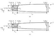
各単位発光部2は、搭載面5、発光部本体6、第1の筒状反射部7、および第2の筒状反射部8から主として構成される。なお、以下では、第1の筒状反射部7の搭載面5側の端部の断面を断面P1、第1の筒状反射部7と第2の筒状反射部8との接続部分における断面を断面P2、第2の筒状反射部8の光出射側の端部の断面を断面P3とする。また、断面P1におけるx軸方向の大きさをx1、y軸方向の大きさをy1、断面積をS1、断面P2におけるx軸方向の大きさをx2、y軸方向の大きさをy2、断面積をS2、断面P3におけるx軸方向の大きさをx3、y軸方向の大きさをy3、断面積をS3とする(図5等参照)。また、第1の筒状反射部7のz軸方向の長さをL1x(x軸方向部分)、L1y(y軸方向部分)、第2の筒状反射部8のz軸方向の長さをL2x(x軸方向部分)、L2y(y軸方向部分)とする(図5等参照)。Each unit
搭載面5は、モジュール基板3の表面を利用して設けられ、各単位発光部2の配列に対応して所定の配列となるように複数設けられる。発光部本体6は、搭載面5上に設けられ、搭載面5上に搭載されるLED素子9と、このLED素子9の少なくとも主光出射側の表面を被覆する蛍光体層11とから構成される。 The mounting
第1の筒状反射部7および第2の筒状反射部8は、例えば、反射板4を利用して設けられ、厚さ方向に貫通する貫通孔からなる。第1の筒状反射部7および第2の筒状反射部8は、各単位発光部2の配列に対応して所定の配列となるように複数設けられる。第1の筒状反射部7は、発光部本体6の側面を囲むものであり、搭載面5から少なくとも発光部本体6の光出射側の表面(蛍光体層11の光出射側の表面)の位置まで設けられる。このように第1の筒状反射部7の内部に発光部本体6を設けることで、初期の発光面積を効果的に低減できる。 The 1st
第2の筒状反射部8は、第1の筒状反射部7の光出射側に接続され、第1の筒状反射部側の断面P2の断面積S2に対して光出射側となる断面P3の断面積S3が大きくなる。第1の筒状反射部7の光出射側にこのような第2の筒状反射部8を接続することで、LEDモジュール1全体の大きさや厚さの増加を抑制しつつ、指向角を低減できる。Second cylindrical
図3は、LEDモジュール1の変形例を示す断面図である。
このLEDモジュール1は、モジュール基板3に凹部を設け、この凹部の底面を搭載面5、側面を第1の筒状反射部7とし、反射板4には第2の筒状反射部8のみを設けたものである。このように、第1の筒状反射部7と第2の筒状反射部8とは必ずしも反射板4に一体に設ける必要はなく、モジュール基板3と反射板4とに分けて設けてもよい。モジュール基板3に凹部を設けて搭載面5や第1の筒状反射部7とすることで、第1の筒状反射部7内への単位発光部2の形成が容易になり、また反射板4には第2の筒状反射部8のみを設ければよいことから、反射板4の形成も容易となる。FIG. 3 is a cross-sectional view showing a modification of the
In this
以下、単位発光部2について詳細に説明する。 Hereinafter, the unit
図4は、単位発光部2の一例を示す斜視図である。
LED素子9の平面形状は、通常、正方形状や矩形状等の四角形状とされる。第1の筒状反射部7のxy断面における断面形状は、例えば、LED素子9の平面形状と相似形状の正方形状や矩形状等の四角形状とされ、z軸方向に一定とされる。第1の筒状反射部7の断面形状をLED素子9の平面形状と相似形状とすることで、LED素子9と第1の筒状反射部7との間における大きな隙間を少なくして光利用効率を向上でき、また、発光面積を極力小さくすることで光の放射角を狭めることになる。また、第1の筒状反射部7に接続される第2の筒状反射部8についても、例えば、第1の筒状反射部7の断面形状に合わせて、正方形状や矩形状等の四角形状とされる。FIG. 4 is a perspective view illustrating an example of the unit
The planar shape of the
図5は、単位発光部2の一例を示す断面図であり、図5(a)は中心軸axを含むxz断面における断面図、図5(b)は中心軸axを含むyz断面における断面図である。LED素子9の大きさは、必ずしも限定されないが、x軸方向の大きさx0は0.2〜1mm、y軸方向の大きさy0は0.2〜1mmが好ましい。5A and 5B are cross-sectional views showing an example of the unit light-emitting
第1の筒状反射部7の長さ(L1x、L1y)は、いずれも発光部本体6の光出射側の表面に達するものであればよく、通常、0.3〜1mmが好ましい。LED素子9の主光出射側の表面の面積S0に対する第1の筒状反射部7の断面P2の断面積S2の面積比(S2/S0)は5以下が好ましい。面積比(S2/S0)を5以下とすることで、発光部本体6の発光面積を低減して指向角を低減できる。また、LED素子9と第1の筒状反射部7との間の隙間を少なくして発光効率を向上できる。The length of the first cylindrical reflective portion 7(L 1x, L1y) can be any any one reaching the surface of the light emitting side of the
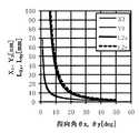
図6に、面積比(S2/S0)と単位発光部2の指向角(θx(x軸方向の指向角)、θy(y軸方向の指向角))との関係を示す。また、図7に、図6に示す面積比(S2/S0)におけるy軸方向の出射角度と光度との関係を示す。図6に示すように、面積比(S2/S0)を5以下とすることで、例えば、単位発光部2の指向角を20°以下にできる。面積比(S2/S0)は3以下がより好ましく、1であってもよい。FIG. 6 shows a relationship between the area ratio (S2 / S0 ) and the directivity angle (θx (directivity angle in the x-axis direction), θy (directivity angle in the y-axis direction)) of the unit
なお、図6、7における面積比(S2/S0)の調整は、LED素子9の面積S0を固定し、第1の筒状反射部7の断面P2の面積S2を変更することにより行った。単位発光部2の構成は以下に示す通りである。
LED素子9:x0=0.4mm、y0=0.5mm、厚さ=0.12mm
断面P1:x1=0.5〜1.1mm、y1=0.6〜1.2mm
断面P2:断面P1と同様
断面P3:x3=3.8〜6.1mm、y3=4.6〜6.4mm
長さL1x、L1y=0.6mm
長さL2x、L2y=19.7mmThe adjustment of the area ratio (S2 / S0 ) in FIGS. 6 and 7 fixes the area S0 of the
LED element 9: x0 = 0.4 mm, y0 = 0.5 mm, thickness = 0.12 mm
Cross section P1 : x1 = 0.5 to 1.1 mm, y1 = 0.6 to 1.2 mm
Section P2 : Similar to section P1 Section P3 : x3 = 3.8 to 6.1 mm, y3 = 4.6 to 6.4 mm
Length L1x , L1y = 0.6mm
Length L2x , L2y = 19.7 mm
また、上記結果から、LED素子9の大きさと第1の筒状反射部7の大きさとの差については、x軸方向の差x1−x0は0.5mm以下が好ましく、y軸方向の差y1−y0は0.5mm以下が好ましいことがわかる。x軸方向における差x1−x0は0.3mm以下がより好ましく、y軸方向における差y1−y0は0.3mm以下がより好ましい。Further, from the above results, the
第2の筒状反射部8は、例えば、CPC(compound parabolic concentrator=複合放物面集光器)が好ましい。CPCによれば、指向角の低減に加えて、そのレンズ機能により集光効率を向上でき、出射角度に対する光度を均一化できるとともに、集光のためのレンズ等の光学部品を省略して小型化できる。第2の筒状反射部8の光出射側における断面P3の大きさ(x3、y3)は、例えば、所望とするx軸方向、y軸方向の指向角(θx、θy)に応じて以下の範囲が好ましい。また、第2の筒状反射部8の長さ(L2x、L2y)についても、例えば、所望とするx軸方向、y軸方向の指向角(θx、θy)に応じて以下の範囲が好ましい。The second
x3≧x2/sin(θx/2)
y3≧y2/sin(θy/2)
L2x≧x2(1+sin(θx/2))/(2tan(θx/2)・sin(θx/2))
L2y≧y2(1+sin(θy/2))/(2tan(θy/2)・sin(θy/2))x3 ≧ x2 / sin (θx / 2)
y3 ≧ y2 / sin (θy / 2)
L2x ≧ x2 (1 + sin (θx / 2)) / (2 tan (θx / 2) · sin (θx / 2))
L2y ≧ y2 (1 + sin (θy / 2)) / (2 tan (θy / 2) · sin (θy / 2))
図8に、上記した指向角と大きさ(x3、y3)との関係、および指向角と長さ(L2x、L2y)との関係を示す。また、図9に、指向角と面積比(S3/S2)との関係を示す。図9に示されるように、例えば、指向角を30度以下にする場合、面積比(S3/S2)は15以上が好ましい。また、面積比(S3/S2)は、15以上であれば必ずしも制限されないが、通常、指向角15度に対応する59程度までが好ましく、これ以下とすることで第2の筒状反射部8の大きさ(x3、y3)を抑制できる。FIG. 8 shows the relationship between the directivity angle and the size (x3 , y3 ) and the relationship between the directivity angle and the length (L2x , L2y ). FIG. 9 shows the relationship between the directivity angle and the area ratio (S3 / S2 ). As shown in FIG. 9, for example, when the directivity angle is 30 degrees or less, the area ratio (S3 / S2 ) is preferably 15 or more. Further, the area ratio (S3 / S2 ) is not necessarily limited as long as it is 15 or more, but normally, it is preferably up to about 59 corresponding to the directivity angle of 15 degrees, and by setting it below this, the second cylindrical reflection is performed. The size (x3 , y3 ) of the
第2の筒状反射部8の光出射側における断面P3の大きさ(x3、y3)は、通常、x3=1.9〜3.8mm、y3=2.3〜4.6mmが好ましい。また、第2の筒状反射部8の長さ(L2x、L2y)は、通常、5〜20mmが好ましい。The size (x3 , y3 ) of the cross section P3 on the light exit side of the second
図10は、第2の筒状反射部8の壁部をCPCのような放物面を有するものから単なる平面に変更した変形例を示すものである。第2の筒状反射部8の壁部は、必ずしもCPCのような放物面に限られず、平面とした場合でもCPCの場合と同様に指向角を低減できる。以下、このような壁部が平面のものをテーパー状として説明する。テーパー状のものについても、第2の筒状反射部8の光出射側における断面P3の大きさ(x3、y3)、面積比(S3/S2)、長さ(L2x、L2y)等はCPCの場合と同様が好ましい。FIG. 10 shows a modification in which the wall portion of the second
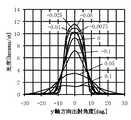
図11に、単位発光部2における出射角度(x軸方向、y軸方向)と、光度との関係を示す。図中、「cpc」は、第2の筒状反射部8をCPCとしたもの、「taper」は、第2の筒状反射部8をテーパー状としたもの、「−X]はx軸方向、「−Y]はy軸方向を示す。図11から明らかなように、CPC、テーパー状のいずれの場合にも指向角を十分に低減できることがわかる。なお。このときの指向角は、CPCの場合、θx=14°、θy=15°、テーパー状の場合、θx=14°、θy=15°となっている。また、テーパー状のものについては、中心部分の光度が高くなり、周辺部分の光度が低くなるが、CPCの場合には、出射角度に対して光度を均一にできることがわかる。FIG. 11 shows the relationship between the emission angle (x-axis direction and y-axis direction) and the luminous intensity in the unit
なお、単位発光部2の構成は以下に示す通りである。
LED素子9:x0=0.4mm、y0=0.5mm、厚さ=0.12mm
断面P1:x1=0.5mm、y1=0.6mm
断面P2:断面P1と同様
断面P3:x3=3.8mm、y3=4.6mm
長さL1x、L1y=0.6mm
長さL2x、L2y=19.7mmIn addition, the structure of the unit
LED element 9: x0 = 0.4 mm, y0 = 0.5 mm, thickness = 0.12 mm
Section P1 : x1 = 0.5 mm, y1 = 0.6 mm
Section P2 : Same as section P1 Section P3 : x3 = 3.8 mm, y3 = 4.6 mm
Length L1x , L1y = 0.6mm
Length L2x , L2y = 19.7 mm
第2の筒状反射部8の内部は、CPC、テーパー状のいずれについても、単なる空洞としてもよいが、蛍光体層11と第2の筒状反射部8の内部空間との界面反射による外部に取り出せない光量ロスを低減するために内部充填材を設けることが好ましい。内部充填材は、例えば、第2の筒状反射部8の全体に充填され、蛍光体層11に使用されるシリコーン樹脂等の透明樹脂の屈折率1.41(波長460nmの光における屈折率。以下、同様)に近い屈折率を有するものが好ましい。内部充填材としては、例えば、シリコーン樹脂、エポキシ樹脂、アクリル樹脂等が挙げられる。垂直入射時のフレネル反射は次の式で与えられる。 The inside of the second
反射率={(n1−n2)/(n1+n2)}2×100[%]
n1:蛍光体層11(シリコーン樹脂)の屈折率1.41
n2:内部充填材の屈折率
上記式から、反射率を0.5%以下とするためには、内部充填材の屈折率n2は1.22〜1.63が好ましい。Reflectivity = {(n1 −n2 ) / (n1 + n2 )}2 × 100 [%]
n1 : Refractive index of phosphor layer 11 (silicone resin) 1.41
n2 : Refractive index of internal filler From the above formula, in order to make the reflectance 0.5% or less, the refractive index n2 of the internal filler is preferably 1.22 to 1.63.
内部充填材を設ける場合、その光出射側となる断面P3には光利用効率を向上させるための充填材用反射防止層を設けることが好ましい。充填材用反射防止層として単層の反射防止層を設ける場合、垂直入射時に反射率が0となる条件は以下となる。When providing the internal filler, it is preferable to provide a filler for anti-reflective layer for improving light use efficiency in the sectional P3 serving as the light emitting side. When a single-layer antireflection layer is provided as the antireflection layer for filler, the conditions under which the reflectivity is 0 when perpendicularly incident are as follows.
n3=n21/2
d3=λ/(4×n3)
n2:内部充填材の屈折率(例えば、シリコーン樹脂の屈折率1.41)
n3:充填材用反射防止層の屈折率
d3:充填材用反射防止層の厚み
λ :波長
上記条件式から、光学膜厚を0.2〜0.3λとする場合、反射率を1%以下とするには、充填材用反射防止層の屈折率n3は1.09〜1.30が好ましい。n3 = n21/2
d3 = λ / (4 × n3 )
n2 : Refractive index of internal filler (for example, refractive index of silicone resin 1.41)
n3 : Refractive index of antireflection layer for filler d3 : Thickness of antireflection layer for filler λ: Wavelength From the above conditional expression, when the optical film thickness is 0.2 to 0.3λ, the reflectance is 1 percent or less, the refractive indexn 3 of the filler for the antireflection layer is preferably 1.09 to 1.30.
また、特に第2の筒状反射部8がテーパー状の場合、CPCの場合と比べて、壁部が平面なことから加工性に優れるが、上記したように出射角度に対する光度が均一となりにくい。このため、例えば、図12に示すように、出射角度に対する光度を均一にするためのレンズ部12を設けることが好ましい。レンズ部12は、例えば、複数のレンズ部12が一体に形成され、配列されてなるレンズ板の一部とすることができる。 In particular, when the second
レンズ部12は、第2の筒状反射部8の光出射側の端部P3を覆うように設けられ、光出射側に凸状となるものであり、球面状であってもよいし、非球面状であってもよい。レンズ形状は、例えば、以下の自由曲面レンズの式で表記できるが、実質的にレンズ形状が同じであれば表記方法は限定されない。

k:円錐定数
Ai:多項式係数
Ei:多項式(x,y,x2,xy,y2・・・・)
1項目は2次曲面を表し、2項目は多項式を表している。
今回は、c=0とし、2項目のi=3,5項であるx2とy2でレンズ曲面を記述する。
よって、上記式は以下のように記述される。
Z=A3x2+A5y2One item represents a quadric surface and two items represent a polynomial.
This time, c = 0, and the lens curved surface is described by x2 and y2 which are two items i = 3 and 5.
Therefore, the above formula is described as follows.
Z = A3 x2 + A5 y2
図13に、多項式係数A3を変更したときのx軸方向の出射角度と光度との関係を、図14に、多項式係数A5を変更したときのy軸方向の出射角度と光度との関係をそれぞれ示す。図13、14から明らかなように、多項式係数A3、A5については、例えば、−0.05〜0が好ましいことがわかる。ここで「−」の記号は、レンズが凸レンズであることを意味する。−0.05より小さいとレンズ厚みが厚くなる傾向にあるため薄型化の点で不利となる。また、0より大きいと指向角が広がる傾向にあり、スポット光用途に適さない。レンズ部12の厚さは、レンズ形状を表す多項式係数から、例えば、0.5mm以下が好ましい。このような多項式係数、厚さとすることで、出射角度に対する光度の均一性を調整できる。13, the relationship between the x-axis direction of the emission angle and intensity when changing the polynomial coefficients A3, in Fig. 14, the relationship between the y-axis direction of the emission angle and intensity when changing the polynomial coefficients A5 Respectively. As is apparent from FIGS. 13 and 14, for the polynomial coefficients A3 and A5 , for example, −0.05 to 0 is preferable. Here, the symbol “−” means that the lens is a convex lens. If it is smaller than -0.05, the lens thickness tends to increase, which is disadvantageous in terms of thinning. On the other hand, if it is larger than 0, the directivity angle tends to widen, which is not suitable for spot light applications. The thickness of the
なお、単位発光部2のレンズ部12以外の構成は以下に示す通りである。
LED素子9:x0=0.4mm、y0=0.5mm、厚さ=0.12mm
断面P1:x1=0.5mm、y1=0.6mm
断面P2:断面P1と同様
断面P3:x3=3.8mm、y3=4.6mm
長さL1x、L1y=0.6mm
長さL2x、L2y=19.7mmThe configuration of the unit
LED element 9: x0 = 0.4 mm, y0 = 0.5 mm, thickness = 0.12 mm
Section P1 : x1 = 0.5 mm, y1 = 0.6 mm
Section P2 : Same as section P1 Section P3 : x3 = 3.8 mm, y3 = 4.6 mm
Length L1x , L1y = 0.6mm
Length L2x , L2y = 19.7 mm
レンズ部12の出射側の表面には、光利用効率を向上させるためのレンズ用反射防止層を設けることが好ましい。レンズ用反射防止層として単層の反射防止層を設ける場合、垂直入射時に反射率が0となる条件は以下となる。
n5=n41/2
d4=λ/(4×n4)
n4:レンズ部12の屈折率(例えばB270の屈折率1.52)
n5:レンズ用反射防止層の屈折率
d5:レンズ用反射防止層の厚み
λ :波長
上記条件式から、光学膜厚を0.2〜0.3λとする場合、反射率を1%以下とするには、レンズ用反射防止層の屈折率n5は1.14〜1.33が好ましい。It is preferable to provide a lens antireflection layer for improving the light utilization efficiency on the surface on the exit side of the
n5 = n41/2
d4 = λ / (4 × n4 )
n4 : the refractive index of the lens unit 12 (for example, the refractive index of B270 is 1.52)
n5 : Refractive index of the antireflection layer for lens d5 : Thickness of the antireflection layer for lens λ: Wavelength From the above conditional expression, when the optical film thickness is 0.2 to 0.3λ, the reflectance is 1% or less. and to have a refractive indexn 5 of the lens anti-reflective layer is preferably from 1.14 to 1.33.
表1に、単位発光部2における光利用効率の比較結果を示す。なお、結果は入射光束1ルーメンあたりの出射光束の割合で示した。ここで、構成1は、第2の筒状反射部8をCPCとしたもの、構成2は、第2の筒状反射部8をテーパー状とし、かつレンズ部12を設けたものである。 Table 1 shows a comparison result of the light use efficiency in the unit
また、施策[1]は、第1の筒状反射部7および第2の筒状反射部8の反射率を向上させるものであり、構成材料をアルミニウムに変えてLTCC(0.5mm厚み、反射率98.5%)とするものである。施策[2]は、第2の筒状反射部8に屈折率1.41のシリコーン樹脂からなる内部充填材を充填するものである。施策[3]は、構成1の場合、内部充填材を設ける際にその光出射側の断面P3に中空シリカ微粒子を含有する充填材用反射防止層(屈折率1.19)を設け、構成2の場合、レンズ部12の光出射側の表面に中空シリカ微粒子を含有するレンズ用反射防止層(屈折率1.23)を設けるものである。なお、構成1、2の施策を施していないときの基本構成は、以下の通りである。The measure [1] is to improve the reflectivity of the first
[構成1]
LED素子9:x0=0.4mm、y0=0.5mm、厚さ=0.12mm
断面P1:x1=0.5mm、y1=0.6mm
断面P2:断面P1と同様
断面P3:x3=3.8mm、y3=4.6mm
長さL1x、L1y=0.6mm
長さL2x、L2y=19.7mm
第1の筒状反射部7、第2の筒状反射部8の構成材料:アルミニウム(反射率92%)
第2の筒状反射部8:CPC
レンズ部12:なし[Configuration 1]
LED element 9: x0 = 0.4 mm, y0 = 0.5 mm, thickness = 0.12 mm
Section P1 : x1 = 0.5 mm, y1 = 0.6 mm
Section P2 : Same as section P1 Section P3 : x3 = 3.8 mm, y3 = 4.6 mm
Length L1x , L1y = 0.6mm
Length L2x , L2y = 19.7 mm
Constituent material of the first
Second cylindrical reflector 8: CPC
Lens part 12: None
[構成2]
LED素子9:x0=0.4mm、y0=0.5mm、厚さ=0.12mm
断面P1:x1=0.5mm、y1=0.6mm
断面P2:断面P1と同様
断面P3:x3=3.8mm、y3=4.6mm
長さL1x、L1y=0.6mm
長さL2x、L2y=19.7mm
第1の筒状反射部7、第2の筒状反射部8の構成材料:アルミニウム(反射率92%)
第2の筒状反射部8:テーパー状
レンズ部12:あり(レンズ形状:Z=−0.025x2−0.025y2)[Configuration 2]
LED element 9: x0 = 0.4 mm, y0 = 0.5 mm, thickness = 0.12 mm
Section P1 : x1 = 0.5 mm, y1 = 0.6 mm
Section P2 : Same as section P1 Section P3 : x3 = 3.8 mm, y3 = 4.6 mm
Length L1x , L1y = 0.6mm
Length L2x , L2y = 19.7 mm
Constituent material of the first
Second cylindrical reflecting portion 8: tapered lens portion 12: present (lens shape: Z = −0.025x2 −0.025y2 )
表1から明らかなように、施策[1]〜[3]を行うことで光利用効率を向上できることがわかる。構成1の場合、施策[1]が光利用効率を向上させるために効果的であり、施策[1]〜[3]の全てを行うことで光利用効率を大幅に向上できることがわかる。一方、構成2の場合、施策[2]が光利用効率を向上させるために効果的であり、施策[1]〜[3]の全てを行うことで光利用効率を大幅に向上できることがわかる。 As is clear from Table 1, it can be seen that the light utilization efficiency can be improved by implementing the measures [1] to [3]. In the case of the
LEDモジュール1の厚さ、すなわちモジュール基板3から反射板4またはレンズ部12までの全体の厚さは21mm以下が好ましい。このような厚さとすることで、小型のLEDランプ、例えば、最大径部分が50〜70mm程度のものに好適となる。LEDモジュール1の厚さは、21mm以下であれば特に限定されないが、通常、厚さを抑制しつつスポット光の指向角である20〜30度にも対応できる7〜13mmが好ましい。なお、LEDモジュール1のx軸方向、y軸方向の大きさ(xm、ym)は、通常、xm=10〜49mm、ym=10〜49mmが好ましい。The thickness of the
また、単位発光部2の指向角は30度以下が好ましい。なお、単位発光部2の平面形状や断面形状が矩形状等であるためにx軸方向とy軸方向とで指向角が異なる場合、ここでの指向角は両方向の指向角が30度以下となることを意味する。単位発光部2の指向角は30度以下であれば必ずしも限定されないが、指向角を小さくするためには第2の筒状反射部8の長さ(L2x、L2y)を長くする必要があり、結果として単位発光部2の全体の厚さが増加することから、通常、15〜30度が好ましい。The directivity angle of the unit
LED素子9としては、青色光を発する青色LED素子が挙げられる。また、蛍光体層11としては、シリコーン樹脂等の透明樹脂中に、青色光により励起されて黄色光を発する黄色蛍光体が分散されたものが挙げられる。 Examples of the
モジュール基板3は、例えば、LED素子9が直接実装されるチップオンボード型の基板である。モジュール基板3としては、例えば、樹脂で構成される電気絶縁基板と配線パターンから形成されたものや、熱伝導性の良好な金属材料、具体的にはアルミニウム等からなる基板本体上に、シリコーン樹脂等からなる電気絶縁層を介して配線パターンが形成されたものが挙げられる。 The
また、モジュール基板3としては、公知のセラミックス基板、例えば窒化珪素基板、窒化アルミニウム基板等が挙げられる。さらに、モジュール基板3としては、ガラス粉末とセラミックス粉末とを含むガラスセラミックス組成物を焼成したガラスセラミックス基板、いわゆる低温同時焼成基板(LTCC基板)が挙げられる。モジュール基板3としては、熱伝導性、反射特性、製造性等が良好であることから、ガラスセラミックス基板が好適に用いられる。 The
以下、ガラスセラミックス基板について具体的に説明する。
ガラスセラミックス基板は、ガラス粉末とセラミックス粉末とを含むガラスセラミックス組成物の焼成物であり、例えば、ガラスセラミックス組成物を含有するスラリーをシート状に成形してグリーンシートとし、このグリーンシートを焼成して製造される。Hereinafter, the glass ceramic substrate will be specifically described.
The glass ceramic substrate is a fired product of a glass ceramic composition containing glass powder and ceramic powder. For example, a slurry containing the glass ceramic composition is formed into a sheet to form a green sheet, and the green sheet is fired. Manufactured.
ガラス粉末としては、例えば、酸化物基準のモル%表示で、SiO2を57〜65%、B2O3を13〜18%、CaOを9〜23%、Al2O3を3〜8%、K2OおよびNa2Oから選ばれる少なくとも一方を合計で0.5〜6%含有するものが挙げられる。As the glass powder, for example, by mol% based on oxides, theSiO 2 57~65%, B 2 O 3 of 13-18%, 9-23% of CaO, theAl 2O 3 3 to 8% , K2 O and Na2 O are included and the total content is 0.5 to 6%.
SiO2は、ガラスのネットワークフォーマとなるものである。SiO2の含有量を57%以上とすることで、ガラスを安定化させ、また化学的耐久性を確保できる。一方、SiO2の含有量を65%以下とすることで、ガラス溶融温度やTgで表わされるガラス転移点の過度な上昇を抑制できる。SiO2の含有量は、好ましくは58%以上、より好ましくは59%以上、特に好ましくは60%以上である。また、SiO2の含有量は、好ましくは64%以下、より好ましくは63%以下である。本明細書では以下ガラス転移点をTgという。SiO2 is a glass network former. By setting the content of SiO2 to 57% or more, glass can be stabilized and chemical durability can be secured. On the other hand, by setting the content of SiO2 to 65% or less, an excessive increase in the glass transition point represented by the glass melting temperature or Tg can be suppressed. The content of SiO2 is preferably 58% or more, more preferably 59% or more, and particularly preferably 60% or more. Further, the content of SiO2 is preferably 64% or less, more preferably 63% or less. In the present specification, the glass transition point is hereinafter referred to as Tg.
B2O3は、ガラスのネットワークフォーマとなる。B2O3の含有量を13%以上とすることで、ガラス溶融温度やTgの過度な上昇を抑制できる。一方、B2O3の含有量を18%以下とすることで、ガラスを安定化させ、また化学的耐久性を確保できる。B2O3の含有量は、好ましくは14%以上、より好ましくは15%以上である。また、B2O3の含有量は、好ましくは17%以下、より好ましくは16%以下である。B2 O3 is a glass network former. By setting the content of B2 O3 to 13% or more, an excessive increase in the glass melting temperature or Tg can be suppressed. On the other hand, by setting the content of B2 O3 to 18% or less, the glass can be stabilized and chemical durability can be secured. The content of B2 O3 is preferably 14% or more, more preferably 15% or more. Further, the content of B2 O3 is preferably 17% or less, more preferably 16% or less.
Al2O3は、ガラスの安定性、化学的耐久性、および強度を向上させる。Al2O3の含有量を3%以上とすることで、ガラスを安定化させることができる。一方、Al2O3の含有量を8%以下とすることで、ガラス溶融温度やTgの過度な上昇を抑制できる。Al2O3の含有量は、好ましくは4%以上、より好ましくは5%以上である。また、Al2O3の含有量は、好ましくは7%以下、より好ましくは6%以下である。Al2 O3 improves the stability, chemical durability, and strength of the glass. By setting the content of Al2 O3 to 3% or more, the glass can be stabilized. On the other hand, by setting the content of Al2 O3 to 8% or less, an excessive increase in the glass melting temperature and Tg can be suppressed. The content of Al2 O3 is preferably 4% or more, more preferably 5% or more. Further, the content of Al2 O3 is preferably 7% or less, more preferably 6% or less.
CaOは、ガラスの安定性や結晶の析出性を高めるとともに、ガラス溶融温度やTgを低下させる。CaOの含有量を9%以上とすることで、ガラス溶融温度の過度な上昇を抑制できる。一方、CaOの含有量を23%以下とすることで、ガラスを安定化させることができる。CaOの含有量は、好ましくは12%以上、より好ましくは13%以上、特に好ましくは14%以上である。また、CaOの含有量は、好ましくは22%以下、より好ましくは21%以下、特に好ましくは20%以下である。 CaO increases glass stability and crystal precipitation, and lowers the glass melting temperature and Tg. By making the content of
K2O、Na2Oは、Tgを低下させる。K2OおよびNa2Oの合計した含有量を0.5%以上とすることで、ガラス溶融温度やTgの過度な上昇を抑制できる。一方、K2OおよびNa2Oの合計した含有量を6%以下とすることで、化学的耐久性、特に耐酸性を確保できるとともに、電気的絶縁性も確保できる。K2OおよびNa2Oの合計した含有量は、0.8%以上5%以下が好ましい。K2 O and Na2 O lower Tg. By making the total content of K2 O and Na2 O 0.5% or more, an excessive increase in the glass melting temperature or Tg can be suppressed. On the other hand, when the total content of K2 O and Na2 O is 6% or less, chemical durability, particularly acid resistance can be secured, and electrical insulation can be secured. The total content of K2 O and Na2 O is preferably 0.8% or more and 5% or less.
ガラス粉末は、必ずしも上記成分のみからなるものに限定されず、Tg等の諸特性を満たす範囲で他の成分を含有することができる。他の成分を含有する場合、その合計した含有量は10%以下が好ましい。 Glass powder is not necessarily limited to what consists only of the said component, but can contain another component in the range with which various characteristics, such as Tg, are satisfy | filled. When other components are contained, the total content is preferably 10% or less.
ガラス粉末は、Tgが550〜700℃のものが好ましい。Tgを550℃以上とすることで、グリーンシートの脱脂が容易となる。また、700℃以下とすることで、収縮開始温度を低下させ、寸法精度を向上させることができる。 The glass powder preferably has a Tg of 550 to 700 ° C. By making Tg 550 ° C. or higher, the green sheet can be easily degreased. Moreover, shrinkage start temperature can be lowered | hung by setting it as 700 degrees C or less, and a dimensional accuracy can be improved.
また、ガラス粉末は、800〜930℃で焼成したときに結晶が析出することが好ましい。結晶が析出することで、十分な機械的強度を得ることができる。さらに、DTA(示差熱分析)により測定されるTcで表記される結晶化ピーク温度は880℃以下が好ましい。Tcを880℃以下とすることで、寸法精度が向上する。 Moreover, it is preferable that a crystal | crystallization precipitates when glass powder is baked at 800-930 degreeC. A sufficient mechanical strength can be obtained by the precipitation of crystals. Furthermore, the crystallization peak temperature represented by Tc measured by DTA (differential thermal analysis) is preferably 880 ° C. or less. By setting Tc to 880 ° C. or less, the dimensional accuracy is improved.
ガラス粉末の調製は、同様の組成を有するガラスを溶融法によって製造し、例えば、乾式粉砕法や湿式粉砕法によって粉砕することにより行う。湿式粉砕法の場合、溶媒として水またはエチルアルコールを用いることが好ましい。粉砕機としては、例えばロールミル、ボールミル、ジェットミル等が挙げられる。 The glass powder is prepared by producing a glass having the same composition by a melting method, for example, by pulverizing by a dry pulverization method or a wet pulverization method. In the case of the wet pulverization method, it is preferable to use water or ethyl alcohol as a solvent. Examples of the pulverizer include a roll mill, a ball mill, and a jet mill.
ガラス粉末の50%粒径(D50)は0.5〜2μmが好ましい。ガラス粉末のD50を0.5μm以上とすることで、ガラス粉末の凝集が抑制されて取り扱い性が向上するとともに、均一分散が容易となる。一方、ガラス粉末のD50を2μm以下とすることで、ガラス軟化温度の上昇や焼結不足を抑制できる。粒径の調整は、例えば、粉砕後に必要に応じて分級することにより行う。The 50% particle size (D50 ) of the glass powder is preferably 0.5 to 2 μm. The D50 of the glass powder by the above 0.5 [mu] m, aggregation of the glass powder is suppressed thereby improving the handling properties, uniform dispersion becomes easy. On the other hand, by the D50 of the glass powder and 2μm or less, it can be suppressed from increasing and insufficient sintering of the glass softening temperature. The particle size is adjusted by, for example, classification as necessary after pulverization.
セラミックス粉末は、モジュール基板3の反射率を向上させる。セラミックス粉末としては、従来からLTCC基板の製造に用いられるセラミックス粉末が挙げられ、例えば、アルミナ粉末、ジルコニア粉末、安定化ジルコニア粉末、チタニア粉末、これらから選ばれる2種以上の混合物が挙げられる。特に、アルミナ粉末とともに、アルミナ粉末よりも高い屈折率を有するセラミックス粉末を用いることが好ましい。このようなものとすることで、強度や反射率の高いモジュール基板3を得ることができる。例えば、アルミナの屈折率は1.8程度、ジルコニアの屈折率は2.2程度、チタニアの屈折率は2.7程度であり、ジルコニア粉末等はアルミナ粉末に比べて高い屈折率を有している。セラミックス粉末の50%粒径(D50)は、0.5〜4μmが好ましい。The ceramic powder improves the reflectance of the
ガラス粉末とセラミックス粉末とは、例えばガラス粉末が30〜50質量%、セラミックス粉末が70〜50質量%となるように配合し、混合して、ガラスセラミックス組成物とする。このガラスセラミックス組成物に、バインダー、必要に応じて可塑剤、分散剤、溶剤等を添加することによりスラリーを調製する。 The glass powder and the ceramic powder are, for example, blended so that the glass powder is 30 to 50% by mass and the ceramic powder is 70 to 50% by mass and mixed to obtain a glass ceramic composition. A slurry is prepared by adding a binder and, if necessary, a plasticizer, a dispersant, a solvent, and the like to the glass ceramic composition.
バインダーとしては、例えば、ポリビニルブチラール、アクリル樹脂等が挙げられる。可塑剤としては、例えば、フタル酸ジブチル、フタル酸ジオクチル、フタル酸ブチルベンジル等を使用できる。溶剤としては、例えば、トルエン、キシレン、2−プロパノール、2−ブタノール等の有機溶剤が挙げられる。 Examples of the binder include polyvinyl butyral and acrylic resin. As the plasticizer, for example, dibutyl phthalate, dioctyl phthalate, butyl benzyl phthalate and the like can be used. Examples of the solvent include organic solvents such as toluene, xylene, 2-propanol and 2-butanol.
スラリーは、例えば、ドクターブレード法によってシート状に成形し、乾燥させて、グリーンシートとする。グリーンシートは、1枚のみを用いてもよいし、2枚以上を重ね合わせて熱圧着してもよい。グリーンシートには、必要に応じて導体ペーストの塗布または充填を行い、焼成により、配線、電極、層間ビア等となるものを形成する。導体ペーストの塗布、充填は、スクリーン印刷、メタルマスク印刷により行うことができる。導体ペーストとしては、例えば、銅、銀、金等を主成分とする金属粉末に、エチルセルロース等のビヒクル、必要に応じて溶剤等を添加してペースト状としたものを使用できる。なお、上記金属粉末としては、銀粉末、銀と白金またはパラジウムからなる金属粉末が好ましく用いられる。 The slurry is formed into a sheet shape by, for example, a doctor blade method and dried to obtain a green sheet. Only one green sheet may be used, or two or more green sheets may be superposed and thermocompression bonded. The green sheet is coated or filled with a conductive paste as necessary, and is baked to form wiring, electrodes, interlayer vias, or the like. The application and filling of the conductive paste can be performed by screen printing or metal mask printing. As the conductive paste, for example, a paste obtained by adding a vehicle such as ethyl cellulose to a metal powder containing copper, silver, gold or the like as a main component and, if necessary, a solvent or the like can be used. In addition, as said metal powder, the metal powder which consists of silver powder and silver, platinum, or palladium is used preferably.
導体ペーストの塗布等が行われたグリーンシートは、必要に応じてバインダーを除去する脱脂を行った後、焼成を行ってモジュール基板3とする。脱脂は、例えば500〜600℃で1〜10時間保持する条件で行う。脱脂温度を500℃以上、脱脂時間を1時間以上とすることで、バインダーを十分に除去できる。一方、脱脂温度は600℃程度、脱脂時間は10時間程度もあればバインダー等を十分に除去でき、これ以下とすることで生産性を確保できる。 The green sheet on which the conductive paste is applied is degreased to remove the binder as necessary, and then fired to form the
焼成条件は、モジュール基板3における緻密な構造の獲得と生産性とを考慮して、800〜930℃の温度範囲で適宜時間を調整できる。焼成条件は、850〜900℃で20〜60分が好ましく、特に860〜880℃で20〜60分が好ましい。焼成温度を800℃以上とすることで、緻密な構造が得られる。一方、焼成温度を930℃以下とすることで、モジュール基板3の変形を抑制し、生産性も確保できる。なお、導体ペーストが銀を主成分とする金属粉末を含有する場合、焼成温度が880℃を超えると過度の軟化により所定の形状を維持できないおそれがある。 The firing conditions can be adjusted as appropriate in the temperature range of 800 to 930 ° C. in consideration of obtaining a dense structure and productivity in the
モジュール基板3には、必要に応じて、基板表面に露出する配線、電極等の表面導体を保護するための保護膜を設けることができる。保護膜としては、この種のモジュール基板に一般的なNi/Auメッキ等からなる導電性保護膜が挙げられる。 The
モジュール基板3の厚さは、通常、0.3〜2mmが好ましい。モジュール基板3の厚さを0.3mm以上とすることで、製造時の取り扱い性、機械的強度等を確保できる。モジュール基板3の厚さは、2mmあれば、製造時の取り扱い性、機械的強度等を十分に確保でき、これ以下とすることで、LEDモジュール1の全体の厚さを抑制できるとともに放熱特性も良好にできる。これにより、LEDランプに用いたときの大型化を抑制できる。 In general, the thickness of the
反射板4の構成材料は、金属材料、例えば、アルミニウム等としてもよいし、セラミックス、例えば、窒化珪素、窒化アルミニウム等としてもよいし、ガラスセラミックス、すなわちガラス粉末とセラミックス粉末とを含むガラスセラミックス組成物の焼成物としてもよい。ガラスセラミックス組成物としては、既に説明した組成を有するものが好適なものとして挙げられる。さらに、反射板4の構成材料は、無機材料に限られず、有機材料であってもよい。有機材料としては、例えば、電離放射線硬化性樹脂、熱硬化性樹脂、熱可塑性樹脂が挙げられる。 The constituent material of the reflecting
電離放射線硬化性樹脂は、電磁波または荷電粒子線、例えば紫外線または電子線等を照射することにより、架橋または重合反応にて硬化する樹脂である。このような電離放射線硬化性樹脂としては、例えば電離放射線重合性プレポリマーおよび/または電離放射線重合性モノマーを挙げることができる。 The ionizing radiation curable resin is a resin that is cured by crosslinking or polymerization reaction by irradiation with electromagnetic waves or charged particle beams such as ultraviolet rays or electron beams. Examples of such ionizing radiation curable resins include ionizing radiation polymerizable prepolymers and / or ionizing radiation polymerizable monomers.
電離放射線重合性プレポリマー(オリゴマーも包含する)としては、例えばポリエステル(メタ)アクリレート系、エポキシ(メタ)アクリレート系、ウレタン(メタ)アクリレート系、ポリオール(メタ)アクリレート系、シリコン(メタ)アクリレート、不飽和ポリエステル系等の分子中にラジカル重合性官能基を有する重合性オリゴマー、あるいはノボラック系型エポキシ樹脂プレポリマー、芳香族ビニルエーテル系樹脂プレポリマー等のエポキシ系樹脂等の分子中にカチオン重合性官能基を有する重合性オリゴマー等が挙げられる。なお、ここで、「(メタ)アクリレート」とは「アクリレートまたはメタクリレート」を意味する。 Examples of ionizing radiation polymerizable prepolymers (including oligomers) include polyester (meth) acrylates, epoxy (meth) acrylates, urethane (meth) acrylates, polyol (meth) acrylates, silicon (meth) acrylates, Cationically polymerizable functional groups in molecules such as unsaturated polyester-based polymerizable oligomers having radically polymerizable functional groups in the molecule, or novolak-type epoxy resin prepolymers, aromatic vinyl ether-based resin prepolymers, etc. Examples thereof include a polymerizable oligomer having a group. Here, “(meth) acrylate” means “acrylate or methacrylate”.
また、電離放射線重合性モノマー(単量体)としては、分子中にラジカル重合性官能基を有する重合性モノマーである多官能性(メタ)アクリレートが好ましく、具体的にはエチレングリコールジ(メタ)アクリレート、プロピレングリコールジ(メタ)アクリレート、トリメチロールプロパントリ(メタ)アクリレート、ジペンタエリスリトールペンタ(メタ)アクリレート、ジペンタエリスリトールヘキサ(メタ)アクリレート、カプロラクトン変性ジペンタエリスリトールヘキサ(メタ)アクリレート等が挙げられる。カチオン重合性官能基を有するモノマーとして、例えば、3,4−エポキシシクロへキセニルメチル−3',4'−エポキシシクロへキセンカルボキシレート等の脂環式エポキシド類、ビスフェノールAジグリシジルエーテル等グリシジルエーテル類、4−ヒドロキシブチルビニルエーテル等ビニルエーテル類、3−エチル−3−ヒドロキシメチルオキセタン等オキセタン類等が挙げられる。 The ionizing radiation polymerizable monomer (monomer) is preferably a polyfunctional (meth) acrylate which is a polymerizable monomer having a radical polymerizable functional group in the molecule, specifically ethylene glycol di (meth). Acrylate, propylene glycol di (meth) acrylate, trimethylolpropane tri (meth) acrylate, dipentaerythritol penta (meth) acrylate, dipentaerythritol hexa (meth) acrylate, caprolactone modified dipentaerythritol hexa (meth) acrylate, etc. It is done. Examples of the monomer having a cationic polymerizable functional group include alicyclic epoxides such as 3,4-epoxycyclohexenylmethyl-3 ′, 4′-epoxycyclohexenecarboxylate, and glycidyl ethers such as bisphenol A diglycidyl ether. , Vinyl ethers such as 4-hydroxybutyl vinyl ether, and oxetanes such as 3-ethyl-3-hydroxymethyloxetane.
熱硬化性樹脂としては、フェノール樹脂、フェノール−ホルマリン樹脂、尿素樹脂、尿素−ホルマリン樹脂、メラミン樹脂、ポリエステル−メラミン樹脂、メラミン−ホルマリン樹脂、アルキッド樹脂、エポキシ樹脂、エポキシ−メラミン樹脂、不飽和ポリエステル樹脂、ポリイミド樹脂、アクリル樹脂、ポリシロキサン樹脂、ポリウレタン樹脂、汎用の2液硬化型アクリル樹脂(アクリルポリオール硬化物)等が挙げられる。 Thermosetting resins include phenolic resin, phenol-formalin resin, urea resin, urea-formalin resin, melamine resin, polyester-melamine resin, melamine-formalin resin, alkyd resin, epoxy resin, epoxy-melamine resin, unsaturated polyester. Examples thereof include resins, polyimide resins, acrylic resins, polysiloxane resins, polyurethane resins, and general-purpose two-component curable acrylic resins (acrylic polyol cured products).
熱可塑性樹脂としては、ポリエチレンテレフタレート(PET)、ポリエチレンナフタレート(PEN)、エチレングリコール−テレフタル酸−イソフタル酸共重合体、テレフタル酸−エチレングリコール−1,4シクロヘキサンジメタノール共重合体、ポリエステル系熱可塑性エラストマー等のポリエステル樹脂、ポリエチレン、ポリプロピレン、環状ポリオレフィン、ポリメチルペンテン等のポリオレフィン樹脂、ポリ塩化ビニル、ポリ塩化ビニリデン等の含ハロゲン樹脂、ポリスチレン、アクリロニトリル−スチレン共重合体等のスチレン系樹脂、トリアセチルセルロース、ジアセチルセルロース、アセテートブチレートセルロース等のセルロース樹脂、熱可塑性ポリウレタン系樹脂、ポリカーボネート樹脂、ポリアミド樹脂等が挙げられる。 Examples of the thermoplastic resin include polyethylene terephthalate (PET), polyethylene naphthalate (PEN), ethylene glycol-terephthalic acid-isophthalic acid copolymer, terephthalic acid-ethylene glycol-1,4 cyclohexanedimethanol copolymer, polyester heat Polyester resins such as plastic elastomers, polyolefin resins such as polyethylene, polypropylene, cyclic polyolefin, and polymethylpentene, halogen-containing resins such as polyvinyl chloride and polyvinylidene chloride, styrene resins such as polystyrene and acrylonitrile-styrene copolymers, Examples include cellulose resins such as acetyl cellulose, diacetyl cellulose, and acetate butyrate cellulose, thermoplastic polyurethane resins, polycarbonate resins, and polyamide resins. It is.
反射板4は、例えば、上記材料からなる一様な板状部材に機械加工等により第1の筒状反射部7や第2の筒状反射部8となる反射部用孔部を形成することによって製造できる。また、セラミックス、ガラスセラミックスの場合には、例えば、原料粉末をプレス成形する際に、第1の筒状反射部7や第2の筒状反射部8となる反射部用孔部を有する成形体を作製し、これを焼成してもよい。すなわち、反射板4とは反対形状のプレス金型、具体的には、反射部用孔部に対応する柱状部を有し、その他の部分が空間部とされたプレス金型を用いることにより、反射部用孔部を有する成形体を作製し、これを焼成してもよい。 For example, the
また、セラミックス、ガラスセラミックスの場合には、例えば、グリーンシートを製造する際に、機械加工等を行って反射部用孔部を形成し、これを焼成してもよい。この際、1枚のグリーンシートに反射部用孔部の全体、すなわち第1の筒状反射部7と第2の筒状反射部8とを形成してもよいし、2枚のグリーンシートを用い、一方のグリーンシートに第1の筒状反射部7を形成し、他方のグリーンシートに第2の筒状反射部8を形成し、これらのグリーンシートを積層して一体化してもよいし、さらにはこれ以上の多数枚のグリーンシートを積層して一体化してもよい。 In the case of ceramics and glass ceramics, for example, when manufacturing a green sheet, a reflective part hole may be formed by firing or the like, and then fired. At this time, the whole reflection portion hole, that is, the first
有機材料の場合、例えば、反射板4とは反対形状を有する金型、すなわち反射部用孔部に対応する柱状部を有し、その他の部分が空間部とされた金型内に有機材料、例えば、電離放射線硬化性樹脂、熱硬化性樹脂、または熱可塑性樹脂を充填し、樹脂に応じた硬化方法、例えば、紫外線照射、加熱処理等によって硬化させることにより、複数の反射部用孔部を有する反射板4を製造できる。また、同様の金型内に熱硬化性樹脂を充填し、加熱を行って硬化させることにより、複数の反射部用孔部を有する反射板4を製造してもよい。 In the case of an organic material, for example, a mold having a shape opposite to that of the
図15に、反射率と出射光束との関係の一例を示す。LED素子9から出射される光束の50%を利用するには、反射部用孔部の内面の反射率は92%以上が好ましい。更に、反射部用孔部を設けない従来構成では、モジュール基板がアルミニウムの場合、光束の約70%が計算上利用される。そのため、従来構成以上の光利用効率を確保するためには、反射部用孔部の内面の反射率は98%以上がより好ましい。なお、反射率は、別途同じ膜を製膜した測定用サンプルを作製し反射型分光光度計等を用いることにより測定できる。 FIG. 15 shows an example of the relationship between the reflectance and the emitted light beam. In order to use 50% of the luminous flux emitted from the
ここで、組成等によっても若干異なるが、例えば、ガラスセラミックスの反射率は約98.5%、銀の反射率は約95.5%、アルミニウムの反射率は約92%である。反射部用孔部の反射率が低い場合、物理蒸着法、例えば、真空蒸着法、スパッタリング法等により、その内面に反射率の高い高反射層を設けることが好ましい。高反射層の構成材料は、反射率の高いものであれば特に制限されないが、例えば、銀等が好ましい。 Here, although slightly different depending on the composition, for example, the reflectance of glass ceramics is about 98.5%, the reflectance of silver is about 95.5%, and the reflectance of aluminum is about 92%. When the reflectivity of the reflecting hole is low, it is preferable to provide a highly reflective layer having a high reflectivity on the inner surface by physical vapor deposition, for example, vacuum vapor deposition or sputtering. The constituent material of the highly reflective layer is not particularly limited as long as it has a high reflectance, but for example, silver or the like is preferable.
レンズ板の構成材料としては、透明性を有すれば特に制限されず、例えば、二酸化ケイ素を主成分とする一般的なガラス材料、例えば、旭硝子株式会社製、商品名:A−PHB17、B175相当品;熱膨張係数αは114×10−7(at 300℃))が挙げられる。レンズ板は、例えば、ガラス材料を540℃まで加熱し、ガラスの粘度を1×10⁹程度として、上型下型の成形型で圧力0.4MPa、プレス時間60秒でプレスして得られる。なお、レンズ板の構成材料としては、上記以外にも以下のものを使用できる。The constituent material of the lens plate is not particularly limited as long as it has transparency. For example, a general glass material mainly composed of silicon dioxide, for example, manufactured by Asahi Glass Co., Ltd., trade names: A-PHB17, B175 equivalent Product; coefficient of thermal expansion α is 114 × 10−7 (at 300 ° C.)). The lens plate is obtained, for example, by heating a glass material to 540 ° C., setting the viscosity of the glass to about 1 × 10⁹ , and pressing the upper mold and the lower mold with a pressure of 0.4 MPa and a press time of 60 seconds. In addition to the above, the following materials can be used as the constituent material of the lens plate.
リン酸系ガラスとして、例えば、酸化物基準の質量%で、P2O5:26.2%、B2O3:9.8%、BaO:0.8%、Li2O:21.2%、Na2O:4.4%、K2O:5.5%、Bi2O3:4.6%、TiO2:5.3%、Nb2O5:16.4%、WO3:5.8%を含有し、nd:1.8212、Tg:464℃、At:525℃であるものが挙げられる。As phosphate glass, for example, P2 O5 : 26.2%, B2 O3 : 9.8%, BaO: 0.8%, Li2 O: 21.2 in mass% based on oxide.%, Na 2 O: 4.4% , K 2 O: 5.5%, Bi 2 O 3: 4.6%, TiO 2: 5.3%, Nb 2 O 5: 16.4%, WO 3 : 5.8%, nd: 1.8212, Tg: 464 ° C, At: 525 ° C.
ビスマス系ガラスとして、酸化物基準の質量%で、P2O5:10〜18%、Bi2O3:37〜64%、Nb2O5:5〜25%、Na2O:4.1超〜10%、K2O:0〜2%、WO3:0〜20%未満、TiO2:0〜3%、およびB2O3:0〜2%を含み、屈折率(nd)が1.98以上で、アッベ数(νd)が20以下であるものが挙げられる。具体例として、P2O5:14.98%、Bi2O3:41.64%、Nb2O5:23.30%、Na2O:4.64%、K2O:0.64%、WO3:11.05%、TiO2:1.97%、B2O3:1.78%が挙げられる。As bismuth-based glass, P2 O5 : 10 to 18%, Bi2 O3 : 37 to 64%, Nb2 O5 : 5 to 25%, Na2 O: 4.1 in terms of mass% based on oxide. Over 10%, K2 O: 0 to 2%, WO3 : 0 to less than 20%, TiO2 : 0 to 3%, and B2 O3 : 0 to 2%, refractive index (nd ) In which the Abbe number (νd ) is 20 or less. As specific examples, P2 O5 : 14.98%, Bi2 O3 : 41.64%, Nb2 O5 : 23.30%, Na2 O: 4.64%, K2 O: 0.64 %, WO3 : 11.05%, TiO2 : 1.97%, B2 O3 : 1.78%.
透明樹脂として、例えば、アクリル樹脂、ジエチレングリコールビスアリルカーボネート樹脂(たとえばCR39)、ポリスチレン、芳香族ポリカーボネート系樹脂、核ハロゲン置換芳香環を有するジメタクリレートと芳香環を有する1官能性単量体との共重合体、ポリイソシアネートとポリチオールとの共重合体、メタクリル酸メチル/スチレン樹脂、メタクリル酸トリシクロ〔5.2.1.02,6〕デカ−8−イル/スチレン樹脂、メタクリル酸トリシクロ〔5.2.1.02,6〕デカ−8−イル/スチレン/架橋性多官能モノマーの共重合体、芳香環含有ジ(メタ)アクリレート/芳香環含有単量体/水酸基含有単量体の共重合体、芳香環含有ジ(メタ)アクリレート/芳香環含有単量体/エポキシ基含有単量体の共重合体、核ハロゲン置換芳香環とアルキレングリコール基を含有するジ(メタ)アクリレート/芳香環含有単量体/芳香環とエポキシ基を含有する化合物の共重合体またはスチレン誘導体/エチレングリコールジメタクリレート/特定のジアクリレート化合物/特定のエポキシ変成ジ(メタ)アクリレートの共重合体等が挙げられる。Examples of transparent resins include acrylic resin, diethylene glycol bisallyl carbonate resin (for example, CR39), polystyrene, aromatic polycarbonate resin, dimethacrylate having a nuclear halogen-substituted aromatic ring, and a monofunctional monomer having an aromatic ring. Polymer, copolymer of polyisocyanate and polythiol, methyl methacrylate / styrene resin, tricyclo [5.2.1.02,6 ] deca-8-yl methacrylate / styrene resin, tricyclomethacrylate [5. 2.1.02,6 ] Dec-8-yl / styrene / crosslinkable polyfunctional monomer copolymer, aromatic ring-containing di (meth) acrylate / aromatic ring-containing monomer / hydroxyl group-containing monomer Polymer, aromatic ring-containing di (meth) acrylate / aromatic ring-containing monomer / epoxy group-containing monomer copolymer, nuclear halogen Di (meth) acrylates containing substituted aromatic rings and alkylene glycol groups / monomers containing aromatic rings / copolymers of compounds containing aromatic rings and epoxy groups or styrene derivatives / ethylene glycol dimethacrylate / specific diacrylate compounds / Specific epoxy-modified di (meth) acrylate copolymer and the like.
レンズ板の製造方法は特に制限されず、公知の製造方法によって製造できる。例えば、レンズ板とは反対形状を有する上型と下型の成形金型、すなわち凸状のレンズ部12に対応する凹部を有し、その他の部分が空間部とされた成形金型内に構成材料の溶融物、または未硬化物等を充填し、固化、または硬化させる方法等によって製造できる。 The method for producing the lens plate is not particularly limited, and can be produced by a known production method. For example, an upper mold and a lower mold having opposite shapes to the lens plate, that is, a mold having a concave portion corresponding to the
充填材用またはレンズ用の各反射防止層の構成材料は、特に限定されないが、例えば、金属酸化物からなるマトリックス成分中に中空シリカ微粒子等の低屈折粒子を分散させたものが好ましい。例えば、中空シリカ微粒子としては、平均粒径40nm程度、外殻の厚さが5nm程度のものが好適に用いられる。このようなものによれば、低屈折率微粒子が有する低い屈折率により、反射防止層の屈折率を効果的に低減できる。また、このようなものによれば、物理蒸着法、具体的には、真空蒸着法やスパッタリング法に比べて、容易に反射防止層を形成でき、生産性に優れるために好ましい。 The constituent material of each antireflection layer for filler or lens is not particularly limited, but for example, a material in which low refractive particles such as hollow silica fine particles are dispersed in a matrix component made of a metal oxide is preferable. For example, hollow silica fine particles having an average particle diameter of about 40 nm and an outer shell thickness of about 5 nm are preferably used. According to such a structure, the refractive index of the antireflection layer can be effectively reduced by the low refractive index of the low refractive index fine particles. Further, such a material is preferable because an antireflection layer can be easily formed and the productivity is excellent as compared with physical vapor deposition, specifically, vacuum vapor deposition or sputtering.
マトリックス成分となる金属酸化物としては、例えば、ケイ素酸化物、アルミニウム酸化物、チタン酸化物、ジルコニウム酸化物、タンタル酸化物等が好適なものとして挙げられる。このようなマトリックス成分となる金属酸化物は、加水分解可能な金属化合物を原料とする。加水分解可能な金属化合物としては、例えば、ケイ素、アルミニウム、チタン、ジルコニウム、タンタルの金属アルコキシドが膜の強度や化学的安定性等から好適である。これらの金属アルコキシドの中でも、シリコンテトラアルコキシド、アルミニウムトリアルコキシド、チタンテトラアルコキシド、およびジルコニウムテトラアルコキシド、特にメトキシド、エトキシド、プロポキシド、およびブトキシドが好ましく用いられる。 Suitable examples of the metal oxide serving as the matrix component include silicon oxide, aluminum oxide, titanium oxide, zirconium oxide, tantalum oxide, and the like. Such a metal oxide serving as a matrix component uses a hydrolyzable metal compound as a raw material. As the hydrolyzable metal compound, for example, metal alkoxides of silicon, aluminum, titanium, zirconium, and tantalum are preferable from the viewpoint of film strength and chemical stability. Among these metal alkoxides, silicon tetraalkoxide, aluminum trialkoxide, titanium tetraalkoxide, and zirconium tetraalkoxide, particularly methoxide, ethoxide, propoxide, and butoxide are preferably used.
反射防止層は、例えば、以下のようにして形成することができる。まず、低屈折率微粒子、マトリックス成分となる加水分解可能な金属化合物、加水分解のための触媒、水、および溶媒を混合し、加水分解可能な金属化合物を加水分解させてコーティング液を調製する。加水分解は、例えば、室温で1〜24時間攪拌して反応させるか、室温よりも高い温度、例えば40℃〜80℃で10分〜50分攪拌して反応させる。なお、加水分解可能な金属化合物は、上記したように低屈折率微粒子と混合した状態で加水分解させてもよいし、予め加水分解させてから低屈折率微粒子と混合してもよい。また、コーティング液は、コーティング方法等に応じて、適当な溶媒で希釈しても構わない。 The antireflection layer can be formed, for example, as follows. First, a low-refractive-index fine particle, a hydrolyzable metal compound serving as a matrix component, a catalyst for hydrolysis, water, and a solvent are mixed, and the hydrolyzable metal compound is hydrolyzed to prepare a coating liquid. The hydrolysis is carried out, for example, by stirring at room temperature for 1 to 24 hours, or by stirring at a temperature higher than room temperature, for example, 40 ° C. to 80 ° C. for 10 minutes to 50 minutes. Note that the hydrolyzable metal compound may be hydrolyzed in the state of being mixed with the low refractive index fine particles as described above, or may be previously hydrolyzed and then mixed with the low refractive index fine particles. The coating solution may be diluted with an appropriate solvent depending on the coating method and the like.
コーティング液は、反射防止層を形成しようとする表面に塗布し、乾燥、加熱を行うことにより、金属化合物加水分解物の脱水縮合反応、揮発成分の気化・燃焼により、反射防止層を形成できる。コーティング液の塗布は、例えば、ディップコート法、エアーナイフコート法、カーテンコート法、ローラーコート法、ワイヤーバーコート法、グラビアコート法、ダイコート法等により行うことができる。 The coating liquid is applied to the surface on which the antireflection layer is to be formed, dried and heated, whereby the antireflection layer can be formed by dehydration condensation reaction of the metal compound hydrolyzate and vaporization / burning of volatile components. The coating liquid can be applied, for example, by a dip coating method, an air knife coating method, a curtain coating method, a roller coating method, a wire bar coating method, a gravure coating method, a die coating method, or the like.
本発明のLEDモジュール1は、例えば、モジュール基板3、反射板4、必要に応じてレンズ板等を任意の順序で接着、積層して製造する。接着は、例えば、公知の有機系または無機系の接着剤を用いて行う。発光部本体6の形成は、例えば、モジュール基板3が平板状の場合、モジュール基板3にLED素子9を搭載し、反射板4を接着した後、反射板4の内部に蛍光体層11を形成する。また、モジュール基板3が凹部を有する場合、例えば、凹部にLED素子9を搭載するとともに、蛍光体層11を形成して発光部本体6を形成した後、反射板4を接着する。また、第2の筒状反射部8の内部に内部充填材を充填する場合、この内部充填材の接着力を利用して、凹部内の発光部本体6(蛍光体層11)と内部充填材とを接着し、結果としてモジュール基板3と反射板4とを接着してもよい。 The
以上、本発明のLEDモジュール1について一例を挙げて説明したが、単位発光部2の断面形状は、必ずしも四角形状に限られず、例えば、円形状や楕円形状であってもよい。なお、LED素子9と第1の筒状反射部7との間の隙間を少なくして光利用効率を向上させる観点からは、上記したようにLED素子9の平面形状と相似形状である四角形状が好ましい。 As described above, the
断面形状を四角形状以外とする場合についても、面積比(S2/S0、S3/S2)や長さ(L1x、L1y、L2x、L2y)は基本的に四角形状の場合と同様とすることが好ましい。また、第2の筒状反射部8は、CPCでもよいし、テーパー状であってもよい。断面形状が円形状のCPCは、例えば、以下の式で示される。
C2r2+2(CSz+(a/2)P2)r+(z2S2−aCQz−(a2/4)PT)=0
C=cos(θ/2)
S=sin(θ/2)
P=1+S
Q=1+P
T=1+Q
θ:最大出射角
r:xy面のラジアル半径
a:入射側開口直径Even when the cross-sectional shape is other than a quadrangular shape, the area ratio (S2 / S0 , S3 / S2 ) and the length (L1x , L1y , L2x , L2y ) are basically rectangular. The same as the case is preferable. Further, the second
C 2 r 2 +2 (CSz + (a / 2) P 2) r + (z 2 S 2 -aCQz- (a 2/4) PT) = 0
C = cos (θ / 2)
S = sin (θ / 2)
P = 1 + S
Q = 1 + P
T = 1 + Q
θ: Maximum emission angle r: Radial radius of xy plane a: Entrance-side aperture diameter
また、いずれの断面形状についても、断面P1の大きさと断面P2の大きさは必ずしも同じでなくてもよく、断面P1の大きさに比べて断面P2の大きさを大きくしてもよい。このようにすることで、指向角は小さくしにくくなるものの、第1の筒状反射部7内での反射回数を少なくして光利用効率を向上できる。この場合、LED素子9の主光出射側の表面の面積S0に対する第1の筒状反射部7の断面P2の断面積S2の面積比(S2/S0)は5以下が好ましく、例えば、第1の筒状反射部7の各壁部と中心軸axとのなす角は25度以下が好ましい。Further, for any cross-sectional shape, the size of the cross-section P1 and the size of the cross-section P2 are not necessarily the same, and the size of the cross-section P2 may be larger than the size of the cross-section P1. Good. By doing so, although it is difficult to reduce the directivity angle, the number of reflections in the first
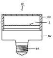
図16は、本発明のLEDランプの一例を示す断面図である。LEDランプ61は、例えば、本発明のLEDモジュール1が表面に搭載されたランプ本体62、LEDモジュール1の周囲を囲むようにランプ本体62に取り付けられる筐体部63、ランプ本体62の端部に取り付けられる口金部材64、図示しないがランプ本体62の内部に設けられる電源回路等を有する。 FIG. 16 is a cross-sectional view showing an example of the LED lamp of the present invention. The
LEDランプ61としては、必ずしも制限されないが、スポット照明用の小型のものが好ましく、例えば、最大径部分が50〜70mm程度のものが好ましい。本発明のLEDモジュール1は、指向角が小さく、大きさや厚さも抑制されていることから、LEDランプ61のより先端側に配置でき、これにより筐体部63の長さや大きさを抑制でき、また電源回路や放熱部のスペースを確保できる。このため、特にスポット照明用の小型のものに用いることで、従来と同様のスポット特性や大きさとしつつ、明るさ等を向上できる。 Although it does not necessarily restrict | limit as the
図17は、LEDランプ61を用いたスポット照明用の照明装置の一例を示す断面図である。照明装置71は、下面に開口部を有する箱状のケース本体72、このケース本体72の内部に凹部が下向きとなるように配置されるシェード部73、このシェード部73の略中央部等に配置され、LEDランプ61を取り付けるためにこのLEDランプ61の口金部材64がねじ込まれるソケット74等を有する。本発明のLEDランプ61によれば、大きさが抑制されていることから、照明装置71に適用した場合に先端部がシェード部73から突出することが抑制され、スポット特性や外観を良好にできる。 FIG. 17 is a cross-sectional view showing an example of an illumination device for spot illumination using the
本発明のLEDモジュールは、家庭用照明装置、業務用照明装置、街路灯、車載用照明装置等、特にダウンライト式およびスポットライト式照明装置に使用されるLEDランプ等に好適に使用できる。 The LED module of the present invention can be suitably used for household lighting devices, commercial lighting devices, street lamps, in-vehicle lighting devices and the like, particularly LED lamps used for downlight type and spotlight type lighting devices.
1…LEDモジュール、2…単位発光部、3…モジュール基板、4…反射板、5…搭載面、6…発光部本体、7…第1の筒状反射部、8…第2の筒状反射部、9…LED素子、11…蛍光体層、12…レンズ部、61…LEDランプ、62…ランプ本体、63…筐体部、64…口金部材、71…照明装置、72…ケース本体、73…シェード部、74…ソケット DESCRIPTION OF
Claims (11)
Translated fromJapanese前記単位発光部は、搭載面上に搭載されるLED素子および前記LED素子の主光出射側の表面を被覆する蛍光体層を有する発光部本体と、前記発光部本体の側面を囲むように設けられる第1の筒状反射部と、前記第1の筒状反射部の光出射側の端部に接続され、前記第1の筒状反射部側の端部における断面積に対して光出射側となる端部における断面積が大きい第2の筒状反射部とを有することを特徴とするLEDモジュール。An LED module having one or more unit light emitting units,
The unit light emitting unit is provided so as to surround an LED element mounted on a mounting surface, a light emitting unit main body having a phosphor layer covering a surface of the LED element on a main light emitting side, and a side surface of the light emitting unit main body. The first cylindrical reflecting portion is connected to the light emitting side end of the first cylindrical reflecting portion, and the light emitting side with respect to the cross-sectional area at the end on the first cylindrical reflecting portion side And a second cylindrical reflection portion having a large cross-sectional area at the end portion.
前記LEDモジュールが請求項1乃至10のいずれか1項記載のLEDモジュールであることを特徴とするLEDランプ。An LED lamp having a lamp body and an LED module mounted on the lamp body,
The LED module according to any one of claims 1 to 10, wherein the LED module is an LED module.
Priority Applications (1)
| Application Number | Priority Date | Filing Date | Title |
|---|---|---|---|
| JP2011089546AJP2012222304A (en) | 2011-04-13 | 2011-04-13 | Led module and led lamp |
Applications Claiming Priority (1)
| Application Number | Priority Date | Filing Date | Title |
|---|---|---|---|
| JP2011089546AJP2012222304A (en) | 2011-04-13 | 2011-04-13 | Led module and led lamp |
Publications (1)
| Publication Number | Publication Date |
|---|---|
| JP2012222304Atrue JP2012222304A (en) | 2012-11-12 |
Family
ID=47273463
Family Applications (1)
| Application Number | Title | Priority Date | Filing Date |
|---|---|---|---|
| JP2011089546AWithdrawnJP2012222304A (en) | 2011-04-13 | 2011-04-13 | Led module and led lamp |
Country Status (1)
| Country | Link |
|---|---|
| JP (1) | JP2012222304A (en) |
Cited By (7)
| Publication number | Priority date | Publication date | Assignee | Title |
|---|---|---|---|---|
| JP2013249239A (en)* | 2012-06-01 | 2013-12-12 | Nichia Corp | Substrate for placing light emitting element thereon, and light emitting device |
| JP2014517489A (en)* | 2011-06-17 | 2014-07-17 | コーニンクレッカ フィリップス エヌ ヴェ | Light emitting diode light source |
| JP2015037055A (en)* | 2013-08-14 | 2015-02-23 | 有限会社牛方商会 | Optical system device, LED module |
| JP2017502523A (en)* | 2014-01-08 | 2017-01-19 | コーニンクレッカ フィリップス エヌ ヴェKoninklijke Philips N.V. | Deep molded reflector cup used as finished LED package |
| KR20180114193A (en)* | 2016-02-26 | 2018-10-17 | 매직 립, 인코포레이티드 | Optical output system with reflector and lens for very spatially uniform light output |
| JP2019050326A (en)* | 2017-09-12 | 2019-03-28 | 株式会社フーマイスターエレクトロニクス | Led light source device having directivity for projector |
| WO2024108069A1 (en)* | 2022-11-16 | 2024-05-23 | Massachusetts Institute Of Technology | A micro-optical structure and a method for forming a micro-optical structure |
Citations (8)
| Publication number | Priority date | Publication date | Assignee | Title |
|---|---|---|---|---|
| JP2001217466A (en)* | 2000-02-03 | 2001-08-10 | Toyoda Gosei Co Ltd | Reflection-type light-emitting device |
| JP2005109382A (en)* | 2003-10-02 | 2005-04-21 | Citizen Electronics Co Ltd | Light emitting diode |
| JP2005150202A (en)* | 2003-11-12 | 2005-06-09 | Ojima Shisaku Kenkyusho:Kk | Light-emitting diode condensing device and ultraviolet irradiation device |
| JP2007123904A (en)* | 2005-10-27 | 2007-05-17 | Barco Nv | Integrated LED device with increased pixel fill factor to improve the image quality of an LED display made using the device |
| JP2007189006A (en)* | 2006-01-12 | 2007-07-26 | Hitachi Aic Inc | Printed wiring board, and led device using it |
| JP2007235079A (en)* | 2006-03-01 | 2007-09-13 | Ikuo Iwai | Light emitting device |
| WO2009028090A1 (en)* | 2007-08-31 | 2009-03-05 | Phoenix Electric Co., Ltd. | Light emitting device for illumination |
| WO2009031240A1 (en)* | 2007-09-07 | 2009-03-12 | Phoenix Electric Co., Ltd. | Self-luminous light-emitting device |
- 2011
- 2011-04-13JPJP2011089546Apatent/JP2012222304A/ennot_activeWithdrawn
Patent Citations (8)
| Publication number | Priority date | Publication date | Assignee | Title |
|---|---|---|---|---|
| JP2001217466A (en)* | 2000-02-03 | 2001-08-10 | Toyoda Gosei Co Ltd | Reflection-type light-emitting device |
| JP2005109382A (en)* | 2003-10-02 | 2005-04-21 | Citizen Electronics Co Ltd | Light emitting diode |
| JP2005150202A (en)* | 2003-11-12 | 2005-06-09 | Ojima Shisaku Kenkyusho:Kk | Light-emitting diode condensing device and ultraviolet irradiation device |
| JP2007123904A (en)* | 2005-10-27 | 2007-05-17 | Barco Nv | Integrated LED device with increased pixel fill factor to improve the image quality of an LED display made using the device |
| JP2007189006A (en)* | 2006-01-12 | 2007-07-26 | Hitachi Aic Inc | Printed wiring board, and led device using it |
| JP2007235079A (en)* | 2006-03-01 | 2007-09-13 | Ikuo Iwai | Light emitting device |
| WO2009028090A1 (en)* | 2007-08-31 | 2009-03-05 | Phoenix Electric Co., Ltd. | Light emitting device for illumination |
| WO2009031240A1 (en)* | 2007-09-07 | 2009-03-12 | Phoenix Electric Co., Ltd. | Self-luminous light-emitting device |
Cited By (17)
| Publication number | Priority date | Publication date | Assignee | Title |
|---|---|---|---|---|
| JP2014517489A (en)* | 2011-06-17 | 2014-07-17 | コーニンクレッカ フィリップス エヌ ヴェ | Light emitting diode light source |
| US9541240B2 (en) | 2011-06-17 | 2017-01-10 | Philips Lighting Holding B.V. | LED light source |
| JP2013249239A (en)* | 2012-06-01 | 2013-12-12 | Nichia Corp | Substrate for placing light emitting element thereon, and light emitting device |
| JP2015037055A (en)* | 2013-08-14 | 2015-02-23 | 有限会社牛方商会 | Optical system device, LED module |
| US11227982B2 (en) | 2014-01-08 | 2022-01-18 | Lumileds Llc | Deep molded reflector cup used as complete LED package |
| JP2017502523A (en)* | 2014-01-08 | 2017-01-19 | コーニンクレッカ フィリップス エヌ ヴェKoninklijke Philips N.V. | Deep molded reflector cup used as finished LED package |
| KR20180114193A (en)* | 2016-02-26 | 2018-10-17 | 매직 립, 인코포레이티드 | Optical output system with reflector and lens for very spatially uniform light output |
| JP2019514034A (en)* | 2016-02-26 | 2019-05-30 | マジック リープ, インコーポレイテッドMagic Leap,Inc. | Light output system with reflector and lens for highly spatially uniform light output |
| JP7007283B2 (en) | 2016-02-26 | 2022-01-24 | マジック リープ, インコーポレイテッド | Light output system with reflectors and lenses for very spatially uniform light output |
| JP2022040218A (en)* | 2016-02-26 | 2022-03-10 | マジック リープ, インコーポレイテッド | Light output system with reflector and lens for highly spatially uniform light output |
| US11378256B2 (en) | 2016-02-26 | 2022-07-05 | Magic Leap, Inc. | Light output system with reflector and lens for highly spatially uniform light output |
| JP7277619B2 (en) | 2016-02-26 | 2023-05-19 | マジック リープ, インコーポレイテッド | Light output system with reflectors and lenses for highly spatially uniform light output |
| US11692689B2 (en) | 2016-02-26 | 2023-07-04 | Magic Leap, Inc. | Light output system with reflector and lens for highly spatially uniform light output |
| KR102704208B1 (en)* | 2016-02-26 | 2024-09-05 | 매직 립, 인코포레이티드 | Light output system with reflector and lens for very spatially uniform light output |
| US12264803B2 (en) | 2016-02-26 | 2025-04-01 | Magic Leap, Inc. | Light output system with reflector and lens for highly spatially uniform light output |
| JP2019050326A (en)* | 2017-09-12 | 2019-03-28 | 株式会社フーマイスターエレクトロニクス | Led light source device having directivity for projector |
| WO2024108069A1 (en)* | 2022-11-16 | 2024-05-23 | Massachusetts Institute Of Technology | A micro-optical structure and a method for forming a micro-optical structure |
Similar Documents
| Publication | Publication Date | Title |
|---|---|---|
| JP2012222304A (en) | Led module and led lamp | |
| US20210088200A1 (en) | Light-Emitting Device and Luminaire Incorporating Same | |
| EP2623845B1 (en) | Lighting device | |
| US9903537B2 (en) | LED tube lamp | |
| EP2751472B1 (en) | Lighting device | |
| EP3161556B1 (en) | Led lighting unit | |
| EP2458266B1 (en) | Light emitting diode (LED) lamp | |
| WO2011010535A1 (en) | Led illuminator | |
| CN106463591A (en) | LED with remote phosphor and shell reflector | |
| US9200756B2 (en) | Lighting device | |
| CN102235594A (en) | Light-emitting diode (LED) light-emitting module | |
| JP2014048547A (en) | Bulk type lens, and luminous body and illuminating apparatus using the same | |
| CN204268112U (en) | Lighting device | |
| TW522751B (en) | Organic flat light emitting device | |
| KR20140095913A (en) | Light emitting module and light apparatus having thereof | |
| CN103335222B (en) | LED lamp with high light emitting efficiency | |
| KR101997250B1 (en) | Light emitting device and lighting systme having thereof | |
| CN206802819U (en) | A kind of LED light bar | |
| KR101557443B1 (en) | Lighting device | |
| CN105358898A (en) | Lighting device, lighting reflector and production method therefor | |
| CN108413264A (en) | A kind of high light-emitting rate ultraviolet LED lighting device | |
| CN205001886U (en) | Luminous LED lamp of no dark space wide -angle | |
| TWM443271U (en) | Optical element and light source module with the optical element | |
| CN104251391A (en) | LED (light-emitting diode) bulb lamp | |
| CN209101042U (en) | A kind of LED reflection type lamp |
Legal Events
| Date | Code | Title | Description |
|---|---|---|---|
| A621 | Written request for application examination | Free format text:JAPANESE INTERMEDIATE CODE: A621 Effective date:20140205 | |
| A977 | Report on retrieval | Free format text:JAPANESE INTERMEDIATE CODE: A971007 Effective date:20140625 | |
| A131 | Notification of reasons for refusal | Free format text:JAPANESE INTERMEDIATE CODE: A131 Effective date:20140708 | |
| A761 | Written withdrawal of application | Free format text:JAPANESE INTERMEDIATE CODE: A761 Effective date:20140814 |