JP2012216725A - Resistive storage device and manufacturing method thereof - Google Patents
Resistive storage device and manufacturing method thereofDownload PDFInfo
- Publication number
- JP2012216725A JP2012216725AJP2011082098AJP2011082098AJP2012216725AJP 2012216725 AJP2012216725 AJP 2012216725AJP 2011082098 AJP2011082098 AJP 2011082098AJP 2011082098 AJP2011082098 AJP 2011082098AJP 2012216725 AJP2012216725 AJP 2012216725A
- Authority
- JP
- Japan
- Prior art keywords
- memory device
- electrode
- resistance memory
- ion conductor
- resistance
- Prior art date
- Legal status (The legal status is an assumption and is not a legal conclusion. Google has not performed a legal analysis and makes no representation as to the accuracy of the status listed.)
- Withdrawn
Links
- 238000004519manufacturing processMethods0.000titleclaimsabstractdescription15
- 238000003860storageMethods0.000titleclaimsabstractdescription10
- 239000010416ion conductorSubstances0.000claimsabstractdescription83
- 239000012212insulatorSubstances0.000claimsdescription68
- 239000007784solid electrolyteSubstances0.000claimsdescription5
- 150000002500ionsChemical class0.000abstractdescription82
- 239000010949copperSubstances0.000description37
- 238000000034methodMethods0.000description25
- 229910021645metal ionInorganic materials0.000description17
- 230000015572biosynthetic processEffects0.000description12
- 230000005684electric fieldEffects0.000description12
- 229910004298SiO 2Inorganic materials0.000description10
- 239000010410layerSubstances0.000description10
- 239000002245particleSubstances0.000description9
- 229910052581Si3N4Inorganic materials0.000description7
- 238000001020plasma etchingMethods0.000description7
- HQVNEWCFYHHQES-UHFFFAOYSA-Nsilicon nitrideChemical compoundN12[Si]34N5[Si]62N3[Si]51N64HQVNEWCFYHHQES-UHFFFAOYSA-N0.000description7
- 238000004544sputter depositionMethods0.000description7
- 239000011229interlayerSubstances0.000description5
- BASFCYQUMIYNBI-UHFFFAOYSA-NplatinumChemical compound[Pt]BASFCYQUMIYNBI-UHFFFAOYSA-N0.000description5
- XUIMIQQOPSSXEZ-UHFFFAOYSA-NSiliconChemical compound[Si]XUIMIQQOPSSXEZ-UHFFFAOYSA-N0.000description4
- 229910000480nickel oxideInorganic materials0.000description4
- 229910052710siliconInorganic materials0.000description4
- 239000010703siliconSubstances0.000description4
- 239000010936titaniumSubstances0.000description4
- VYPSYNLAJGMNEJ-UHFFFAOYSA-NSilicium dioxideChemical compoundO=[Si]=OVYPSYNLAJGMNEJ-UHFFFAOYSA-N0.000description3
- 238000009826distributionMethods0.000description3
- 230000000694effectsEffects0.000description3
- 239000000463materialSubstances0.000description3
- 239000000758substrateSubstances0.000description3
- 229910052715tantalumInorganic materials0.000description3
- RYGMFSIKBFXOCR-UHFFFAOYSA-NCopperChemical compound[Cu]RYGMFSIKBFXOCR-UHFFFAOYSA-N0.000description2
- KJTLSVCANCCWHF-UHFFFAOYSA-NRutheniumChemical compound[Ru]KJTLSVCANCCWHF-UHFFFAOYSA-N0.000description2
- 239000011575calciumSubstances0.000description2
- 239000004020conductorSubstances0.000description2
- 229910052802copperInorganic materials0.000description2
- 230000006870functionEffects0.000description2
- 239000007789gasSubstances0.000description2
- 239000011777magnesiumSubstances0.000description2
- 229910052751metalInorganic materials0.000description2
- 239000002184metalSubstances0.000description2
- 238000000206photolithographyMethods0.000description2
- 238000007747platingMethods0.000description2
- 229910052697platinumInorganic materials0.000description2
- 229910052707rutheniumInorganic materials0.000description2
- 239000011669seleniumSubstances0.000description2
- GUVRBAGPIYLISA-UHFFFAOYSA-Ntantalum atomChemical compound[Ta]GUVRBAGPIYLISA-UHFFFAOYSA-N0.000description2
- 229910052719titaniumInorganic materials0.000description2
- ZOXJGFHDIHLPTG-UHFFFAOYSA-NBoronChemical compound[B]ZOXJGFHDIHLPTG-UHFFFAOYSA-N0.000description1
- OYPRJOBELJOOCE-UHFFFAOYSA-NCalciumChemical compound[Ca]OYPRJOBELJOOCE-UHFFFAOYSA-N0.000description1
- FYYHWMGAXLPEAU-UHFFFAOYSA-NMagnesiumChemical compound[Mg]FYYHWMGAXLPEAU-UHFFFAOYSA-N0.000description1
- ZOKXTWBITQBERF-UHFFFAOYSA-NMolybdenumChemical compound[Mo]ZOKXTWBITQBERF-UHFFFAOYSA-N0.000description1
- BPQQTUXANYXVAA-UHFFFAOYSA-NOrthosilicateChemical compound[O-][Si]([O-])([O-])[O-]BPQQTUXANYXVAA-UHFFFAOYSA-N0.000description1
- BUGBHKTXTAQXES-UHFFFAOYSA-NSeleniumChemical compound[Se]BUGBHKTXTAQXES-UHFFFAOYSA-N0.000description1
- BQCADISMDOOEFD-UHFFFAOYSA-NSilverChemical compound[Ag]BQCADISMDOOEFD-UHFFFAOYSA-N0.000description1
- NINIDFKCEFEMDL-UHFFFAOYSA-NSulfurChemical compound[S]NINIDFKCEFEMDL-UHFFFAOYSA-N0.000description1
- RTAQQCXQSZGOHL-UHFFFAOYSA-NTitaniumChemical compound[Ti]RTAQQCXQSZGOHL-UHFFFAOYSA-N0.000description1
- QVGXLLKOCUKJST-UHFFFAOYSA-Natomic oxygenChemical compound[O]QVGXLLKOCUKJST-UHFFFAOYSA-N0.000description1
- 229910052788bariumInorganic materials0.000description1
- DSAJWYNOEDNPEQ-UHFFFAOYSA-Nbarium atomChemical compound[Ba]DSAJWYNOEDNPEQ-UHFFFAOYSA-N0.000description1
- 229910052796boronInorganic materials0.000description1
- 229910052791calciumInorganic materials0.000description1
- 229910052798chalcogenInorganic materials0.000description1
- 150000001787chalcogensChemical class0.000description1
- 238000005229chemical vapour depositionMethods0.000description1
- 230000000052comparative effectEffects0.000description1
- 239000012141concentrateSubstances0.000description1
- AQKDYYAZGHBAPR-UHFFFAOYSA-Mcopper;copper(1+);sulfanideChemical compound[SH-].[Cu].[Cu+]AQKDYYAZGHBAPR-UHFFFAOYSA-M0.000description1
- 238000013500data storageMethods0.000description1
- 230000007547defectEffects0.000description1
- 238000010586diagramMethods0.000description1
- 238000005516engineering processMethods0.000description1
- 229910052749magnesiumInorganic materials0.000description1
- 238000007521mechanical polishing techniqueMethods0.000description1
- 150000002736metal compoundsChemical class0.000description1
- 239000002923metal particleSubstances0.000description1
- 229910052750molybdenumInorganic materials0.000description1
- 239000011733molybdenumSubstances0.000description1
- 150000004767nitridesChemical class0.000description1
- GNRSAWUEBMWBQH-UHFFFAOYSA-NoxonickelChemical compound[Ni]=OGNRSAWUEBMWBQH-UHFFFAOYSA-N0.000description1
- 229910052760oxygenInorganic materials0.000description1
- 239000001301oxygenSubstances0.000description1
- 238000005268plasma chemical vapour depositionMethods0.000description1
- 230000003252repetitive effectEffects0.000description1
- 229910052711seleniumInorganic materials0.000description1
- 229910021332silicideInorganic materials0.000description1
- FVBUAEGBCNSCDD-UHFFFAOYSA-Nsilicide(4-)Chemical compound[Si-4]FVBUAEGBCNSCDD-UHFFFAOYSA-N0.000description1
- 235000012239silicon dioxideNutrition0.000description1
- 239000000377silicon dioxideSubstances0.000description1
- 229910052814silicon oxideInorganic materials0.000description1
- 229910052709silverInorganic materials0.000description1
- 239000004332silverSubstances0.000description1
- 229910052712strontiumInorganic materials0.000description1
- CIOAGBVUUVVLOB-UHFFFAOYSA-Nstrontium atomChemical compound[Sr]CIOAGBVUUVVLOB-UHFFFAOYSA-N0.000description1
- 239000000126substanceSubstances0.000description1
- 229910052717sulfurInorganic materials0.000description1
- 239000011593sulfurSubstances0.000description1
- OGIDPMRJRNCKJF-UHFFFAOYSA-Ntitanium(II) oxideChemical compound[Ti]=OOGIDPMRJRNCKJF-UHFFFAOYSA-N0.000description1
- WFKWXMTUELFFGS-UHFFFAOYSA-NtungstenChemical compound[W]WFKWXMTUELFFGS-UHFFFAOYSA-N0.000description1
- 229910052721tungstenInorganic materials0.000description1
- 239000010937tungstenSubstances0.000description1
Images


Landscapes
- Semiconductor Memories (AREA)
Abstract
Description
Translated fromJapanese本発明は抵抗記憶装置に関し、特にイオン伝導体に金属イオンを導入、排除して導電性を変化させることで、抵抗を変化させる機能を有する抵抗記憶装置およびその製造方法に関する。 The present invention relates to a resistance memory device, and more particularly, to a resistance memory device having a function of changing resistance by introducing and removing metal ions from an ion conductor to change the conductivity, and a method of manufacturing the same.
この種の抵抗記憶装置としては、例えば、ナノブリッジ素子を抵抗記憶装置として用いてクロスバースイッチを構成するものがあった。 As this type of resistance memory device, for example, there is a device that forms a crossbar switch using a nanobridge element as a resistance memory device.
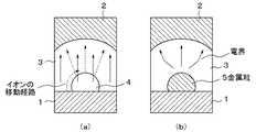
まず、抵抗記憶装置の例として、ナノブリッジ素子と呼ばれる構造について説明する。図9に非特許文献1(2010 IEEE ELECTRON DEVICES MEETING TECHNICAL DIGEST (pp.303-306))で報告されたナノブリッジ素子の例を示す。同図では、ナノブリッジ素子の断面形状と動作を示し、ルテニウム(Ru)電極101と固体電解質層102と銅(Cu)電極103とを積層した構造のナノブリッジ素子である。素子抵抗を低抵抗に変化させるには、図9(a)に示すように、Cu電極103にプラスの電圧(+V)を印加することでCuイオン(Cu+)をRu電極101へ向かう方向に移動させ、固体電解質層102内にCu導電領域132を形成して(図9(b)参照)、Cu電極103とRu電極101の間を低抵抗(ON)にする。逆に、図9(c)に示すように、Ru電極101にプラスの電圧(+V)を印加するとCuイオンがCu電極103へ向かう方向に移動してCu電極103に回収されるため、Cu電極103とRu電極101の間は高抵抗(OFF)に変化する(図9(d)参照)。このように、図9に示すナノブリッジ素子では、電圧の印加方向により抵抗を変化させることができる。First, a structure called a nanobridge element will be described as an example of a resistance memory device. FIG. 9 shows an example of a nanobridge element reported in Non-Patent Document 1 (2010 IEEE ELECTRON DEVICES MEETING TECHNICAL DIGEST (pp. 303-306)). The figure shows the cross-sectional shape and operation of the nanobridge element, which is a nanobridge element having a structure in which a ruthenium (Ru) electrode 101, a
次に、このナノブリッジ素子を用いて構成したクロスバースイッチについて図10を用いて説明する。本例では交差する2系統の配線群、例えば、ビット線B1乃至B3とワード線W1乃至W3の交差部分に両配線を接続するようにナノブリッジ素子A11乃至A33が配置されている。初期状態ではすべてのナノブリッジ素子が高抵抗の状態とする。ナノブリッジ素子A11を低抵抗にして配線B1と配線W1間を電気的接続状態にするには、B1とW1にそれぞれ電圧Vddと0Vを、その他の配線にVdd/2を印加する。Vddをナノブリッジ素子が低抵抗に変化する閾値電圧Vthより大きく、かつVdd/2がVthより小さくなるように設定することで、所望のナノブリッジ素子A11だけ低抵抗に変化させることができる。これにより所望の1対の配線B1とW1が低抵抗で接続されることになる。 Next, a crossbar switch configured using this nanobridge element will be described with reference to FIG. In this example, the nanobridge elements A11 to A33 are arranged so as to connect both wirings to two intersecting wiring groups, for example, the intersections of the bit lines B1 to B3 and the word lines W1 to W3. In the initial state, all nanobridge elements are in a high resistance state. In order to make the nanobridge element A11 have a low resistance so that the wiring B1 and the wiring W1 are electrically connected, voltages Vdd and 0V are applied to B1 and W1, respectively, and Vdd / 2 is applied to the other wirings. By setting Vdd to be larger than the threshold voltage Vth at which the nanobridge element changes to low resistance and Vdd / 2 to be lower than Vth, only the desired nanobridge element A11 can be changed to low resistance. As a result, a desired pair of wirings B1 and W1 are connected with low resistance.
配線間を電気的に切断するには逆向きの電圧−Vddを印加して、ナノブリッジ素子を高抵抗に変化させる。これらの動作により、2系統の配線群同士の接続を自由に切り替えるクロスバースイッチを構成することができる。 In order to electrically disconnect between the wirings, a reverse voltage -Vdd is applied to change the nanobridge element to a high resistance. With these operations, it is possible to configure a crossbar switch that freely switches the connection between two wiring groups.
ほかの抵抗記憶装置の例として、特許文献1、2、3に開示されているような例がある。その一例として、特許文献1(特開2009−212380)で示された抵抗記憶装置について図11を用いて示す。この抵抗記憶装置では、一対の電極間に抵抗変化層を挟んだ構造であるが、この抵抗変化層は、多結晶酸化物膜と、これよりも厚いアモルファス酸化物膜との積層を含んでいる。下部電極110としては白金(Pt)50nm、多結晶酸化物膜111としては多結晶酸化ニッケル(NiO)を5nm、アモルファス酸化物膜112としてはアモルファスNiOを10nm、上部電極113としてはPt50nmを使用している。動作方法は図9と同様であるが、本構造により、抵抗記憶装置を微細化しても、初期短絡不良を防ぎつつ、フィラメント114を形成して抵抗変化を開始させるフォーミング電圧を低く維持することができるとしている。 Examples of other resistance memory devices include those disclosed in
このような抵抗記憶装置は、前述のような電気的接続経路を切り替えるスイッチ用途や、データを記憶するメモリ用途などに用いられる。 Such a resistance memory device is used for a switch for switching an electrical connection path as described above, a memory for storing data, and the like.
特許文献1では、抵抗変化層としてNiOや酸化チタン(TiO)を用いた関連技術の抵抗記憶装置の研究において、抵抗記憶装置特性のばらつきが大きく、抵抗記憶装置面積を小さくするとフォーミング電圧が大きくなるという問題が明らかになったとしている。そして、面積依存性については、成膜後の抵抗記憶装置中に存在するウイークスポットの程度と存在確率が変わるためとしている。 In
特許文献1ではこの問題を解決する方法として、グレインバウンダリ115に電界が集中しやすいことを利用し、多結晶酸化物膜を用い、そのグレインバウンダリを起点としてフォーミングを生じさせている。グレインを抵抗記憶装置サイズより小さくすることで、抵抗記憶装置内に多数のグレインバウンダリ115、すなわちフォーミングの起点を設けることで、微細化による起点の減少から起こるフォーミング電圧の増大を防ぐとしている。 In
さて、もう一つの問題である抵抗記憶装置特性のばらつきであるが、(1)抵抗記憶装置間のばらつきと(2)同一抵抗記憶装置での繰り返しばらつきの2種類が考えられる。抵抗記憶装置間ばらつきについては、前述の起点の減少による個体差や、フィラメントが形成される電極の表面形状の抵抗記憶装置間の違いが原因となる。ここで電極の表面形状の影響について図12を用いて説明する。 There are two types of resistance memory device variations, which are another problem. There are two types: (1) variations between resistance memory devices and (2) repeated variations in the same resistance memory device. The variation between the resistance memory devices is caused by the individual difference due to the decrease in the starting point and the difference between the resistance memory devices in the surface shape of the electrode on which the filament is formed. Here, the influence of the surface shape of the electrode will be described with reference to FIG.
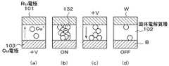
図12は、電極表面形状が異なる3つの抵抗記憶装置R1、R2、R3についてフィラメント114が形成される位置を示した断面図である。図12(a)に示す抵抗記憶装置R1は、その電極103の表面が平坦な場合である。図12(b)および(c)に示す抵抗記憶素子R2およびR3は、その電極103の表面に異なる凹凸がある場合を示している。 FIG. 12 is a cross-sectional view showing the positions where the
さらに図12には、書き込みを3回行い、フィラメント形成を繰り返し行ったときのフィラメント114の形成位置の変化を縦方向に1回目、2回目、3回目として示してある。抵抗記憶装置R2と抵抗記憶装置R3では表面形状が異なっており、突部の高さや鋭さで電界集中の程度が変わっている。電界強度はフィラメント形成に寄与するため、抵抗記憶装置R2と抵抗記憶装置R3とでは書き込み特性が異なることになり、電極表面形状が抵抗記憶装置間のばらつきに影響するのは明らかである。 Further, FIG. 12 shows the change in the formation position of the
次に、繰り返し書き込み時の特性ばらつきについては、以下のように考える。抵抗記憶装置R1のように電極103を平坦化した場合、フィラメント114が形成される確率はどこでも同程度であり、図12(a)に示すように書き込むたびに異なる場所に形成されると考えられる。電極103の平坦化は、抵抗変化層102を薄膜化して動作の低電圧化をはかる上で、膜内の欠陥形成を抑制するために必要であるが、抵抗変化層102を完全に均質にすることは難しく、フィラメント114の太さや形状や形成電圧は形成される位置に影響を受けることは明らかである。 Next, characteristic variations at the time of repeated writing are considered as follows. When the
一方、抵抗記憶装置R2や抵抗記憶装置R3のように電極103が平坦でなく突部がある場合は、繰り返して書き込みを行っても図12(b)および(c)に示すように、同じ場所にフィラメント114が形成される確率が高く、繰り返しばらつきは小さいと考えられる。しかし、電極自体がイオン化して移動するため、動作を繰り返すと形状が経時変化し、フィラメント形成点が移動する可能性がある。これらのような現象が繰り返しばらつきに影響すると考えられる。 On the other hand, when the
この問題に対し特許文献1に開示の構造を適用した場合、膜上方からみるとグレインバウンダリは網目状に全面につながっており、その上面は下部電極の表面形状を反映する。このため、前述の2つのばらつきに対しての改善効果はほとんどないことは明らかである。 When the structure disclosed in
このように、特許文献1では下部電極表面形状に起因して特性がばらつくため、すべてのセルを書き込むためにはマージンを考慮した高い書き込み電圧が必要となり、消費電力が低減できないという問題があった。 As described above, in
本発明の目的は、上述した課題を解決した抵抗記憶装置およびその製造方法を提供することにある。 An object of the present invention is to provide a resistance memory device that solves the above-described problems and a method of manufacturing the same.
本発明の抵抗記憶装置は、イオン源部材と、イオン源部材上に形成された粒状または島状の絶縁体部材と、絶縁体部材上に形成されたイオン伝導体部材と、イオン伝導体部材上に形成された電極部材とを有することを特徴とする。 The resistance memory device of the present invention includes an ion source member, a granular or island-shaped insulator member formed on the ion source member, an ion conductor member formed on the insulator member, and an ion conductor member It has the electrode member formed in this.
また、本発明の抵抗記憶装置の製造方法は、イオン源部材上に粒状または島状に絶縁部材を形成する工程と、この絶縁部材上にイオン伝導体部材を形成する工程と、イオン伝導体部材上に電極部材を形成する工程とを有することを特徴とする。 The method of manufacturing a resistance memory device of the present invention includes a step of forming an insulating member in a granular or island shape on an ion source member, a step of forming an ion conductor member on the insulating member, and an ion conductor member. Forming an electrode member thereon.
この発明によれば、特性ばらつきが改善されてマージン電圧を小さくできるため低い電圧での書き込みが可能となり、低消費電力の抵抗記憶装置が実現できる。 According to the present invention, the variation in characteristics can be improved and the margin voltage can be reduced, so that writing at a low voltage is possible, and a low power consumption resistance memory device can be realized.
(b) 比較参考例の動作説明のための概略断面図である。
本発明の実施の形態につき図面を参照して説明する。 Embodiments of the present invention will be described with reference to the drawings.
図1を参照すると、本発明の第一の実施の形態として抵抗記憶装置の要部概略断面図が示されている。 Referring to FIG. 1, a schematic cross-sectional view of a main part of a resistance memory device is shown as a first embodiment of the present invention.
第一の実施の形態の抵抗記憶装置は、図1に示すように、第1のイオン源1と、第1の電極2と、第1のイオン伝導体3と、第1の絶縁体4とを有する。第1のイオン源1と第1の電極2は、第1のイオン伝導体3を挟んで配置される。第1の絶縁体4は、第1のイオン伝導体3と接する第1のイオン源1の表面に配置される。さらに第1の絶縁体4は、粒形状または島形状を有する。すなわち、第1のイオン伝導体3は、第1のイオン源1と第1の絶縁体4との両方に面する領域を有する。 As shown in FIG. 1, the resistance memory device according to the first embodiment includes a
次に本抵抗記憶装置の動作について図2を用いて説明する。図2(a)を参照すると、本発明の第一の実施の形態の要部断面が示されている。まず、本抵抗記憶装置の第1のイオン源1と第1の電極2との間の抵抗値を、高抵抗から低抵抗に変化させる書き込み方法について説明する。 Next, the operation of the resistance memory device will be described with reference to FIG. Referring to FIG. 2 (a), a cross section of the main part of the first embodiment of the present invention is shown. First, a writing method for changing the resistance value between the
高抵抗状態では、図2(a)に示すように第1のイオン伝導体3には金属イオンがほとんど存在せず、第1のイオン源1と第1の電極2との間にはほとんど電流が流れない。ここで第1のイオン源1と第1の電極2との間に、イオン源1の金属イオンが第1の電極2の方向に流れる第1の極性で所望の値の電圧を所望の時間印加する。このとき、電界は導電体である第1のイオン源1と第1の電極2との間に形成されるため、まず金属イオンは移動しやすい第1のイオン伝導体3と第1の絶縁体4との界面を移動する。そして図2(a)の点線の矢印で示すように第1のイオン伝導体3を通り、第1の電極2に向けてフィラメントを形成する。このようにして、低抵抗に変化させる。 In the high resistance state, as shown in FIG. 2 (a), almost no metal ions are present in the
次に、低抵抗から高抵抗に変化させる書き込み方法について説明する。第1のイオン源1と第1の電極2との間に、第1の極性とは逆向きで所望の値の電圧を所望の時間印加する。これにより、第1のイオン伝導体3内の金属イオンが第1のイオン源1の方向に移動する。さらに、第1のイオン伝導体1と第1の絶縁体4との界面では、金属イオンが移動しやすいため、金属イオンが第1のイオン源1に回収される。このようにして第1のイオン伝導体3に金属イオンが存在しなくなるため、高抵抗を示すようになる。 Next, a writing method for changing from low resistance to high resistance will be described. A voltage having a desired value is applied between the
次に、本抵抗記憶装置の読み出し方法について説明する。読み出しは第1のイオン源1と第1の電極2との間の抵抗を評価することで行う。たとえば、第1のイオン源1に電圧を印加して第1の読み出し端子1と第2の読み出し端子2との間に電位差を与えることにより、第1の電極2を充電し、一定時間後の第1の電極2の電位と所望の電位とをセンスアンプを用いて比較する。ほかには、定電流源から所望の電流を流したときの電位と所望の電位とをセンスアンプを用いて比較するなどの方法がある。 Next, a reading method of the resistance memory device will be described. Reading is performed by evaluating the resistance between the
第1のイオン伝導体に薄い部分があると、電界が強くなるためフィラメントが形成されやすくなる。これは、繰り返し書き込み時に同じ場所にフィラメントが形成されることになるため、繰り返し書き込み特性が安定することを意味する。 If the first ion conductor has a thin portion, the electric field becomes strong, so that a filament is easily formed. This means that since the filament is formed at the same place during repeated writing, the repeated writing characteristic is stabilized.
凹凸に対し均一な膜厚となる成膜方法でも、第1のイオン伝導体3が薄いと粒に沿って一様な膜厚で形成されるが、厚くなるにつれ第1の絶縁体4の上部が薄く、それ以外が厚くなる傾向がある。このため、第1のイオン伝導体3の厚さは第1の絶縁体4の粒の大きさに比べ、厚いほうが望ましい。凹凸があっても平坦な膜が形成できる成膜方法では、第1の絶縁体4上部の第1のイオン伝導体3が薄くなるので、この限りではない。また、フィラメントの形成確率が第1のイオン源表面の凹凸ではなく、粒のサイズ分布に支配される必要があるため、粒サイズのばらつきを第1のイオン源表面の凹凸ばらつきより大きくする必要がある。 Even when the
また、図2(b)に、絶縁体粒ではなく金属粒5を用いた場合について説明する。この場合、書き込み時の電界は、金属粒最頂部で終端してしまい、第1のイオン源1近傍では電界がほとんどなくなってしまう。このため、金属イオンが移動しにくい。このことから、絶縁体粒のほうがフィラメント形成に適している。イオン源は、イオン化量を調整するためイオン源と第1のイオン伝導体3および/または第1の絶縁体4との間にイオン源以外の材料を挟んでも良い。 In addition, FIG. 2B illustrates a case where metal particles 5 are used instead of insulator particles. In this case, the electric field at the time of writing is terminated at the top of the metal grains, and the electric field is almost lost in the vicinity of the
書き込み時に印加する電圧は矩形波であっても、印加中に変化する波形であってもよく、電位を変えて複数回印加しても良い。第1の絶縁体4の粒は、孤立した粒でなくても、いくつかの粒がつながった島状でも、第1のイオン伝導体3と第1のイオン源1が接する領域さえあれば同様の効果が得られる。 The voltage applied at the time of writing may be a rectangular wave, a waveform that changes during application, or may be applied multiple times by changing the potential. The grain of the
本実施の形態では、フィラメント形成点となる確率は主に書き込み電界の強さに依存するため、第1のイオン伝導体1の薄さ、すなわち第1の絶縁体4の粒の大きさで決まる。このため、第1のイオン源1と第1の電極2とが対向する領域の中で、もっとも大きい第2の絶縁体4の粒、およびこれに近い条件の粒からフィラメントが形成されやすくなる。フィラメントの形成点が絞られることにより、繰り返し書き込みを行ったときのばらつきが低減される。 In the present embodiment, since the probability of being a filament formation point mainly depends on the strength of the writing electric field, it is determined by the thinness of the
さらに、第1の絶縁体4を複数の抵抗記憶装置にわたり一様に形成することで、各抵抗記憶装置内に多数、たとえば10以上、できれば100以上の粒を設けることで、それぞれの抵抗記憶装置の粒サイズ分布を同様にすることができる。この結果、フィラメントの形成条件が抵抗記憶装置によらず同程度となり、抵抗記憶装置間の書き込み特性ばらつきを低減することができる。これにより、必要なマージン電圧が小さくなり、書き込み電圧を低減できる抵抗記憶装置を得ることができる。これらを複数用いて回路制御することで、メモリ抵抗記憶装置やスイッチ抵抗記憶装置を構成することができる。 Further, by forming the
図3を参照すると、本発明の第二の実施の形態として抵抗記憶装置の要部断面図が示されている。 Referring to FIG. 3, a cross-sectional view of the main part of a resistance memory device is shown as a second embodiment of the present invention.
第二の実施の形態の抵抗記憶装置は、図3に示すように、第1のイオン源1と、第1の電極2と、第1のイオン伝導体3と、第1の絶縁体4とを有する。第1のイオン源1と第1の電極2は、第1のイオン伝導体3を挟んで対向して配置される。第1の絶縁体4は、第1のイオン伝導体3と接する第1のイオン源1の表面に配置される。さらに第1の絶縁体4は、粒形状を有する。すなわち、第1のイオン源1と第1のイオン伝導体3とは接する領域を有する。さらに、第1の読み出し電極6と第2の読み出し電極7とを有する。読み出し電極は、第1のイオン伝導体3に接して形成される。 As shown in FIG. 3, the resistance memory device according to the second embodiment includes a
次に、本抵抗記憶装置の動作について説明する。まず、本抵抗記憶装置の読み出し方法であるが、読み出し端子間の抵抗を評価することで行う。次に、本抵抗記憶装置の読み出し電極間の抵抗を、高抵抗から低抵抗に変化させる書き込み方法について説明する。 Next, the operation of the resistance memory device will be described. First, the reading method of the resistance memory device is performed by evaluating the resistance between the reading terminals. Next, a writing method for changing the resistance between the reading electrodes of the resistance memory device from high resistance to low resistance will be described.
高抵抗状態では、図3に示すように第1のイオン伝導体3には金属イオンがほとんど存在せず、読み出し電極間にはほとんど電流が流れない。ここで第1のイオン源1と第1の電極2との間に、イオン源1の金属イオンが第1の電極2の方向に流れる第1の極性で所望の値の電圧を所望の時間印加する。このとき、電界は導電体である第1のイオン源1と第1の電極2との間に形成されるため、まず金属イオンは移動しやすい第1のイオン伝導体3と第1の絶縁体4との界面を移動する。次に、第1のイオン伝導体3を通り、第1の電極2に向けてフィラメントを形成する。このとき、第1の読み出し電極6と第2の読み出し電極7との間に電圧を印加すると、フィラメント部分を介して電子がトンネルするようになるため、電流が流れるようになる。このようにして、読み出し電極6、7間を低抵抗に変化させる。 In the high resistance state, as shown in FIG. 3, there are almost no metal ions in the
次に、低抵抗から高抵抗に変化させる書き込み方法について説明する。第1のイオン源1と第1の電極2との間に、第1の極性とは逆向きで所望の値の電圧を所望の時間印加する。これにより、第1のイオン伝導体3内の金属イオンが第1のイオン源1の方向に移動する。さらに、第1のイオン伝導体1と第1の絶縁体4との界面では、金属イオンが移動しやすいため、金属イオンが第1のイオン源1に回収される。このようにして第1のイオン伝導体3に金属イオンが存在しなくなるため、読み出し電極6、7間は高抵抗を示すようになる。 Next, a writing method for changing from low resistance to high resistance will be described. A voltage having a desired value is applied between the
それぞれの読み出し電極6、7は第1のイオン源1や第1の電極2と共用しても良い。読み出し電極間の電流は、フィラメントまでをトンネルして流れるため、第1のイオン伝導体3の厚さ、電極サイズは、所望の電流量から設計する。 Each of the
本実施の形態では、書き込み電流経路と読み出し電流経路とが異なるため、読み出しにより金属イオンが移動しても抵抗値への影響が小さく、誤書き込みが発生しにくいという特徴がある。 In this embodiment, since the write current path and the read current path are different, the influence on the resistance value is small even if the metal ions move due to the read, and erroneous writing hardly occurs.
絶縁体粒の大きさの目安について図4を用いて説明する。一辺xで正方形の抵抗記憶装置に、半径rの絶縁体粒を並べたときの平面概要図を図4(a)に、一部の断面図を図4(b)に示す。抵抗記憶装置内にy個の半球状の絶縁体粒が並んでいるとすると、絶縁体粒の直径2rは式(1)で、また抵抗記憶装置全体でみた絶縁体の平均膜厚hは式(2)で表現される。一方、第1のイオン伝導体の厚さtは、絶縁体粒の半径以上とすると、式(3)で表現される。 The standard of the size of the insulator grains will be described with reference to FIG. FIG. 4A shows a schematic plan view when insulating particles having a radius r are arranged in a square resistance memory device with one side x, and FIG. 4B shows a partial cross-sectional view. Assuming that y hemispherical insulator particles are arranged in the resistance memory device, the
2r=(x2/y)0.5(1)
h=πr/6 (2)
t=6h/π (3)2r = (x2 / y)0.5 (1)
h = πr / 6 (2)
t = 6h / π (3)
一辺が0.2μmの正方形の抵抗記憶装置内に100個の絶縁体粒を設けることを仮定すると、絶縁体粒の直径は20nm、その平均膜厚は5.2nmとなる。ここでは整列した状態を仮定しているため、実際にこの条件下では隣接する粒がつながり部分的に島が形成されている状態になると考える。 Assuming that 100 insulator grains are provided in a square resistance memory device having a side of 0.2 μm, the diameter of the insulator grains is 20 nm and the average film thickness is 5.2 nm. In this case, since the aligned state is assumed, it is considered that an island is partially formed by connecting adjacent grains under this condition.
次に、具体的な実施例を用いて本発明の動作を説明する。
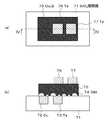
図5に示した抵抗記憶装置を用いて、本発明の第一の実施例を説明する。図5(a)は抵抗記憶装置の平面図、(b)は(a)におけるI−I線に沿った断面図である。Next, the operation of the present invention will be described using specific examples.
A first embodiment of the present invention will be described using the resistance memory device shown in FIG. FIG. 5A is a plan view of the resistance memory device, and FIG. 5B is a cross-sectional view taken along line II in FIG.
本発明の第一の実施例は、第1の電極部材であるルテニウム(Ru)56と、イオン源部材である銅(Cu)52と、イオン伝導体部材である珪酸タンタル(TaSiO)55と、イオン源部材の表面に形成された粒状または島状の絶縁体部材である二酸化シリコン(SiO2)54とを有している。第1の電極56とイオン源52は制御回路と電気的に接続されている。In the first embodiment of the present invention, ruthenium (Ru) 56 as a first electrode member, copper (Cu) 52 as an ion source member, tantalum silicate (TaSiO) 55 as an ion conductor member, And a silicon dioxide (SiO2 ) 54 which is a granular or island-shaped insulator member formed on the surface of the ion source member. The
次に、本実施例の製造方法について図6を用いて説明する。図6(a)および(c)は、代表的な製造行程における平面図であり、図6(b)および(d)は図6(a)および(c)におけるII−II線およびIII−III線に沿った断面図である。まず、集積回路などが形成されたシリコンなどの基板(図示略)上に絶縁膜としてSiO2層間膜51を400nmの厚さに成膜し、フォトリソグラフィ技術によりイオン源形成部以外をレジスト(図示略)で保護し、反応性イオンエッチング技術(以降RIEと称す)によりSiO2層間膜51を200nmの深さにエッチングする。Next, the manufacturing method of a present Example is demonstrated using FIG. 6 (a) and 6 (c) are plan views in a typical manufacturing process, and FIGS. 6 (b) and 6 (d) are taken along lines II-II and III-III in FIGS. 6 (a) and 6 (c). It is sectional drawing along a line. First, an SiO2 interlayer film 51 having a thickness of 400 nm is formed as an insulating film on a substrate such as silicon (not shown) on which an integrated circuit or the like is formed, and a resist (not shown) other than the ion source forming portion is formed by photolithography. The SiO2 interlayer film 51 is etched to a depth of 200 nm by a reactive ion etching technique (hereinafter referred to as RIE).
レジスト除去後、全面にシード層(図示略)とイオン源52となるCuを300nmの厚さにスパッタリング法とメッキ法を用いて形成した後、化学的機械的研磨技術(以降CMPと称す)により平坦化することでイオン源52部分にCuを残す。全面に絶縁膜53としてのSiO2を化学蒸着法(CHEMICAL VAPOR DEPOSITION)法(以降CVDと称す)で50nmの厚さに成膜する。抵抗記憶装置を形成する領域以外をレジストで保護し、SiO2絶縁膜53を除去し、イオン源52(Cu)を露出させる。レジスト除去後、全面に粒状絶縁体54となるSiO2をスパッタリング法で0.8nmの厚さに成膜する(図6(a) および(b))。After removing the resist, a seed layer (not shown) and Cu serving as the
成膜工程において、スパッタ時のエネルギーを下げたり、ガス圧をあげたり、低温で成膜することで、その膜は粒状になりやすくなる。前もってパラメータを調整して評価し、所望のサイズとサイズばらつきの粒を形成する条件を用いる。 In the film formation process, the film tends to become granular by lowering the energy during sputtering, increasing the gas pressure, or forming the film at a low temperature. The parameters are adjusted and evaluated in advance, and conditions for forming grains having a desired size and size variation are used.
次に、全面にイオン伝導体55(TaSiO)を10nm、第1の電極56(Ru)を20nmの厚さに、スパッタリング法で成膜する。次に、抵抗記憶装置となる領域にレジストを形成し、第1の電極56、イオン伝導体55をRIEにより除去する(図6(c)および(d))。これにより、抵抗記憶装置を形成する。 Next, the ion conductor 55 (TaSiO) is deposited to a thickness of 10 nm and the first electrode 56 (Ru) is deposited to a thickness of 20 nm on the entire surface by sputtering. Next, a resist is formed in a region to be a resistance memory device, and the
次に、本実施例の動作方法について説明する。まず、記憶状態の読み出し方法について説明する。記憶状態は、第1の電極56(Ru)とイオン源52(Cu)との間の抵抗として記憶される。このため、第1の電極56とイオン源52との間に電圧を印加して流れる電流を評価したり、定電流を流すための印加電圧を評価したりすることで、抵抗値を評価して記憶状態を判別する。メモリなどのようにデータ記憶抵抗記憶装置として用いる場合は、読み出した抵抗値からデータを判別する。また、クロスバースイッチのような用途では、抵抗値により接続、非接続として働くように回路を構成する。 Next, the operation method of the present embodiment will be described. First, a storage state reading method will be described. The memory state is stored as a resistance between the first electrode 56 (Ru) and the ion source 52 (Cu). For this reason, the resistance value is evaluated by evaluating the flowing current by applying a voltage between the
次に、抵抗記憶装置の抵抗値を高抵抗から低抵抗に変化させる書き込み方法について説明する。第1の電極56(Ru)を接地し、イオン源52(Cu)に正の電位、たとえば2Vを10ns印加する。電界はイオン源52の表面に印加するため、Cuの正イオン(Cu+)はイオン伝導体55(TaSiO)内を移動するが、特にイオン伝導体55と粒状絶縁体54の界面が移動しやすく、粒状絶縁体54の周りに広がる。さらに、イオン伝導体55を通ってフィラメントが形成される。特に抵抗記憶装置全体で粒状絶縁体54の粒部材の外径が大きく、イオン伝導体55が薄くなっている部分で電界が最も大きくなるため、この部分を通ってフィラメントが形成される確率が高い。フィラメントの形成により、低抵抗を示すようになる。Next, a writing method for changing the resistance value of the resistance memory device from high resistance to low resistance will be described. The first electrode 56 (Ru) is grounded, and a positive potential, for example, 2 V is applied to the ion source 52 (Cu) for 10 ns. Since an electric field is applied to the surface of the
次に、抵抗記憶装置の抵抗値を低抵抗から高抵抗に変化させる書き込み方法について説明する。イオン源52(Cu)を接地し、第1の電極56(Ru)に正の電位、たとえば3Vを1μs印加する。Cuイオンはイオン源52方向に移動するため、フィラメントは切断される。特に、イオン伝導体55(TaSiO)と粒状絶縁体54(SiO2)の界面では移動しやすい。このようにして、イオン伝導体内にCuイオンがなくなるため、高抵抗を示すようになる。Next, a writing method for changing the resistance value of the resistance memory device from low resistance to high resistance will be described. The ion source 52 (Cu) is grounded, and a positive potential, for example, 3 V is applied to the first electrode 56 (Ru) for 1 μs. Since the Cu ions move toward the
イオン伝導体は、本実施例のように固体電解質や、膜内に空気との界面をもつポーラスSiO2などの材料、およびこれらの積層構造も利用可能である。本実施例では、イオン源52(Cu)と第1の電極56(Ru)は直接イオン伝導体55(TaSiO)に接しているが、たとえばチタン(Ti)やSiO2などの金属や絶縁体を介して、イオン化を調整することも可能である。また、粒状絶縁体54は粒状としたが、粒同士がくっつき島状になったものが含まれても、イオン源52が露出する限りは、粒の凹凸が残るため同様の効果が得られる。As the ion conductor, a solid electrolyte, a material such as porous SiO2 having an interface with air in the film, and a laminated structure thereof can be used as in this embodiment. In this embodiment, the ion source 52 (Cu) and the first electrode 56 (Ru) are in direct contact with the ion conductor 55 (TaSiO). For example, a metal or insulator such as titanium (Ti) or SiO2 is used. It is also possible to adjust the ionization. Further, although the
本実施例によれば、フィラメントが形成される場所が絞られ、繰り返し書き込み時の書き込み特性ばらつきが抑制される。また、抵抗記憶装置間のフィラメントの形成しやすさの分布も同程度となるため、抵抗記憶装置間のばらつきも抑制される。これにより、書き込み時のマージンを小さくすることができるため、小さい書き込み電圧での利用が可能な抵抗記憶装置が得られる。 According to the present embodiment, the place where the filament is formed is narrowed down, and the variation in write characteristics during repetitive writing is suppressed. In addition, since the distribution of the ease of forming the filaments between the resistance memory devices is almost the same, the variation between the resistance memory devices is also suppressed. Thereby, the margin at the time of writing can be reduced, so that a resistance memory device that can be used with a small writing voltage can be obtained.
図7に示した抵抗記憶装置を用いて、本発明の第二の実施例を説明する。図7(a)は抵抗記憶装置の平面図、図7(b)は(a)におけるIV−IV線に沿った断面図である。 A second embodiment of the present invention will be described using the resistance memory device shown in FIG. FIG. 7A is a plan view of the resistance memory device, and FIG. 7B is a cross-sectional view taken along line IV-IV in FIG.
本発明の第二の実施例は、第1の電極77であるタンタル(Ta)と、イオン源72であるCuと、イオン伝導体75である硫化銅(Cu2S)と、イオン源表面に形成された絶縁体粒、すなわち粒状絶縁体74としての窒化シリコン(SiN)とを有している。また、第1の読み出し電極73としてのTa電極と第2の読み出し電極76としてのTa電極とを有している。各電極とイオン源は制御回路と電気的に接続されている。In the second embodiment of the present invention, tantalum (Ta) as the
次に、本実施例の製造方法について図8を用いて説明する。図8(a)および(c)は、代表的な製造行程における平面図であり、図8(b)および(d)は図8(a)および(c)におけるV−V線およびVI−VI線に沿ったそれぞれの断面図である。 Next, the manufacturing method of a present Example is demonstrated using FIG. 8 (a) and 8 (c) are plan views in a typical manufacturing process, and FIGS. 8 (b) and 8 (d) show the VV line and VI-VI in FIGS. 8 (a) and 8 (c). It is each sectional drawing along a line.
まず、集積回路などが形成されたシリコン基板等の基板(図示略)上に絶縁体(SiO2)層間膜71を400nmの厚さに成膜し、フォトリソグラフィ技術により第1の読み出し電極73(Ta)の形成部以外をレジスト(図示略)で保護し、RIEにより絶縁体層間膜71を200nmの深さまでエッチングする。レジスト除去後、全面にスパッタリング法により第1の読み出し電極73となるTaを300nmの厚さに形成した後、CMPにより平坦化することで第1の読み出し電極73のパターンを形成する。First, an insulator (SiO2 )
次に、イオン源形成部以外をレジスト(図示略)で保護し、RIEにより絶縁体層間膜71を200nmの深さまでエッチングする。レジスト除去後、全面にシード層とイオン源72となるCuを合計厚さ300nmとなるようスパッタリング法とメッキ法を用いて形成した後、CMPにより平坦化することでイオン源72の部分にCuを残す。その後、全面に粒状絶縁体74となるSiNをプラズマCVD法で0.3nmの厚みに成膜する(図8(a)および(b))。 Next, the portion other than the ion source forming portion is protected with a resist (not shown), and the insulating
成膜工程において、プラズマエネルギーを下げたり、ガス圧をあげたり、低温で成膜することで、SiN膜は粒状になりやすくなる。前もってパラメータを調整して評価し、所望のサイズとサイズばらつきの粒を形成する条件を用いる。 In the film forming process, the SiN film is likely to be granular by lowering the plasma energy, increasing the gas pressure, or forming the film at a low temperature. The parameters are adjusted and evaluated in advance, and conditions for forming grains having a desired size and size variation are used.
次に、全面にイオン伝導体75となるCu2S膜を4nm厚、上部電極となるTa膜を50nm厚となるようにスパッタリング法で順次成膜する。次に、上部電極となるTa膜をレジスト(図示略)で保護し、RIEによりTa膜を選択除去し、第2の読み出し電極76としてのTa電極と第1の電極77としてのTa電極を同時に形成する。さらに、抵抗記憶装置となる領域上にレジスト(図示略)を形成し、イオン伝導体75(Cu2S)と粒状絶縁体74(SiN)をRIEにより選択除去する(図8(c)および(d))。このようにして、抵抗記憶装置が形成される。Next, a Cu2 S film serving as the
次に、本実施例の動作方法について説明する。まず、記憶状態の読み出し方法について説明する。記憶状態は、第1の読み出し電極73(Ta)と第2の読み出し電極76(Ta)との間の抵抗値として記憶される。このため、両読み出し電極間に電圧を印加して流れる電流を評価したり、定電流を流すための印加電圧を評価したりすることで、抵抗値を評価して記憶状態を判別する。 Next, the operation method of the present embodiment will be described. First, a storage state reading method will be described. The memory state is stored as a resistance value between the first readout electrode 73 (Ta) and the second readout electrode 76 (Ta). For this reason, the resistance value is evaluated to discriminate the memory state by evaluating the flowing current by applying a voltage between both readout electrodes or by evaluating the applied voltage for flowing a constant current.
次に、抵抗記憶装置抵抗を高抵抗から低抵抗に変化させる書き込み方法について説明する。第1の電極77(Ta)を接地し、イオン源72(Cu)に正の電位、たとえば2Vを100ns印加する。Cuの正イオン(Cu+)はイオン源72からイオン伝導体75(Cu2S)内を移動するが、特にイオン伝導体75と粒状絶縁体74の界面が移動しやすく、粒状絶縁体74の粒の周りに広がる。さらに、イオン伝導体75を通って第1の電極77に向かうフィラメントが形成される。特に抵抗記憶装置全体の中で粒状絶縁体74の粒径が大きく、第1の電極77と粒状絶縁体74との距離が近い部分で電界が最も大きくなるため、この部分を通ってフィラメントが形成される確率が高い。フィラメントの形成により、第1の読み出し電極73と第2の読み出し電極76との間にフィラメントを介してトンネル電流が流れるようになるため低抵抗を示すようになる。Next, a writing method for changing the resistance memory device resistance from high resistance to low resistance will be described. The first electrode 77 (Ta) is grounded, and a positive potential, for example, 2 V is applied to the ion source 72 (Cu) for 100 ns. Cu positive ions (Cu+ ) move from the
次に、抵抗記憶装置の抵抗値を低抵抗から高抵抗に変化させる書き込み方法について説明する。イオン源72(Cu)を接地し、第1の電極77(Ta)に正の電位、たとえば3Vを10μs印加する。Cuイオンはイオン源72へ向かう方向に移動するため、フィラメントは切断される。特に、イオン伝導体75(Cu2S)と粒状絶縁体74(SiN)の界面では移動しやすい。このようにして、イオン伝導体内にCuイオンがなくなるため、高抵抗を示すようになる。Next, a writing method for changing the resistance value of the resistance memory device from low resistance to high resistance will be described. The ion source 72 (Cu) is grounded, and a positive potential, for example, 3 V is applied to the first electrode 77 (Ta) for 10 μs. Since the Cu ions move in the direction toward the
低抵抗時、読み出し電流はフィラメントを介して電子がイオン伝導体をトンネルするため、イオン伝導体は薄い必要がある。たとえばイオン伝導体厚さが4nm以下になるようにする。 When the resistance is low, the readout current must be thin because electrons tunnel through the ionic conductor through the filament. For example, the ion conductor thickness is set to 4 nm or less.
本実施例によれば、書き込み電流経路と読み出し電流経路が異なるため、読み出し電流による誤書き込みは起こりにくい。 According to this embodiment, since the write current path and the read current path are different, erroneous writing due to the read current hardly occurs.
以上の実施例において、電極を構成する材料としてはTi,Ta,Pt,タングステン(W),モリブデン(Mo),シリサイドなどがあげられる。また、イオン源としてはCu,銀(Ag),鉛(Pb)などが利用できる。イオン伝導体としては、カルコゲン元素(酸素(O),硫黄(S),セレン(Se),テリウム(Te))と金属の化合物、シリコンを含む絶縁物(酸化シリコン、窒化シリコン、酸窒化シリコン)、ペロブスカイト型酸化物(ABO3:A:マグネシウム(Mg),カルシウム(Ca),ストロンチウム(Sr),バリウム(Ba)、ホウ素(B):Ti)などでもよい。絶縁体としては、酸化物、窒化物、酸窒化物やイオン伝導体などが利用できる。In the above embodiments, examples of the material constituting the electrode include Ti, Ta, Pt, tungsten (W), molybdenum (Mo), and silicide. Moreover, Cu, silver (Ag), lead (Pb), etc. can be utilized as an ion source. Examples of ion conductors include chalcogen elements (oxygen (O), sulfur (S), selenium (Se), and terium (Te)) and metal compounds, and insulators containing silicon (silicon oxide, silicon nitride, silicon oxynitride). Perovskite oxide (ABO3 : A: magnesium (Mg), calcium (Ca), strontium (Sr), barium (Ba), boron (B): Ti) may be used. As the insulator, oxides, nitrides, oxynitrides, ion conductors, and the like can be used.
なお、本発明は上記各実施例に限定されず、本発明の技術思想の範囲内において、各実施例は適宜変更され得ることは明らかである。 It should be noted that the present invention is not limited to the above-described embodiments, and it is obvious that the embodiments can be appropriately changed within the scope of the technical idea of the present invention.
上記の実施形態の一部又は全部は、以下の付記のようにも記載されうるが、以下には限られない。
(付記1)
イオン源部材と、前記イオン源部材上に形成された粒状または島状の絶縁体部材と、前記絶縁体部材上に形成されたイオン伝導体部材と、前記イオン伝導体部材上に形成された電極部材とを有することを特徴とする抵抗記憶装置。
(付記2)
前記イオン伝導体部材が、前記イオン源部材と前記絶縁体部材との両方に面した領域を有することを特徴とする付記1記載の抵抗記憶装置。
(付記3)
前記イオン伝導体部材には、第1の読み出し電極と第2の読み出し電極とがさらに電気的に接続されていることを特徴とする付記1乃至2のいずれか1項記載の抵抗記憶装置。
(付記4)
前記島状の絶縁体部材は複数の前記粒状の絶縁体部材が連結された島形状を有することを特徴とする付記1乃至3のいずれか1項記載の抵抗記憶装置。
(付記5)
前記絶縁体部材の高さのばらつきが、前記イオン源部材の表面の凹凸ばらつきより大きいことを特徴とする付記1乃至4のいずれか1項記載の抵抗記憶装置。
(付記6)
前記イオン伝導体部材の厚さが、前記絶縁体部材の平均膜厚の6倍を円周率で割った値以上であることを特徴とする付記1乃至5のいずれか1項記載の抵抗記憶装置。
(付記7)
前記イオン伝導体部材が固体電解質を含むことを特徴とする付記1乃至6のいずれか1項記載の抵抗記憶装置。
(付記8)
前記イオン伝導体部材が空気の領域を有する構造を含むことを特徴とする付記1乃至7のいずれか1項記載の抵抗記憶装置。
(付記9)
前記絶縁体部材を構成する粒部材の平均的な合計数が、10個以上であることを特徴とする付記1乃至8のいずれか1項記載の抵抗記憶装置。
(付記10)
前記絶縁体部材を構成する粒部材の平均的な合計数が、100個以上であることを特徴とする付記1乃至9のいずれか1項記載の抵抗記憶装置。
(付記11)
前記絶縁体部材を構成する粒部材の平均直径が、20nm以下であることを特徴とする付記1乃至10の抵抗記憶装置。
(付記12)
前記絶縁体部材の平均膜厚が、5.2nm以下であることを特徴とする付記1乃至11のいずれか1項記載の抵抗記憶装置。
(付記13)
イオン源部材上に粒状または島状に絶縁部材を形成する工程と、前記絶縁部材上にイオン伝導体部材を共通に形成する工程と、前記イオン伝導体部材上に電極部材を形成する工程とを有することを特徴とする抵抗記憶装置の製造方法。
(付記14)
前記絶縁部材は前記イオン源部材の複数個所が露出するように形成されており、前記絶縁部材から露出する前記イオン源部材表面および前記絶縁部材表面上に前記イオン伝導体部材を共通に形成する工程を有することを特徴とする付記14記載の抵抗記憶装置の製造方法。A part or all of the above-described embodiment can be described as in the following supplementary notes, but is not limited thereto.
(Appendix 1)
An ion source member, a granular or island-shaped insulator member formed on the ion source member, an ion conductor member formed on the insulator member, and an electrode formed on the ion conductor member And a resistance memory device.
(Appendix 2)
The resistive memory device according to
(Appendix 3)
3. The resistance memory device according to
(Appendix 4)
4. The resistance memory device according to
(Appendix 5)
The resistance memory device according to any one of
(Appendix 6)
The resistance memory according to any one of
(Appendix 7)
The resistance memory device according to any one of
(Appendix 8)
The resistance memory device according to any one of
(Appendix 9)
9. The resistance memory device according to any one of
(Appendix 10)
The resistance memory device according to any one of
(Appendix 11)
The resistance memory device according to any one of
(Appendix 12)
The resistance memory device according to any one of
(Appendix 13)
A step of forming an insulating member in a granular or island shape on the ion source member, a step of forming an ion conductor member in common on the insulating member, and a step of forming an electrode member on the ion conductor member. A method of manufacturing a resistance memory device, comprising:
(Appendix 14)
The insulating member is formed so as to expose a plurality of locations of the ion source member, and the ion conductor member is formed in common on the surface of the ion source member exposed from the insulating member and the surface of the insulating member. 15. A method of manufacturing a resistance memory device according to appendix 14, wherein:
1 第1のイオン源
2 第1の電極
3 第1のイオン伝導体
4 第1の絶縁体DESCRIPTION OF
Claims (10)
Translated fromJapanesePriority Applications (1)
| Application Number | Priority Date | Filing Date | Title |
|---|---|---|---|
| JP2011082098AJP2012216725A (en) | 2011-04-01 | 2011-04-01 | Resistive storage device and manufacturing method thereof |
Applications Claiming Priority (1)
| Application Number | Priority Date | Filing Date | Title |
|---|---|---|---|
| JP2011082098AJP2012216725A (en) | 2011-04-01 | 2011-04-01 | Resistive storage device and manufacturing method thereof |
Publications (1)
| Publication Number | Publication Date |
|---|---|
| JP2012216725Atrue JP2012216725A (en) | 2012-11-08 |
Family
ID=47269219
Family Applications (1)
| Application Number | Title | Priority Date | Filing Date |
|---|---|---|---|
| JP2011082098AWithdrawnJP2012216725A (en) | 2011-04-01 | 2011-04-01 | Resistive storage device and manufacturing method thereof |
Country Status (1)
| Country | Link |
|---|---|
| JP (1) | JP2012216725A (en) |
Cited By (3)
| Publication number | Priority date | Publication date | Assignee | Title |
|---|---|---|---|---|
| WO2014103691A1 (en)* | 2012-12-25 | 2014-07-03 | ソニー株式会社 | Storage element and storage device |
| JP2015056653A (en)* | 2013-09-13 | 2015-03-23 | 株式会社東芝 | Storage device |
| JP5842912B2 (en)* | 2011-03-22 | 2016-01-13 | 日本電気株式会社 | Resistance memory device and writing method thereof |
- 2011
- 2011-04-01JPJP2011082098Apatent/JP2012216725A/ennot_activeWithdrawn
Cited By (6)
| Publication number | Priority date | Publication date | Assignee | Title |
|---|---|---|---|---|
| JP5842912B2 (en)* | 2011-03-22 | 2016-01-13 | 日本電気株式会社 | Resistance memory device and writing method thereof |
| WO2014103691A1 (en)* | 2012-12-25 | 2014-07-03 | ソニー株式会社 | Storage element and storage device |
| JPWO2014103691A1 (en)* | 2012-12-25 | 2017-01-12 | ソニー株式会社 | Storage element and storage device |
| US10418416B2 (en) | 2012-12-25 | 2019-09-17 | Sony Semiconductor Solutions Corporation | Memory device and memory unit |
| US10879312B2 (en) | 2012-12-25 | 2020-12-29 | Sony Corporation | Memory device and memory unit |
| JP2015056653A (en)* | 2013-09-13 | 2015-03-23 | 株式会社東芝 | Storage device |
Similar Documents
| Publication | Publication Date | Title |
|---|---|---|
| CN102576709B (en) | Non-volatile memory device and manufacturing method thereof | |
| US8772122B2 (en) | Programmable metallization memory cell with layered solid electrolyte structure | |
| US9006793B2 (en) | Non-volatile memory cell, non-volatile memory cell array, and method of manufacturing the same | |
| KR100593448B1 (en) | Non-volatile memory cells employing a transition metal oxide layer as a data storage material layer and methods of fabricating the same | |
| US8686388B2 (en) | Non-volatile resistive sense memory with improved switching | |
| JP5783961B2 (en) | Nonvolatile memory device | |
| JP6344243B2 (en) | Switching element and method for manufacturing semiconductor switching device | |
| CN103119716B (en) | The manufacture method of memory cell array, semiconductor storage, memory cell array and the reading method of semiconductor storage | |
| CN104659206B (en) | Form improved resistive random access memory of voltage characteristic and forming method thereof | |
| TWI621217B (en) | Resistive random access memory device | |
| JPWO2011105060A1 (en) | Nonvolatile memory device manufacturing method, nonvolatile memory element, and nonvolatile memory device | |
| JP2007194631A (en) | Resistive memory device with amorphous solid electrolyte layer in storage node | |
| JP5291269B2 (en) | Nonvolatile semiconductor memory element, nonvolatile semiconductor memory device, and manufacturing method thereof | |
| US10026896B2 (en) | Multilayered memristors | |
| JP2012216725A (en) | Resistive storage device and manufacturing method thereof | |
| US20170133588A1 (en) | Resistive ram cell with focused electric field | |
| JP5374865B2 (en) | Resistance change element, memory device using the same, and manufacturing method thereof | |
| JP2012216724A (en) | Resistance storage device, and writing method thereof | |
| US9525008B2 (en) | RRAM devices | |
| JP2010050124A (en) | Bidirectional diode, nonvolatile semiconductor storage device using bidirectional diode, and method of manufacturing the same | |
| US12446236B2 (en) | Resistive random-access memory using stacked technology | |
| US20230354620A1 (en) | Resistive random-access memory using stacked technology | |
| TWI478161B (en) | Memory device with field enhancement arrangement | |
| CN119300700A (en) | Gating device materials and memory | |
| CN118743332A (en) | Assembly comprising at least two non-volatile resistive memories and a selector, an associated matrix and a method for manufacturing the same |
Legal Events
| Date | Code | Title | Description |
|---|---|---|---|
| A300 | Application deemed to be withdrawn because no request for examination was validly filed | Free format text:JAPANESE INTERMEDIATE CODE: A300 Effective date:20140603 |