JP2012216108A - Information processing apparatus and program transfer method - Google Patents
Information processing apparatus and program transfer methodDownload PDFInfo
- Publication number
- JP2012216108A JP2012216108AJP2011081500AJP2011081500AJP2012216108AJP 2012216108 AJP2012216108 AJP 2012216108AJP 2011081500 AJP2011081500 AJP 2011081500AJP 2011081500 AJP2011081500 AJP 2011081500AJP 2012216108 AJP2012216108 AJP 2012216108A
- Authority
- JP
- Japan
- Prior art keywords
- program
- processor
- ram
- information processing
- processing apparatus
- Prior art date
- Legal status (The legal status is an assumption and is not a legal conclusion. Google has not performed a legal analysis and makes no representation as to the accuracy of the status listed.)
- Pending
Links
Images


Landscapes
- Stored Programmes (AREA)
Abstract
Description
Translated fromJapanese本発明は、情報処理装置およびプログラム転送方法に関する。 The present invention relates to an information processing apparatus and a program transfer method.
一般的な情報処理装置は、当該情報処理装置の電源が切断(OFF)されている状態でもファームウェア等のプログラムを保持できるように、当該プログラムを不揮発性メモリに記憶している。そして、情報処理装置のプロセッサがより高速にプログラムを読み出せるように、当該プロセッサの初期化が完了した後に、より高速にアクセス可能な揮発性のRAMにデータを転送する方法が知られている。 A general information processing apparatus stores the program in a nonvolatile memory so that a program such as firmware can be held even when the power of the information processing apparatus is turned off (OFF). A method of transferring data to a volatile RAM that can be accessed at a higher speed after the initialization of the processor is completed so that the processor of the information processing apparatus can read the program at a higher speed is known.
また、特許文献1に記載のデータ転送装置では、データ転送装置が、フラッシュROMからDRAMへのデータ(ファームウェア)の展開を行う。これにより、データの転送時にCPUにかかる負荷を低減することができるとされている。 In the data transfer apparatus described in Patent Document 1, the data transfer apparatus develops data (firmware) from the flash ROM to the DRAM. As a result, the load on the CPU during data transfer can be reduced.
一般的な情報処理装置では、上述したプログラムを揮発性のRAMに展開する処理に時間を要し、このために情報処理装置の起動に時間を要する。特に、不揮発性メモリは一般に揮発性メモリよりもデータ転送速度が遅く、この不揮発性メモリからプログラムを読み出す際に時間を要する。特許文献1に記載のデータ転送装置も、不揮発性メモリからファームウェアを読み出す際に、同様に時間を要する。 In a general information processing apparatus, it takes time to process the above-described program in a volatile RAM, and thus it takes time to start up the information processing apparatus. In particular, the nonvolatile memory generally has a slower data transfer rate than the volatile memory, and it takes time to read a program from the nonvolatile memory. Similarly, the data transfer device described in Patent Document 1 requires time when reading the firmware from the nonvolatile memory.
本発明は、上述の課題を解決することのできる情報処理装置およびプログラム転送方法を提供することを目的としている。 An object of the present invention is to provide an information processing apparatus and a program transfer method that can solve the above-described problems.
この発明は上述した課題を解決するためになされたもので、本発明の一態様による情報処理装置は、プログラムを読み出して実行するプロセッサと、前記プログラムを記憶する第1記憶装置から前記プログラムを読み出して第2記憶装置に書き込み、前記プロセッサの初期化が完了すると、前記第2記憶装置から前記プログラムを読み出して第3記憶装置に書き込むプログラム転送装置と、を具備し、前記プロセッサは、前記第3記憶装置から前記プログラムを読み出して実行することを特徴とする。 The present invention has been made to solve the above-described problem, and an information processing apparatus according to an aspect of the present invention reads a program from a processor that reads and executes the program and a first storage device that stores the program. A program transfer device that reads the program from the second storage device and writes the program to the third storage device when initialization of the processor is completed. The program is read from a storage device and executed.
また、本発明の一態様によるプログラム転送方法は、プロセッサを具備する情報処理装置のプログラム転送方法であって、第1記憶装置から前記プロセッサが実行するためのプログラムを読み出して第2記憶装置に書き込む第1転送ステップと、前記プロセッサの初期化が完了すると、前記第2記憶装置から前記プログラムを読み出して、前記プロセッサが前記プログラムを読み出す際のアクセス先である第3記憶装置に書き込む第2転送ステップと、を具備することを特徴とする。 A program transfer method according to an aspect of the present invention is a program transfer method for an information processing apparatus including a processor, and reads a program to be executed by the processor from a first storage device and writes the program to the second storage device. A first transfer step, and when the initialization of the processor is completed, a second transfer step of reading the program from the second storage device and writing it to a third storage device which is an access destination when the processor reads the program It is characterized by comprising.
本発明によれば、情報処理装置の起動に要する時間をより短縮できる。 According to the present invention, the time required to start up the information processing apparatus can be further shortened.
以下、図面を参照して、本発明の実施の形態について説明する。
図1は、本発明の一実施形態における情報処理装置の概略構成を示す構成図である。同図において、情報処理装置1は、プログラム転送装置12と、プロセッサ14と、ROM(Read Only Memory)16と、記憶デバイス(第1記憶装置)17と、RAM(Random Access Memory。第3記憶装置)18とを具備する。プログラム転送装置12は、RAM(第2記憶装置)122を具備する。
また、プログラム転送装置12と記憶デバイス17と、プロセッサ14とROM16と、プロセッサ14とRAM18とは、それぞれデータパス(例えばバス)で接続されている。Embodiments of the present invention will be described below with reference to the drawings.
FIG. 1 is a configuration diagram showing a schematic configuration of an information processing apparatus according to an embodiment of the present invention. In FIG. 1, an information processing device 1 includes a
The
情報処理装置1は、例えばパーソナルコンピュータ(Personal Computer;PC)、タブレットPCあるいはメインフレーム(Mainframe)など、プロセッサが記憶装置からプログラムを読み出して実行する情報処理装置である。 The information processing apparatus 1 is an information processing apparatus such as a personal computer (PC), a tablet PC, or a mainframe that a processor reads a program from a storage device and executes the program.
記憶デバイス17は、不揮発性メモリで構成され、プロセッサ14が実行するためのプログラム(例えばファームウェア)を予め(情報処理装置1の電源投入(ON)前に)記憶する。
RAM122は、プロセッサ14が実行するためのプログラムを記憶する。具体的には、RAM122は、記憶デバイス17の記憶する、プロセッサ14が実行するためのプログラムをプログラム転送装置12によって書き込まれて予め(プロセッサ14の初期化完了前に)記憶している。RAM122は、揮発性メモリで構成され、記憶デバイス17よりも高速にアクセス可能である。The
The
RAM18は、プロセッサ14が実行するためのプログラムを記憶し、プロセッサ14からの読み出しに応じてプロセッサ14に出力する。具体的には、RAM18は、RAM122プロセッサ14が実行するためのプログラムをプログラム転送装置12によって書き込まれて記憶している。RAM18は、揮発性メモリで構成され、記憶デバイス17よりも高速にアクセス可能である。さらに、RAM122がプログラム転送装置12を介してプロセッサ14に接続されるのに対し、RAM18はプロセッサ14に直接接続されている。これにより、プロセッサ14はRAM18に高速にアクセスできる。 The
プログラム転送装置12は、記憶デバイス17の記憶する、プロセッサ14が実行するためのプログラムをRAM122に書き込み、さらにRAM18に転送する(書き込む)。
プロセッサ14は、プログラム転送装置12によってRAM18に書き込まれるプログラムを読み出して実行する。
ROM16は、不揮発性メモリで構成され、プロセッサ14が初期化を行うための初期化コードを予め記憶している。The
The
The
上記の構成において、情報処理装置1の電源が投入されると、プロセッサ14は、RAM18を利用可能な状態に初期化するための初期化コードをROM16から読み出して実行する。そして、プロセッサ14は、初期化を完了すると、初期化完了の通知をプログラム転送装置12に発行(出力)する。 In the above configuration, when the information processing apparatus 1 is powered on, the
プログラム転送装置12は、プロセッサ14から出力される初期化完了の通知をトリガとして、RAM122の記憶するプログラム(予め記憶デバイス17から読み出してRAM122に書き込んでおいたプログラム)をRAM18に転送する。そして、プログラム転送装置12は、プログラムの転送を完了すると、転送完了の通知をプロセッサ14に出力する。
プロセッサ14は、プログラム転送装置12から出力される転送完了の通知をトリガとして、RAM18に展開されたプログラムの実行を開始する。The
The
このように、情報処理装置1では、プロセッサ14自身(プロセッサ・コア)が記憶デバイス17からプログラムをロード(RAM18に転送)するのではなく、プログラム転送装置12が、当該プログラムをRAM122からRAM18に転送するので、プログラムの転送に伴うプロセッサ14の負荷上昇を抑えることができる。
また、プログラム転送装置12が、記憶デバイス17からプログラムを読み出して、より高速にアクセス可能なRAM122に予め書き込んでおくことで、プログラム転送装置12は、当該プログラムを高速にRAM18に転送することができる。Thus, in the information processing apparatus 1, the
Further, the
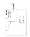
次に、図2を参照して情報処理装置1のより具体的な構成例について説明する。
図2は、情報処理装置1(図1)のプログラム転送装置12をFPGA(Field Programmable Gate Array、プログラム可能な集積回路)で構成した例を示す構成図である。同図において、情報処理装置1は、FPGA12と、プロセッサ14と、フラッシュROM(Flash ROM)16と、フラッシュROM(Flash ROM)17と、DDR・RAM(Double Data Rate RAM、2倍のデータ転送速度を備えたRAM)18とを具備する。FPGA12は、RAM122と、DMA(Direct Memory Access)処理部123と、入出力処理部124と、割込制御部125と、コンフィグレーション(Configulation)制御部126とを具備する。プロセッサ14は、プロセッサ・コア(Processor Core)141と、PCIeコントローラ(PCI Express Controller)142と、フラッシュ・コントローラ(Flash Controller)143と、メモリ・コントローラ(Memory Controller)144と、割込生成部(Programmable Interrupt Controller;PIC)145とを具備する。Next, a more specific configuration example of the information processing apparatus 1 will be described with reference to FIG.
FIG. 2 is a configuration diagram showing an example in which the
また、FPGA12(コンフィグレーション制御部126)とフラッシュROM17と、プロセッサ14(フラッシュ・コントローラ143)とフラッシュROM16と、プロセッサ14(メモリ・コントローラ144)とDDR・RAM18とは、それぞれ専用バスで接続されている。また、プロセッサ14のPCIeコントローラ142と、FPGA12の入出力処理部124とは、PCIeバス(PCI Express BUS)21で接続されている。
また、プロセッサ14において、プロセッサ・コア141と、PCIeコントローラ142と、フラッシュ・コントローラ143と、メモリ・コントローラ144と、割込生成部145とは、内部バス140で接続されている。
同図において、図1の各部に対応して同様の機能を有する部分には同一の符号(1、12、122、14、16、17、18)を付している。Further, the FPGA 12 (configuration controller 126), the
In the
In the figure, the same reference numerals (1, 12, 122, 14, 16, 17, 18) are assigned to parts having similar functions corresponding to the respective parts in FIG.
情報処理装置1は、図1で説明したように、プロセッサが記憶装置からプログラムを読み出して実行する。
フラッシュROM17は、不揮発性メモリであるフラッシュROMで構成される記憶デバイスであり、コンフィグレーション・データを予め(情報処理装置1の電源投入前に)記憶している。このコンフィグレーション・データは、情報処理装置1の電源投入後にFPGA12によって読み出される。また、フラッシュROM17の記憶するコンフィグレーション・データには、プロセッサ14が実行するためのプログラムが含まれる。
フラッシュROM17とFPGA12とは、専用バスで接続されており、この点で、FPGA12はフラッシュROM17に高速にアクセス可能である。As described with reference to FIG. 1, in the information processing apparatus 1, a processor reads a program from a storage device and executes the program.
The
The
DDR・RAM18は、揮発性だがデータ転送速度の速いDDR RAMで構成される記憶デバイスであり、フラッシュROM17よりも高速にアクセス可能である。そして、DDR・RAM18は、FPGA12によってフラッシュROM17から転送されるプログラムを記憶し、プロセッサ14からの読み出しを受けて当該プログラムを出力する。 The DDR /
FPGA12は、図1で説明したのと同様に、フラッシュROM17の記憶する、プロセッサ14が実行するためのプログラムをRAM122に書き込み、さらにDDR・RAM18に転送(転送)する。
RAM122は、図1で説明したのと同様に、揮発性メモリで構成されてフラッシュROM17よりも高速にアクセス可能であり、フラッシュROM17の記憶する、プロセッサ14が実行するためのプログラムをFPGA12によって書き込まれて予め(プロセッサ14の初期化完了前に)記憶している。As described with reference to FIG. 1, the
The
DMA処理部123は、プロセッサ14が実行するためのプログラムの、RAM122からDDR・RAM18への転送処理を制御する。具体的には、DMA処理部123は、転送元アドレスや、転送先アドレスや、転送サイズなどの転送パラメータを予め(プロセッサ14の初期化完了前に)設定されており、当該転送パラメータに従って、RAM122からDDR・RAM18へプログラムをDMA転送する。なお、ここでいうDMA転送は、プロセッサ・コア141を介さずに行うデータ転送であり、DMA処理部123は、入出力処理部124と、PCIeコントローラ142と、メモリ・コントローラ144とを介してDDR・RAM18にアクセスしてプログラムを書き込む。 The
入出力処理部124は、PCIeバス21を介して行われるプロセッサ14(PCIeコントローラ142)との間のデータ入出力を処理する。
割込制御部125は、FPGA12によるDDR・RAM18へのプログラムの書込が終了すると、PCIeバス21を介して割込生成部145にアクセスすることで、プロセッサ・コア141に割込みを発生させる。この割込みは、プログラムの転送を完了したことをプロセッサ・コア141に通知するための割込みであり、当該割り込みを受けたプロセッサ・コア141は、DDR・RAM18の記憶するプログラムの実行を開始する。The input /
When the
コンフィグレーション制御部126は、情報処理装置1の電源が投入されると、FPGA12内部を初期化し、フラッシュROM17からコンフィグレーション・データを読み出す専用回路である。コンフィグレーション制御部126は、フラッシュROM17に専用バスで接続されており、この点で、フラッシュROM17から高速にデータを読み出すことができる。 The
プロセッサ14は、図1で説明したのと同様に、FPGA12によってDDR・RAM18に書き込まれるプログラムを読み出して実行する。
プロセッサ・コア141は、DDR・RAM18の記憶するプログラムを実行して演算(情報処理)を行う演算処理部である。The
The
PCIeコントローラ142は、プロセッサ14の外部の装置との間で行われる、PCIeバス21を介した通信を制御する。また、PCIeコントローラ142は、プロセッサ14の内部バス140のマスターとして動作して、メモリ・コントローラ144を介してDDR・RAM18への読み書きを制御する。これにより、FPGA12は、PCIeバス21を介してPCIeコントローラ142と通信することで、DDR・RAM18にアクセスできる。
また、PCIeコントローラ142は、内部バス140を通じて割込生成部145にアクセス可能であり、これにより、FPGA12は、PCIeコントローラ142を介して割込生成部145にアクセスし、プロセッサ14に対する割込みを発生させることができる。The
Further, the
フラッシュ・コントローラ143は、フラッシュROM16に接続されて当該フラッシュROM16へのアクセスを制御する。ここで、フラッシュROM16は、データ転送速度が遅いが、不揮発性メモリであり、プロセッサ14の電源が切断(OFF)されてもデータを保持(記憶)する。また、プロセッサ14の電源投入後、フラッシュ・コントローラ143は、特に設定を必要とせずにフラッシュROM16の領域の一部にアクセスを行える。この領域に、電源投入直後にプロセッサ14に実行させたいプログラムのコード(プロセッサ14が初期化を行うための初期化コード)を配置することでプロセッサ14を起動させることができる。 The
メモリ・コントローラ144は、DDR・RAM18と専用バスで接続され、当該DDR・RAM18へのアクセスを制御する。ここで、DDR・RAM18は、データ転送速度が速く、高速にリード及びライト可能である。一方、DDR・RAM18は、揮発性メモリであり、情報処理装置1の電源が切断されると、DDR・RAM18の保存するデータが失われる(消去される)。このため情報処理装置1の電源が投入され、メモリ・コントローラ144が初期設定された後に、DDR・RAM18にプログラムを書き込む必要がある。 The
割込生成部145は、プロセッサ・コア141に対する割込みを発生させる。この割込みが発生すると、プロセッサ・コア141は、実行中の処理を中断して、発生した割込みに応じた処理を行う。この割込みを利用して、FPGA12は、プログラムの転送が完了したことをプロセッサ・コア141に通知し、プロセッサ・コア141は、DDR・RAM18の記憶するプログラムの実行を開始する。 The interrupt
フラッシュROM16は、上記のように、データ転送速度が遅いが、不揮発性メモリであり、プロセッサ14の電源が切断(OFF)されてもデータを保持(記憶)する。そして、フラッシュROM16は、上記のように、プロセッサ14を起動させるためのコードを予め記憶している。 As described above, the
なお、コンフィグレーション・データを記憶するフラッシュROM17の配置は、図2に示すFPGA12の外部に限らない。FPGA12が、その内部に不揮発性の記憶装置を有してコンフィグレーション・データを記憶するようにしてもよい。 The arrangement of the
次に、図3を参照して情報処理装置1の動作について説明する。
図3は、情報処理装置1が行う起動処理の手順を示すフローチャートである。情報処理装置1は、電源を投入されると同図の処理を開始する。Next, the operation of the information processing apparatus 1 will be described with reference to FIG.
FIG. 3 is a flowchart illustrating the procedure of the startup process performed by the information processing apparatus 1. The information processing apparatus 1 starts the process shown in FIG.
情報処理装置1の電源を投入されると、FPGA12内のコンフィグレーション制御部126は、フラッシュROM16からコンフィグレーション・データを読み出し、RAM122に転送する(書き込む。ステップS101)。このコンフィグデータには、プロセッサ14の実行するプログラムが含まれる。
この処理を行うコンフィグレーション制御部126は、専用回路にてハードウェア的に実現されている。このため、コンフィグレーション制御部126は、プロセッサ14の負荷を上昇させることなく、高速にコンフィグデータの転送を行うことができる。
コンフィグレーション・データの転送を終了すると、FPGA12は、プロセッサ14からの初期設定完了通知を待つ。When the information processing apparatus 1 is powered on, the
The
When the transfer of the configuration data is completed, the
また、情報処理装置1の電源を投入されると、プロセッサ14は、フラッシュROM16の所定の領域から、プロセッサ・コア141とPCIeコントローラ142とメモリ・コントローラ144との初期設定を行うためのプログラムを読み出して実行する(ステップS102)。
この初期設定により、FPGA12は、PCIeバス21を介してRAM18にアクセス可能となる。
プロセッサ・コア141の初期設定が完了すると、プロセッサ・コア141は、割込生成部145を初期設定してFPGA12からの割込みを受け付けるようにする。割込生成部145の初期設定を完了すると、プロセッサ・コア141は、FPGA12に初期設定完了通知を出力して待機する。When the power of the information processing apparatus 1 is turned on, the
With this initial setting, the
When the initialization of the
FPGA12は、プロセッサ14から出力される初期設定完了通知をトリガとして、プログラムの転送を開始する(ステップS103)。具体的には、FPGA12のDMA処理部123が、予め設定されている転送パラメータ(転送元アドレス、転送先アドレス、転送サイズ)に基づいてDMA転送を開始し、RAM122からDDR・RAM18へと高速にプログラムを転送する。転送を完了すると、FPGA12(割込制御部125)はPCIeバス21を介して割込生成部145にアクセスすることで、プロセッサ・コア141に割込みを発生させる。 The
そして、割込みを受けたプロセッサ・コア141は、DDR・RAM18の記憶するプログラムに処理を移す。すなわち、プロセッサ・コア141は、FPGA12によってDDR・RAM18に書き込まれたプログラムを読み出して実行する(ステップS104)。その後、情報処理装置1は、同図の処理による初期設定を終了し、プロセッサ14によるプログラム実行(通常の情報処理)を行う。 Then, the
なお、プロセッサが実行するためのプログラムを記憶する不揮発性メモリの配置は、図1および図2に示した情報処理装置の内部に限らない。
図4は、外部記憶装置からプログラムを読み出す情報処理装置の概略構成を示す構成図である。
同図において、情報処理装置2は、プログラム転送装置12と、プロセッサ14と、ROM16と、RAM18とを具備する。プログラム転送装置12は、RAM122を具備する。
また、プログラム転送装置12と外部記憶装置37とが、例えば信号ケーブルで接続されている。また、プロセッサ14とROM16と、プロセッサ14とRAM18とは、それぞれデータパス(例えばバス)で接続されている。
同図において、図1の各部に対応して同様の機能を有する部分には、同一の符号(12、122、14、16、18)を付し、説明を省略する。It should be noted that the arrangement of the nonvolatile memory that stores the program to be executed by the processor is not limited to the inside of the information processing apparatus shown in FIGS.
FIG. 4 is a configuration diagram illustrating a schematic configuration of an information processing apparatus that reads a program from an external storage device.
In FIG. 1, the
The
In the same figure, portions having the same functions corresponding to the respective portions in FIG. 1 are denoted by the same reference numerals (12, 122, 14, 16, 18), and description thereof is omitted.
情報処理装置2は、情報処理装置1(図1)と同様、プロセッサが記憶装置からプログラムを読み出して実行する情報処理装置である。情報処理装置2は、情報処理装置1と異なり、記憶デバイス17を具備せず、外部記憶装置37からプログラムを取得する。
外部記憶装置37は、不揮発性メモリを有し、記憶デバイス17(図1)と同様に、情報処理装置2のプロセッサ14が実行するためのプログラムを予め記憶している。The
The
以上の構成において、情報処理装置2のプログラム転送装置12は、情報処理装置2の電源が投入されると、外部記憶装置37の記憶するプログラムを読み出して、RAM122に書き込んでおく。これにより、情報処理装置2は、プログラム転送装置12の具備する高速なRAM122にプログラムを保持するので、RAM18にプログラムを転送する際に、比較的低速な外部記憶装置37から当該プログラムを読み出す必要が無い。このように、情報処理装置2は、情報処理装置1(図1、図2)の場合と同様に、プログラムを高速にDDR・RAM18に転送することができ、情報処理装置2の起動時間を短縮できる。
なお、情報処理装置2の各部は、図2で説明したのと同様に構成することができる。In the above configuration, the
Each unit of the
なお、情報処理装置1(図2。図4に示す情報処理装置1も同様)が、フラッシュROM16を具備しない構成としてもよい。
この場合、情報処理装置1の電源投入後にプロセッサ14が最初に実行するプログラムの保存先を、PCIeバス21で接続されたメモリ領域(例えばRAM122の一部)に設定する。ここで、プロセッサ14が、情報処理装置の電源投入後に、PCIeコントローラ142の設定を必要とせずにRAM122の一部にアクセス可能な構成としておく。Note that the information processing apparatus 1 (FIG. 2; the information processing apparatus 1 shown in FIG. 4 is also the same) may not have the
In this case, a storage destination of a program that is first executed by the
具体的には、FPGA12は、PCIeバス21を介するプロセッサ14からのアクセスを受け付けると、該当するアドレス番地に相当するデータをRAM122から読み出して、プロセッサ14に出力する。これにより、プロセッサ14は、RAM122に対して、プロセッサ14に直接接続されているメモリの領域と同様にアクセスすることができる。 Specifically, when receiving an access from the
以上のように、情報処理装置1の電源投入後にプロセッサ14が最初に実行するプログラムの保存先を、RAM122等とすることで、フラッシュROM16を省略することができる。これにより、情報処理装置1の構成を簡略化することができる。 As described above, the
なお、上述したように、情報処理装置1または2は、コンピュータ等として実現される。すなわち、情報処理装置1または2の全部または一部の機能を実現するためのプログラムをコンピュータ読み取り可能な記録媒体に記録して、この記録媒体に記録されたプログラムをコンピュータシステムに読み込ませ、実行することにより各部の処理を行ってもよい。なお、ここでいう「コンピュータシステム」とは、OSや周辺機器等のハードウェアを含むものとする。
また、「コンピュータシステム」は、WWWシステムを利用している場合であれば、ホームページ提供環境(あるいは表示環境)も含むものとする。
また、「コンピュータ読み取り可能な記録媒体」とは、フレキシブルディスク、光磁気ディスク、ROM、CD−ROM等の可搬媒体、コンピュータシステムに内蔵されるハードディスク等の記憶装置のことをいう。さらに「コンピュータ読み取り可能な記録媒体」とは、インターネット等のネットワークや電話回線等の通信回線を介してプログラムを送信する場合の通信線のように、短時間の間、動的にプログラムを保持するもの、その場合のサーバやクライアントとなるコンピュータシステム内部の揮発性メモリのように、一定時間プログラムを保持しているものも含むものとする。また上記プログラムは、前述した機能の一部を実現するためのものであっても良く、さらに前述した機能をコンピュータシステムにすでに記録されているプログラムとの組み合わせで実現できるものであっても良い。As described above, the
Further, the “computer system” includes a homepage providing environment (or display environment) if a WWW system is used.
The “computer-readable recording medium” refers to a storage device such as a flexible medium, a magneto-optical disk, a portable medium such as a ROM and a CD-ROM, and a hard disk incorporated in a computer system. Furthermore, the “computer-readable recording medium” dynamically holds a program for a short time like a communication line when transmitting a program via a network such as the Internet or a communication line such as a telephone line. In this case, a volatile memory in a computer system serving as a server or a client in that case, and a program that holds a program for a certain period of time are also included. The program may be a program for realizing a part of the functions described above, and may be a program capable of realizing the functions described above in combination with a program already recorded in a computer system.
以上、本発明の実施形態について図面を参照して詳述してきたが、具体的な構成はこの実施形態に限られるものではなく、この発明の要旨を逸脱しない範囲の設計変更等も含まれる。 The embodiment of the present invention has been described in detail with reference to the drawings. However, the specific configuration is not limited to this embodiment, and includes design changes and the like without departing from the gist of the present invention.
1、2 情報処理装置
12 プログラム転送装置(FPGA)
122 RAM
123 DMA処理部
124 入出力処理部
125 割込制御部125
126 コンフィグレーション制御部
14 プロセッサ
140 内部バス
141 プロセッサ・コア
142 PCIeコントローラ
143 フラッシュ・コントローラ
144 メモリ・コントローラ
145 割込生成部
16 ROM(フラッシュROM)
17 記憶デバイス(フラッシュROM)
18 RAM(DDR・RAM)
21 PCIeバス
122 RAM
37 外部記憶装置
1, 2
122 RAM
123
126
17 Storage device (flash ROM)
18 RAM (DDR / RAM)
21
37 External storage
Claims (2)
Translated fromJapanese前記プログラムを記憶する第1記憶装置から前記プログラムを読み出して第2記憶装置に書き込み、前記プロセッサの初期化が完了すると、前記第2記憶装置から前記プログラムを読み出して第3記憶装置に書き込むプログラム転送装置と、
を具備し、
前記プロセッサは、前記第3記憶装置から前記プログラムを読み出して実行することを特徴とする情報処理装置。A processor that reads and executes the program;
Program transfer that reads the program from the first storage device that stores the program and writes it to the second storage device, and when the initialization of the processor is completed, reads the program from the second storage device and writes it to the third storage device Equipment,
Comprising
The information processing apparatus, wherein the processor reads the program from the third storage device and executes the program.
第1記憶装置から前記プロセッサが実行するためのプログラムを読み出して第2記憶装置に書き込む第1転送ステップと、
前記プロセッサの初期化が完了すると、前記第2記憶装置から前記プログラムを読み出して、前記プロセッサが前記プログラムを読み出す際のアクセス先である第3記憶装置に書き込む第2転送ステップと、
を具備することを特徴とするプログラム転送方法。
A program transfer method for an information processing apparatus including a processor,
A first transfer step of reading a program to be executed by the processor from the first storage device and writing it to the second storage device;
When the initialization of the processor is completed, a second transfer step of reading the program from the second storage device and writing to a third storage device that is an access destination when the processor reads the program;
A program transfer method comprising:
Priority Applications (1)
| Application Number | Priority Date | Filing Date | Title |
|---|---|---|---|
| JP2011081500AJP2012216108A (en) | 2011-04-01 | 2011-04-01 | Information processing apparatus and program transfer method |
Applications Claiming Priority (1)
| Application Number | Priority Date | Filing Date | Title |
|---|---|---|---|
| JP2011081500AJP2012216108A (en) | 2011-04-01 | 2011-04-01 | Information processing apparatus and program transfer method |
Publications (1)
| Publication Number | Publication Date |
|---|---|
| JP2012216108Atrue JP2012216108A (en) | 2012-11-08 |
Family
ID=47268812
Family Applications (1)
| Application Number | Title | Priority Date | Filing Date |
|---|---|---|---|
| JP2011081500APendingJP2012216108A (en) | 2011-04-01 | 2011-04-01 | Information processing apparatus and program transfer method |
Country Status (1)
| Country | Link |
|---|---|
| JP (1) | JP2012216108A (en) |
Cited By (2)
| Publication number | Priority date | Publication date | Assignee | Title |
|---|---|---|---|---|
| JP2014149598A (en)* | 2013-01-31 | 2014-08-21 | Fanuc Ltd | Data processor including serial bus that requires initialization at time of use |
| US9996144B2 (en) | 2013-08-08 | 2018-06-12 | Samsung Electronics Co., Ltd. | System on chip for reducing wake-up time, method of operating same, and computer system including same |
Citations (9)
| Publication number | Priority date | Publication date | Assignee | Title |
|---|---|---|---|---|
| JPH02247731A (en)* | 1989-03-20 | 1990-10-03 | Nec Corp | Information processor |
| US20020069354A1 (en)* | 2000-02-03 | 2002-06-06 | Fallon James J. | Systems and methods for accelerated loading of operating systems and application programs |
| JP2005258642A (en)* | 2004-03-10 | 2005-09-22 | Yamaha Corp | Embedded information processor |
| JP2006260092A (en)* | 2005-03-16 | 2006-09-28 | Ricoh Co Ltd | Information processing device or data transfer control device |
| JP2008097105A (en)* | 2006-10-06 | 2008-04-24 | Nec Infrontia Corp | Storage device and activation method |
| JP2009099092A (en)* | 2007-10-19 | 2009-05-07 | Denso Wave Inc | Mobile information terminal |
| US20100070751A1 (en)* | 2008-09-18 | 2010-03-18 | Chee Hoe Chu | Preloader |
| JP2010166267A (en)* | 2009-01-14 | 2010-07-29 | Ricoh Co Ltd | Document utilization system, control method, and program |
| JP2011018241A (en)* | 2009-07-09 | 2011-01-27 | Fujitsu Ltd | Backup device, backup method, and storage system |
- 2011
- 2011-04-01JPJP2011081500Apatent/JP2012216108A/enactivePending
Patent Citations (9)
| Publication number | Priority date | Publication date | Assignee | Title |
|---|---|---|---|---|
| JPH02247731A (en)* | 1989-03-20 | 1990-10-03 | Nec Corp | Information processor |
| US20020069354A1 (en)* | 2000-02-03 | 2002-06-06 | Fallon James J. | Systems and methods for accelerated loading of operating systems and application programs |
| JP2005258642A (en)* | 2004-03-10 | 2005-09-22 | Yamaha Corp | Embedded information processor |
| JP2006260092A (en)* | 2005-03-16 | 2006-09-28 | Ricoh Co Ltd | Information processing device or data transfer control device |
| JP2008097105A (en)* | 2006-10-06 | 2008-04-24 | Nec Infrontia Corp | Storage device and activation method |
| JP2009099092A (en)* | 2007-10-19 | 2009-05-07 | Denso Wave Inc | Mobile information terminal |
| US20100070751A1 (en)* | 2008-09-18 | 2010-03-18 | Chee Hoe Chu | Preloader |
| JP2010166267A (en)* | 2009-01-14 | 2010-07-29 | Ricoh Co Ltd | Document utilization system, control method, and program |
| JP2011018241A (en)* | 2009-07-09 | 2011-01-27 | Fujitsu Ltd | Backup device, backup method, and storage system |
Cited By (7)
| Publication number | Priority date | Publication date | Assignee | Title |
|---|---|---|---|---|
| JP2014149598A (en)* | 2013-01-31 | 2014-08-21 | Fanuc Ltd | Data processor including serial bus that requires initialization at time of use |
| US9223585B2 (en) | 2013-01-31 | 2015-12-29 | Fanuc Corporation | Data processing device with serial bus that needs initialization before use |
| US9996144B2 (en) | 2013-08-08 | 2018-06-12 | Samsung Electronics Co., Ltd. | System on chip for reducing wake-up time, method of operating same, and computer system including same |
| US10642339B2 (en) | 2013-08-08 | 2020-05-05 | Samsung Electronics Co., Ltd. | System on chip for reducing wake-up time, method of operating same, and computer system including same |
| US11372472B2 (en) | 2013-08-08 | 2022-06-28 | Samsung Electronics Co., Ltd. | System on chip for reducing wake-up time, method of operating same, and computer system including same |
| US11635800B2 (en) | 2013-08-08 | 2023-04-25 | Samsung Electronics Co., Ltd. | System on chip for reducing wake-up time, method of operating same, and computer system including same |
| US12248355B2 (en) | 2013-08-08 | 2025-03-11 | Samsung Electronics Co., Ltd. | System on chip for reducing wake-up time, method of operating same, and computer system including same |
Similar Documents
| Publication | Publication Date | Title |
|---|---|---|
| US11042297B2 (en) | Techniques to configure a solid state drive to operate in a storage mode or a memory mode | |
| US9250999B1 (en) | Non-volatile random access memory in computer primary memory | |
| US9477409B2 (en) | Accelerating boot time zeroing of memory based on non-volatile memory (NVM) technology | |
| JP6399916B2 (en) | Information processing apparatus and control method thereof | |
| JP2014059876A5 (en) | Host, nonvolatile memory device, and nonvolatile memory card system | |
| US10162616B2 (en) | System for binary translation version protection | |
| CN103543815A (en) | Information processing apparatus and information processing method | |
| CN106095416B (en) | Jump processing method and device in application program and intelligent terminal | |
| US9575887B2 (en) | Memory device, information-processing device and information-processing method | |
| JP2017033501A (en) | Storage device and control method | |
| TWI507883B (en) | Memory card access device, control method thereof, and memory card access system | |
| CN104122977B (en) | The method and storage system of a kind of data storage | |
| US9934100B2 (en) | Method of controlling memory swap operation and data processing system using same | |
| CN104808953A (en) | Device and method for controlling data storage and mobile terminal | |
| US20220113952A1 (en) | On-demand binary translation state map generation | |
| US9959120B2 (en) | Persistent relocatable reset vector for processor | |
| JP2012216108A (en) | Information processing apparatus and program transfer method | |
| US8806078B2 (en) | Information processing device and program product | |
| JP2007299249A (en) | Nand-type flash memory device and starting method for computing system using it | |
| JP2013182577A (en) | Information processing apparatus, image forming apparatus, and program | |
| US9817672B2 (en) | Information processing apparatus and method for controlling information processing apparatus | |
| JP6312837B2 (en) | Reducing power consumption in computing devices | |
| JP5231496B2 (en) | Information processing apparatus and suspend / resume method thereof | |
| JP6217386B2 (en) | Program generation method for multiprocessor | |
| JP2009093270A (en) | Computer system and its startup method |
Legal Events
| Date | Code | Title | Description |
|---|---|---|---|
| A977 | Report on retrieval | Free format text:JAPANESE INTERMEDIATE CODE: A971007 Effective date:20130424 | |
| A131 | Notification of reasons for refusal | Free format text:JAPANESE INTERMEDIATE CODE: A131 Effective date:20130507 | |
| A521 | Request for written amendment filed | Free format text:JAPANESE INTERMEDIATE CODE: A523 Effective date:20130628 | |
| A02 | Decision of refusal | Free format text:JAPANESE INTERMEDIATE CODE: A02 Effective date:20130806 | |
| A521 | Request for written amendment filed | Free format text:JAPANESE INTERMEDIATE CODE: A523 Effective date:20131106 | |
| A911 | Transfer to examiner for re-examination before appeal (zenchi) | Free format text:JAPANESE INTERMEDIATE CODE: A911 Effective date:20131113 | |
| A912 | Re-examination (zenchi) completed and case transferred to appeal board | Free format text:JAPANESE INTERMEDIATE CODE: A912 Effective date:20131227 |