JP2012213237A - Portable electronic appliance - Google Patents
Portable electronic applianceDownload PDFInfo
- Publication number
- JP2012213237A JP2012213237AJP2012173592AJP2012173592AJP2012213237AJP 2012213237 AJP2012213237 AJP 2012213237AJP 2012173592 AJP2012173592 AJP 2012173592AJP 2012173592 AJP2012173592 AJP 2012173592AJP 2012213237 AJP2012213237 AJP 2012213237A
- Authority
- JP
- Japan
- Prior art keywords
- display device
- tft
- pixel
- substrate
- electrode
- Prior art date
- Legal status (The legal status is an assumption and is not a legal conclusion. Google has not performed a legal analysis and makes no representation as to the accuracy of the status listed.)
- Withdrawn
Links
Images


Classifications
- G—PHYSICS
- G06—COMPUTING OR CALCULATING; COUNTING
- G06F—ELECTRIC DIGITAL DATA PROCESSING
- G06F1/00—Details not covered by groups G06F3/00 - G06F13/00 and G06F21/00
- G06F1/16—Constructional details or arrangements
- G06F1/1613—Constructional details or arrangements for portable computers
- G06F1/1615—Constructional details or arrangements for portable computers with several enclosures having relative motions, each enclosure supporting at least one I/O or computing function
- G06F1/1616—Constructional details or arrangements for portable computers with several enclosures having relative motions, each enclosure supporting at least one I/O or computing function with folding flat displays, e.g. laptop computers or notebooks having a clamshell configuration, with body parts pivoting to an open position around an axis parallel to the plane they define in closed position
- G—PHYSICS
- G02—OPTICS
- G02F—OPTICAL DEVICES OR ARRANGEMENTS FOR THE CONTROL OF LIGHT BY MODIFICATION OF THE OPTICAL PROPERTIES OF THE MEDIA OF THE ELEMENTS INVOLVED THEREIN; NON-LINEAR OPTICS; FREQUENCY-CHANGING OF LIGHT; OPTICAL LOGIC ELEMENTS; OPTICAL ANALOGUE/DIGITAL CONVERTERS
- G02F1/00—Devices or arrangements for the control of the intensity, colour, phase, polarisation or direction of light arriving from an independent light source, e.g. switching, gating or modulating; Non-linear optics
- G02F1/01—Devices or arrangements for the control of the intensity, colour, phase, polarisation or direction of light arriving from an independent light source, e.g. switching, gating or modulating; Non-linear optics for the control of the intensity, phase, polarisation or colour
- G02F1/13—Devices or arrangements for the control of the intensity, colour, phase, polarisation or direction of light arriving from an independent light source, e.g. switching, gating or modulating; Non-linear optics for the control of the intensity, phase, polarisation or colour based on liquid crystals, e.g. single liquid crystal display cells
- G02F1/133—Constructional arrangements; Operation of liquid crystal cells; Circuit arrangements
- G02F1/1333—Constructional arrangements; Manufacturing methods
- G02F1/13338—Input devices, e.g. touch panels
- G—PHYSICS
- G06—COMPUTING OR CALCULATING; COUNTING
- G06F—ELECTRIC DIGITAL DATA PROCESSING
- G06F1/00—Details not covered by groups G06F3/00 - G06F13/00 and G06F21/00
- G06F1/16—Constructional details or arrangements
- G06F1/1613—Constructional details or arrangements for portable computers
- G06F1/1626—Constructional details or arrangements for portable computers with a single-body enclosure integrating a flat display, e.g. Personal Digital Assistants [PDAs]
- G—PHYSICS
- G06—COMPUTING OR CALCULATING; COUNTING
- G06F—ELECTRIC DIGITAL DATA PROCESSING
- G06F1/00—Details not covered by groups G06F3/00 - G06F13/00 and G06F21/00
- G06F1/16—Constructional details or arrangements
- G06F1/1613—Constructional details or arrangements for portable computers
- G06F1/1633—Constructional details or arrangements of portable computers not specific to the type of enclosures covered by groups G06F1/1615 - G06F1/1626
- G06F1/1637—Details related to the display arrangement, including those related to the mounting of the display in the housing
- G06F1/1643—Details related to the display arrangement, including those related to the mounting of the display in the housing the display being associated to a digitizer, e.g. laptops that can be used as penpads
- G—PHYSICS
- G06—COMPUTING OR CALCULATING; COUNTING
- G06F—ELECTRIC DIGITAL DATA PROCESSING
- G06F1/00—Details not covered by groups G06F3/00 - G06F13/00 and G06F21/00
- G06F1/16—Constructional details or arrangements
- G06F1/1613—Constructional details or arrangements for portable computers
- G06F1/1633—Constructional details or arrangements of portable computers not specific to the type of enclosures covered by groups G06F1/1615 - G06F1/1626
- G06F1/1637—Details related to the display arrangement, including those related to the mounting of the display in the housing
- G06F1/1647—Details related to the display arrangement, including those related to the mounting of the display in the housing including at least an additional display
- G—PHYSICS
- G06—COMPUTING OR CALCULATING; COUNTING
- G06F—ELECTRIC DIGITAL DATA PROCESSING
- G06F1/00—Details not covered by groups G06F3/00 - G06F13/00 and G06F21/00
- G06F1/16—Constructional details or arrangements
- G06F1/1613—Constructional details or arrangements for portable computers
- G06F1/1633—Constructional details or arrangements of portable computers not specific to the type of enclosures covered by groups G06F1/1615 - G06F1/1626
- G06F1/1684—Constructional details or arrangements related to integrated I/O peripherals not covered by groups G06F1/1635 - G06F1/1675
- G06F1/1686—Constructional details or arrangements related to integrated I/O peripherals not covered by groups G06F1/1635 - G06F1/1675 the I/O peripheral being an integrated camera
- G—PHYSICS
- G06—COMPUTING OR CALCULATING; COUNTING
- G06F—ELECTRIC DIGITAL DATA PROCESSING
- G06F3/00—Input arrangements for transferring data to be processed into a form capable of being handled by the computer; Output arrangements for transferring data from processing unit to output unit, e.g. interface arrangements
- G06F3/01—Input arrangements or combined input and output arrangements for interaction between user and computer
- G06F3/03—Arrangements for converting the position or the displacement of a member into a coded form
- G06F3/041—Digitisers, e.g. for touch screens or touch pads, characterised by the transducing means
- G06F3/0412—Digitisers structurally integrated in a display
- G—PHYSICS
- G06—COMPUTING OR CALCULATING; COUNTING
- G06F—ELECTRIC DIGITAL DATA PROCESSING
- G06F3/00—Input arrangements for transferring data to be processed into a form capable of being handled by the computer; Output arrangements for transferring data from processing unit to output unit, e.g. interface arrangements
- G06F3/14—Digital output to display device ; Cooperation and interconnection of the display device with other functional units
- G—PHYSICS
- G09—EDUCATION; CRYPTOGRAPHY; DISPLAY; ADVERTISING; SEALS
- G09G—ARRANGEMENTS OR CIRCUITS FOR CONTROL OF INDICATING DEVICES USING STATIC MEANS TO PRESENT VARIABLE INFORMATION
- G09G3/00—Control arrangements or circuits, of interest only in connection with visual indicators other than cathode-ray tubes
- G09G3/20—Control arrangements or circuits, of interest only in connection with visual indicators other than cathode-ray tubes for presentation of an assembly of a number of characters, e.g. a page, by composing the assembly by combination of individual elements arranged in a matrix no fixed position being assigned to or needed to be assigned to the individual characters or partial characters
- G—PHYSICS
- G09—EDUCATION; CRYPTOGRAPHY; DISPLAY; ADVERTISING; SEALS
- G09G—ARRANGEMENTS OR CIRCUITS FOR CONTROL OF INDICATING DEVICES USING STATIC MEANS TO PRESENT VARIABLE INFORMATION
- G09G5/00—Control arrangements or circuits for visual indicators common to cathode-ray tube indicators and other visual indicators
- G09G5/22—Control arrangements or circuits for visual indicators common to cathode-ray tube indicators and other visual indicators characterised by the display of characters or indicia using display control signals derived from coded signals representing the characters or indicia, e.g. with a character-code memory
- H—ELECTRICITY
- H04—ELECTRIC COMMUNICATION TECHNIQUE
- H04M—TELEPHONIC COMMUNICATION
- H04M1/00—Substation equipment, e.g. for use by subscribers
- H04M1/02—Constructional features of telephone sets
- H04M1/0202—Portable telephone sets, e.g. cordless phones, mobile phones or bar type handsets
- H04M1/0206—Portable telephones comprising a plurality of mechanically joined movable body parts, e.g. hinged housings
- H04M1/0208—Portable telephones comprising a plurality of mechanically joined movable body parts, e.g. hinged housings characterized by the relative motions of the body parts
- H04M1/0214—Foldable telephones, i.e. with body parts pivoting to an open position around an axis parallel to the plane they define in closed position
- H—ELECTRICITY
- H04—ELECTRIC COMMUNICATION TECHNIQUE
- H04M—TELEPHONIC COMMUNICATION
- H04M1/00—Substation equipment, e.g. for use by subscribers
- H04M1/02—Constructional features of telephone sets
- H04M1/0202—Portable telephone sets, e.g. cordless phones, mobile phones or bar type handsets
- H04M1/0206—Portable telephones comprising a plurality of mechanically joined movable body parts, e.g. hinged housings
- H04M1/0247—Portable telephones comprising a plurality of mechanically joined movable body parts, e.g. hinged housings comprising more than two body parts
- H—ELECTRICITY
- H04—ELECTRIC COMMUNICATION TECHNIQUE
- H04M—TELEPHONIC COMMUNICATION
- H04M1/00—Substation equipment, e.g. for use by subscribers
- H04M1/72—Mobile telephones; Cordless telephones, i.e. devices for establishing wireless links to base stations without route selection
- H04M1/724—User interfaces specially adapted for cordless or mobile telephones
- H—ELECTRICITY
- H10—SEMICONDUCTOR DEVICES; ELECTRIC SOLID-STATE DEVICES NOT OTHERWISE PROVIDED FOR
- H10K—ORGANIC ELECTRIC SOLID-STATE DEVICES
- H10K59/00—Integrated devices, or assemblies of multiple devices, comprising at least one organic light-emitting element covered by group H10K50/00
- H10K59/40—OLEDs integrated with touch screens
- H—ELECTRICITY
- H10—SEMICONDUCTOR DEVICES; ELECTRIC SOLID-STATE DEVICES NOT OTHERWISE PROVIDED FOR
- H10K—ORGANIC ELECTRIC SOLID-STATE DEVICES
- H10K59/00—Integrated devices, or assemblies of multiple devices, comprising at least one organic light-emitting element covered by group H10K50/00
- H10K59/60—OLEDs integrated with inorganic light-sensitive elements, e.g. with inorganic solar cells or inorganic photodiodes
- H10K59/65—OLEDs integrated with inorganic image sensors
- G—PHYSICS
- G02—OPTICS
- G02F—OPTICAL DEVICES OR ARRANGEMENTS FOR THE CONTROL OF LIGHT BY MODIFICATION OF THE OPTICAL PROPERTIES OF THE MEDIA OF THE ELEMENTS INVOLVED THEREIN; NON-LINEAR OPTICS; FREQUENCY-CHANGING OF LIGHT; OPTICAL LOGIC ELEMENTS; OPTICAL ANALOGUE/DIGITAL CONVERTERS
- G02F2203/00—Function characteristic
- G02F2203/02—Function characteristic reflective
- G—PHYSICS
- G09—EDUCATION; CRYPTOGRAPHY; DISPLAY; ADVERTISING; SEALS
- G09G—ARRANGEMENTS OR CIRCUITS FOR CONTROL OF INDICATING DEVICES USING STATIC MEANS TO PRESENT VARIABLE INFORMATION
- G09G2300/00—Aspects of the constitution of display devices
- G09G2300/08—Active matrix structure, i.e. with use of active elements, inclusive of non-linear two terminal elements, in the pixels together with light emitting or modulating elements
- G09G2300/0809—Several active elements per pixel in active matrix panels
- G09G2300/0842—Several active elements per pixel in active matrix panels forming a memory circuit, e.g. a dynamic memory with one capacitor
- G—PHYSICS
- G09—EDUCATION; CRYPTOGRAPHY; DISPLAY; ADVERTISING; SEALS
- G09G—ARRANGEMENTS OR CIRCUITS FOR CONTROL OF INDICATING DEVICES USING STATIC MEANS TO PRESENT VARIABLE INFORMATION
- G09G2340/00—Aspects of display data processing
- G09G2340/04—Changes in size, position or resolution of an image
- G09G2340/0407—Resolution change, inclusive of the use of different resolutions for different screen areas
- H—ELECTRICITY
- H04—ELECTRIC COMMUNICATION TECHNIQUE
- H04M—TELEPHONIC COMMUNICATION
- H04M2250/00—Details of telephonic subscriber devices
- H04M2250/16—Details of telephonic subscriber devices including more than one display unit
- H—ELECTRICITY
- H04—ELECTRIC COMMUNICATION TECHNIQUE
- H04M—TELEPHONIC COMMUNICATION
- H04M2250/00—Details of telephonic subscriber devices
- H04M2250/22—Details of telephonic subscriber devices including a touch pad, a touch sensor or a touch detector
- H—ELECTRICITY
- H10—SEMICONDUCTOR DEVICES; ELECTRIC SOLID-STATE DEVICES NOT OTHERWISE PROVIDED FOR
- H10K—ORGANIC ELECTRIC SOLID-STATE DEVICES
- H10K59/00—Integrated devices, or assemblies of multiple devices, comprising at least one organic light-emitting element covered by group H10K50/00
- H10K59/10—OLED displays
- H10K59/12—Active-matrix OLED [AMOLED] displays
Landscapes
- Engineering & Computer Science (AREA)
- Theoretical Computer Science (AREA)
- Physics & Mathematics (AREA)
- Computer Hardware Design (AREA)
- General Physics & Mathematics (AREA)
- Human Computer Interaction (AREA)
- General Engineering & Computer Science (AREA)
- Chemical & Material Sciences (AREA)
- Signal Processing (AREA)
- Nonlinear Science (AREA)
- Mathematical Physics (AREA)
- Inorganic Chemistry (AREA)
- Optics & Photonics (AREA)
- Crystallography & Structural Chemistry (AREA)
- Life Sciences & Earth Sciences (AREA)
- Sustainable Development (AREA)
- Computer Networks & Wireless Communication (AREA)
- Devices For Indicating Variable Information By Combining Individual Elements (AREA)
- Control Of Indicators Other Than Cathode Ray Tubes (AREA)
- Telephone Function (AREA)
- Electroluminescent Light Sources (AREA)
- Control Of El Displays (AREA)
- Liquid Crystal (AREA)
- Input From Keyboards Or The Like (AREA)
- Telephone Set Structure (AREA)
- Liquid Crystal Display Device Control (AREA)
- Position Input By Displaying (AREA)
Abstract
Description
Translated fromJapanese 本発明は薄膜トランジスタ(以下、TFTという)で構成された回路を有する表示部を
備えた携帯型の電子機器に関する。例えば、液晶表示パネルに代表される表示装置を表示
部として搭載した携帯型の電子機器に関する。The present invention relates to a portable electronic device provided with a display portion having a circuit formed of a thin film transistor (hereinafter referred to as TFT). For example, the present invention relates to a portable electronic device in which a display device typified by a liquid crystal display panel is mounted as a display unit.
なお、本明細書中において携帯型の電子機器とは、携帯型の情報処理装置全般を指し、
携帯電話、携帯テレビ電話、あるいは携帯型コンピュータ等である。In this specification, the portable electronic device refers to all portable information processing apparatuses,
A mobile phone, a mobile videophone, a portable computer, or the like.
従来、携帯電話においては、表示部として通常では液晶表示装置が1個使用されている
。また、前記表示部は、小型化の要請上、画面の大きさが限られていた。Conventionally, in a mobile phone, one liquid crystal display device is usually used as a display unit. Further, the display unit has a limited screen size due to a demand for miniaturization.
また、近年では通信技術の発達により、携帯電話を使って電子メールの送受信やインタ
ーネットのホームページへのアクセスができるようになった。In recent years, with the development of communication technology, it has become possible to send and receive e-mails and access Internet homepages using mobile phones.
近年になって、携帯電話で電子メールの送受信ができるようになったものの、テキスト
形式の文字しか送受信できず、例えばパソコン等から画像データを添付したメッセージを
受信しても、携帯電話の表示部に画像データを表示することはできなかった。In recent years, it has become possible to send and receive e-mails on mobile phones, but only text characters can be sent and received. For example, even if a message with image data attached is received from a personal computer or the like, the display unit of the mobile phone The image data could not be displayed on the screen.
また、インターネットのホームページにアクセスしても携帯電話の表示部にホームペー
ジ上の画像データを表示することはできなかった。Further, even when accessing the Internet home page, the image data on the home page cannot be displayed on the display unit of the mobile phone.
従来の携帯電話の表示部には文字の出力、もしくは簡単な映像の出力で十分であったた
め、高精細である必要性はあまりなく、フルカラーである必要性もなかった。Since the output of characters or simple video output was sufficient for the display portion of a conventional mobile phone, there was not much need for high definition and there was no need for full color.
しかし、近年になって携帯電話で電子メールの送受信ができるようになり、高精細、且
つフルカラーである必要性が高まってきた。様々な携帯電話のなかには、画像データを表
示できるものも販売されているが、白黒などの2色表示であるものが多く、フルカラーの
ものもあるが画質が低く見づらいものであった。However, in recent years, it has become possible to send and receive e-mails with mobile phones, and the need for high definition and full color has increased. Among various mobile phones, those that can display image data are on the market, but many are two-color displays such as black and white, and some are full color, but the image quality is low and difficult to see.
また、表示部に画像データを表示させると文字を表示させることはできず、画像と文字
とを同時に表示することはできていない。Further, when image data is displayed on the display unit, characters cannot be displayed, and images and characters cannot be displayed simultaneously.
本明細書で開示する発明の構成は、 映像を表示する第1の表示装置と、 タッチ入力操
作部を備えた第2の表示装置とを縦方向または横方向に並べて装着した携帯型の電子機器
である。なお、図2に示した電子機器は、縦方向に並べて装着したものである。The configuration of the invention disclosed in this specification is a portable electronic device in which a first display device that displays video and a second display device that includes a touch input operation unit are mounted side by side in the vertical direction or the horizontal direction. It is. Note that the electronic devices shown in FIG. 2 are mounted side by side in the vertical direction.
また、他の発明の構成は、 映像を表示する第1の表示装置を備えた蓋部材と、 タッ
チ入力操作部を備えた第2の表示装置とを開閉自在に装着した携帯型の電子機器である。
なお、図1に示した電子機器は、開閉自在に装着したものである。According to another aspect of the invention, there is provided a portable electronic device in which a lid member provided with a first display device for displaying an image and a second display device provided with a touch input operation unit are detachably mounted. is there.
Note that the electronic device shown in FIG. 1 is mounted so as to be freely opened and closed.
また、図3に示したような形態、即ち、前記蓋部材と前記第2の表示装置との間に第3
の表示装置を設けてもよい。さらに、第4、第5の表示装置を設けて画面数を増加させ、
表示領域を拡大してもよい。また、前記3の表示装置に撮像素子あるいはセンサを備えて
もよい。また、前記第3の表示装置に使用者を識別するシステムを備えてもよい。In addition, a configuration as shown in FIG. 3, that is, a third space between the lid member and the second display device.
The display device may be provided. Furthermore, the fourth and fifth display devices are provided to increase the number of screens,
The display area may be enlarged. Further, the display device of 3 may be provided with an image sensor or a sensor. Further, the third display device may include a system for identifying a user.
また、上記各構成において、前記第2の表示装置だけでなく、前記第1の表示装置にも
タッチ入力操作部を備えてよい。In each of the above configurations, not only the second display device but also the first display device may include a touch input operation unit.
また、上記各構成において、前記第2の表示装置は、高精細な画面は必要とされず、文
字または記号を表示することを専門に表示するものであってもよい。このようにすれば、
第1の表示装置を第2の表示装置より高精細なものとすることでコスト上昇を抑える。例
えば、第1の表示装置にポリシリコンを半導体層とするTFTを用い、第2の表示装置に
アモルファスシリコンを半導体層とするTFTを用いた電子機器とすればよい。In each of the above configurations, the second display device does not need a high-definition screen and may specially display characters or symbols. In this way,
An increase in cost is suppressed by making the first display device more precise than the second display device. For example, an electronic device using a TFT with polysilicon as a semiconductor layer for the first display device and a TFT with amorphous silicon as a semiconductor layer for the second display device may be used.
また、上記各構成において、前記第1の表示装置または前記第2の表示装置に撮像素子
あるいはセンサを取り付けてもよいし、各画素内に備えてもよい。In each of the above configurations, an imaging element or a sensor may be attached to the first display device or the second display device, or may be provided in each pixel.
また、上記各構成において、前記第1の表示装置または前記第2の表示装置に使用者を
識別するシステムを備えてもよい。In each of the above configurations, a system for identifying a user may be provided in the first display device or the second display device.
また、上記各構成において、前記第1の表示装置、前記第2の表示装置、または前記第
3の表示装置は適宜、液晶表示装置またはEL表示装置とすればよい。
また、前記第1の表示装置、前記第2の表示装置、または前記第3の表示装置として、他
の表示装置、例えば、エレクトロケミカルディスプレイ、フィールドエミッションディス
プレイ、プラズマディスプレイ、DMD等を用いることが可能である。In each of the above structures, the first display device, the second display device, or the third display device may be a liquid crystal display device or an EL display device as appropriate.
Further, as the first display device, the second display device, or the third display device, other display devices such as an electrochemical display, a field emission display, a plasma display, and a DMD can be used. It is.
なお、本明細書中において、EL表示装置とは、有機発光素子(OLED:Organic Li
ght Emitting Device)が形成された発光装置を指している。Note that in this specification, an EL display device is an organic light-emitting element (OLED: Organic Lithium).
ght Emitting Device).
また、他の発明の構成は、映像を表示するEL表示装置を備えた蓋部材と、反射型表示
装置とを開閉自在に装着し、前記EL表示装置の発光による光を照射させて前記反射型表
示装置を表示する携帯型の電子機器である。According to another aspect of the invention, a lid member having an EL display device for displaying an image and a reflective display device are mounted so as to be openable and closable, and light emitted from the EL display device is irradiated to emit the reflective type. It is a portable electronic device that displays a display device.
上記構成においては、前記反射型表示装置にタッチ入力操作部を備えてもよい。 In the above configuration, the reflective display device may include a touch input operation unit.
なお、上記反射型表示装置とは、反射型の液晶表示装置やDMD(Degital M
icromirror Device)などで代表される光の反射を利用して表示を行う
デバイスを指している。また、本明細書中において、反射型の液晶表示装置とは、画素電
極を透光性を有する導電膜と、反射性を有する金属材料との両方で形成した半透過型の液
晶表示装置も含む。The reflective display device is a reflective liquid crystal display device or DMD (Digital M).
It refers to a device that performs display using reflection of light typified by a “mirror device”. In this specification, the reflective liquid crystal display device also includes a transflective liquid crystal display device in which a pixel electrode is formed using both a light-transmitting conductive film and a reflective metal material. .
また、他の発明の構成は、EL表示装置と、液晶表示装置とを縦方向または横方向に並
べて装着した携帯型の電子機器である。Another embodiment of the invention is a portable electronic device in which an EL display device and a liquid crystal display device are mounted side by side in the vertical direction or the horizontal direction.
上記構成において、前記EL表示装置は、文字または記号を表示することを特徴として
いる。また、上記構成において、前記EL表示装置は、撮像素子を備えたことを特徴とし
ている。In the above structure, the EL display device displays characters or symbols. In the above structure, the EL display device includes an imaging element.
また、上記各構成において、前記携帯型の電子機器は、通信機能を備えた電子機器であ
り、代表的には携帯電話、携帯情報端末である。In each of the above structures, the portable electronic device is an electronic device having a communication function, and is typically a mobile phone or a portable information terminal.
従来、操作ボタンであった部分を表示画面とすることで、電子機器の外形寸法を変える
ことなく表示領域を大きくすることができ、一度に多くの情報を表示できる。Conventionally, by using a portion that was an operation button as a display screen, the display area can be enlarged without changing the external dimensions of the electronic device, and a large amount of information can be displayed at a time.
また、本発明により携帯電話で高精細な画像と文字の両方を同時に見ることが容易にでき
る。In addition, according to the present invention, it is possible to easily view both high-definition images and characters simultaneously on a mobile phone.
本発明の実施形態について、以下に説明する。 Embodiments of the present invention will be described below.
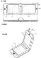
図1(A)〜(C)に本発明の携帯型の電子機器の一例である携帯電話の上面図、側面
図、および斜視図を示す。1A to 1C are a top view, a side view, and a perspective view of a mobile phone which is an example of the portable electronic device of the present invention.
図1に示した携帯電話は、主に画像をカラー表示する高画質な第1の表示装置101と
、主に文字や記号を表示する第2の表示装置102とを備えている。The mobile phone shown in FIG. 1 includes a high-quality
また、第1の表示装置または第2の表示装置のうち、少なくとも一方はタッチ入力操作
部を備えている。また、タッチ入力操作部を備えた画面は操作スイッチの役割をも果たし
ている。図1では第1の表示装置及び第2の表示装置とはモジュールを指している。At least one of the first display device and the second display device includes a touch input operation unit. The screen provided with the touch input operation unit also serves as an operation switch. In FIG. 1, the first display device and the second display device indicate modules.
図1に示した電子機器は、映像(デジタル静止画像等)を表示する第1の表示装置を備
えた蓋部材と、タッチ入力操作部を備えた第2の表示装置(文字や記号等を表示する)と
を開閉自在に装着した携帯型の電子機器である。図1に示す携帯電話は折りたたみ式にな
っている。いずれの形、例えば図2の形態でも本発明は実施できるが表示部を保護するこ
とができることから図1に示すような折りたたみ式のほうが望ましい。The electronic device shown in FIG. 1 has a lid member having a first display device that displays video (digital still image or the like) and a second display device having a touch input operation unit (displays characters, symbols, and the like). Mobile electronic device that can be freely opened and closed. The mobile phone shown in FIG. 1 is foldable. Although the present invention can be carried out in any form, for example, in the form of FIG. 2, the foldable form as shown in FIG.
また、図1に示した折りたたみ式であれば、第1の表示装置としてEL表示装置を用い、
第2の表示装置を反射型の液晶表示装置とした場合、軽く折りたたんで第1の表示装置の
表示画面を第2の表示装置に近づければ、暗いところでも第1の表示装置のEL素子から
発光される光を利用して第2の表示装置の画面を視認することができる。In the case of the folding type shown in FIG. 1, an EL display device is used as the first display device.
When the second display device is a reflective liquid crystal display device, if the display screen of the first display device is brought close to the second display device by folding it lightly, the EL element of the first display device can be used even in a dark place. The screen of the second display device can be visually recognized using the emitted light.
また、図1に示した電子機器は、数個の操作ボタン103、音声出力部104、音声入
力部105、アンテナ106も備えている。The electronic device illustrated in FIG. 1 also includes
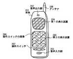
また、図2に示すように、映像を表示する第1の表示装置204と、タッチ入力操作部
を備えた第2の表示装置205とを縦方向に並べて装着した携帯型の電子機器としてもよ
い。図2では第1の表示装置及び第2の表示装置とはモジュールを指している。Further, as shown in FIG. 2, a portable electronic device in which a
また、図4に示すように、第3の表示装置403を挟むように第1の表示装置401と
第2の表示装置402とで開閉自在に装着した携帯型の電子機器としてもよい。図4では
第1の表示装置、第2の表示装置、及び第3の表示装置とはモジュールを指している。Alternatively, as illustrated in FIG. 4, a portable electronic device in which the
また、図5に示すように、CCD撮像素子等の画像入力部507を搭載した携帯型の電
子機器としてもよい。図5では第1の表示装置及び第2の表示装置とはモジュールと該モ
ジュールと接続された他の素子、配線、およびこれらを覆うカバーとを含む装置を指して
いる。このように本明細書では、モジュール及びその他の部材を含む全体を表示装置と呼
ぶこともあれば、液晶モジュールやELモジュール自体を表示装置と呼ぶこともある。Further, as shown in FIG. 5, a portable electronic device equipped with an
また、第1の表示装置、第2の表示装置、または第3の表示装置に使用者の認証を行う
センサを備えてもよい。使用者の認証は生体情報(代表的には指紋、掌紋、声紋等)を利
用すればよい。Moreover, you may provide the sensor which authenticates a user in a 1st display apparatus, a 2nd display apparatus, or a 3rd display apparatus. For user authentication, biometric information (typically fingerprints, palm prints, voice prints, etc.) may be used.
なお、第1の表示装置、第2の表示装置、または第3の表示装置としては、液晶表示装
置あるいはEL表示装置を用いることが可能である。Note that a liquid crystal display device or an EL display device can be used as the first display device, the second display device, or the third display device.
以上の構成でなる本発明について、以下に示す実施例でもってさらに詳細な説明を行う
こととする。The present invention having the above-described configuration will be described in more detail with the following examples.
本実施例では、図1(A)〜(C)に示した折りたたみ式の携帯型の電子機器について
説明する。図1(A)は上面図であり、図1(B)は側面図であり、図1(C)は斜視図
である。In this embodiment, a folding portable electronic device shown in FIGS. 1A to 1C will be described. 1A is a top view, FIG. 1B is a side view, and FIG. 1C is a perspective view.
図1(A)〜(C)中において、101は第1の表示装置、102は第2の表示装置、
103は操作スイッチ、104は音声出力部、105は音声入力部、106はアンテナで
ある。1A to 1C, 101 is a first display device, 102 is a second display device,
本実施例では第1の表示装置101に高画質な表示が可能なEL表示装置、第2の表示
装置102に液晶表示装置を用いた。また、第2の表示装置にはタッチパネル方式を採用
している。第1の表示装置101にEL表示装置を使用することによって、液晶表示装置
のように受信したデジタル信号をアナログ信号に変換する必要なくデジタル画像を表示で
きるため好ましい。なお、タッチパネルは第2の表示装置、即ち液晶表示装置に圧電素子
を組み込むことによって実現することができる。In this embodiment, an EL display device capable of high-quality display is used for the
図3(A)は、第2の表示装置102における初期画面の例である。第2の表示装置1
02には、電話ボタン、電子メールボタン、インターネットボタン、電話帳ボタン、メモ
リーボタンなどが表示される。FIG. 3A is an example of an initial screen in the
In 02, a telephone button, an e-mail button, an Internet button, a telephone directory button, a memory button, and the like are displayed.
例えば、第2の表示装置102に映し出された電話ボタンを押すと、画面が切り替わり
、図3(B)のようなダイヤルボタンが表示される。表示されたこれらのダイヤルボタン
を使って通話したい相手の電話番号を入力することで相手と通話できる。電話番号を入力
するとき、入力した番号は第2の表示装置または第1の表示装置に表示されることが望ま
しい。For example, when a telephone button displayed on the
また、第2の表示装置102に映し出された電話帳ボタンを押して、予め入力しておい
た相手の電話番号を表示させて通話することもできる。そのとき電話帳を表示する画面は
図1に示す第1の表示装置であっても良い。It is also possible to make a call by pressing the telephone directory button displayed on the
また、第2の表示装置102に映し出された電子メールボタンまたはインターネットボ
タンを押すと、画面が切り替わり、図3(C)のようなキーボードボタンが表示される。
表示されたこれらのキーボードボタンを使って、電子メールのアドレスや、ホームページ
のURL(Uniform Resource Locator)を入力することができる。表示された各種入力キ
ーに対応する部分をタッチすることにより、その表示内容のデータ入力が可能になる。な
お、キーボードボタンは適宜、大文字、小文字、数字を入力することができる画面に切り
替えることができ、日本語入力も可能である。このとき、入力した番号は第2の表示装置
または第1の表示装置に表示されることが望ましい。Further, when an e-mail button or an Internet button displayed on the
Using these displayed keyboard buttons, an e-mail address and a homepage URL (Uniform Resource Locator) can be input. By touching a portion corresponding to the displayed various input keys, data input of the display contents becomes possible. In addition, the keyboard button can be switched to a screen for inputting uppercase letters, lowercase letters, and numbers as appropriate, and Japanese input is also possible. At this time, the input number is preferably displayed on the second display device or the first display device.
また、第2の表示装置102に映し出された電話帳ボタンを押して、予め入力しておい
た電子メールアドレスを出力し、電子メールの送信を行ったり、ホームページのURLを
出力し、ホームページを参照することもできる。そのとき電話帳を表示する画面は図1に
示す第1の表示装置101であっても良い。In addition, the telephone directory button displayed on the
本実施例の携帯電話で写真や絵などの画像が添付された電子メールを受信した場合、画
像は高画質な表示が可能な第1の表示装置101に表示し、テキスト形式の文字や記号は
第2の表示装置102に表示可能であることを特徴としている。また、画像を第1の表示
装置で表示したまま、第2の表示装置に表示された画面だけをスクロールさせて文章を読
みとることが可能である。When an e-mail attached with an image such as a picture or a picture is received by the mobile phone of the present embodiment, the image is displayed on the
また、画像が添付された電子メールだけでなく、音声が添付された電子メールも受信す
ることが可能である。It is also possible to receive not only an e-mail with an image attached but also an e-mail with an audio attached.
例えば、本実施例の携帯電話でホームページを見る場合、公開されている写真や絵など
の画像は高画質な表示が可能な第1の表示装置101に表示し、その画像の説明やメッセ
ージなどの文字は第2の表示装置102に表示する。For example, when viewing a homepage on the mobile phone of this embodiment, images such as pictures and pictures that are publicly displayed are displayed on the
本発明により携帯電話で画像と文字の両方を同時に見ることが容易にできる。According to the present invention, it is possible to easily view both images and characters simultaneously on a mobile phone.
また、本実施例のように第1の表示装置としてEL表示装置を用い、第2の表示装置を反
射型の液晶表示装置とした場合、軽く折りたたんで第1の表示装置の表示画面を第2の表
示装置に近づければ暗いところでも第1の表示装置のEL素子から発光される光を利用し
て第2の表示装置の画面を視認することができる。Further, when an EL display device is used as the first display device as in the present embodiment and the second display device is a reflective liquid crystal display device, the display screen of the first display device is displayed in the second display by folding it lightly. The screen of the second display device can be visually recognized by using the light emitted from the EL element of the first display device even in a dark place if it is close to the display device.
なお、本実施例では、第1の表示装置としてEL表示装置を用い、第2の表示装置とし
て液晶表示装置を用いた例を示したが、特に限定されず、第1の表示装置101または第
2の表示装置102として、液晶表示装置あるいはEL表示装置を適宜用いることが可能
である。Note that although an example in which an EL display device is used as the first display device and a liquid crystal display device is used as the second display device is described in this embodiment, there is no particular limitation, and the
実施例1では、折りたたみ式の携帯型の電子機器について説明したが、本実施例では、
図2に示すように、映像を表示する第1の表示装置204と、タッチ入力操作部を備えた
第2の表示装置205とを縦方向に並べて装着した携帯型の電子機器について説明する。In the first embodiment, the folding portable electronic device has been described. However, in this embodiment,
As shown in FIG. 2, a portable electronic device in which a
なお、本実施例は、実施例1とは本体の形態が異なるだけで、その他は同一であるため
、詳細な説明は省略する。The present embodiment is different from the first embodiment only in the form of the main body, and the others are the same, and thus detailed description thereof is omitted.
図2中において、201は本体、202は音声出力部、203は音声入力部、206は
、第2の表示装置205に表示された操作スイッチの画像206、207は操作スイッチ
、208はアンテナである。In FIG. 2, 201 is a main body, 202 is an audio output unit, 203 is an audio input unit, 206 is an operation switch image displayed on the
なお、第1の表示装置204または第2の表示装置205としては、液晶表示装置ある
いはEL表示装置を用いることが可能である。Note that a liquid crystal display device or an EL display device can be used as the
本実施例では、2つ以上の表示装置を備えた携帯型の電子機器の例について説明する。
図4(A)は側面図であり、図4(B)は斜視図である。なお、本実施例は、実施例1と
は表示装置の数が異なるだけで、その他は同一であるため、詳細な説明は省略する。In this embodiment, an example of a portable electronic device including two or more display devices will be described.
4A is a side view, and FIG. 4B is a perspective view. Note that this embodiment is the same as the first embodiment except for the number of display devices, and the others are the same.
図4(A)及び図4(B)に示すように、本実施例の電子機器は、第3の表示装置40
3を挟むように第1の表示装置401と第2の表示装置402とで開閉自在に装着した携
帯型の電子機器である。図4に示す電子機器は、書籍のようになっており、ページをめく
るように第3の表示装置を動かすことができる。As shown in FIG. 4A and FIG. 4B, the electronic apparatus of the present embodiment includes a third display device 40.
3 is a portable electronic device that can be freely opened and closed by a
第3の表示装置403を透過型の表示装置とした場合、第1の表示装置401からの光
、或いは第2の表示装置402からの光をバックライトとして利用してよりよい表示を行
うことができる。また、第3の表示装置を反射型の表示装置とした場合、外光だけでなく
、第1の表示装置401からの光、或いは第2の表示装置402からの光を利用してより
よい表示を行うことができる。In the case where the
図4(B)中において、404は操作スイッチ、405は音声出力部、406は音声入
力部、407はアンテナである。In FIG. 4B, 404 is an operation switch, 405 is an audio output unit, 406 is an audio input unit, and 407 is an antenna.
また、第1の表示装置、第2の表示装置、または第3の表示装置に使用者の認証を行う
センサを備えてもよい。使用者の認証は生体情報(代表的には指紋、掌紋、声紋等)を利
用すればよい。Moreover, you may provide the sensor which authenticates a user in a 1st display apparatus, a 2nd display apparatus, or a 3rd display apparatus. For user authentication, biometric information (typically fingerprints, palm prints, voice prints, etc.) may be used.
また、第1の表示装置、第2の表示装置、または第3の表示装置にタッチ入力操作部や
撮像素子を備えてもよい。Further, the first display device, the second display device, or the third display device may be provided with a touch input operation unit or an image sensor.
なお、第1の表示装置、第2の表示装置、または第3の表示装置としては、液晶表示装
置あるいはEL表示装置を用いることが可能である。Note that a liquid crystal display device or an EL display device can be used as the first display device, the second display device, or the third display device.
本実施例では、撮像素子を備えた携帯型の電子機器の例について説明する。図5は斜視図
である。In this embodiment, an example of a portable electronic device including an image sensor will be described. FIG. 5 is a perspective view.
なお、本実施例は、撮像素子を備えた点以外は実施例1と同一であるため、詳細な説明
は省略する。Since the present embodiment is the same as the first embodiment except that an image sensor is provided, detailed description thereof is omitted.
図5中において、501は第1の表示装置、502は第2の表示装置、503は操作スイ
ッチ、504は音声出力部、505は音声入力部、506はアンテナ、507は画像入力
部である。In FIG. 5, 501 is a first display device, 502 is a second display device, 503 is an operation switch, 504 is an audio output unit, 505 is an audio input unit, 506 is an antenna, and 507 is an image input unit.
本実施例では画像入力部としてCCD撮像素子を用い、使用者の自分の顔画像を相手に
送信し、かつ相手の顔画像を受信しながら通常の会話と同じように通話を行うことができ
る。In this embodiment, a CCD image sensor is used as the image input unit, and the user's own face image can be transmitted to the other party, and a call can be made in the same manner as a normal conversation while receiving the other party's face image.
また、本実施例は、実施例1乃至3のいずれか一と自由に組み合わせることが可能であ
る。In addition, this embodiment can be freely combined with any one of Embodiments 1 to 3.
本実施例では、実施例1〜実施例4に示した第1の表示装置または第2の表示装置とな
る液晶表示装置の一例を示す。In this embodiment, an example of a liquid crystal display device which is the first display device or the second display device shown in Embodiments 1 to 4 will be described.
基板上に画素部とそれを駆動する駆動回路を有した基板(アクティブマトリクス基板と
呼ばれる)の例(但し液晶材料封止前の状態)を図6に示す。FIG. 6 shows an example of a substrate (called an active matrix substrate) having a pixel portion and a driving circuit for driving the pixel portion on the substrate (a state before sealing with a liquid crystal material).
なお、駆動回路には基本単位となるCMOS回路を示し、画素部には一つの画素を示す
。Note that a CMOS circuit serving as a basic unit is shown in the driver circuit, and one pixel is shown in the pixel portion.
図6において、ガラスやプラスチックからなる基板上にはnチャネル型TFT605、
606とpチャネル型TFT603、604からなる駆動回路601、nチャネル型TF
Tからなる画素TFT607および保持容量608からなる画素部602とが形成されて
いる。また、本実施例では、TFTはすべてトップゲート型TFTで形成されている。In FIG. 6, an n-channel TFT 605 is formed on a substrate made of glass or plastic.
606 and p-channel TFTs 603 and 604, a driving
A pixel TFT 607 made of T and a pixel portion 602 made of a storage capacitor 608 are formed. In this embodiment, all TFTs are formed by top gate type TFTs.
また、画素TFT607はソース領域およびドレイン領域の間に二つのチャネル形成領域
を有した構造(ダブルゲート構造)となっているが、本実施例はダブルゲート構造に限定
されることなく、チャネル形成領域が一つ形成されるシングルゲート構造もしくは三つ形
成されるトリプルゲート構造であっても良い。The pixel TFT 607 has a structure (double gate structure) having two channel formation regions between the source region and the drain region. However, the present embodiment is not limited to the double gate structure, and the channel formation region A single gate structure in which one is formed or a triple gate structure in which three are formed may be used.
また、本実施例では、画素TFTのドレイン領域と接続する画素電極を反射電極とした
。その画素電極610の材料としては、AlまたはAgを主成分とする膜、またはそれら
の積層膜等の反射性の優れた材料を用いることが望ましい。また、画素電極を形成した後
、公知のサンドブラスト法やエッチング法等の工程を追加して表面を凹凸化させて、鏡面
反射を防ぎ、反射光を散乱させることによって白色度を増加させることが好ましい。In this embodiment, the pixel electrode connected to the drain region of the pixel TFT is a reflective electrode. As a material of the pixel electrode 610, it is desirable to use a material having excellent reflectivity such as a film containing Al or Ag as a main component or a laminated film thereof. Further, after forming the pixel electrode, it is preferable to increase the whiteness by adding a step such as a known sandblasting method or an etching method to make the surface uneven, thereby preventing specular reflection and scattering the reflected light. .
なお、本実施例では画素電極を反射電極とした反射型の液晶表示装置の例を示したが、
反射電極に代えて画素電極として透明導電膜を用いた透過型の液晶表示装置を用いてもよ
い。In the present embodiment, an example of a reflective liquid crystal display device having a pixel electrode as a reflective electrode is shown.
Instead of the reflective electrode, a transmissive liquid crystal display device using a transparent conductive film as a pixel electrode may be used.
図6の状態を得た後、画素電極上に配向膜を形成しラビング処理を行う。なお、本実施
例では配向膜を形成する前に、アクリル樹脂膜等の有機樹脂膜をパターニングすることに
よって基板間隔を保持するための柱状のスペーサを所望の位置に形成した。また、柱状の
スペーサに代えて、球状のスペーサを基板全面に散布してもよい。After obtaining the state of FIG. 6, an alignment film is formed on the pixel electrode and a rubbing process is performed. In this embodiment, before the alignment film is formed, columnar spacers for maintaining the distance between the substrates are formed at desired positions by patterning an organic resin film such as an acrylic resin film. Further, instead of the columnar spacers, spherical spacers may be scattered over the entire surface of the substrate.
次いで、対向基板を用意する。次いで、対向基板上に着色層、遮光層を形成した後、平
坦化膜を形成する。次いで、平坦化膜上に透明導電膜からなる対向電極を少なくとも画素
部に形成し、対向基板の全面に配向膜を形成し、ラビング処理を施した。Next, a counter substrate is prepared. Next, after forming a colored layer and a light-shielding layer on the counter substrate, a planarization film is formed. Next, a counter electrode made of a transparent conductive film was formed on the planarization film at least in the pixel portion, an alignment film was formed on the entire surface of the counter substrate, and a rubbing process was performed.
そして、画素部と駆動回路が形成された基板と対向基板とを接着層(本実施例ではシー
ル材)で貼り合わせる。接着層にはフィラーが混入されていて、このフィラーと柱状スペ
ーサによって均一な間隔を持って2枚の基板が貼り合わせられる。その後、両基板の間に
液晶材料を注入し、封止剤(図示せず)によって完全に封止する。液晶材料には公知の液
晶材料を用いれば良い。Then, the substrate on which the pixel portion and the driving circuit are formed and the counter substrate are bonded to each other with an adhesive layer (a sealing material in this embodiment). A filler is mixed in the adhesive layer, and two substrates are bonded to each other with a uniform interval by the filler and the columnar spacer. Thereafter, a liquid crystal material is injected between both substrates and completely sealed with a sealant (not shown). A known liquid crystal material may be used as the liquid crystal material.
こうして得られた液晶モジュールについて図7を用いて説明する。 The liquid crystal module thus obtained will be described with reference to FIG.
図7は、液晶モジュールを示す上面図であり、画素部、駆動回路、FPC(フレキシブ
ルプリント配線板:Flexible Printed Circuit)89を貼り付ける外部入力端子80、外
部入力端子と各回路の入力部までを接続する配線81などが形成されたアクティブマトリ
クス基板82aと、カラーフィルタなどが設けられた対向基板82bとがシール材83を
介して貼り合わされている。FIG. 7 is a top view showing the liquid crystal module, and includes a pixel portion, a drive circuit, an
ゲート側駆動回路84と重なるように対向基板側に遮光層86aが設けられ、ソース側
駆動回路85と重なるように対向基板側に遮光層86bが形成されている。また、画素部
87上の対向基板側に設けられたカラーフィルタ88は遮光層と、赤色(R)、緑色(G
)、青色(B)の各色の着色層とが各画素に対応して設けられている。実際に表示する際
には、赤色(R)の着色層、緑色(G)の着色層、青色(B)の着色層の3色でカラー表
示を形成するが、これら各色の着色層の配列は任意なものとする。A
) And blue (B) colored layers corresponding to each pixel. When actually displaying, a color display is formed with three colors of a red (R) colored layer, a green (G) colored layer, and a blue (B) colored layer. It shall be arbitrary.
ここでは、カラー化を図るためにカラーフィルタ88を対向基板に設けているが特に限
定されず、基板上に素子を作製する際、基板上にカラーフィルタを形成してもよい。Here, the
また、カラーフィルタにおいて隣り合う画素の間には遮光層が設けられており、表示領
域以外の箇所を遮光している。また、ここでは、駆動回路を覆う領域にも遮光層86a、
86bを設けているが、駆動回路を覆う領域は、後に液晶表示装置を電子機器の表示部と
して組み込む際、カバーで覆うため、特に遮光層を設けない構成としてもよい。また、基
板上に必要な素子を作製する際、基板上に遮光層を形成してもよい。In addition, a light-shielding layer is provided between adjacent pixels in the color filter to shield light other than the display area. Here, the
Although the
また、上記遮光層を設けずに、対向基板と対向電極の間に、カラーフィルタを構成する
着色層を複数層重ねた積層で遮光するように適宜配置し、表示領域以外の箇所(各画素電
極の間隙)や、駆動回路を遮光してもよい。Further, without providing the light-shielding layer, the light-shielding layer is appropriately disposed between the counter substrate and the counter electrode so as to be shielded from light by stacking a plurality of colored layers constituting the color filter. Or the drive circuit may be shielded from light.
また、外部入力端子にはベースフィルムと配線から成るFPC89が異方性導電性樹脂
で貼り合わされている。さらに補強板で機械的強度を高めている。An FPC 89 made of a base film and wiring is bonded to the external input terminal with an anisotropic conductive resin. Furthermore, the mechanical strength is increased by the reinforcing plate.
また、対向基板のみに偏光板(図示しない)を貼りつける。 A polarizing plate (not shown) is attached only to the counter substrate.
以上のようにして作製される液晶モジュールは実施例1〜実施例4に示した各種電子機
器の第1の表示装置または第2の表示装置として用いることができる。The liquid crystal module manufactured as described above can be used as the first display device or the second display device of various electronic devices shown in Embodiments 1 to 4.
また、本実施例の液晶モジュールは実施例3の第3の表示装置として用いることができ
る。In addition, the liquid crystal module of this embodiment can be used as the third display device of the third embodiment.
また、本実施例の液晶モジュールの回路構成例を図8に示す。 FIG. 8 shows a circuit configuration example of the liquid crystal module of this embodiment.
なお、図8(A)はアナログ駆動を行うための回路構成である。本実施例では、ソース
側駆動回路90、画素部91及びゲート側駆動回路92を有している。
なお、本明細書中において、駆動回路とはソース側駆動回路およびゲート側駆動回路を含
めた総称である。Note that FIG. 8A illustrates a circuit configuration for performing analog driving. In this embodiment, a source side driver circuit 90, a pixel portion 91, and a gate
Note that in this specification, a driving circuit is a generic term including a source side driving circuit and a gate side driving circuit.
ソース側駆動回路90は、シフトレジスタ90a、バッファ90b、サンプリング回路
(トランスファゲート)90cを設けている。また、ゲート側駆動回路92は、シフトレ
ジスタ92a、レベルシフタ92b、バッファ92cを設けている。また、必要であれば
サンプリング回路とシフトレジスタとの間にレベルシフタ回路を設けてもよい。The source side driver circuit 90 includes a shift register 90a, a buffer 90b, and a sampling circuit (transfer gate) 90c. The gate
また、本実施例において、画素部91は複数の画素を含み、その複数の画素に各々TFT
素子が設けられている。In this embodiment, the pixel unit 91 includes a plurality of pixels, and each of the plurality of pixels includes a TFT.
An element is provided.
また、これらソース側駆動回路90およびゲート側駆動回路92を全てpチャネル型T
FTあるいは全てnチャネル型TFTで形成することもできる。Further, the source side driving circuit 90 and the gate
It can also be formed of FT or all n-channel TFTs.
なお、図示していないが、画素部91を挟んでゲート側駆動回路92の反対側にさらに
ゲート側駆動回路を設けても良い。Although not shown, a gate side drive circuit may be further provided on the opposite side of the gate
また、デジタル駆動させる場合は、図8(B)に示すように、サンプリング回路の代わ
りにラッチ(A)93b、ラッチ(B)93cを設ければよい。ソース側駆動回路93は
、シフトレジスタ93a、ラッチ(A)93b、ラッチ(B)
93c、D/Aコンバータ93d、バッファ93eを設けている。また、ゲート側駆動回
路95は、シフトレジスタ95a、レベルシフタ95b、バッファ95cを設けている。
また、必要であればラッチ(B)93cとD/Aコンバータ93dとの間にレベルシフタ
回路を設けてもよい。In the case of digital driving, as illustrated in FIG. 8B, a latch (A) 93b and a latch (B) 93c may be provided instead of the sampling circuit. The source side driving circuit 93 includes a shift register 93a, a latch (A) 93b, and a latch (B).
93c, a D / A converter 93d, and a buffer 93e are provided. The gate
If necessary, a level shifter circuit may be provided between the latch (B) 93c and the D / A converter 93d.
また、本実施例では画素部と駆動回路の構成のみ示しているが、さらにメモリやマイク
ロプロセッサを形成してもよい。In this embodiment, only the configuration of the pixel portion and the driving circuit is shown, but a memory or a microprocessor may be formed.
本実施例では、第1の表示装置または第2の表示装置となる液晶表示装置の画素部及び駆
動回路に使用するTFTを逆スタガ型TFTで構成した例を図9に示す。図9(A)は、
画素部の画素の一つを拡大した上面図であり、図9(A)において、点線A−A'で切断
した部分が、図9(B)の画素部の断面構造に相当する。なお、図9(B)において、5
1は絶縁表面を有する基板である。In this embodiment, an example in which TFTs used for a pixel portion and a driver circuit of a liquid crystal display device serving as a first display device or a second display device are configured with inverted staggered TFTs is shown in FIG. FIG. 9A shows
FIG. 10 is an enlarged top view of one of the pixels in the pixel portion, and a portion cut along a dotted line AA ′ in FIG. 9A corresponds to the cross-sectional structure of the pixel portion in FIG. 9B. In FIG. 9B, 5
Reference numeral 1 denotes a substrate having an insulating surface.
画素部において、画素TFT部はNチャネル型TFTで形成されている。基板上51に
ゲート電極52が形成され、その上に窒化珪素からなる第1絶縁膜53a、酸化珪素から
なる第2絶縁膜53bが設けられている。また、第2絶縁膜上には、活性層としてn+ 領
域54〜56と、チャネル形成領域57、58と、前記n+ 型領域とチャネル形成領域の
間にn- 型領域59、60が形成される。また、チャネル形成領域57、58は絶縁層6
1、62で保護される。絶縁層61、62及び活性層を覆う第1の層間絶縁膜63にコン
タクトホールを形成した後、n+ 領域54に接続する配線64が形成され、n+ 領域56
にAlあるいはAg等からなる画素電極65が接続され、さらにその上にパッシベーショ
ン膜66が形成される。また、70は画素電極65と隣接する画素電極である。In the pixel portion, the pixel TFT portion is formed of an N-channel TFT. A
1 and 62. After a contact hole is formed in the first
A
なお、本実施例では、画素部の画素TFTのゲート配線をダブルゲート構造としている
が、オフ電流のバラツキを低減するために、トリプルゲート構造等のマルチゲート構造と
しても構わない。また、開口率を向上させるためにシングルゲート構造としてもよい。In this embodiment, the gate wiring of the pixel TFT in the pixel portion has a double gate structure. However, a multi-gate structure such as a triple gate structure may be used in order to reduce variation in off current. Further, a single gate structure may be used in order to improve the aperture ratio.
また、画素部の容量部は、第1絶縁膜53a及び第2絶縁膜53bを誘電体として、容
量配線71と、n+ 領域56とで形成されている。The capacitor portion of the pixel portion is formed by the
なお、図9で示した画素部はあくまで一例に過ぎず、特に上記構成に限定されないこと
はいうまでもない。Note that the pixel portion illustrated in FIG. 9 is merely an example, and it is needless to say that the pixel portion is not particularly limited to the above configuration.
また、本実施例は、実施例1乃至5のいずれか一と自由に組み合わせることが可能であ
る。In addition, this embodiment can be freely combined with any one of Embodiments 1 to 5.
本実施例では、上記実施例1〜実施例4に示した第1の表示装置または第2の表示装置
となるEL(エレクトロルミネセンス)表示装置の一例を示す。In this embodiment, an example of an EL (electroluminescence) display device which is the first display device or the second display device described in the first to fourth embodiments will be described.
同一の基板上に画素部とそれを駆動する駆動回路を有した基板(アクティブマトリクス
基板)上にEL素子(OLEDとも呼ばれる)を形成した発光装置の例(但し封止前の状
態)を図10に示す。なお、駆動回路には基本単位となるCMOS回路を示し、画素部に
は一つの画素を示す。FIG. 10 shows an example of a light emitting device in which an EL element (also referred to as OLED) is formed on a substrate (active matrix substrate) having a pixel portion and a driving circuit for driving the pixel portion on the same substrate (the state before sealing). Shown in Note that a CMOS circuit serving as a basic unit is shown in the driver circuit, and one pixel is shown in the pixel portion.
図10において、701は基板、基板上には絶縁膜が形成され、その上にはnチャネル
型TFTとpチャネル型TFTからなる駆動回路704、pチャネル型TFTからなるス
イッチングTFT702およびnチャネル型TFTからなる電流制御TFT703とが形
成されている。また、本実施例では、TFTはすべてトップゲート型TFTで形成されて
いる。In FIG. 10,
また、スイッチングTFT702はソース領域およびドレイン領域の間に二つのチャネ
ル形成領域を有した構造(ダブルゲート構造)となっているが、本実施例はダブルゲート
構造に限定されることなく、チャネル形成領域が一つ形成されるシングルゲート構造もし
くは三つ形成されるトリプルゲート構造であっても良い。The switching TFT 702 has a structure having two channel formation regions between the source region and the drain region (double gate structure). However, the present embodiment is not limited to the double gate structure, and the channel formation region is not limited thereto. A single gate structure in which one is formed or a triple gate structure in which three are formed may be used.
また、電流制御TFT703のドレイン領域706の上には第2層間絶縁膜708が設け
られる前に、第1層間絶縁膜707にコンタクトホールが設けられている。これは第2層
間絶縁膜708にコンタクトホールを形成する際に、エッチング工程を簡単にするためで
ある。第2層間絶縁膜708にはドレイン領域706に到達するようにコンタクトホール
が形成され、ドレイン領域706に接続された画素電極709が設けられている。画素電
極709はEL素子の陰極として機能する電極であり、周期表の1族もしくは2族に属す
る元素を含む導電膜を用いて形成されている。本実施例では、リチウムとアルミニウムと
の化合物からなる導電膜を用いる。In addition, a contact hole is provided in the first
次に、713は画素電極709の端部を覆うように設けられた絶縁膜であり、本明細書
中ではバンクと呼ぶ。バンク713は珪素を含む絶縁膜もしくは樹脂膜で形成すれば良い
。樹脂膜を用いる場合、樹脂膜の比抵抗が1×10⁶〜1×10¹²Ωm(好ましくは1×
108〜1×10¹⁰Ωm)となるようにカーボン粒子もしくは金属粒子を添加すると、成
膜時の絶縁破壊を抑えることができる。Next,
When carbon particles or metal particles are added so as to be 108 to 1 × 10¹⁰ Ωm), dielectric breakdown during film formation can be suppressed.
また、EL素子710は画素電極(陰極)709、EL層711および陽極712から
なる。陽極712は、仕事関数の大きい導電膜、代表的には酸化物導電膜が用いられる。
酸化物導電膜としては、酸化インジウム、酸化スズ、酸化亜鉛もしくはそれらの化合物を
用いれば良い。本実施例の発光装置は、上方出射の発光装置となる。なお、本実施例は上
方出射の発光装置に限定されることなく、EL素子の構造を適宜変更すれば、下方出射の
発光装置とすることができる。The EL element 710 includes a pixel electrode (cathode) 709, an
As the oxide conductive film, indium oxide, tin oxide, zinc oxide, or a compound thereof may be used. The light emitting device of this embodiment is a top emission light emitting device. Note that this embodiment is not limited to the upward emission light emitting device, and can be a downward emission light emitting device by appropriately changing the structure of the EL element.
なお、本明細書中では発光層に対して正孔注入層、正孔輸送層、正孔阻止層、電子輸送層
、電子注入層もしくは電子阻止層を組み合わせた積層体をEL層と定義する。Note that in this specification, a stacked body in which a hole injection layer, a hole transport layer, a hole blocking layer, an electron transport layer, an electron injection layer, or an electron blocking layer is combined with the light-emitting layer is defined as an EL layer.
また、発光層としては、EL材料であれば特に限定されないが、例えば一重項励起により
発光する発光材料(シングレット化合物)からなる薄膜、または三重項励起により発光す
る発光材料(トリプレット化合物)からなる薄膜を用いることができる。また、EL材料
は、高分子材料であってもよいし、低分子材料であってもよい。The light emitting layer is not particularly limited as long as it is an EL material. For example, a thin film made of a light emitting material (singlet compound) that emits light by singlet excitation, or a thin film made of a light emitting material (triplet compound) that emits light by triplet excitation. Can be used. Further, the EL material may be a high molecular material or a low molecular material.
なお、ここでは図示しないが陽極712を形成した後、EL素子710を完全に覆うよう
にしてパッシベーション膜を設けることは有効である。パッシベーション膜としては、炭
素膜、窒化珪素膜もしくは窒化酸化珪素膜を含む絶縁膜からなり、該絶縁膜を単層もしく
は組み合わせた積層で用いる。Although not shown here, it is effective to provide a passivation film so as to completely cover the EL element 710 after the
次いで、EL素子を保護するための封止(または封入)工程まで行う。その後のEL表
示装置について図11(A)、(B)を用いて説明する。Next, a sealing (or encapsulation) process for protecting the EL element is performed. The subsequent EL display device will be described with reference to FIGS.
図11(A)は、EL素子の封止までを行ったELモジュールを示す上面図であり、図
11(B)は図11(A)をA−A’で切断した断面図である。点線で示された801は
画素部、802はソース側駆動回路、803はゲート側駆動回路である。また、804は
カバー材、805は第1シール材、806は第2シール材である。FIG. 11A is a top view showing an EL module in which the EL element is sealed, and FIG. 11B is a cross-sectional view taken along line AA ′ of FIG. 11A. 801 indicated by a dotted line is a pixel portion, 802 is a source side driver circuit, and 803 is a gate side driver circuit.
なお、807はソース側駆動回路802及びゲート側駆動回路803に入力される信号を
伝送するための配線であり、外部入力端子となるFPC(フレキシブルプリントサーキッ
ト)808からビデオ信号やクロック信号を受け取る。なお、ここではFPCしか図示さ
れていないが、このFPCにはプリント配線基盤(PWB)が取り付けられていても良い
。
次に、断面構造について図11(B)を用いて説明する。基板800の上方には画素部、
ソース側駆動回路809が形成されており、画素部は電流制御TFT810とそのドレイ
ンに電気的に接続された画素電極811を含む複数の画素により形成される。また、ソー
ス側駆動回路809はnチャネル型TFTとpチャネル型TFTとを組み合わせたCMO
S回路を用いて形成される。なお、基板800には偏光板(代表的には円偏光板)を貼り
付けても良い。Next, a cross-sectional structure is described with reference to FIG. Above the
A source
It is formed using an S circuit. Note that a polarizing plate (typically, a circularly polarizing plate) may be attached to the
また、画素電極811の両端にはバンク812が形成され、画素電極811上にはEL層
813およびEL素子の陽極814が形成される。陽極814は全画素に共通の配線とし
ても機能し、接続配線815を経由してFPC816に電気的に接続されている。さらに
、画素部及びソース側駆動回路809に含まれる素子は全てパッシベーション膜(図示し
ない)で覆われている。A
また、第1シール材805によりカバー材804が貼り合わされている。なお、カバー材
804とEL素子との間隔を確保するためにスペーサを設けても良い。
そして、第1シール材805の内側には空隙817が形成されている。なお、第1シール
材805は水分や酸素を透過しない材料であることが望ましい。さらに、空隙817の内
部に吸湿効果をもつ物質や酸化防止効果をもつ物質を設けることは有効である。A
A
なお、カバー材804の表面および裏面には保護膜として炭素膜(具体的にはダイヤモン
ドライクカーボン膜)を2〜30nmの厚さに設けると良い。このような炭素膜(ここで
は図示しない)は、酸素および水の侵入を防ぐとともにカバー材804の表面を機械的に
保護する役割をもつ。Note that a carbon film (specifically, a diamond-like carbon film) may be provided as a protective film on the front and back surfaces of the
また、カバー材804を接着した後、第1シール材805の露呈面を覆うように第2シー
ル材806を設けている。第2シール材806は第1シール材805と同じ材料を用いる
ことができる。Further, after the
以上のような構造でEL素子を封入することにより、EL素子を外部から完全に遮断す
ることができ、外部から水分や酸素等のEL層の酸化による劣化を促す物質が侵入するこ
とを防ぐことができる。従って、信頼性の高いEL表示装置が得られる。By encapsulating the EL element with the structure as described above, the EL element can be completely shut off from the outside, and prevents substances that promote deterioration due to oxidation of the EL layer, such as moisture and oxygen, from entering from the outside. Can do. Therefore, an EL display device with high reliability can be obtained.
以上のようにして作製されるEL表示装置は上記実施例1〜実施例4に示した各種電子
機器の第1の表示装置または第2の表示装置として用いることができる。The EL display device manufactured as described above can be used as the first display device or the second display device of various electronic apparatuses shown in the first to fourth embodiments.
また、本実施例のEL表示装置は実施例3の第3の表示装置として用いることができる
。Further, the EL display device of this embodiment can be used as the third display device of Embodiment 3.
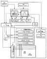
本実施例では、実施例1の第2の表示装置に接続する外部回路の構成を図12を用いて
示す。In this embodiment, the configuration of an external circuit connected to the second display device of Embodiment 1 is shown with reference to FIG.
図12の液晶表示装置は、基板上に形成されたTFTによって画素920から成る画素
部921、画素部の駆動に用いるソース側駆動回路915、ゲート信号側駆動回路914
が形成されている。ソース側駆動回路915はデジタル駆動の例を示しているが、シフト
レジスタ916、ラッチ回路917a、917b、D/Aコンバータ918、バッファ回
路919から成っている。また、ゲート信号側駆動回路914であり、シフトレジスタ、
バッファ等(いずれも図示せず)を有している。The liquid crystal display device in FIG. 12 includes a
Is formed. The source side driver circuit 915 is shown as an example of digital driving, but includes a shift register 916, latch circuits 917a and 917b, a D / A converter 918, and a buffer circuit 919. The gate signal
It has a buffer and the like (both not shown).
この液晶表示装置に接続する外部回路の構成は、安定化電源と高速高精度のオペアンプ
からなる電源回路901、USB端子などを備えた外部インターフェイスポート902、
CPU903、入力手段として用いるタッチ入力タブレット910及び検出回路911、
クロック信号発振器912、コントロール回路913などから成っている。なお、タッチ
入力タブレット910(及び検出回路911)は第2の表示装置内部に一体形成してもよ
い。The configuration of the external circuit connected to the liquid crystal display device includes a
A
CPU903は映像信号処理回路904やタッチ入力タブレット910からの信号を入
力するタブレットインターフェイス905などが内蔵されている。また、VRAM906
、DRAM907、フラッシュメモリ908及びメモリーカード909が接続されている
。CPU903で処理された情報は、映像信号として映像信号処理回路904からコント
ロール回路913に出力する。コントロール回路913は、映像信号とクロックを、ソー
ス側駆動回路915とゲート信号側駆動回路914のそれぞれのタイミング仕様に変換す
る機能を持っている。具体的には、映像信号を表示装置の各画素に対応したデータに振り
分ける機能と、外部から入力される水平同期信号及び垂直同期信号を、駆動回路のスター
ト信号及び内蔵電源回路の交流化のタイミング制御信号に変換する機能を持っている。The
A
また、コントロール回路913は、ICチップを用いてCOG法で装着してもよいし、
液晶表示装置内部に一体形成してもよい。Further, the
The liquid crystal display device may be integrally formed.
また、本実施例は、実施例1乃至6のいずれか一と自由に組み合わせることが可能であ
る。In addition, this embodiment can be freely combined with any one of Embodiments 1 to 6.
本実施例では、実施例1〜実施例8に記載の第1の表示装置または第2の表示装置とな
るEL表示装置の各画素に撮像素子(フォトダイオード)を組み込んだ例を示す。In this embodiment, an example in which an imaging element (photodiode) is incorporated in each pixel of an EL display device serving as the first display device or the second display device described in Embodiments 1 to 8 will be described.
図13に画素1002の詳しい構成を示す。点線で囲まれた領域が画素1002である
。FIG. 13 shows a detailed configuration of the pixel 1002. A region surrounded by a dotted line is a pixel 1002.
画素1002はスイッチング用TFT1004、EL駆動用TFT1005、EL素子
1006を有している。また図13では画素1002にコンデンサ1007が設けられて
いるが、コンデンサ1007を設けなくとも良い。The pixel 1002 includes a switching TFT 1004, an EL driving TFT 1005, and an EL element 1006. In FIG. 13, the capacitor 1007 is provided in the pixel 1002; however, the capacitor 1007 is not necessarily provided.
EL素子1006は陽極と陰極と、陽極と陰極との間に設けられたEL層とからなる。
陰極がEL駆動用TFT1005のソース領域またはドレイン領域と接続している場合、
陽極が対向電極、陰極が画素電極となり、発光方向が下方出射となる。逆に陽極がEL駆
動用TFT1005のソース領域またはドレイン領域と接続している場合、陽極が画素電
極、陰極が対向電極となり、発光方向が上方出射となる。The EL element 1006 includes an anode, a cathode, and an EL layer provided between the anode and the cathode.
When the cathode is connected to the source region or drain region of the EL driving TFT 1005,
The anode is a counter electrode, the cathode is a pixel electrode, and the light emission direction is downward emission. On the other hand, when the anode is connected to the source region or drain region of the EL driving TFT 1005, the anode serves as a pixel electrode and the cathode serves as a counter electrode, and the emission direction is upward emission.
スイッチング用TFT1004のゲート電極はゲート信号線Gに接続されている。そして
スイッチング用TFT1004のソース領域とドレイン領域は、一方がソース信号線Sに
、もう一方がEL駆動用TFT1005のゲート電極に接続されている。The gate electrode of the switching TFT 1004 is connected to the gate signal line G. One of the source region and the drain region of the switching TFT 1004 is connected to the source signal line S, and the other is connected to the gate electrode of the EL driving TFT 1005.
EL駆動用TFT1005のソース領域は電源供給線Vに接続されており、EL駆動用
TFT1005のドレイン領域は、EL素子1006に接続されている。コンデンサ10
07はEL駆動用TFT1005のゲート電極と電源供給線Vとに接続して設けられてい
る。The source region of the EL driving TFT 1005 is connected to the power supply line V, and the drain region of the EL driving TFT 1005 is connected to the EL element 1006. Capacitor 10
07 is connected to the gate electrode of the EL driving TFT 1005 and the power supply line V.
さらに画素1002は、リセット用TFT1010、バッファ用TFT1011、選択
用TFT1012、フォトダイオード1013を有している。Further, the pixel 1002 includes a reset TFT 1010, a buffer TFT 1011, a selection TFT 1012, and a photodiode 1013.
リセット用TFT1010のゲート電極はリセット用ゲート信号線RGに接続されている
。リセット用TFT1010のソース領域はセンサ用電源線VBに接続されている。セン
サ用電源線VBは常に一定の電位(基準電位)に保たれている。またリセット用TFT1
010のドレイン領域はフォトダイオード1013及びバッファ用TFT1011のゲー
ト電極に接続されている。The gate electrode of the reset TFT 1010 is connected to the reset gate signal line RG. The source region of the reset TFT 1010 is connected to the sensor power supply line VB. The sensor power supply line VB is always kept at a constant potential (reference potential). Reset TFT1
The drain region of 010 is connected to the photodiode 1013 and the gate electrode of the buffer TFT 1011.
図示しないが、フォトダイオード1013はN型半導体層と、P型半導体層と、N型半導
体層とP型半導体層の間に設けられた光電変換層とを有している。リセット用TFT10
10のドレイン領域は、具体的にはフォトダイオード1013のP型半導体層又はN型半
導体層に接続されている。Although not illustrated, the photodiode 1013 includes an N-type semiconductor layer, a P-type semiconductor layer, and a photoelectric conversion layer provided between the N-type semiconductor layer and the P-type semiconductor layer. Reset TFT10
Specifically, the drain region 10 is connected to a P-type semiconductor layer or an N-type semiconductor layer of the photodiode 1013.
バッファ用TFT1011のドレイン領域はセンサ用電源線VBに接続されており、常
に一定の基準電位に保たれている。そしてバッファ用TFT1011のソース領域は選択
用TFT1012のソース領域又はドレイン領域に接続されている。The drain region of the buffer TFT 1011 is connected to the sensor power supply line VB and is always kept at a constant reference potential. The source region of the buffer TFT 1011 is connected to the source region or drain region of the selection TFT 1012.
選択用TFT1012のゲート電極はセンサ用ゲート信号線SGに接続されている。そ
して選択用TFT1012のソース領域とドレイン領域は、一方は上述したとおりバッフ
ァ用TFT1011のソース領域に接続されており、もう一方はセンサ出力配線SSに接
続されている。センサ出力配線SSは定電流電源1003に接続されており、常に一定の
電流が流れている。The gate electrode of the selection TFT 1012 is connected to the sensor gate signal line SG. One of the source region and the drain region of the selection TFT 1012 is connected to the source region of the buffer TFT 1011 as described above, and the other is connected to the sensor output wiring SS. The sensor output wiring SS is connected to a constant current power source 1003, and a constant current always flows.
また、図14に本実施例の断面図を示す。1101はスイッチング用TFT、1102
はEL駆動用TFT、1103はリセット用TFT、1104はバッファ用TFT、11
05は選択用TFTである。FIG. 14 shows a cross-sectional view of this embodiment. 1101 is a switching TFT, 1102
Is an EL driving TFT, 1103 is a reset TFT, 1104 is a buffer TFT, 11
Reference numeral 05 denotes a selection TFT.
また、1108はP型半導体層、1109は光電変換層、1107はN型半導体層であ
る。P型半導体層1108と、光電変換層1109と、N型半導体層1107とによって
、フォトダイオード1106が形成される。1111はセンサ用配線であり、P型半導体
層1108と外部の電源とを電気的に接続している。
また、フォトダイオード1106のP型半導体層1108とリセット用TFT1103の
ドレイン領域とは電気的に接続されている。
Further, the P-
また1110は画素電極(陽極)、1112はEL層、1113は対向電極(陰極)で
ある。画素電極(陽極)1110と、EL層1112と、対向電極(陰極)1113とで
EL素子1114が形成される。なお1115はバンクであり、隣り合う画素同士のEL
層1112を区切っている。
1116は被写体であり、EL素子1114から発せられた光が被写体1116におい
て反射し、フォトダイオード1106に照射される。本実施例では、被写体を基板110
0のTFTが形成されていない側に設ける。
Provided on the side where no TFT is formed.
本実施例において、スイッチング用TFT1101、バッファ用TFT1104、選択
用TFT1105は全てNチャネル型TFTである。またEL駆動用TFT1102、リ
セット用TFT1103はPチャネル型TFTである。なお本発明はこの構成に限定され
ない。よってスイッチング用TFT1101、EL駆動用TFT1102、バッファ用T
FT1104、選択用TFT1105、リセット用TFT1103は、Nチャネル型TF
TとPチャネル型TFTのどちらでも良い。In this embodiment, the switching TFT 1101, the buffer TFT 1104, and the selection TFT 1105 are all N-channel TFTs. Further, the EL driving TFT 1102 and the reset TFT 1103 are P-channel TFTs. The present invention is not limited to this configuration. Therefore, switching TFT 1101, EL driving TFT 1102, buffer T
FT 1104, selection TFT 1105, reset TFT 1103 are N-channel type TF
Either T or P-channel TFT may be used.
ただし、本実施例のように、EL駆動用TFT1102のソース領域またはドレイン領
域がEL素子1114の陽極1110と電気的に接続されている場合、EL駆動用TFT
1102はPチャネル型TFTであることが望ましい。また逆に、EL駆動用TFT11
02のソース領域またはドレイン領域がEL素子1114の陰極と電気的に接続されてい
る場合、EL駆動用TFT1102はNチャネル型TFTであることが望ましい。However, when the source region or drain region of the EL driving TFT 1102 is electrically connected to the
1102 is preferably a P-channel TFT. Conversely, EL driving TFT 11
When the 02 source region or drain region is electrically connected to the cathode of the EL element 1114, the EL driving TFT 1102 is preferably an N-channel TFT.
なお、本実施例のフォトダイオードは他のTFTと同時に形成することができるので、
工程数を抑えることができる。Since the photodiode of this embodiment can be formed at the same time as other TFTs,
The number of processes can be reduced.
なお、本実施例は、実施例1〜実施例7と自由に組み合わせることが可能である。 In addition, a present Example can be freely combined with Example 1-7.
本実施例では、実施例1〜実施例8に記載の第1の表示装置または第2の表示装置とな
るEL表示装置の各画素にメモリー素子(SRAM)を組み込んだ例を示す。図15に画
素1504の拡大図を示す。In this embodiment, an example in which a memory element (SRAM) is incorporated in each pixel of an EL display device serving as the first display device or the second display device described in Embodiments 1 to 8 will be described. FIG. 15 shows an enlarged view of the pixel 1504.
図15において、1505はスイッチング用TFTである。スイッチング用TFT140
5のゲート電極は、ゲート信号を入力するゲート信号線(G1〜Gn)
のうちの1つであるゲート信号線1506に接続されている。スイッチングTFT150
5のソース領域とドレイン領域は、一方が信号を入力するソース信号線(S1〜Sn)の
うちの1つであるソース信号線1507に、もう一方がSRAM1508の入力側に接続
されている。SRAM1508の出力側は電流制御用TFT1509のゲート電極に接続
されている。In FIG. 15, reference numeral 1505 denotes a switching TFT. Switching TFT140
5 is a gate signal line (G1 to Gn) for inputting a gate signal.
Are connected to a gate signal line 1506, which is one of them. Switching TFT150
One of the source region and the drain region is connected to a
また、電流制御用TFT1509のソース領域とドレイン領域は、一方が電流供給線(
V1〜Vn)の1つである電流供給線1510に接続され、もう一方はEL素子1511
に接続される。One of the source region and the drain region of the
V1 to Vn) is connected to a
Connected to.
EL素子1511は陽極と陰極と、陽極と陰極との間に設けられたEL層とからなる。
陽極が電流制御用TFT1509のソース領域またはドレイン領域と接続している場合、
言い換えると陽極が画素電極の場合、陰極は対向電極となる。
逆に陰極が電流制御用TFT1509のソース領域またはドレイン領域と接続している場
合、言い換えると陰極が画素電極の場合、陽極は対向電極となる。The
When the anode is connected to the source region or drain region of the
In other words, when the anode is a pixel electrode, the cathode is a counter electrode.
Conversely, when the cathode is connected to the source region or drain region of the
SRAM1508はpチャネル型TFTとnチャネル型TFTを2つずつ有しており、
pチャネル型TFTのソース領域は高電圧側のVddhに、nチャネル型TFTのソース
領域は低電圧側のVssに、それぞれ接続されている。1つのpチャネル型TFTと1つ
のnチャネル型TFTとが対になっており、1つのSRAMの中にpチャネル型TFTと
nチャネル型TFTとの対が2組存在することになる。The
The source region of the p-channel TFT is connected to Vddh on the high voltage side, and the source region of the n-channel TFT is connected to Vss on the low voltage side. One p-channel TFT and one n-channel TFT are paired, and two pairs of p-channel TFT and n-channel TFT exist in one SRAM.
また、対になったpチャネル型TFTとnチャネル型TFTは、そのドレイン領域が互
いに接続されている。また対になったpチャネル型TFTとnチャネル型TFTは、その
ゲート電極が互いに接続されている。そして互いに、一方の対になっているpチャネル型
TFT及びnチャネル型TFTのドレイン領域が、他の一方の対になっているpチャネル
型TFT及びnチャネル型TFTのゲート電極と同じ電位に保たれている。The drain regions of the paired p-channel TFT and n-channel TFT are connected to each other. The gate electrodes of the paired p-channel TFT and n-channel TFT are connected to each other. The drain regions of one pair of p-channel TFT and n-channel TFT are kept at the same potential as the gate electrode of the other pair of p-channel TFT and n-channel TFT. I'm leaning.
そして一方の対になっているpチャネル型及びnチャネル型TFTのドレイン領域は入
力の信号(Vin)が入る入力側であり、もう一方の対になっているpチャネル型及びn
チャネル型TFTのドレイン領域は出力の信号(Vout)が出力される出力側である。The drain region of one pair of p-channel and n-channel TFTs is an input side for receiving an input signal (Vin), and the other pair of p-channel and n-channel TFTs.
The drain region of the channel type TFT is an output side from which an output signal (Vout) is output.
SRAMはVinを保持し、Vinを反転させた信号であるVoutを出力するように
設計されている。つまり、VinがHiだとVoutはVss相当のLoの信号となり、
VinがLoだとVoutはVddh相当のHiの信号となる。The SRAM is designed to hold Vin and output Vout that is a signal obtained by inverting Vin. That is, when Vin is Hi, Vout becomes a Lo signal corresponding to Vss.
When Vin is Lo, Vout is a Hi signal corresponding to Vddh.
なお、本実施例で示すように、SRAMが画素1504に一つ設けられている場合には
、画素中のメモリーデータが保持されているため外部回路の大半を止めた状態で静止画を
表示することが可能である。これにより、低消費電力化を実現することができる。As shown in this embodiment, when one SRAM is provided in the pixel 1504, since the memory data in the pixel is held, a still image is displayed with most of the external circuits stopped. It is possible. Thereby, low power consumption can be realized.
また、画素に複数のSRAMを設けることも可能であり、SRAMを複数設けた場合に
は、複数のデータを保持することができるので、時間階調による階調表示を可能になる。In addition, a plurality of SRAMs can be provided in a pixel. When a plurality of SRAMs are provided, a plurality of data can be held, so that gradation display by time gradation can be performed.
なお、本実施例の構成は、実施例1〜実施例9のいずれの構成とも自由に組み合わせて
実施することが可能である。In addition, the structure of a present Example can be implemented in combination with any structure of Example 1- Example 9 freely.
Claims (1)
Translated fromJapanese前記第1の基板に対向する第2の基板と、
前記第1の基板上の画素部と、
タッチ入力操作部と、
タッチ入力操作部に接続された検出回路と、
前記第1の基板と前記第2の基板の間の第1のシール材と、
前記第1の基板と前記第2の基板の間の第2のシール材と、
を有する携帯型電子機器であって、
前記第2のシール材は、前記第1のシール材と接触する第1の領域を有し、
前記第2のシール材は、前記第2の基板の端部と接触する第2の領域を有し、
前記画素部は画素を有し、
前記画素は少なくとも5つの薄膜トランジスタと、EL素子と、を有し、
前記EL素子は、第1の電極と、第2の電極と、を有し、
前記第1の電極は、前記5つの薄膜トランジスタの一つと電気的に接続し、
前記EL素子は、第1の膜で覆われ、
前記第1の電極の端部は、第2の膜で覆われていることを特徴とする携帯型電子機器。A first substrate;
A second substrate facing the first substrate;
A pixel portion on the first substrate;
A touch input operation unit;
A detection circuit connected to the touch input operation unit;
A first sealant between the first substrate and the second substrate;
A second sealant between the first substrate and the second substrate;
A portable electronic device having
The second sealing material has a first region in contact with the first sealing material,
The second sealing material has a second region in contact with an end of the second substrate,
The pixel portion has a pixel,
The pixel has at least five thin film transistors and an EL element,
The EL element has a first electrode and a second electrode,
The first electrode is electrically connected to one of the five thin film transistors;
The EL element is covered with a first film,
A portable electronic device, wherein an end portion of the first electrode is covered with a second film.
Priority Applications (1)
| Application Number | Priority Date | Filing Date | Title |
|---|---|---|---|
| JP2012173592AJP2012213237A (en) | 2000-08-23 | 2012-08-06 | Portable electronic appliance |
Applications Claiming Priority (3)
| Application Number | Priority Date | Filing Date | Title |
|---|---|---|---|
| JP2000252717 | 2000-08-23 | ||
| JP2000252717 | 2000-08-23 | ||
| JP2012173592AJP2012213237A (en) | 2000-08-23 | 2012-08-06 | Portable electronic appliance |
Related Parent Applications (1)
| Application Number | Title | Priority Date | Filing Date |
|---|---|---|---|
| JP2011014923ADivisionJP2011135592A (en) | 2000-08-23 | 2011-01-27 | Electronic device |
Publications (1)
| Publication Number | Publication Date |
|---|---|
| JP2012213237Atrue JP2012213237A (en) | 2012-11-01 |
Family
ID=18741917
Family Applications (9)
| Application Number | Title | Priority Date | Filing Date |
|---|---|---|---|
| JP2011014923AWithdrawnJP2011135592A (en) | 2000-08-23 | 2011-01-27 | Electronic device |
| JP2012173592AWithdrawnJP2012213237A (en) | 2000-08-23 | 2012-08-06 | Portable electronic appliance |
| JP2012173596AWithdrawnJP2013033255A (en) | 2000-08-23 | 2012-08-06 | Portable electronic apparatus |
| JP2012241722AWithdrawnJP2013021737A (en) | 2000-08-23 | 2012-11-01 | Portable electronic apparatus |
| JP2013120602AWithdrawnJP2013225883A (en) | 2000-08-23 | 2013-06-07 | Electronic apparatus |
| JP2014085406AWithdrawnJP2014140250A (en) | 2000-08-23 | 2014-04-17 | Mobile phone |
| JP2015144794AWithdrawnJP2016001887A (en) | 2000-08-23 | 2015-07-22 | Electronic apparatus |
| JP2018080822AWithdrawnJP2018156088A (en) | 2000-08-23 | 2018-04-19 | Electronics |
| JP2019185906AWithdrawnJP2020107319A (en) | 2000-08-23 | 2019-10-09 | Electronic apparatus |
Family Applications Before (1)
| Application Number | Title | Priority Date | Filing Date |
|---|---|---|---|
| JP2011014923AWithdrawnJP2011135592A (en) | 2000-08-23 | 2011-01-27 | Electronic device |
Family Applications After (7)
| Application Number | Title | Priority Date | Filing Date |
|---|---|---|---|
| JP2012173596AWithdrawnJP2013033255A (en) | 2000-08-23 | 2012-08-06 | Portable electronic apparatus |
| JP2012241722AWithdrawnJP2013021737A (en) | 2000-08-23 | 2012-11-01 | Portable electronic apparatus |
| JP2013120602AWithdrawnJP2013225883A (en) | 2000-08-23 | 2013-06-07 | Electronic apparatus |
| JP2014085406AWithdrawnJP2014140250A (en) | 2000-08-23 | 2014-04-17 | Mobile phone |
| JP2015144794AWithdrawnJP2016001887A (en) | 2000-08-23 | 2015-07-22 | Electronic apparatus |
| JP2018080822AWithdrawnJP2018156088A (en) | 2000-08-23 | 2018-04-19 | Electronics |
| JP2019185906AWithdrawnJP2020107319A (en) | 2000-08-23 | 2019-10-09 | Electronic apparatus |
Country Status (2)
| Country | Link |
|---|---|
| US (8) | US7430025B2 (en) |
| JP (9) | JP2011135592A (en) |
Families Citing this family (71)
| Publication number | Priority date | Publication date | Assignee | Title |
|---|---|---|---|---|
| US7430025B2 (en) | 2000-08-23 | 2008-09-30 | Semiconductor Energy Laboratory Co., Ltd. | Portable electronic device |
| JP4831892B2 (en) | 2001-07-30 | 2011-12-07 | 株式会社半導体エネルギー研究所 | Semiconductor device |
| TWI273539B (en)* | 2001-11-29 | 2007-02-11 | Semiconductor Energy Lab | Display device and display system using the same |
| US7053967B2 (en) | 2002-05-23 | 2006-05-30 | Planar Systems, Inc. | Light sensitive display |
| US7009663B2 (en)* | 2003-12-17 | 2006-03-07 | Planar Systems, Inc. | Integrated optical light sensitive active matrix liquid crystal display |
| AU2002336341A1 (en) | 2002-02-20 | 2003-09-09 | Planar Systems, Inc. | Light sensitive display |
| US6775560B2 (en) | 2002-05-31 | 2004-08-10 | Lavaflow, Llp | Cellular telephone having a touch screen user interface |
| US20040058714A1 (en)* | 2002-06-28 | 2004-03-25 | Rohm Co., Ltd. | Portable communicating apparatus |
| AU2003289348A1 (en)* | 2002-12-27 | 2004-07-29 | Semiconductor Energy Laboratory Co., Ltd. | Display and electronic device |
| JP4251874B2 (en)* | 2003-01-21 | 2009-04-08 | 三洋電機株式会社 | Electroluminescence display device |
| CN101819984B (en) | 2003-01-24 | 2014-04-30 | 株式会社半导体能源研究所 | Electronic book |
| US20080084374A1 (en)* | 2003-02-20 | 2008-04-10 | Planar Systems, Inc. | Light sensitive display |
| US7333072B2 (en)* | 2003-03-24 | 2008-02-19 | Semiconductor Energy Laboratory Co., Ltd. | Thin film integrated circuit device |
| JP4614633B2 (en) | 2003-04-09 | 2011-01-19 | 株式会社半導体エネルギー研究所 | Electronics |
| US20120081315A1 (en) | 2010-10-01 | 2012-04-05 | Imerj LLC | Keyboard spanning multiple screens |
| JP4702516B2 (en) | 2003-05-07 | 2011-06-15 | エルジー エレクトロニクス インコーポレイティド | Organic EL device and manufacturing method thereof |
| GB2413915B (en)* | 2004-05-04 | 2007-12-05 | Yogesh Kumar Kanhye | Mobile phone |
| KR100751318B1 (en)* | 2004-10-26 | 2007-08-22 | 삼성에스디아이 주식회사 | Joining method of sheet material, sheet joining structure and display module having same |
| JP4692986B2 (en)* | 2004-12-17 | 2011-06-01 | 株式会社 日立ディスプレイズ | Display device |
| US7706677B2 (en)* | 2005-01-14 | 2010-04-27 | Samsung Electro-Mechanics Co., Ltd | Mobile communication terminal device |
| KR100552451B1 (en)* | 2005-07-27 | 2006-02-21 | 실리콘 디스플레이 (주) | Unevenness detecting device which compensates threshold voltage and method thereof |
| KR20070034767A (en)* | 2005-09-26 | 2007-03-29 | 엘지전자 주식회사 | Mobile communication terminal having multiple display areas and data display method between displays using same |
| JP4791165B2 (en)* | 2005-12-07 | 2011-10-12 | 富士フイルム株式会社 | camera |
| JP5048271B2 (en)* | 2006-05-02 | 2012-10-17 | 任天堂株式会社 | GAME PROGRAM AND GAME DEVICE |
| JP4285524B2 (en)* | 2006-10-13 | 2009-06-24 | セイコーエプソン株式会社 | Electro-optical device and electronic apparatus |
| KR100827115B1 (en) | 2006-12-04 | 2008-05-02 | 삼성전자주식회사 | Method for implementing preview function and terminal for same |
| JP5134327B2 (en)* | 2007-09-26 | 2013-01-30 | 株式会社ジャパンディスプレイイースト | Display device |
| JP5095814B2 (en)* | 2008-08-25 | 2012-12-12 | 日本写真印刷株式会社 | Touch input device and electronic device |
| US20100218249A1 (en)* | 2009-02-25 | 2010-08-26 | Microsoft Corporation | Authentication via a device |
| JP5553707B2 (en) | 2009-08-21 | 2014-07-16 | 株式会社半導体エネルギー研究所 | Photodetector |
| TWI498786B (en)* | 2009-08-24 | 2015-09-01 | Semiconductor Energy Lab | Touch sensor and method for driving the same and display device |
| TWI523240B (en)* | 2009-08-24 | 2016-02-21 | 半導體能源研究所股份有限公司 | Photodetector and display device |
| KR101056284B1 (en)* | 2009-10-22 | 2011-08-11 | 삼성모바일디스플레이주식회사 | Sensor Scan Driver and Flat Panel Display with Touch Screen |
| US8442600B1 (en)* | 2009-12-02 | 2013-05-14 | Google Inc. | Mobile electronic device wrapped in electronic display |
| EP2365417A3 (en)* | 2010-03-08 | 2015-04-29 | Semiconductor Energy Laboratory Co, Ltd. | Electronic device and electronic system |
| WO2011135988A1 (en) | 2010-04-28 | 2011-11-03 | Semiconductor Energy Laboratory Co., Ltd. | Semiconductor display device and driving method the same |
| US9046992B2 (en) | 2010-10-01 | 2015-06-02 | Z124 | Gesture controls for multi-screen user interface |
| KR101843559B1 (en) | 2010-11-05 | 2018-03-30 | 가부시키가이샤 한도오따이 에네루기 켄큐쇼 | Display device with imaging function and method for driving the same |
| US9310923B2 (en) | 2010-12-03 | 2016-04-12 | Apple Inc. | Input device for touch sensitive devices |
| KR101860859B1 (en)* | 2011-06-13 | 2018-05-25 | 삼성디스플레이 주식회사 | Manufacturing method of thin film transistor, the thin film transistor manufactured by the same, manufacturing method of organic light emitting apparatus and the organic light emitting apparatus manufactured by the same |
| US8638320B2 (en) | 2011-06-22 | 2014-01-28 | Apple Inc. | Stylus orientation detection |
| US9329703B2 (en) | 2011-06-22 | 2016-05-03 | Apple Inc. | Intelligent stylus |
| US8928635B2 (en) | 2011-06-22 | 2015-01-06 | Apple Inc. | Active stylus |
| KR101819980B1 (en)* | 2011-09-09 | 2018-01-19 | 삼성전자주식회사 | Light sensing apparatus and method of driving the light sensing apparatus, and optical touch screen apparatus including the light sensing apparatus |
| US9182935B2 (en) | 2011-09-27 | 2015-11-10 | Z124 | Secondary single screen mode activation through menu option |
| JP2013101420A (en)* | 2011-11-07 | 2013-05-23 | Japan Display West Co Ltd | Display device and electronic apparatus |
| CN103246320B (en)* | 2012-02-10 | 2016-12-14 | 联想(北京)有限公司 | Terminal unit |
| US9147706B2 (en) | 2012-05-29 | 2015-09-29 | Semiconductor Energy Laboratory Co., Ltd. | Semiconductor device having sensor circuit having amplifier circuit |
| US20140029190A1 (en)* | 2012-07-25 | 2014-01-30 | Kabushiki Kaisha Toshiba | Electronic device |
| US9557845B2 (en) | 2012-07-27 | 2017-01-31 | Apple Inc. | Input device for and method of communication with capacitive devices through frequency variation |
| US9652090B2 (en) | 2012-07-27 | 2017-05-16 | Apple Inc. | Device for digital communication through capacitive coupling |
| US9176604B2 (en) | 2012-07-27 | 2015-11-03 | Apple Inc. | Stylus device |
| US10048775B2 (en) | 2013-03-14 | 2018-08-14 | Apple Inc. | Stylus detection and demodulation |
| KR20160010487A (en) | 2013-05-21 | 2016-01-27 | 가부시키가이샤 한도오따이 에네루기 켄큐쇼 | Light-emitting device and camera |
| JP2015028918A (en) | 2013-06-27 | 2015-02-12 | 株式会社半導体エネルギー研究所 | Light-emitting device and camera |
| KR102398137B1 (en)* | 2013-07-02 | 2022-05-17 | 가부시키가이샤 한도오따이 에네루기 켄큐쇼 | Data processing device |
| US10067580B2 (en) | 2013-07-31 | 2018-09-04 | Apple Inc. | Active stylus for use with touch controller architecture |
| US9758256B1 (en)* | 2013-08-06 | 2017-09-12 | The Boeing Company | Pilot-configurable information on a display unit |
| KR102136836B1 (en) | 2013-09-09 | 2020-08-13 | 삼성전자주식회사 | Wearable device performing user authentication by using bio-signals and authentication method of the wearable device |
| DE102013112489B4 (en)* | 2013-11-13 | 2022-07-28 | Pictiva Displays International Limited | Flat light-emitting component for a flashlight device, flashlight device and electronic device comprising a flashlight device |
| US9310946B2 (en)* | 2014-01-23 | 2016-04-12 | Top Victory Investments Limited | Capacitive-type touch control display |
| US10067618B2 (en) | 2014-12-04 | 2018-09-04 | Apple Inc. | Coarse scan and targeted active mode scan for touch |
| CN104706334B (en)* | 2015-03-30 | 2017-08-11 | 京东方科技集团股份有限公司 | A kind of display panel and display device with health monitoring function |
| CN105137633B (en) | 2015-07-29 | 2018-04-20 | 武汉华星光电技术有限公司 | Display panel and thin-film transistor array base-plate |
| US10474277B2 (en) | 2016-05-31 | 2019-11-12 | Apple Inc. | Position-based stylus communication |
| CN106326845B (en)* | 2016-08-15 | 2017-08-11 | 京东方科技集团股份有限公司 | Fingerprint identification unit and preparation method, array base palte, display device and fingerprint identification method |
| CN208077524U (en)* | 2018-03-23 | 2018-11-09 | 京东方科技集团股份有限公司 | A kind of display device |
| WO2020034077A1 (en)* | 2018-08-14 | 2020-02-20 | Huawei Technologies Co., Ltd. | Display device and display data generating method |
| CN111694264B (en)* | 2019-03-12 | 2021-08-27 | 深圳市知赢科技有限公司 | Smart watch, control method thereof and readable storage medium |
| CN111031253B (en)* | 2020-01-13 | 2021-07-06 | 维沃移动通信有限公司 | A shooting method and electronic device |
| US12153764B1 (en) | 2020-09-25 | 2024-11-26 | Apple Inc. | Stylus with receive architecture for position determination |
Citations (6)
| Publication number | Priority date | Publication date | Assignee | Title |
|---|---|---|---|---|
| WO1997014244A1 (en)* | 1995-10-11 | 1997-04-17 | Sony Corporation | Information providing device and portable communication terminal |
| JPH1091342A (en)* | 1996-09-12 | 1998-04-10 | Sanyo Electric Co Ltd | Portable information terminal |
| JPH10319872A (en)* | 1997-01-17 | 1998-12-04 | Xerox Corp | Active matrix organic light emitting diode display |
| JPH11122398A (en)* | 1997-10-09 | 1999-04-30 | Sony Corp | Portable communication terminal, image display control method, device and method for transmitting image information and transmission medium |
| JPH11327715A (en)* | 1998-05-14 | 1999-11-30 | Sony Corp | Information processor |
| JP2000223715A (en)* | 1998-11-25 | 2000-08-11 | Semiconductor Energy Lab Co Ltd | Method for manufacturing thin film transistor and method for manufacturing active matrix substrate |
Family Cites Families (118)
| Publication number | Priority date | Publication date | Assignee | Title |
|---|---|---|---|---|
| JPS5810481U (en)* | 1981-07-10 | 1983-01-22 | シャープ株式会社 | liquid crystal display device |
| US4809078A (en)* | 1983-10-05 | 1989-02-28 | Casio Computer Co., Ltd. | Liquid crystal television receiver |
| GB2150726B (en)* | 1983-11-30 | 1988-01-20 | Standard Telephones Cables Ltd | Office terminals |
| US4719152A (en)* | 1984-09-21 | 1988-01-12 | Konishiroku Photo Industry Co., Ltd. | Transparent conductive layer built-up material |
| JPS62186320A (en) | 1986-02-12 | 1987-08-14 | Semiconductor Energy Lab Co Ltd | Semiconductor device |
| JPS62186320U (en) | 1986-05-16 | 1987-11-27 | ||
| JPS63118186A (en) | 1986-11-05 | 1988-05-23 | 株式会社 半導体エネルギ−研究所 | Display device |
| JPH0346467Y2 (en) | 1987-01-27 | 1991-10-01 | ||
| JPS63120286U (en)* | 1987-01-28 | 1988-08-03 | ||
| JPH0229817A (en)* | 1988-07-20 | 1990-01-31 | Fujitsu Ltd | Guidance output control system |
| US4996523A (en)* | 1988-10-20 | 1991-02-26 | Eastman Kodak Company | Electroluminescent storage display with improved intensity driver circuits |
| GB8909011D0 (en)* | 1989-04-20 | 1989-06-07 | Friend Richard H | Electroluminescent devices |
| JPH02148687U (en) | 1989-05-17 | 1990-12-18 | ||
| JP2838318B2 (en)* | 1990-11-30 | 1998-12-16 | 株式会社半導体エネルギー研究所 | Photosensitive device and manufacturing method thereof |
| JPH04239960A (en)* | 1991-01-24 | 1992-08-27 | Nec Corp | Man-machine interface system |
| GB9108226D0 (en)* | 1991-04-17 | 1991-06-05 | Philips Electronic Associated | Optical touch input device |
| JPH05298257A (en) | 1992-04-16 | 1993-11-12 | Toshiba Corp | Portable electronic devices |
| JP2800628B2 (en)* | 1993-05-11 | 1998-09-21 | セイコーエプソン株式会社 | Lighting equipment |
| KR100324989B1 (en)* | 1993-11-08 | 2002-06-24 | 마츠시타 덴끼 산교 가부시키가이샤 | Input display integrated information processing device |
| US5844538A (en)* | 1993-12-28 | 1998-12-01 | Sharp Kabushiki Kaisha | Active matrix-type image display apparatus controlling writing of display data with respect to picture elements |
| CN1230919C (en) | 1994-06-02 | 2005-12-07 | 株式会社半导体能源研究所 | Active Matrix Displays and Electro-Optic Components |
| JPH08234162A (en)* | 1995-02-27 | 1996-09-13 | Sharp Corp | Liquid crystal display device with integrated touch panel |
| JPH08241240A (en)* | 1995-03-03 | 1996-09-17 | Toshiba Corp | Computer system |
| JP3561549B2 (en)* | 1995-04-07 | 2004-09-02 | 三洋電機株式会社 | Organic electroluminescence device |
| JPH0926769A (en)* | 1995-07-10 | 1997-01-28 | Hitachi Ltd | Image display device |
| JP3838665B2 (en) | 1995-08-11 | 2006-10-25 | 株式会社 東芝 | MOS type solid-state imaging device |
| JP3966557B2 (en) | 1995-08-11 | 2007-08-29 | 株式会社東芝 | Image system, solid-state imaging device semiconductor integrated circuit used therein, and differential output method |
| WO1997007628A1 (en) | 1995-08-11 | 1997-02-27 | Kabushiki Kaisha Toshiba | Mos solid-state image pickup device |
| JP3845449B2 (en) | 1995-08-11 | 2006-11-15 | 株式会社東芝 | MOS type solid-state imaging device |
| JP3647523B2 (en)* | 1995-10-14 | 2005-05-11 | 株式会社半導体エネルギー研究所 | Matrix type liquid crystal display device |
| JPH09190284A (en)* | 1996-01-11 | 1997-07-22 | Canon Inc | Information processing apparatus and method |
| JPH09212565A (en)* | 1996-02-07 | 1997-08-15 | Nec Corp | Radio portable terminal system |
| JP3476320B2 (en)* | 1996-02-23 | 2003-12-10 | 株式会社半導体エネルギー研究所 | Semiconductor thin film and method for manufacturing the same, semiconductor device and method for manufacturing the same |
| KR100270147B1 (en)* | 1996-03-01 | 2000-10-16 | 니시무로 타이죠 | Lcd apparatus |
| JP3474700B2 (en)* | 1996-03-13 | 2003-12-08 | 株式会社東芝 | Solid-state imaging device |
| US6510325B1 (en)* | 1996-04-19 | 2003-01-21 | Mack, Ii Gawins A. | Convertible portable telephone |
| JPH09305259A (en)* | 1996-05-13 | 1997-11-28 | Hitachi Ltd | Information processing apparatus and operating method thereof |
| JP3726358B2 (en) | 1996-07-01 | 2005-12-14 | ブラザー工業株式会社 | Paper transport device |
| KR100241287B1 (en)* | 1996-09-10 | 2000-02-01 | 구본준 | A method for fabricating liquid crystal display device |
| JPH10134959A (en) | 1996-10-29 | 1998-05-22 | Sharp Corp | Thin film EL panel |
| JPH10145476A (en)* | 1996-11-08 | 1998-05-29 | Casio Comput Co Ltd | Electronic device with display and operation unit |
| TW464785B (en)* | 1996-11-21 | 2001-11-21 | Seiko Epson Corp | Input device, liquid crystal device, and electronic equipment using the liquid crystal device |
| JP3899566B2 (en)* | 1996-11-25 | 2007-03-28 | セイコーエプソン株式会社 | Manufacturing method of organic EL display device |
| JPH10171757A (en)* | 1996-12-13 | 1998-06-26 | Matsushita Electric Ind Co Ltd | Information terminal |
| JPH10177430A (en)* | 1996-12-18 | 1998-06-30 | Fujitsu Ltd | Portable information processing device |
| JPH10214974A (en)* | 1997-01-28 | 1998-08-11 | Semiconductor Energy Lab Co Ltd | Semiconductor device and manufacturing method thereof |
| US6462722B1 (en)* | 1997-02-17 | 2002-10-08 | Seiko Epson Corporation | Current-driven light-emitting display apparatus and method of producing the same |
| JP3711693B2 (en) | 1997-04-03 | 2005-11-02 | セイコーエプソン株式会社 | COMMUNICATION TERMINAL DEVICE, COMMUNICATION CONTROL METHOD, AND RECORDING MEDIUM |
| JPH10288965A (en)* | 1997-04-14 | 1998-10-27 | Casio Comput Co Ltd | Display device |
| JP3592037B2 (en)* | 1997-05-30 | 2004-11-24 | キヤノン株式会社 | Photoelectric conversion device |
| US6175345B1 (en)* | 1997-06-02 | 2001-01-16 | Canon Kabushiki Kaisha | Electroluminescence device, electroluminescence apparatus, and production methods thereof |
| JP2002502568A (en)* | 1997-06-02 | 2002-01-22 | モトローラ・インコーポレイテッド | Method for authorizing a connection between devices in a capability addressable network |
| US6125286A (en)* | 1997-06-05 | 2000-09-26 | Motorola, Inc. | Communication device having multiple displays and method of operating the same |
| JP3048964B2 (en) | 1997-06-24 | 2000-06-05 | 邦彦 小池 | Telephone transmitting / receiving unit and mobile communication terminal |
| JPH1126166A (en) | 1997-06-30 | 1999-01-29 | Nec Kansai Ltd | Electroluminescent lamp and el display device with switch |
| JP3520396B2 (en) | 1997-07-02 | 2004-04-19 | セイコーエプソン株式会社 | Active matrix substrate and display device |
| JP3516328B2 (en) | 1997-08-22 | 2004-04-05 | 株式会社日立製作所 | Information communication terminal equipment |
| JPH1165763A (en) | 1997-08-22 | 1999-03-09 | Sharp Corp | Display panel and display device |
| JP3830238B2 (en) | 1997-08-29 | 2006-10-04 | セイコーエプソン株式会社 | Active matrix type device |
| JPH11167373A (en)* | 1997-10-01 | 1999-06-22 | Semiconductor Energy Lab Co Ltd | Semiconductor display device and driving method thereof |
| KR200225264Y1 (en)* | 1997-10-01 | 2001-06-01 | 김순택 | Portable display |
| US7002621B2 (en)* | 1997-10-06 | 2006-02-21 | Adair Edwin L | Communication devices incorporating reduced area imaging devices |
| JP3429440B2 (en)* | 1997-10-24 | 2003-07-22 | シャープ株式会社 | Semiconductor device and manufacturing method thereof |
| US6909419B2 (en)* | 1997-10-31 | 2005-06-21 | Kopin Corporation | Portable microdisplay system |
| DE19782261C2 (en)* | 1997-12-24 | 2002-12-12 | Mitsubishi Electric Corp | Attachment construction for a flexible liquid crystal display panel |
| JPH11224781A (en)* | 1998-02-05 | 1999-08-17 | Pioneer Electron Corp | Organic EL display and manufacturing method thereof |
| DE69925216T2 (en) | 1998-03-12 | 2005-10-06 | Seiko Epson Corp. | ACTIVE MATRIX LIGHT EMITTING DEVICE AND MANUFACTURING METHOD |
| JP3629939B2 (en) | 1998-03-18 | 2005-03-16 | セイコーエプソン株式会社 | Transistor circuit, display panel and electronic device |
| JP3997368B2 (en)* | 1998-04-30 | 2007-10-24 | ソニー株式会社 | Information communication terminal |
| GB2372665B (en)* | 1998-05-08 | 2002-11-27 | Orange Personal Comm Serv Ltd | Mobile communications |
| JP3508546B2 (en)* | 1998-05-11 | 2004-03-22 | 日本電気株式会社 | Screen operation system and screen operation method |
| JPH11329739A (en)* | 1998-05-11 | 1999-11-30 | Oki Electric Ind Co Ltd | Organic EL device and method of manufacturing the same |
| JPH11326874A (en) | 1998-05-15 | 1999-11-26 | Seiko Epson Corp | Reflective liquid crystal device and reflective projector |
| JP2000003652A (en) | 1998-06-16 | 2000-01-07 | Fujikura Ltd | In-vehicle input device |
| US6158884A (en)* | 1998-06-26 | 2000-12-12 | Motorola, Inc. | Integrated communicative watch |
| JP4185588B2 (en)* | 1998-07-23 | 2008-11-26 | キヤノン株式会社 | Image display device |
| JP3624703B2 (en) | 1998-07-28 | 2005-03-02 | セイコーエプソン株式会社 | Electro-optical device and projection display device using the same |
| JP2000227784A (en) | 1998-07-29 | 2000-08-15 | Seiko Epson Corp | Driving circuit of electro-optical device and electro-optical device |
| JP4386978B2 (en)* | 1998-08-07 | 2009-12-16 | 株式会社半導体エネルギー研究所 | Method for manufacturing semiconductor device |
| US6181300B1 (en)* | 1998-09-09 | 2001-01-30 | Ati Technologies | Display format conversion circuit with resynchronization of multiple display screens |
| JP2000099304A (en) | 1998-09-24 | 2000-04-07 | Canon Inc | Image forming device |
| JP4338845B2 (en) | 1998-10-02 | 2009-10-07 | 株式会社半導体エネルギー研究所 | Touch panel, display device including touch panel, and electronic apparatus including display device |
| US6972753B1 (en) | 1998-10-02 | 2005-12-06 | Semiconductor Energy Laboratory Co., Ltd. | Touch panel, display device provided with touch panel and electronic equipment provided with display device |
| JP2000122615A (en)* | 1998-10-09 | 2000-04-28 | Casio Comput Co Ltd | Image display control device, image display control method, and recording medium storing image display control program |
| JP3475809B2 (en) | 1998-10-14 | 2003-12-10 | 株式会社デンソー | Portable videophone |
| US6274887B1 (en) | 1998-11-02 | 2001-08-14 | Semiconductor Energy Laboratory Co., Ltd. | Semiconductor device and manufacturing method therefor |
| WO2000028370A1 (en)* | 1998-11-06 | 2000-05-18 | Kopin Corporation | Microdisplay viewer |
| JP3011209B1 (en) | 1998-11-16 | 2000-02-21 | 日本電気株式会社 | Image sensor |
| KR100317281B1 (en)* | 1998-11-20 | 2002-01-15 | 구자홍 | method for driving self-emmitting display device |
| US6277679B1 (en) | 1998-11-25 | 2001-08-21 | Semiconductor Energy Laboratory Co., Ltd. | Method of manufacturing thin film transistor |
| JP3901893B2 (en)* | 1998-11-25 | 2007-04-04 | 株式会社半導体エネルギー研究所 | Semiconductor device and manufacturing method thereof |
| JP2000172199A (en) | 1998-12-01 | 2000-06-23 | Sanyo Electric Co Ltd | Electroluminescence display device |
| JP2000184026A (en) | 1998-12-14 | 2000-06-30 | Samsung Sdi Co Ltd | Portable communication device |
| JP2000181423A (en)* | 1998-12-18 | 2000-06-30 | Kyocera Corp | Multi-monitor |
| JP2000201213A (en)* | 1999-01-06 | 2000-07-18 | Nippon Telegr & Teleph Corp <Ntt> | Recording method for portable memory during call and call terminal with editing function |
| JP2000208519A (en) | 1999-01-18 | 2000-07-28 | Seiko Epson Corp | Low resistance film, active matrix substrate, electro-optical device and electronic equipment |
| JP4379939B2 (en)* | 1999-01-27 | 2009-12-09 | ソニー株式会社 | Fingerprint image acquisition device and fingerprint verification device |
| US6346730B1 (en)* | 1999-04-06 | 2002-02-12 | Semiconductor Energy Laboratory Co., Ltd. | Liquid crystal display device having a pixel TFT formed in a display region and a drive circuit formed in the periphery of the display region on the same substrate |
| JP5210473B2 (en)* | 1999-06-21 | 2013-06-12 | 株式会社半導体エネルギー研究所 | Display device |
| JP2001035652A (en) | 1999-07-21 | 2001-02-09 | Matsushita Electric Ind Co Ltd | ELECTROLUMINESCENT ELEMENT AND LIGHTING UNIT USING SAME |
| GB9919536D0 (en)* | 1999-08-19 | 1999-10-20 | Koninkl Philips Electronics Nv | Active matrix electroluminescent display device |
| US6384427B1 (en) | 1999-10-29 | 2002-05-07 | Semiconductor Energy Laboratory Co., Ltd. | Electronic device |
| US6646287B1 (en) | 1999-11-19 | 2003-11-11 | Semiconductor Energy Laboratory Co., Ltd. | Semiconductor device with tapered gate and insulating film |
| TW480727B (en)* | 2000-01-11 | 2002-03-21 | Semiconductor Energy Laboratro | Semiconductor display device |
| US7113231B2 (en)* | 2000-02-14 | 2006-09-26 | 3M Innovative Properties Company | Dot-sequential color display system |
| JP3796412B2 (en)* | 2000-02-28 | 2006-07-12 | キヤノン株式会社 | Imaging device |
| US7194085B2 (en) | 2000-03-22 | 2007-03-20 | Semiconductor Energy Laboratory Co., Ltd. | Electronic device |
| JP2001339492A (en) | 2000-03-22 | 2001-12-07 | Semiconductor Energy Lab Co Ltd | Electronic equipment |
| US20020049714A1 (en) | 2000-05-11 | 2002-04-25 | Shunpei Yamazaki | Communication system |
| US7339317B2 (en) | 2000-06-05 | 2008-03-04 | Semiconductor Energy Laboratory Co., Ltd. | Light-emitting device having triplet and singlet compound in light-emitting layers |
| JP2001350441A (en)* | 2000-06-06 | 2001-12-21 | Funai Electric Co Ltd | Display device and portable electronic device |
| US7045753B1 (en)* | 2000-08-09 | 2006-05-16 | Dalsa, Inc. | Five transistor CMOS pixel |
| US7030551B2 (en) | 2000-08-10 | 2006-04-18 | Semiconductor Energy Laboratory Co., Ltd. | Area sensor and display apparatus provided with an area sensor |
| US6605826B2 (en) | 2000-08-18 | 2003-08-12 | Semiconductor Energy Laboratory Co., Ltd. | Light-emitting device and display device |
| US6822629B2 (en) | 2000-08-18 | 2004-11-23 | Semiconductor Energy Laboratory Co., Ltd. | Light emitting device |
| US7430025B2 (en) | 2000-08-23 | 2008-09-30 | Semiconductor Energy Laboratory Co., Ltd. | Portable electronic device |
| JP3338423B2 (en) | 2000-09-22 | 2002-10-28 | 株式会社半導体エネルギー研究所 | Portable electronic devices |
| US20020086711A1 (en)* | 2000-12-29 | 2002-07-04 | Gateway, Inc. | Portable phone with auxiliary display |
- 2001
- 2001-08-22USUS09/934,699patent/US7430025B2/ennot_activeExpired - Fee Related
- 2008
- 2008-09-26USUS12/239,138patent/US7920215B2/ennot_activeExpired - Fee Related
- 2011
- 2011-01-27JPJP2011014923Apatent/JP2011135592A/ennot_activeWithdrawn
- 2011-04-04USUS13/079,552patent/US8405790B2/ennot_activeExpired - Fee Related
- 2011-12-02USUS13/309,814patent/US8416358B2/ennot_activeExpired - Fee Related
- 2011-12-02USUS13/309,797patent/US8553167B2/ennot_activeExpired - Fee Related
- 2011-12-02USUS13/309,758patent/US8514342B2/ennot_activeExpired - Fee Related
- 2012
- 2012-08-06JPJP2012173592Apatent/JP2012213237A/ennot_activeWithdrawn
- 2012-08-06JPJP2012173596Apatent/JP2013033255A/ennot_activeWithdrawn
- 2012-11-01JPJP2012241722Apatent/JP2013021737A/ennot_activeWithdrawn
- 2013
- 2013-06-07JPJP2013120602Apatent/JP2013225883A/ennot_activeWithdrawn
- 2013-10-07USUS14/047,168patent/US9454028B2/ennot_activeExpired - Fee Related
- 2014
- 2014-04-17JPJP2014085406Apatent/JP2014140250A/ennot_activeWithdrawn
- 2015
- 2015-07-22JPJP2015144794Apatent/JP2016001887A/ennot_activeWithdrawn
- 2016
- 2016-09-20USUS15/270,264patent/US20170075382A1/ennot_activeAbandoned
- 2018
- 2018-04-19JPJP2018080822Apatent/JP2018156088A/ennot_activeWithdrawn
- 2019
- 2019-10-09JPJP2019185906Apatent/JP2020107319A/ennot_activeWithdrawn
Patent Citations (6)
| Publication number | Priority date | Publication date | Assignee | Title |
|---|---|---|---|---|
| WO1997014244A1 (en)* | 1995-10-11 | 1997-04-17 | Sony Corporation | Information providing device and portable communication terminal |
| JPH1091342A (en)* | 1996-09-12 | 1998-04-10 | Sanyo Electric Co Ltd | Portable information terminal |
| JPH10319872A (en)* | 1997-01-17 | 1998-12-04 | Xerox Corp | Active matrix organic light emitting diode display |
| JPH11122398A (en)* | 1997-10-09 | 1999-04-30 | Sony Corp | Portable communication terminal, image display control method, device and method for transmitting image information and transmission medium |
| JPH11327715A (en)* | 1998-05-14 | 1999-11-30 | Sony Corp | Information processor |
| JP2000223715A (en)* | 1998-11-25 | 2000-08-11 | Semiconductor Energy Lab Co Ltd | Method for manufacturing thin film transistor and method for manufacturing active matrix substrate |
Also Published As
| Publication number | Publication date |
|---|---|
| US20120075785A1 (en) | 2012-03-29 |
| JP2020107319A (en) | 2020-07-09 |
| US20140104506A1 (en) | 2014-04-17 |
| JP2013033255A (en) | 2013-02-14 |
| US20120077543A1 (en) | 2012-03-29 |
| US20170075382A1 (en) | 2017-03-16 |
| US7430025B2 (en) | 2008-09-30 |
| JP2013225883A (en) | 2013-10-31 |
| JP2013021737A (en) | 2013-01-31 |
| US8405790B2 (en) | 2013-03-26 |
| US9454028B2 (en) | 2016-09-27 |
| US7920215B2 (en) | 2011-04-05 |
| US8416358B2 (en) | 2013-04-09 |
| JP2016001887A (en) | 2016-01-07 |
| US8514342B2 (en) | 2013-08-20 |
| US20120075225A1 (en) | 2012-03-29 |
| US20090029739A1 (en) | 2009-01-29 |
| US8553167B2 (en) | 2013-10-08 |
| JP2014140250A (en) | 2014-07-31 |
| JP2018156088A (en) | 2018-10-04 |
| JP2011135592A (en) | 2011-07-07 |
| US20110181537A1 (en) | 2011-07-28 |
| US20020063518A1 (en) | 2002-05-30 |
Similar Documents
| Publication | Publication Date | Title |
|---|---|---|
| JP2018156088A (en) | Electronics | |
| US9363913B2 (en) | Electronic devices | |
| US7916167B2 (en) | Display device having image pickup function and two-way communication system | |
| US8537082B2 (en) | Display and electronic apparatus | |
| US20210382362A1 (en) | Display device, method of manufacturing the same, and electronic device | |
| JP2006065305A (en) | Display device with reading function and electronic device using the same | |
| JP2009135185A (en) | Optical sensor element, optical sensor element driving method, display apparatus, and display apparatus driving method | |
| CN112074894A (en) | Display device, display module and electronic equipment | |
| JP2002189533A (en) | Portable electronic equipment | |
| JP4370957B2 (en) | Image reading device | |
| JP4693222B2 (en) | Portable electronic device | |
| JP5062990B2 (en) | Display device | |
| US7138964B2 (en) | Mobile unit with dual panel display |
Legal Events
| Date | Code | Title | Description |
|---|---|---|---|
| A621 | Written request for application examination | Free format text:JAPANESE INTERMEDIATE CODE: A621 Effective date:20120808 | |
| A871 | Explanation of circumstances concerning accelerated examination | Free format text:JAPANESE INTERMEDIATE CODE: A871 Effective date:20120808 | |
| A975 | Report on accelerated examination | Free format text:JAPANESE INTERMEDIATE CODE: A971005 Effective date:20120914 | |
| A131 | Notification of reasons for refusal | Free format text:JAPANESE INTERMEDIATE CODE: A131 Effective date:20121002 | |
| A521 | Request for written amendment filed | Free format text:JAPANESE INTERMEDIATE CODE: A523 Effective date:20121126 | |
| A131 | Notification of reasons for refusal | Free format text:JAPANESE INTERMEDIATE CODE: A131 Effective date:20130212 | |
| A521 | Request for written amendment filed | Free format text:JAPANESE INTERMEDIATE CODE: A523 Effective date:20130319 | |
| A02 | Decision of refusal | Free format text:JAPANESE INTERMEDIATE CODE: A02 Effective date:20130618 | |
| A521 | Request for written amendment filed | Free format text:JAPANESE INTERMEDIATE CODE: A523 Effective date:20130731 | |
| A911 | Transfer to examiner for re-examination before appeal (zenchi) | Free format text:JAPANESE INTERMEDIATE CODE: A911 Effective date:20130822 | |
| A912 | Re-examination (zenchi) completed and case transferred to appeal board | Free format text:JAPANESE INTERMEDIATE CODE: A912 Effective date:20131025 | |
| A761 | Written withdrawal of application | Free format text:JAPANESE INTERMEDIATE CODE: A761 Effective date:20140526 |