JP2012203936A - Semiconductor memory device - Google Patents
Semiconductor memory deviceDownload PDFInfo
- Publication number
- JP2012203936A JP2012203936AJP2011065619AJP2011065619AJP2012203936AJP 2012203936 AJP2012203936 AJP 2012203936AJP 2011065619 AJP2011065619 AJP 2011065619AJP 2011065619 AJP2011065619 AJP 2011065619AJP 2012203936 AJP2012203936 AJP 2012203936A
- Authority
- JP
- Japan
- Prior art keywords
- memory cell
- voltage
- state
- wiring
- word line
- Prior art date
- Legal status (The legal status is an assumption and is not a legal conclusion. Google has not performed a legal analysis and makes no representation as to the accuracy of the status listed.)
- Withdrawn
Links
Images


Classifications
- G—PHYSICS
- G11—INFORMATION STORAGE
- G11C—STATIC STORES
- G11C13/00—Digital stores characterised by the use of storage elements not covered by groups G11C11/00, G11C23/00, or G11C25/00
- G11C13/0002—Digital stores characterised by the use of storage elements not covered by groups G11C11/00, G11C23/00, or G11C25/00 using resistive RAM [RRAM] elements
- G11C13/0021—Auxiliary circuits
- G11C13/0023—Address circuits or decoders
- G—PHYSICS
- G11—INFORMATION STORAGE
- G11C—STATIC STORES
- G11C13/00—Digital stores characterised by the use of storage elements not covered by groups G11C11/00, G11C23/00, or G11C25/00
- G11C13/0002—Digital stores characterised by the use of storage elements not covered by groups G11C11/00, G11C23/00, or G11C25/00 using resistive RAM [RRAM] elements
- G11C13/0021—Auxiliary circuits
- G11C13/003—Cell access
- G—PHYSICS
- G11—INFORMATION STORAGE
- G11C—STATIC STORES
- G11C13/00—Digital stores characterised by the use of storage elements not covered by groups G11C11/00, G11C23/00, or G11C25/00
- G11C13/0002—Digital stores characterised by the use of storage elements not covered by groups G11C11/00, G11C23/00, or G11C25/00 using resistive RAM [RRAM] elements
- G11C13/0021—Auxiliary circuits
- G11C13/004—Reading or sensing circuits or methods
- H—ELECTRICITY
- H10—SEMICONDUCTOR DEVICES; ELECTRIC SOLID-STATE DEVICES NOT OTHERWISE PROVIDED FOR
- H10B—ELECTRONIC MEMORY DEVICES
- H10B69/00—Erasable-and-programmable ROM [EPROM] devices not provided for in groups H10B41/00 - H10B63/00, e.g. ultraviolet erasable-and-programmable ROM [UVEPROM] devices
- G—PHYSICS
- G11—INFORMATION STORAGE
- G11C—STATIC STORES
- G11C13/00—Digital stores characterised by the use of storage elements not covered by groups G11C11/00, G11C23/00, or G11C25/00
- G11C13/0002—Digital stores characterised by the use of storage elements not covered by groups G11C11/00, G11C23/00, or G11C25/00 using resistive RAM [RRAM] elements
- G11C13/0009—RRAM elements whose operation depends upon chemical change
- G11C13/0011—RRAM elements whose operation depends upon chemical change comprising conductive bridging RAM [CBRAM] or programming metallization cells [PMCs]
- G—PHYSICS
- G11—INFORMATION STORAGE
- G11C—STATIC STORES
- G11C13/00—Digital stores characterised by the use of storage elements not covered by groups G11C11/00, G11C23/00, or G11C25/00
- G11C13/0002—Digital stores characterised by the use of storage elements not covered by groups G11C11/00, G11C23/00, or G11C25/00 using resistive RAM [RRAM] elements
- G11C13/0021—Auxiliary circuits
- G11C13/0069—Writing or programming circuits or methods
- G11C2013/0073—Write using bi-directional cell biasing
- G—PHYSICS
- G11—INFORMATION STORAGE
- G11C—STATIC STORES
- G11C2213/00—Indexing scheme relating to G11C13/00 for features not covered by this group
- G11C2213/70—Resistive array aspects
- G11C2213/71—Three dimensional array
- G—PHYSICS
- G11—INFORMATION STORAGE
- G11C—STATIC STORES
- G11C2213/00—Indexing scheme relating to G11C13/00 for features not covered by this group
- G11C2213/70—Resistive array aspects
- G11C2213/72—Array wherein the access device being a diode
Landscapes
- Semiconductor Memories (AREA)
- Dram (AREA)
Abstract
Translated fromJapaneseDescription
Translated fromJapanese実施形態は、半導体記憶装置に関する。 Embodiments described herein relate generally to a semiconductor memory device.
大容量のデータを記憶して利用する半導体記憶装置として三次元化が容易な抵抗変化メモリ(ReRAM:Resistance Random Access Memory)等が注目されている。これら抵抗変化メモリセルの特性は、メモリセルに印加する電圧の極性によって電圧−電流特性が大きく変わる非対称性にある。 As a semiconductor memory device that stores and uses large-capacity data, a resistance change memory (ReRAM: Resistance Random Access Memory) that can be easily three-dimensionalized has attracted attention. The characteristics of these resistance change memory cells are in an asymmetry in which the voltage-current characteristics vary greatly depending on the polarity of the voltage applied to the memory cells.
従来、これらの抵抗変化メモリセルを用いた半導体記憶装置では、選択するメモリセル(以下、「選択メモリセル」と呼ぶ)を他のメモリセル(以下、「非選択メモリセル」と呼ぶ)と区別するために、全ての非選択メモリセルに対して選択メモリセルとは異なるバイアスを外部から印加しつつ、選択メモリセルにアクセスしている。このバイアスの設定によって非選択メモリセルの誤動作のマージンを大きくすることができ、セルアレイの確実な動作を保証することができる。しかし、バイアスの設定は容易ではなく、最適なバイアス条件の下でアクセスさせる場合、消費電流が増加するなどの問題があった。 Conventionally, in a semiconductor memory device using these resistance change memory cells, a memory cell to be selected (hereinafter referred to as “selected memory cell”) is distinguished from other memory cells (hereinafter referred to as “non-selected memory cell”). Therefore, the selected memory cell is accessed while applying a different bias from the outside to all the unselected memory cells. By setting the bias, a margin for malfunction of the non-selected memory cell can be increased, and a reliable operation of the cell array can be ensured. However, setting the bias is not easy, and there is a problem that the current consumption increases when accessing under the optimum bias condition.
そのため、これら抵抗変化メモリを大容量の半導体記憶装置に利用する場合、アクセス対象となるセルアレイのサイズを十分大きくできなかった。その結果、半導体記憶装置におけるメモリセルの占有率が低下してしまい、三次元構造の長所が十分に発揮されていなかった。 Therefore, when these resistance change memories are used in a large-capacity semiconductor memory device, the size of the cell array to be accessed cannot be sufficiently increased. As a result, the occupancy rate of the memory cells in the semiconductor memory device is reduced, and the advantages of the three-dimensional structure are not fully exhibited.
低消費電力且つ省スペースな半導体記憶装置を提供する。 A semiconductor memory device with low power consumption and space saving is provided.
実施形態に係る半導体記憶装置は、複数の第1配線、前記第1配線に交差する複数の第2配線、並びに、前記複数の第1配線及び第2配線の各交差部に設けられており異なる抵抗状態によってデータを記憶する複数のメモリセル、からなるメモリセル層を有するメモリセルアレイと、前記第1配線及び第2配線を介して前記メモリセルにアクセスするアクセス回路とを備え、前記メモリセルは、第1極性の所定の電圧が印加されると前記抵抗状態が第1抵抗状態から第2抵抗状態に遷移し、前記第1極性とは逆極性の第2極性の所定の電圧が印加されると前記抵抗状態が前記第2抵抗状態から前記第1抵抗状態に遷移し、前記アクセス回路は、選択した前記メモリセルに接続された前記第1配線及び前記第2配線に前記メモリセルのアクセスに必要な電圧を印加する共に、非選択の前記メモリセルに接続された前記第1配線及び前記第2配線の少なくとも一方をフローティング状態にして、前記選択したメモリセルにアクセスすることを特徴とする。 The semiconductor memory device according to the embodiment is provided at each intersection of the plurality of first wirings, the plurality of second wirings intersecting the first wirings, and the plurality of first wirings and the second wirings. A memory cell array having a memory cell layer composed of a plurality of memory cells that store data according to a resistance state; and an access circuit that accesses the memory cell via the first wiring and the second wiring. When the predetermined voltage of the first polarity is applied, the resistance state transitions from the first resistance state to the second resistance state, and the predetermined voltage of the second polarity opposite to the first polarity is applied. And the resistance state transits from the second resistance state to the first resistance state, and the access circuit accesses the memory cell to the first wiring and the second wiring connected to the selected memory cell. Together apply a necessary voltage, at least one of the connected first wiring and the second wiring in the memory cell of the non-selected floating state, and wherein the accessing the selected memory cell.
以下、図面を参照しながら実施形態に係る半導体記憶装置について説明する。 The semiconductor memory device according to the embodiment will be described below with reference to the drawings.
[第1の実施形態]
<半導体記憶装置の構成>
図1は、第1の実施形態に係る半導体記憶装置の構成を示す図である。この半導体記憶装置は、メモリセルアレイ1を備える。メモリセルアレイ1は、複数積層されたメモリセルマット(メモリセル層)を有する。各メモリセルマットは、複数のビット線BL(第1配線)及び複数のワード線WL(第2配線)と、これらワード線WL及びビット線BLで選択されるメモリセルMCを有する。[First Embodiment]
<Structure of semiconductor memory device>
FIG. 1 is a diagram illustrating a configuration of the semiconductor memory device according to the first embodiment. This semiconductor memory device includes a
メモリセルマットのビット線BLには、ビット線BLを制御し、メモリセルMCのデータ消去、メモリセルMCへのデータ書き込み及びメモリセルMCからのデータ読み出しをするカラム制御回路2が電気的に接続されている(以下において、メモリセルMCのデータ消去及びメモリセルMCへのデータ書き込みをまとめて「書き込み動作」と呼び、メモリセルMCからのデータ読み出しを「読み出し動作」と呼ぶ。また、書き込み動作及び読み出し動作をまとめて「アクセス動作」と呼ぶ)。カラム制御回路2には、アクセス動作に必要な電圧をビット線BLに供給するビット線ドライバ2´と、読み出し動作時にメモリセルMCに流れる電流を検知・増幅してメモリセルMCが記憶するデータを判定するセンスアンプSAを有する。 A
一方、メモリセルマットのワード線WLには、アクセス動作時にワード線WLを選択するロウ制御回路3が電気的に接続されている。ロウ制御回路3は、アクセス動作に必要な電圧をワード線WLに供給するワード線ドライバ3´を有する。なお、このロウ制御回路3は、カラム制御回路2と共にアクセス回路に含まれる。 On the other hand, a
図2は、メモリセルアレイ1の一部を示す斜視図である。
メモリセルアレイ1は、クロスポイント型のメモリセルアレイである。メモリセルアレイ1のメモリセルマットMMは、平行に配設された複数のビット線BLと、これらビット線BLと交差する方向に平行に配設された複数のワード線WLを有する。ビット線BL及びワード線WLの各交差部には、両配線に挟まれるようにメモリセルMCが設けられている。メモリセルアレイ1は、前述の通り、このような複数のメモリセルマットMMが多層に積層されており、上下に隣接するメモリセルマットMM同士は、ワード線WL或いはビット線BLを共有している。図2の場合、メモリセルアレイ1の最下層のメモリセルマットMM0と、このメモリセルマットMM0の上に隣接するメモリセルマットMM1は、ワード線WL00〜WL02を共有している。FIG. 2 is a perspective view showing a part of the
The
なお、以下において、例えば、ビット線BL00、BL10及びBL20のように、各メモリセルマットMMにおける同じ位置に配設されたビット線BLのまとまりを「ビット線グループ」と呼ぶ。同様に、ワード線WL00及びWL10のように、各メモリセルマットMMにおける同じ位置に配設されたワード線WLのまとまりを「ワード線グループ」と呼ぶ。また、図2中点線で示したように、1つのビット線グループ及び1つのワード線グループの交差部に設けられたメモリセルMCのまとまりを「メモリセルグループ」と呼ぶ。 In the following, a group of bit lines BL arranged at the same position in each memory cell mat MM, such as bit lines BL00, BL10, and BL20, is referred to as a “bit line group”. Similarly, a group of word lines WL arranged at the same position in each memory cell mat MM, such as word lines WL00 and WL10, is referred to as a “word line group”. In addition, as shown by the dotted lines in FIG. 2, a group of memory cells MC provided at the intersection of one bit line group and one word line group is referred to as a “memory cell group”.
図3中(A)は、メモリセルMCの回路記号を示す図であり、図3中(B)は、メモリセルMCの電圧−電流特性を示す図である。以下では、図3中(A)に示すノードNaを「アノード」、ノードNcを「カソード」と呼ぶ。また、図3中(A)の矢印で示されたアノードNaからカソードNcに向かう方向を「順方向」、その逆の方向を「逆方向」と呼ぶ。したがって、アノードNaよりもカソードNcの電圧が小さいバイアスが順方向バイアス(第1極性)となり、アノードNaよりもカソードNcの電圧が大きいバイアスが逆方向バイアス(第2極性)となる。 3A shows a circuit symbol of the memory cell MC, and FIG. 3B shows a voltage-current characteristic of the memory cell MC. Hereinafter, the node Na shown in FIG. 3A is referred to as “anode”, and the node Nc is referred to as “cathode”. Further, the direction from the anode Na to the cathode Nc indicated by the arrow (A) in FIG. 3 is referred to as “forward direction”, and the opposite direction is referred to as “reverse direction”. Therefore, a bias having a smaller voltage at the cathode Nc than the anode Na is a forward bias (first polarity), and a bias having a larger voltage at the cathode Nc than the anode Na is a reverse bias (second polarity).
メモリセルMCは、可変抵抗素子からなり、この可変抵抗素子の異なる抵抗状態によってデータを記憶する。以下では、可変抵抗素子が高抵抗状態(第1抵抗状態)であるメモリセルMCの状態を「リセット状態」、可変抵抗素子が低抵抗状態(第2抵抗状態)であるメモリセルMCの状態を「セット状態」と呼ぶ。また、リセット状態のメモリセルMCをセット状態に遷移させる動作を「セット動作」、セット状態のメモリセルMCをリセット状態に遷移させる動作を「リセット動作」と呼ぶ。したがって、書き込み動作は、「セット動作」及び「リセット動作」を含むものである。 The memory cell MC is composed of a variable resistance element, and stores data according to different resistance states of the variable resistance element. Hereinafter, the state of the memory cell MC in which the variable resistance element is in the high resistance state (first resistance state) is referred to as “reset state”, and the state of the memory cell MC in which the variable resistance element is in the low resistance state (second resistance state). This is called “set state”. In addition, an operation that causes the memory cell MC in the reset state to transition to the set state is referred to as a “set operation”, and an operation that causes the memory cell MC in the set state to transition to the reset state is referred to as a “reset operation”. Therefore, the write operation includes a “set operation” and a “reset operation”.
このメモリセルMCは、個体電解質の性質を有する。これは、図3中(B)に示すように、バイアスの方向(印加電圧の極性)によって電圧−電流特性が非対称となる性質である。図3中(B)から分かるように、メモリセルMCの電圧−電流特性は、印加電圧V=0の近傍を除いて、セル電流は、I〜A exp(αV)(A、αは定数)で近似することができる。リセット状態のメモリセルMCに順方向バイアスをかけた場合、リセット状態のメモリセルMCに逆方向バイアスをかけた場合及びセット状態のメモリセルMCに逆方向バイアスをかけた場合の係数αは同程度となる。これに対して、セット状態のメモリセルMCに順方向バイアスをかけた場合の係数αは格段に大きくなる。なお、印加電圧V=0の近傍では、ln Iは、±∞になる。 This memory cell MC has the property of a solid electrolyte. As shown in FIG. 3B, this is a property in which the voltage-current characteristic is asymmetric depending on the direction of bias (polarity of applied voltage). As can be seen from FIG. 3B, the voltage-current characteristics of the memory cell MC are expressed as I to A exp (αV) (A and α are constants) except for the vicinity of the applied voltage V = 0. Can be approximated by When the forward bias is applied to the memory cell MC in the reset state, the coefficient α is the same when the reverse bias is applied to the memory cell MC in the reset state and the reverse bias is applied to the memory cell MC in the set state. It becomes. On the other hand, the coefficient α when the forward bias is applied to the memory cell MC in the set state is significantly increased. In the vicinity of the applied voltage V = 0, ln I becomes ± ∞.
リセット状態のメモリセルMCに順方向バイアスをかけた場合、印加電圧Vが0V近傍からセット電圧Vsetまでの範囲では、メモリセルMCはリセット状態のままであり、メモリセルMCに流れるセル電流Iは印加電圧Vの変化に応じて可逆的に変化する(矢印a0)。そして、印加電圧Vがセット電圧Vset以上になると、メモリセルMCの状態は、リセット状態からセット状態に非可逆的に遷移する(セット動作)(矢印a1)。 When a forward bias is applied to the memory cell MC in the reset state, the memory cell MC remains in the reset state when the applied voltage V is in the range from about 0 V to the set voltage Vset, and the cell current I flowing through the memory cell MC is It changes reversibly according to the change of the applied voltage V (arrow a0). When the applied voltage V becomes equal to or higher than the set voltage Vset, the state of the memory cell MC changes irreversibly from the reset state to the set state (set operation) (arrow a1).
一方、セット状態のメモリセルMCに順方向バイアスをかけた場合、メモリセルMCに流れるセル電流Iは印加電圧Vの変化に応じて可逆的に変化する(矢印a2)。しかし、セット状態のメモリセルMCは、順方向バイアスをかけている限り、印加電圧Vを大きくしていってもリセット状態に遷移しない。 On the other hand, when a forward bias is applied to the memory cell MC in the set state, the cell current I flowing through the memory cell MC changes reversibly according to the change in the applied voltage V (arrow a2). However, the memory cell MC in the set state does not transition to the reset state even if the applied voltage V is increased as long as the forward bias is applied.
リセット状態のメモリセルMCに逆バイアスをかけた場合、メモリセルMCに流れるセル電流Iは印加電圧Vの変化に応じて可逆的に変化する(矢印a3)。しかし、リセット状態のメモリセルMCは、逆方向バイアスをかけている限り、印加電圧Vを大きくしていってもセット状態に遷移しない。 When a reverse bias is applied to the memory cell MC in the reset state, the cell current I flowing through the memory cell MC changes reversibly according to the change in the applied voltage V (arrow a3). However, the memory cell MC in the reset state does not transition to the set state even if the applied voltage V is increased as long as the reverse bias is applied.
一方、セット状態のメモリセルMCに逆方向バイアスをかけた場合、印加電圧が0Vからこの逆バイアスが0Vから電圧−Vreset(以下では、Vresetを、「リセット電圧」と呼ぶ)までの範囲では、メモリセルMCはセット状態のままであり、メモリセルMCに流れるセル電流Iは印加電圧Vの変化に応じて可逆的に変化する(矢印a3)。そして、印加電圧Vが電圧−Vreset以下になると、メモリセルMCの状態は、セット状態からリセット状態に非可逆的に遷移する(リセット動作)。 On the other hand, when the reverse bias is applied to the memory cell MC in the set state, in the range from the applied voltage of 0 V to the reverse bias of 0 V to the voltage −Vreset (hereinafter, Vreset is referred to as “reset voltage”), The memory cell MC remains in the set state, and the cell current I flowing through the memory cell MC changes reversibly according to the change of the applied voltage V (arrow a3). When the applied voltage V becomes equal to or lower than the voltage −Vreset, the state of the memory cell MC changes irreversibly from the set state to the reset state (reset operation).
図4は、メモリセルアレイ1の一部であり、図2中点線で示したメモリセルグループMGの等価回路図である。図3に示すメモリセルMCを用いて三次元構造を有するクロスポイント型のメモリセルアレイ1を構成する場合、図4に示すように、メモリセルMCの上下が1層毎に反転するように、メモリセルマットMMを積層させる。例えば、メモリセルマットMM0のメモリセルMC002と、メモリセルマットMM0の上に隣接するメモリセルマットMM1のメモリセルMC102は、メモリセルマットMM0及びMM1が共有するワード線WL00を挟んで上下が反転して配置されている。これは、上下に隣接するメモリセルマットMMで、ビット線BL或いはワード線WLを共有させる場合でも、全てのメモリセルマットMMにおいて、ビット線BLからワード線WLに向かう方向が順方向となるようにメモリセルMCを設けるためである。 FIG. 4 is an equivalent circuit diagram of a memory cell group MG which is a part of the
<メモリセルに対するアクセス動作>
ここでは、前述の構造を有する半導体記憶装置のメモリセルMCに対するアクセス動作について説明する。なお、以下では、図3中(B)で示すバイポーラ型のメモリセルMCを用いてアクセス動作を説明するが、ここで説明するアクセス動作の方式は、電圧−電流特性が非対称なメモリセルであれば一般に適用可能することができる。<Access operation to memory cell>
Here, an access operation to the memory cell MC of the semiconductor memory device having the above-described structure will be described. In the following, the access operation will be described using the bipolar memory cell MC shown in FIG. 3B. However, the access operation method described here may be a memory cell with asymmetric voltage-current characteristics. Generally applicable.
本実施形態では、メモリセルマットMMの所定のメモリセルMCを選択する際、この選択メモリセルMCに接続されたビット線BL及びワード線WLにアクセス動作に必要な電圧を印加すると共に、他のビット線BL及びワード線WLをフローティング状態にする。ここで、フローティング状態とは、外部から一定電位を供給して印加しない状態をいう。この事は、アクセスしないメモリセルMCに接続されたビット線BL及びワード線WLの少なくともいずれか一方を、フローティング状態にするとも言える。以下では、選択メモリセルに接続されたビット線を「選択ビット線」、選択メモリセルに接続されたワード線を「選択ワード線」、選択メモリセルに接続されていないビット線を「非選択ビット線」、選択メモリセルに接続されていないワード線を「非選択ワード線」、非選択ビット線及び非選択ワード線の少なくとも一方に接続されたメモリセルを「非選択メモリセル」と呼ぶこともある。 In the present embodiment, when a predetermined memory cell MC of the memory cell mat MM is selected, voltages necessary for an access operation are applied to the bit line BL and the word line WL connected to the selected memory cell MC, The bit line BL and the word line WL are brought into a floating state. Here, the floating state refers to a state in which a constant potential is not supplied and applied from the outside. This also means that at least one of the bit line BL and the word line WL connected to the memory cell MC that is not accessed is brought into a floating state. In the following, the bit line connected to the selected memory cell is referred to as “selected bit line”, the word line connected to the selected memory cell is referred to as “selected word line”, and the bit line not connected to the selected memory cell is referred to as “non-selected bit”. Line ", a word line not connected to the selected memory cell is also called" unselected word line ", and a memory cell connected to at least one of the unselected bit line and unselected word line is also called" unselected memory cell ". is there.
先ず、この方法によって、選択メモリセルMCにアクセスできる根拠について説明する。なお、メモリセルMCのアノード側にはビット線BL、カソード側にはワード線WLが接続されているものとする。したがって、ビット線BLに高電圧、ワード線WLに低電圧を印加すると、メモリセルMCに順方向バイアスがかかる。 First, the reason why the selected memory cell MC can be accessed by this method will be described. It is assumed that a bit line BL is connected to the anode side of the memory cell MC and a word line WL is connected to the cathode side. Accordingly, when a high voltage is applied to the bit line BL and a low voltage is applied to the word line WL, a forward bias is applied to the memory cell MC.
本実施形態の半導体記憶装置の場合、前述の通り、ビット線BL及びワード線WLは、上下に隣接するメモリセルマットMMで共有されている。所定のメモリセルマットMMのメモリセルMCを1つ選択する場合、この選択メモリセルMCをクロスポイントに持つ選択ビット線BL、選択ワード線WLをビット線ドライバ2´、ワード線ドライバ3´でドライブさせるが、この時にメモリセルアレイ1に生じる電流パスを考える。 In the case of the semiconductor memory device of this embodiment, as described above, the bit line BL and the word line WL are shared by the memory cell mats MM that are vertically adjacent to each other. When one memory cell MC of a predetermined memory cell mat MM is selected, the selected bit line BL and the selected word line WL having the selected memory cell MC as a cross point are driven by the bit line driver 2 'and the word line driver 3'. However, a current path generated in the
本実施形態の半導体記憶装置の場合、選択ビット線BL及び選択ワード線WLの交差部のメモリセルMCが選択されると、ビット線BL及びワード線WLが上下に隣接するセルアレイマットMMで上下逆に使用されていることから、選択ビット線BLから選択ワード線WLに向かう電流パスは、選択メモリセルMCを通る電流パスを除き、最低3つの非選択メモリセルMCを通る(以下では、非選択メモリセルMCを3つだけ通る最短の電流パスを「最短電流パス」と呼ぶこともある)。この場合、最短電流パスが2番目に通る非選択メモリセルには逆方向バイアスがかかる。 In the case of the semiconductor memory device of this embodiment, when the memory cell MC at the intersection of the selected bit line BL and the selected word line WL is selected, the bit line BL and the word line WL are turned upside down by the cell array mat MM that is vertically adjacent. Therefore, the current path from the selected bit line BL to the selected word line WL passes through at least three non-selected memory cells MC except for the current path passing through the selected memory cell MC (hereinafter referred to as non-selected). The shortest current path passing through only three memory cells MC may be referred to as “shortest current path”). In this case, a reverse bias is applied to the unselected memory cell through which the shortest current path passes second.
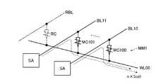
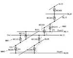
例えば、図5に示すメモリセルアレイ1において、ビット線BL11及びワード線WL00の交差部にあるメモリセルマットMM1のメモリセルMC101を選択メモリセルとする場合を考える。 For example, consider a case where in the
選択ビット線BL11に電圧Vb、選択ワード線WL00に電圧Vbよりも低い電圧Vwを印加する。ここで、電圧Vb−Vwは、メモリセルMCのアクセス動作に必要な電圧である。この時、選択ビット線BL11から選択ワード線WL00に向けて、いくつかの電流パスができる。電流パスP0は、選択メモリセルMC101を介して選択ビット線BL11から選択ワード線WL00に向かう電流パスである。この電流パスP0によって、選択メモリセルMC101には、電圧Vb−Vw程度の順方向バイアスがかかる。電流パスP1は、非選択メモリセルMC111、MC011及びMC001を介して選択ビット線BL11から選択ワード線WL00に向かう最短電流パスである。この電流パスP1によって、メモリセルMC011には、逆方向バイアスがかかる。そのため、メモリセルMC111及びMC001には、電圧Vb−Vwよりも小さい電圧しか印加されない。また、電流パスP2は、メモリセルMC211、MC210及びMC100を介して選択ビット線BL11から選択ワード線WL00に向かう最短電流パスである。この電流パスP2によって、メモリセルMC210には、逆方向バイアスが加わる。そのため、メモリセルMC211及びMC100には、電圧Vb−Vwよりも小さい電圧しか印加されない。つまり、非選択メモリセルMCには、選択メモリセルMCに印加される電圧よりも小さい電圧しか印加されないことが保証できる。 A voltage Vb is applied to the selected bit line BL11, and a voltage Vw lower than the voltage Vb is applied to the selected word line WL00. Here, the voltage Vb−Vw is a voltage necessary for the access operation of the memory cell MC. At this time, several current paths can be made from the selected bit line BL11 to the selected word line WL00. The current path P0 is a current path from the selected bit line BL11 to the selected word line WL00 via the selected memory cell MC101. Due to the current path P0, the selected memory cell MC101 is forward-biased by about the voltage Vb-Vw. The current path P1 is the shortest current path from the selected bit line BL11 to the selected word line WL00 through the unselected memory cells MC111, MC011, and MC001. Due to this current path P1, a reverse bias is applied to the memory cell MC011. Therefore, only a voltage smaller than the voltage Vb−Vw is applied to the memory cells MC111 and MC001. The current path P2 is the shortest current path from the selected bit line BL11 to the selected word line WL00 via the memory cells MC211, MC210, and MC100. By this current path P2, a reverse bias is applied to the memory cell MC210. Therefore, only a voltage smaller than the voltage Vb−Vw is applied to the memory cells MC211 and MC100. That is, it can be guaranteed that only a voltage smaller than the voltage applied to the selected memory cell MC is applied to the unselected memory cell MC.
非選択メモリセルMCに印加される電圧は、ビット線ドライバ2´及びワード線ドライバ3´から選択ビット線BL及び選択ワード線WL間に印加された電圧が複数の非選択メモリセルMCによって分圧された電圧であり、セルアレイマットMMの場所毎に自己整合的に決まる。 The voltage applied to the unselected memory cell MC is divided by the plurality of unselected memory cells MC from the voltage applied between the selected bit line BL and the selected word line WL from the
従来のクロスポイント型のメモリセルアレイの場合、非選択メモリセルに対して一定のバイアスをかけることで、非選択メモリセルへの誤ったアクセス動作を回避していた。このアクセス方式の場合、最短電流パスの中間点が固定電圧となる。そのため、メモリセルマット内で配置された場所によっては、非選択メモリセルにかなり大きなバイアスがかかる。その結果、自己整合的な状況が破壊され、非選択メモリセルには、かなり強制的にセル電流が流されることになる。 In the case of a conventional cross-point type memory cell array, an erroneous access operation to an unselected memory cell is avoided by applying a constant bias to the unselected memory cell. In the case of this access method, the intermediate point of the shortest current path is a fixed voltage. Therefore, a considerably large bias is applied to the unselected memory cell depending on the location in the memory cell mat. As a result, the self-aligned situation is destroyed, and a cell current is forced to flow through the unselected memory cell.
その点、本実施形態の場合、非選択ビット線BL及び非選択ワード線WLをフローティング状態にする。これによって、選択ビット線BL及び選択ワード線WLに印加される電圧のみ固定条件として、この条件の中で、メモリセルアレイ1は、非選択メモリセルMCに流れる総セル電流が最低になるような電圧分布に自己整合的に落ち着く。その結果、アクセス動作時のメモリセルアレイ1の消費電流を従来の半導体記憶装置に比べて小さくすることができる。 In this regard, in the present embodiment, the unselected bit line BL and the unselected word line WL are brought into a floating state. As a result, only the voltages applied to the selected bit line BL and the selected word line WL are fixed conditions. Under this condition, the
以下では、本実施形態のアクセス動作の方式を「フローティングアクセス方式」と呼ぶ。 Hereinafter, the access operation method of this embodiment is referred to as a “floating access method”.
<メモリセルに対するアクセス手順>
次に、フローティングアクセス方式によるメモリセルMCへのアクセス手順について説明する。ここでは、簡単な例として、3×3のメモリセルマットMMを積層させたメモリセルアレイ1を対象とし、メモリセルマットMM1のビット線BL11及びワード線WL01の交差部に設けられたメモリセルMC111にアクセスする場合について説明する。<Procedure for accessing memory cells>
Next, a procedure for accessing the memory cell MC by the floating access method will be described. Here, as a simple example, the target is a
図6は、メモリセルMCにアクセスする前の状態、即ち、メモリセルMCの抵抗状態が保持されている状態のメモリセルアレイ1のバイアス状態を示す図である。以下において、この状態を「スタンバイ(Stand−by)状態」と呼ぶ。 FIG. 6 is a diagram showing a bias state of the
スタンバイ状態では、全てのビット線BL及びワード線WLを接地電圧程度の電圧Vs(第1電圧又は第4電圧)に設定する。スタンバイ状態では、メモリセルMCの抵抗状態は維持されるため、メモリセルアレイ1のデータは固定される。また、スタンバイ状態では、いずれのメモリセルMCにもバイアスはかからない。 In the standby state, all the bit lines BL and word lines WL are set to a voltage Vs (first voltage or fourth voltage) that is about the ground voltage. In the standby state, the resistance state of the memory cell MC is maintained, so that the data in the
図7は、メモリセルMCにアクセスする直前の状態のメモリセルアレイ1のバイアス状態を示す図である。以下において、この状態を、「アクティブ・スタンバイ(Active stand−by)状態」と呼ぶ。 FIG. 7 is a diagram showing a bias state of the
アクティブ・スタンバイ状態では、メモリセルアレイ1の全てのビット線BL及びワード線WLを所定の電圧V(第2電圧又は第5電圧)に設定する。この電圧Vは、書き込み動作(セット動作及びリセット動作)及び読み出し動作で異なる値を取る。書き込み動作の場合、電圧Vは、セット電圧Vset、リセット電圧Vreset、或いはそれらに近い電圧Vdの半分程度にあたる電圧(〜Vset/2、〜Vreset/2、或いは〜Vd/2)となる。一方、読み出し動作の場合、電圧Vは、アクセス電圧Vaccと同程度の電圧となる。なお、アクセス電圧Vaccは、読み出し動作時に選択ビット線BLに設定する電圧であり、セット電圧Vset及びリセット電圧Vresetよりも小さく、メモリセルMCの状態が遷移しない程度の電圧である。このアクティブ・スタンバイ状態でも、スタンバイ状態と同様、いずれのメモリセルMCにもバイアスはかからない。 In the active / standby state, all the bit lines BL and word lines WL of the
なお、アクティブ・スタンバイ状態で全てのビット線BL及びワード線WLに設定される電圧Vは、後述のアクセス状態においてビット線BL或いはワード線WLに設定される最大電圧以下であれば良いため、センスアンプSAにとって適切な値の電圧とすることができる。例えば、読み出し動作の場合V=〜Vacc/2にしたり、書き込み動作の場合V=Vdにしたりすることで、セル電流が安定する時間とセンスアンプSAの作動のマッチングを図ることができる。また、選択ビット線、非選択ビット線、選択ワード線、非選択ワード線でそれぞれ異なった、最適な電圧を設定してもよい。 Note that the voltage V set for all the bit lines BL and word lines WL in the active / standby state may be equal to or lower than the maximum voltage set for the bit lines BL or word lines WL in the access state described later. The voltage can be set to an appropriate value for the amplifier SA. For example, by setting V = ˜Vacc / 2 in the read operation or V = Vd in the write operation, it is possible to match the time during which the cell current is stabilized and the operation of the sense amplifier SA. Different optimum voltages may be set for the selected bit line, the non-selected bit line, the selected word line, and the non-selected word line.
図8は、メモリセルMCから実際にデータを読み出す状態のメモリセルアレイ1のバイアス状態を示す図である。以下では、この状態の他、後述する実際にメモリセルMCをセット状態に遷移させる状態、並びに、実際にメモリセルMCをリセット状態に遷移させる状態を「アクセス状態」と呼ぶ。したがって、アクセス動作は、スタンバイ状態、アクティブ・スタンバイ状態及びアクセス状態の3つの状態で構成される。 FIG. 8 is a diagram showing a bias state of the
読み出し動作(第1アクセス動作)のアクセス状態では、選択ビット線BLにアクセス電圧Vacc(第3電圧)、選択ワード線WL01に電圧Vsを印加する一方、非選択ビット線BL及び非選択ワード線WLをフローティング状態にする。図8では、フローティング状態のビット線BL及びワード線WLの電圧をV〜で表わしている。 In the access state of the read operation (first access operation), the access voltage Vacc (third voltage) is applied to the selected bit line BL and the voltage Vs is applied to the selected word line WL01, while the unselected bit line BL and the unselected word line WL are applied. To float. In FIG. 8, voltages of the bit line BL and the word line WL in a floating state are represented by V˜.
この場合、アクティブ・スタンバイ状態において全てのビット線BL及びワード線WLが予め電圧V=Vaccに設定されているため、選択ビット線BL11からフローティング状態の非選択ビット線BL及び非選択ワード線WLに対して充電されることはない。そのため、選択ビット線BL11には、選択メモリセルMC111のデータに応じたセル電流が素早く現れる。この選択ビット線BL11に流れるセル電流をセンスアンプSAで検知することで選択メモリセルMC111の状態(セット状態又はリセット状態)を判定することができる。メモリセルMCのセット状態、リセット状態は、それぞれ‘0’、‘1’に対応しているため、メモリセルMCの状態を判定すれば選択メモリセルMC111の記憶データを読み出すことができる。 In this case, since all the bit lines BL and word lines WL are set to the voltage V = Vacc in advance in the active standby state, the selected bit line BL11 is changed to the unselected bit line BL and the unselected word line WL in the floating state. It is never charged. Therefore, a cell current corresponding to the data of the selected memory cell MC111 quickly appears on the selected bit line BL11. The state (set state or reset state) of the selected memory cell MC111 can be determined by detecting the cell current flowing through the selected bit line BL11 with the sense amplifier SA. Since the set state and the reset state of the memory cell MC correspond to “0” and “1”, respectively, the storage data of the selected memory cell MC111 can be read by determining the state of the memory cell MC.
フローティング状態(電圧V〜)のビット線BL及びワード線WLの電圧は、メモリセルアレイ1におけるメモリセルMCの配置場所に応じて自己整合的に所定の電圧に落ち着くが、その過程において、非選択メモリセルMCにも電流が流れる。この非選択メモリセルMCに流れる電流は、大別して間接順方向電流、間接逆方向電流に分類することができる。最短電流パスを流れる電流が途中の非選択メモリセルを順方向に通過する場合、この非選択メモリセルを「間接順方向電流が流れるメモリセル」と言い、最短電流パスを流れる電流が途中の非選択メモリセルを逆方向に通過する場合、この非選択メモリセルを「間接逆方向電流が流れるメモリセル」と言う。図8では、選択メモリセルMCの流れるセル電流を白抜き矢印、間接順方向電流が流れる非選択メモリセルMCを実線矢印、間接逆方向電流が流れる非選択メモリセルMCを点線矢印でそれぞれ示している。白抜き矢印、実線矢印及び点線矢印は、いずれも電流が流れる向きも示している。 The voltage of the bit line BL and the word line WL in the floating state (voltage V˜) settles to a predetermined voltage in a self-aligned manner in accordance with the arrangement location of the memory cell MC in the
例えば、非選択メモリセルMC101、MC100及びMC110を介して選択ビット線BL11から選択ワード線WL01に向かう最短電流パスP0について見ると、非選択メモリセルMC101及びMC110に間接順方向電流が流れ、非選択メモリセルMC100に間接逆方向電流が流れることになる。 For example, when looking at the shortest current path P0 from the selected bit line BL11 to the selected word line WL01 via the non-selected memory cells MC101, MC100, and MC110, an indirect forward current flows through the non-selected memory cells MC101 and MC110. An indirect reverse current flows through the memory cell MC100.
つまり、選択ビット線BL11又は選択ワード線WL01に接続された非選択メモリセルMCに間接順方向電流が流れ、これら間接順方向電流が流れるメモリセルと同じ非選択ビット線BL又は非選択ワード線WLに接続された非選択メモリセルMCに間接逆方向電流が流れることが分かる。また、間接順方向電流又は間接逆方向電流が流れる非選択メモリセルMCは、選択メモリセルMC111が属するメモリセルマットMM1並びに、このメモリセルマットMM1の上下に隣接するメモリセルマットMM0及びMM2の範囲にのみ存在し、メモリセルマットMM1に隣接しないメモリセルマットMM3には存在しないことが分かる。 That is, an indirect forward current flows through unselected memory cells MC connected to the selected bit line BL11 or selected word line WL01, and the same unselected bit line BL or unselected word line WL as the memory cell through which these indirect forward current flows. It can be seen that an indirect reverse current flows through the non-selected memory cells MC connected to. Further, the non-selected memory cell MC through which the indirect forward current or the indirect reverse current flows is the range of the memory cell mat MM1 to which the selected memory cell MC111 belongs and the memory cell mats MM0 and MM2 adjacent above and below this memory cell mat MM1. It can be seen that the memory cell mat MM3 that is not adjacent to the memory cell mat MM1 does not exist.
図9は、メモリセルMCのセット動作(第1アクセス動作)のアクセス状態のメモリセルアレイ1のバイアス状態を示す図である。 FIG. 9 is a diagram illustrating a bias state of the
セット動作のアクセス状態では、選択ビット線BL11にセット電圧Vset(第3電圧)、選択ワード線WL01に電圧Vsを印加する一方、非選択ビット線BL及び非選択ワード線WLはフローティング状態とする。 In the access state of the set operation, the set voltage Vset (third voltage) is applied to the selected bit line BL11 and the voltage Vs is applied to the selected word line WL01, while the unselected bit line BL and the unselected word line WL are in a floating state.
この場合、アクティブ・スタンバイ状態において全てのビット線BL及びワード線WLが予め電圧V=〜Vset/2に設定されているため、放電電流が選択ワード線WL01に集中せず、充電電流として選択ビット線BL11にも供給される。また、ビット線ドライバ2´から遠く、ワード線ドライバ3´に近い場所の非選択メモリセルMCに対して、過渡的にでもセット電圧Vsetに近い電圧が印加されるのを防ぐことができる。 In this case, since all the bit lines BL and word lines WL are set to the voltage V = ˜Vset / 2 in advance in the active standby state, the discharge current is not concentrated on the selected word line WL01, and the selected bit is used as the charging current. It is also supplied to the line BL11. Further, it is possible to prevent a voltage close to the set voltage Vset from being applied to the non-selected memory cells MC located far from the
フローティング状態(電圧V〜)のビット線BL及びワード線WLは、メモリセルアレイ1におけるメモリセルMCの位置によって自己整合的に所定の電圧に落ち着くが、その過程において、非選択メモリセルMCにも電流が流れる点については、読み出し動作のアクセス状態と同じである。但し、電圧Vの値が異なるため、メモリセルアレイ1のバイアス状態と電流の過渡的な変化は異なる。 The bit line BL and the word line WL in the floating state (voltage V˜) settle to a predetermined voltage in a self-aligned manner depending on the position of the memory cell MC in the
図10は、メモリセルMCのリセット動作(第2アクセス動作)のアクセス状態のメモリセルアレイ1のバイアス状態を示す図である。 FIG. 10 is a diagram showing a bias state of the
リセット動作のアクセス状態では、選択ビット線BL11に電圧Vs、選択ワード線WL01にリセット電圧Vreset(第6電圧)を印加する。これは、セット動作時と逆のバイアス状態である。一方、非選択ビット線BL及び非選択ワード線WLはフローティング状態とする。 In the access state of the reset operation, the voltage Vs is applied to the selected bit line BL11, and the reset voltage Vreset (sixth voltage) is applied to the selected word line WL01. This is a bias state opposite to that in the set operation. On the other hand, the unselected bit line BL and the unselected word line WL are set in a floating state.
この場合、アクティブ・スタンバイ状態において全てのビット線BL及びワード線WLが予め電圧V=〜Vreset/2に設定されているため、放電電流が選択ビット線BL11に集中せず、充電電流として選択ワード線WL01にも供給される。また、ワード線ドライバ3´から遠く、ビット線ドライバ2´に近い場所の非選択メモリセルMCに対して、過渡的にでもリセット電圧Vresetに近い電圧が印加されるのを防ぐことができる。 In this case, since all the bit lines BL and word lines WL are set in advance to the voltage V = ˜Vreset / 2 in the active standby state, the discharge current is not concentrated on the selected bit line BL11, and the selected word is used as the charging current. It is also supplied to the line WL01. Further, it is possible to prevent a voltage close to the reset voltage Vreset from being applied to the non-selected memory cells MC located far from the
フローティング状態(電圧V〜)のビット線BL及びワード線WLは、メモリセルアレイ1におけるメモリセルMCの位置によって自己整合的に所定の電圧に落ち着くが、その過程において、非選択メモリセルMCにも電流が流れる点については、読み出し動作及びセット動作のアクセス状態と同じである。但し、選択メモリセルMC111を逆方向バイアスの状態にするため、間接順方向電流が流れる非選択メモリセルMCと間接逆方電流が流れる非選択メモリセルMCが、読み出し動作やセット動作のアクセス状態と全く逆になる。 The bit line BL and the word line WL in the floating state (voltage V˜) settle to a predetermined voltage in a self-aligned manner depending on the position of the memory cell MC in the
以上説明したフローティングアクセス方式を用いた場合、メモリセルアレイ1に欠陥が発生さいた場合にも容易に対応することができる。次に、この点について、説明する。 When the floating access method described above is used, it is possible to easily cope with a case where a defect occurs in the
従来の半導体記憶装置では、不良メモリセルがある場合、他のメモリセルへのアクセスの影響を考慮し、当該不良メモリセルをスペアのメモリセルに置き換えるか、或いは、不良メモリセルをメモリセルアレイから回路的に切り離すなどの措置によって対応していた。 In the conventional semiconductor memory device, when there is a defective memory cell, the influence of access to other memory cells is taken into consideration, and the defective memory cell is replaced with a spare memory cell, or the defective memory cell is replaced with a circuit from the memory cell array. We responded by measures such as detaching.
その点、本実施形態のフローティングアクセス方式の場合、不良メモリセルによってこの不良メモリセルに接続されているビット線BLやワード線WLが短絡している場合であっても、スタンバイ状態やアクティブ・スタンバイ状態では、これらビット線BL及びワード線WL間には電位差が生じないため問題とならない。また、アクセス状態では、選択メモリセルMC以外は、フローティング状態であり、欠陥の影響はメモリセルアレイ1内の抵抗分布の変化として現れるため、欠陥発生部位を含む領域から離れたメモリセルMCにアクセスする限りにおいては影響を無視できる。即ち、読み出し動作時や書き込み動作時に、異常電流が流れたり誤動作をしたりする領域をアドレス管理によってアクセス禁止領域とするだけで足りる。 In this regard, in the case of the floating access method of this embodiment, even when the bit line BL or the word line WL connected to the defective memory cell is short-circuited by the defective memory cell, the standby state or active standby In this state, there is no problem because no potential difference is generated between the bit line BL and the word line WL. In the access state, except for the selected memory cell MC, it is in a floating state, and the influence of the defect appears as a change in the resistance distribution in the
これは磁気ディスクや光ディスクにおいて欠陥が存在する領域を使用しない事に似ており、メモリ素子として特別な対応をしないことに似ている。勿論、メモリ素子として内部にアクセスできないようなアドレスの情報を持たせることもできるが、メモリセルアレイの回路システムによってリダンダンシなどを用いた対応をとる必要は無く、アドレスの管理だけで対応することができる。 This is similar to not using a defect-existing area in a magnetic disk or an optical disk, and similar to not taking any special measures as a memory element. Of course, it is possible to have address information that cannot be accessed internally as a memory element, but it is not necessary to take a response using redundancy or the like depending on the circuit system of the memory cell array, and it can be handled only by address management. .
例えば、メモリセルアレイ1の所定の部位に欠陥が生じたとする。この時、最悪の場合、図11に示すように、この欠陥発生部位を中心としてビット線BL方向及びワード線WL方向に十字状にアクセス禁止領域が発生する。欠陥の種類によっては、このアクセス禁止領域内であっても、正常にアクセスできる箇所も存在するが、アクセスして不良が生じるか否かに依存するため、実使用状態でアドレスが管理されることになる。 For example, it is assumed that a defect occurs in a predetermined part of the
<まとめ>
以上、本実施形態によれば、アクセス動作時に、選択メモリセル以外をフローティング状態にする。そのため、消費電力を小さくすることができる。また、フローティング状態を作り出すだけなので、配線ドライバ等の周辺回路も小さいスペースに実装可能である。更に、メモリセルアレイに欠陥が生じた場合、それを補償する特別な回路を必要とせず、アドレス管理だけで対応することができるため、大容量ファイルメモリに向いた半導体記憶装置を提供することができる。<Summary>
As described above, according to the present embodiment, other than the selected memory cell is set in a floating state during an access operation. Therefore, power consumption can be reduced. Further, since only a floating state is created, peripheral circuits such as wiring drivers can be mounted in a small space. Further, when a defect occurs in the memory cell array, a special circuit for compensating for the defect can be dealt with only by address management, so that a semiconductor memory device suitable for a large capacity file memory can be provided. .
[第2の実施形態]
第1の実施形態では、1つのメモリセルMCにアクセスする場合について説明したが、第2の実施形態では、複数のメモリセルMCに同時にアクセスする場合について説明する。[Second Embodiment]
In the first embodiment, a case where one memory cell MC is accessed has been described. In the second embodiment, a case where a plurality of memory cells MC are accessed simultaneously will be described.
先ず、複数のメモリセルMCに同時に読み出す動作する場合について説明する。
図3に示した非対称抵抗変化メモリセル(メモリセルMC)は、大電流が流れ続けるとその特性が変化してしまう。そのため、セル電流をモニタするビット線BLについては、1本毎に1つのメモリセルMCを選択するようにして、メモリセルMC毎にセル電流をモニタして、制御できるようにする必要がある。First, a description will be given of the case where the read operation is performed simultaneously on a plurality of memory cells MC.
The characteristics of the asymmetric resistance change memory cell (memory cell MC) shown in FIG. 3 change when a large current continues to flow. For this reason, it is necessary to select one memory cell MC for each bit line BL for monitoring the cell current so that the cell current can be monitored and controlled for each memory cell MC.
そこで、本実施形態では、同時に複数のメモリセルMCにアクセスする際、ワード線WLを1本だけ選択し、ビット線BLを複数選択する。選択ワード線WLとワード線ドライバ3´との距離を短くして、選択ワード線WLの許容電流内においてできるだけ多くのビット線BLを選択する。 Therefore, in this embodiment, when accessing a plurality of memory cells MC at the same time, only one word line WL is selected and a plurality of bit lines BL are selected. The distance between the selected word line WL and the word line driver 3 'is shortened, and as many bit lines BL as possible are selected within the allowable current of the selected word line WL.
選択ビット線BLに流れるセル電流Icellの大小を検知するには、この選択ビット線BLと同一環境の参照ビット線RBLが必要になる。読み出し動作においては、最低でもビット線BLと参照ビット線BLBの2本のビット線をドライブし、参照ビット線RBLに流れる電流と選択ビット線BLに流れるセル電流Icellとを選択ビット線BLの一端に設けられたセンスアンプSAで比較する。この比較によって、選択メモリセルMCの抵抗状態、つまり選択メモリセルMCが記憶するデータを判定することができる。
次に、複数のメモリセルMCに同時にセット動作する場合について説明する。In order to detect the magnitude of the cell current Icell flowing through the selected bit line BL, the reference bit line RBL having the same environment as the selected bit line BL is required. In the read operation, at least two bit lines of the bit line BL and the reference bit line BLB are driven, and a current flowing through the reference bit line RBL and a cell current Icell flowing through the selected bit line BL are connected to one end of the selected bit line BL. The comparison is made with the sense amplifier SA provided in FIG. By this comparison, the resistance state of the selected memory cell MC, that is, the data stored in the selected memory cell MC can be determined.
Next, a case where a set operation is simultaneously performed on a plurality of memory cells MC will be described.
セット動作の場合、1本の選択ワード線WLに電圧Vsを印加し、複数の選択ビット線BLにセット電圧Vsetを印加し、非選択ビット線BL及び非選択ワード線WLをフローティング状態にする。 In the set operation, the voltage Vs is applied to one selected word line WL, the set voltage Vset is applied to a plurality of selected bit lines BL, and the unselected bit lines BL and the unselected word lines WL are brought into a floating state.
なお、このセット動作の際、センスアンプSAを利用することができる。選択ビット線BLに接続されたセンスアンプSAは、上記の通り、セル電流をモニタする役割を持っている。そこで、センスアンプSAによって、セット動作中の選択メモリセルMCのセル電流Icellをモニタする。そして、センスアンプSAが、リセット状態(高抵抗状態)からセット状態(低抵抗状態)に遷移した時のセル電流Icellの増加を検知した時点で、ビット線ドライバ2´からそのビット線BLを切り離すようにする。これによって、選択メモリセルMCに余分な電流が流れず、当該選択メモリセルMCの特性の変化を防ぐことができる。これは、各々の選択ビット線BLに流れるセル電流IcellをセンスアンプSAで個別にモニタすることで可能になる。 In this setting operation, the sense amplifier SA can be used. As described above, the sense amplifier SA connected to the selected bit line BL has a role of monitoring the cell current. Therefore, the cell current Icell of the selected memory cell MC during the set operation is monitored by the sense amplifier SA. When the sense amplifier SA detects an increase in the cell current Icell when the reset state (high resistance state) transitions to the set state (low resistance state), the bit line BL is disconnected from the bit line driver 2 '. Like that. As a result, no excess current flows through the selected memory cell MC, and changes in the characteristics of the selected memory cell MC can be prevented. This can be achieved by individually monitoring the cell current Icell flowing through each selected bit line BL with the sense amplifier SA.
次に、複数の選択メモリセルMCに同時にリセット動作する場合について説明する。 Next, a case where a reset operation is simultaneously performed on a plurality of selected memory cells MC will be described.
リセット動作の場合、1本の選択ワード線WLにリセット電圧Vresetを印加し、複数の選択ビット線BLに電圧Vsを印加し、非選択ビット線BL及び非選択ワード線WLをフローティング状態にする。 In the reset operation, the reset voltage Vreset is applied to one selected word line WL, the voltage Vs is applied to a plurality of selected bit lines BL, and the unselected bit lines BL and the unselected word lines WL are brought into a floating state.
リセット動作の場合、選択メモリセルMCには逆方向バイアスがかかるが、この場合、図3中(B)を用いて説明したように、非対称抵抗変化メモリセルの特性上、セル電流は非常に小さい。そのため、ビット線BLの選択方法は重要とはならない。したがって、セット動作に用いる選択デコーダをそのまま流用し、セット動作時と同じ方法によってビット線BLを選択することもできる。 In the reset operation, a reverse bias is applied to the selected memory cell MC. In this case, as described with reference to FIG. 3B, the cell current is very small due to the characteristics of the asymmetric resistance change memory cell. . Therefore, the selection method of the bit line BL is not important. Therefore, the selection decoder used for the set operation can be used as it is, and the bit line BL can be selected by the same method as in the set operation.
なお、読み出し動作、セット動作及びリセット動作のいずれの動作においても、ビット線BLには、メモリセルMC1つ分のセル電流Icellしか流れない。そのため、ビット線BLは、ワード線WLに比べて長くても問題はない。一方、ワード線WLは、参照ビット線RBLも含め複数のビット線BLを同時にドライブすることになる。そのため、参照ビット線RBLも含めn本のビット線BLを選択する場合、ワード線WLは、n×Icellの電流を許容できるものでなければならない。 Note that, in any of the read operation, the set operation, and the reset operation, only the cell current Icell corresponding to one memory cell MC flows through the bit line BL. Therefore, there is no problem even if the bit line BL is longer than the word line WL. On the other hand, the word line WL simultaneously drives a plurality of bit lines BL including the reference bit line RBL. For this reason, when selecting n bit lines BL including the reference bit line RBL, the word line WL must be capable of accepting a current of n × Icell.
また、選択される複数のビット線BLは、同一のワード線WLに接続されたメモリセルMCに接続されているものであれば良い。 Further, the selected bit lines BL may be connected to the memory cells MC connected to the same word line WL.
図12〜図14は、本実施形態に係るビット線BLの選択例である。図12〜図14中点線で示されたメモリセル、ビット線は、それぞれ参照セルRC、参照ビット線RBLを示す。 12 to 14 are examples of selection of the bit line BL according to this embodiment. The memory cells and bit lines indicated by dotted lines in FIGS. 12 to 14 indicate reference cells RC and reference bit lines RBL, respectively.
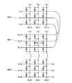
図12は、同一のメモリセルマットMMから複数のメモリセルMCを選択する例である。ワード線WL00と、ビット線BL10及びBL11を選択することで、メモリセルマットMM1の2つのメモリセルMC100及びMC101に同時にアクセスすることができる。 FIG. 12 shows an example in which a plurality of memory cells MC are selected from the same memory cell mat MM. By selecting the word line WL00 and the bit lines BL10 and BL11, the two memory cells MC100 and MC101 of the memory cell mat MM1 can be accessed simultaneously.
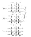
図13は、上下に隣接し且つ1つのワード線WLを共有する2つのメモリセルマットMMから複数のメモリセルMCを選択する例である。ワード線WL01と、ビット線BL00及びBL11を選択することで、メモリセルマットMM0のメモリセルMC000及びメモリセルマットMM1のメモリセルMC101に同時にアクセスすることができる。 FIG. 13 shows an example in which a plurality of memory cells MC are selected from two memory cell mats MM that are vertically adjacent and share one word line WL. By selecting the word line WL01 and the bit lines BL00 and BL11, the memory cell MC000 of the memory cell mat MM0 and the memory cell MC101 of the memory cell mat MM1 can be accessed simultaneously.
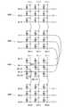
図14も、図13と同様、上下に隣接し且つ1つのワード線WLを共有する2つのメモリセルマットMMから複数のメモリセルMCを選択する例である。図14の場合、図13とは異なり、同じビット線グループに属するビット線BL01及びBL11を選択している。これによって、メモリセルマットMM0のメモリセルMC001及びメモリセルマットMM1のメモリセルMC101に同時にアクセスできる。 FIG. 14 is also an example in which a plurality of memory cells MC are selected from two memory cell mats MM that are adjacent vertically and share one word line WL, as in FIG. In the case of FIG. 14, unlike FIG. 13, bit lines BL01 and BL11 belonging to the same bit line group are selected. As a result, the memory cell MC001 of the memory cell mat MM0 and the memory cell MC101 of the memory cell mat MM1 can be accessed simultaneously.
図12〜図14に示した例の他、同じワード線WLを共有するメモリセルマットMMの範囲であれば、ワード線WLの許容電流の範囲内において、複数のビット線BLを任意に選択することができる。 In addition to the examples shown in FIGS. 12 to 14, in the range of the memory cell mat MM sharing the same word line WL, a plurality of bit lines BL are arbitrarily selected within the allowable current range of the word line WL. be able to.
以上、本実施形態によれば、第1の実施形態と同様の効果を得られるばかりでなく、複数のメモリセルに同時にアクセスできるため、アクセス動作の処理時間を短縮することができる。 As described above, according to the present embodiment, not only the same effects as those of the first embodiment can be obtained, but also a plurality of memory cells can be accessed simultaneously, so that the processing time of the access operation can be shortened.
[第3の実施形態]
第3の実施形態では、異なるメモリセルから連続してデータを読み出す方法について説明する。以下において、この方法による読み出し動作を「連続読み出し動作」と呼ぶ。[Third Embodiment]
In the third embodiment, a method of reading data continuously from different memory cells will be described. Hereinafter, the read operation by this method is referred to as “continuous read operation”.
連続読み出し動作の方法には2つ考えられる。1つ目は、選択ワード線を固定してビット線をアクセスサイクル毎に順次切り換えて選択する方法である。2つ目は、選択ビット線を固定してワード線をアクセスサイクル毎に順次切り換えて選択する方法である。これら方法のうち、フローティングアクセス方式の場合、2つ目の方法が有利である。 There are two possible methods for the continuous reading operation. The first is a method in which the selected word line is fixed and the bit lines are sequentially switched and selected every access cycle. The second is a method in which the selected bit line is fixed and the word lines are sequentially switched and selected every access cycle. Of these methods, the second method is advantageous for the floating access method.
図15は、本実施形態に係る半導体記憶装置における連続読み出し動作を説明する図であり、図16は、本実施形態のフローティングアクセス方式を用いてメモリセルに1回アクセスした場合のビット線の電圧変化を示す図である。 FIG. 15 is a diagram for explaining the continuous read operation in the semiconductor memory device according to this embodiment. FIG. 16 shows the voltage of the bit line when the memory cell is accessed once using the floating access method of this embodiment. It is a figure which shows a change.
読み出し動作では、第1の実施形態でも説明したように、アクティブ・スタンバイ状態において、全てのビット線BL及びワード線WLにアクセス電圧Vaccを印加させた後、アクセス状態において、選択ビット線BLにアクセス電圧Vaccを印加し、選択ワード線WLに電圧Vsを印加し、非選択ビット線BL及び非選択ワード線WLをフローティング状態にする。 In the read operation, as described in the first embodiment, after the access voltage Vacc is applied to all the bit lines BL and the word lines WL in the active standby state, the selected bit line BL is accessed in the access state. The voltage Vacc is applied, the voltage Vs is applied to the selected word line WL, and the unselected bit line BL and the unselected word line WL are brought into a floating state.
この場合、図16に示すように、選択ビット線BLの電圧Vbは、時刻t0のアクセス動作開始時のアクセス電圧Vaccからほとんど変化しない。一方、非選択ビット線の電圧Vbは、ビット線BL毎にばらつきはあるもの、電圧Vsに向かって下がるため、アクセス電圧Vaccよりもかなり低くなる。 In this case, as shown in FIG. 16, the voltage Vb of the selected bit line BL hardly changes from the access voltage Vacc at the start of the access operation at time t0. On the other hand, the voltage Vb of the non-selected bit line is considerably lower than the access voltage Vacc because it varies toward the voltage Vs although there is variation for each bit line BL.
そのため、2つ目の方法のように、ビット線BLの電圧Vbを変化させずに固定しておき、メモリセルアレイ1のバイアス状態の変化を少なくする方が、連続読み出し動作を高速に行うことができる。 Therefore, as in the second method, if the voltage Vb of the bit line BL is fixed without being changed and the change in the bias state of the
つまり、図15に示すように、選択ビット線BLの電圧Vbは、アクセス電圧Vacc(第7電圧)で固定させる一方、選択ワード線WLを順次切り替えて行く。選択ワード線WLは、接地電圧に近い電圧Vs(第9電圧)でドライブさせる必要があるが、フローティングアクセス方式の場合、選択ワード線WL以外はフローティング状態であるため既に電圧Vsの近くまで放電されている。そのため、ワード線WLの選択を順次切り替えてもメモリセルアレイ1のバイアス状態は大きく変化しない。 That is, as shown in FIG. 15, the voltage Vb of the selected bit line BL is fixed at the access voltage Vacc (seventh voltage), while the selected word line WL is sequentially switched. The selected word line WL needs to be driven with a voltage Vs (9th voltage) close to the ground voltage. However, in the floating access method, since the other than the selected word line WL is in a floating state, it has already been discharged to near the voltage Vs. ing. Therefore, the bias state of the
なお、連続読み出し動作の場合、センスアンプSAを、選択ワード線WLの切り換えるアクセスサイクル毎に初期化させる必要がある。 In the case of continuous read operation, it is necessary to initialize the sense amplifier SA every access cycle for switching the selected word line WL.
以上、本実施形態によれば、第1の実施形態と同様の効果を得られるばかりでなく、連続読み出し動作の際、選択ビット線を固定しつつ、選択ワード線を順次切り替える方法を用いることで、高速且つ低消費電力な連続読み出し動作をする半導体記憶装置を提供することができる。 As described above, according to the present embodiment, not only the same effects as those of the first embodiment can be obtained, but also a method of sequentially switching the selected word lines while fixing the selected bit lines in the continuous read operation can be used. It is possible to provide a semiconductor memory device that performs a continuous read operation with high speed and low power consumption.
[第4の実施形態]
第4の実施形態では、複数のワード線WLでワード線ドライバ3´を共有させた半導体記憶装置について説明する。[Fourth Embodiment]
In the fourth embodiment, a semiconductor memory device in which a word line driver 3 'is shared by a plurality of word lines WL will be described.
フローティングアクセス方式の場合、選択ビット線BLと選択ワード線WLのみを一定の電圧でドライブするが、異なるメモリセルマットMMに属するワード線WLであれば、ワード線ドライバ3´を共用することができる。 In the case of the floating access method, only the selected bit line BL and the selected word line WL are driven with a constant voltage. However, if the word line WL belongs to a different memory cell mat MM, the word line driver 3 'can be shared. .
先ず、所定のメモリセルMCにアクセスした場合にバイアス状態が変化するメモリセルアレイ1の範囲について説明しておく。 First, the range of the
選択メモリセルMCの存在する選択メモリセルマットMMの電圧の影響を受けるのは、主に、選択メモリセルマットマットMMの上下に隣接し最短電流セルが通るメモリセルマットMMである。図17に示す例では、ビット線BL01及びワード線WL10の交差部に設けられたメモリセルマットMM1のメモリセルMC101にアクセスする場合、図17中点線で示すような最短電流パスP0及びP1ができる。電流パスP0は、メモリセルマットMM1の下に隣接するメモリセルマットMM0の非選択メモリセルMC001、MC000及びメモリセルマットMM1の非選択メモリセルMC100を介して、選択ビット線BL10から選択ワード線WL10に向かうパスである。また、電流パスP1は、メモリセルマットMM1の非選択メモリセルMC111、メモリセルマットMM1の上に隣接するメモリセルマットMM2の非選択メモリセルMC210及びMC200を介して、選択ビット線BL10から選択ワード線WL10に向かうパスである。このように、メモリセルマットMM1のメモリセルMCにアクセスすると、上下に隣接する2つのメモリセルマットMM0及びMM2が主に影響が受ける範囲となることが分かる。以下では、この範囲を「電流パス範囲」と呼ぶ。なお、図17中“float*”と表わしたワード線WLは、フローティング状態を維持して自己整合的な電圧となることが必要なワード線WLである。 The memory cell mat MM that is affected by the voltage of the selected memory cell mat MM in which the selected memory cell MC exists is mainly the memory cell mat MM adjacent to the upper and lower sides of the selected memory cell mat mat MM and through which the shortest current cell passes. In the example shown in FIG. 17, when accessing the memory cell MC101 of the memory cell mat MM1 provided at the intersection of the bit line BL01 and the word line WL10, the shortest current paths P0 and P1 as shown by the dotted line in FIG. . The current path P0 passes from the selected bit line BL10 to the selected word line WL10 via the unselected memory cells MC001 and MC000 of the memory cell mat MM0 adjacent to the memory cell mat MM1 and the unselected memory cell MC100 of the memory cell mat MM1. This is the path to The current path P1 is selected from the selected bit line BL10 via the unselected memory cell MC111 of the memory cell mat MM1 and the unselected memory cells MC210 and MC200 of the memory cell mat MM2 adjacent on the memory cell mat MM1. This is a path toward the line WL10. Thus, it can be seen that when the memory cell MC of the memory cell mat MM1 is accessed, the two memory cell mats MM0 and MM2 adjacent in the vertical direction are mainly affected. Hereinafter, this range is referred to as a “current path range”. Note that the word line WL represented as “float *” in FIG. 17 is a word line WL that needs to maintain a floating state and become a self-aligned voltage.
第2の実施形態のように複数のビット線BLを選択する場合、選択メモリセルMCは、選択ワード線WLを共有する2つの選択メモリセルマットMMの範囲となる。複数のメモリセルMCに同時にアクセスする場合、選択ワード線WLの層の上下それぞれ2つのメモリセルマットMMが、主な電流パス範囲となる。 When a plurality of bit lines BL are selected as in the second embodiment, the selected memory cell MC is in a range of two selected memory cell mats MM sharing the selected word line WL. When accessing a plurality of memory cells MC simultaneously, two memory cell mats MM above and below the layer of the selected word line WL are the main current path ranges.
逆に、この主な電流パス範囲外の領域における電圧設定は、選択メモリセルMCとその周辺領域に対してほとんど影響を及ぼさない。そこで、主な電流パス範囲内の“float*”で示したワード線WLのフローティング状態を維持でき、一定の電圧に固定されないことを条件に、1つのワード線ドライバ3´によって、選択メモリセルマットMMを含む複数の選択メモリセルマットMMのワード線を同時にドライブすることができる。その結果、ワード線ドライバ3´の構成を簡単にすることができる。 On the contrary, the voltage setting in the region outside the main current path range hardly affects the selected memory cell MC and its peripheral region. Therefore, the selected memory cell mat is selected by one
本実施形態では、メモリセルマットMMの積層方向に並ぶワード線1本置きにワード線ドライバ3´を共用させる。つまり、同じワード線グループのうち、下層から数えて偶数番目にあるワード線WLと、下層から数えて奇数番目にあるワード線WLとを、それぞれ1つの組にして、各組で1つのワード線ドライバ3a´(第1ドライバ)、3b´(第2ドライバ)を共用させる。 In the present embodiment, the word line driver 3 'is shared for every other word line arranged in the stacking direction of the memory cell mats MM. That is, in the same word line group, the even-numbered word lines WL counted from the lower layer and the odd-numbered word lines WL counted from the lower layer are made into one set, and one word line in each set. The
そして、選択ワード線WLが奇数番目であれば、ワード線ドライバ3a´によって他の奇数番目のワード線WLと同時に電圧Vwでドライブし、選択ワード線WLが偶数番目であれば、ワード線ドライバ3b´によって他の偶数番目のワード線WLと同時に電圧Vwでドライブする。このようなワード線WLのドライブ方式によって、主な電流パス範囲のバイアス状態を維持することができる。 If the selected word line WL is odd-numbered, the
図18及び図19は、本実施形態において、所定のメモリセルMCにアクセスした場合のメモリセルアレイ1のバイアス状態を示す図である。図18は、奇数番目のワード線WLを選択した場合、図19は、偶数番目のワード線WLを選択した場合になる。図中、“float*”は、図17と同様、フローティング状態を維持して自己整合的な電圧になることが必要なワード線WLを示している。 18 and 19 are diagrams showing the bias state of the
ワード線WLは、下層から上層に掛けてWL00、WL01〜WL80、WL81まで積層されている。このうち、奇数番目のワード線WL10、WL30、WL50及びWL70が、図18に示すように、1つのワード線ドライバ3a´を共用している。また、偶数番目のワード線WL00、WL20、WL40、WL60及びWL80が、図19に示すように、1つのワード線ドライバ3b´を共用している。 The word lines WL are stacked from the lower layer to the upper layer from WL00, WL01 to WL80, WL81. Among these, odd-numbered word lines WL10, WL30, WL50 and WL70 share one
メモリセルマットMM5のメモリセルMC500及びメモリセルマットMM6のメモリセルMC600を選択する場合、図18に示すように、メモリセルマットMM5の下に隣接するメモリセルマットMM4からメモリセルマットMM6の上に隣接するメモリセルマットMM7までが主な電流パス範囲となる。この場合、奇数番目のワード線WLに対してワード線ドライバ3a´から電圧Vwを印加する一方、偶数番目のワード線WLをフローティング状態にする。これによって、電流パス範囲内では、選択ワード線WL30に電圧Vwが印加され、非選択ワード線WLがフローティング状態になる。その結果、非選択メモリセルMCには、余計な電圧が印加されず、選択メモリセルMC500及びMC600に対してのみアクセス動作することができる。 When the memory cell MC500 of the memory cell mat MM5 and the memory cell MC600 of the memory cell mat MM6 are selected, as shown in FIG. 18, from the memory cell mat MM4 adjacent to the memory cell mat MM5 to above the memory cell mat MM6. The main current path range is up to the adjacent memory cell mat MM7. In this case, the voltage Vw is applied from the
メモリセルマットMM7のメモリセルMC700及びメモリセルマットMM8のメモリセルMC800を選択する場合、図19に示すように、メモリセルマットMM7の下に隣接するメモリセルマットMM6からメモリセルマットMM8の上に隣接するメモリセルマットMM9までが主な電流パス範囲となる。この場合、偶数番目のワード線WLに対してワード線ドライバ3b´から電圧Vwを印加する一方、奇数番目のワード線WLをフローティング状態にする。これによって、電流パス範囲内では、選択ワード線WL40に電圧Vwが印加さえ、非選択ワード線WLがフローティング状態になる。その結果、非選択メモリセルMCには、余計な電圧が印加されず、選択メモリセルMC500及びMC600に対してのみアクセス動作することができる。 When selecting the memory cell MC700 of the memory cell mat MM7 and the memory cell MC800 of the memory cell mat MM8, as shown in FIG. 19, from the memory cell mat MM6 adjacent to the memory cell mat MM7 to above the memory cell mat MM8. The main current path range is up to the adjacent memory cell mat MM9. In this case, the voltage Vw is applied from the word line driver 3b ′ to the even-numbered word lines WL, while the odd-numbered word lines WL are brought into a floating state. As a result, in the current path range, even if the voltage Vw is applied to the selected word line WL40, the unselected word line WL is in a floating state. As a result, no extra voltage is applied to the unselected memory cells MC, and only the selected memory cells MC500 and MC600 can be accessed.
以上、本実施形態によれば、第1の実施形態と同様の効果を得られるばかりでなく、ワード線ドライバ3´を複数のメモリセルマットMMに共用できるため、ロウ制御回路3の回路規模を小さくでき、延いては、チップサイズが小さい半導体記憶装置を提供することができる。 As described above, according to the present embodiment, not only the same effects as in the first embodiment can be obtained, but also the
[第5の実施形態]
第5の実施形態では、メモリセルマットMMが複数積層されたメモリセルアレイ1を備える半導体記憶装置のカラム制御回路2及びロウ制御回路3の構成に関する実施形態について説明する。[Fifth Embodiment]
In the fifth embodiment, an embodiment relating to the configuration of the
各メモリセルマットMMのワード線WL毎に個別にワード線ドライバ3´を設けることはチップサイズの点で不利である。そこで、本実施形態に係る半導体装置は、所定数のワード線グループからなるワード線ブロック毎に1つのワード線ドライバ3´で共用するように構成する。 Providing the word line driver 3 'individually for each word line WL of each memory cell mat MM is disadvantageous in terms of chip size. Therefore, the semiconductor device according to the present embodiment is configured to be shared by one word line driver 3 'for each word line block composed of a predetermined number of word line groups.
図20は、本実施形態に係る半導体記憶装置のロウ制御回路3の構成を示す図である。ロウ制御回路3は、ワード線ドライバ3´の他、メモリセルマット選択回路、メモリセルマット内位置選択回路、配線ブロック選択回路を有する。 FIG. 20 is a diagram showing a configuration of the
配線ブロック選択回路は、1つのワード線ブロック毎に1つ備わっている。この配線ブロック選択回路は、メモリセルアレイ1のうち選択ワード線WLが属するワード線ブロックを選択する回路である。 One wiring block selection circuit is provided for each word line block. The wiring block selection circuit is a circuit that selects a word line block to which the selected word line WL belongs in the
メモリセルマット内位置選択回路は、1つのワード線ブロック毎に1つ備わっている。このメモリセルマット内位置選択回路は、メモリセルマットMM内の選択ワード線WLの位置を選択する回路である。換言、配線ブロック選択回路が選択したワード線ブロックのうち選択ワード線WLが属するワード線グループを選択する回路と言える。 One memory cell mat position selection circuit is provided for each word line block. The memory cell mat position selection circuit is a circuit that selects the position of the selected word line WL in the memory cell mat MM. In other words, it can be said that the word line block to which the selected word line WL belongs is selected from the word line blocks selected by the wiring block selection circuit.
メモリセルマット選択回路は、1つのワード線グループ毎に1つ備わっている。このメモリセルマット選択回路は、配線ブロック選択回路が選択したワード線ブロックのうち選択ワード線WLが属するメモリセルマットMMを選択する回路である。なお、第4の実施形態のように、ワード線グループを奇数番目のワード線の組と、偶数番目のワード線の組でまとめてドライブする場合、メモリセルマット選択回路は、二分岐の選択回路となる。 One memory cell mat selection circuit is provided for each word line group. This memory cell mat selection circuit is a circuit that selects the memory cell mat MM to which the selected word line WL belongs among the word line blocks selected by the wiring block selection circuit. When the word line group is driven by a group of odd-numbered word lines and a group of even-numbered word lines as in the fourth embodiment, the memory cell mat selection circuit is a two-branch selection circuit. It becomes.
図20に示す構成の場合、メモリセルマット内位置選択回路及びメモリセルマット選択回路の2つの選択回路によって、所定のメモリセルマットMMの1つのワード線WLを選択することができる。ワード線ドライバ3´から供給された電圧Vwは、配線ブロック選択回路、配線グループ選択回路及びメモリセルマット選択回路を介して選択ワード線WLに供給される。 In the case of the configuration shown in FIG. 20, one word line WL of a predetermined memory cell mat MM can be selected by two selection circuits of the in-memory cell mat position selection circuit and the memory cell mat selection circuit. The voltage Vw supplied from the
なお、カラム制御回路2についても、図20と同様に、配線ブロック選択回路、メモリセルマット内位置選択回路及びメモリセルマット選択回路を設けることで、所定数のビット線グループからなるビット線ブロック毎に1つのビット線ドライバ2´を共用するように構成できる。但し、第4の実施形態で説明したように、ビット線BLの場合、1つのビット線ドライバ2´から複数のビット線BLを同時にドライブすることはできない。そのため、ロウ制御回路3のように、カラム制御回路2のメモリセルマット選択回路は、二分岐の選択回路として構成することはできない点に留意されたい。 As in FIG. 20, the
以上、本実施形態によれば、第1の実施形態と同様の効果を得られるばかりでなく、配線ブロック毎にビット線ドライバ2´或いはワード線ドライバ3´を設ければ良いため、チップサイズが小さい半導体記憶装置を提供することができる。 As described above, according to the present embodiment, not only the same effects as those of the first embodiment can be obtained, but also the
[その他]
以上、本発明のいくつかの実施形態を説明したが、その特徴をまとめると以下のようになる。[Others]
As mentioned above, although several embodiment of this invention was described, it is as follows when the characteristic is put together.
(1) 複数の第1配線、前記第1配線に交差する複数の第2配線、並びに、前記複数の第1配線及び第2配線の各交差部に設けられており異なる抵抗状態によってデータを記憶する複数のメモリセル、からなるメモリセル層を有するメモリセルアレイと、前記第1配線及び第2配線を介して前記メモリセルにアクセスするアクセス回路とを備え、前記メモリセルは、第1極性の所定の電圧が印加されると前記抵抗状態が第1抵抗状態から第2抵抗状態に遷移し、前記第1極性とは逆極性の第2極性の所定の電圧が印加されると前記抵抗状態が前記第2抵抗状態から前記第1抵抗状態に遷移し、前記アクセス回路は、選択した前記メモリセルに接続された前記第1配線及び前記第2配線に前記メモリセルのアクセスに必要な電圧を印加する共に、非選択の前記メモリセルに接続された前記第1配線及び前記第2配線の少なくとも一方をフローティング状態にして、前記選択したメモリセルにアクセスすることを特徴とする半導体記憶装置。 (1) A plurality of first wirings, a plurality of second wirings intersecting with the first wirings, and data stored according to different resistance states provided at respective intersections of the plurality of first wirings and the second wirings A memory cell array having a memory cell layer, and an access circuit for accessing the memory cell via the first wiring and the second wiring, the memory cell having a predetermined polarity of the first polarity When the voltage is applied, the resistance state transitions from the first resistance state to the second resistance state, and when a predetermined voltage having a second polarity opposite to the first polarity is applied, the resistance state is The access circuit transits from the second resistance state to the first resistance state, and the access circuit applies a voltage necessary for accessing the memory cell to the first wiring and the second wiring connected to the selected memory cell. Both , At least one of said connected to said memory cell first wiring and the second wiring of the non-selected floating state, the semiconductor memory device characterized by accessing the selected memory cell.
(2) 前記メモリセルは、前記第1極性における電圧−電流特性と、前記第2極性における電圧−電流特性とが非対称であることを特徴とする上記(1)記載の半導体記憶装置。 (2) The semiconductor memory device according to (1), wherein the memory cell has asymmetric voltage-current characteristics in the first polarity and voltage-current characteristics in the second polarity.
(3) 前記メモリセルの前記第1極性における電圧−電流特性は、当該メモリセルが前記第1抵抗状態である場合よりも、前記第2抵抗状態である場合の方が傾きが大きく、前記メモリセルの前記第2極性における電圧−電流特性は、当該メモリセルが前記第1抵抗状態である場合と前記第2抵抗状態である場合とで傾きが実質同じであることを特徴とする上記(1)又は(2)記載の半導体記憶装置。 (3) The voltage-current characteristic of the memory cell in the first polarity has a larger slope when the memory cell is in the second resistance state than when the memory cell is in the first resistance state. The voltage-current characteristic of the cell in the second polarity has substantially the same slope when the memory cell is in the first resistance state and when the memory cell is in the second resistance state (1) ) Or (2).
(4) 前記アクセス回路は、前記選択したメモリセルにアクセスする第1アクセス動作の際、前記複数の第1配線及び前記複数の第2配線を第1電圧に設定し、その後、前記複数の第1配線及び前記複数の第2配線を前記第1電圧よりも高い第2電圧に設定し、その後、前記選択したメモリセルに接続された前記第1配線を前記第2電圧以上の第3電圧に設定し、前記選択したメモリセルに接続された前記第2配線を前記第1電圧に設定すると共に、前記非選択のメモリセルに接続された前記第1配線及び前記第2配線の少なくとも一方をフローティング状態にすることを特徴とする上記(1)〜(3)のいずれか1つに記載の半導体記憶装置。 (4) In the first access operation for accessing the selected memory cell, the access circuit sets the plurality of first wirings and the plurality of second wirings to a first voltage, and then the plurality of first wirings. One wiring and the plurality of second wirings are set to a second voltage higher than the first voltage, and then the first wiring connected to the selected memory cell is set to a third voltage equal to or higher than the second voltage. And setting the second wiring connected to the selected memory cell to the first voltage, and floating at least one of the first wiring and the second wiring connected to the non-selected memory cell. The semiconductor memory device according to any one of (1) to (3), wherein the semiconductor memory device is in a state.
(5) 前記アクセス回路は、前記選択したメモリセルにアクセスする第1アクセス動作とは異なる第2アクセス動作の際、前記複数の第1配線及び前記複数の第2配線を第4電圧に設定し、その後、前記複数の第1配線及び前記複数の第2配線を前記第4電圧よりも高い第5電圧に設定し、その後、前記選択したメモリセルに接続された前記第2配線を前記第5電圧以上の第6電圧に設定し、前記選択したメモリセルに接続された前記第1配線を前記第4電圧に設定すると共に、前記非選択のメモリセルに接続された前記第1配線及び前記第2配線の少なくとも一方をフローティング状態にすることを特徴とする上記(1)〜(4)のいずれか1つに記載の半導体記憶装置。 (5) The access circuit sets the plurality of first wirings and the plurality of second wirings to a fourth voltage in a second access operation different from the first access operation for accessing the selected memory cell. Thereafter, the plurality of first wirings and the plurality of second wirings are set to a fifth voltage higher than the fourth voltage, and then the second wiring connected to the selected memory cell is set to the fifth voltage. A sixth voltage equal to or higher than the voltage, the first wiring connected to the selected memory cell is set to the fourth voltage, and the first wiring connected to the non-selected memory cell and the first wiring The semiconductor memory device according to any one of (1) to (4), wherein at least one of the two wirings is in a floating state.
(6) 前記アクセス回路は、前記メモリセルアレイに欠陥部位が在る場合、当該欠陥部位を含むアクセス禁止領域をアドレス管理し、当該アドレス管理によって前記アクセス禁止領域外のメモリセルにアクセスすることを特徴とする上記(1)〜(5)のいずれか1つに記載の半導体記憶装置。 (6) When the memory cell array has a defective part, the access circuit performs address management of an access prohibited area including the defective part, and accesses a memory cell outside the access prohibited area by the address management. The semiconductor memory device according to any one of (1) to (5) above.
(7) 前記アクセス回路は、前記第1配線を介して前記メモリセルに流れるセル電流を検知するセンスアンプを有し、一の前記第2配線、並びに、当該一の第2配線に接続された所定数の選択した前記メモリセルに接続された所定数の前記第1配線に前記メモリセルのアクセスに必要な電圧を印加して前記所定数の選択したメモリセルに同時にアクセスすることを特徴とする上記(1)〜(6)のいずれか1つに記載の半導体記憶装置。 (7) The access circuit includes a sense amplifier that detects a cell current flowing through the memory cell via the first wiring, and is connected to the one second wiring and the one second wiring. A voltage necessary for accessing the memory cell is applied to a predetermined number of the first wirings connected to the predetermined number of selected memory cells to simultaneously access the predetermined number of selected memory cells. The semiconductor memory device according to any one of (1) to (6) above.
(8) 前記アクセス回路は、前記複数の第1配線のうちの一の第1配線を選択して当該選択した第1配線を第7電圧に固定しつつ、前記複数の第2配線のうちの一の第2配線を順次切り替えながら選択して当該選択した第2配線を前記第7電圧よりも低い第8電圧に設定すると共に、その他の前記第2配線をフローティング状態にして、前記選択した第1配線及び前記選択した第2配線の交差部に設けられた前記選択したメモリセルに順次アクセスすることを特徴とする上記(1)〜(7)のいずれか1つに記載の半導体記憶装置。 (8) The access circuit selects one of the plurality of first wirings and fixes the selected first wiring to a seventh voltage, while the plurality of second wirings One second wiring is selected while being sequentially switched, and the selected second wiring is set to an eighth voltage lower than the seventh voltage, and the other second wiring is set in a floating state, and the selected second wiring is set. The semiconductor memory device according to any one of (1) to (7), wherein the selected memory cell provided at an intersection of one wiring and the selected second wiring is sequentially accessed.
(9) 前記メモリセルアレイは複数のメモリセル層を積層してなり、前記各メモリセル層は、当該メモリセル層と前記複数のメモリセル層の積層方向の一方に隣接する他の前記メモリセル層と前記第1配線を共有し、他方に隣接する他の前記メモリセル層と前記第2配線を共有し、前記アクセス回路は、前記第1配線を介して前記メモリセルに流れるセル電流を検知するセンスアンプと、前記第2配線に前記メモリセルのアクセスに必要な電圧を供給するドライバとを有し、前記ドライバは、前記各メモリセル層において同じ位置に配設された第2配線の中で、前記積層方向に数えて奇数番目に配設された第2配線に共用される第1ドライバと、前記積層方向に数えて偶数番目に配設された第2配線に共用される第2ドライバからなることを特徴とする上記(1)〜(8)のいずれか1つに記載の半導体記憶装置。 (9) The memory cell array is formed by stacking a plurality of memory cell layers, and each of the memory cell layers is adjacent to one of the memory cell layers and the plurality of memory cell layers in the stacking direction. And the first wiring, and the second wiring is shared with the other memory cell layer adjacent to the other, and the access circuit detects a cell current flowing through the memory cell via the first wiring. A sense amplifier; and a driver for supplying a voltage necessary for accessing the memory cell to the second wiring, wherein the driver is a second wiring disposed at the same position in each memory cell layer. From the first driver shared by the second wirings arranged oddly in the stacking direction and the second driver shared by the second wirings arranged evenly counted in the stacking direction To become a The semiconductor memory device according to any one of above, wherein (1) to (8).
(10) 前記メモリセルアレイは複数のメモリセル層を積層してなり、前記アクセス回路は、前記メモリセル層における所定の第1配線又は第2配線の配設された位置を選択する配線位置選択回路と、前記複数のメモリセル層のうちの所定のメモリセル層を選択するメモリセル層選択回路とを有することを特徴とする上記(1)〜(9)のいずれか1つに記載の半導体記憶装置。 (10) The memory cell array is formed by stacking a plurality of memory cell layers, and the access circuit selects a position where a predetermined first wiring or second wiring is disposed in the memory cell layer. And a memory cell layer selection circuit for selecting a predetermined memory cell layer among the plurality of memory cell layers. The semiconductor memory according to any one of (1) to (9), apparatus.
また、本発明のいくつかの実施形態を説明したが、これらの実施形態は、例として提示したものであり、発明の範囲を限定することは意図していない。これら新規な実施形態は、その他の様々な形態で実施されることが可能であり、発明の要旨を逸脱しない範囲で、種々の省略、置き換え、変更を行うことができる。これら実施形態やその変形は、発明の範囲や要旨に含まれるとともに、特許請求の範囲に記載された発明とその均等の範囲に含まれる。 Moreover, although some embodiment of this invention was described, these embodiment is shown as an example and is not intending limiting the range of invention. These novel embodiments can be implemented in various other forms, and various omissions, replacements, and changes can be made without departing from the scope of the invention. These embodiments and modifications thereof are included in the scope and gist of the invention, and are included in the invention described in the claims and the equivalents thereof.
1・・・メモリセルアレイ、2・・・カラム制御回路、2´・・・ビット線ドライバ、3・・・ロウ制御回路、3´・・・ワード線ドライバ。 DESCRIPTION OF
Claims (5)
Translated fromJapanese前記第1配線及び第2配線を介して前記メモリセルにアクセスするアクセス回路と
を備え、
前記メモリセルは、第1極性の所定の電圧が印加されると前記抵抗状態が第1抵抗状態から第2抵抗状態に遷移し、前記第1極性とは逆極性の第2極性の所定の電圧が印加されると前記抵抗状態が前記第2抵抗状態から前記第1抵抗状態に遷移し、
前記アクセス回路は、選択した前記メモリセルに接続された前記第1配線及び前記第2配線に前記メモリセルのアクセスに必要な電圧を印加する共に、非選択の前記メモリセルに接続された前記第1配線及び前記第2配線の少なくとも一方をフローティング状態にして、前記選択したメモリセルにアクセスする
ことを特徴とする半導体記憶装置。A plurality of first wirings, a plurality of second wirings crossing the first wirings, and a plurality of first wirings provided at each intersection of the first wirings and the second wirings for storing data according to different resistance states A memory cell array having a memory cell layer comprising memory cells;
An access circuit for accessing the memory cell via the first wiring and the second wiring;
In the memory cell, when a predetermined voltage having a first polarity is applied, the resistance state transitions from a first resistance state to a second resistance state, and a predetermined voltage having a second polarity opposite to the first polarity. Is applied, the resistance state transitions from the second resistance state to the first resistance state,
The access circuit applies a voltage necessary for accessing the memory cell to the first wiring and the second wiring connected to the selected memory cell, and also connects the first wiring connected to the non-selected memory cell. A semiconductor memory device, wherein the selected memory cell is accessed by setting at least one of one wiring and the second wiring in a floating state.
ことを特徴とする請求項1記載の半導体記憶装置。The semiconductor memory device according to claim 1, wherein the memory cell has an asymmetric voltage-current characteristic in the first polarity and a voltage-current characteristic in the second polarity.
前記メモリセルの前記第2極性における電圧−電流特性は、当該メモリセルが前記第1抵抗状態である場合と前記第2抵抗状態である場合とで傾きが実質同じである
ことを特徴とする請求項1又は2記載の半導体記憶装置。The voltage-current characteristic in the first polarity of the memory cell has a larger slope when the memory cell is in the second resistance state than when the memory cell is in the first resistance state,
The voltage-current characteristic of the memory cell in the second polarity has substantially the same slope when the memory cell is in the first resistance state and when the memory cell is in the second resistance state. Item 3. The semiconductor memory device according to Item 1 or 2.
前記複数の第1配線及び前記複数の第2配線を第1電圧に設定し、
その後、前記複数の第1配線又は前記複数の第2配線を前記第1電圧よりも高い第2電圧に設定し、
その後、前記選択したメモリセルに接続された前記第1配線を前記第2電圧以上の第3電圧に設定し、前記選択したメモリセルに接続された前記第2配線を前記第1電圧に設定すると共に、前記非選択のメモリセルに接続された前記第1配線及び前記第2配線の少なくとも一方をフローティング状態にする
ことを特徴とする請求項1〜3のいずれか1項記載の半導体記憶装置。The access circuit performs a first access operation for accessing the selected memory cell.
Setting the plurality of first wirings and the plurality of second wirings to a first voltage;
Thereafter, the plurality of first wirings or the plurality of second wirings are set to a second voltage higher than the first voltage,
Thereafter, the first wiring connected to the selected memory cell is set to a third voltage equal to or higher than the second voltage, and the second wiring connected to the selected memory cell is set to the first voltage. The semiconductor memory device according to claim 1, wherein at least one of the first wiring and the second wiring connected to the non-selected memory cell is brought into a floating state.
前記複数の第1配線又は前記複数の第2配線を第4電圧に設定し、
その後、前記複数の第1配線及び前記複数の第2配線を前記第4電圧よりも高い第5電圧に設定し、
その後、前記選択したメモリセルに接続された前記第2配線を前記第5電圧以上の第6電圧に設定し、前記選択したメモリセルに接続された前記第1配線を前記第4電圧に設定すると共に、前記非選択のメモリセルに接続された前記第1配線及び前記第2配線の少なくとも一方をフローティング状態にする
ことを特徴とする請求項1〜4のいずれか1項記載の半導体記憶装置。The access circuit performs a second access operation different from the first access operation for accessing the selected memory cell.
Setting the plurality of first wirings or the plurality of second wirings to a fourth voltage;
Thereafter, the plurality of first wirings and the plurality of second wirings are set to a fifth voltage higher than the fourth voltage,
Thereafter, the second wiring connected to the selected memory cell is set to a sixth voltage equal to or higher than the fifth voltage, and the first wiring connected to the selected memory cell is set to the fourth voltage. The semiconductor memory device according to claim 1, wherein at least one of the first wiring and the second wiring connected to the non-selected memory cell is brought into a floating state.
Priority Applications (6)
| Application Number | Priority Date | Filing Date | Title |
|---|---|---|---|
| JP2011065619AJP2012203936A (en) | 2011-03-24 | 2011-03-24 | Semiconductor memory device |
| TW101107045ATWI509613B (en) | 2011-03-24 | 2012-03-02 | Semiconducot memory device |
| PCT/JP2012/056486WO2012128134A1 (en) | 2011-03-24 | 2012-03-07 | Semiconductor memory device |
| CN201280014572.4ACN103460295B (en) | 2011-03-24 | 2012-03-07 | Semiconductor memory system |
| US14/005,149US9214226B2 (en) | 2011-03-24 | 2012-03-07 | Semiconductor memory device |
| US14/931,124US9520188B2 (en) | 2011-03-24 | 2015-11-03 | Semiconductor memory device |
Applications Claiming Priority (1)
| Application Number | Priority Date | Filing Date | Title |
|---|---|---|---|
| JP2011065619AJP2012203936A (en) | 2011-03-24 | 2011-03-24 | Semiconductor memory device |
Publications (1)
| Publication Number | Publication Date |
|---|---|
| JP2012203936Atrue JP2012203936A (en) | 2012-10-22 |
Family
ID=46879286
Family Applications (1)
| Application Number | Title | Priority Date | Filing Date |
|---|---|---|---|
| JP2011065619AWithdrawnJP2012203936A (en) | 2011-03-24 | 2011-03-24 | Semiconductor memory device |
Country Status (5)
| Country | Link |
|---|---|
| US (2) | US9214226B2 (en) |
| JP (1) | JP2012203936A (en) |
| CN (1) | CN103460295B (en) |
| TW (1) | TWI509613B (en) |
| WO (1) | WO2012128134A1 (en) |
Cited By (5)
| Publication number | Priority date | Publication date | Assignee | Title |
|---|---|---|---|---|
| US8687406B2 (en) | 2012-03-26 | 2014-04-01 | Kabushiki Kaisha Toshiba | Semiconductor memory device and method of controlling the same |
| US9111611B2 (en) | 2013-09-05 | 2015-08-18 | Kabushiki Kaisha Toshiba | Memory system |
| US9171598B2 (en) | 2013-09-06 | 2015-10-27 | Kabushiki Kaisha Toshiba | Memory system |
| US9190146B2 (en) | 2013-02-28 | 2015-11-17 | Kabushiki Kaisha Toshiba | Variable resistance memory system with redundancy lines and shielded bit lines |
| US9368197B2 (en) | 2014-01-29 | 2016-06-14 | Kabushiki Kaisha Toshiba | Memory system |
Families Citing this family (12)
| Publication number | Priority date | Publication date | Assignee | Title |
|---|---|---|---|---|
| US8971147B2 (en) | 2012-10-30 | 2015-03-03 | Freescale Semiconductor, Inc. | Control gate word line driver circuit for multigate memory |
| KR20140088385A (en)* | 2013-01-02 | 2014-07-10 | 에스케이하이닉스 주식회사 | Semiconductor memory device |
| US9269432B2 (en)* | 2014-01-09 | 2016-02-23 | Micron Technology, Inc. | Memory systems and memory programming methods |
| US9224465B2 (en)* | 2014-03-21 | 2015-12-29 | Intel Corporation | Cross-point memory bias scheme |
| US9601193B1 (en) | 2015-09-14 | 2017-03-21 | Intel Corporation | Cross point memory control |
| US10410717B2 (en)* | 2016-03-07 | 2019-09-10 | Toshiba Memory Corporation | Resistive random access memory device with three-dimensional cross-point structure and method of operating the same |
| US10327218B2 (en)* | 2017-03-16 | 2019-06-18 | Qualcomm Incorporated | Robust downlink positioning |
| US10068663B1 (en) | 2017-05-30 | 2018-09-04 | Seagate Technology Llc | Data storage device with rewriteable in-place memory |
| US10147501B1 (en) | 2017-05-30 | 2018-12-04 | Seagate Technology Llc | Data storage device with rewriteable in-place memory |
| US10090067B1 (en) | 2017-05-30 | 2018-10-02 | Seagate Technology Llc | Data storage device with rewritable in-place memory |
| US11449431B2 (en) | 2017-05-30 | 2022-09-20 | Seagate Technology Llc | Data storage device with rewritable in-place memory |
| US10885974B2 (en) | 2019-01-30 | 2021-01-05 | Northrop Grumman Systems Corporation | Superconducting switch |
Family Cites Families (15)
| Publication number | Priority date | Publication date | Assignee | Title |
|---|---|---|---|---|
| JPH0715952B2 (en)* | 1988-04-13 | 1995-02-22 | 株式会社東芝 | Semiconductor memory device |
| US7767993B2 (en)* | 2002-04-04 | 2010-08-03 | Kabushiki Kaisha Toshiba | Resistance change memory device |
| AU2003201760A1 (en) | 2002-04-04 | 2003-10-20 | Kabushiki Kaisha Toshiba | Phase-change memory device |
| US6980465B2 (en) | 2003-12-19 | 2005-12-27 | Hewlett-Packard Development Company, L.P. | Addressing circuit for a cross-point memory array including cross-point resistive elements |
| US7236389B2 (en)* | 2005-11-17 | 2007-06-26 | Sharp Laboratories Of America, Inc. | Cross-point RRAM memory array having low bit line crosstalk |
| US7995392B2 (en) | 2007-12-13 | 2011-08-09 | Kabushiki Kaisha Toshiba | Semiconductor memory device capable of shortening erase time |
| JP5106151B2 (en)* | 2008-01-28 | 2012-12-26 | 株式会社東芝 | Stacked stack NAND memory and semiconductor device |
| JP2010020811A (en)* | 2008-07-08 | 2010-01-28 | Toshiba Corp | Semiconductor memory device |
| JP5085446B2 (en) | 2008-07-14 | 2012-11-28 | 株式会社東芝 | 3D memory device |
| JP5100555B2 (en)* | 2008-07-30 | 2012-12-19 | 株式会社東芝 | Semiconductor memory device |
| KR20080091416A (en) | 2008-08-14 | 2008-10-13 | 김성동 | 3D semiconductor device, manufacturing method and operating method thereof |
| JP2010055719A (en)* | 2008-08-29 | 2010-03-11 | Toshiba Corp | Resistance change memory device |
| WO2010058569A1 (en)* | 2008-11-19 | 2010-05-27 | パナソニック株式会社 | Nonvolatile memory element and nonvolatile memory device |
| JP5675046B2 (en) | 2008-12-01 | 2015-02-25 | ピーエスフォー ルクスコ エスエイアールエルPS4 Luxco S.a.r.l. | Semiconductor memory and bit line control method |
| US8488365B2 (en)* | 2011-02-24 | 2013-07-16 | Micron Technology, Inc. | Memory cells |
- 2011
- 2011-03-24JPJP2011065619Apatent/JP2012203936A/ennot_activeWithdrawn
- 2012
- 2012-03-02TWTW101107045Apatent/TWI509613B/ennot_activeIP Right Cessation
- 2012-03-07USUS14/005,149patent/US9214226B2/enactiveActive
- 2012-03-07WOPCT/JP2012/056486patent/WO2012128134A1/enactiveApplication Filing
- 2012-03-07CNCN201280014572.4Apatent/CN103460295B/ennot_activeExpired - Fee Related
- 2015
- 2015-11-03USUS14/931,124patent/US9520188B2/enactiveActive
Cited By (6)
| Publication number | Priority date | Publication date | Assignee | Title |
|---|---|---|---|---|
| US8687406B2 (en) | 2012-03-26 | 2014-04-01 | Kabushiki Kaisha Toshiba | Semiconductor memory device and method of controlling the same |
| US9190146B2 (en) | 2013-02-28 | 2015-11-17 | Kabushiki Kaisha Toshiba | Variable resistance memory system with redundancy lines and shielded bit lines |
| US9111611B2 (en) | 2013-09-05 | 2015-08-18 | Kabushiki Kaisha Toshiba | Memory system |
| US9171598B2 (en) | 2013-09-06 | 2015-10-27 | Kabushiki Kaisha Toshiba | Memory system |
| US9368197B2 (en) | 2014-01-29 | 2016-06-14 | Kabushiki Kaisha Toshiba | Memory system |
| US9691474B2 (en) | 2014-01-29 | 2017-06-27 | Kabushiki Kaisha Toshiba | Memory system |
Also Published As
| Publication number | Publication date |
|---|---|
| TWI509613B (en) | 2015-11-21 |
| TW201243846A (en) | 2012-11-01 |
| US9520188B2 (en) | 2016-12-13 |
| US20140009997A1 (en) | 2014-01-09 |
| US20160086661A1 (en) | 2016-03-24 |
| CN103460295A (en) | 2013-12-18 |
| US9214226B2 (en) | 2015-12-15 |
| WO2012128134A1 (en) | 2012-09-27 |
| CN103460295B (en) | 2015-12-02 |
Similar Documents
| Publication | Publication Date | Title |
|---|---|---|
| US9520188B2 (en) | Semiconductor memory device | |
| JP5396011B2 (en) | Phase change memory device | |
| JP4309877B2 (en) | Semiconductor memory device | |
| JP5032621B2 (en) | Nonvolatile semiconductor memory and manufacturing method thereof | |
| JP4054347B2 (en) | Nonvolatile semiconductor memory device | |
| JP5622715B2 (en) | Semiconductor memory device | |
| KR101595168B1 (en) | Semiconductor memory device | |
| JP2013200929A (en) | Semiconductor memory | |
| JP2012038371A (en) | Semiconductor memory | |
| CN107919151A (en) | Storage component part and its operating method, and accumulator system | |
| JP5763004B2 (en) | Nonvolatile semiconductor memory device | |
| US8345460B2 (en) | Semiconductor memory device | |
| US20090097307A1 (en) | Phase-change random access memory device, system having the same, and associated methods | |
| US9208848B2 (en) | Semiconductor storage device | |
| US9842639B1 (en) | Systems and methods for managing read voltages in a cross-point memory array | |
| US20180122461A1 (en) | Resistive memory apparatus |
Legal Events
| Date | Code | Title | Description |
|---|---|---|---|
| RD01 | Notification of change of attorney | Free format text:JAPANESE INTERMEDIATE CODE: A7421 Effective date:20130221 | |
| A300 | Application deemed to be withdrawn because no request for examination was validly filed | Free format text:JAPANESE INTERMEDIATE CODE: A300 Effective date:20140603 |