JP2012195587A - Light-emitting element package and manufacturing method for the same - Google Patents
Light-emitting element package and manufacturing method for the sameDownload PDFInfo
- Publication number
- JP2012195587A JP2012195587AJP2012057588AJP2012057588AJP2012195587AJP 2012195587 AJP2012195587 AJP 2012195587AJP 2012057588 AJP2012057588 AJP 2012057588AJP 2012057588 AJP2012057588 AJP 2012057588AJP 2012195587 AJP2012195587 AJP 2012195587A
- Authority
- JP
- Japan
- Prior art keywords
- light emitting
- emitting device
- heat dissipation
- pad
- device package
- Prior art date
- Legal status (The legal status is an assumption and is not a legal conclusion. Google has not performed a legal analysis and makes no representation as to the accuracy of the status listed.)
- Pending
Links
Images


Classifications
- H—ELECTRICITY
- H10—SEMICONDUCTOR DEVICES; ELECTRIC SOLID-STATE DEVICES NOT OTHERWISE PROVIDED FOR
- H10H—INORGANIC LIGHT-EMITTING SEMICONDUCTOR DEVICES HAVING POTENTIAL BARRIERS
- H10H20/00—Individual inorganic light-emitting semiconductor devices having potential barriers, e.g. light-emitting diodes [LED]
- H10H20/80—Constructional details
- H10H20/85—Packages
- H10H20/858—Means for heat extraction or cooling
- H10H20/8582—Means for heat extraction or cooling characterised by their shape
- H—ELECTRICITY
- H10—SEMICONDUCTOR DEVICES; ELECTRIC SOLID-STATE DEVICES NOT OTHERWISE PROVIDED FOR
- H10H—INORGANIC LIGHT-EMITTING SEMICONDUCTOR DEVICES HAVING POTENTIAL BARRIERS
- H10H20/00—Individual inorganic light-emitting semiconductor devices having potential barriers, e.g. light-emitting diodes [LED]
- H10H20/80—Constructional details
- H10H20/81—Bodies
- H10H20/819—Bodies characterised by their shape, e.g. curved or truncated substrates
- H—ELECTRICITY
- H10—SEMICONDUCTOR DEVICES; ELECTRIC SOLID-STATE DEVICES NOT OTHERWISE PROVIDED FOR
- H10H—INORGANIC LIGHT-EMITTING SEMICONDUCTOR DEVICES HAVING POTENTIAL BARRIERS
- H10H20/00—Individual inorganic light-emitting semiconductor devices having potential barriers, e.g. light-emitting diodes [LED]
- H10H20/80—Constructional details
- H10H20/85—Packages
- H10H20/855—Optical field-shaping means, e.g. lenses
- H10H20/856—Reflecting means
- H—ELECTRICITY
- H10—SEMICONDUCTOR DEVICES; ELECTRIC SOLID-STATE DEVICES NOT OTHERWISE PROVIDED FOR
- H10H—INORGANIC LIGHT-EMITTING SEMICONDUCTOR DEVICES HAVING POTENTIAL BARRIERS
- H10H20/00—Individual inorganic light-emitting semiconductor devices having potential barriers, e.g. light-emitting diodes [LED]
- H10H20/80—Constructional details
- H10H20/85—Packages
- H10H20/857—Interconnections, e.g. lead-frames, bond wires or solder balls
- H—ELECTRICITY
- H10—SEMICONDUCTOR DEVICES; ELECTRIC SOLID-STATE DEVICES NOT OTHERWISE PROVIDED FOR
- H10H—INORGANIC LIGHT-EMITTING SEMICONDUCTOR DEVICES HAVING POTENTIAL BARRIERS
- H10H20/00—Individual inorganic light-emitting semiconductor devices having potential barriers, e.g. light-emitting diodes [LED]
- H10H20/80—Constructional details
- H10H20/85—Packages
- H10H20/858—Means for heat extraction or cooling
- H10H20/8585—Means for heat extraction or cooling being an interconnection
- H—ELECTRICITY
- H01—ELECTRIC ELEMENTS
- H01L—SEMICONDUCTOR DEVICES NOT COVERED BY CLASS H10
- H01L2224/00—Indexing scheme for arrangements for connecting or disconnecting semiconductor or solid-state bodies and methods related thereto as covered by H01L24/00
- H01L2224/01—Means for bonding being attached to, or being formed on, the surface to be connected, e.g. chip-to-package, die-attach, "first-level" interconnects; Manufacturing methods related thereto
- H01L2224/26—Layer connectors, e.g. plate connectors, solder or adhesive layers; Manufacturing methods related thereto
- H01L2224/31—Structure, shape, material or disposition of the layer connectors after the connecting process
- H01L2224/32—Structure, shape, material or disposition of the layer connectors after the connecting process of an individual layer connector
- H01L2224/321—Disposition
- H01L2224/32151—Disposition the layer connector connecting between a semiconductor or solid-state body and an item not being a semiconductor or solid-state body, e.g. chip-to-substrate, chip-to-passive
- H01L2224/32221—Disposition the layer connector connecting between a semiconductor or solid-state body and an item not being a semiconductor or solid-state body, e.g. chip-to-substrate, chip-to-passive the body and the item being stacked
- H01L2224/32225—Disposition the layer connector connecting between a semiconductor or solid-state body and an item not being a semiconductor or solid-state body, e.g. chip-to-substrate, chip-to-passive the body and the item being stacked the item being non-metallic, e.g. insulating substrate with or without metallisation
- H—ELECTRICITY
- H01—ELECTRIC ELEMENTS
- H01L—SEMICONDUCTOR DEVICES NOT COVERED BY CLASS H10
- H01L2224/00—Indexing scheme for arrangements for connecting or disconnecting semiconductor or solid-state bodies and methods related thereto as covered by H01L24/00
- H01L2224/01—Means for bonding being attached to, or being formed on, the surface to be connected, e.g. chip-to-package, die-attach, "first-level" interconnects; Manufacturing methods related thereto
- H01L2224/42—Wire connectors; Manufacturing methods related thereto
- H01L2224/47—Structure, shape, material or disposition of the wire connectors after the connecting process
- H01L2224/48—Structure, shape, material or disposition of the wire connectors after the connecting process of an individual wire connector
- H01L2224/4805—Shape
- H01L2224/4809—Loop shape
- H01L2224/48091—Arched
- H—ELECTRICITY
- H01—ELECTRIC ELEMENTS
- H01L—SEMICONDUCTOR DEVICES NOT COVERED BY CLASS H10
- H01L2224/00—Indexing scheme for arrangements for connecting or disconnecting semiconductor or solid-state bodies and methods related thereto as covered by H01L24/00
- H01L2224/01—Means for bonding being attached to, or being formed on, the surface to be connected, e.g. chip-to-package, die-attach, "first-level" interconnects; Manufacturing methods related thereto
- H01L2224/42—Wire connectors; Manufacturing methods related thereto
- H01L2224/47—Structure, shape, material or disposition of the wire connectors after the connecting process
- H01L2224/48—Structure, shape, material or disposition of the wire connectors after the connecting process of an individual wire connector
- H01L2224/481—Disposition
- H01L2224/48151—Connecting between a semiconductor or solid-state body and an item not being a semiconductor or solid-state body, e.g. chip-to-substrate, chip-to-passive
- H01L2224/48221—Connecting between a semiconductor or solid-state body and an item not being a semiconductor or solid-state body, e.g. chip-to-substrate, chip-to-passive the body and the item being stacked
- H01L2224/48225—Connecting between a semiconductor or solid-state body and an item not being a semiconductor or solid-state body, e.g. chip-to-substrate, chip-to-passive the body and the item being stacked the item being non-metallic, e.g. insulating substrate with or without metallisation
- H01L2224/48227—Connecting between a semiconductor or solid-state body and an item not being a semiconductor or solid-state body, e.g. chip-to-substrate, chip-to-passive the body and the item being stacked the item being non-metallic, e.g. insulating substrate with or without metallisation connecting the wire to a bond pad of the item
- H—ELECTRICITY
- H01—ELECTRIC ELEMENTS
- H01L—SEMICONDUCTOR DEVICES NOT COVERED BY CLASS H10
- H01L2224/00—Indexing scheme for arrangements for connecting or disconnecting semiconductor or solid-state bodies and methods related thereto as covered by H01L24/00
- H01L2224/01—Means for bonding being attached to, or being formed on, the surface to be connected, e.g. chip-to-package, die-attach, "first-level" interconnects; Manufacturing methods related thereto
- H01L2224/42—Wire connectors; Manufacturing methods related thereto
- H01L2224/47—Structure, shape, material or disposition of the wire connectors after the connecting process
- H01L2224/49—Structure, shape, material or disposition of the wire connectors after the connecting process of a plurality of wire connectors
- H01L2224/491—Disposition
- H01L2224/49105—Connecting at different heights
- H01L2224/49107—Connecting at different heights on the semiconductor or solid-state body
- H—ELECTRICITY
- H01—ELECTRIC ELEMENTS
- H01L—SEMICONDUCTOR DEVICES NOT COVERED BY CLASS H10
- H01L2224/00—Indexing scheme for arrangements for connecting or disconnecting semiconductor or solid-state bodies and methods related thereto as covered by H01L24/00
- H01L2224/73—Means for bonding being of different types provided for in two or more of groups H01L2224/10, H01L2224/18, H01L2224/26, H01L2224/34, H01L2224/42, H01L2224/50, H01L2224/63, H01L2224/71
- H01L2224/732—Location after the connecting process
- H01L2224/73251—Location after the connecting process on different surfaces
- H01L2224/73265—Layer and wire connectors
- H—ELECTRICITY
- H01—ELECTRIC ELEMENTS
- H01L—SEMICONDUCTOR DEVICES NOT COVERED BY CLASS H10
- H01L2224/00—Indexing scheme for arrangements for connecting or disconnecting semiconductor or solid-state bodies and methods related thereto as covered by H01L24/00
- H01L2224/80—Methods for connecting semiconductor or other solid state bodies using means for bonding being attached to, or being formed on, the surface to be connected
- H01L2224/85—Methods for connecting semiconductor or other solid state bodies using means for bonding being attached to, or being formed on, the surface to be connected using a wire connector
- H01L2224/85909—Post-treatment of the connector or wire bonding area
- H01L2224/8592—Applying permanent coating, e.g. protective coating
- H—ELECTRICITY
- H01—ELECTRIC ELEMENTS
- H01L—SEMICONDUCTOR DEVICES NOT COVERED BY CLASS H10
- H01L2924/00—Indexing scheme for arrangements or methods for connecting or disconnecting semiconductor or solid-state bodies as covered by H01L24/00
- H01L2924/15—Details of package parts other than the semiconductor or other solid state devices to be connected
- H01L2924/181—Encapsulation
- Y—GENERAL TAGGING OF NEW TECHNOLOGICAL DEVELOPMENTS; GENERAL TAGGING OF CROSS-SECTIONAL TECHNOLOGIES SPANNING OVER SEVERAL SECTIONS OF THE IPC; TECHNICAL SUBJECTS COVERED BY FORMER USPC CROSS-REFERENCE ART COLLECTIONS [XRACs] AND DIGESTS
- Y10—TECHNICAL SUBJECTS COVERED BY FORMER USPC
- Y10T—TECHNICAL SUBJECTS COVERED BY FORMER US CLASSIFICATION
- Y10T29/00—Metal working
- Y10T29/49—Method of mechanical manufacture
- Y10T29/49002—Electrical device making
- Y10T29/49117—Conductor or circuit manufacturing
- Y10T29/49124—On flat or curved insulated base, e.g., printed circuit, etc.
- Y10T29/4913—Assembling to base an electrical component, e.g., capacitor, etc.
- Y10T29/49139—Assembling to base an electrical component, e.g., capacitor, etc. by inserting component lead or terminal into base aperture
Landscapes
- Led Device Packages (AREA)
Abstract
Translated fromJapaneseDescription
Translated fromJapanese本発明の実施形態は、発光素子パッケージおよびその製造方法に関し、より詳しくは、高効率、高放熱、および低費用の発光素子パッケージおよびその製造方法に関する。 Embodiments described herein relate generally to a light emitting device package and a manufacturing method thereof, and more particularly, to a light emitting device package having high efficiency, high heat dissipation, and low cost and a manufacturing method thereof.
発光素子はエネルギーを光エネルギーに変換する半導体素子であって、エネルギーバンドギャップによる特定の波長の光を発生する化合物の半導体物質から構成される。このような発光素子は、光通信、ディスプレイ(モバイルディスプレイ、コンピュータモニターなど)、LCD用の平面光源から一般照明に至るまでその使用領域が拡大している。 A light-emitting element is a semiconductor element that converts energy into light energy, and is composed of a compound semiconductor material that generates light of a specific wavelength by an energy band gap. Such light-emitting elements are used in a wide range of applications from optical communication, displays (mobile displays, computer monitors, etc.), flat light sources for LCDs to general illumination.
一般的に発光素子はパッケージ形態に製造される。一例として、リードフレームタイプの発光素子パッケージは、一対のリードフレームが結合してモールディング材の充填空間が形成されたパッケージモールド、パッケージモールド内に位置するリードフレーム上に実装される発光素子、発光素子とリードフレームとを接続するワイヤー、およびパッケージモールド内に充填されて発光素子とワイヤーの一部を保護するモールディング材を含む。 Generally, a light emitting device is manufactured in a package form. For example, a lead frame type light emitting device package includes a package mold in which a pair of lead frames are joined to form a molding material filling space, a light emitting device mounted on a lead frame located in the package mold, and a light emitting device And a wire connecting the lead frame and a molding material filled in the package mold to protect the light emitting element and a part of the wire.
他の例として、フリップチップタイプの発光素子パッケージは、電極が形成されたセラミック基板上にフリップチップ構造の発光素子を接合した構造を有し、発光素子の上部がモールディングされるモールディング材を含む。 As another example, a flip chip type light emitting device package has a structure in which a light emitting device having a flip chip structure is bonded to a ceramic substrate on which electrodes are formed, and includes a molding material in which an upper portion of the light emitting device is molded.
リードフレームタイプの発光素子パッケージは、リードフレームによって熱が放出されることで、全体的な放熱効率が低い。また、フリップチップタイプの発光素子パッケージは発光素子の製造工程が複雑であり、高い原材料の原価によって価格の競争力が落ちる。 The lead frame type light emitting device package has low heat dissipation efficiency because heat is released by the lead frame. In addition, the manufacturing process of the light emitting element is complicated in the flip chip type light emitting element package, and the price competitiveness is lowered due to the high cost of raw materials.
本発明は、前述した問題点を解決するために、本発明の目的は、回路基板の素子実装領域に少なくとも1つの第1放熱ビアを形成し、回路基板の電極配置領域に複数の第2放熱ビアを形成して、発光素子で発生した熱を効率よく放出することのできる発光素子パッケージおよびその製造方法を提供することにある。 In order to solve the above-described problems, an object of the present invention is to form at least one first heat dissipation via in an element mounting region of a circuit board, and a plurality of second heat dissipation in an electrode arrangement region of the circuit board. An object of the present invention is to provide a light emitting device package capable of efficiently releasing heat generated in a light emitting device by forming vias, and a method for manufacturing the same.
また、本発明の他の目的は、回路基板の素子実装領域に第1放熱パッドを形成し、第1放熱パッドの表面に反射金属層を形成することによって、発光素子で発生した光の抽出効率を向上させることのできる発光素子パッケージおよびその製造方法を提供することにある。 Another object of the present invention is to form a first heat dissipating pad in an element mounting region of a circuit board and form a reflective metal layer on the surface of the first heat dissipating pad, thereby extracting light generated in the light emitting element. It is an object to provide a light emitting device package and a method for manufacturing the same.
また、本発明の更なる目的は、発光素子および第1電極パッドをワイヤーボンディングに接続することによって、低い費用で製造可能な発光素子パッケージおよびその製造方法を提供するためである。 Another object of the present invention is to provide a light emitting device package that can be manufactured at low cost by connecting the light emitting device and the first electrode pad to wire bonding, and a method for manufacturing the same.
上記のような目的を達成するための本発明の一実施形態に係る発光素子パッケージは、少なくとも1つの素子実装領域および複数の電極配置領域を含み、前記素子実装領域の上部面および下部面上に露出される少なくとも1つの第1放熱ビアを含み、前記複数の電極配置領域の上部面および下部面上に露出される複数の第2放熱ビアを含む回路基板と、前記素子実装領域の上部面に接合して前記第1放熱ビアと接続される少なくとも1つの第1放熱パッドと、前記第1放熱パッド上に実装された少なくとも1つの発光素子と、前記電極配置領域の上部面に接合して前記第2放熱ビアと接続される複数の第1電極パッドと、前記発光素子と前記第1電極パッドとを電気的に接続する複数のワイヤーとを備える。 In order to achieve the above object, a light emitting device package according to an embodiment of the present invention includes at least one device mounting region and a plurality of electrode arrangement regions, and is provided on upper and lower surfaces of the device mounting region. A circuit board including at least one exposed first heat dissipation via and including a plurality of second heat dissipation vias exposed on upper and lower surfaces of the plurality of electrode arrangement regions; and an upper surface of the element mounting region. The at least one first heat dissipation pad connected to the first heat dissipation via, the at least one light emitting device mounted on the first heat dissipation pad, and the upper surface of the electrode arrangement region A plurality of first electrode pads connected to the second heat dissipation via, and a plurality of wires electrically connecting the light emitting element and the first electrode pad.
一側面によると、本発明の実施形態に係る発光素子パッケージは、前記素子実装領域の下部面に接合して前記第1放熱ビアと接続される少なくとも1つの第2放熱パッドと、前記電極配置領域の下部面に接合して前記第2放熱ビアと接続される複数の第2電極パッドとをさらに備えてもよい。 According to one aspect, a light emitting device package according to an embodiment of the present invention includes at least one second heat dissipating pad joined to a lower surface of the device mounting region and connected to the first heat dissipating via, and the electrode arrangement region. And a plurality of second electrode pads connected to the second heat radiation vias.
一側面によると、前記第1放熱ビア、前記第2放熱ビア、前記第1放熱パッド、前記第2放熱パッド、前記第1電極パッド、および前記第2電極パッドは、アルミニウム(Al)、銅(Cu)、モリブデン(Mo)、タングステン(W)、銀(Ag)、および半田のうち少なくとも1つ以上の金属物質からなってもよい。 According to one aspect, the first heat dissipation via, the second heat dissipation via, the first heat dissipation pad, the second heat dissipation pad, the first electrode pad, and the second electrode pad are made of aluminum (Al), copper ( It may be made of at least one metal material of Cu), molybdenum (Mo), tungsten (W), silver (Ag), and solder.
一側面によると、本発明の実施形態に係る発光素子パッケージは、前記第1放熱パッドの表面にコーティングされた反射金属層をさらに備えてもよい。 The light emitting device package according to the embodiment of the present invention may further include a reflective metal layer coated on the surface of the first heat dissipation pad.
一側面によると、前記反射金属層は、0.1mm〜30mmの厚さを有してもよい。 According to one aspect, the reflective metal layer may have a thickness of 0.1 mm to 30 mm.
一側面によると、前記反射金属層は、金(Au)、銀(Ag)、および白金(Pt)のうちいずれか1つの金属物質からなってもよい。 According to one aspect, the reflective metal layer may be made of any one metal material of gold (Au), silver (Ag), and platinum (Pt).
一側面によると、前記発光素子は、青色波長領域の光を発生する青色LEDであってもよい。 According to one aspect, the light emitting element may be a blue LED that emits light in a blue wavelength region.
一側面によると、本発明の実施形態に係る発光素子パッケージは、前記発光素子上に形成され、黄色蛍光体を含む蛍光体層と、前記蛍光体層上に形成されたモールディング部とをさらに備えてもよい。 According to one aspect, a light emitting device package according to an embodiment of the present invention further includes a phosphor layer formed on the light emitting device and including a yellow phosphor, and a molding part formed on the phosphor layer. May be.
一側面によると、前記回路基板は、メタルコア印刷回路基板およびFR4を含む基板のうちいずれか1つであってもよい。 According to one aspect, the circuit board may be any one of a metal core printed circuit board and a board including FR4.
一方、本発明の一実施形態に係る発光素子パッケージの製造方法は、少なくとも1つの素子実装領域および複数の電極配置領域を含み、前記素子実装領域の上部面および下部面上に露出される少なくとも1つの第1放熱ビアを含み、前記複数の電極配置領域の上部面および下部面上に露出される複数の第2放熱ビアを含む回路基板を設けるステップと、前記第1放熱ビアと接続されるように前記素子実装領域の上部面に少なくとも1つの第1放熱パッドを形成するステップと、前記第2放熱ビアと接続されるように前記電極配置領域の上部面に複数の第1電極パッドを形成するステップと、前記第1放熱パッド上に少なくとも1つの発光素子を実装するステップと、前記発光素子と前記第1電極パッドとが電気的に接続されるようにワイヤーボンディングするステップとを含む。 Meanwhile, a method for manufacturing a light emitting device package according to an embodiment of the present invention includes at least one device mounting region and a plurality of electrode placement regions, and is exposed on at least one upper surface and lower surface of the device mounting region. Providing a circuit board including a plurality of second heat dissipation vias and including a plurality of second heat dissipation vias exposed on the upper surface and the lower surface of the plurality of electrode arrangement regions, and connected to the first heat dissipation vias. Forming at least one first heat dissipating pad on the upper surface of the element mounting region, and forming a plurality of first electrode pads on the upper surface of the electrode disposing region so as to be connected to the second heat dissipating via. A step of mounting at least one light emitting device on the first heat dissipation pad, and a wire so as to electrically connect the light emitting device and the first electrode pad. And a step of bindings.
一側面によると、前記回路基板を設けるステップは、前記回路基板の素子実装領域上に少なくとも1つの第1ビアホールを形成するステップと、前記回路基板の電極配置領域上に複数の第2ビアホールを形成するステップと、前記第1ビアホール内に金属物質を充填して前記第1放熱ビアを形成するステップと、前記第2ビアホール内に金属物質を充填して前記第2放熱ビアを形成するステップとを含んでもよい。 According to one aspect, the step of providing the circuit board includes the step of forming at least one first via hole on an element mounting region of the circuit board, and forming a plurality of second via holes on an electrode arrangement region of the circuit board. Filling the first via hole with a metal material to form the first heat dissipation via, and filling the second via hole with a metal material to form the second heat dissipation via. May be included.
一側面によると、本発明の実施形態に係る発光素子パッケージの製造方法は、前記第1放熱ビアと接続されるように前記素子実装領域の下部面に少なくとも1つの第2放熱パッドを形成するステップと、前記第2放熱ビアと接続されるように前記電極配置領域の下部面に複数の第2電極パッドを形成するステップとさらに含んでもよい。 According to one aspect, the method of manufacturing a light emitting device package according to an embodiment of the present invention includes a step of forming at least one second heat dissipating pad on a lower surface of the device mounting region so as to be connected to the first heat dissipating via. And a step of forming a plurality of second electrode pads on a lower surface of the electrode arrangement region so as to be connected to the second heat radiation via.
一側面によると、本発明の実施形態に係る発光素子パッケージの製造方法は、 前記第1放熱パッドの表面に金属物質をコーティングして反射金属層を形成するステップをさらに含んでもよい。 According to one aspect, the method of manufacturing a light emitting device package according to an embodiment of the present invention may further include forming a reflective metal layer by coating a metal material on a surface of the first heat dissipation pad.
一側面によると、前記反射金属層を形成するステップは、前記第1放熱パッドの表面に前記金属物質を0.1mm〜30mmの厚さにコーティングしてもよい。 According to one aspect, the step of forming the reflective metal layer may coat the surface of the first heat dissipation pad with the metal material to a thickness of 0.1 mm to 30 mm.
一側面によると、前記発光素子は、青色波長領域の光を発生する青色LEDであってもよい。 According to one aspect, the light emitting element may be a blue LED that emits light in a blue wavelength region.
一側面によると、本発明の実施形態に係る発光素子パッケージの製造方法は、前記発光素子上部に黄色蛍光体を含む蛍光体樹脂を塗布するステップと、前記蛍光体樹脂上にモールディング樹脂を塗布するステップとをさらに含んでもよい。 According to one aspect, a method of manufacturing a light emitting device package according to an embodiment of the present invention includes: applying a phosphor resin including a yellow phosphor on the light emitting device; and applying a molding resin on the phosphor resin. A step.
本発明の実施形態に係る発光素子パッケージおよびその製造方法は、回路基板の素子実装領域に形成された少なくとも1つの第1放熱ビアと、回路基板の電極配置領域に複数の第2放熱ビアを形成することによって、発光素子で発生した熱を効率よく放出することができる。 A light emitting device package and a manufacturing method thereof according to an embodiment of the present invention include forming at least one first heat dissipation via formed in an element mounting region of a circuit board and a plurality of second heat dissipation vias in an electrode arrangement region of the circuit board. By doing so, the heat generated in the light emitting element can be efficiently released.
また、本発明の実施形態によれば、回路基板の素子実装領域に第1放熱パッドを形成し、第1放熱パッドの表面に反射金属層を形成することによって、発光素子で発生した光の抽出効率を向上させることができる。 In addition, according to the embodiment of the present invention, the first heat radiating pad is formed in the element mounting region of the circuit board, and the reflective metal layer is formed on the surface of the first heat radiating pad, thereby extracting light generated in the light emitting element. Efficiency can be improved.
また、本発明の実施形態によれば、フリップチップボンディングではないワイヤーボンディングを用いて発光素子および第1電極パッドを電気的に接続することによって、低い費用で発光素子パッケージを製造することができる。 In addition, according to the embodiment of the present invention, the light emitting device package can be manufactured at low cost by electrically connecting the light emitting device and the first electrode pad using wire bonding which is not flip chip bonding.
以下、添付する図面を参照しながら本発明の実施形態を詳細に説明する。本発明の説明にあたって、関連する公知機能または構成に対する具体的な説明が本発明の要旨を不要に曖昧にすると判断される場合はその詳細な説明を省略する。また、本明細書で用いられる用語(terminology)は、本発明の好ましい実施形態を適切に表現するために用いられる用語であって、これは、ユーザ、運用者の意図または本発明が属する分野の慣例などによって変わり得る。したがって、本用語に対する定義は本明細書の全般にわたる内容に基づいて定義されなければならないであろう。各図面に提示す同一の参照符号は同一の構成を示す。 Hereinafter, embodiments of the present invention will be described in detail with reference to the accompanying drawings. In the description of the present invention, if it is determined that a specific description of a related known function or configuration unnecessarily obscure the gist of the present invention, the detailed description thereof will be omitted. Further, the terminology used in the present specification is a term used to appropriately express a preferred embodiment of the present invention, and this is used in the field to which the present invention belongs. It may vary depending on customs. Accordingly, the definition for this term will have to be defined based on the overall content of this specification. The same reference numerals shown in the drawings indicate the same configuration.
図1は、本発明の一実施形態に係る発光素子パッケージの構造を示す断面図である。図1に示すように、発光素子パッケージ100は、回路基板110、第1放熱パッド121、第2放熱パッド122、第1電極パッド131、132、第2電極パッド133、134、反射金属層140、発光素子150、蛍光体層170、およびモールディング部180を備える。 FIG. 1 is a cross-sectional view illustrating a structure of a light emitting device package according to an embodiment of the present invention. As shown in FIG. 1, the light
回路基板110は、メタルコア印刷回路基板(metal core printed circuit board)であってもよく、FR4(Flame Resistant4)を備える基板であってもよい。具体的に、FR4を備える基板とは、印刷回路基板、セラミック基板、またはその他の様々な半導体基板上にFR4がコーティングされたコアタイプの基板であり得る。また、FR4の他に、FR1、FR2、FR3などを含む基板を回路基板110として用いてもよい。 The
回路基板110は上部面および下部面を有し、少なくとも1つの素子実装領域Aおよび複数の電極配置領域B、Cを含む。 The
回路基板110は、素子実装領域Aの上部面および下部面上に露出される少なくとも1つの第1放熱ビア111、112、113、114を備える。また、回路基板110は、第1および第2電極配置領域B、Cの上部面および下部面上に露出する複数の第2放熱ビア115、116を備える。 The
図1に示すように、第1放熱ビア111、112、113、114は、素子実装領域Aに4個が形成されて素子実装領域Aの上部面および下部面の上に露出される構造を有する。また、第2放熱ビア115、116は、第1および第2電極配置領域B、Cそれぞれに1つずつ形成されて、第1および第2電極配置領域B、Cそれぞれの上部面および下部面の上に露出される構造を有する。 As shown in FIG. 1, four first
図1に示す第1放熱ビア111、112、113、114の数および第2放熱ビア115、116の数は一例に過ぎず、その数は素子実装領域Aと第1および第2電極配置領域B、Cの面積、そして第1放熱ビア111、112、113、114および第2放熱ビア115、116の大きさに応じて変わり得る。 The number of the first
第1放熱ビア111、112、113、114は、発光素子パッケージ100、特に、発光素子150で発生する熱を外部に放出するための熱伝達媒体として用いてもよい。また、第2放熱ビア115、116は、第1電極パッド131、132で発生する熱を外部に放出するための熱伝達媒体として用いてもよい。このような第1放熱ビア111、112、113、114および第2放熱ビア115、116に対する機能は下記で具体的に説明する。 The first
第1放熱パッド121は素子実装領域Aの上部面に接合し、素子実装領域Aの上部面上に露出された4個の第1放熱ビア111、112、113、114と接続される。 The first
第1放熱パッド121の表面には反射金属層140をさらに備えてもよい。この反射金属層140は、第1放熱パッド121の上部表面にのみコーティングされてもよく、第1放熱パッド121の上部および側部表面までコーティングされてもよい。この反射金属層140は、光に対する反射特性に優れた金属物質から形成されてもよく、金(Au)、銀(Ag)および白金(Pt)のうちいずれか1つの金属物質を含んでもよい。 A
また、反射金属層140は、反射特性の他に放熱特性を有する。放熱特性の向上のために、反射金属層140は、0.1mm〜30mmの厚さを有してもよく、放熱特性とパッケージのサイズを考慮する場合に10mm〜15mmが最適の厚さ範囲になる。 The
第1電極パッド131、132は、第1および第2電極配置領域B、Cの上部面に接合し、素子実装領域Aに接合された第1放熱パッド121とは電気的、物理的に分離した構造を有する。第1電極パッド131、132が電極配置領域B、Cの上部面に接合することによって、電極配置領域B、Cの上部面に露出された2つの第2放熱ビア115、116とそれぞれ接続される。すなわち、2つの電極パッド131、132のうち、1つの第1電極パッド131は第1電極配置領域Bの上部面上に露出された第2放熱ビア115と接続し、他の1つの第1電極パッド132は第2電極配置領域Cの上部面上に露出された第2放熱ビア116と接続してもよい。 The
第2放熱パッド122は、素子実装領域Aの下部面に接合して素子実装領域Aの下部面上に露出された4個の第1放熱ビア111、112、113、114と接続される。 The second
第2電極パッド133、134は、第1および第2電極配置領域B、Cの下部面に接合し、素子実装領域Aに接合された第2放熱パッド122とは電気的、物理的に分離した構造を有する。2つの第2電極パッド133、134のうち、1つの第2電極パッド133は第1電極配置領域Bの下部面上に露出された第2放熱ビア115と接続し、他の1つの第2電極パッド134は第2電極配置領域Cの下部面上に露出された第2放熱ビア116と接続してもよい。 The
発光素子150は、反射金属層140のコーティングされた第1放熱パッド121上に実装されてもよい。図1は、第1放熱パッド121上に1つの発光素子150が実装されたものと図示したが、発光素子150は複数実装してもよい。 The
発光素子150は、外部回路との電気的な接続のために第1および第2ワイヤー161、162を介して2つの第1電極パッド131、132と接続される。 The
蛍光体層170は発光素子150を覆うように構造され、発光素子150から発生した光の波長を変換させる蛍光体を含んでもよい。蛍光体層170に含まれた蛍光体の種類は、発光素子150で発生する光の波長領域、発光素子パッケージ100に実現しようとする光の色によって変わり得る。 The
一例として、発光素子パッケージ100によって白色光を実現しようとする場合、発光素子150が青色波長領域の光を発生する青色LED(Light Emitting Diode)であれば、蛍光体層170は黄色蛍光体を含んでもよい。すなわち、発光素子パッケージ100は、黄色蛍光体によって発光素子150で発生した光の一部を黄色波長領域の光に変換させ、波長変換された黄色波長領域の光と青色波長領域の光とを混合して白色光を実現することができる。 As an example, when white light is to be realized by the light emitting
他の例として、発光素子パッケージ100によって白色光を実現しようとする場合、発光素子150が紫外線波長領域の光を発生するUV LEDであれば、蛍光体層170は青色蛍光体、緑色蛍光体、および赤色蛍光体を含んでもよい。すなわち、発光素子パッケージ100は、青色蛍光体、緑色蛍光体、および赤色蛍光体によって発光素子150で発生した光を青色、緑色、および赤色の波長領域の光に変換させ、波長変換された各光を混合して白色光を実現することができる。 As another example, when white light is to be realized by the light emitting
また、蛍光体層170は、蛍光体の他に光拡散材をさらに含んでもよい。光拡散材は、蛍光体粒度の1/2以下であるナノサイズの粒度を有してもよく、白色の粒子であり、酸化アルミニウム(Al2O3)、二酸化珪素(SiO2)および二酸化チタニウム(TiO2)のうちいずれか1つの物質を含んでもよい。The
モールディング部180は、蛍光体層170および発光素子150をモールディングする。 The
以下は、図1に示す発光素子パッケージ100に含まれた各構成の機能を具体的に説明する。 Hereinafter, functions of each component included in the light emitting
発光素子150が発光動作する間に、発光素子150では熱が発生する。この熱が外部に放出されることなく蓄積される場合、発光素子150が劣化する場合があり、蛍光体層170に含まれた蛍光体の波長変換の機能も低下してしまう場合がある。 While the
発光素子パッケージ100は、発光素子150で発生する熱を「第1放熱パッド121(第1放熱ビア111、112、113、114)、第2放熱パッド122」に構成された第1列の伝達媒体を介して外部に放出してもよい。 In the light emitting
また、発光素子150が発光動作する間に、発光素子150と電気的に接続した第1電極パッド131、132にも熱が発生および伝達されることがある。したがって、発光素子パッケージ100は、第1電極パッド131、132に発生および伝達された熱を「第1電極パッド131、132(第2放熱ビア115、116)、第2電極パッド133、134」に構成された第2列の伝達媒体を介して外部に放出してもよい。 Further, heat may be generated and transmitted to the
したがって、発光素子パッケージ100は、発光素子150が発光動作する間に、内部に熱を蓄積することなく第1および第2列の伝達媒体を介して外部へ迅速に熱を放出することによって、全体的な放熱効率を向上させることができる。 Accordingly, the light emitting
また、放熱効率をより向上させるために、第1および第2列の伝達媒体を構成している各構成要素は高い熱伝導率を有する金属物質に構成してもよい。すなわち、第1放熱ビア111、112、113、114、第2放熱ビア115、116、第1放熱パッド121、第2放熱パッド122、第1電極パッド131、132、および第2電極パッド133、134は、アルミニウム(Al)、銅(Cu)、モリブデン(Mo)、タングステン(W)、銀(Ag)、および半田のうち少なくとも1つ以上の金属物質に構成してもよい。この場合、各構成要素を構成している金属物質は全て同一であってもよく、互いに異なってもよい。また、金属物質に限定されることなく、高い熱伝導率を有する金属物質であれば、その他の金属物質も含んでもよい。 Further, in order to further improve the heat dissipation efficiency, each component constituting the transmission media in the first and second rows may be configured as a metal material having high thermal conductivity. That is, the first
一方、発光素子150で光が発生する場合、光の進行方向によって光損失が発生することがある。例えば、図1に示す発光素子パッケージ100で反射金属層140がないと仮定する場合、下部面に進む光は第1放熱パッド121にぶつかって散乱されたり(光信号が弱くなる)、損失されることがある。結果的に、発光素子パッケージ100の光抽出の効率を低下させてしまう。 On the other hand, when light is generated in the
本発明の実施形態に係る発光素子パッケージ100は、第1放熱パッド121上にコーティングされた反射金属層140を含むことによって、下部面に進む光を反射させて発光素子150の側面または上部面を介して光を抽出する。したがって、発光素子パッケージ100は全体的な光抽出の効率を向上させることができる。 The light emitting
一方、本発明の実施形態に係る発光素子パッケージ100は、フリップチップボンディング構造の発光素子を用いるのではなく、ワイヤーボンディング構造の発光素子を用いることで造工程が減少されて製造費用は減少し、また、価格競争力を向上させることができる。 Meanwhile, the light emitting
図2〜図8は、本発明の一実施形態に係る発光素子パッケージの製造方法を示す断面図である。 2 to 8 are cross-sectional views illustrating a method for manufacturing a light emitting device package according to an embodiment of the present invention.
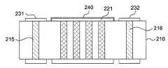
図2および図3に示すように、本発明の実施形態に係る発光素子パッケージの製造方法は、回路基板210を設ける過程を含む。まず、図2に示すように、回路基板210を1つの素子実装領域Aと、素子実装領域Aを基準にして左、右に位置した第1および第2電極配置領域B、Cに区分する。 As shown in FIGS. 2 and 3, the method for manufacturing a light emitting device package according to the embodiment of the present invention includes a process of providing a
回路基板210は、メタルコア印刷回路基板または絶縁物質を含む基板などであってもよい。ここで、絶縁物質を含む基板とは、印刷回路基板、セラミック基板、またはその他の様々な半導体基板上にFR1、FR2、FR3およびFR4のうちいずれか1つの絶縁物質がコーティングされたコアタイプの基板であってもよい。 The
素子実装領域A上に4個の第1ビアホールH1、H2、H3、H4を形成し、第1および第2電極配置領域B、C上にそれぞれ1つの第2ビアホールH5、H6を形成する。第1ビアホールH1、H2、H3、H4および第2ビアホールH5、H6はドリル加工によって形成してもよい。 Four first via holes H1, H2, H3, H4 are formed on the element mounting region A, and one second via hole H5, H6 is formed on each of the first and second electrode arrangement regions B, C. The first via holes H1, H2, H3, H4 and the second via holes H5, H6 may be formed by drilling.
その後、図3に示すように、第1ビアホールH1、H2、H3、H4内に金属物質を充填して4個の第1放熱ビア211、212、213、214を形成する。そして、第2ビアホールH5、H6内に金属物質を充填して2つの第2放熱ビア215、216を形成する。このとき、第1放熱ビア211、212、213、214、および第2放熱ビア215、216は、アルミニウム(Al)、銅(Cu)、モリブデン(Mo)、タングステン(W)、銀(Ag)、および半田のうち少なくとも1つ以上の金属物質を含んでもよい。 Thereafter, as shown in FIG. 3, the first via holes H1, H2, H3, and H4 are filled with a metal material to form four first
第1放熱ビア211、212、213、214は、素子実装領域Aの上部面および下部面上に露出した構造に形成されてもよく、第2放熱ビア215、216は、第1および第2電極配置領域B、Cの上部面および下部面上に露出した構造に形成されてもよい。 The first
図4に示すように、本発明の実施形態に係る発光素子パッケージの製造方法は、回路基板210上に第1放熱パッド221、第2放熱パッド222、第1電極パッド231、232、および第2電極パッド233、234を形成する過程を含んでもよい。 As shown in FIG. 4, the method for manufacturing a light emitting device package according to an embodiment of the present invention includes a first
具体的に、素子実装領域Aの上部面上に露出した第1放熱ビア211、212、213、214と接続されるように第1放熱パッド221を形成する。そして、第1および第2電極配置領域B、Cの上部面上に露出した第2放熱ビア215、216と接続されるように第1電極パッド231、232を形成する。 Specifically, the first
第1放熱パッド221および第1電極パッド231、232は1つの工程により製造してもよい。一例として、回路基板210の上部面の全体に金属物質を蒸着させた状態で、素子実装領域Aと第1および第2電極配置領域B、Cの間に蒸着された金属物質を選択的に除去する方式によって第1放熱パッド221および第1電極パッド231、232を形成してもよい。 The first
また、素子実装領域Aの下部面上に露出した第1放熱ビア211、212、213、214と接続されるように第2放熱パッド222を形成する。そして、第1および第2電極配置領域B、Cの下部面上に露出した第2放熱ビア215、216と接続されるように第2電極パッド233、234を形成する。 Further, the second
第2放熱パッド222および第2電極パッド233、234も1つの工程により製造してもよい。一例として、回路基板210の下部面の全体に金属物質を蒸着させた状態で、素子実装領域Aと第1および第2電極配置領域B、Cの間に蒸着された金属物質を選択的に除去する方式によって第2放熱パッド222および第2電極パッド233、234を形成してもよい。 The second
第1放熱パッド221、第2放熱パッド222、第1電極パッド231、232、および第2電極パッド233、234は、アルミニウム(Al)、銅(Cu)、モリブデン(Mo)、タングステン(W)、銀(Ag)、および半田のうち少なくとも1つ以上の金属物質に構成してもよい。この場合、各構成要素を構成している金属物質は全て同一であってもよく、互いに異なってもよい。 The first
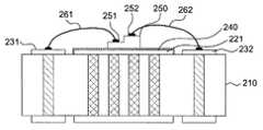
図5に示すように、本発明の実施形態に係る発光素子パッケージの製造方法は、第1放熱パッド221上に反射金属層240をコーティングする過程を含んでもよい。図4に示す回路基板210上で第1放熱パッド221の表面上に光に対する反射特性に優れる金(Au)、銀(Ag)、および白金(Pt)のうちいずれか1つの金属物質をコーティングして反射金属層240を形成してもよい。ここで、反射金属層240は、反射特性の他に放熱特性を有することで、0.1mm〜30mmの厚さに形成してもよい。好ましくは、反射金属層240は、10mm〜15mmの厚さに形成する。 As shown in FIG. 5, the method of manufacturing the light emitting device package according to the embodiment of the present invention may include a process of coating the
図6に示すように、本発明の実施形態に係る発光素子パッケージの製造方法は、反射金属層240の形成された第1放熱パッド221上に発光素子250を実装する過程を含んでもよい。発光素子250は、上部面に2つの電極251、252が位置する水平型の構造を有してもよく、窒化物系の半導体物質に構成してもよい。発光素子250を第1放熱パッド221上に実装した後、2つの電極251、252それぞれと2つの第1電極パッド231、232を第1および第2ワイヤー261、262に接続する。第1および第2ワイヤー261、262は金(Au)に構成してもよい。 As shown in FIG. 6, the method for manufacturing the light emitting device package according to the embodiment of the present invention may include a process of mounting the
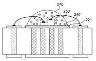
図7に示すように、本発明の実施形態に係る発光素子パッケージの製造方法は、発光素子250上部に蛍光体樹脂270を塗布する過程を含んでもよい。 As shown in FIG. 7, the method for manufacturing the light emitting device package according to the embodiment of the present invention may include a process of applying a
蛍光体樹脂270は、シリコン樹脂またはエポキシ樹脂、光の波長変換のための蛍光体および光拡散材が混合した物質であってもよい。蛍光体樹脂270は、発光素子250で発生する光の波長領域と、発光素子パッケージを用いて実現しようとする光の色によって少なくとも一種類以上の蛍光体を含んでもよい。例えば、蛍光体樹脂270は、YAG、TAG、LuAGなどの蛍光体を含んでもよい。また、蛍光体樹脂270は、蛍光体粒度の1/2以下、すなわち、ナノサイズの粒度を有する光拡散材を含んでもよい。光拡散材は白色の粒子であり、酸化アルミニウム(Al2O3)、二酸化珪素(SiO2)、および二酸化チタニウム(TiO2)のうちいずれか1つを含んでもよい。The
蛍光体樹脂270が塗布されると、蛍光体樹脂270に熱を加えて硬化させる工程を行なってもよい。 When the
図8に示すように、本発明の実施形態に係る発光素子パッケージの製造方法は、蛍光体樹脂270上にモールディング樹脂280を塗布する過程を含んでもよい。モールディング樹脂280は、発光素子250および蛍光体樹脂270を外部衝撃から保護するためのものであって、シリコン樹脂に構成してもよい。 As shown in FIG. 8, the method for manufacturing the light emitting device package according to the embodiment of the present invention may include a process of applying a
蛍光体樹脂270およびモールディング樹脂280は塗布の際に、樹脂物質の表面張力および粘度によってドーム状に形成してもよい。したがって、モールディング樹脂280と空気層との間の界面で光が屈折されて外部から抽出されるようにすることで、光抽出の効率を増加することができる。 The
図2〜図8に示す方法によって製造された発光素子パッケージ200は、「第1放熱パッド221(第1放熱ビア211、212、213、214)、第2放熱パッド222」に構成された第1列の伝達媒体と、「第1電極パッド231、232(第2放熱ビア215、216)、第2電極パッド233、234」に構成された第2列の伝達媒体を介して発光動作の際に発生する熱を効率よく放出することができる。したがって、発光素子パッケージ200の熱放出効率を向上させることができる。 The light emitting
上述したように本発明は限定された実施形態と図面によって説明したが、本発明は、上記の実施形態に限定されることなく、本発明が属する分野における通常の知識を有する者であれば、このような実施形態から多様な修正及び変形が可能である。 As described above, the present invention has been described with reference to the limited embodiments and drawings. However, the present invention is not limited to the above-described embodiments, and any person having ordinary knowledge in the field to which the present invention belongs can be used. Various modifications and variations are possible from such an embodiment.
したがって、本発明の範囲は、開示された実施形態に限定されて定められるものではなく、特許請求の範囲だけではなく特許請求の範囲と均等なものなどによって定められるものである。 Accordingly, the scope of the present invention is not limited to the disclosed embodiments, but is defined not only by the claims but also by the equivalents of the claims.
100、200 発光素子パッケージ
110、210 回路基板
111、112、113、114、211、212、213、214 第1放熱ビア
115、116、215、216 第2放熱ビア
121、221 第1放熱パッド
122、222 第2放熱パッド
131、132、231、232 第1電極パッド
133、134、233、234 第2電極パッド
140、240 反射金属層100, 200 Light emitting
Claims (16)
Translated fromJapanese前記素子実装領域の一方の面に接合して前記第1放熱ビアと接続される少なくとも1つの第1放熱パッドと、
前記第1放熱パッド上に実装された少なくとも1つの発光素子と、
前記電極配置領域の一方の面に接合して、各々が前記複数の第2放熱ビアのうちの対応する第2放熱ビアと接続される複数の第1電極パッドと、
前記発光素子と前記複数の第1電極パッドのうち対応する第1電極パッドとを電気的に接続する複数のワイヤーと
を備えることを特徴とする発光素子パッケージ。At least one element mounting region and a plurality of electrode placement regions, at least one first heat radiation via exposed on both surfaces of the device mounting region, and a plurality of second exposed on both surfaces of the plurality of electrode placement regions. A circuit board including heat dissipation vias;
At least one first heat dissipating pad joined to one surface of the element mounting region and connected to the first heat dissipating via;
At least one light emitting device mounted on the first heat dissipation pad;
A plurality of first electrode pads bonded to one surface of the electrode arrangement region and each connected to a corresponding second heat dissipation via of the plurality of second heat dissipation vias;
A light emitting device package comprising: a plurality of wires that electrically connect the light emitting device and a corresponding first electrode pad among the plurality of first electrode pads.
前記電極配置領域の他方の面に接合して、各々が前記複数の第2放熱ビアのうち対応する第2放熱ビアと接続される複数の第2電極パッドと
をさらに備えることを特徴とする請求項1に記載の発光素子パッケージ。At least one second heat dissipating pad joined to the other surface of the element mounting region and connected to the first heat dissipating via;
A plurality of second electrode pads, each of which is joined to the other surface of the electrode arrangement region and connected to a corresponding second heat dissipation via among the plurality of second heat dissipation vias. Item 2. A light emitting device package according to Item 1.
前記蛍光体層上に形成されたモールディング部と
をさらに備えることを特徴とする請求項7に記載の発光素子パッケージ。A phosphor layer formed on the light emitting element and containing a yellow phosphor;
The light emitting device package according to claim 7, further comprising: a molding part formed on the phosphor layer.
前記第1放熱ビアと接続されるように前記素子実装領域の一方の面に少なくとも1つの第1放熱パッドを形成するステップと、
前記電極配置領域の一方の面に、各々が前記複数の第2放熱ビアのうち対応する第2放熱ビアと接続されるように複数の第1電極パッドを形成するステップと、
前記第1放熱パッド上に少なくとも1つの発光素子を実装するステップと、
前記発光素子と前記第1電極パッドとが電気的に接続されるようにワイヤーボンディングするステップと
を含むことを特徴とする発光素子パッケージの製造方法。At least one element mounting region and a plurality of electrode placement regions, at least one first heat radiation via exposed on both surfaces of the device mounting region, and a plurality of second exposed on both surfaces of the plurality of electrode placement regions. Providing a circuit board including heat dissipation vias;
Forming at least one first heat dissipating pad on one surface of the element mounting region to be connected to the first heat dissipating via;
Forming a plurality of first electrode pads on one surface of the electrode arrangement region so as to be connected to a corresponding second heat dissipation via among the plurality of second heat dissipation vias;
Mounting at least one light emitting device on the first heat dissipation pad;
And a step of wire bonding so that the light emitting device and the first electrode pad are electrically connected to each other.
前記回路基板の素子実装領域上に少なくとも1つの第1ビアホールを形成するステップと、
前記回路基板の電極配置領域上に複数の第2ビアホールを形成するステップと、
前記第1ビアホール内に金属物質を充填して前記第1放熱ビアを形成するステップと、
前記第2ビアホール内に金属物質を充填して前記第2放熱ビアを形成するステップと
を含むことを特徴とする請求項10に記載の発光素子パッケージの製造方法。Providing the circuit board comprises:
Forming at least one first via hole on an element mounting region of the circuit board;
Forming a plurality of second via holes on the electrode placement region of the circuit board;
Filling the first via hole with a metal material to form the first heat dissipation via;
The method for manufacturing a light emitting device package according to claim 10, further comprising: filling the second via hole with a metal material to form the second heat dissipation via.
前記電極配置領域の他方の面に、各々が前記複数の第2放熱ビアのうち対応する第2放熱ビアと接続されるように複数の第2電極パッドを形成するステップと
をさらに含むことを特徴とする請求項10または11に記載の発光素子パッケージの製造方法。Forming at least one second heat dissipating pad on the other surface of the element mounting region to be connected to the first heat dissipating via;
Forming a plurality of second electrode pads on the other surface of the electrode arrangement region so as to be connected to a corresponding second heat dissipation via among the plurality of second heat dissipation vias. The method for manufacturing a light emitting device package according to claim 10 or 11.
前記蛍光体樹脂上にモールディング樹脂を塗布するステップと
をさらに含むことを特徴とする請求項15に記載の発光素子パッケージの製造方法。Applying a phosphor resin containing a yellow phosphor on the light emitting element;
The method of manufacturing a light emitting device package according to claim 15, further comprising: applying a molding resin on the phosphor resin.
Applications Claiming Priority (2)
| Application Number | Priority Date | Filing Date | Title |
|---|---|---|---|
| KR1020110022367AKR101847938B1 (en) | 2011-03-14 | 2011-03-14 | Light emitting device package and manufacturing method thereof |
| KR10-2011-0022367 | 2011-03-14 |
Publications (1)
| Publication Number | Publication Date |
|---|---|
| JP2012195587Atrue JP2012195587A (en) | 2012-10-11 |
Family
ID=45808305
Family Applications (1)
| Application Number | Title | Priority Date | Filing Date |
|---|---|---|---|
| JP2012057588APendingJP2012195587A (en) | 2011-03-14 | 2012-03-14 | Light-emitting element package and manufacturing method for the same |
Country Status (4)
| Country | Link |
|---|---|
| US (1) | US8866376B2 (en) |
| EP (1) | EP2500956A2 (en) |
| JP (1) | JP2012195587A (en) |
| KR (1) | KR101847938B1 (en) |
Cited By (1)
| Publication number | Priority date | Publication date | Assignee | Title |
|---|---|---|---|---|
| WO2017111320A1 (en)* | 2015-12-23 | 2017-06-29 | 엘지이노텍(주) | Light-emitting element package |
Families Citing this family (22)
| Publication number | Priority date | Publication date | Assignee | Title |
|---|---|---|---|---|
| KR20140021910A (en)* | 2012-08-13 | 2014-02-21 | 삼성전기주식회사 | Core substrate and printed circuit board using the same |
| KR200473652Y1 (en)* | 2012-10-25 | 2014-07-17 | 차오-친 예 | Led cooling structure |
| KR101415929B1 (en)* | 2012-11-28 | 2014-07-04 | 주식회사 루멘스 | Lighting device and lighting device assembly comprising the same |
| US9538633B2 (en)* | 2012-12-13 | 2017-01-03 | Nvidia Corporation | Passive cooling system integrated into a printed circuit board for cooling electronic components |
| WO2014092296A1 (en)* | 2012-12-14 | 2014-06-19 | ㈜ 아모엘이디 | Varistor substrate in which thermal via is formed, and method for manufacturing same |
| DE102013100470A1 (en)* | 2013-01-17 | 2014-07-17 | Osram Opto Semiconductors Gmbh | Optoelectronic semiconductor chip |
| CN103237412B (en)* | 2013-03-27 | 2016-03-23 | 苏州远创达科技有限公司 | A kind of soft copy mounting structure and manufacture method, soft copy product |
| JP5725076B2 (en)* | 2013-04-23 | 2015-05-27 | ウシオ電機株式会社 | Light emitting device for alternating current |
| US9502628B2 (en)* | 2013-11-06 | 2016-11-22 | Starlite Led Inc. | LED package and method of manufacturing the same |
| KR102295106B1 (en)* | 2014-12-04 | 2021-08-31 | 삼성전기주식회사 | Printed circuit board |
| US10429509B2 (en)* | 2014-12-24 | 2019-10-01 | Stmicroelectronics Pte Ltd. | Molded proximity sensor |
| KR102374209B1 (en)* | 2014-12-24 | 2022-03-15 | 삼성전기주식회사 | Printed circuit board |
| EP3268995B1 (en) | 2015-03-11 | 2019-09-18 | Koninklijke Philips N.V. | Light emitting device cooling |
| DE202015103290U1 (en)* | 2015-04-29 | 2016-08-01 | Tridonic Jennersdorf Gmbh | LED lens with integrated connection technology |
| JP6471641B2 (en)* | 2015-08-04 | 2019-02-20 | 日亜化学工業株式会社 | Method for manufacturing light emitting device |
| KR102634692B1 (en)* | 2016-02-12 | 2024-02-08 | 삼성전자주식회사 | Semiconductor light emitting device package |
| WO2018139790A1 (en)* | 2017-01-24 | 2018-08-02 | 엘지전자 주식회사 | Mobile/portable terminal |
| US10824054B2 (en) | 2017-01-24 | 2020-11-03 | Lg Electronics Inc. | Mobile terminal |
| DE102017104386A1 (en) | 2017-03-02 | 2018-09-06 | HELLA GmbH & Co. KGaA | Method for producing an electrical assembly |
| CN108198933B (en)* | 2018-01-02 | 2020-01-31 | 扬州乾照光电有限公司 | A kind of LED chip, preparation method and LED chip |
| CN111370556B (en)* | 2020-04-08 | 2021-04-30 | 广东良友科技有限公司 | A kind of LED bracket light source packaging structure and process thereof |
| WO2023117279A1 (en)* | 2021-12-22 | 2023-06-29 | Ams-Osram International Gmbh | Optoelectronic semiconductor device and method for producing an optoelectronic semiconductor device |
Citations (12)
| Publication number | Priority date | Publication date | Assignee | Title |
|---|---|---|---|---|
| JPH0945965A (en)* | 1995-07-26 | 1997-02-14 | Nichia Chem Ind Ltd | Ceramic LED package and manufacturing method thereof |
| JP2004282004A (en)* | 2002-09-17 | 2004-10-07 | Daiwa Kogyo:Kk | Light emitting element mounting substrate and method of manufacturing the same |
| WO2005029597A1 (en)* | 2003-09-19 | 2005-03-31 | Matsushita Electric Industrial Co., Ltd. | Illuminating device |
| JP2005209763A (en)* | 2004-01-21 | 2005-08-04 | Nichia Chem Ind Ltd | LIGHT EMITTING DEVICE AND LIGHT EMITTING DEVICE MANUFACTURING METHOD |
| JP2006041230A (en)* | 2004-07-28 | 2006-02-09 | Kyocera Corp | WIRING BOARD FOR LIGHT EMITTING ELEMENT AND LIGHT EMITTING DEVICE |
| JP2006294821A (en)* | 2005-04-08 | 2006-10-26 | Nichia Chem Ind Ltd | Light emitting device with excellent heat resistance and light resistance |
| JP2007173369A (en)* | 2005-12-20 | 2007-07-05 | Rohm Co Ltd | Semiconductor light-emitting element and manufacturing method thereof |
| JP2007273592A (en)* | 2006-03-30 | 2007-10-18 | Kyocera Corp | Light-emitting element wiring board and light-emitting device |
| JP2008227485A (en)* | 2007-03-14 | 2008-09-25 | Samsung Electro-Mechanics Co Ltd | LED package |
| JP2009010360A (en)* | 2007-05-31 | 2009-01-15 | Toshiba Lighting & Technology Corp | Lighting device |
| JP2009164311A (en)* | 2007-12-28 | 2009-07-23 | Sumitomo Metal Electronics Devices Inc | Substrate for mounting light emitting element and manufacturing method thereof, and light emitting device using same |
| JP2009239036A (en)* | 2008-03-27 | 2009-10-15 | Hitachi Aic Inc | Led substrate |
Family Cites Families (13)
| Publication number | Priority date | Publication date | Assignee | Title |
|---|---|---|---|---|
| JP2001297603A (en) | 2000-04-12 | 2001-10-26 | Bridgestone Corp | Linear luminous unit |
| DE10020465A1 (en)* | 2000-04-26 | 2001-11-08 | Osram Opto Semiconductors Gmbh | Radiation-emitting semiconductor component with luminescence conversion element |
| TW462121B (en)* | 2000-09-19 | 2001-11-01 | Siliconware Precision Industries Co Ltd | Heat sink type ball grid array package |
| US7196459B2 (en)* | 2003-12-05 | 2007-03-27 | International Resistive Co. Of Texas, L.P. | Light emitting assembly with heat dissipating support |
| TWI419375B (en)* | 2005-02-18 | 2013-12-11 | Nichia Corp | Light-emitting device with lens for controlling light distribution characteristics |
| US7808013B2 (en) | 2006-10-31 | 2010-10-05 | Cree, Inc. | Integrated heat spreaders for light emitting devices (LEDs) and related assemblies |
| TW200843130A (en) | 2007-04-17 | 2008-11-01 | Wen Lin | Package structure of a surface-mount high-power light emitting diode chip and method of making the same |
| KR20100037163A (en)* | 2007-07-30 | 2010-04-08 | 샤프 가부시키가이샤 | Clean room with light emitting device, lighting device and lighting device |
| JP5041593B2 (en) | 2007-08-28 | 2012-10-03 | シチズン電子株式会社 | Manufacturing method of chip type semiconductor device |
| JP2009117536A (en) | 2007-11-05 | 2009-05-28 | Towa Corp | Resin-sealed light emitting body and manufacturing method thereof |
| US20090273002A1 (en)* | 2008-05-05 | 2009-11-05 | Wen-Chih Chiou | LED Package Structure and Fabrication Method |
| KR101476422B1 (en) | 2008-06-30 | 2014-12-26 | 서울반도체 주식회사 | Printed circuit board and LED module using the same |
| US8337214B2 (en)* | 2009-11-13 | 2012-12-25 | Cree, Inc. | Electrical connectors and light emitting device package and methods of assembling the same |
- 2011
- 2011-03-14KRKR1020110022367Apatent/KR101847938B1/ennot_activeExpired - Fee Related
- 2012
- 2012-03-07USUS13/414,179patent/US8866376B2/ennot_activeExpired - Fee Related
- 2012-03-09EPEP12158692Apatent/EP2500956A2/ennot_activeWithdrawn
- 2012-03-14JPJP2012057588Apatent/JP2012195587A/enactivePending
Patent Citations (12)
| Publication number | Priority date | Publication date | Assignee | Title |
|---|---|---|---|---|
| JPH0945965A (en)* | 1995-07-26 | 1997-02-14 | Nichia Chem Ind Ltd | Ceramic LED package and manufacturing method thereof |
| JP2004282004A (en)* | 2002-09-17 | 2004-10-07 | Daiwa Kogyo:Kk | Light emitting element mounting substrate and method of manufacturing the same |
| WO2005029597A1 (en)* | 2003-09-19 | 2005-03-31 | Matsushita Electric Industrial Co., Ltd. | Illuminating device |
| JP2005209763A (en)* | 2004-01-21 | 2005-08-04 | Nichia Chem Ind Ltd | LIGHT EMITTING DEVICE AND LIGHT EMITTING DEVICE MANUFACTURING METHOD |
| JP2006041230A (en)* | 2004-07-28 | 2006-02-09 | Kyocera Corp | WIRING BOARD FOR LIGHT EMITTING ELEMENT AND LIGHT EMITTING DEVICE |
| JP2006294821A (en)* | 2005-04-08 | 2006-10-26 | Nichia Chem Ind Ltd | Light emitting device with excellent heat resistance and light resistance |
| JP2007173369A (en)* | 2005-12-20 | 2007-07-05 | Rohm Co Ltd | Semiconductor light-emitting element and manufacturing method thereof |
| JP2007273592A (en)* | 2006-03-30 | 2007-10-18 | Kyocera Corp | Light-emitting element wiring board and light-emitting device |
| JP2008227485A (en)* | 2007-03-14 | 2008-09-25 | Samsung Electro-Mechanics Co Ltd | LED package |
| JP2009010360A (en)* | 2007-05-31 | 2009-01-15 | Toshiba Lighting & Technology Corp | Lighting device |
| JP2009164311A (en)* | 2007-12-28 | 2009-07-23 | Sumitomo Metal Electronics Devices Inc | Substrate for mounting light emitting element and manufacturing method thereof, and light emitting device using same |
| JP2009239036A (en)* | 2008-03-27 | 2009-10-15 | Hitachi Aic Inc | Led substrate |
Cited By (2)
| Publication number | Priority date | Publication date | Assignee | Title |
|---|---|---|---|---|
| WO2017111320A1 (en)* | 2015-12-23 | 2017-06-29 | 엘지이노텍(주) | Light-emitting element package |
| US10559733B2 (en) | 2015-12-23 | 2020-02-11 | Lg Innotek Co., Ltd. | Light-emitting device package |
Also Published As
| Publication number | Publication date |
|---|---|
| EP2500956A2 (en) | 2012-09-19 |
| US20120236568A1 (en) | 2012-09-20 |
| KR101847938B1 (en) | 2018-04-13 |
| KR20120104761A (en) | 2012-09-24 |
| US8866376B2 (en) | 2014-10-21 |
Similar Documents
| Publication | Publication Date | Title |
|---|---|---|
| KR101847938B1 (en) | Light emitting device package and manufacturing method thereof | |
| CN104716247B (en) | Light emitting device | |
| JP6107510B2 (en) | Light emitting device and manufacturing method thereof | |
| US7755099B2 (en) | Light emitting device package | |
| US9420642B2 (en) | Light emitting apparatus and lighting apparatus | |
| US20150221830A1 (en) | Light emitting device package | |
| JP2008060542A (en) | LIGHT EMITTING DEVICE, LIGHT EMITTING DEVICE MANUFACTURING METHOD, AND LIGHT SOURCE DEVICE HAVING THE SAME | |
| US9966509B2 (en) | Light emitting apparatus and lighting apparatus | |
| WO2013168802A1 (en) | Led module | |
| JP6029188B2 (en) | LED package and manufacturing method thereof | |
| JP2012142430A (en) | Light-emitting device manufacturing method and light-emitting device | |
| JP6332251B2 (en) | Package manufacturing method, light emitting device manufacturing method, package, and light emitting device | |
| KR101012936B1 (en) | Light emitting diode package encapsulated using a light transmissive substrate and method of manufacturing the same | |
| CN104037305B (en) | Low-thermal-resistance wafer-level LED packaging method and packaging structure thereof | |
| KR20130051206A (en) | Light emitting module | |
| KR101363980B1 (en) | Optical module and manufacturing method thereof | |
| JP2007324204A (en) | Light emitting device | |
| JP6476703B2 (en) | Ceramic package, light emitting device, and manufacturing method thereof | |
| CN105826447A (en) | Package structure and method for fabricating the same | |
| TWI573299B (en) | Compound semiconductor device package module structure and fabricating method thereof | |
| KR20120104762A (en) | Light emitting device module and manufacturing method thereof | |
| CN106716652A (en) | Optoelectronic component | |
| TWI565101B (en) | Light emitting diode package and method for forming the same | |
| CN104465969A (en) | LED device and manufacturing method of LED device | |
| CN101814570A (en) | Light emitting device package and method for fabricating the same |
Legal Events
| Date | Code | Title | Description |
|---|---|---|---|
| A711 | Notification of change in applicant | Free format text:JAPANESE INTERMEDIATE CODE: A712 Effective date:20120814 | |
| RD04 | Notification of resignation of power of attorney | Free format text:JAPANESE INTERMEDIATE CODE: A7424 Effective date:20130321 | |
| A131 | Notification of reasons for refusal | Free format text:JAPANESE INTERMEDIATE CODE: A131 Effective date:20130625 | |
| A977 | Report on retrieval | Free format text:JAPANESE INTERMEDIATE CODE: A971007 Effective date:20130626 | |
| A521 | Request for written amendment filed | Free format text:JAPANESE INTERMEDIATE CODE: A523 Effective date:20130925 | |
| A02 | Decision of refusal | Free format text:JAPANESE INTERMEDIATE CODE: A02 Effective date:20131015 | |
| A521 | Request for written amendment filed | Free format text:JAPANESE INTERMEDIATE CODE: A523 Effective date:20140217 | |
| A911 | Transfer to examiner for re-examination before appeal (zenchi) | Free format text:JAPANESE INTERMEDIATE CODE: A911 Effective date:20140226 | |
| A912 | Re-examination (zenchi) completed and case transferred to appeal board | Free format text:JAPANESE INTERMEDIATE CODE: A912 Effective date:20140502 |