JP2012182312A - Method of manufacturing semiconductor device - Google Patents
Method of manufacturing semiconductor deviceDownload PDFInfo
- Publication number
- JP2012182312A JP2012182312AJP2011044217AJP2011044217AJP2012182312AJP 2012182312 AJP2012182312 AJP 2012182312AJP 2011044217 AJP2011044217 AJP 2011044217AJP 2011044217 AJP2011044217 AJP 2011044217AJP 2012182312 AJP2012182312 AJP 2012182312A
- Authority
- JP
- Japan
- Prior art keywords
- film
- semiconductor device
- silicon oxide
- manufacturing
- substrate
- Prior art date
- Legal status (The legal status is an assumption and is not a legal conclusion. Google has not performed a legal analysis and makes no representation as to the accuracy of the status listed.)
- Withdrawn
Links
Images


Classifications
- H—ELECTRICITY
- H10—SEMICONDUCTOR DEVICES; ELECTRIC SOLID-STATE DEVICES NOT OTHERWISE PROVIDED FOR
- H10B—ELECTRONIC MEMORY DEVICES
- H10B61/00—Magnetic memory devices, e.g. magnetoresistive RAM [MRAM] devices
- H—ELECTRICITY
- H01—ELECTRIC ELEMENTS
- H01L—SEMICONDUCTOR DEVICES NOT COVERED BY CLASS H10
- H01L21/00—Processes or apparatus adapted for the manufacture or treatment of semiconductor or solid state devices or of parts thereof
- H01L21/02—Manufacture or treatment of semiconductor devices or of parts thereof
- H01L21/02104—Forming layers
- H01L21/02107—Forming insulating materials on a substrate
- H01L21/02109—Forming insulating materials on a substrate characterised by the type of layer, e.g. type of material, porous/non-porous, pre-cursors, mixtures or laminates
- H01L21/02112—Forming insulating materials on a substrate characterised by the type of layer, e.g. type of material, porous/non-porous, pre-cursors, mixtures or laminates characterised by the material of the layer
- H01L21/02123—Forming insulating materials on a substrate characterised by the type of layer, e.g. type of material, porous/non-porous, pre-cursors, mixtures or laminates characterised by the material of the layer the material containing silicon
- H01L21/02164—Forming insulating materials on a substrate characterised by the type of layer, e.g. type of material, porous/non-porous, pre-cursors, mixtures or laminates characterised by the material of the layer the material containing silicon the material being a silicon oxide, e.g. SiO2
- H—ELECTRICITY
- H01—ELECTRIC ELEMENTS
- H01L—SEMICONDUCTOR DEVICES NOT COVERED BY CLASS H10
- H01L21/00—Processes or apparatus adapted for the manufacture or treatment of semiconductor or solid state devices or of parts thereof
- H01L21/02—Manufacture or treatment of semiconductor devices or of parts thereof
- H01L21/02104—Forming layers
- H01L21/02107—Forming insulating materials on a substrate
- H01L21/02109—Forming insulating materials on a substrate characterised by the type of layer, e.g. type of material, porous/non-porous, pre-cursors, mixtures or laminates
- H01L21/02205—Forming insulating materials on a substrate characterised by the type of layer, e.g. type of material, porous/non-porous, pre-cursors, mixtures or laminates the layer being characterised by the precursor material for deposition
- H01L21/02208—Forming insulating materials on a substrate characterised by the type of layer, e.g. type of material, porous/non-porous, pre-cursors, mixtures or laminates the layer being characterised by the precursor material for deposition the precursor containing a compound comprising Si
- H01L21/02219—Forming insulating materials on a substrate characterised by the type of layer, e.g. type of material, porous/non-porous, pre-cursors, mixtures or laminates the layer being characterised by the precursor material for deposition the precursor containing a compound comprising Si the compound comprising silicon and nitrogen
- H01L21/02222—Forming insulating materials on a substrate characterised by the type of layer, e.g. type of material, porous/non-porous, pre-cursors, mixtures or laminates the layer being characterised by the precursor material for deposition the precursor containing a compound comprising Si the compound comprising silicon and nitrogen the compound being a silazane
- H—ELECTRICITY
- H01—ELECTRIC ELEMENTS
- H01L—SEMICONDUCTOR DEVICES NOT COVERED BY CLASS H10
- H01L21/00—Processes or apparatus adapted for the manufacture or treatment of semiconductor or solid state devices or of parts thereof
- H01L21/02—Manufacture or treatment of semiconductor devices or of parts thereof
- H01L21/02104—Forming layers
- H01L21/02107—Forming insulating materials on a substrate
- H01L21/02296—Forming insulating materials on a substrate characterised by the treatment performed before or after the formation of the layer
- H01L21/02318—Forming insulating materials on a substrate characterised by the treatment performed before or after the formation of the layer post-treatment
- H01L21/02321—Forming insulating materials on a substrate characterised by the treatment performed before or after the formation of the layer post-treatment introduction of substances into an already existing insulating layer
- H01L21/02323—Forming insulating materials on a substrate characterised by the treatment performed before or after the formation of the layer post-treatment introduction of substances into an already existing insulating layer introduction of oxygen
- H01L21/02326—Forming insulating materials on a substrate characterised by the treatment performed before or after the formation of the layer post-treatment introduction of substances into an already existing insulating layer introduction of oxygen into a nitride layer, e.g. changing SiN to SiON
- H—ELECTRICITY
- H01—ELECTRIC ELEMENTS
- H01L—SEMICONDUCTOR DEVICES NOT COVERED BY CLASS H10
- H01L21/00—Processes or apparatus adapted for the manufacture or treatment of semiconductor or solid state devices or of parts thereof
- H01L21/02—Manufacture or treatment of semiconductor devices or of parts thereof
- H01L21/02104—Forming layers
- H01L21/02107—Forming insulating materials on a substrate
- H01L21/02296—Forming insulating materials on a substrate characterised by the treatment performed before or after the formation of the layer
- H01L21/02318—Forming insulating materials on a substrate characterised by the treatment performed before or after the formation of the layer post-treatment
- H01L21/02337—Forming insulating materials on a substrate characterised by the treatment performed before or after the formation of the layer post-treatment treatment by exposure to a gas or vapour
- H—ELECTRICITY
- H01—ELECTRIC ELEMENTS
- H01L—SEMICONDUCTOR DEVICES NOT COVERED BY CLASS H10
- H01L21/00—Processes or apparatus adapted for the manufacture or treatment of semiconductor or solid state devices or of parts thereof
- H01L21/02—Manufacture or treatment of semiconductor devices or of parts thereof
- H01L21/02104—Forming layers
- H01L21/02107—Forming insulating materials on a substrate
- H01L21/02296—Forming insulating materials on a substrate characterised by the treatment performed before or after the formation of the layer
- H01L21/02318—Forming insulating materials on a substrate characterised by the treatment performed before or after the formation of the layer post-treatment
- H01L21/02345—Forming insulating materials on a substrate characterised by the treatment performed before or after the formation of the layer post-treatment treatment by exposure to radiation, e.g. visible light
- H—ELECTRICITY
- H10—SEMICONDUCTOR DEVICES; ELECTRIC SOLID-STATE DEVICES NOT OTHERWISE PROVIDED FOR
- H10D—INORGANIC ELECTRIC SEMICONDUCTOR DEVICES
- H10D1/00—Resistors, capacitors or inductors
- H10D1/60—Capacitors
- H10D1/68—Capacitors having no potential barriers
Landscapes
- Engineering & Computer Science (AREA)
- Microelectronics & Electronic Packaging (AREA)
- Condensed Matter Physics & Semiconductors (AREA)
- General Physics & Mathematics (AREA)
- Manufacturing & Machinery (AREA)
- Computer Hardware Design (AREA)
- Physics & Mathematics (AREA)
- Power Engineering (AREA)
- Formation Of Insulating Films (AREA)
- Mram Or Spin Memory Techniques (AREA)
- Internal Circuitry In Semiconductor Integrated Circuit Devices (AREA)
- Semiconductor Memories (AREA)
- Hall/Mr Elements (AREA)
Abstract
Translated fromJapaneseDescription
Translated fromJapanese本発明の実施形態は、半導体装置の製造方法に関する。 Embodiments described herein relate generally to a method for manufacturing a semiconductor device.
次世代以降メモリとして、MRAM (Magnetoresistive Random Access Memory)が検討されている。MRAMは、トンネル磁気抵抗効果(Tunneling Magneto-Resistance Effect)を用いてデータの記憶を行うものである。 MRAM (Magnetoresistive Random Access Memory) has been studied as the next generation memory. The MRAM stores data using a tunneling magneto-resistance effect.
MRAMは、行列状に配置された複数のMTJ(Magnetic Tunnel Junction)素子を有する。各MTJ素子は、下部電極と上部電極との間に設けられた2つの磁性層と、この2つの磁性層に挟まれた1つの非磁性層とによる積層構造を有する。 The MRAM has a plurality of MTJ (Magnetic Tunnel Junction) elements arranged in a matrix. Each MTJ element has a laminated structure of two magnetic layers provided between the lower electrode and the upper electrode and one nonmagnetic layer sandwiched between the two magnetic layers.
MTJ素子の有する磁性層は耐熱性が低く、製造プロセスにおいて印加される熱により、MTJ素子の特性が変化してしまうことがある。そこで、MRAMを製造するためのプロセスにおいて、MTJ素子を形成した後は、MTJ素子を熱により劣化させないように、プロセス温度を所定の温度以下に例えば500℃以下に維持する必要がある。 The magnetic layer of the MTJ element has low heat resistance, and the characteristics of the MTJ element may change due to heat applied in the manufacturing process. Therefore, in the process for manufacturing the MRAM, after forming the MTJ element, it is necessary to maintain the process temperature at a predetermined temperature or lower, for example, 500 ° C. or lower so that the MTJ element is not deteriorated by heat.
また、各MTJ素子の間に、各MTJ素子を電気的に分離するための層間絶縁膜が設けられている。層間絶縁膜は、例えば酸化シリコン膜からなり、これを形成する方法として、ポリシラザン(PSZ)を用いる方法がある。 In addition, an interlayer insulating film for electrically isolating each MTJ element is provided between each MTJ element. The interlayer insulating film is made of, for example, a silicon oxide film, and there is a method using polysilazane (PSZ) as a method for forming the interlayer insulating film.
PSZを用いる方法は、詳細には、MTJ素子が設けられている基板の全面にPSZ溶液を塗布し、ベークしてPSZ溶液中の溶媒を揮発させ、次いで、酸素あるいは水蒸気を含む雰囲気で、波長の短い電磁波加熱、すなわち、紫外線、可視光、赤外線等を用いて600〜650℃にPSZを加熱する。 In detail, the method using PSZ applies the PSZ solution to the entire surface of the substrate on which the MTJ element is provided, baked to volatilize the solvent in the PSZ solution, and then in an atmosphere containing oxygen or water vapor, the wavelength PSZ is heated to 600 to 650 ° C. using short electromagnetic wave heating, that is, ultraviolet rays, visible light, infrared rays or the like.
本発明は、耐熱性に乏しいMTJ素子等の素子の劣化を避けつつ、良好な半導体装置を形成することができる半導体装置の製造方法を提供するものである。 The present invention provides a method for manufacturing a semiconductor device capable of forming a good semiconductor device while avoiding deterioration of an element such as an MTJ element having poor heat resistance.
本発明の実施形態によれば、半導体装置の製造方法は、基板上に複数の素子を形成し、前記複数の素子の間を埋め込むようにシリコン化合物膜を形成し、マイクロ波を照射することにより、前記シリコン化合物膜を酸化シリコン膜に改質することを備える。 According to an embodiment of the present invention, a method of manufacturing a semiconductor device includes forming a plurality of elements on a substrate, forming a silicon compound film so as to embed between the plurality of elements, and irradiating with a microwave. Modifying the silicon compound film into a silicon oxide film.
以下、図面を参照して、実施形態を説明する。ただし、本発明はこの実施形態に限定されるものではない。なお、全図面にわたり共通する部分には、共通する符号を付すものとし、重複する説明は省略する。また、図面は、実施形態の説明とその理解を促すための模式図であり、その形状や寸法、比などは実際の装置とは異なる個所もあるが、これらは以下の説明と公知の技術とを参酌して適宜、設計変更することができる。 Hereinafter, embodiments will be described with reference to the drawings. However, the present invention is not limited to this embodiment. In addition, the common code | symbol shall be attached | subjected to the part which is common throughout all drawings, and the overlapping description is abbreviate | omitted. The drawings are schematic diagrams for explaining the embodiment and promoting understanding thereof, and the shape, dimensions, ratios, and the like thereof are different from those of the actual apparatus. However, these are the following descriptions and known techniques. The design can be changed as appropriate in consideration of the above.
(第1の実施形態)
本実施形態の半導体装置の製造方法を図1から図4を用いて説明する。図1から図3は、本実施形態の半導体装置の製造工程における半導体装置の断面図を示すものである。図4は、本実施形態の製造装置を模式的に示す図である。以下、MRAM100の製造方法を例に説明するが、本発明は、このような半導体装置に限定されるものではなく、他の種類の半導体装置においても用いることができ、例えば、耐熱性に乏しい抵抗可変素子を有するReRAM(Resistance change Random Access Memory)といったクロスポイントメモリの製造方法においても用いることができる。(First embodiment)
A method for manufacturing the semiconductor device of this embodiment will be described with reference to FIGS. 1 to 3 are sectional views of the semiconductor device in the manufacturing process of the semiconductor device of this embodiment. FIG. 4 is a diagram schematically showing the manufacturing apparatus of the present embodiment. Hereinafter, the manufacturing method of the
まず、複数のMTJ素子10が行列状に形成された基板1を準備する。図1(a)に示されるように、MTJ素子10は、先に説明したように、例えば、下部電極(不図示)と上部電極(不図示)との間に設けられた2つの磁性層(不図示)と、この2つの磁性層に挟まれた1つの非磁性層(不図示)とによる積層構造を有する。さらに、各MTJ素子10の下部側壁は、下部層間絶縁膜3で覆われている。この下部層間絶縁膜3は、例えばPSZ(ポリシラザン)から形成された酸化シリコン膜である。この下部層間絶縁膜3は、MTJ素子10を形成する前に形成するため、高温になるような公知の方法を用いて形成しても良く、また、以下に説明する本実施形態を用いて形成しても良い。 First, a
次に、図1(b)に示すように、基板1の全面に、例えばPSZ溶液(シリコン化合物溶液)4を塗布する。このPSZの主成分は、シリコン、窒素、水素である。PSZ溶液4を塗布することにより、PSZ溶液4を段差被覆性良くMTJ素子10の間に、埋め込むことができる。 Next, as shown in FIG. 1B, for example, a PSZ solution (silicon compound solution) 4 is applied to the entire surface of the
次に、図2(a)に示すように、200℃から300℃の間の温度でベークして、PSZ溶液4に含まれている溶媒を揮発させ、PSZ膜(シリコン化合物膜)5をMTJ素子10の上とMTJ素子10の間とに形成する。なお、溶媒が分極を持つ分子構造を有する場合には、次の工程でマイクロ波を照射した際に溶媒が揮発するため、このベークを省略することもできる。 Next, as shown in FIG. 2A, the solvent contained in the
この後、図2(b)に示すように、酸素又は水蒸気を含む雰囲気下でマイクロ波を基板1に照射して、PSZ膜5を酸化シリコン膜6に改質する。詳細には、PSZ膜5に含まれる窒素が、雰囲気中の酸素と入れ替わり、水素が脱離することで、PSZ膜5が酸化シリコン膜6へと改質する。 Thereafter, as shown in FIG. 2B, the
マイクロ波の照射の際の酸素又は水蒸気を含む雰囲気の圧力は、マイクロ波を用いてもラジカルを発生させない程度の圧力であることが好ましく、例えば、大気圧又は大気圧よりも若干低い圧力である。ラジカルを発生させてしまうと、そのラジカルによりPSZ膜5の改質反応が過剰に促進され、酸化シリコン膜6中に、化学量論比よりも多く酸素を取り込んでしまうことがある。この多く取り込んだ酸素によって、酸化シリコン膜6中に電荷が生じ、その結果、酸化シリコン膜6の耐圧やリーク電流といった特性を悪化させることとなる。従って、これを避けることができるよう、ラジカルを発生させない程度の圧力が好ましい。 The pressure of the atmosphere containing oxygen or water vapor at the time of microwave irradiation is preferably a pressure that does not generate radicals even if microwaves are used, for example, atmospheric pressure or a pressure slightly lower than atmospheric pressure. . When radicals are generated, the reforming reaction of the
マイクロ波を照射する際の条件は、基板1の温度をできるだけ上げることがないような条件にすることが好ましく、例えば、基板1の基板温度が例えば200〜400℃の範囲となるような条件に設定する。このようにすることにより、基板1を低温に保ち、耐熱性に乏しいMTJ素子10の劣化を避けることができる。なお、この際の基板1の基板温度は、基板1の裏面にあるパイロメータを用いて確認する。 The conditions for irradiating the microwave are preferably such that the temperature of the
ただし、本実施形態においては、マイクロ波は、2.45GHzから25GHzの周波数を有する電磁波であることが好ましく、言い換えると、1.2cmから12.3cmの波長を有する電磁波であることが好ましい。また、本実施形態においては、マイクロ波の照射時間を30秒から30分にすることが好ましい。 However, in the present embodiment, the microwave is preferably an electromagnetic wave having a frequency of 2.45 GHz to 25 GHz, in other words, an electromagnetic wave having a wavelength of 1.2 cm to 12.3 cm. In the present embodiment, the microwave irradiation time is preferably 30 seconds to 30 minutes.
また、マイクロ波の照射パワーについては、以下のようにすることが好ましい。すなわち、図4に示されるように、マイクロ波を照射する際に用いられる製造装置20は、1つ又は複数の導波管21を有する(例えば、図4中では、製造装置20は4つの導波管21を有する)。この導波管21は、マグネトロン等のマイクロ波発振装置(不図示)から出力されたマイクロ波Wn(図4中では、W1からW4)を基板1が設置される製造装置20の内部に導くためのものである。そして、マイクロ波の照射パワー、詳細には、各導波管21から出力される各マイクロ波WnのパワーPWnを対応する各導波管21の断面積Snで割ったものの総和Σ(PWn/Sn)が、10W/cm2〜1kW/cm2となるように調整することが好ましい。例えば、図4で示される4つの導波管21を有する製造装置20を用いて説明すると、各導波管21の断面積をS1からS4とし、各導波管21から出力されるマイクロ波W1からW4のパワーをPW1からPW4とした場合、各導波管21から出力されるマイクロ波のパワーを各導波管21の断面積で割ったもの(PW1〜4/S1〜4)の総和、すなわち、PW1/S1+PW2/S2+PW3/S3+PW4/S4が、10W/cm2〜1kW/cm2となるように、マイクロ波の照射パワーを調整することが好ましい。よって、上記のように定義されたマイクロ波の照射パワーは、製造装置20の有する導波管21が増えるにしたがい、増えることとなる。The microwave irradiation power is preferably as follows. That is, as shown in FIG. 4, the
そして、図3に示すように、CMP(Chemical Mechanical Polishing)法を用いて、MTJ素子10の上面が露出するまで、酸化シリコン膜6を研磨する。このようにして、MTJ素子10の間に上部層間絶縁膜として酸化シリコン膜6を設け、MRAM100を形成する。 Then, as shown in FIG. 3, the
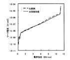
本実施形態により形成された酸化シリコン膜6の特性、詳細には、リーク電流密度及び破壊電界強度の測定を行った。 The characteristics of the
まず、シリコン基板上にPSZ膜を形成し、本実施形態と同様の方法を用いて、言い換えると、PSZ膜にマイクロ波を照射して酸化シリコン膜に改質し、さらに、その上に電極を形成した。このようにして得たキャパシタ構造に対して、水銀プローブ法により電圧を印加して電流を測定することによって、リーク電流密度及び破壊電界強度を測定した。 First, a PSZ film is formed on a silicon substrate, and using the same method as in this embodiment, in other words, the PSZ film is irradiated with microwaves to be modified into a silicon oxide film, and an electrode is further formed thereon. Formed. A leakage current density and a breakdown electric field strength were measured by applying a voltage to the capacitor structure thus obtained by a mercury probe method and measuring a current.
さらに、比較例として、シリコン基板上にPSZ膜を形成し、マイクロ波を照射するかわりに、600〜650℃の酸素又は水蒸気を含む雰囲気でPSZ膜を加熱して酸化シリコン膜に改質し、その上に電極を形成した。この比較例のキャパシタ構造に対しても、上記と同様に、リーク電流密度及び破壊電界強度の測定をした。 Furthermore, as a comparative example, instead of forming a PSZ film on a silicon substrate and irradiating with a microwave, the PSZ film is heated in an atmosphere containing oxygen or water vapor at 600 to 650 ° C. to be modified into a silicon oxide film, An electrode was formed thereon. For the capacitor structure of this comparative example, the leakage current density and the breakdown electric field strength were measured in the same manner as described above.
図5に結果を示す。図5の横軸は、印加電圧を各キャパシタ構造の酸化シリコン膜の厚さで割った値、すなわち電界強度(単位:V/cm)を示し、図5の縦軸は、リーク電流を各キャパシタの電極の面積で割った値、すなわちリーク電流密度(単位:A/cm2)を示す。この図からわかるように、リーク電流密度、破壊電界強度ともに、本実施形態によるキャパシタ構造は、比較例のキャパシタ構造のものとほぼ同じ結果を示した。すなわち、本実施形態による、言い換えると、マイクロ波を照射することによりPSZ膜を改質して得た酸化シリコン膜は、600〜650℃の酸素又は水蒸気を含む雰囲気でPSZ膜を加熱することによって得た酸化シリコン膜と同等の、リーク電流特性及び耐圧特性を有する。The results are shown in FIG. The horizontal axis of FIG. 5 shows the value obtained by dividing the applied voltage by the thickness of the silicon oxide film of each capacitor structure, that is, the electric field strength (unit: V / cm), and the vertical axis of FIG. The value divided by the electrode area, that is, the leakage current density (unit: A / cm2 ) is shown. As can be seen from this figure, both the leakage current density and the breakdown electric field strength showed almost the same result as that of the capacitor structure of the comparative example. That is, in other words, the silicon oxide film obtained by modifying the PSZ film by irradiating microwaves is heated by heating the PSZ film in an atmosphere containing oxygen or water vapor at 600 to 650 ° C. It has leakage current characteristics and breakdown voltage characteristics equivalent to the obtained silicon oxide film.
また、本実施形態により形成された酸化シリコン膜6の希フッ酸溶液に対するエッチングレートを測定した。 Further, the etching rate of the
まず、シリコン基板上にPSZ膜を形成し、本実施形態と同様の方法を用いて、言い換えると、PSZ膜にマイクロ波を照射して、酸化シリコン膜を形成した。この酸化シリコン膜の膜厚をエリプソメーターであらかじめ測定した。さらに、酸化シリコン膜を所定の時間、所定の温度、所定の濃度の希フッ酸溶液に浸漬し、再度、酸化シリコン膜の膜厚をエリプソメーターで測定した。この測定結果を用いて、エッチングレートを算出した。 First, a PSZ film was formed on a silicon substrate, and using the same method as in this embodiment, in other words, the PSZ film was irradiated with microwaves to form a silicon oxide film. The thickness of this silicon oxide film was measured in advance with an ellipsometer. Further, the silicon oxide film was immersed in a dilute hydrofluoric acid solution having a predetermined temperature and a predetermined concentration for a predetermined time, and the thickness of the silicon oxide film was again measured with an ellipsometer. Using this measurement result, an etching rate was calculated.
さらに、比較例として、シリコン基板上にPSZ膜を形成し、マイクロ波を照射するかわりに、600〜650℃の酸素又は水蒸気を含む雰囲気でPSZ膜を加熱して、酸化シリコン膜を形成した。この比較例についても、上記と同様に、エッチングレートを算出した。 Further, as a comparative example, instead of forming a PSZ film on a silicon substrate and irradiating with microwaves, the PSZ film was heated in an atmosphere containing oxygen or water vapor at 600 to 650 ° C. to form a silicon oxide film. For this comparative example, the etching rate was calculated in the same manner as described above.
このように算出されたエッチングレートについても、本実施形態による酸化シリコン膜は、比較例の酸化シリコン膜とほぼ同じ結果を示した。すなわち、本実施形態による、言い換えると、マイクロ波を照射することによりPSZ膜を改質して得た酸化シリコン膜は、600〜650℃の酸素又は水蒸気を含む雰囲気でPSZ膜を加熱することによって得た酸化シリコン膜と同等の、エッチングレートを有する。 Regarding the etching rate calculated in this way, the silicon oxide film according to the present embodiment showed almost the same result as the silicon oxide film of the comparative example. That is, in other words, the silicon oxide film obtained by modifying the PSZ film by irradiating microwaves is heated by heating the PSZ film in an atmosphere containing oxygen or water vapor at 600 to 650 ° C. It has an etching rate equivalent to that of the obtained silicon oxide film.
すなわち、本実施形態によれば、マイクロ波が5cm程度の長い波長を有することから、照射したマイクロ波がMTJ素子10の間にあるPSZ膜5の奥まで届き、効果的にPSZ膜5を酸化シリコン膜6へと改質することができる。さらに、従来のように、マイクロ波より波長の短い電磁波加熱、すなわち、紫外線、可視光、赤外線等を用いて加熱することによりPSZ膜5を改質するのではなく、マイクロ波の作用によりPSZ膜5を改質するため、基板温度が高くなることを避けることができる。従って、酸化シリコン膜6の形成の際に、耐熱性に乏しいMTJ素子10が劣化することを避けつつ、破壊耐圧が高く、リーク電流も抑えられるような酸化シリコン膜6を得ることができ、よって、良好なMRAM100の形成することができる。 That is, according to this embodiment, since the microwave has a long wavelength of about 5 cm, the irradiated microwave reaches the depth of the
例えば、紫外線を照射してPSZ膜5の改質を行った場合、紫外線の波長は100nm程度と短いため、照射した紫外線がMTJ素子10の間にあるPSZ膜5の奥まで届きにくい。従って、効果的にPSZ膜5を酸化シリコン膜6へと改質することが難しい。また、紫外線はそのエネルギーが高いため、紫外線照射によるPSZ膜5の改質反応が過剰に促進され、生成される酸化シリコン膜6中に、化学量論比よりも多く酸素を取り込んでしまうことがある。このような多く取り込んだ酸素によって、酸化シリコン膜6中に電荷が生じ、その結果、耐圧やリーク電流といった酸化シリコン膜6の特性を悪化させることとなる。 For example, when the
一方、本実施形態においては、マイクロ波を照射して、PSZ膜5中の分極した分子を回転させて、穏やかにPSZ膜5の改質反応を行う。従って、酸化シリコン膜6中に化学量論比よりも多く酸素を取り込み、電荷が生じることを避けることができ、よって、耐圧やリーク電流といった酸化シリコン膜6の特性を悪化させることを避けることができる。 On the other hand, in this embodiment, microwaves are irradiated to rotate the polarized molecules in the
さらに、本実施形態においては、マイクロ波を用いることにより、紫外線を用いた場合と比べて、半導体装置100を製造する際の消費電力が少ない。また、マイクロ波は石英を透過するため、製造装置に組み込むことが容易である。 Furthermore, in this embodiment, the use of microwaves reduces the power consumption when manufacturing the
(第2の実施形態)
上部層間絶縁膜としての酸化シリコン膜6を形成するために、第1の実施形態においては、シリコン化合物材料としてPSZ膜5を用いていたが、本実施形態では、有機SOG(Spin on Glass)を用いる。この有機SOGの主成分は、シリコン、酸素、炭素、水素である。有機SOGを用いることにより、MTJ素子10の間に酸化シリコン膜6を形成する際に基板1に生じる応力が、PSZ膜5に比べて小さいため、基板1に欠陥が生ずることをより避けることができる。さらに有機SOGを用いることにより、有機SOGにより形成した酸化シリコン膜6中には、PSZ膜を用いて形成した場合と比べて残留する窒素が少ないため、酸化シリコン膜6中に窒素による固定電荷が発生することを抑制することができる。(Second Embodiment)
In order to form the
第2の実施形態の半導体装置の製造方法を説明するための図は、第1の実施形態の説明で用いられた図と同様に示されるため、第2の実施形態にかかる半導体装置の製造方法を、図1から図3を用いて説明する。ここでは、第1の実施形態と共通する部分については、詳細な説明を省略する。なお、以下、MRAM100の製造方法を例に説明するが、第1の実施形態と同様に、本発明は、このような半導体装置に限定されるものではなく、他の種類の半導体装置においても用いることができ、例えば、耐熱性に乏しい抵抗可変素子を有するReRAMといったクロスポイントメモリの製造方法において用いることができる。 Since the drawing for explaining the manufacturing method of the semiconductor device of the second embodiment is shown in the same manner as the drawing used in the description of the first embodiment, the manufacturing method of the semiconductor device according to the second embodiment Will be described with reference to FIGS. 1 to 3. Here, detailed description of portions common to the first embodiment is omitted. In the following, a method for manufacturing the
まず、第1の実施形態と同様に、図1(a)に示されるように、複数のMTJ素子10が行列状に形成された基板1を準備する。 First, as in the first embodiment, as shown in FIG. 1A, a
次に、図1(b)に示すように、基板1の全面に、有機SOG溶液(シリコン化合物材料)4を塗布する。有機SOG溶液4を塗布することにより、有機SOG溶液4を段差被覆性良くMTJ素子10の間に、埋め込むことができる。 Next, as shown in FIG. 1B, an organic SOG solution (silicon compound material) 4 is applied to the entire surface of the
次に、図2(a)に示すように、200℃から300℃の温度でベークして、有機SOG溶液4に含まれている溶媒を揮発させ、有機SOG膜(シリコン化合物膜)5をMTJ素子の上とその間とに形成する。なお、溶媒が分極を持つ分子構造を有する場合には、第1の実施形態と同様に、次の工程でマイクロ波を照射した際に溶媒が揮発するため、このベークを省略することもできる。 Next, as shown in FIG. 2A, baking is performed at a temperature of 200 ° C. to 300 ° C. to volatilize the solvent contained in the
この後、図2(b)に示すように、窒素又はアルゴン等の不活性ガスを含む雰囲気下で、好ましくは酸素を含まない雰囲気下で、マイクロ波を基板1に照射して、有機SOG膜5を酸化シリコン膜6に改質する。詳細には、有機SOG膜5に含まれる有機官能基が脱離することにより、有機SOG膜5が酸化シリコン膜6へと改質する。 Thereafter, as shown in FIG. 2B, the
マイクロ波を照射する際の条件は、第1の実施形態と同様に、基板1の温度をできるだけ上げることがないような条件にすることが好ましく、例えば、基板1の基板温度が例えば200〜400℃の範囲となるような条件に設定する。このようにすることにより、基板1を低温に保ち、耐熱性に乏しいMTJ素子10の劣化を避けることができる。なお、詳細なマイクロ波の照射条件(圧力、周波数、照射時間、照射パワー)については、第1の実施形態と同様であるため、ここでは説明を省略する。 As in the first embodiment, it is preferable that the microwave irradiation is performed so that the temperature of the
そして、図3に示すように、CMP法を用いて、MTJ素子10の上面が露出するまで、酸化シリコン膜6を研磨する。このようにして、MTJ素子10の間に上部層間絶縁膜として酸化シリコン膜6を設け、MRAM100を形成する。 Then, as shown in FIG. 3, the
すなわち、本実施形態によれば、マイクロ波を照射することにより、マイクロ波がMTJ素子10の間にある有機SOG膜5の奥まで届くことから、効果的に有機SOG膜5を酸化シリコン膜6へと改質することができる。さらに、従来のように、加熱することにより有機SOG膜5を改質するのではなく、マイクロ波の作用により有機SOG膜5を改質するため、基板温度が高くなることを避けることができる。従って、酸化シリコン膜6の形成の際に、耐熱性に乏しいMTJ素子10が劣化することを避けつつ、破壊耐圧が高く、リーク電流も抑えられるような酸化シリコン膜6を得ることができ、よって、良好なMRAM100の形成することができる。 That is, according to the present embodiment, by irradiating microwaves, the microwaves reach the depth of the
また、本実施形態によれば、有機SOGを用いることにより、MTJ素子10の間に酸化シリコン膜6を形成する際に基板1に生じる応力を小さくして、基板1に欠陥が生ずることを避けることができる。さらに、酸化シリコン膜6中に残留する窒素を少なくして、酸化シリコン膜6中に固定電荷が発生することを抑制することができる。 Further, according to the present embodiment, by using organic SOG, the stress generated in the
そして、本実施形態においても、マイクロ波を用いることにより、紫外線を用いた場合と比べて半導体装置100を製造する際の消費電力が少ない。また、マイクロ波は石英を透過するため、製造装置に組み込むことが容易である。 Also in the present embodiment, the use of microwaves reduces the power consumption when manufacturing the
なお、上記の第1及び第2の実施形態においては、基板1は、必ずしもシリコン基板でなくてもよく、他の基板(例えば、SOI(Silicon on insulator)基板やSiGe基板など)でも良い。また、このような種々の基板上に半導体構造等が形成されたものでも良い。 In the first and second embodiments described above, the
本発明の実施形態を説明したが、これらの実施形態は、例として提示したものであり、発明の範囲を限定することは意図していない。これら新規な実施形態は、その他の様々な形態で実施されることが可能であり、発明の要旨を逸脱しない範囲で、種々の省略、置き換え、変更を行うことができる。これら実施形態やその変形は、発明の範囲や要旨に含まれるとともに、特許請求の範囲に記載された発明とその均等の範囲に含まれる。 Although the embodiments of the present invention have been described, these embodiments are presented as examples, and are not intended to limit the scope of the invention. These novel embodiments can be implemented in various other forms, and various omissions, replacements, and changes can be made without departing from the scope of the invention. These embodiments and modifications thereof are included in the scope and gist of the invention, and are included in the invention described in the claims and the equivalents thereof.
1 基板
3 下部層間絶縁膜
4 PSZ溶液、有機SOG溶液
5 PSZ膜、有機SOG膜(シリコン化合物膜)
6 酸化シリコン膜(上部層間絶縁膜)
10 MTJ素子
20 製造装置
21 導波管
100 MRAM(半導体装置)
S1、S2、S3、S4 断面積
W1、W2、W3、W4 マイクロ波1
6 Silicon oxide film (upper interlayer insulating film)
10
S1 , S2 , S3 , S4 cross-sectional areas W1 , W2 , W3 , W4 microwaves
Claims (6)
Translated fromJapanese前記複数の素子の間を埋め込むように、シリコン化合物膜を形成し、
マイクロ波を照射することにより、前記シリコン化合物膜を酸化シリコン膜に改質する、
ことを備える半導体装置の製造方法。A plurality of elements are formed on the substrate,
A silicon compound film is formed so as to embed between the plurality of elements,
By irradiating microwaves, the silicon compound film is modified into a silicon oxide film.
A method of manufacturing a semiconductor device.
Priority Applications (2)
| Application Number | Priority Date | Filing Date | Title |
|---|---|---|---|
| JP2011044217AJP2012182312A (en) | 2011-03-01 | 2011-03-01 | Method of manufacturing semiconductor device |
| US13/249,503US8552411B2 (en) | 2011-03-01 | 2011-09-30 | Manufacturing method of semiconductor device |
Applications Claiming Priority (1)
| Application Number | Priority Date | Filing Date | Title |
|---|---|---|---|
| JP2011044217AJP2012182312A (en) | 2011-03-01 | 2011-03-01 | Method of manufacturing semiconductor device |
Publications (1)
| Publication Number | Publication Date |
|---|---|
| JP2012182312Atrue JP2012182312A (en) | 2012-09-20 |
Family
ID=46753569
Family Applications (1)
| Application Number | Title | Priority Date | Filing Date |
|---|---|---|---|
| JP2011044217AWithdrawnJP2012182312A (en) | 2011-03-01 | 2011-03-01 | Method of manufacturing semiconductor device |
Country Status (2)
| Country | Link |
|---|---|
| US (1) | US8552411B2 (en) |
| JP (1) | JP2012182312A (en) |
Cited By (1)
| Publication number | Priority date | Publication date | Assignee | Title |
|---|---|---|---|---|
| JP2020047665A (en)* | 2018-09-14 | 2020-03-26 | 株式会社東芝 | Semiconductor device, manufacturing method thereof, inverter circuit, drive device, vehicle, and elevator |
Families Citing this family (4)
| Publication number | Priority date | Publication date | Assignee | Title |
|---|---|---|---|---|
| JP5981206B2 (en)* | 2012-04-20 | 2016-08-31 | 株式会社東芝 | Semiconductor device manufacturing method and semiconductor manufacturing apparatus |
| JP6596285B2 (en) | 2015-09-24 | 2019-10-23 | 東芝メモリ株式会社 | Microwave irradiation apparatus and substrate processing method |
| US10062843B2 (en) | 2015-12-11 | 2018-08-28 | Samsung Electronics Co., Ltd. | Variable resistive memory device and method of manufacturing the same |
| US10475987B1 (en) | 2018-05-01 | 2019-11-12 | Taiwan Semiconductor Manufacturing Company, Ltd. | Method for fabricating a magnetic tunneling junction (MTJ) structure |
Family Cites Families (13)
| Publication number | Priority date | Publication date | Assignee | Title |
|---|---|---|---|---|
| JPH0493029A (en) | 1990-08-08 | 1992-03-25 | Nec Corp | Manufacture of semiconductor device |
| JPH04338644A (en) | 1991-05-16 | 1992-11-25 | Casio Comput Co Ltd | Method for forming interlayer insulating film of semiconductor device |
| US6194038B1 (en)* | 1998-03-20 | 2001-02-27 | Applied Materials, Inc. | Method for deposition of a conformal layer on a substrate |
| US6685920B2 (en) | 1999-11-12 | 2004-02-03 | The Procter & Gamble Company | Method of protecting teeth against erosion |
| JP4731694B2 (en)* | 2000-07-21 | 2011-07-27 | 東京エレクトロン株式会社 | Semiconductor device manufacturing method and substrate processing apparatus |
| JP4142993B2 (en)* | 2003-07-23 | 2008-09-03 | 株式会社東芝 | Method for manufacturing magnetic memory device |
| JP5177617B2 (en) | 2006-12-25 | 2013-04-03 | 独立行政法人産業技術総合研究所 | Silicon oxide thin film forming equipment |
| US8080463B2 (en)* | 2009-01-23 | 2011-12-20 | Kabushiki Kaisha Toshiba | Semiconductor device manufacturing method and silicon oxide film forming method |
| JP2011035371A (en) | 2009-07-07 | 2011-02-17 | Toshiba Corp | Method and apparatus for manufacturing semiconductor device |
| JP5537102B2 (en) | 2009-09-11 | 2014-07-02 | 株式会社東芝 | Manufacturing method of semiconductor device |
| JP5297323B2 (en) | 2009-09-30 | 2013-09-25 | 株式会社東芝 | Manufacturing method of semiconductor device |
| JP5433462B2 (en) | 2010-03-03 | 2014-03-05 | 株式会社東芝 | Manufacturing method of semiconductor device |
| JP2011199035A (en)* | 2010-03-19 | 2011-10-06 | Toshiba Corp | Semiconductor memory device |
- 2011
- 2011-03-01JPJP2011044217Apatent/JP2012182312A/ennot_activeWithdrawn
- 2011-09-30USUS13/249,503patent/US8552411B2/ennot_activeExpired - Fee Related
Cited By (2)
| Publication number | Priority date | Publication date | Assignee | Title |
|---|---|---|---|---|
| JP2020047665A (en)* | 2018-09-14 | 2020-03-26 | 株式会社東芝 | Semiconductor device, manufacturing method thereof, inverter circuit, drive device, vehicle, and elevator |
| JP7005847B2 (en) | 2018-09-14 | 2022-01-24 | 株式会社東芝 | Semiconductor devices, manufacturing methods for semiconductor devices, inverter circuits, drives, vehicles, and elevators |
Also Published As
| Publication number | Publication date |
|---|---|
| US20120225498A1 (en) | 2012-09-06 |
| US8552411B2 (en) | 2013-10-08 |
Similar Documents
| Publication | Publication Date | Title |
|---|---|---|
| KR101558192B1 (en) | Method for manufacturing semiconductor substrate and method for manufacturing semiconductor device | |
| TWI455245B (en) | Method of manufacturing a semiconductor device | |
| TWI514520B (en) | Semiconductor substrate and method of manufacturing same | |
| TWI360832B (en) | Multi-step system and method for curing a dielectr | |
| KR101379409B1 (en) | Manufacturing process of a structure of semiconductor on insulator type, with reduced electrical losses and corresponding structure | |
| TWI527151B (en) | Method for producing an SOI substrate and a semiconductor device | |
| TWI493609B (en) | Semiconductor substrate, display panel, and method of manufacturing display device | |
| JP5387586B2 (en) | Silicon oxide film forming method, liner film forming method, and semiconductor device manufacturing method | |
| JP2012182312A (en) | Method of manufacturing semiconductor device | |
| US20140004690A1 (en) | Method of manufacturing semiconductor device | |
| CN104992901A (en) | Method for providing lateral thermal processing of thin films on low-temperature substrates | |
| CN112537796B (en) | Low-energy light-excited material nondestructive thinning method | |
| Lin et al. | Realizing High Brightness Quasi‐2D Perovskite Light‐Emitting Diodes with Reduced Efficiency Roll‐Off via Multifunctional Interface Engineering | |
| JP2013073950A (en) | Semiconductor device manufacturing method | |
| TW201205682A (en) | Self-aligned top-gate thin film transistors and method for fabricatng the same | |
| JP5205840B2 (en) | Manufacturing method of semiconductor substrate | |
| KR20060105588A (en) | Method for Treating Silicon-Based Object, Method of Processing and Manufacturing of Semiconductor Device | |
| JP4834720B2 (en) | Light emitting device, method of using light emitting device, method of manufacturing light emitting device | |
| CN108417481B (en) | Method for processing silicon nitride dielectric layer, thin film transistor and display device | |
| JP5688698B2 (en) | Fullerene polymer manufacturing method and conductor film manufacturing method | |
| JP2002110663A (en) | Method for producing silicon and silicon oxide thin films by plasma irradiation of organosilicon nanocluster thin films | |
| JP2015065202A (en) | Semiconductor element, display device, method of manufacturing semiconductor element, and method of manufacturing display device | |
| JP2006286705A (en) | Plasma film forming method and film forming structure | |
| Popov et al. | Degradation of the Properties of SOS Ferroelectric Pseudo-MOS Transistors after Irradiation with Fast Heavy Xe and Bi Ions | |
| CN102623326A (en) | Semiconductor structure with dielectric layer and manufacturing method of dielectric layer |
Legal Events
| Date | Code | Title | Description |
|---|---|---|---|
| A300 | Application deemed to be withdrawn because no request for examination was validly filed | Free format text:JAPANESE INTERMEDIATE CODE: A300 Effective date:20140513 |