JP2012182289A - Reflective mask blank and manufacturing method thereof, and reflective mask and manufacturing method thereof - Google Patents
Reflective mask blank and manufacturing method thereof, and reflective mask and manufacturing method thereofDownload PDFInfo
- Publication number
- JP2012182289A JP2012182289AJP2011043883AJP2011043883AJP2012182289AJP 2012182289 AJP2012182289 AJP 2012182289AJP 2011043883 AJP2011043883 AJP 2011043883AJP 2011043883 AJP2011043883 AJP 2011043883AJP 2012182289 AJP2012182289 AJP 2012182289A
- Authority
- JP
- Japan
- Prior art keywords
- reflective mask
- layer
- region
- mask blank
- manufacturing
- Prior art date
- Legal status (The legal status is an assumption and is not a legal conclusion. Google has not performed a legal analysis and makes no representation as to the accuracy of the status listed.)
- Granted
Links
Images


Landscapes
- Preparing Plates And Mask In Photomechanical Process (AREA)
- Exposure Of Semiconductors, Excluding Electron Or Ion Beam Exposure (AREA)
Abstract
Translated fromJapaneseDescription
Translated fromJapanese本発明は、反射型マスクブランク、及び反射型マスクブランクの製造方法に関する。特に、極端紫外線(Extreme Ultra Violet;EUV)を光源とするEUVリソグラフィを用いた半導体製造装置などに利用される、反射型マスクブランク及びその製造方法、反射型マスク及びその製造方法に関する。 The present invention relates to a reflective mask blank and a method for manufacturing a reflective mask blank. In particular, the present invention relates to a reflective mask blank, a manufacturing method thereof, a reflective mask, and a manufacturing method thereof, which are used in a semiconductor manufacturing apparatus using EUV lithography using extreme ultraviolet (EUV) as a light source.
近年、半導体デバイスの微細化に伴い、波長が13.5nm近傍のEUVを光源に用いたEUVリソグラフィが提案されている。EUVリソグラフィは、光源波長の特性のため、真空中で行われる必要がある。 In recent years, with the miniaturization of semiconductor devices, EUV lithography using EUV having a wavelength of around 13.5 nm as a light source has been proposed. EUV lithography needs to be performed in a vacuum due to the characteristics of the light source wavelength.
EUV光は、その波長領域において、ほとんどの物質の屈折率が1よりもわずかに小さい値であり、非常に光吸収性されやすい。このため、EUVリソグラフィにおいては従来から用いられてきた透過型の屈折光学系を使用することができず、反射光学系となる。従って、原版となるフォトマスク(以下、マスクと呼ぶ)も、従来の透過型のマスクは使用できないため、反射型マスクとする必要がある。 In the wavelength region of EUV light, the refractive index of most substances is a value slightly smaller than 1, and it is very easy to absorb light. For this reason, the EUV lithography cannot use a transmission type refractive optical system which has been used conventionally, and becomes a reflection optical system. Therefore, a photomask (hereinafter referred to as a mask) as an original plate must be a reflective mask because a conventional transmissive mask cannot be used.
このような反射型マスクの元となる反射型マスクブランクは、低熱膨張基板の上に露光光源波長に対して高い反射率を示す多層反射層と、露光光源波長の吸収層が順次形成されており、更に基板の裏面には露光機内における静電チャックのための裏面導電膜が形成されている。また、前記多層反射層と、吸収層の間に緩衝層を有する構造を持つEUVマスクもある。反射形マスクブランクから反射形マスクへ加工する際には、EBリソグラフィとエッチング技術により吸収層を部分的に除去し、緩衝層を有する構造の場合はこれも同じく除去し、吸収部と反射部からなる回路パターンを形成する。このように作製された反射型マスクによって反射された光像が反射光学系を経て半導体基板上に転写される。 A reflective mask blank that is the basis of such a reflective mask has a multilayer reflective layer showing a high reflectivity with respect to the exposure light source wavelength and an absorption layer of the exposure light source wavelength sequentially formed on a low thermal expansion substrate. Further, a back surface conductive film for an electrostatic chuck in the exposure machine is formed on the back surface of the substrate. There is also an EUV mask having a structure having a buffer layer between the multilayer reflective layer and the absorption layer. When processing from a reflective mask blank to a reflective mask, the absorber layer is partially removed by EB lithography and etching technology, and in the case of a structure having a buffer layer, this is also removed, and from the absorber and reflector A circuit pattern is formed. The light image reflected by the reflection type mask thus manufactured is transferred onto the semiconductor substrate via the reflection optical system.
反射光学系を用いた露光方法では、マスク面に対して垂直方向から所定角度傾いた入射角(通常6°)で照射されるため、吸収層の膜厚が厚い場合、パターン自身の影が生じてしまい、この影となった部分における反射強度は、影になっていない部分よりも小さいため、コントラストが低下し、転写パターンのエッジ部のぼやけや設計寸法からのずれが生じてしまう。これはシャドーイングと呼ばれ、反射マスクの原理的課題の一つである。 In an exposure method using a reflective optical system, irradiation is performed at an incident angle (usually 6 °) tilted by a predetermined angle from the vertical direction with respect to the mask surface. Therefore, since the reflection intensity in the shadowed portion is smaller than that in the non-shadowed portion, the contrast is lowered, and the edge portion of the transfer pattern is blurred and deviated from the design dimension. This is called shadowing and is one of the fundamental problems of the reflective mask.
このようなパターンエッジ部のぼやけや設計寸法からのずれを防ぐためには、吸収層の膜厚は小さくし、パターンの高さを低くすることが有効であるが、吸収層の膜厚が小さくなると、吸収層における遮光性が低下し、転写コントラストが低下し、転写パターンの精度低下となる。つまり、吸収層を薄くし過ぎると転写パターンの精度を保つための必要なコントラストが得られなくなってしまう。従って、吸収層の膜厚は、厚すぎても薄すぎても問題になるので、現在は、概ね50〜90nmの間になっており、EUV光の吸収層での反射率は0.5〜2%程度である。 In order to prevent such blurring of the pattern edge portion and deviation from the design dimension, it is effective to reduce the thickness of the absorption layer and reduce the height of the pattern, but when the thickness of the absorption layer becomes small In addition, the light shielding property in the absorbing layer is lowered, the transfer contrast is lowered, and the accuracy of the transfer pattern is lowered. That is, if the absorption layer is too thin, the contrast necessary for maintaining the accuracy of the transfer pattern cannot be obtained. Therefore, since the thickness of the absorbing layer is too thick or too thin, it is currently in the range of about 50 to 90 nm, and the reflectance of the EUV light absorbing layer is 0.5 to About 2%.
一方、反射型マスクを用いて半導体基板上に転写回路パターンを形成する際、一枚の半導体基板上には複数の回路パターンのチップが形成される。隣接するチップ間において、チップ外周部が重なる領域が存在する場合がある。これは、ウェハ1枚あたりに取れるチップを出来るだけ増やしたいという生産性向上の要求のために、チップを高密度に配置するためである。この場合、この領域については、複数回(最大で4回)に渡り露光(多重露光)されることになる。この転写パターンのチップ外周部はマスク上でも外周部であり、通常、吸収層の部分である。 On the other hand, when a transfer circuit pattern is formed on a semiconductor substrate using a reflective mask, chips having a plurality of circuit patterns are formed on one semiconductor substrate. There may be a region where the outer periphery of the chip overlaps between adjacent chips. This is because the chips are arranged at a high density in order to increase productivity so as to increase as many chips as possible per wafer. In this case, this region is exposed (multiple exposure) a plurality of times (up to four times). The chip outer peripheral portion of this transfer pattern is also the outer peripheral portion on the mask, and is usually the absorption layer portion.
しかしながら、上述したように吸収層上でのEUV光の反射率は、0.5〜2%程度あるために、多重露光によりチップ外周部が感光してしまう問題があった。このため、マスク上のチップ外周部は通常の吸収層よりもEUV光の遮光性の高い領域(以下、遮光枠と呼ぶ)の必要性が出てきた。 However, as described above, since the reflectance of EUV light on the absorption layer is about 0.5 to 2%, there is a problem that the outer periphery of the chip is exposed by multiple exposure. For this reason, the necessity has arisen for the area | region (henceforth a light-shielding frame) where the chip | tip outer peripheral part on a mask has a higher light-shielding property of EUV light than a normal absorption layer.
このような問題を解決する技術として、反射型マスクの吸収層から多層反射層までを掘り込んだ溝を形成することや、回路パターン領域の吸収層の膜厚よりも厚い膜を形成することや、反射型マスク上にレーザ照射もしくはイオン注入することで多層反射層の反射率を低下させることにより、露光光源波長に対する遮光性の高い遮光枠を設けた反射型マスクが提案されている(例えば、特許文献1参照。)。 As a technique for solving such problems, it is possible to form a groove dug from the absorption layer of the reflective mask to the multilayer reflection layer, to form a film thicker than the thickness of the absorption layer in the circuit pattern region, A reflective mask provided with a light-shielding frame having a high light-shielding property with respect to the exposure light source wavelength has been proposed by reducing the reflectance of the multilayer reflective layer by laser irradiation or ion implantation on the reflective mask (for example, (See Patent Document 1).
しかしながら、前記特許文献1に記載される技術では、吸収層から多層反射層までを掘り込んだ溝を形成することや、回路パターン領域の吸収層の膜厚よりも厚い膜を形成することで遮光枠を形成する場合、遮光枠の形成にリソグラフィによるパターニング工程が新たに発生し、反射型マスクを製造する工程が複雑となるため、歩留まりの悪化が懸念される。特にマスク作製工程における多層反射層の掘り込みはSiとMoの合計80層を加工する必要があり、加工面からのパーティクル発生は避けられず、欠陥面でのマスク品質の低下を招くとうい不都合を有する。さらに、この方法では、上層の吸収層を除去した後に、多層反射層を除去することから、多層反射層がほんの数層残ってしまった場合は、逆に反射率を高くしてしまう懸念がある。 However, in the technique described in
また、反射型マスク上にレーザ照射もしくはイオン注入することで遮光枠を形成する場合、多層反射層以外によるレーザ光もしくはイオンの損失があるため、この損失分を考慮したレーザ光もしくはイオンを照射しなくてはならない。また多層反射層以外の膜にはレーザ光もしくはイオンの照射によるダメージが生じ、吸収層の露光光源波長の吸収率の低下してしまうことが懸念される。 In addition, when a light shielding frame is formed by laser irradiation or ion implantation on a reflective mask, there is a loss of laser light or ions due to other than the multilayer reflective layer. Must-have. Further, there is a concern that damage to the film other than the multilayer reflective layer may be caused by irradiation with laser light or ions, resulting in a decrease in the absorption rate of the exposure light source wavelength of the absorption layer.
そこで、本発明は、遮光枠の形成において、マスク作製時のリソグラフィ、エッチングなどによるパターニング工程を必要とせず、且つ欠陥面でのマスク品質低下を防ぎ、且つ吸収層へのダメージや光学的性質の変化のない、遮光性の高い遮光枠を有する反射型マスクブランク及びその製造方法、反射型マスク及びその製造方法を提供することを目的とする。 Therefore, the present invention does not require a patterning process such as lithography and etching at the time of mask preparation in the formation of the light shielding frame, prevents deterioration of the mask quality on the defective surface, and damages to the absorption layer and optical properties. It is an object of the present invention to provide a reflective mask blank having a light-shielding frame having a high light-shielding property without change, a manufacturing method thereof, a reflective mask, and a manufacturing method thereof.
請求項1に係る発明による反射型マスクブランクは、低熱膨張基板と、前記低熱膨張基板表面に形成された多層反射層と、前記多層反射層の上に形成された吸収層とを具備し、前記吸収層には転写回路パターンが形成され、ブランク作製時に前記転写回路パターン領域の外側にEUV光の反射率の低い遮光枠を設けて構成した。 A reflective mask blank according to a first aspect of the present invention comprises a low thermal expansion substrate, a multilayer reflective layer formed on the surface of the low thermal expansion substrate, and an absorption layer formed on the multilayer reflective layer, A transfer circuit pattern was formed on the absorption layer, and a light-shielding frame having a low EUV light reflectance was provided outside the transfer circuit pattern area when a blank was produced.
請求項2に係る発明による反射型マスクブランクは、前記遮光枠となる領域の前記低熱膨張基板の表面を高さ2.5〜4.5nm、周期30nm以下の凹凸形状に形成して構成した。 A reflective mask blank according to a second aspect of the present invention is configured by forming the surface of the low thermal expansion substrate in the region serving as the light shielding frame into an uneven shape having a height of 2.5 to 4.5 nm and a period of 30 nm or less.
請求項3に係る発明による反射型マスクブランクの製造方法は、後に遮光枠となる領域の低熱膨張基板の表面に、多層反射層を形成する工程と、前記多層反射層を形成する工程に先だって、凹凸形状を形成する工程とを備えて構成した。 The method for manufacturing a reflective mask blank according to the invention according to
請求項4に係る発明による反射型マスクブランクの製造方法は、前記遮光枠となる領域の低熱膨張基板の表面に前記多層反射層の形成に先立ち凹凸形状を形成する工程に、少なくともリソグラフィとエッチング工程を備えて構成した。 According to a fourth aspect of the present invention, there is provided a reflective mask blank manufacturing method including at least a lithography and etching step for forming a concavo-convex shape prior to the formation of the multilayer reflective layer on the surface of the low thermal expansion substrate in the region serving as the light shielding frame. It was configured with.
請求項5に係る発明による反射型マスクブランクの製造方法は、前記遮光枠となる領域の低熱膨張基板の表面に凹凸形状を形成する工程に、少なくとも自己組織化単分子膜による工程を備えて構成した。 The method of manufacturing a reflective mask blank according to the invention according to
請求項6に係る発明による反射型マスクブランクの製造方法は、前記遮光枠となる領域の低熱膨張基板の表面に凹凸形状を形成する工程に、少なくともプラズマ処理による工程を備えて構成した。 According to the sixth aspect of the present invention, there is provided a reflective mask blank manufacturing method comprising at least a step of plasma treatment in the step of forming a concavo-convex shape on the surface of the low thermal expansion substrate in the region serving as the light shielding frame.
請求項7に係る発明による反射型マスクブランクの製造方法は、前記遮光枠となる領域の低熱膨張基板の表面に凹凸形状を形成する工程に、少なくともウェット処理による工程を備えて構成した。 According to the seventh aspect of the present invention, there is provided a reflective mask blank manufacturing method including at least a wet processing step in the step of forming the concavo-convex shape on the surface of the low thermal expansion substrate in the region serving as the light shielding frame.
請求項8に係る発明による反射型マスクブランクの製造方法は、前記遮光枠となる領域の低熱膨張基板の表面に凹凸形状を形成する工程に、少なくともサンドブラスト処理による工程を備えて構成した。 The reflective mask blank manufacturing method according to an eighth aspect of the present invention is configured such that the step of forming an uneven shape on the surface of the low thermal expansion substrate in the region serving as the light shielding frame includes at least a step of sandblasting.
請求項9に係る発明による反射型マスクは、請求項1及び2に記載の反射型マスクブランクを用いて構成した。 A reflective mask according to the invention of claim 9 is configured using the reflective mask blank according to
請求項10に係る発明による反射型マスクの製造方法は、請求項1及び2に記載の反射型マスクブランクにレジストパターンを形成した後、フルオロカーボンプラズマもしくは塩素プラズマ、必要な場合はその両方のプラズマより吸収層をエッチング処理して、レジストを剥離洗浄し、吸収層に回路パターン領域を形成するように構成した。 According to a tenth aspect of the present invention, there is provided a reflective mask manufacturing method comprising: forming a resist pattern on the reflective mask blank according to the first and second aspects; then, using fluorocarbon plasma or chlorine plasma, and if necessary both plasmas. The absorption layer was etched, the resist was peeled and washed, and a circuit pattern region was formed in the absorption layer.
請求項11に係る発明による反射型マスクの製造方法は、請求項1及び2に記載の反射型マスクブランクにレジストパターンを形成した後、フルオロカーボンプラズマもしくは塩素プラズマ、必要な場合はその両方のプラズマより吸収層をエッチング処理して、次いで塩素プラズマより緩衝層をエッチング処理し、レジストを剥離洗浄して、吸収層に回路パターン領域を形成するように構成した。 According to an eleventh aspect of the present invention, there is provided a method for producing a reflective mask comprising: forming a resist pattern on the reflective mask blank according to the first and second aspects; then, using fluorocarbon plasma or chlorine plasma, and if necessary both plasmas. The absorption layer was etched, then the buffer layer was etched from chlorine plasma, the resist was peeled and washed, and a circuit pattern region was formed in the absorption layer.
本発明によれば、反射型マスクの製造工程を変更する必要が無いため、マスクの欠陥品質を低下することなく、マスク上のチップ外周部に従来の吸収層よりも遮光性の高い遮光枠を形成することができる。このため、本発明の反射型マスクを用いることで、高い精度で転写パターンを形成できるという効果を奏する。 According to the present invention, since there is no need to change the manufacturing process of the reflective mask, a light shielding frame having a light shielding property higher than that of a conventional absorption layer is provided on the outer periphery of the chip on the mask without deteriorating the defect quality of the mask. Can be formed. For this reason, there is an effect that a transfer pattern can be formed with high accuracy by using the reflective mask of the present invention.
以下、本発明の実施の形態に係る反射型マスクブランク及びその製造方法、反射型マスク及びその製造方法について、図面を参照して詳細に説明する。 Hereinafter, a reflective mask blank and its manufacturing method, a reflective mask and its manufacturing method according to embodiments of the present invention will be described in detail with reference to the drawings.
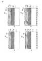
まず、本発明の反射型マスクブランクの構成について説明する。図1(a)〜(d)は、本発明の反射型マスクブランク100、200、300、400の断面を示している。即ち、本発明のブランクの構成は、100、200、300、400のいずれを用いてもよい。図2は、図1(a)〜(d)の本発明の反射型マスクブランク100、200、300、400を上面から見た図である。 First, the configuration of the reflective mask blank of the present invention will be described. 1A to 1D show cross sections of the reflective mask blanks 100, 200, 300, and 400 of the present invention. That is, any of 100, 200, 300, and 400 may be used for the blank structure of the present invention. FIG. 2 is a top view of the
図1(a)に示す反射型マスクブランク100は、基板11の表面に、多層反射層21、吸収層51が順次形成されている。図1(b)に示す反射型マスクブランク200は、基板11の表面に、多層反射層21、吸収層51が順次形成されていると共に、基板11の裏面に導電膜71が形成された構造となっている。つまり、図1(b)の反射型マスクブランク200は、図1(a)の反射型マスクブランク100の基板11の裏面に導電膜71が形成されている。図1(c)の反射型マスクブランク300は、基板11の表面に多層反射層21、緩衝層41、吸収層51が順次形成されている。図1(d)の反射型マスクブランク400は、図1(c)の反射型マスクブランク300の基板11の裏面に導電膜71が形成された構造となっている。 In the reflective mask blank 100 shown in FIG. 1A, a multilayer
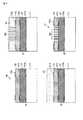
前記基板11の多層反射層側の表面で、後にチップ周辺部の遮光枠に相当する領域には、微細な凹凸パターンが形成された凹凸領域11aが存在しており、次いで形成された多層反射層21には多層反射層の凹凸領域21aが、次いで形成された吸収層51には、吸収層の凹凸領域51aが形成されている。図1(c)、(d)の場合は、緩衝層41の凹凸領域41aも形成されている。図1(a)〜(d)の反射型マスクブランク100、200、300、400を上面から見ると図2のように、通常の吸収層領域80と遮光枠領域90が形成されている。 On the surface of the
ここで、前記基板11の凹凸領域11aの凹凸パターンについて説明する。即ち、基板11は、後にパターン周辺部の遮光枠領域となる部分が、高さ2.5〜4.5nm、周期30nm以下の凹凸領域11aを有している。基板11の凹凸領域11aの凹凸は、ドット、ホール、ライン&スペースのいずれでも良い。また、上述した高さと周期の条件を満たせば、ランダムな配置であっても良い。 Here, the uneven pattern of the
次に、前記基板11に凹凸領域11aを形成する方法について説明する。まず、図1に示す基板11を用意し、その表面に対し、リソグラフィ、エッチング、レジスト剥離洗浄工程を経て、基板11の凹凸領域11aを形成する。このときのパターンの周期が30nm以下であれば、パターンの種類はドット、ホール、ライン&スペースのいずれでも良い。 Next, a method for forming the
エッチングの掘り込み深さは、2.5〜4.5nmになるように、エッチング条件と処理時間を設定する。エッチング方法は、ウェットエッチングであればエッチング液にフッ酸を用い、ドライエッチングであれば、基板のエッチングに適している塩素、フッ素、臭素、ヨウ素等のハロゲン原子を含むガスを用いたプラズマエッチング法が可能である。 Etching conditions and processing time are set so that the etching depth is 2.5 to 4.5 nm. For wet etching, hydrofluoric acid is used as an etchant, and for dry etching, plasma etching using a gas containing a halogen atom such as chlorine, fluorine, bromine, or iodine, which is suitable for etching a substrate. Is possible.
また、基板11に凹凸領域11aを形成する別の方法としては、凹凸領域となる部分の基板表面に自己組織化単分子膜(Self-Assembled Monolayers:SAM)によって、周期30nm以下のドットパターンを形成し、次いでSAMをエッチングマスクとしてドライエッチングにより、基板11に深さ2.5〜4.5nmの凹凸パターンを形成しても良い。 As another method for forming the
さらに、基板11に凹凸領域11aを形成する別の方法としては、上述したようなリソグラフィや自己組織化単分子膜による所望の周期や大きさを有する微細パターン(後にエッチングマスクとなるもの)を形成せずに、基板に直接プラズマやウェット処理をすることで、表面にラフネスを形成しても良い。リソグラフィや自己組織化単分子膜に比べ、パターンの周期や大きさなどの制御性は、低いが、周期30nm以下、且つ深さ2.5〜4.5nmの凹凸パターンは、エッチング条件と時間を適宜設定して形成することも可能である。ただし、この場合、凹凸領域以外の領域は、エッチングによって処理されないように保護される必要があるので、あらかじめリソグラフィやフィルムにより保護膜を形成しておく。 Furthermore, as another method for forming the
また、さらに基板11に凹凸領域11aを形成する別の方法としては、基板11に対して直接サンドブラスト処理を施すことによって所望の周期や高さを有するラフネスを形成しても良い。ただし、この場合も、凹凸領域以外の領域は、サンドブラストによって処理されないように保護される必要があるので、あらかじめリソグラフィやフィルムにより保護膜を形成しておく。 Further, as another method of forming the
次に、基板以外のブランクの構成(多層反射層21、緩衝層41、吸収層51、裏面導電膜71)について説明する。これらの膜は、いずれもスパッタリング法により形成する。 Next, the configuration of the blank other than the substrate (the multilayer
このうち、図1(a)、(b)の多層反射層21は、13.5nm近傍のEUV光に対して60%程度の反射率を達成できるように設計されており、モリブデン(Mo)とシリコン(Si)が交互に40〜50ペア積層した積層膜で、さらに最上層はルテニウム(Ru)で構成されている。Ru層の下に隣接する層はSi層である。MoやSiが使われている理由は、EUV光に対する吸収(消衰係数)が小さく、且つMoとSiのEUV光での屈折率差が大きいために、SiとRuの界面での反射率を高く出来るためである。多層反射層の最上層のRuは、吸収層の加工におけるストッパーやマスク洗浄時の薬液に対する保護層としての役割を果たしている。 Among these, the multilayer
そして、図1(c)、(d)の多層反射層21は、13.5nm近傍のEUV光に対して60%程度の反射率を達成できるように設計されており、MoとSiが交互に40〜50ペア積層した積層膜で、最上層はSi層で構成されている。この場合の多層反射層の最上層のSiも、上述したRuと同様の役割を果たす。 The multilayer
また、図1(c)、(d)の緩衝層41は、吸収層51のエッチングやパターン修正時に、緩衝層の下に隣接する多層反射層21の最上層であるSi層を保護するために設けられており、クロム(Cr)の窒素化合物(CrN)で構成されている。 In addition, the
そして、図1(a)〜(d)の吸収層51は、13.5nm近傍のEUVに対して吸収率の高いタンタル(Ta)の窒素化合物(TaN)で構成されている。他の材料として、タンタルホウ素窒化物(TaBN)、タンタルシリコン(TaSi)、タンタル(Ta)や、それらの酸化物(TaBON、TaSiO、TaO)でも良い。 The absorbing
そして、図1(a)〜(d)の吸収層51は、上層に波長190〜260nmの紫外光に対して反射防止機能を有する低反射層を設けた2層構造から成る吸収層であっても良い。低反射層は、マスクの欠陥検査機の検査波長に対して、コントラストを高くし、検査性を向上させるためのものである。 1 (a) to 1 (d) is an absorption layer having a two-layer structure in which a low reflection layer having an antireflection function with respect to ultraviolet light having a wavelength of 190 to 260 nm is provided on the upper layer. Also good. The low reflection layer is for increasing the contrast and improving the inspection property with respect to the inspection wavelength of the mask defect inspection machine.
また、図1(b)及び図1(d)の導電膜71は、一般にはCrNで構成されているが、導電性があれば良いので、金属材料からなる材料であれば良い。 In addition, the
前記反射型マスクブランク100,200,300,400は、基板11の凹凸領域11aが形成された表面に、スパッタリング法により多層反射層21、吸収層51、緩衝層41が形成されるため、基板11の凹凸領域11aの凹凸形状は、最上層の吸収層51まで引き継がれる。したがって、多層反射層21、吸収層51、緩衝層41それぞれの凹凸領域21a、51a、41aは、別段の処理をしなくとも、自動的に形成される。 In the
ここで、重要なことは、基板11の凹凸形状によって、多層反射層21にも同様の高さ2.5〜4.5nm、周期30nm以下の凹凸形状が形成されることである。これによって、EUV光を露光し、反射されるEUV光の位相が凹凸の凹部と凸部でほぼ180度反転するために、打ち消しあい、反射率を大幅に低下させることが可能となる。本来、凹凸部の高低差は、EUV光の波長13.5nmの1/4波長の奇数倍(3.375nm、10.125nm、16.875nm)で、丁度180度反転する計算になるが、実験によれば、概ね2.5〜4.5nmの範囲で充分な効果が見られた。周期に関しては、EUV波長13.5nmにおいて、反転した位相が効果を発揮する距離を、周期を振った実験によって調べたところ、概ね30nm以下で効果が見られた。 Here, what is important is that a similar uneven shape having a height of 2.5 to 4.5 nm and a period of 30 nm or less is also formed in the multilayer
次に、この発明の一実施の形態に係る反射型マスク及びその製造方法について詳細に説明する。 Next, a reflective mask and a manufacturing method thereof according to an embodiment of the present invention will be described in detail.
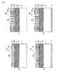
ここで、図3(a)には、前記図1(a)の反射型マスクブランク100から作製した反射型マスク101を示し、図3(b)には、前記図1(b)の反射型マスクブランク200から作製した反射型マスク201を示す。そして、図3(c)には、前記図1(c)の反射型マスクブランク300から作製した反射型マスク301を示し、図3(d)には、前記図1(d)の反射型マスクブランク400から作製した反射型マスク401を示す。いずれも、多層反射層21の上部の吸収層51及び緩衝層41がある場合は緩衝層41を掘り込むことによって、回路パターン領域85を有する反射型マスクが形成される。これら図3(a)〜(d)の反射型マスク101、201、301、401は,いずれも図4に示すように通常の吸収層領域80と遮光枠領域90と回路パターン領域85から構成されている。 Here, FIG. 3 (a) shows a
このようにして、EUV光に対する反射率が吸収層領域80よりも充分に小さい遮光枠領域90を有する反射型マスクブランクを得る。 In this way, a reflective mask blank having a light
ここで、上記反射マスクを作製する場合には、まず、図1に示す反射型マスクブランク100もしくは200を用意し、電子線リソグラフィによりレジストパターンを形成後、フルオロカーボンプラズマもしくは塩素プラズマ、必要な場合はその両方のプラズマより吸収層51をエッチングし、レジスト剥離洗浄することで、吸収層51に回路パターン領域85を形成して図3に示す反射型マスク101もしくは201を作製する。 Here, when producing the reflective mask, first, the reflective mask blank 100 or 200 shown in FIG. 1 is prepared, and after forming a resist pattern by electron beam lithography, fluorocarbon plasma or chlorine plasma, if necessary. The
また、図1に示す反射型マスクブランク300もしくは400を用意し、電子線リソグラフィによりレジストパターンを形成後、フルオロカーボンプラズマもしくは塩素プラズマ、必要な場合はその両方のプラズマより吸収層51をエッチングし、次いで塩素プラズマにより緩衝層41をエッチングし、レジスト剥離洗浄することで、吸収層51および緩衝層41に回路パターン領域85を形成して図3(a)に示す反射型マスク301もしくは401を作製する。 Also, a reflective mask blank 300 or 400 shown in FIG. 1 is prepared, and after forming a resist pattern by electron beam lithography, the absorbing
このようにして、EUV光に対する反射率が吸収層領域よりも充分に小さい遮光枠領域を有する反射型マスク101,201,301,401を作製する。 In this way, the
次に、本願発明による実施例1として反射型マスクブランクを作成し、実施例2として実施例1で作製した反射型マスクブランクを用いて反射型マスクを作製して、その特性を確認する。 Next, a reflective mask blank is produced as Example 1 according to the present invention, and a reflective mask blank is produced using the reflective mask blank produced in Example 1 as Example 2, and its characteristics are confirmed.
(実施例1)
図5(a)に示すように基板として低熱膨張ガラス基板111を用意して、後に遮光枠となる領域(チップ外周部を取り囲むように幅2mmの帯状の領域)に、電子線レジスト131(ZEP520、日本ゼオン製)を膜厚20nmでコートする(図5(b)参照)。次に、EB描画機(JBX9000、日本電子製)により、ドーズ100μC/cm2で、パターン線幅15nm、周期30nmのパターンを描画し、有機現像によりレジストドットパターン131aを形成した(図5(c)参照)。Example 1
As shown in FIG. 5A, a low thermal
続いて、CF4/Ar混合ガスプラズマによるドライエッチングと、残ったレジストの剥膜洗浄を経て、基板111の一部にドットからなる凹凸パターン111aを形成する(図5(d)参照)。 Subsequently, a concavo-
次に、波長13.5nmのEUV光に対して反射率が64%程度となるように設計されたMoとSiの40ペアの積層及び最上層にRuをもつ多層反射層121とTaNからなる吸収層151をスパッタリング装置により順次形成する(図5(d)、(e)参照)。このときの吸収層151の膜厚は、50nmとした。このようにして、外周部に遮光領域90(図2参照)を有する反射型マスクブランク100が完成される(図5(f)参照)。 Next, an absorption layer composed of 40 pairs of Mo and Si designed to have a reflectance of about 64% with respect to EUV light having a wavelength of 13.5 nm and a multilayer
そして、この実施例1にて作製した反射型マスクブランク100の吸収層側のEUV光(波長13.5nm)の反射率を測定した。この結果、遮光枠以外の領域(通常の吸収層部)での反射率が1.24%であるのに対し、遮光枠領域(遮光枠部)の反射率が0.21%となり、遮光枠以外に比べて、概ね1/6に低減していることが確認された(図6参照)。網掛け
(実施例2)
実施例1にて作製した反射型マスクブランク100から反射型マスク101を作製し、露光テストを図7に示す手順で実施した。即ち、反射型マスクブランク100に電子線リソグラフィとドライエッチング、レジスト剥離洗浄を行い、吸収層151に回路パターン185を形成し、本発明の遮光枠を有する反射型マスク101を作製した。電子線リソグラフィには、化学増幅型ポジレジストFEP171(富士フィルムエレクトニクスマテリアルズ製)を用いて、描画機JBX9000(日本電子製)によってドーズ15μC/cm描画した後に、TMAH2.38%現像液によりレジストパターン184を形成した(図7(c)参照)。吸収層51のエッチングには、Cl2の誘導結合型プラズマを適用した。And the reflectance of the EUV light (wavelength 13.5 nm) by the side of the absorption layer of the reflective mask blank 100 produced in this Example 1 was measured. As a result, the reflectance of the region other than the light shielding frame (normal absorption layer portion) is 1.24%, whereas the reflectance of the light shielding frame region (light shielding frame portion) is 0.21%. Compared to other cases, it was confirmed that the ratio was reduced to 1/6 (see FIG. 6). Shading (Example 2)
A
そして、この実施例2にて作製した反射型マスク101を用いて13.5nmのEUVを光源とした露光を行い、半導体基板上に隣接した4つのチップを転写した。隣接したチップにおいて、作製した反射型マスク上の遮光枠に相当する領域の一部は重なっていたにもかかわらず、半導体基板上の当該領域におけるレジストの感光は確認されなかった。 Then, using the
本発明は、上記実施の形態に限ることなく、その他、実施段階ではその要旨を逸脱しない範囲で種々の変形を実施し得ることが可能である。さらに、上記実施形態には、種々の段階の発明が含まれており、開示される複数の構成要件における適宜な組合せにより、種々の発明が抽出され得る。 The present invention is not limited to the above-described embodiment, and various modifications can be made without departing from the scope of the invention at the stage of implementation. Furthermore, the above embodiments include inventions at various stages, and various inventions can be extracted by appropriately combining a plurality of disclosed constituent elements.
例えば実施形態に示される全構成要件から幾つかの構成要件が削除されても、発明が解決しようとする課題の欄で述べた課題が解決でき、発明の効果で述べられている効果が得られる場合には、この構成要件が削除された構成が発明として抽出され得る。 For example, even if some constituent elements are deleted from all the constituent elements shown in the embodiment, the problems described in the column of problems to be solved by the invention can be solved, and the effects described in the effects of the invention can be obtained. In some cases, a configuration from which this configuration requirement is deleted can be extracted as an invention.
本発明によれば、遮光枠の形成において、マスク作製時のリソグラフィ、エッチングなどによるパターニング工程を必要とせず、且つ欠陥面でのマスク品質低下を防ぎ、且つ吸収層へのダメージや光学的性質の変化のない、遮光性の高い遮光枠を有する反射型マスクブランク及びその製造方法、反射型マスク及びその製造方法を提供することができる。 According to the present invention, the formation of the light-shielding frame does not require a patterning step by lithography, etching, or the like at the time of mask production, prevents deterioration of the mask quality on the defective surface, and damages to the absorption layer or optical properties. It is possible to provide a reflective mask blank having a light-shielding frame having a high light-shielding property and a method for manufacturing the same, a reflective mask, and a method for manufacturing the same.
11・・・基板
11a・・・基板の凹凸領域
21・・・多層反射層
21a・・・多層反射層の凹凸領域
41・・・緩衝層
41a・・・緩衝層の凹凸領域
51・・・吸収層
51a・・・吸収層の凹凸領域
71・・・裏面導電膜
80・・・非遮光枠領域
85・・・回路パターン領域
90・・・遮光枠領域
100、200、300、400・・・反射型マスクブランク
101、201、301、401・・・反射型マスク
111・・・低熱膨張基板
111a・・・低熱膨張基板の凹凸領域
121・・・多層反射層
121a・・・多層反射層の凹凸領域
151・・・吸収層
151a・・・吸収層の凹凸領域
131・・・基板の凹凸パターン形成のためのレジスト
131a・・・基板の凹凸パターン形成のためのレジストパターン
161・・・回路パターン形成のためのレジスト
184・・・回路パターン形成のためのレジストパターン
185・・・吸収枠の回路パターンDESCRIPTION OF
Claims (11)
Translated fromJapanese前記低熱膨張基板表面に形成された多層反射層と、
前記多層反射層の上に形成された吸収層と、
を具備し、前記吸収層には転写回路パターンが形成され、ブランク作製時に前記転写回路パターン領域の外側にEUV光の反射率の低い遮光枠を設けることを特徴とする反射型マスクブランク。A low thermal expansion substrate;
A multilayer reflective layer formed on the surface of the low thermal expansion substrate;
An absorbing layer formed on the multilayer reflective layer;
The reflective mask blank is characterized in that a transfer circuit pattern is formed on the absorption layer, and a light-shielding frame having a low EUV light reflectance is provided outside the transfer circuit pattern region when the blank is manufactured.
前記多層反射層を形成する工程に先だって、凹凸形状を形成する工程と、
を具備することを特徴とする反射型マスクブランクの製造方法。Forming a multilayer reflective layer on the surface of the low thermal expansion substrate in the region that will later become a light shielding frame;
Prior to the step of forming the multilayer reflective layer, a step of forming a concavo-convex shape,
The manufacturing method of the reflective mask blank characterized by comprising.
Priority Applications (1)
| Application Number | Priority Date | Filing Date | Title |
|---|---|---|---|
| JP2011043883AJP5742300B2 (en) | 2011-03-01 | 2011-03-01 | REFLECTIVE MASK BLANK AND ITS MANUFACTURING METHOD, REFLECTIVE MASK |
Applications Claiming Priority (1)
| Application Number | Priority Date | Filing Date | Title |
|---|---|---|---|
| JP2011043883AJP5742300B2 (en) | 2011-03-01 | 2011-03-01 | REFLECTIVE MASK BLANK AND ITS MANUFACTURING METHOD, REFLECTIVE MASK |
Publications (2)
| Publication Number | Publication Date |
|---|---|
| JP2012182289Atrue JP2012182289A (en) | 2012-09-20 |
| JP5742300B2 JP5742300B2 (en) | 2015-07-01 |
Family
ID=47013243
Family Applications (1)
| Application Number | Title | Priority Date | Filing Date |
|---|---|---|---|
| JP2011043883AExpired - Fee RelatedJP5742300B2 (en) | 2011-03-01 | 2011-03-01 | REFLECTIVE MASK BLANK AND ITS MANUFACTURING METHOD, REFLECTIVE MASK |
Country Status (1)
| Country | Link |
|---|---|
| JP (1) | JP5742300B2 (en) |
Cited By (4)
| Publication number | Priority date | Publication date | Assignee | Title |
|---|---|---|---|---|
| JP2016012598A (en)* | 2014-06-27 | 2016-01-21 | 凸版印刷株式会社 | Reflective phase shift mask and method for manufacturing the same |
| JP2018025716A (en)* | 2016-08-12 | 2018-02-15 | 凸版印刷株式会社 | Reflective exposure mask and method of manufacturing the same |
| JP2018044979A (en)* | 2016-09-12 | 2018-03-22 | 大日本印刷株式会社 | Reflective mask and method of manufacturing the same |
| JP2023167983A (en)* | 2022-05-13 | 2023-11-24 | 信越化学工業株式会社 | Reflective photomask blank and manufacturing method of reflective photomask |
Citations (18)
| Publication number | Priority date | Publication date | Assignee | Title |
|---|---|---|---|---|
| JPH01152725A (en)* | 1987-12-10 | 1989-06-15 | Toshiba Corp | Method for manufacturing an X-ray exposure mask |
| JPH0588355A (en)* | 1991-09-25 | 1993-04-09 | Canon Inc | Reflection type mask and exposure device using the same |
| JPH05134385A (en)* | 1991-11-11 | 1993-05-28 | Nikon Corp | Reflective mask |
| JPH06124876A (en)* | 1992-10-12 | 1994-05-06 | Hitachi Ltd | Optical element and method of manufacturing optical element |
| JPH09232203A (en)* | 1996-02-20 | 1997-09-05 | Canon Inc | Reflective X-ray mask structure, X-ray exposure apparatus, X-ray exposure method, and device manufactured using the reflective X-ray mask structure |
| US6514877B1 (en)* | 1999-10-27 | 2003-02-04 | Universite De Sherbrooke | Method using sub-micron silicide structures formed by direct-write electron beam lithography for fabricating masks for extreme ultra-violet and deep ultra-violet lithography |
| US20060134556A1 (en)* | 2004-11-22 | 2006-06-22 | Wisconsin Alumni Research Foundation | Methods and compositions for forming aperiodic patterned copolymer films |
| JP2007220732A (en)* | 2006-02-14 | 2007-08-30 | Matsushita Electric Ind Co Ltd | X-ray lithography mask, method for producing the same, method for producing anti-reflection structure using the same, and method for producing a mold, glass molding, or resin molding using the anti-reflection structure |
| US20080076035A1 (en)* | 2006-09-21 | 2008-03-27 | Pei-Yang Yan | Phase shift mask structure and fabrication process |
| US20090148781A1 (en)* | 2007-12-07 | 2009-06-11 | Takashi Kamo | Reflective-type mask |
| WO2009122972A1 (en)* | 2008-03-31 | 2009-10-08 | Hoya株式会社 | Reflection type mask blank, reflection type mask, and method for manufacturing the same |
| JP2009229657A (en)* | 2008-03-21 | 2009-10-08 | Asahi Kasei E-Materials Corp | Photosensitive resin composition and laminated body |
| WO2009136564A1 (en)* | 2008-05-09 | 2009-11-12 | Hoya株式会社 | Reflective mask, reflective mask blank and method for manufacturing reflective mask |
| JP2009262546A (en)* | 2008-03-31 | 2009-11-12 | Toray Ind Inc | Method and apparatus for manufacturing fine pattern-transfer sheet |
| US20100289182A1 (en)* | 2007-09-28 | 2010-11-18 | Yuma Hirai | method and device for manufacturing sheet having fine shape transferred thereon |
| US20100297559A1 (en)* | 2008-03-21 | 2010-11-25 | Yosuke Hata | Photosensitive resin composition, photosensitive resin laminate, method for forming resist pattern and process for producing printed circuit board, lead frame, semiconductor package and concavoconvex board |
| US20100304277A1 (en)* | 2009-05-26 | 2010-12-02 | Hynix Semiconductor Inc. | Photomask for Extreme Ultraviolet Lithography and Method for Fabricating the Same |
| JP2012054412A (en)* | 2010-09-01 | 2012-03-15 | Dainippon Printing Co Ltd | Reflective mask with light blocking region, reflective mask blank, method of manufacturing reflective mask |
- 2011
- 2011-03-01JPJP2011043883Apatent/JP5742300B2/ennot_activeExpired - Fee Related
Patent Citations (23)
| Publication number | Priority date | Publication date | Assignee | Title |
|---|---|---|---|---|
| JPH01152725A (en)* | 1987-12-10 | 1989-06-15 | Toshiba Corp | Method for manufacturing an X-ray exposure mask |
| JPH0588355A (en)* | 1991-09-25 | 1993-04-09 | Canon Inc | Reflection type mask and exposure device using the same |
| JPH05134385A (en)* | 1991-11-11 | 1993-05-28 | Nikon Corp | Reflective mask |
| US5399448A (en)* | 1991-11-11 | 1995-03-21 | Nikon Corporation | Reflection mask for X ray |
| JPH06124876A (en)* | 1992-10-12 | 1994-05-06 | Hitachi Ltd | Optical element and method of manufacturing optical element |
| JPH09232203A (en)* | 1996-02-20 | 1997-09-05 | Canon Inc | Reflective X-ray mask structure, X-ray exposure apparatus, X-ray exposure method, and device manufactured using the reflective X-ray mask structure |
| US6514877B1 (en)* | 1999-10-27 | 2003-02-04 | Universite De Sherbrooke | Method using sub-micron silicide structures formed by direct-write electron beam lithography for fabricating masks for extreme ultra-violet and deep ultra-violet lithography |
| JP2008520450A (en)* | 2004-11-22 | 2008-06-19 | ウィスコンシン・アラムナイ・リサーチ・ファウンデーション | Method and composition for non-periodic pattern copolymer films |
| US20060134556A1 (en)* | 2004-11-22 | 2006-06-22 | Wisconsin Alumni Research Foundation | Methods and compositions for forming aperiodic patterned copolymer films |
| JP2007220732A (en)* | 2006-02-14 | 2007-08-30 | Matsushita Electric Ind Co Ltd | X-ray lithography mask, method for producing the same, method for producing anti-reflection structure using the same, and method for producing a mold, glass molding, or resin molding using the anti-reflection structure |
| US20080076035A1 (en)* | 2006-09-21 | 2008-03-27 | Pei-Yang Yan | Phase shift mask structure and fabrication process |
| US20100289182A1 (en)* | 2007-09-28 | 2010-11-18 | Yuma Hirai | method and device for manufacturing sheet having fine shape transferred thereon |
| US20090148781A1 (en)* | 2007-12-07 | 2009-06-11 | Takashi Kamo | Reflective-type mask |
| JP2009141223A (en)* | 2007-12-07 | 2009-06-25 | Toshiba Corp | Reflective mask |
| JP2009229657A (en)* | 2008-03-21 | 2009-10-08 | Asahi Kasei E-Materials Corp | Photosensitive resin composition and laminated body |
| US20100297559A1 (en)* | 2008-03-21 | 2010-11-25 | Yosuke Hata | Photosensitive resin composition, photosensitive resin laminate, method for forming resist pattern and process for producing printed circuit board, lead frame, semiconductor package and concavoconvex board |
| WO2009122972A1 (en)* | 2008-03-31 | 2009-10-08 | Hoya株式会社 | Reflection type mask blank, reflection type mask, and method for manufacturing the same |
| JP2009262546A (en)* | 2008-03-31 | 2009-11-12 | Toray Ind Inc | Method and apparatus for manufacturing fine pattern-transfer sheet |
| US20110027703A1 (en)* | 2008-03-31 | 2011-02-03 | Hoya Corporation | Reflective mask blank, reflective mask, and method of manufacturing the same |
| WO2009136564A1 (en)* | 2008-05-09 | 2009-11-12 | Hoya株式会社 | Reflective mask, reflective mask blank and method for manufacturing reflective mask |
| US20110059391A1 (en)* | 2008-05-09 | 2011-03-10 | Hoya Corporation | Reflective mask, reflective mask blank and method of manufacturing reflective mask |
| US20100304277A1 (en)* | 2009-05-26 | 2010-12-02 | Hynix Semiconductor Inc. | Photomask for Extreme Ultraviolet Lithography and Method for Fabricating the Same |
| JP2012054412A (en)* | 2010-09-01 | 2012-03-15 | Dainippon Printing Co Ltd | Reflective mask with light blocking region, reflective mask blank, method of manufacturing reflective mask |
Cited By (6)
| Publication number | Priority date | Publication date | Assignee | Title |
|---|---|---|---|---|
| JP2016012598A (en)* | 2014-06-27 | 2016-01-21 | 凸版印刷株式会社 | Reflective phase shift mask and method for manufacturing the same |
| JP2018025716A (en)* | 2016-08-12 | 2018-02-15 | 凸版印刷株式会社 | Reflective exposure mask and method of manufacturing the same |
| JP7005129B2 (en) | 2016-08-12 | 2022-01-21 | 凸版印刷株式会社 | Reflective exposure mask |
| JP2018044979A (en)* | 2016-09-12 | 2018-03-22 | 大日本印刷株式会社 | Reflective mask and method of manufacturing the same |
| JP2023167983A (en)* | 2022-05-13 | 2023-11-24 | 信越化学工業株式会社 | Reflective photomask blank and manufacturing method of reflective photomask |
| JP7687269B2 (en) | 2022-05-13 | 2025-06-03 | 信越化学工業株式会社 | Reflective photomask blank and method for manufacturing a reflective photomask |
Also Published As
| Publication number | Publication date |
|---|---|
| JP5742300B2 (en) | 2015-07-01 |
Similar Documents
| Publication | Publication Date | Title |
|---|---|---|
| CN103858210B (en) | Reflective mask base, reflective mask and their manufacture method | |
| WO2013027412A1 (en) | Reflective mask and method for manufacturing same | |
| JP5953833B2 (en) | Reflective photomask and method of manufacturing the same | |
| JP6287046B2 (en) | Reflective mask, reflective mask blank and manufacturing method thereof | |
| JP5742300B2 (en) | REFLECTIVE MASK BLANK AND ITS MANUFACTURING METHOD, REFLECTIVE MASK | |
| JP5790073B2 (en) | Method for manufacturing a reflective mask blank | |
| JP5990961B2 (en) | Reflective mask | |
| JP2014090132A (en) | Reflective mask and manufacturing method thereof | |
| JP5909964B2 (en) | Reflective mask blank and reflective mask | |
| JP6260149B2 (en) | Reflective mask blank and reflective mask | |
| JP6070109B2 (en) | Reflective mask and method of manufacturing the same | |
| JP5884565B2 (en) | Reflective mask and method of manufacturing the same | |
| JP5970901B2 (en) | REFLECTIVE MASK AND METHOD FOR PRODUCING REFLECTIVE MASK | |
| JP2014232844A (en) | Method for manufacturing reflective mask | |
| JP2014183075A (en) | Reflective mask, and method of manufacturing the same | |
| JP5754592B2 (en) | Reflective mask manufacturing method and reflective mask | |
| JP5796307B2 (en) | Reflective mask blank and manufacturing method thereof | |
| JP5970910B2 (en) | Method for manufacturing a reflective mask | |
| JP5803517B2 (en) | Reflective mask, mask blank, and manufacturing method thereof | |
| JP2015141972A (en) | Euv mask and method of manufacturing euv mask | |
| JP2016134472A (en) | REFLECTIVE MASK BLANK, ITS MANUFACTURING METHOD, AND REFLECTIVE MASK | |
| US20170306475A1 (en) | Reflective mask, reflective mask blank, and manufacturing method therefor | |
| JP2017227702A (en) | Reflective photomask | |
| US9921465B2 (en) | Reflective mask, reflective mask blank and manufacturing method therefor | |
| JP2015035529A (en) | Reflective mask |
Legal Events
| Date | Code | Title | Description |
|---|---|---|---|
| A621 | Written request for application examination | Free format text:JAPANESE INTERMEDIATE CODE: A621 Effective date:20140219 | |
| A977 | Report on retrieval | Free format text:JAPANESE INTERMEDIATE CODE: A971007 Effective date:20140924 | |
| A131 | Notification of reasons for refusal | Free format text:JAPANESE INTERMEDIATE CODE: A131 Effective date:20141007 | |
| A521 | Written amendment | Free format text:JAPANESE INTERMEDIATE CODE: A523 Effective date:20141205 | |
| TRDD | Decision of grant or rejection written | ||
| A01 | Written decision to grant a patent or to grant a registration (utility model) | Free format text:JAPANESE INTERMEDIATE CODE: A01 Effective date:20150407 | |
| A61 | First payment of annual fees (during grant procedure) | Free format text:JAPANESE INTERMEDIATE CODE: A61 Effective date:20150420 | |
| R150 | Certificate of patent or registration of utility model | Ref document number:5742300 Country of ref document:JP Free format text:JAPANESE INTERMEDIATE CODE: R150 | |
| LAPS | Cancellation because of no payment of annual fees |