JP2012174790A - Semiconductor device and manufacturing method of the same - Google Patents
Semiconductor device and manufacturing method of the sameDownload PDFInfo
- Publication number
- JP2012174790A JP2012174790AJP2011033431AJP2011033431AJP2012174790AJP 2012174790 AJP2012174790 AJP 2012174790AJP 2011033431 AJP2011033431 AJP 2011033431AJP 2011033431 AJP2011033431 AJP 2011033431AJP 2012174790 AJP2012174790 AJP 2012174790A
- Authority
- JP
- Japan
- Prior art keywords
- insulating film
- film
- semiconductor
- groove
- semiconductor device
- Prior art date
- Legal status (The legal status is an assumption and is not a legal conclusion. Google has not performed a legal analysis and makes no representation as to the accuracy of the status listed.)
- Ceased
Links
Images


Classifications
- H—ELECTRICITY
- H10—SEMICONDUCTOR DEVICES; ELECTRIC SOLID-STATE DEVICES NOT OTHERWISE PROVIDED FOR
- H10B—ELECTRONIC MEMORY DEVICES
- H10B12/00—Dynamic random access memory [DRAM] devices
- H10B12/01—Manufacture or treatment
- H10B12/02—Manufacture or treatment for one transistor one-capacitor [1T-1C] memory cells
- H10B12/05—Making the transistor
- H10B12/053—Making the transistor the transistor being at least partially in a trench in the substrate
- H—ELECTRICITY
- H10—SEMICONDUCTOR DEVICES; ELECTRIC SOLID-STATE DEVICES NOT OTHERWISE PROVIDED FOR
- H10B—ELECTRONIC MEMORY DEVICES
- H10B12/00—Dynamic random access memory [DRAM] devices
- H10B12/30—DRAM devices comprising one-transistor - one-capacitor [1T-1C] memory cells
- H10B12/48—Data lines or contacts therefor
- H10B12/485—Bit line contacts
Landscapes
- Engineering & Computer Science (AREA)
- Manufacturing & Machinery (AREA)
- Semiconductor Memories (AREA)
Abstract
Translated fromJapaneseDescription
Translated fromJapanese本発明は、半導体装置及びその製造方法に関する。 The present invention relates to a semiconductor device and a manufacturing method thereof.
近年、半導体装置の高集積化、高性能化に伴い、半導体装置の配線ピッチは益々縮小され、さらなる縮小が求められている。そしてこれに伴い、克服すべき課題が生じている。例えば、半導体装置の一例であるDRAM(Dynamic Random Access Memory)では、配線ピッチの縮小に伴い、メモリセルにおいて、活性領域とビット線コンタクトとの間の接触面積が縮小化され、これに伴うコンタクト抵抗の増大の問題が発生している。
特に、活性領域がビット線及びワード線に対して交差する方向に延在する構成(例えば、特許文献1)では、活性領域とビット線コンタクトとの間の接触面積の縮小が顕著である。In recent years, with the high integration and high performance of semiconductor devices, the wiring pitch of semiconductor devices has been increasingly reduced, and further reduction is required. Along with this, problems to be overcome have arisen. For example, in a DRAM (Dynamic Random Access Memory) which is an example of a semiconductor device, a contact area between an active region and a bit line contact is reduced in a memory cell as a wiring pitch is reduced, and a contact resistance associated therewith is reduced. The problem of increasing is occurring.
In particular, in a configuration in which the active region extends in a direction intersecting the bit line and the word line (for example, Patent Document 1), the reduction of the contact area between the active region and the bit line contact is significant.
特許文献2には、活性領域がビット線の延在方向に対して平行に配置される構成で、活性領域をT字形状にしてT字の凸部分の上面にビット線コンタクトをコンタクトさせることにより、活性領域若しくは不純物拡散領域とビット線コンタクトとの間の接触面積の増大を図り、コンタクト抵抗を低下させる方法が開示されている。 In
しかしながら、活性領域がビット線に延在する方向に平行な構成であっても、活性領域をT字形状にする上記構成ではT字の凸部分のためにDRAMの高集積化を十分に達成できないという問題があった。 However, even if the active region is parallel to the direction extending to the bit line, the above-described configuration in which the active region is T-shaped cannot sufficiently achieve high integration of DRAM due to the T-shaped convex portion. There was a problem.
そこで、本発明は、以下の構成を採用した。
本発明に係る半導体装置は、半導体基板の主面に形成された第1の方向に直線状に延在する複数の第1の溝と、前記第1の溝の下部を埋めこんで形成された第2の絶縁層からなる素子分離領域と、前記半導体基板の主面に形成された第1の方向に直交する第2の方向に直線状に延在する複数の第2の溝と、前記第2の溝の下部を埋め込んで、該第2の溝の内壁上の第5の絶縁膜を介して第2の溝内に形成されたワード線と、前記第1の溝と前記第2の溝とによって前記半導体基板内に区画して形成され、前記半導体基板の主面に対して垂直方向に立設すると共に、上部に活性領域たる不純物拡散領域を有する複数の半導体ピラーと、第1の方向に並ぶ所定数ごとの半導体ピラーにその前記上部の側面を介して前記不純物拡散領域に電気的に接続すると共に、前記第2の絶縁層上に形成されたビット線コンタクトと、第1の方向に直線状に延在し、前記ビット線コンタクトに電気的に接続するビット線と、を備えることを特徴とする。Therefore, the present invention employs the following configuration.
A semiconductor device according to the present invention is formed by embedding a plurality of first grooves formed linearly in a first direction formed on a main surface of a semiconductor substrate and a lower portion of the first grooves. An element isolation region made of a second insulating layer; a plurality of second grooves extending linearly in a second direction perpendicular to the first direction formed on the main surface of the semiconductor substrate; A word line formed in the second groove through the fifth insulating film on the inner wall of the second groove, and the first groove and the second groove. A plurality of semiconductor pillars that are partitioned in the semiconductor substrate and are erected in a direction perpendicular to the main surface of the semiconductor substrate and having an impurity diffusion region as an active region on the upper side, and a first direction Are electrically connected to the impurity diffusion regions via the upper side surfaces of a predetermined number of semiconductor pillars arranged in a row And a bit line contact formed on the second insulating layer, and a bit line extending linearly in the first direction and electrically connected to the bit line contact. To do.
以上のように、本発明は、直線状に並んで配置する活性領域が直線状に並んで配置するビット線と平行な構成であって、ビット線コンタクトが活性領域の半導体ピラーの上部の不純物拡散領域の側面に接触することにより電気的なコンタクトをとる構成なので、従来技術のようにビット線コンタクトを形成するために活性領域をT字状に形成していた構成が不要となりメモリセルの微細化を図ることが可能となる。また、活性領域の側面にコンタクトを形成する構成となるので、平面的な活性領域の面積を増大することなく、活性領域(不純物拡散領域)とビット線コンタクトとの間の接触面積を増大させることが可能となり、コンタクト抵抗の低下を図ることができる。また、本発明は、トランジスタのゲート電極となるワード線が溝内に埋め込まれており半導体基板表面より上方に突出していない。
且つ、ビット線を活性領域に平行に延在する構成としていることからビット線が活性領域を横切らない構成となっており、微細化された状態でもストレージノードコンタクトとなる活性領域の上面の面積を最大限確保することができストレージノードコンタクトの抵抗を低減することができる。As described above, according to the present invention, the active region arranged in a straight line has a configuration parallel to the bit line arranged in a straight line, and the bit line contact is an impurity diffusion above the semiconductor pillar in the active region. Since the contact is made by making contact with the side surface of the region, the configuration in which the active region is formed in a T shape to form the bit line contact as in the prior art becomes unnecessary, and the memory cell is miniaturized. Can be achieved. Further, since the contact is formed on the side surface of the active region, the contact area between the active region (impurity diffusion region) and the bit line contact can be increased without increasing the area of the planar active region. Thus, the contact resistance can be reduced. Further, according to the present invention, the word line that becomes the gate electrode of the transistor is buried in the trench and does not protrude above the surface of the semiconductor substrate.
In addition, since the bit line is configured to extend in parallel with the active region, the bit line does not cross the active region, and the area of the upper surface of the active region that becomes the storage node contact is reduced even in a miniaturized state. As much as possible, the resistance of the storage node contact can be reduced.
以下に、本発明を適用した一実施形態である半導体装置及びその製造方法について、図
面を適宜参照しながら説明する。本実施形態においては、半導体装置の一例として、DRAM(Dynamic Random Access Memory)に、本発明を適用した場合を例に挙げて説明する。なお、以下の説明において参照する図面は、本実施形態の半導体装置の製造方法を説明する図面であって、図示される各部の大きさや厚さや寸法等は、実際の半導体装置等の寸法関係とは異なっていることがある。また、以下の説明において例示する材料や寸法等は一例であり、本発明はそれらに必ずしも限定されるものではなく、その要旨を変更しない範囲で適宜変更して実施することが可能である。
以下の実施形態では、実施例を併せて説明するが、具体的に示した材料や寸法等の条件は例示に過ぎない。Hereinafter, a semiconductor device according to an embodiment to which the present invention is applied and a manufacturing method thereof will be described with reference to the drawings as appropriate. In the present embodiment, a case where the present invention is applied to a DRAM (Dynamic Random Access Memory) will be described as an example of a semiconductor device. The drawings to be referred to in the following description are drawings for explaining the method of manufacturing the semiconductor device of the present embodiment, and the size, thickness, dimensions, etc. of each part shown in FIG. May be different. In addition, the materials, dimensions, and the like exemplified in the following description are examples, and the present invention is not necessarily limited thereto, and can be appropriately modified and implemented without departing from the scope of the invention.
In the following embodiments, examples will be described together, but the specific conditions such as materials and dimensions are merely examples.
まず、図1A〜図1Cに示す本発明を適用した半導体装置の一例である半導体記憶装置(DRAM)の構造について説明する。図示した構造は半導体装置の一部を示すものである。
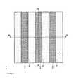
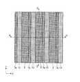
なお、図1Aはこの半導体装置100の一部を示す平面レイアウトを示す図である。その内部の構造も一部示している。図1Bは図1Aで示す半導体装置100の切断線A−Aによる断面図、図1Cは図1Aで示す半導体装置100の切断線B−Bによる断面図である。First, a structure of a semiconductor memory device (DRAM) which is an example of a semiconductor device to which the present invention shown in FIGS. 1A to 1C is applied will be described. The structure shown shows a part of the semiconductor device.
FIG. 1A is a diagram showing a planar layout showing a part of the
この半導体装置100は、最終的にDRAMとして機能させるものであり、各メモリセルはソース又はドレイン領域(不純物拡散領域)23a、23b、及びゲート電極(ワード線)17を有するMOSトランジスタと、キャパシタ40とを有する。
図1Aにおいてはキャパシタ40の位置を示しているが、図1Bにおいては省略している。
なお、本実施形態で説明する半導体装置(DRAM)100は、図1Aに示すように、6F2(2F×3F)セル配置(Fは最小加工寸法)とされている。The
Although the position of the
The semiconductor device (DRAM) 100 described in the present embodiment has a 6F2 (2F × 3F) cell arrangement (F is a minimum processing dimension) as shown in FIG. 1A.
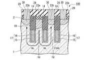
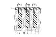
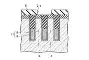
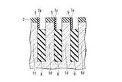
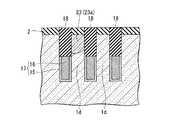
この半導体装置100は、半導体基板1の主面に形成されたy方向(第1の方向)に直線状に延在する複数の素子分離溝(第1の溝)4と、素子分離溝4の下部を埋めこんで形成された素子分離領域(第2の絶縁層)6と、半導体基板1の主面に形成されたy方向に直交するx方向(第2の方向)に直線状に延在する複数のワード線形成溝(第2の溝)14と、ワード線形成溝14の下部を埋めこんで、ワード線形成溝14の内壁上のゲート絶縁膜(第5の絶縁膜;図示せず)を介してワード線形成溝14内に形成されたワード線17と、素子分離溝4とワード線形成溝14とによって半導体基板1内に区画して形成され、半導体基板1の主面に対して垂直方向に立設すると共に、上部に不純物拡散領域23を有する複数の半導体ピラー1dと、y方向に並ぶ3個ごと(3個目ごと)の半導体ピラー1dにその上部の側面を介して不純物拡散領域23aに電気的に接続すると共に、素子分離領域6上に形成されたビット線コンタクト22aと、x方向に直線状に延在し、ビット線コンタクト22aに電気的に接続するビット線26と、を備える。 The
上述の、y方向に並ぶ3個ごとの半導体ピラー1dについて以下に説明する。
図1Aを参照すると、y方向にはWL(ワード線17)が等ピッチ間隔で4本配置されている。図の右側に記載されているように、下に配置されたWLと、上に配置されたWLは、FSWL(Field Shield Word Line)となっており、y方向に延在する活性領域を電気的に分離するための素子分離領域として設けられている。上下の2本のFSWLに挟まれて配置された2本のWLがトランジスタのゲート電極およびワード線として機能するものである。FSWLは、WLと同一構成で形成されるが、トランジスタのゲート電極およびワード線としては機能しない。FSWLは、いわゆるダミーWLとなる。ここで、ビット線コンタクトは、2本のWLに挟まれた半導体ピラー1d(図1Aにおいて、上下方向の中央に位置する半導体ピラー)の側面に接触して形成される。DRAMのメモリセルでは、図1Aに示したWL、WL、FSWLの3本のWLが単位構成となってy方向に繰り返し配置される。具体的には、WL、WL、FSWL、WL、WL、FSWLの順に配置される。各WLおよびFSWLの間には半導体ピラーが位置している。ビット線コンタクトはWL、WL間の半導体ピラーに対して形成されるので、y方向には半導体ピラーの3個に1個の割合で、ビット線コンタクトが形成された半導体ピラー1dが出現することとなる。The above-described three
Referring to FIG. 1A, four WLs (word lines 17) are arranged at equal pitch intervals in the y direction. As shown in the right side of the figure, the WL arranged below and the WL arranged above are FSWL (Field Shield Word Line), and the active region extending in the y direction is electrically connected. It is provided as an element isolation region for isolation. Two WLs arranged between two upper and lower FSWLs function as a gate electrode and a word line of the transistor. FSWL is formed with the same structure as WL, but does not function as a gate electrode or a word line of a transistor. The FSWL is a so-called dummy WL. Here, the bit line contact is formed in contact with the side surface of the
説明を戻すと、この半導体装置100は、上記の上部に不純物拡散領域23aを有する複数の半導体ピラー1d以外の半導体ピラーにおいてはその上面を介してその不純物拡散領域23bに電気的に接続するストレージノードコンタクト30と、ストレージノードコンタクト30に電気的に接続するキャパシタ40と、を備える。
本実施形態では、3個ごと(3個目ごと)の半導体ピラー1dにその上部の側面を介して不純物拡散領域23aにビット線コンタクト22aが電気的に接続する構成であるが、他の個数とすることもできる。Returning to the description, the
In the present embodiment, the
半導体基板1は、所定濃度の不純物を含有する基板、例えばp型単結晶シリコン基板からなり、この半導体基板1の面内のうち、素子分離溝(第1の溝)4の下部を第2の絶縁層が埋め込まれて形成された素子分離領域6はこの場合、STI(Shallow Trench Isolation)と呼ばれる構造であり、素子形成領域はこの素子分離領域(第2の絶縁層)6によって絶縁分離された活性領域である。したがって、活性領域は、y方向に延在する各々の素子分離領域6によって挟まれ、素子分離領域6と同じy方向に延在する半導体基板1で構成される。素子分離溝(第1の溝)4の深さは、ワード線形成溝(第2の溝)14の深さに対して1.3〜2.0倍深くなるように形成される。好ましくは1.6倍とする。
本発明に係る半導体装置の製造方法で記載する実施例は、半導体基板1としてp型シリコン基板を用いた場合について説明する。The
In the embodiment described in the method for manufacturing a semiconductor device according to the present invention, a case where a p-type silicon substrate is used as the
また、各素子形成領域には、x方向(第2の方向)及びy方向(第1の方向)のそれぞれに対して平行にマトリックス状に配置する半導体ピラー1dが複数並んで半導体基板1の主面に対して垂直方向に立設している。半導体ピラー1dの上部には不純物拡散領域23(23a、23b)を有する。
不純物拡散領域には、ビット線コンタクト22aに接続する不純物拡散領域23aと、ストレージノードコンタクト30に接続する不純物拡散領域23bとがある。In each element formation region, a plurality of
The impurity diffusion region includes an
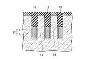
また、半導体基板1には、素子分離領域(第2の絶縁層)6及び素子形成領域1a(図2C参照)を形成した後に形成され、素子形成領域1aに交差する方向であるx方向に直線状に延在するワード線形成溝(第2の溝)14を有する。
ワード線形成溝(第2の溝)14にはその下部にワード線17が埋め込まれ、その上に第6の絶縁膜18が形成されている。In addition, the
A
ワード線17には、実際にトランジスタを動作させる機能を有するワード線WLと、トランジスタを動作させる機能を有さずに、素子分離の機能を有するFSWLとがある。
すなわち、埋め込みワード線WLと埋め込みワード線(素子分離)FSWLとは同一の構造を有しているが、機能が異なっている。ここで、埋め込みワード線WLがメモリセルのゲート電極として用いられるのに対して、素子分離用のFSWLは、所定の電位をかけて隣接するトランジスタ間を分離するために設けられている。すなわち、同一の活性領域上で隣接するトランジスタ間は、素子分離用の埋め込みワード線FSWLを所定の電位に維持することで、寄生トランジスタをオフ状態として分離することができる。The
That is, the embedded word line WL and the embedded word line (element isolation) FSWL have the same structure, but different functions. Here, the embedded word line WL is used as the gate electrode of the memory cell, whereas the element isolation FSWL is provided to isolate adjacent transistors by applying a predetermined potential. In other words, the parasitic transistors can be separated from each other adjacent transistors on the same active region by maintaining the embedded word line FSWL for element isolation at a predetermined potential.
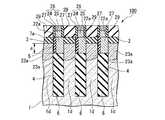
また、半導体装置100は、x方向に直交するy方向に直線状に延在するビット線(BL)26を有する。ビット線(BL)26はビット線コンタクト22aを介して半導体ピラー1dの上部の不純物拡散領域23aに電気的に接続されている。
ビット線(BL)26は不純物をドープしたポリシリコン層24と、窒化タングステン(WN)膜とタングステン(W)膜とを順次堆積させることによりW/WN膜(メタル膜)25との積層構造からなる。ビット線(BL)26の側面はシリコン窒化膜からなるサイドウォール絶縁膜27によって覆われている。隣接するビット線(BL)26の側面を覆うサイドウォール絶縁膜27の間は、ストレージノードコンタクト30を形成するためのマスクとして用いられたシリコン酸化膜からなる絶縁膜29で埋め込まれている。ビット線(BL)26と隣接するストレージノードコンタクト30は、ビット線の側壁に形成されたサイドウォール絶縁膜27を介して相互に絶縁されている。In addition, the
The bit line (BL) 26 has a laminated structure of a W / WN film (metal film) 25 by sequentially depositing a
図1Cを参照すると、第2の方向(x方向)には、ビット線コンタクト22aが接続される半導体ピラー1dが等ピッチ間隔で複数配置されている。各々の半導体ピラー1dの間にはx方向の素子分離領域となる第1の溝4が設けられている。視点を変えると、一つの第1の溝4の両側に接して、それぞれ半導体ピラー1dが設けられている。第1の溝4の下部には素子分離絶縁膜6が埋め込まれている。素子分離絶縁膜6上にはビット線コンタクト22aが設けられている。ビット線コンタクト22aは、第1の溝4に隣接する両側の半導体ピラー1dの内、一方の半導体ピラーの表面を含む上部の側面と接触して設けられている。他の一方の半導体ピラーに対しては、当該半導体ピラーの側面に酸化膜5を介して形成されたサイドウォール絶縁膜(第3の絶縁膜)7aによって絶縁されている。各々の半導体ピラー1dの上面には第1の絶縁膜2が設けられており、ビット線コンタクトプラグ22aは、素子分離絶縁膜6の上面を底面とし、接続される側の半導体ピラーと第1の絶縁膜2の側面を一方の側壁とし、他の一方の側壁を対向するサイドウォール絶縁膜7aとして構成される溝を埋め込んで設けられている。これによって、ビット線コンタクト22aは、半導体ピラー1dの上部側面と接続される。ビット線コンタクト22aの上面は、各々の半導体ピラーの上面に設けられた第1の絶縁膜の上面と面一となっている。複数のビット線コンタクト22aは、第1の方向に延在する各々の活性領域(半導体ピラー1d)間に位置しており、各々のビット線コンタクト22aの上面を接続して第1の方向に延在するビット線26が設けられている。したがって、各々のビット線26は、各々直線で構成される活性領域の間に位置して、活性領域と平行な第1の方向に延在する直線で構成される。
ビット線コンタクト22aの底面は、埋め込みワード線17の上面よりも浅い位置、すなわち埋め込みワード線17の上面よりも半導体基板表面側に位置するように設けることが望ましい。Referring to FIG. 1C, in the second direction (x direction), a plurality of
The bottom surface of the
以上のように、本発明の半導体装置では、上部に不純物拡散領域23を有する半導体ピラー1dが素子分離溝(第1の溝)4によって区画されており、この第1の溝4の下部を埋めこんで素子分離領域(第2の絶縁層)6が形成され、この素子分離領域6の上には素子分離溝(第1の溝)4を埋め込む厚さでビット線コンタクト22aが形成されている。この構成とすることにより、ビット線コンタクト22aは不純物拡散領域23とその側面で接触することになるため、素子分離溝(第1の溝)4に埋め込まれるビット線コンタクト22aの厚さ(深さ)d1(図1C)を適切にとることにより、ビット線コンタクト22aは不純物拡散領域23との接触面積を増大させ、コンタクト抵抗を低下させることができる。
素子分離溝(第1の溝)4に埋め込まれるビット線コンタクト22aの厚さ(深さ)d1は、半導体基板1の主面から25nm程度であるのが望ましい。
また、ビット線26を活性領域23(23a、23b)に平行に延在する構成としていることからビット線26が活性領域23(23a、23b)を横切らない構成となっている。したがって、微細化された状態でもストレージノードコンタクト30と接触する活性領域23bの上面と、ビット線26およびビット線サイドウォール絶縁膜27とを重ならないように構成することができ、ストレージノードコンタクト30と接触する活性領域23bの上面の面積を最大限確保することができストレージノードコンタクトの抵抗を低減することができる。
さらに、図1Cに示したように、本実施例ではビット線をポリシリコン層24とメタル層25との2層構成としているが、下層のポリシリコン層24を省いて、メタル層25だけで構成することもできる。この構成とすれば、ビット線自体の高さを低減でき、ビット線より上方に形成される構造物の加工を容易化できる効果がある。As described above, in the semiconductor device of the present invention, the
The thickness (depth) d1 of the
In addition, since the
Further, as shown in FIG. 1C, in this embodiment, the bit line has a two-layer structure of the
なお、素子形成領域には、実際はメモリセルが多数並んで形成されているものの、図1A〜図1Cに示す半導体装置100では、これらのメモリセルを全て図示することが困難なことから、便宜上、素子形成領域内においてメモリセルの数を減らした状態で模式的に示している。 Note that although a large number of memory cells are actually formed in the element formation region, in the
以上のような半導体装置100の動作の例を説明すると、図1Bに矢印によって摸式的に示すように、ビット線26からビット線コンタクト22aへ流れた電流はビット線コンタクト22aから半導体ピラー1dの上部の側面を介して不純物拡散領域23aへ流れ、矢印に沿ってワード線17の側面に沿って形成されたチャネルを通って隣接する半導体ピラー1dの上部の不純物拡散領域23bへ流れ、さらにストレージノードコンタクト30を介してキャパシタ40へ流れ込んでキャパシタ40に電荷が蓄積される。 Explaining an example of the operation of the
(半導体装置の製造方法)
次に、本発明を適用した半導体装置の一例である半導体記憶装置(DRAM)の製造方法について図2〜図20を参照して説明する。
図2A〜図20Aは各製造工程における平面レイアウトを示す図である。図2B〜図20Bはそれぞれ、図2A〜図20Aのそれぞれの切断線A−Aによる断面図、図2C〜図20Cはそれぞれ、図2A〜図20Aのそれぞれの切断線B−Bによる断面図である。
なお、以下の説明では、上記半導体装置100と同等の部位については、説明を省略すると共に、図面において同じ符号を付すものとする。(Method for manufacturing semiconductor device)
Next, a method for manufacturing a semiconductor memory device (DRAM) as an example of a semiconductor device to which the present invention is applied will be described with reference to FIGS.
2A to 20A are diagrams showing a planar layout in each manufacturing process. 2B to 20B are cross-sectional views taken along the cutting line AA of FIGS. 2A to 20A, respectively. FIGS. 2C to 20C are cross-sectional views taken along the cutting lines BB of FIGS. 2A to 20A, respectively. is there.
In the following description, portions equivalent to those of the
(素子分離溝の形成工程)
まず、図2A〜図2Cに示すように、半導体基板1の面内に、第1の絶縁膜2を用いてy方向(第1の方向)に直線状に延在する複数の素子分離溝(第1の溝)4をx方向(第2の方向)に離間して並ぶように形成すると共に、これによって隣接する素子分離溝4間に素子形成領域1aを形成する。素子分離溝4は素子分離領域を埋め込むことによって素子分離領域となり、隣接する素子分離領域間に形成された素子形成領域1aは素子形成領域となる。この素子分離領域はこの場合、STIと呼ばれる構造であり、素子形成領域は素子分離領域によって絶縁分離された活性領域である。
半導体基板1に素子分離溝4を設けるには、半導体基板1上に、マスク用の絶縁膜(第1の絶縁膜)2を堆積し、フォトリソグラフィ技術およびドライエッチング技術を用いて、マスク用絶縁膜2、半導体基板1のパターニングを順次行ない、半導体基板1に素子形成領域1a(もしくは活性領域)を区画するための素子分離溝(第1の溝)4を形成する。
素子分離溝(第1の溝)4は素子形成領域1aで挟まれた部位だけでなく、素子形成領域1a上に形成されたマスク用の絶縁膜(第1の絶縁膜)2で挟まれた部位まで含む。(Element isolation trench formation process)
First, as shown in FIGS. 2A to 2C, a plurality of element isolation trenches (linearly extending in the y direction (first direction) using the first insulating
In order to provide the
The element isolation trench (first trench) 4 is sandwiched not only by the portion sandwiched by the
具体的には例えば、P型のシリコン基板からなる半導体基板1上に、CVD法によってマスク用のシリコン窒化膜(第1の絶縁膜)2を堆積し、フォトリソグラフィ技術およびドライエッチング技術を用いて、シリコン窒化膜2、半導体基板1のパターニングを順次行ない、半導体基板1に活性領域1aを区画するためのSTI素子分離溝(トレンチ)4を形成する。STI素子分離溝(トレンチ)4で区画された活性領域1aは素子形成領域からなる。活性領域1aとなる領域は図1A〜図1Cに示すように、マスク用のシリコン窒化膜2で覆われている。 Specifically, for example, a silicon nitride film (first insulating film) 2 for masking is deposited on a
(素子分離溝の充填工程)
次に、図3A〜図3Cに示すように、素子分離溝(第1の溝)4に、素子形成領域1aの上部側面1cが露出されたままとするように、素子分離溝4の下部を埋めこんで第2の絶縁膜6を形成する。(Element isolation groove filling process)
Next, as shown in FIGS. 3A to 3C, the lower portion of the
具体的には例えば、素子分離溝4の内面を含む全面にCVD法によってシリコン酸窒化膜(絶縁膜)を形成して、素子分離溝4をシリコン酸窒化膜6で埋め込む。次いで、熱燐酸にてシリコン酸窒化膜(第2の絶縁膜)6を選択的にエッチバックして、シリコン酸窒化膜6の上面が半導体基板(シリコン基板)1の上面から25nm程度下になる(図3C中の深さd1が25nm程度になる)ように露出させる。次いで、熱酸化(ISSG:In Situ Steam Generation)により酸化させることによって、露出されたシリコン基板面(上部側面)1c、及びシリコン窒化膜(第1の絶縁膜)2の表面に厚さ4nm程度の酸化膜5を形成する。ISSGによる酸化はラジカル酸化なので、ほぼ選択比なしで酸化することができる。 Specifically, for example, a silicon oxynitride film (insulating film) is formed on the entire surface including the inner surface of the
(片側サイドウォールの形成工程)
次に、素子形成領域1aの、y方向(第1の方向)に平行な一対の上部側面1c(1ca、1cb)のうち一方の上部側面1ca上にのみ、第1の溝4の下部を埋めこんで第3の絶縁膜7aを形成する。
以下に、この工程の一例について、図3〜図9を用いて詳細に説明する。(Side side wall formation process)
Next, the lower portion of the
Below, an example of this process is demonstrated in detail using FIGS.
(サイドウォールの形成工程)
まず、図4A〜図4Cに示すように、素子形成領域1aのy方向(第1の方向)に平行な一対の上部側面1ca、1cbのそれぞれに、酸化膜5を介して絶縁膜のサイドウォール(第3の絶縁膜)7(7a、7b)を形成する。(Sidewall formation process)
First, as shown in FIGS. 4A to 4C, the sidewalls of the insulating film are formed on the pair of upper side surfaces 1 ca and 1 cb parallel to the y direction (first direction) of the
具体的には例えば、素子分離溝4の内面を含む全面にCVD法によってシリコン窒化膜を形成した後、エッチバックしてマスク用絶縁膜2上のシリコン窒化膜を除去して、素子形成領域1aのy方向に平行な一対の一対の上部側面1ca、1cbに酸化膜5を介してシリコン窒化膜からなるサイドウォール7(7a、7b)を形成する。 Specifically, for example, after a silicon nitride film is formed on the entire surface including the inner surface of the
(凹部(リセス)の形成工程)
次に、図5A〜図5Cに示すように、素子分離溝(第1の溝)4内に第3の絶縁膜7(7a、7b)と異なる材料からなる第8の絶縁膜8を、第3の絶縁膜7(7a、7b)の上面7aa、7baより低くなるように形成して、素子分離溝4内の第8の絶縁膜8上に凹部9を形成する。(Process for forming recesses)
Next, as shown in FIGS. 5A to 5C, an eighth
具体的には例えば、素子分離溝4の内面を含む全面にCVD法によってシリコン酸化膜(第3の絶縁膜)を形成した後、ドライエッチングを用いてこのシリコン酸化膜(第3の絶縁膜)をシリコン窒化膜(第1の絶縁膜)2上のシリコン酸化膜(素子分離溝4の内面を含む全面にCVD法によって上記シリコン酸化膜のうち、シリコン窒化膜(第1の絶縁膜)2上のシリコン酸化膜については図示省略)の上面からの深さd2を、例えば30nm程度までエッチバックして素子分離溝4内のそのシリコン酸化膜(第3の絶縁膜)8の上方に凹部(リセス)9を形成するように、シリコン酸化膜8を素子分離溝4内に形成する。
この工程により、素子分離溝4内のシリコン酸窒化膜6上のシリコン酸化膜(第8の絶縁膜)8上に、サイドウォール7a及び7bに囲まれた凹部9が形成される。Specifically, for example, a silicon oxide film (third insulating film) is formed on the entire surface including the inner surface of the
By this step, the
(片側サイドウォール形成用マスクの形成工程)
次に、まず、図6A〜図6Cに示すように、凹部9の下部を埋めこんで、凹部9を含む全面に第2の半導体膜10を形成する。すなわち、素子分離溝4の内面を含む全面に、素子分離溝4内の下部を埋めこんで、素子形成領域1aの一対の上部側面1cのうちの一方の上部側面(片側)1caにサイドウォールを形成するためのマスク用の第2の半導体膜10を形成する。(Process for forming a mask for forming one side wall)
Next, as shown in FIGS. 6A to 6C, the
具体的には例えば、素子分離溝4の内面を含む全面に、CVD法により、成膜温度を540℃以下として厚さ10nm程度のアモルファスシリコン膜(第2の半導体膜)10を形成する。アモルファスシリコン膜(第2の半導体膜)10は、素子形成領域1aの上部側面(素子分離溝4内の内壁)に形成された部分(側面アモルファスシリコン膜)10a、10cと、素子分離溝4内の第3の絶縁膜8上に形成された部分(水平アモルファスシリコン膜)10bと、シリコン窒化膜2上にシリコン酸化膜(図示省略)を介して形成された部分(上面アモルファスシリコン膜)10dとからなる。アモルファスシリコンはエッチング段階で、不均一なエッチングが生じる原因となる結晶粒の影響が現れないという利点がある。
図6A〜図6Cに示した工程により、素子分離溝4内のシリコン酸窒化膜6上には、素子形成領域1aの上部側面1ca上に酸化膜5を介してサイドウォール7aと、上部側面1cb上に酸化膜5を介してサイドウォール7bと、シリコン酸化膜(第8の絶縁膜)8と、シリコン酸化膜(第8の絶縁膜)8上に側面アモルファスシリコン膜10a、水平アモルファスシリコン膜10b及び側面アモルファスシリコン膜10cとが形成される。Specifically, for example, an amorphous silicon film (second semiconductor film) 10 having a thickness of about 10 nm is formed on the entire surface including the inner surface of the
6A to 6C, on the
次に、図7A〜図7Cに示すように、第2の半導体膜10にその垂直方向に対して傾いた角度から不純物を注入した後、湿式エッチングを施して、第2の半導体膜10のうち、一方の上部側面1caと反対側の上部側面1cb上の第3の絶縁膜7bを介して形成されている第2の半導体膜の部分10cと、第8の絶縁膜8上の第2の半導体膜の部分10bの一部とを除去する。 Next, as shown in FIGS. 7A to 7C, after the impurity is implanted into the
具体的には例えば、アモルファスシリコン膜10のうち、一方の側面アモルファスシリコン膜10a(図6Cにおいて左側のアモルファスシリコン膜の部分)と、水平アモルファスシリコン膜10bの一部(図6Cにおいて底部に形成されたアモルファスシリコン膜の部分のうち、左側半分程度)と、上面アモルファスシリコン膜10dとに、図7Cに矢印で示す方向から不純物を注入して、側面アモルファスシリコン膜の一方である(図6Cにおいて右側のアモルファスシリコン膜の部分)10cと水平アモルファスシリコン膜10bの一部(図6Cにおいて底部に形成されたアモルファスシリコン膜の部分のうち、右側半分)とを除去する。
アモルファスシリコン膜10に添加される不純物としてはフッ化ボロン(BF2)などが挙げられる。側面アモルファスシリコン膜10a、10cのうち一方の側面アモルファスシリコン膜10cに不純物を注入せずに、上面アモルファスシリコン膜10dと側面アモルファスシリコン膜10aと水平アモルファスシリコン膜10bの一部とに不純物を添加する方法としては、例えば、斜めイオン注入法などが挙げられる。図7Cにおいては、斜めイオン注入法を用いて、アモルファスシリコン膜10に不純物を注入する場合を例に挙げて示している。Specifically, for example, the
An example of the impurity added to the
また、図7Cにおいてアモルファスシリコン膜10に不純物を注入する場合、側面アモルファスシリコン膜10aだけでなく、水平アモルファスシリコン膜10bの一部にも不純物を添加する必要がある。このため、アモルファスシリコン膜10に不純物を注入する方法として、側面アモルファスシリコン膜10a及び水平アモルファスシリコン膜10bの各部位に最適な注入角度となるように、角度の異なる2段階注入法を用いてもよい。ここで、注入角度とは、半導体基板1の表面に対する垂線からの傾斜角を意味している。 7C, when impurities are implanted into the
2段階注入法を用いてアモルファスシリコン膜10に不純物を注入する場合、例えば、加速エネルギー5keV、注入ドーズ量2E14cm−2で、注入角度20°での注入と注入角度30°での注入とを組み合わせることが好ましい。なお、注入角度は、アモルファスシリコン膜10の膜厚や、水平アモルファスシリコン膜10bの面積、側面アモルファスシリコン膜10a、10cの深さなどに応じて適宜変更できる。In the case of implanting impurities into the
不純物の注入されていないアモルファスシリコン膜10の一部(すなわち、側面アモルファスシリコン膜の一方である(図7Cにおいて右側のアモルファスシリコン膜の部分)10c及び水平アモルファスシリコン膜10bの一部(図7Cにおいて底部に形成されたアモルファスシリコン膜の部分のうち、右側半分))を除去するには、アンモニア水(NH3)などをエッチング液として用いたウェットエッチングを実施する。A part of the
図7A〜図7Cに示した工程により、素子分離溝4内のシリコン酸窒化膜6上には、素子形成領域1aの上部側面1ca上に酸化膜5を介してサイドウォール7aと、上部側面1cb上に酸化膜5を介してサイドウォール7bと、シリコン酸化膜(第8の絶縁膜)8と、シリコン酸化膜(第8の絶縁膜)8上に側面アモルファスシリコン膜10aとが残る。 7A to 7C, on the
(一方のサイドウォールの除去工程)
次に、図8A〜図8Cに示すように、素子形成領域1aの一対の上部側面1ca、1cbのうち、上部側面1cb上の第3の絶縁膜7bを除去する。すなわち、素子分離溝4の上部の露出面に酸化膜5を介して両側に形成されているサイドウォール7a,7bのうち、第2の半導体膜10のマスクに覆われてない片側のサイドウォール7b(図8Cにおいて右側のサイドウォール)を除去する。(Step of removing one side wall)
Next, as shown in FIGS. 8A to 8C, the third
具体的には例えば、熱燐酸(H3PO4)を用いたウェットエッチングにより、アモルファスシリコン膜10のマスクに覆われてない片側のサイドウォール7bを除去する。サイドウォール7aはアモルファスシリコン膜10のマスク及びシリコン酸化膜(第3の絶縁膜)8に覆われているため、このウェットエッチングの際に、除去されずに、素子形成領域1aの上部側面1ca上に残る。
この工程により、素子分離溝4内のシリコン酸窒化膜6上には、素子形成領域1aの上部側面1ca上に酸化膜5を介してサイドウォール7aと、シリコン酸化膜(第8の絶縁膜)8と、側面アモルファスシリコン膜10aとが残る。Specifically, for example, the
By this step, the
(第8の絶縁膜の除去工程)
次に、図9A〜図9Cに示すように、素子分離溝4内の第8の絶縁膜8を除去する。(Eighth insulating film removal step)
Next, as shown in FIGS. 9A to 9C, the eighth insulating
具体的には例えば、フッ酸(HF)を用いたウェットエッチングにより、シリコン酸窒化膜(絶縁膜)6上のシリコン酸化膜(第8の絶縁膜)8を除去する。
この工程により、素子分離溝4内のシリコン酸窒化膜6上には、素子形成領域1aの上部側面1ca上に酸化膜5を介してサイドウォール7aと、側面アモルファスシリコン膜10aとが残る。Specifically, for example, the silicon oxide film (eighth insulating film) 8 on the silicon oxynitride film (insulating film) 6 is removed by wet etching using hydrofluoric acid (HF).
By this step, the
(片側サイドウォール形成用マスクの除去工程)
次に、図10A〜図10Cに示すように、片側サイドウォール形成用マスクである第2の半導体膜10を除去する。(Removal process of the side wall forming mask)
Next, as shown in FIGS. 10A to 10C, the
具体的には例えば、異方性エッチングによりエッチバックして、片側サイドウォール形成用マスクであるアモルファスシリコン膜10を除去する。
この工程により、素子分離溝4内のシリコン酸窒化膜6上には、素子形成領域1aの上部側面1ca上に酸化膜5を介してサイドウォール7aが残る。Specifically, for example, the
By this step, the
以上の工程により、素子分離溝4内のシリコン酸窒化膜6上にシリコン窒化膜からなる片側サイドウォール7aを形成することができる。 Through the above steps, the one-
(素子分離溝の充填及び平坦化工程)
次に、図11A〜図11Cに示すように、素子分離溝(第1の溝)4を埋め込むように、第3の絶縁膜7aと異なる材料からなる第4の絶縁膜13を形成する。この素子分離溝4を絶縁膜で充填することによって、素子分離溝4内で露出していた素子形成領域1aの側面1cbのシリコン面を保護する。(Element isolation trench filling and planarization process)
Next, as shown in FIGS. 11A to 11C, a fourth insulating
具体的には例えば、素子分離溝(第1の溝)4の内面を含む全面にHDP−CVD(High Density Plasma−Chemical Vapor Deposition)法により、サイドウォール7aの材料であるシリコン窒化膜と異なる材料からなるシリコン酸化膜(第4の絶縁膜)13を成膜した後、化学的機械研磨(CMP:Chemical Mechanical Polishing)により研磨しながら、シリコン窒化膜2の表面が露出するまで平坦化を行い、素子分離溝(第1の溝)4を埋め込むシリコン酸化膜(第4の絶縁膜)13を形成する。
この工程により、素子分離溝4内は、素子形成領域1aの上部側面1ca上に酸化膜5を介してサイドウォール7aと、シリコン酸化膜(第4の絶縁膜)13とによって充填される。Specifically, for example, a material different from the silicon nitride film which is the material of the
By this step, the
(埋込ワード線の形成工程)
次に、まず、図12A〜図12Cに示すように、半導体基板1の面内にy方向(第1の方向)に直交するx方向(第2の方向)に直線状に延在する複数のワード線WLの形成溝(第2の溝)14が離間して並ぶように形成すると共に、これによって素子形成領域1aをx方向で分離して複数の半導体ピラー1dを形成する。(Embedded word line formation process)
Next, first, as shown in FIGS. 12A to 12C, a plurality of linearly extending in the x direction (second direction) orthogonal to the y direction (first direction) in the plane of the
具体的には例えば、マスク用のシリコン窒化膜及びカーボン膜(アモルファス・カーボン膜)を順次堆積し、x方向(第2の方向)に延在すると共にy方向(第1の方向)に離間して並ぶワード線形成溝14のパターンにパターニングする。次いで、ドライエッチングによってシリコン基板1をエッチングし、ワード線形成溝14を形成する。ワード線形成溝14は、活性領域1aと交差する第1の方向(x方向)に延在するライン状のパターンとして形成される。
この工程により、活性領域(素子形成領域)1aは、素子分離溝4とワード線形成溝14とによって半導体基板1内に区画して形成され、半導体基板1の主面に対して垂直方向に立設する半導体ピラー1dごとに分離される。Specifically, for example, a silicon nitride film for mask and a carbon film (amorphous carbon film) are sequentially deposited and extend in the x direction (second direction) and are separated in the y direction (first direction). Patterning is performed in a pattern of the word
Through this process, the active region (element formation region) 1 a is formed in the
次に、図13A〜図13Cに示すように、ワード線形成溝(第2の溝)14内の下部にワード線形成溝14の内壁に形成した第5の絶縁膜(図示せず)を介してワード線17を形成する。 Next, as shown in FIGS. 13A to 13C, a fifth insulating film (not shown) formed on the inner wall of the word
具体的には例えば、ワード線形成溝(第2の溝)14の内壁を覆うように、ゲート酸化膜(第5の絶縁膜)を例えば、4nm程度の膜厚で形成する。この際、ゲート酸化膜(図示せず)としては、例えば、ワード線形成溝14の内面表層を、ISSG(In Situ Steam Generation)によって熱酸化することによって形成する。
次に、ワード線形成溝14内のゲート酸化膜(第5の絶縁膜)上にゲート(ワード線)材料として、例えば、窒化チタン(TiN)層15をワード線形成溝14の下部側面及び底面に形成し、この窒化チタン(TiN)層15上にタングステン(W)層16を堆積させることにより、ワード線形成溝14の下部にTiN/Wの積層膜17を形成する。
次に、TiN/Wの積層膜の上部を、通常のドライエッチング等の方法でエッチバックして除去することにより、TiN/Wの積層膜17をワード線形成溝14の底部に残存した状態で形成してワード線17を形成する。
図13A〜図13Cに示した工程により、ワード線形成溝14の下部にワード線17が形成される。Specifically, for example, a gate oxide film (fifth insulating film) is formed with a film thickness of about 4 nm so as to cover the inner wall of the word line formation groove (second groove) 14. At this time, the gate oxide film (not shown) is formed, for example, by thermally oxidizing the inner surface layer of the word
Next, for example, a titanium nitride (TiN)
Next, the upper portion of the TiN / W laminated film is removed by etching back by a method such as ordinary dry etching, so that the TiN / W laminated
13A to 13C, the
ここで、ワード線17は、埋め込みワード線WLと埋め込みワード線(素子分離)FSWLとがあり、これらは同一の構造を有しているが、機能が異なっている。ここで、埋め込みワード線WLがメモリセルのゲート電極として用いられるのに対して、素子分離用のFSWLは、所定の電位をかけて隣接するトランジスタ間を分離するために設けられている。隣接するトランジスタとの素子分離は、STI構造を用いるのが一般的であるが、本実施形態に係る半導体装置では、y方向に隣接する素子間は素子分離領域6によって分離され、x方向に隣接する素子間は埋め込みゲート電極によって分離される。ここで、トランジスタの埋め込みワード線WLと素子分離用の埋め込みワード線FSWLは、同時形成が可能であることから公知のダブルパターニング技術が適用でき、さらなる微細化に好適な構造であることが知られている。 Here, the
次に、図14A〜図14Cに示すように、ワード線形成溝(第2の溝)14内のワード線17上に第6の絶縁膜18を形成する。 Next, as shown in FIGS. 14A to 14C, a sixth insulating
具体的には例えば、TiN/Wの積層膜17上及びワード線形成溝14の内壁を覆うように、CVD法によってシリコン窒化膜からなる埋込絶縁膜(第6の絶縁膜)18を形成する。
次に、CMPを行って表面を平坦化し、埋込絶縁膜(第6の絶縁膜)18の表面が、マスク用絶縁膜2の表面と概略同程度の高さになるようにする。
図14A〜図14Cに示した工程により、埋込ワード線が完成する。Specifically, for example, a buried insulating film (sixth insulating film) 18 made of a silicon nitride film is formed by a CVD method so as to cover the TiN / W laminated
Next, CMP is performed to flatten the surface so that the surface of the buried insulating film (sixth insulating film) 18 is approximately the same height as the surface of the
A buried word line is completed by the steps shown in FIGS. 14A to 14C.
(ビットコンタクト開口の形成工程)
次に、まず、図15A〜図15Cに示すように、y方向(第1の方向)において所定数の半導体ピラー1dごとに、x方向(第2の方向)に並ぶ複数の半導体ピラー1dの上方に第2の方向に延在する開口21aを有する第7の絶縁膜21を全面に形成する。この開口21aを有する第7の絶縁膜21がビットコンタクト開口用のマスクとなる。(Bit contact opening formation process)
Next, as shown in FIGS. 15A to 15C, first, above a plurality of
具体的には例えば、全面を覆うように、HDP−CVD(High Density Plasma−Chemical Vapor Deposition)法により、厚さ30nm程度のプラズマ酸化膜(HDP(High Density Plasma)膜)からなる第7の絶縁膜21を形成する。次に、フォトリソグラフィ技術およびドライエッチング技術を用いて、第1層間絶縁膜21の一部を除去して、ビットコンタクト開口(開口)21aを形成する。
図15A〜図15Cに示した工程により、素子分離溝4内において、素子形成領域1aの上部側面1ca上に酸化膜5を介して形成されたサイドウォール7aを残し、シリコン酸化膜(第4の絶縁膜)13を除去するための開口を有するマスクが形成される。Specifically, for example, a seventh insulation made of a plasma oxide film (HDP (High Density Plasma) film) having a thickness of about 30 nm is formed by HDP-CVD (High Density Plasma-Chemical Vapor Deposition) so as to cover the entire surface. A
15A to 15C, the
次に、図16A〜図16Cに示すように、第7の絶縁膜21をマスクとしてサイドウォール(第3の絶縁膜)7aよりも第4の絶縁膜13に対してエッチング速度が高い溶液で湿式エッチングを施して、第4の絶縁膜13のうちビットコンタクト開口(開口)21aの形成により露出された第4の絶縁膜13を一括して除去して、一対の上部側面1ca、1cbのうち第3の絶縁膜7aが形成されていない方の上部側面1cbを露出させる。 Next, as shown in FIGS. 16A to 16C, the seventh insulating
具体的には例えば、シリコン窒化膜からなるサイドウォール(第3の絶縁膜)7aよりもシリコン酸化膜からなる第4の絶縁膜13に対してエッチング速度が高いフッ酸(HF)を用いた湿式エッチングを施すことにより、第4の絶縁膜13を選択的に除去して、シリコンピラー1dの上部側面1cbを露出させる。
図16A〜図16Cに示した工程により、素子分離溝4内において、シリコン酸化膜(第4の絶縁膜)13が除去されて上部側面1cbが露出され、素子形成領域1aの上部側面1ca上に酸化膜5を介して形成されたサイドウォール7aが残る。Specifically, for example, a wet process using hydrofluoric acid (HF) having a higher etching rate than the fourth insulating
16A to 16C, the silicon oxide film (fourth insulating film) 13 is removed and the upper side surface 1cb is exposed in the
次に、図17A〜図17Cに示すように、ビットコンタクト開口用のマスクである第7の絶縁膜21を除去する。 Next, as shown in FIGS. 17A to 17C, the seventh insulating
具体的には例えば、フッ酸(HF)を用いた湿式エッチングにより、ビットコンタクト開口用のマスクであるプラズマ酸化膜(第7の絶縁膜)21を除去する。 Specifically, for example, the plasma oxide film (seventh insulating film) 21 that is a mask for opening the bit contact is removed by wet etching using hydrofluoric acid (HF).
(ビット線コンタクトの形成工程)
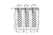
次に、図18A〜図18Cに示すように、第4の絶縁膜13が除去された素子分離溝(第1の溝)4内を埋め込むことにより、露出させていた上部側面1cbに接触する第1の半導体膜22を形成し、その第1の半導体膜22に不純物を注入してビット線コンタクト22aを形成する。
図18Aに示すように、図16で示した段階で第4の絶縁膜13が除去されなかった素子分離溝4には第4の絶縁膜13が埋め込まれているので、その素子分離溝4内には第1の半導体膜22は埋め込まれない。すなわち、y方向(第1の方向)には所定数ごとに、ビット線コンタクト22aに接続する不純物拡散領域23aを上方に有する半導体ピラー1dが配置するため、y方向(第1の方向)に所定数ごとに、ビット線コンタクト22aを形成するために第4の絶縁膜13が除去された素子分離溝4が配置し、それ以外のビット線コンタクト22aが形成されない素子分離溝4については第4の絶縁膜13は除去されずに残ったままである。(Bit line contact formation process)
Next, as shown in FIGS. 18A to 18C, the element isolation trench (first trench) 4 from which the fourth insulating
As shown in FIG. 18A, since the fourth insulating
具体的には例えば、素子分離溝(第1の溝)4内及びマスク用シリコン窒化膜(第1の絶縁膜)2の全面に覆うように、CVD法によって、リン等のn型ドーパントを22×1019/cm3の濃度でドープしたシリコン膜(第1の半導体膜)22を成膜した後、マスク用シリコン窒化膜(第1の絶縁膜)2が露出するまでエッチバックして、素子分離溝4内を埋め込むビット線コンタクト22aを形成する。
この工程により、y方向(第1の方向)にはビット線コンタクト22a、シリコン酸化膜(第4の絶縁膜)13、シリコン酸化膜(第4の絶縁膜)13、ビット線コンタクト22a・・・のように、3個目ごとにビット線コンタクト22aが配置する。Specifically, for example, an n-type dopant such as phosphorus is 22 by CVD so as to cover the entire surface of the element isolation groove (first groove) 4 and the mask silicon nitride film (first insulating film) 2. A silicon film (first semiconductor film) 22 doped at a concentration of × 1019 / cm3 is formed, and then etched back until the mask silicon nitride film (first insulating film) 2 is exposed. A
By this step, in the y direction (first direction), the
(拡散領域の形成工程)
次に、図19A〜図19Cに示すように、上記のビット線コンタクトの形成工程においてビット線コンタクト22aにドープされた不純物を、半導体ピラー1dの上部側面1cbを介して半導体ピラー1dの上部に拡散させて不純物拡散領域23(23a)を形成する。(Diffusion region formation process)
Next, as shown in FIGS. 19A to 19C, the impurity doped in the
具体的には例えば、ビット線コンタクト22aにドープされた不純物を、熱拡散によって、半導体ピラー1dの上部側面1cbを介して半導体ピラー1dの上部に拡散させて不純物拡散領域23(23a)を形成する。
この工程により、ビット線コンタクト22aに電気的に接続する不純物拡散領域23aが3個目ごとの半導体ピラー1dの上部に形成される。Specifically, for example, the impurity doped in the
By this step, an
(ビット線の形成工程)
次に、図19A〜図19Cに示すように、ビット線コンタクト22a上にy方向(第1の方向)に延在するビット線26を形成する。(Bit line formation process)
Next, as shown in FIGS. 19A to 19C, the
具体的には例えば、マスク用シリコン窒化膜(第1の絶縁膜)2、ビット線コンタクト22a及びサイドウォール(第3の絶縁膜)7aの全面に、不純物をドープしたポリシリコン層24を成膜する。なお、不純物をドープしたポリシリコン層24は、CVD法による成膜段階で不純物を含有させることができる。また、ノンドープシリコン膜を形成した後に、イオン注入により不純物を含有させることもできる。次に、この不純物ドープポリシリコン層上に、窒化タングステン(WN)膜とタングステン(W)膜とを順次堆積させることによりメタル膜25を形成する。窒化タングステンを形成する前にポリシリコン層24の表面にメタルシリサイド膜を形成することができる。メタルシリサイド膜にはチタンシリサイド、タングステンシリサイド、コバルトシリサイド、ニッケルシリサイドなどを用いることができる。これにより、より低抵抗なビット線を形成することができる。
次に、従来公知のリソグラフィ及びドライエッチング技術を用いて、W/WN膜およびポリシリコン層からなる積層膜をライン形状にパターニングすることにより、図19A及び図19Cに示すようなメタル膜25及びポリシリコン層24からなるビット線26を形成することができる。ビット線26の形成においては、素子分離溝(第1の溝)4の中央に、ビット線26の中心が位置するようにリソグラフィ段階での位置合わせを調整する。さらに、加工のマスクとなる図示しないホトレジストに公知の細線化処理を施して細線かし、素子分離溝の幅よりビット線26の幅を狭くする。これにより、次の工程で形成されるサイドウォール絶縁膜27の側壁端部が隣接するストレージノードコンタクト30が形成される活性領域側へはみ出すことを防止することができる。
次に、LP−CVD法を用いて、全面にビット線26を覆うようにシリコン窒化膜を成膜し、ビット線26の側面にのみシリコン窒化膜が残るようにパターニングしてシリコン窒化膜からなるサイドウォール絶縁膜27を形成する。
この工程により、ビット線コンタクト22aに電気的に接続するメタル膜25及びポリシリコン層24からなるビット線26が形成される。
本実施例では、上記のようにポリシリコン層24とメタル層25の積層膜でビット線26を形成しているが、ポリシリコン層24の形成を省略してメタル層25単層でビット線を構成することもできる。この構成により、ビット線の高さを低減できるので、次工程のストレージノードコンタクトの形成加工を容易化できる。Specifically, for example, a
Next, by using a conventionally known lithography and dry etching technique, the laminated film composed of the W / WN film and the polysilicon layer is patterned into a line shape, whereby the
Next, an LP-CVD method is used to form a silicon nitride film so as to cover the
By this step, the
In this embodiment, the
(ストレージノードコンタクト用ホールの形成工程)
次に、図20A〜図20Cに示すように、半導体ピラー1dのうち、ビット線コンタクト22aが接触していない半導体ピラー上の第1の絶縁膜2を除去してその半導体ピラーの上面1daを露出させ、その上面1daにストレージノードコンタクト用ホール28を形成する。
なお、図20A〜図20Cにおいて、点線で囲んだ範囲に半導体ピラー1d上にストレージノードコンタクトが形成され、さらにその上にキャパシタが形成される。(Storage node contact hole formation process)
Next, as shown in FIGS. 20A to 20C, the first insulating
20A to 20C, a storage node contact is formed on the
具体的には例えば、全面に絶縁膜29を形成した後、従来公知のリソグラフィ技術及びドライエッチング技術を用いて、絶縁膜29にストレージノードコンタクトパターンを形成してこれをマスクとし、通常の異方性ドライエッチングによって第1の絶縁膜2をエッチングすることにより、ストレージノードコンタクト用ホール28を形成する。
この工程により、ストレージノードコンタクトを形成するためのストレージノードコンタクト用ホール28を有するマスクが形成される。Specifically, for example, after an insulating
By this step, a mask having storage node contact holes 28 for forming storage node contacts is formed.
(不純物拡散領域の形成工程)
次に、図1A〜図1Cに示すように、絶縁膜29からなるストレージノードコンタクトパターンをマスクとして、露出させた半導体ピラーの上面1daから不純物を注入してその半導体ピラー1dの上部に不純物拡散領域23bを形成する。(Process for forming impurity diffusion region)
Next, as shown in FIGS. 1A to 1C, impurities are implanted from the exposed upper surface 1da of the semiconductor pillar using the storage node contact pattern made of the insulating
具体的には例えば、リン等のn型ドーパントを加速エネルギー10keV、ドーズ量1×10¹⁴/cm2の条件でイオン注入を行う。
この工程により、上方にストレージノードコンタクトが形成される半導体ピラー1dの上部に不純物拡散領域23bが形成される。Specifically, for example, ion implantation is performed on an n-type dopant such as phosphorus under conditions of an acceleration energy of 10 keV and a dose of 1 × 10¹⁴ / cm2 .
By this step, an
(ストレージノードコンタクトの形成工程)
次に、図1A〜図1Cに示すように、ストレージノードコンタクト用ホール28内に導電層を充填してビット線コンタクトが接触していない半導体ピラー上にストレージノードコンタクト30を形成する。(Storage node contact formation process)
Next, as shown in FIGS. 1A to 1C, the
具体的には例えば、絶縁膜29上に、ストレージノードコンタクト用ホール28内を埋め込むように、LP−CVD法を用いて、リンを22×1019/cm3の濃度でドープしたシリコン膜を厚さ100nm程度で堆積させる。次いで、CMP法によってポリシリコンを研磨除去することにより、ストレージノードコンタクト用ホール28内を充填するように、ストレージノードコンタクト30を形成する。
この工程により、不純物拡散領域23bを有する半導体ピラー1d上にストレージノードコンタクト30が形成される。Specifically, for example, a silicon film doped with phosphorus at a concentration of 22 × 1019 / cm3 is formed on the insulating
By this step, the
(キャパシタの形成工程)
次に、ストレージノードコンタクト30上に、コンタクトパッド(図示せず)を形成し、接続する下部電極を形成し、次いで、容量絶縁膜、上部電極を形成してキャパシタ40を形成する。
この工程により、不純物拡散領域23bを有する半導体ピラー1d上にストレージノードコンタクト30を介してキャパシタ40が形成される。(Capacitor formation process)
Next, a contact pad (not shown) is formed on the
Through this step, the
1 半導体基板
1a 素子形成領域
1c、1ca、1cb 上部側面
1d 半導体ピラー
4 素子分離溝(第1の溝)
6 素子分離領域(第2の絶縁層)
7、7a、7b 第3の絶縁膜
8 第8の絶縁膜
9 凹部
13 第4の絶縁膜
14 第2の溝
17 ワード線
21 第7の絶縁膜
21a 開口
22 第1の半導体膜
22a ビット線コンタクト
23、23a、23b 不純物拡散領域
26 ビット線
30 ストレージノードコンタクト
40 キャパシタ
100 半導体装置DESCRIPTION OF
6 Element isolation region (second insulating layer)
7, 7a, 7b
Claims (16)
Translated fromJapanese前記第1の溝の下部を埋めこんで形成された第2の絶縁層からなる素子分離領域と、
前記半導体基板の主面に形成された第1の方向に直交する第2の方向に直線状に延在する複数の第2の溝と、
前記第2の溝の下部を埋め込んで、該第2の溝の内壁上の第5の絶縁膜を介して第2の溝内に形成されたワード線と、
前記第1の溝と前記第2の溝とによって前記半導体基板内に区画して形成され、前記半導体基板の主面に対して垂直方向に立設すると共に、上部に活性領域たる不純物拡散領域を有する複数の半導体ピラーと、
第1の方向に並ぶ所定数ごとの半導体ピラーの前記上部の側面を介して前記不純物拡散領域に電気的に接続すると共に、前記第2の絶縁層上に形成されたビット線コンタクトと、
第1の方向に直線状に延在し、前記ビット線コンタクトに電気的に接続するビット線と、を備えることを特徴とする半導体装置。A plurality of first grooves formed linearly in a first direction formed in the main surface of the semiconductor substrate;
An element isolation region comprising a second insulating layer formed by embedding a lower portion of the first groove;
A plurality of second grooves extending linearly in a second direction orthogonal to the first direction formed on the main surface of the semiconductor substrate;
A word line embedded in a lower portion of the second groove and formed in the second groove via a fifth insulating film on an inner wall of the second groove;
The first groove and the second groove are partitioned and formed in the semiconductor substrate. The first groove and the second groove are erected in a direction perpendicular to the main surface of the semiconductor substrate, and an impurity diffusion region as an active region is formed on the upper portion. A plurality of semiconductor pillars having,
A bit line contact formed on the second insulating layer and electrically connected to the impurity diffusion region via the upper side surface of the predetermined number of semiconductor pillars arranged in the first direction;
And a bit line extending linearly in a first direction and electrically connected to the bit line contact.
前記ストレージノードコンタクトに電気的に接続するキャパシタと、を備えることを特徴とする請求項1から8のいずれか一項に記載の半導体装置。A storage node contact electrically connected to the impurity diffusion region through the upper surface of the semiconductor pillar other than the predetermined number of semiconductor pillars;
The semiconductor device according to claim 1, further comprising a capacitor electrically connected to the storage node contact.
前記第1の溝に、前記素子形成領域の上部側面が露出されたままとするように、第1の溝の下部を埋めこんで第2の絶縁膜を形成する工程と、
前記素子形成領域の、第1の方向に平行な一対の上部側面のうち一方の上部側面上にのみ、前記第1の溝の下部を埋めこんで第3の絶縁膜を形成する工程と、
前記第1の溝を埋め込むように、前記第3の絶縁膜と異なる材料からなる第4の絶縁膜を形成する工程と、
前記半導体基板の面内に第1の方向に直交する第2の方向に直線状に延在する複数の第2の溝を形成すると共に、これによって前記素子形成領域を第2の方向で分離して複数の半導体ピラーを形成する工程と、
前記第2の溝内の下部に該第2の溝の内壁に形成した第5の絶縁膜を介してワード線を形成すると共に、前記第2の溝内の前記ワード線上に第6の絶縁膜を形成する工程と、
第1の方向において所定数の半導体ピラーごとに、第2の方向に並ぶ複数の半導体ピラーの上方に第2の方向に延在する開口を有する第7の絶縁膜を全面に形成する工程と、
前記第7の絶縁膜をマスクとして前記第3の絶縁膜よりも前記第4の絶縁膜に対してエッチング速度が高い溶液で湿式エッチングを施して、前記第4の絶縁膜のうち前記開口の形成により露出された第4の絶縁膜を一括して除去して、前記一対の上部側面のうち前記第3の絶縁膜が形成されていない方の上部側面を露出させる工程と、
前記第7の絶縁膜を除去する工程と、
前記第4の絶縁膜が除去された前記第1の溝内を埋め込むことにより前記露出させた上部側面に接触する、不純物がドープされた第1の半導体膜からなるビット線コンタクトを形成する工程と、
前記不純物を前記接触する上部側面を介して前記半導体ピラーの上部に拡散させて拡散領域を形成する工程と、
前記ビット線コンタクト上に第1の方向に延在するビット線を形成する工程と、
前記半導体ピラーのうち、前記ビット線コンタクトが接触していない半導体ピラー上の前記第1の絶縁膜を除去してその半導体ピラーの上面を露出させ、その上面にストレージノードコンタクトを形成する工程と、を備えることを特徴とする半導体装置の製造方法。In the surface of the semiconductor substrate, a plurality of first grooves extending linearly in the first direction are formed using a first insulating film, and thereby an element formation region between adjacent first grooves Forming a step;
Forming a second insulating film by embedding a lower portion of the first groove so that an upper side surface of the element formation region remains exposed in the first groove;
Forming a third insulating film by embedding a lower portion of the first groove only on one upper side surface of a pair of upper side surfaces parallel to the first direction in the element formation region;
Forming a fourth insulating film made of a material different from that of the third insulating film so as to fill the first trench;
A plurality of second grooves extending linearly in a second direction orthogonal to the first direction are formed in the surface of the semiconductor substrate, thereby separating the element formation region in the second direction. Forming a plurality of semiconductor pillars;
A word line is formed in the lower part of the second groove via a fifth insulating film formed on the inner wall of the second groove, and a sixth insulating film is formed on the word line in the second groove. Forming a step;
Forming a seventh insulating film having an opening extending in the second direction above the plurality of semiconductor pillars arranged in the second direction for every predetermined number of semiconductor pillars in the first direction;
Using the seventh insulating film as a mask, wet etching is performed with a solution having a higher etching rate than the third insulating film with respect to the fourth insulating film to form the opening in the fourth insulating film. Removing the fourth insulating film exposed at once to expose the upper side surface of the pair of upper side surfaces on which the third insulating film is not formed;
Removing the seventh insulating film;
Forming a bit line contact made of an impurity-doped first semiconductor film that contacts the exposed upper side surface by embedding the first trench from which the fourth insulating film has been removed; ,
Diffusing the impurities into the upper portion of the semiconductor pillar through the contacting upper side surface to form a diffusion region;
Forming a bit line extending in a first direction on the bit line contact;
Removing the first insulating film on the semiconductor pillar that is not in contact with the bit line contact among the semiconductor pillars, exposing an upper surface of the semiconductor pillar, and forming a storage node contact on the upper surface; A method for manufacturing a semiconductor device, comprising:
前記素子形成領域の前記一対の上部側面のそれぞれに、前記第1の溝の下部を埋めこんで前記第3の絶縁膜を形成する小工程と、
前記第1の溝4内に前記第3の絶縁膜と異なる材料からなる第8の絶縁膜を、前記第3の絶縁膜の上面より低くなるように形成して、前記第1の溝内の前記第8の絶縁膜上に凹部を形成する小工程と、
前記凹部の下部を埋めこんで、該凹部を含む全面に第2の半導体膜を形成する小工程と、
前記第2の半導体膜にその垂直方向に対して傾いた角度から不純物を注入した後、湿式エッチングを施して、前記第2の半導体膜のうち、前記一方の上部側面と反対側の上部側面上の第3の絶縁膜を介して形成されている第2の半導体膜の部分と、前記第8の絶縁膜上の第2の半導体膜の部分の一部とを除去する小工程と、
前記一対の上部側面のうち前記一方の上部側面と反対側の上部側面上の第3の絶縁膜を除去する小工程と、
前記第8の絶縁膜を除去する小工程と、
前記第2の半導体膜を除去する小工程と、を有することを特徴とする請求項10に記載の半導体装置の製造方法。The step of forming the third insulating film only on the one upper side surface is as follows:
A small step of forming the third insulating film by embedding a lower portion of the first groove in each of the pair of upper side surfaces of the element formation region;
An eighth insulating film made of a material different from that of the third insulating film is formed in the first groove 4 so as to be lower than the upper surface of the third insulating film. A small step of forming a recess on the eighth insulating film;
A small process of embedding a lower portion of the recess and forming a second semiconductor film on the entire surface including the recess;
Impurities are implanted into the second semiconductor film from an angle inclined with respect to the vertical direction, and then wet etching is performed on the upper side surface of the second semiconductor film opposite to the one upper side surface. A small step of removing a portion of the second semiconductor film formed through the third insulating film and a portion of the portion of the second semiconductor film on the eighth insulating film;
A small step of removing the third insulating film on the upper side surface opposite to the one upper side surface of the pair of upper side surfaces;
A small step of removing the eighth insulating film;
The method for manufacturing a semiconductor device according to claim 10, further comprising a small step of removing the second semiconductor film.
Priority Applications (2)
| Application Number | Priority Date | Filing Date | Title |
|---|---|---|---|
| JP2011033431AJP2012174790A (en) | 2011-02-18 | 2011-02-18 | Semiconductor device and manufacturing method of the same |
| US13/398,275US8841717B2 (en) | 2011-02-18 | 2012-02-16 | Semiconductor device and method of forming the same |
Applications Claiming Priority (1)
| Application Number | Priority Date | Filing Date | Title |
|---|---|---|---|
| JP2011033431AJP2012174790A (en) | 2011-02-18 | 2011-02-18 | Semiconductor device and manufacturing method of the same |
Publications (1)
| Publication Number | Publication Date |
|---|---|
| JP2012174790Atrue JP2012174790A (en) | 2012-09-10 |
Family
ID=46652039
Family Applications (1)
| Application Number | Title | Priority Date | Filing Date |
|---|---|---|---|
| JP2011033431ACeasedJP2012174790A (en) | 2011-02-18 | 2011-02-18 | Semiconductor device and manufacturing method of the same |
Country Status (2)
| Country | Link |
|---|---|
| US (1) | US8841717B2 (en) |
| JP (1) | JP2012174790A (en) |
Cited By (4)
| Publication number | Priority date | Publication date | Assignee | Title |
|---|---|---|---|---|
| KR20140072615A (en)* | 2012-12-05 | 2014-06-13 | 삼성전자주식회사 | Method for fabricating a semiconductor device |
| CN110896076A (en)* | 2018-09-13 | 2020-03-20 | 长鑫存储技术有限公司 | Semiconductor device and method of making the same |
| KR20210026193A (en)* | 2019-08-29 | 2021-03-10 | 삼성전자주식회사 | Semiconductor and manufacturing method thereof |
| JP7578483B2 (en) | 2020-12-23 | 2024-11-06 | 株式会社Screenホールディングス | Semiconductor element forming method and substrate processing apparatus |
Families Citing this family (9)
| Publication number | Priority date | Publication date | Assignee | Title |
|---|---|---|---|---|
| JP2011077185A (en)* | 2009-09-29 | 2011-04-14 | Elpida Memory Inc | Semiconductor device, method of manufacturing semiconductor device, and data processing system |
| KR20130110733A (en)* | 2012-03-30 | 2013-10-10 | 삼성전자주식회사 | Method of forming semiconductor device and the device formed by the method |
| US8710570B2 (en)* | 2012-07-24 | 2014-04-29 | SK Hynix Inc. | Semiconductor device having vertical channel |
| KR20150028521A (en)* | 2013-09-06 | 2015-03-16 | 에스케이하이닉스 주식회사 | Line Layout for Semiconductor Memory Apparatus |
| US9450059B2 (en)* | 2013-09-06 | 2016-09-20 | Kabushiki Kaisha Toshiba | Semiconductor device and method of manufacturing the same |
| JP2015195262A (en)* | 2014-03-31 | 2015-11-05 | マイクロン テクノロジー, インク. | Semiconductor device and manufacturing method of the same |
| US11978774B2 (en)* | 2020-10-05 | 2024-05-07 | Sandisk Technologies Llc | High voltage field effect transistor with vertical current paths and method of making the same |
| US12284801B2 (en)* | 2021-03-18 | 2025-04-22 | Changxin Memory Technologies, Inc. | Semiconductor structure and manufacturing method thereof |
| CN115568207A (en)* | 2021-07-02 | 2023-01-03 | 长鑫存储技术有限公司 | Semiconductor structure and preparation method of semiconductor structure |
Citations (12)
| Publication number | Priority date | Publication date | Assignee | Title |
|---|---|---|---|---|
| JPH06291277A (en)* | 1993-04-02 | 1994-10-18 | Nec Corp | Semiconductor memory device and its manufacture |
| JPH07297297A (en)* | 1994-04-22 | 1995-11-10 | Nec Corp | Semiconductor memory device and method of manufacturing |
| JPH08125144A (en)* | 1994-10-21 | 1996-05-17 | Nec Corp | Semiconductor memory and fabrication thereof |
| JPH08241966A (en)* | 1995-02-02 | 1996-09-17 | Internatl Business Mach Corp <Ibm> | Trench dram cell |
| JPH11297951A (en)* | 1998-02-13 | 1999-10-29 | Hitachi Ltd | Semiconductor integrated circuit device and method of manufacturing the same |
| JP2000208766A (en)* | 1999-01-19 | 2000-07-28 | Mitsubishi Electric Corp | Semiconductor device manufacturing method and semiconductor device |
| WO2002073696A1 (en)* | 2001-03-12 | 2002-09-19 | Hitachi, Ltd. | Process for producing semiconductor integrated circuit device |
| JP2002541666A (en)* | 1999-03-30 | 2002-12-03 | インフィネオン テクノロジース アクチエンゲゼルシャフト | Memory cell device and method of manufacturing the same |
| JP2003158201A (en)* | 2001-11-20 | 2003-05-30 | Sony Corp | Semiconductor device and its manufacturing method |
| US20080048230A1 (en)* | 2006-08-22 | 2008-02-28 | Elpida Memory, Inc. | Semiconductor device and method for manufacturing the same |
| JP2008300843A (en)* | 2007-05-30 | 2008-12-11 | Qimonda Ag | Transistor, integrated circuit, and integrated circuit forming method |
| JP2010141107A (en)* | 2008-12-11 | 2010-06-24 | Elpida Memory Inc | Semiconductor device and method of manufacturing the same |
Family Cites Families (5)
| Publication number | Priority date | Publication date | Assignee | Title |
|---|---|---|---|---|
| JP2000307084A (en) | 1999-04-23 | 2000-11-02 | Hitachi Ltd | Semiconductor integrated circuit device and method of manufacturing the same |
| TW201007930A (en)* | 2008-08-07 | 2010-02-16 | Nanya Technology Corp | Dynamic random access memory structure, array thereof, and method of making the same |
| JP5679628B2 (en) | 2008-12-16 | 2015-03-04 | ピーエスフォー ルクスコ エスエイアールエルPS4 Luxco S.a.r.l. | Semiconductor device and manufacturing method thereof |
| KR101561061B1 (en)* | 2009-04-10 | 2015-10-16 | 삼성전자주식회사 | Semiconductor device having a protrusion typed isolation layer |
| KR101194916B1 (en)* | 2010-04-09 | 2012-10-25 | 에스케이하이닉스 주식회사 | Semiconductor device and method of manufacturing the same |
- 2011
- 2011-02-18JPJP2011033431Apatent/JP2012174790A/ennot_activeCeased
- 2012
- 2012-02-16USUS13/398,275patent/US8841717B2/ennot_activeExpired - Fee Related
Patent Citations (13)
| Publication number | Priority date | Publication date | Assignee | Title |
|---|---|---|---|---|
| JPH06291277A (en)* | 1993-04-02 | 1994-10-18 | Nec Corp | Semiconductor memory device and its manufacture |
| JPH07297297A (en)* | 1994-04-22 | 1995-11-10 | Nec Corp | Semiconductor memory device and method of manufacturing |
| JPH08125144A (en)* | 1994-10-21 | 1996-05-17 | Nec Corp | Semiconductor memory and fabrication thereof |
| JPH08241966A (en)* | 1995-02-02 | 1996-09-17 | Internatl Business Mach Corp <Ibm> | Trench dram cell |
| JPH11297951A (en)* | 1998-02-13 | 1999-10-29 | Hitachi Ltd | Semiconductor integrated circuit device and method of manufacturing the same |
| JP2000208766A (en)* | 1999-01-19 | 2000-07-28 | Mitsubishi Electric Corp | Semiconductor device manufacturing method and semiconductor device |
| JP2002541666A (en)* | 1999-03-30 | 2002-12-03 | インフィネオン テクノロジース アクチエンゲゼルシャフト | Memory cell device and method of manufacturing the same |
| WO2002073696A1 (en)* | 2001-03-12 | 2002-09-19 | Hitachi, Ltd. | Process for producing semiconductor integrated circuit device |
| JP2003158201A (en)* | 2001-11-20 | 2003-05-30 | Sony Corp | Semiconductor device and its manufacturing method |
| US20080048230A1 (en)* | 2006-08-22 | 2008-02-28 | Elpida Memory, Inc. | Semiconductor device and method for manufacturing the same |
| JP2008053274A (en)* | 2006-08-22 | 2008-03-06 | Elpida Memory Inc | Semiconductor device and manufacturing method thereof |
| JP2008300843A (en)* | 2007-05-30 | 2008-12-11 | Qimonda Ag | Transistor, integrated circuit, and integrated circuit forming method |
| JP2010141107A (en)* | 2008-12-11 | 2010-06-24 | Elpida Memory Inc | Semiconductor device and method of manufacturing the same |
Cited By (6)
| Publication number | Priority date | Publication date | Assignee | Title |
|---|---|---|---|---|
| KR20140072615A (en)* | 2012-12-05 | 2014-06-13 | 삼성전자주식회사 | Method for fabricating a semiconductor device |
| KR101979901B1 (en) | 2012-12-05 | 2019-08-28 | 삼성전자주식회사 | Method for fabricating a semiconductor device |
| CN110896076A (en)* | 2018-09-13 | 2020-03-20 | 长鑫存储技术有限公司 | Semiconductor device and method of making the same |
| KR20210026193A (en)* | 2019-08-29 | 2021-03-10 | 삼성전자주식회사 | Semiconductor and manufacturing method thereof |
| KR102784723B1 (en)* | 2019-08-29 | 2025-03-21 | 삼성전자주식회사 | Semiconductor and manufacturing method thereof |
| JP7578483B2 (en) | 2020-12-23 | 2024-11-06 | 株式会社Screenホールディングス | Semiconductor element forming method and substrate processing apparatus |
Also Published As
| Publication number | Publication date |
|---|---|
| US20120211815A1 (en) | 2012-08-23 |
| US8841717B2 (en) | 2014-09-23 |
Similar Documents
| Publication | Publication Date | Title |
|---|---|---|
| JP2012174790A (en) | Semiconductor device and manufacturing method of the same | |
| KR100675285B1 (en) | Semiconductor device having vertical transistor and manufacturing method thereof | |
| US8716774B2 (en) | Semiconductor device having a buried gate type MOS transistor and method of manufacturing same | |
| US9245893B1 (en) | Semiconductor constructions having grooves dividing active regions | |
| US7847322B2 (en) | Semiconductor memory device and method of manufacturing the same | |
| KR20130103908A (en) | Semiconductor device with buried bit line and method for fabricating the same | |
| US8928073B2 (en) | Semiconductor devices including guard ring structures | |
| JP2012174866A (en) | Semiconductor device and manufacturing method of the same | |
| KR20110099502A (en) | Semiconductor device and manufacturing method thereof | |
| JP3927179B2 (en) | Semiconductor memory device and manufacturing method thereof | |
| JP2011187652A (en) | Semiconductor device and method of manufacturing the same | |
| CN102867752A (en) | Method for fabricating semiconductor device with vertical gate | |
| JP2013168569A (en) | Semiconductor device and manufacturing method of the same | |
| US20160027785A1 (en) | Semiconductor device and method for manufacturing same | |
| WO2014123170A1 (en) | Semiconductor device and method for manufacturing same | |
| JP2011243802A (en) | Semiconductor device, manufacturing method thereof, and data processing system | |
| US20160086956A1 (en) | Semiconductor device and method for manufacturing semiconductor device | |
| JP2005123243A (en) | Semiconductor device and manufacturing method thereof | |
| US8741755B2 (en) | Semiconductor device having gate trench and manufacturing method thereof | |
| JP2010050133A (en) | Semiconductor device, and method of manufacturing the same | |
| US20100155891A1 (en) | Semiconductor device having cylindrical lower electrode of capacitor and manufacturing method thereof | |
| JP2009182114A (en) | Semiconductor device and manufacturing method thereof | |
| US8999827B2 (en) | Semiconductor device manufacturing method | |
| JP2008053274A (en) | Semiconductor device and manufacturing method thereof | |
| US8785274B2 (en) | Method for manufacturing semiconductor device |
Legal Events
| Date | Code | Title | Description |
|---|---|---|---|
| A711 | Notification of change in applicant | Free format text:JAPANESE INTERMEDIATE CODE: A711 Effective date:20130731 | |
| A521 | Request for written amendment filed | Free format text:JAPANESE INTERMEDIATE CODE: A821 Effective date:20130801 | |
| A521 | Request for written amendment filed | Free format text:JAPANESE INTERMEDIATE CODE: A523 Effective date:20130905 | |
| RD02 | Notification of acceptance of power of attorney | Free format text:JAPANESE INTERMEDIATE CODE: A7422 Effective date:20131108 | |
| RD04 | Notification of resignation of power of attorney | Free format text:JAPANESE INTERMEDIATE CODE: A7424 Effective date:20131219 | |
| A621 | Written request for application examination | Free format text:JAPANESE INTERMEDIATE CODE: A621 Effective date:20140205 | |
| A977 | Report on retrieval | Free format text:JAPANESE INTERMEDIATE CODE: A971007 Effective date:20141128 | |
| A131 | Notification of reasons for refusal | Free format text:JAPANESE INTERMEDIATE CODE: A131 Effective date:20141202 | |
| A601 | Written request for extension of time | Free format text:JAPANESE INTERMEDIATE CODE: A601 Effective date:20150302 | |
| RD03 | Notification of appointment of power of attorney | Free format text:JAPANESE INTERMEDIATE CODE: A7423 Effective date:20150327 | |
| A521 | Request for written amendment filed | Free format text:JAPANESE INTERMEDIATE CODE: A523 Effective date:20150331 | |
| RD04 | Notification of resignation of power of attorney | Free format text:JAPANESE INTERMEDIATE CODE: A7424 Effective date:20150501 | |
| A131 | Notification of reasons for refusal | Free format text:JAPANESE INTERMEDIATE CODE: A131 Effective date:20150512 | |
| A601 | Written request for extension of time | Free format text:JAPANESE INTERMEDIATE CODE: A601 Effective date:20150803 | |
| A521 | Request for written amendment filed | Free format text:JAPANESE INTERMEDIATE CODE: A523 Effective date:20151110 | |
| A01 | Written decision to grant a patent or to grant a registration (utility model) | Free format text:JAPANESE INTERMEDIATE CODE: A01 Effective date:20160322 | |
| A045 | Written measure of dismissal of application [lapsed due to lack of payment] | Free format text:JAPANESE INTERMEDIATE CODE: A045 Effective date:20160726 |