JP2012174723A - Thin film transistor, manufacturing method thereof, and display device - Google Patents
Thin film transistor, manufacturing method thereof, and display deviceDownload PDFInfo
- Publication number
- JP2012174723A JP2012174723AJP2011032207AJP2011032207AJP2012174723AJP 2012174723 AJP2012174723 AJP 2012174723AJP 2011032207 AJP2011032207 AJP 2011032207AJP 2011032207 AJP2011032207 AJP 2011032207AJP 2012174723 AJP2012174723 AJP 2012174723A
- Authority
- JP
- Japan
- Prior art keywords
- film
- oxide semiconductor
- channel
- channel layer
- thin film
- Prior art date
- Legal status (The legal status is an assumption and is not a legal conclusion. Google has not performed a legal analysis and makes no representation as to the accuracy of the status listed.)
- Granted
Links
Images


Classifications
- H—ELECTRICITY
- H10—SEMICONDUCTOR DEVICES; ELECTRIC SOLID-STATE DEVICES NOT OTHERWISE PROVIDED FOR
- H10D—INORGANIC ELECTRIC SEMICONDUCTOR DEVICES
- H10D30/00—Field-effect transistors [FET]
- H10D30/60—Insulated-gate field-effect transistors [IGFET]
- H10D30/67—Thin-film transistors [TFT]
- H10D30/674—Thin-film transistors [TFT] characterised by the active materials
- H10D30/6755—Oxide semiconductors, e.g. zinc oxide, copper aluminium oxide or cadmium stannate
- H—ELECTRICITY
- H10—SEMICONDUCTOR DEVICES; ELECTRIC SOLID-STATE DEVICES NOT OTHERWISE PROVIDED FOR
- H10D—INORGANIC ELECTRIC SEMICONDUCTOR DEVICES
- H10D30/00—Field-effect transistors [FET]
- H10D30/60—Insulated-gate field-effect transistors [IGFET]
- H10D30/67—Thin-film transistors [TFT]
- H10D30/6704—Thin-film transistors [TFT] having supplementary regions or layers in the thin films or in the insulated bulk substrates for controlling properties of the device
- H—ELECTRICITY
- H10—SEMICONDUCTOR DEVICES; ELECTRIC SOLID-STATE DEVICES NOT OTHERWISE PROVIDED FOR
- H10D—INORGANIC ELECTRIC SEMICONDUCTOR DEVICES
- H10D99/00—Subject matter not provided for in other groups of this subclass
Landscapes
- Thin Film Transistor (AREA)
Abstract
Description
Translated fromJapanese本発明は、酸化物半導体を用いた薄膜トランジスタ(TFT;Thin Film Transistor)およびその製造方法、並びにこの薄膜トランジスタを備えた表示装置に関する。 The present invention relates to a thin film transistor (TFT) using an oxide semiconductor, a manufacturing method thereof, and a display device including the thin film transistor.
亜鉛(Zn),インジウム(In),ガリウム(Ga),スズ(Sn),アルミニウム(Al)またはチタン(Ti)の酸化物あるいはこれらの混合物の酸化物で構成された酸化物半導体は、優れた半導体特性を示すことが知られている。そのため近年ではアクティブマトリクス型ディスプレイの駆動素子として、TFTへの応用が盛んに研究されている。このような酸化物半導体をTFTに用いた場合、液晶ディスプレイなどに一般的に使用される非晶質(アモルファス)シリコンを用いたTFTと比較して、電子移動度は10倍以上となり、更に、良好なオフ特性をも示すことがわかっている。また、室温付近程度の低温でも高い移動度が期待でき、酸化物半導体を用いたTFTは、大画面、高精細および高フレームレートの液晶ディスプレイ、有機EL(Electro Luminescence)ディスプレイ向けの応用が渇望されている。 An oxide semiconductor composed of an oxide of zinc (Zn), indium (In), gallium (Ga), tin (Sn), aluminum (Al) or titanium (Ti) or a mixture thereof is excellent. It is known to exhibit semiconductor properties. Therefore, in recent years, application to TFT has been actively studied as a driving element for an active matrix display. When such an oxide semiconductor is used for a TFT, the electron mobility is 10 times or more compared to a TFT using amorphous silicon generally used for a liquid crystal display or the like. It has been found that it also exhibits good off characteristics. In addition, high mobility can be expected even at low temperatures around room temperature, and TFTs using oxide semiconductors are eagerly desired for applications in large-screen, high-definition and high-frame-rate liquid crystal displays and organic EL (Electro Luminescence) displays. ing.
酸化物半導体を用いたTFTでは、ボトムゲート型およびトップゲート型の構造を有するTFTがこれまでに報告されている(例えば、特許文献1,特許文献2,非特許文献1および非特許文献2)。ボトムゲート型の構造の一例としては、基板側より順にゲート電極およびゲート絶縁膜を設け、その上面を被覆するように酸化物半導体の薄膜層を形成した構造が知られている。この構造は、現在事業化されている非晶質シリコンをチャネルとして用いたボトムゲート型のTFT構造と類似している。このため、既存の非晶質シリコンによるTFTの製造プロセスを転用し易く、酸化物半導体を利用したTFTにおいても、ボトムゲート型の構造が多く用いられている。 Regarding TFTs using oxide semiconductors, TFTs having bottom-gate and top-gate structures have been reported so far (for example, Patent Document 1, Patent Document 2, Non-Patent Document 1, and Non-Patent Document 2). . As an example of a bottom-gate structure, a structure in which a gate electrode and a gate insulating film are provided in this order from the substrate side, and a thin film layer of an oxide semiconductor is formed so as to cover the upper surface thereof is known. This structure is similar to a bottom-gate TFT structure using amorphous silicon as a channel, which is currently commercialized. For this reason, it is easy to divert the manufacturing process of the existing amorphous silicon TFT, and the bottom gate type structure is often used also in the TFT using the oxide semiconductor.
しかしながら、このような酸化物半導体を用いたTFTでは、チャネルとしての機能を有する酸化物半導体を島状に成形する際にフォトレジストが付着することにより、TFT特性の劣化が生じる虞がある。 However, in a TFT using such an oxide semiconductor, there is a possibility that TFT characteristics may be deteriorated due to adhesion of a photoresist when an oxide semiconductor having a channel function is formed into an island shape.
本発明はかかる問題点に鑑みてなされたもので、その目的は、酸化物半導体をチャネル層に用い、良好なTFT特性を得ることの可能な薄膜トランジスタおよびその製造方法、並びにこの薄膜トランジスタを備えた表示装置を提供することにある。 The present invention has been made in view of such problems, and an object of the present invention is to provide a thin film transistor capable of obtaining good TFT characteristics using an oxide semiconductor for a channel layer, a manufacturing method thereof, and a display including the thin film transistor. To provide an apparatus.
本発明による第1の薄膜トランジスタの製造方法は、ゲート電極上にゲート絶縁膜を間にして酸化物半導体からなるチャネル層およびチャネル層を覆うと共に導電性材料から
なるチャネル保護膜を形成した後、チャネル保護膜に接するよう一対のソース・ドレイン電極を形成する工程と、チャネル保護膜のソース・ドレイン電極間の領域を導電性材料と結晶酸化物半導体との選択性を利用したエッチングにより除去する工程とを含むものである。In the first thin film transistor manufacturing method according to the present invention, a channel layer made of an oxide semiconductor and a channel protective film made of a conductive material are formed on a gate electrode with a gate insulating film therebetween, and then a channel protective film is formed. Forming a pair of source / drain electrodes so as to be in contact with the protective film, and removing a region between the source / drain electrodes of the channel protective film by etching utilizing selectivity between a conductive material and a crystalline oxide semiconductor; Is included.
本発明による第2の薄膜トランジスタの製造方法は、酸化物半導体からなるチャネル層およびチャネル層を覆うと共に導電性材料からなるチャネル保護膜を形成する工程と、チャネル保護膜を導電性材料と結晶酸化物半導体との選択性を利用したエッチングにより除去する工程と、ゲート絶縁膜を間にして前記チャネル層上にゲート電極およびチャネル層に接する一対のソース・ドレイン電極を形成する工程とを含むものである。 The second thin film transistor manufacturing method according to the present invention includes a step of forming a channel layer made of an oxide semiconductor and a channel protective film covering the channel layer and made of a conductive material, and forming the channel protective film from a conductive material and a crystalline oxide. A step of removing by etching utilizing selectivity with a semiconductor, and a step of forming a pair of source / drain electrodes in contact with the channel layer on the channel layer with the gate insulating film therebetween.
本発明の薄膜トランジスタの製造方法では、酸化物半導体を成形して、即ち、フォトリソグラフィーおよびエッチング工程によりチャネル層を形成する際に、酸化物半導体膜が導電性膜(即ちチャネル保護膜)に覆われているため、フォトレジストによる化学物質の付着等からチャネル層(酸化物半導体膜)が保護される。更に、チャネル層が結晶酸化物半導体からなるため、チャネル保護膜をエッチングする工程において、チャネル層とチャネル保護膜との間の選択的なエッチングが容易となる。 In the thin film transistor manufacturing method of the present invention, an oxide semiconductor film is covered with a conductive film (that is, a channel protective film) when an oxide semiconductor is formed, that is, when a channel layer is formed by photolithography and etching processes. Therefore, the channel layer (oxide semiconductor film) is protected from adhesion of chemical substances by the photoresist. Further, since the channel layer is made of a crystalline oxide semiconductor, selective etching between the channel layer and the channel protective film is facilitated in the step of etching the channel protective film.
本発明による薄膜トランジスタは、ゲート電極と、ゲート電極上にゲート絶縁膜を介して設けられた、結晶酸化物半導体よりなるチャネル層と、導電性膜により構成され、チャネル層に接すると共に互いに電気的に分離された一対のチャネル保護膜と、それぞれチャネル保護膜を介してチャネル層に電気的に接続された一対のソース・ドレイン電極とを備えたものである。 The thin film transistor according to the present invention includes a gate electrode, a channel layer made of a crystalline oxide semiconductor provided on the gate electrode through a gate insulating film, and a conductive film, and is in contact with the channel layer and electrically A pair of separated channel protective films and a pair of source / drain electrodes electrically connected to the channel layer through the channel protective films, respectively.
また、本発明による表示装置は、画素トランジスタとして、上記本発明の薄膜トランジスタを備えたものであり、当該薄膜トランジスタによって画素が駆動され、画像表示がなされる。 The display device according to the present invention includes the thin film transistor of the present invention as a pixel transistor, and the pixel is driven by the thin film transistor to display an image.
本発明の薄膜トランジスタおよびその製造方法、並びにこの薄膜トランジスタを備えた表示装置によれば、酸化物半導体を成形してチャネル層を形成する際に、酸化物半導体膜が導電性膜(チャネル保護膜)に覆うようにしたため、チャネル層(酸化物半導体膜)の成形工程において当該チャネル層がフォトレジストにより化学汚染等から保護され、薄膜トランジスタの伝達特性の劣化が抑制される。よって、良好なTFT特性を有し、信頼性の向上した薄膜トランジスタを製造することが可能となる。更に、チャネル層を結晶酸化物半導体により形成するようにしたため、チャネル層とチャネル保護膜との間の選択的なエッチングを容易に行うことができる。 According to the thin film transistor of the present invention, the manufacturing method thereof, and the display device including the thin film transistor, when the oxide semiconductor is molded to form the channel layer, the oxide semiconductor film becomes a conductive film (channel protective film). Since the cover is formed, the channel layer (oxide semiconductor film) is protected from chemical contamination by a photoresist in the step of forming the channel layer (oxide semiconductor film), and deterioration of transfer characteristics of the thin film transistor is suppressed. Accordingly, a thin film transistor having favorable TFT characteristics and improved reliability can be manufactured. Further, since the channel layer is formed of a crystalline oxide semiconductor, selective etching between the channel layer and the channel protective film can be easily performed.
以下、本発明の実施の形態について、図面を参照して詳細に説明する。なお、説明は以下の順序で行う。
1.第1の実施の形態(ボトムゲート型薄膜トランジスタの例)
2.変形例(ボトムゲート型薄膜トランジスタ;チャネル保護膜がソース・ドレイン電極の一層を構成する例)
3.第2の実施の形態(トップゲート型薄膜トランジスタの例)Hereinafter, embodiments of the present invention will be described in detail with reference to the drawings. The description will be given in the following order.
1. First embodiment (example of bottom-gate thin film transistor)
2. Modified example (bottom gate type thin film transistor; example in which channel protective film forms one layer of source / drain electrode)
3. Second embodiment (example of top gate type thin film transistor)
〔第1の実施の形態〕
図1は本発明の第1の実施の形態に係るボトムゲート型(逆スタガ型)の薄膜トランジ
スタ1の断面構成を表すものである。薄膜トランジスタ1は、液晶ディスプレイや有機E
Lディスプレイなどの駆動素子として用いられるものである。この薄膜トランジスタ1は、
例えば、基板10上にゲート電極11,ゲート絶縁膜12,結晶酸化物半導体からなる
チャネル層13がこの順に積層されたものであり、チャネル層13上にはチャネル保護膜
14A,14Bが設けられている。ソース・ドレイン電極15A,15Bはそれぞれチャ
ネル保護膜14A,14Bを介してチャネル層13に接続されている。ソース・ドレイン
電極15A,15B上には基板10の全面にわたって保護膜16が形成されている。[First Embodiment]
FIG. 1 shows a cross-sectional configuration of a bottom gate type (inverted stagger type) thin film transistor 1 according to a first embodiment of the present invention. The thin film transistor 1 is a liquid crystal display or organic E
It is used as a driving element for an L display or the like. The thin film transistor 1 includes:
For example, a
基板10は、ガラス基板やプラスチックフィルムなどにより構成されている。プラスチック材料としては、例えばPET(ポリエチレンテレフタレート)、PEN(ポリエチレンナフタレート)などが挙げられる。本実施の形態の薄膜トランジスタ1では、後述のスパッタリング法において、基板10を加熱することなくチャネル層13を成膜するため、安価なプラスチックフィルムを用いることができる。 The
ゲート電極11は、薄膜トランジスタ1にゲート電圧を印加し、このゲート電圧によりチャネル層13中のキャリア密度を制御する役割を有するものである。ゲート電極11は基板10上の選択的な領域に設けられ、例えば厚みが10nm〜500nmであり、白金(Pt),チタン(Ti),ルテニウム(Ru),モリブデン(Mo),銅(Cu),タングステン(W),ニッケル(Ni),アルミニウム(Al)およびタンタル(Ta)等の金属単体または合金により構成されている。 The
ゲート絶縁膜12は、例えば、厚みが50nm〜1μmであり、シリコン酸化膜,シリコン窒化膜,シリコン酸窒化膜,ハフニウム酸化膜,アルミニウム酸化膜,タンタル酸化膜,ジルコニウム酸化膜,ハフニウム酸窒化膜,アルミニウム酸窒化膜,タンタル酸窒化膜およびジルコニウム酸窒化膜のうちの少なくとも1つを含む絶縁膜により形成される。このゲート絶縁膜12は単層構造としてもよく、または2種類以上の積層構造としてしてもよい。ゲート絶縁膜12を2種類以上の積層構造とした場合、チャネル層13との界面特性を改善したり、外気からチャネル層13への不純物の混入を抑制したりすることが可能である。 The
結晶酸化物半導体からなるチャネル層13はゲート絶縁膜12上に島状に設けられ、ソース・ドレイン電極15A,15B間のゲート電極11に対向する位置にチャネル領域13Cが形成されるようになっている。このチャネル層13は、後述のように酸化物半導体膜13A(図2(C))を成形したものであり、例えばインジウム,ガリウム,亜鉛,スズ,アルミニウムおよびチタンのうちの少なくとも1種の元素の酸化物を主成分として含んでいる。例えば、IGO(Indium-Gallium-Oxide),IZO(Indium-Zinc-Oxide),ITO(Indium-Tin-Oxide)あるいはZnO(Zinc-Oxide)等により構成され、例えば20nm〜100nm程度の膜厚を有している。 The
チャネル保護膜14A,14Bはそれぞれ、ソース・ドレイン電極15A,15Bとチャネル層13との間に配置されている。これらチャネル保護膜14A,14Bは導電性膜14(図2(C))を成形したものである。また、チャネル領域13C上のチャネル保護膜14Aとチャネル保護膜14Bとの間には間隙14Cが設けられており、両者は電気的に分離されている。即ち、ソース・ドレイン電極15A,15Bはそれぞれチャネル保護膜14A,14Bを介してチャネル層13に電気的に接続されている。 The channel
チャネル保護膜14A,14Bは例えばモリブデン,チタン,マンガン(Mn),銅またはこれらの酸化物,窒化物あるいは酸窒化物からなる導電性の材料により構成されることが望ましい。モリブデン,チタン,マンガンおよび銅は、チャネル層13と良好な密着性を示す。これにより、ソース・ドレイン電極15A,15Bと、チャネル層13との間のコンタクト抵抗を低減することができ、また、ソース・ドレイン電極15A,15Bに用いる金属材料の選択の幅を広げることが可能となる。 The channel
チャネル保護膜14A,14Bに非晶質の酸化物半導体材料を用いても、結晶酸化物半導体からなるチャネル層13とは選択的なエッチングが可能である。このようなチャネル保護膜14A,14Bは例えば同程度、すなわち20nm〜100nm程度あるいはそれ以上の厚みを有する。 Even when an amorphous oxide semiconductor material is used for the channel
ソース・ドレイン電極15A,15Bは、例えばモリブデン,アルミニウム,銅,チタン,ITO(インジウム錫酸化物)またはこれらの合金からなる金属膜の単層膜あるいは2種以上のこれらの金属膜よりなる積層膜である。例えば、モリブデン、アルミニウム、モリブデンの順に50nm、1μm、50nmの膜厚で積層した3層膜にすると、チャネル層13の電気特性を安定して保持することができる。 The source /
保護膜16は、例えば酸化アルミニウム膜,酸化窒化アルミニウム膜,シリコン酸化膜,シリコン窒化膜,酸化チタン膜または酸化窒化チタン膜などからなる薄膜により構成され、水分の吸着および酸素の透過などによるチャネル層13の電気特性の変化を抑え、薄膜トランジスタ1の電気特性を安定化する機能を有する。 The
この薄膜トランジスタ1は、例えば次のようにして製造することができる。 The thin film transistor 1 can be manufactured, for example, as follows.
図2および図3は、薄膜トランジスタ1の製造方法を工程順に表したものである。まず、基板10の全面に例えばスパッタリング法やCVD(Chemical Vapor Deposition;化学気相成長)法を用いて、ゲート電極11となる金属膜を形成する。次いで、図2(A)に示したように、基板10に形成した金属膜を、例えばフォトリソグラフィーおよびエッチング法を用いてパターニングすることにより、ゲート電極11を形成する。 2 and 3 show the method of manufacturing the thin film transistor 1 in the order of steps. First, a metal film to be the
続いて、図2(B)に示したように、基板10およびゲート電極11の全面に、例えばプラズマCVD法またはスパッタリング法により、例えばシリコン窒化膜およびシリコン酸化膜よりなるゲート絶縁膜12を形成する。 Subsequently, as shown in FIG. 2B, a
具体的には、原料ガスとしてシラン,アンモニア,窒素などのガスを用いたプラズマCVD法によりシリコン窒化膜を形成し、原料ガスとしてシラン,一酸化二窒素を含むガスなどを用いたプラズマCVD法によりシリコン酸化膜を形成する。 Specifically, a silicon nitride film is formed by a plasma CVD method using a gas such as silane, ammonia or nitrogen as a source gas, and a plasma CVD method using a gas containing silane or dinitrogen monoxide as a source gas. A silicon oxide film is formed.
ゲート絶縁膜12を形成した後、このゲート絶縁膜12上に、図2(C)に示したように、チャネル層13(図1)を構成する材料よりなる酸化物半導体膜13A、およびチャネル保護膜14A,14B(図1)を構成する材料よりなる導電性膜14を、この順に成膜する。 After the
例えば酸化物半導体膜13Aが、酸化インジウムを主として亜鉛やガリウムを含んだ半導体材料により構成される場合には次のようにして成膜を行う。即ち、酸化インジウムと酸化亜鉛や酸化ガリウムのセラミックをターゲットとしたDC(Direct Current;直流)スパッタリング法,RF(Radio Frequency;高周波)スパッタリング法またはAC(Alternating Current;交流)スパッタリング法を用いると共に、アルゴン(Ar)と酸素(O2)との混合ガスによるプラズマ放電によって、基板10およびゲート絶縁膜12上に酸化物半導体膜13Aを形成する。なお、アルゴンおよび酸素ガスの導入は、プラズマ放電前に、真空容器内を真空度が1×10⁻⁴Pa以下になるまで排気した後に行う。このとき、DC,RFまたはACのパワー,アルゴンに対する酸素濃度または水蒸気濃度およびスパッタ背圧のいずれかのうち少なくとも一つを変化させることで、酸化物半導体材料中の金属元素の組成比率や結晶性を制御することが可能となる。For example, when the
次いで、例えばモリブデンからなる導電性膜14をスパッタリング法により形成する。このように導電性膜14は、酸化物半導体膜13Aと同様の方法により容易に形成することができる。 Next, a
次いで、導電性膜14および酸化物半導体膜13Aを、例えばフォトリソグラフィーおよびエッチングの工程を経て、図3(A)に示したようにゲート電極11およびその近傍に対向する領域を含むよう島状に成形する。結晶酸化物半導体により酸化物半導体膜13Aを成膜した場合は、これによりチャネル保護膜14Dに覆われたチャネル層13が形成される。本実施の形態では、導電性膜14および酸化物半導体膜13Aを同時に成形するため、チャネル層13およびチャネル保護膜14Dは、厚み以外が同一形状、つまり同一位置に端部が形成される。このとき導電性膜14(チャネル保護膜14D)に覆われているため、酸化物半導体膜13A(チャネル層13)はフォトレジストによる化学物質の付着等から保護される。 Next, the
図2(C)に示した結晶状態の酸化物半導体膜13Aに代えて、図4(A)に示したように非晶質状態の酸化物半導体膜13Bを成膜してもよい。非晶質状態の酸化物半導体膜13Bは結晶状態の酸化物半導体13Aと比較すると、エッチング耐性が低いため、導電性膜14および酸化物半導体膜13Bを成形する際(図4(B))のエッチング方法の選択が容易となる。導電性膜14および酸化物半導体膜13Bを成形して、チャネル保護膜14Dおよび酸化物半導体膜13Cとした後、例えば、レーザ光Lの照射,ヒーター等による加熱あるいは雰囲気ガスによる加熱等の熱処理により非晶質状態の酸化物半導体から結晶状態の酸化物半導体への変換、即ち相転移を行う(図4(C))。非晶質酸化物半導体から結晶酸化物半導体への変換は、後述の金属膜15Cの成膜(図3(B))前に行うことが好ましい。相転移させるための熱処理による金属膜15Cの劣化を防ぐことができるためである。非晶質酸化物半導体から結晶酸化物半導体への相転移によりチャネル層13が形成される(図3(A))。一方、結晶状態の酸化物半導体膜13Aを成膜した場合は、このような相転移の工程が不要であり、工程数の削減を図ることができる。 Instead of the crystalline
続いて、図3(B)に示したように、例えばスパッタリング法により厚み50nm程度のチタン層、厚み1μm程度のアルミニウム層または銅層および厚み50nm程度のチタン層を順に形成し、3層の積層構造の金属膜15Cを成膜する。チタンは、酸化物半導体材料との間にチタン酸化物(TiOX)層が生成するため、酸化物半導体材料からなるチャネル層に接して形成することが困難であり、アルミニウムや銅についてもチャネル層への拡散やエッチング選択性の問題を抱えている。チャネル保護膜14Dにより、このような問題が解消されるため、ソース・ドレイン電極に使用可能な金属材料の選択が容易となる。金属膜15Cを形成後、酸化物半導体膜の非晶質状態から結晶状態への相転移を行うことも可能である。Subsequently, as shown in FIG. 3B, a titanium layer having a thickness of about 50 nm, an aluminum layer having a thickness of about 1 μm or a copper layer, and a titanium layer having a thickness of about 50 nm are sequentially formed by sputtering, for example. A metal film 15C having a structure is formed. Since titanium forms a titanium oxide (TiOx ) layer between the oxide semiconductor material and titanium, it is difficult to form in contact with the channel layer made of the oxide semiconductor material. Difficult to diffuse and have etching selectivity problems. Since the channel
金属膜15Cを成膜した後、図3(C)に示したように例えばPAN(Phosphoric-Acetic-Nitric-acid;りん酸,酢酸,硝酸および水を有する混合溶液)系の薬液を用いたウェットエッチングにより、金属膜15Cをパターニングして一対のソース・ドレイン電極15A,15Bを形成する。ウェットエッチングに用いる薬液は、例えばチャネル層13が、耐フッ酸性または耐塩酸性の材料からなるときはフッ酸または塩酸でもよい。 After forming the metal film 15C, as shown in FIG. 3C, for example, wet using a PAN (Phosphoric-Acetic-Nitric-acid; mixed solution containing phosphoric acid, acetic acid, nitric acid and water) system. The metal film 15C is patterned by etching to form a pair of source /
ソース・ドレイン電極15A,15Bの形成と同時に、または、ソース・ドレイン電極15A,15Bの形成時に使用したフォトレジストをエッチングマスクとして別工程により、チャネル保護膜14Dに図1に示した間隙14Cを設ける。チャネル保護膜14Dを通じて、ソース・ドレイン電極15A,15Bが電気的に接続されることを防止するためである。この工程により、ソース・ドレイン電極15A,15Bとチャネル層13との間にチャネル保護膜14A,14Bがそれぞれ形成される。上記のような方法により間隙14Cを形成することで、チャネル保護膜14Aとチャネル保護膜14Bとの対向面と、一対のソース・ドレイン電極15A,15Bの対向面との位置が一致する。すなわち、それぞれの対向面が同一面を構成する。 The gap 14C shown in FIG. 1 is provided in the channel
薄膜トランジスタ1では、エッチング耐性の高い結晶酸化物半導体によりチャネル層13を形成するようにしたため、このチャネル保護膜14Dに間隙14Cを設ける工程において、非晶質酸化物半導体膜よりなるチャネル層の場合と比較してエッチング方法の選択の幅が広くなり、容易にチャネル層とチャネル保護膜との間の選択的なエッチングを行うことができる。 In the thin film transistor 1, since the
チャネル保護膜14Dが例えばモリブデンからなる場合、ソース・ドレイン電極15A,15Bの形成後に酸化処理を行うと、ソース・ドレイン電極15A,15Bの間のチャネル保護膜14Dがモリブデン酸化物となる。これに常温の水あるいは温水での洗浄を行うか、あるいは有機アミン系の薬液を用いることで、間隙14C,チャネル保護膜14A,14Bが形成される。また、例えばチャネル層13が、耐PAN性,耐フッ酸性または耐塩酸性の酸化物半導体材料からなる場合には、チャネル保護膜14DにPAN,フッ酸または塩酸に可溶な材料を用い、PAN,フッ酸または塩酸を用いたウェットエッチングにより間隙14C,チャネル保護膜14A,14Bを形成することができる。例えば、PANに可溶なチャネル保護膜14Dの材料としては、モリブデン,アルミニウム,銅、フッ酸に可溶なチャネル保護膜14Dの材料としては、チタン,アルミニウム、塩酸に可溶なチャネル保護膜14Dの材料としては、ITOが挙げられる。チャネル保護膜14Dが酸化物半導体材料からなる場合についても同様に間隙14C,チャネル保護膜14A,14Bを形成することができる。ウェットエッチングは、ソース・ドレイン電極15A,15Bの形成と同時に行ってもよく、ソース・ドレイン電極15A,15Bの形成後にソース・ドレイン電極15A,15Bの形成時に使用したフォトレジストをエッチングマスクとして行ってもよい。いずれの工程を経ても、チャネル保護膜14D(導電性膜14)を積層させたことで、リソグラフィー工程が追加されることはない。 When the channel
このように本実施の形態では、酸化物半導体膜13A,13B上に導電性膜14を形成することにより、チャネル層13を化学物質の付着等から保護することができる。更に、チャネル層13を結晶酸化物半導体により形成するようにしたため、チャネル保護膜14Dをソース・ドレイン電極15A,15B間において電気的に分離する際、チャネル層13とチャネル保護膜14Dとの間の選択的なエッチングを容易に行うことができる。 As described above, in this embodiment, the
また、非晶質酸化物半導体の酸化物半導体膜13Bを形成し、後の工程において非晶質酸化物半導体から結晶酸化物半導体への変換を行う場合、結晶酸化物半導体の酸化物半導体膜13Aを形成した場合と比較して酸化物半導体膜13Bおよび導電性膜14のエッチングが容易となる。 In the case where an oxide semiconductor film 13B of an amorphous oxide semiconductor is formed and conversion from an amorphous oxide semiconductor to a crystalline oxide semiconductor is performed in a later step, the
更に、チャネル保護膜14Dには、新たなリソグラフィー工程を追加することなく間隙14Cを設けることができる。加えて、ソース・ドレイン電極15A,15Bの形成と同時に間隙14Cを設ける場合には、エッチング工程も追加することなく薄膜トランジスタ1を作製することが可能である。即ち、成膜方法が容易、かつ特別なパターニングも不要の簡便な方法により伝達特性の劣化を防ぐことができる。 Further, the gap 14C can be provided in the channel
ソース・ドレイン電極15A,15Bを形成した後は、例えばプラズマCVD法またはスパッタリング法により、上述した材料よりなる保護膜16を形成する。以上により図1に示した薄膜トランジスタ1が完成する。 After the source /
この薄膜トランジスタ1では、図示しない配線層を通じてゲート電極11に閾値以上の電圧(ゲート電圧)が印加されると、チャネル層13のチャネル領域13C中に電流(ドレイン電流)が生じる。本実施の形態では、酸化物半導体膜13A(チャネル層13)が、チャネル保護膜14D(導電性膜14)により覆われているため、薄膜トランジスタの伝達特性の劣化が抑制され、かつチャネル層13が結晶酸化物半導体よりなるため、チャネル保護膜14Dに間隙14Cを設ける工程において、容易にチャネル層とチャネル保護膜との間の選択的なエッチングを行うことができる。 In the thin film transistor 1, when a voltage (gate voltage) higher than the threshold is applied to the
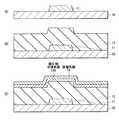
ここで、比較例を用いて薄膜トランジスタの伝達特性の劣化がチャネル保護膜により抑制されることを示す。図5(A)は、比較例1に係るバックチャネルエッチ構造の薄膜トランジスタ101の断面構造を表したものである。また、図5(B)は、比較例2に係るエッチストッパー構造の薄膜トランジスタ102の断面構造を表したものである。 Here, using a comparative example, it is shown that the deterioration of the transfer characteristics of the thin film transistor is suppressed by the channel protective film. FIG. 5A illustrates a cross-sectional structure of a
比較例1の薄膜トランジスタ101は、基板10上にゲート電極11,ゲート絶縁膜12,チャネル層13,ソース・ドレイン電極15A,15Bが積層された構造を有する。本実施の形態の薄膜トランジスタ1と比較すると、チャネル保護膜14A,14Bが設けられていない点において異なる。薄膜トランジスタ101では、酸化物半導体膜を島状に成形してチャネル層13を形成する際にフォトレジストが付着することにより、TFT特性の劣化が生じる虞があることが報告されている。 The
一方、比較例2の薄膜トランジスタ102は、薄膜トランジスタ101のチャネル層13上にエッチストッパー層104が設けられたものである。このエッチストッパー層104により、チャネル層13を形成する際の特性劣化を抑制することができる。しかし、薄膜トランジスタ102は、エッチストッパー層22を形成するために成膜,フォトリソグラフィーおよびエッチングの工程を行うため薄膜トランジスタ101と比較すると工程数が増加してしまう。 On the other hand, the
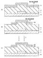
図6(A)は、実施例として実際に上述した製造方法によりチャネル保護膜14A,14Bを有する薄膜トランジスタ1を作製し、薄膜トランジスタの伝達特性を調べた結果を表したものである。その際、チャネル保護膜14A,14Bとしては厚み50nmのモリブデンからなる膜を用いた。なお、厚み10nmのモリブデンの場合も同様の結果が得られることを確認している。 FIG. 6A shows a result of manufacturing the thin film transistor 1 having the channel
一方、比較例1,2に係る薄膜トランジスタ101,102の伝達特性を調べた結果を図6(B)および図6(C)に示した。 On the other hand, the results of examining the transfer characteristics of the
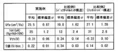
図7(A),図7(B)および図7(C)には、それぞれ図6(A),図6(B)および図6(C)の一部を拡大したものを示した。また、図8に実施例,比較例1および比較例2のTFTの特性パラメータを示した。図8においてUfeは移動度、Ionはオン出力電流、Vthはしきい値電圧、S値はサブスレッショルド係数を表す。 FIG. 7A, FIG. 7B, and FIG. 7C show enlarged parts of FIG. 6A, FIG. 6B, and FIG. 6C, respectively. FIG. 8 shows the characteristic parameters of the TFTs of Example, Comparative Example 1 and Comparative Example 2. In FIG. 8, Ufe represents mobility, Ion represents on-output current, Vth represents threshold voltage, and S value represents a subthreshold coefficient.
図7(A),図7(B)および図7(C)からわかるように、比較例1では、実施例や比較例2と比べ基板内で伝達特性のばらつきが見られるのに対し、実施例では比較例2と同程度の伝達特性が保持されている。 As can be seen from FIG. 7A, FIG. 7B, and FIG. 7C, the comparative example 1 shows a variation in the transfer characteristics in the substrate as compared with the example and the comparative example 2. In the example, the same transfer characteristic as in Comparative Example 2 is maintained.
図8において、移動度を表すUfe(cm2/Vs)に着目すると、比較例1は、比較例2に対して、Ufeの値が大きく下がる。一方、実施例は、比較例2と同程度に保たれ、更に、標準偏差σは、比較例2よりも小さい、すなわち基板面内ばらつきが小さいことがわかる。従って、これらの結果から薄膜トランジスタ1では、リソグラフィー工程を増やすことなく簡便な方法により、TFT特性(電界効果移動度とその基板面内ばらつき)の劣化を抑制することができることがわかった。In FIG. 8, focusing on Ufe (cm2 / Vs) representing mobility, the value of Ufe in Comparative Example 1 is significantly lower than that in Comparative Example 2. On the other hand, it can be seen that the example is kept at the same level as the comparative example 2, and the standard deviation σ is smaller than the comparative example 2, that is, the in-plane variation is small. Therefore, from these results, it was found that the thin film transistor 1 can suppress deterioration of TFT characteristics (field effect mobility and variations in the substrate surface thereof) by a simple method without increasing the number of lithography steps.
また、エッチストッパー構造の薄膜トランジスタ102は、エッチストッパー層104の大きさによりトランジスタサイズが決定するため、トランジスタサイズを小さくすることが困難であった。それに対し、薄膜トランジスタ1では、容易にトランジスタサイズを小さくすることができ、寄生容量を低減することも可能となる。 Further, since the transistor size of the
このように本実施の形態では、酸化物半導体膜13A,13Bを成形してチャネル層13を形成する際に、酸化物半導体膜13A,13Bを導電性膜14(チャネル保護膜14D)で覆うことにより、チャネル層13(酸化物半導体膜13A,13B)にフォトレジストによる化学物質が付着等することがなくなる。従って、得られた薄膜トランジスタ1では、伝達特性の劣化が抑制され、均一・良好なTFT特性を有するものとなり、信頼性が向上する。 Thus, in this embodiment, when the
更に、本実施の形態では、チャネル層を結晶酸化物半導体により形成するようにしたため、チャネル層とチャネル保護膜との間の選択的なエッチングを容易に行うことができる。 Further, in this embodiment mode, since the channel layer is formed using a crystalline oxide semiconductor, selective etching between the channel layer and the channel protective film can be easily performed.
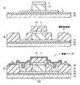
(変形例)
図9は、本発明の変形例に係る薄膜トランジスタ1Aの断面構成を表したものである。この薄膜トランジスタ1Aは、ソース・ドレイン電極15A,15Bが積層構造を有するものであり、チャネル保護膜14A,14Bが、ソース・ドレイン電極15A,15Bの積層構造のうちの最もチャネル層13に近い一層を構成している。チャネル保護膜14A,14B上には、金属膜17および金属膜18が積層されている。すなわち、ソース・ドレイン電極15Aは、チャネル保護膜14A,金属膜17および金属膜18の3層構造、ソース・ドレイン電極15Bは、チャネル保護膜14B,金属膜17および金属膜18の3層構造によりそれぞれ構成されている。(Modification)
FIG. 9 illustrates a cross-sectional configuration of a thin film transistor 1A according to a modification of the present invention. In this thin film transistor 1A, the source /
ボトムゲート型の薄膜トランジスタでは、ソース・ドレイン電極を積層構造により構成することが一般的である。図10に積層構造のソース・ドレイン電極を有する一般的な薄膜トランジスタ103の断面構造を示す。最も半導体層23に近い金属膜19は、半導体層23へ金属が拡散することを抑制し、または、半導体層23との電気的接合を安定化させる。また、最も半導体層23に遠い金属膜18は、金属膜19と金属膜18との間の金属膜17の熱のマイグレーションを抑制し、または、接合する導電体層との電気的接合を安定化させる。このような積層構造の組み合わせとして、例えば、モリブデン,アルミニウムおよびモリブデンの組み合わせや、チタン,アルミニウムおよびチタンの組み合わせが用いられる。 In the bottom gate type thin film transistor, the source / drain electrodes are generally formed of a laminated structure. FIG. 10 shows a cross-sectional structure of a general
薄膜トランジスタ1Aでは、チャネル保護膜14A,14Bがソース・ドレイン電極15A,15Bの一層を構成することにより、リソグラフィー工程やエッチング工程だけでなく成膜工程をも追加せずに良好な伝達特性の薄膜トランジスタを製造することが可能になる。その点を除き、薄膜トランジスタ1Aは上記第1の実施の形態の薄膜トランジスタ1と同様の構成を有し、その作用および効果も同様である。 In the thin film transistor 1A, the channel
薄膜トランジスタ1Aは、例えば、次のようにして製造することができる。まず、上記第1の実施の形態と同様にして、図2(A)ないし図3(A)に示した工程により、基板10に、ゲート電極11,ゲート絶縁膜12,チャネル層13およびチャネル保護膜14Dを形成する。例えばチャネル保護膜14Dはモリブデンにより構成する。次いで、チャネル保護膜14Dの上層に例えば、アルミニウム層およびモリブデン層を成膜した後、チャネル保護膜14D,アルミニウム層およびモリブデン層のエッチングを同時に行う。これにより、モリブデンからなるチャネル保護膜14A,14B、アルミニウムからなる金属膜17およびモリブデンからなる金属膜18によって構成されるソース・ドレイン電極15A,15Bが形成される。最後に第1の実施の形態と同様にして、保護膜16を設け、薄膜トランジスタ1Aが完成する。 The thin film transistor 1A can be manufactured, for example, as follows. First, in the same manner as in the first embodiment, the
薄膜トランジスタ1Aでは、酸化物半導体膜13A上に導電性膜14を積層しているが、後工程で導電性膜14はソース・ドレイン電極15を構成する1層となるため、成膜回数を増やすことなく製造することができる。また、一般的に酸化物半導体膜,ソース電極およびドレイン電極はスパッタリング法で成膜するため、薄膜トランジスタ1Aでは、酸化物半導体膜13Aおよび導電性膜14は連続スパッタで成膜することが可能である。 In the thin film transistor 1A, the
〔第2の実施の形態〕
図11および図12は、本発明の第2の実施の形態に係るトップゲート型(スタガ型)の薄膜トランジスタ2の製造方法を表したものである。薄膜トランジスタ2では、バッファ層20を有する基板10上にゲート電極11に対向してチャネル領域13Cを有するチャネル層13,ゲート絶縁膜12,ゲート電極11,層間絶縁膜21およびソース・ドレイン電極15A,15Bがこの順に積層されている。なお、この薄膜トランジスタ2では、上記第1の実施の形態と各構成要素同士の配置関係は異なるものの、それぞれの機能および構成材料は同様であるため、便宜上同一の符号を付し、適宜説明を省略する。[Second Embodiment]
11 and 12 show a method for manufacturing the top gate type (stagger type) thin film transistor 2 according to the second embodiment of the present invention. In the thin film transistor 2, a
次に、この薄膜トランジスタ2の製造方法を図11および図12により説明する。 Next, a method for manufacturing the thin film transistor 2 will be described with reference to FIGS.
図11(A)に示したように、シリコン酸化膜またはシリコン窒化膜などから構成されるバッファ層20を有する基板10上に、チャネル層13を構成する材料からなる酸化物半導体膜13Aおよび導電性の材料からなる導電性膜14をこの順に形成する。 As shown in FIG. 11A, an
次いで、導電性膜14および酸化物半導体膜13Aを例えばフォトリソグラフィーおよびエッチングの工程により図11(B)に示したように、島状に成形する。これによりチャネル保護膜14Dに覆われたチャネル層13が形成される。図4において説明したのと同様に酸化物半導体膜13Aに代えて、非晶質の酸化物半導体膜13Bを成膜してもよい(図示せず)。この導電性膜14および酸化物半導体膜13Bのエッチング後、かつ後述のチャネル保護膜14Dの除去(図11(C))前に、非晶質酸化物半導体から結晶酸化物半導体への変換を行い、チャネル層13を形成することが好ましい。 Next, the
チャネル層13を形成した後、図11(C)に示したようにチャネル保護膜14Dはエッチングにより除去しておく。 After the
チャネル保護膜14Dを除去した後、基板10およびチャネル層13の全面に、例えばプラズマCVD法によりゲート絶縁材料膜およびゲート電極材料膜を例えばスパッタリング法により形成し、例えばフォトリソグラフィーおよびエッチングによりゲート電極材料膜を成形してチャネル層13のチャネル領域13C上にゲート電極11を形成する。引き続き、ゲート電極11をマスクとしてゲート絶縁材料膜をエッチングすることによりゲート絶縁膜12を形成する。これにより図12(A)に示したように、チャネル層13のチャネル領域13C上に、ゲート絶縁膜12およびゲート電極11がこの順に形成される。なお、ゲート絶縁膜12およびゲート電極11は厚み以外が同一形状で形成される。 After removing the channel
続いて、基板10,ゲート電極11およびチャネル層13上の全面にわたって例えば、ポリイミドなどの有機絶縁膜,シリコン酸化膜またはシリコン窒化膜からなる層間絶縁膜21を形成し、図12(B)に示したように層間絶縁膜21に接続孔を設ける。層間絶縁膜21に代えて、保護膜16を用いてもよく、また、層間絶縁膜21の上層または下層に保護膜16を設けてもよい。 Subsequently, an
層間絶縁膜21に接続孔を設けた後、上記第1の実施の形態と同様にしてソース・ドレイン電極15A,15Bおよび保護膜16を形成する。層間絶縁膜21に代えて、保護膜16を用いた場合には、ソース・ドレイン電極15A,15B上の保護膜16を省略することも可能である。以上により図12(C)に示したトップゲート型の薄膜トランジスタ2が完成する。 After providing connection holes in the
この薄膜トランジスタ2の作用および効果は、第1の実施の形態と同様である。 The operation and effect of the thin film transistor 2 are the same as those in the first embodiment.
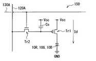
<適用例1>
図13は、薄膜トランジスタ1,1Aおよび薄膜トランジスタ2のいずれかを駆動素子として備えた表示装置の回路構成を表すものである。表示装置90は、例えば液晶ディスプレイや有機ELディスプレイなどであり、駆動パネル91上に、マトリクス状に配設された複数の画素10R,10G,10Bと、これらの画素10R,10G,10Bを駆動するための各種駆動回路とが形成されたものである。画素10R,10G,10Bはそれぞれ、赤色(R:Red ),緑色(G:Green )および青色(B:Blue)の色光を発する液晶表示素子や有機EL素子などである。これら3つの画素10R,10G,10Bを一つのピクセルとして、複数のピクセルにより表示領域110が構成されている。駆動パネル91上には、駆動回路として、例えば映像表示用のドライバである信号線駆動回路120および走査線駆動回路130と、画素駆動回路150とが配設されている。この駆動パネル91には、図示しない封止パネルが貼り合わせられ、この封止パネルにより画素10R,10G,10Bおよび上記駆動回路が封止されている。<Application example 1>
FIG. 13 illustrates a circuit configuration of a display device including any of the thin film transistors 1 and 1A and the thin film transistor 2 as a driving element. The
図14は、画素駆動回路150の等価回路図である。画素駆動回路150は、上記薄膜トランジスタ1,1Aおよび薄膜トランジスタ2のいずれかとして、トランジスタTr1,Tr2が配設されたアクティブ型の駆動回路である。トランジスタTr1,Tr2の間にはキャパシタCsが設けられ、第1の電源ライン(Vcc)および第2の電源ライン(GND)の間において、画素10R(または画素10G,10B)がトランジスタTr1に直列に接続されている。このような画素駆動回路150では、列方向に信号線120Aが複数配置され、行方向に走査線130Aが複数配置されている。各信号線120Aは、信号線駆動回路120に接続され、この信号線駆動回路120から信号線120Aを介してトランジスタTr2のソース電極に画像信号が供給されるようになっている。各走査線130Aは走査線駆動回路130に接続され、この走査線駆動回路130から走査線130Aを介してトランジスタTr2のゲート電極に走査信号が順次供給されるようになっている。この表示装置では、トランジスタTr1,Tr2が、上記実施の形態の薄膜トランジスタ1,1Aまたは薄膜トランジスタ2により構成されているので、均一・良好なTFT特性の薄膜トランジスタ1,1Aまたは薄膜トランジスタ2により高品質な表示が可能となる。このような表示装置90は、例えば次の適用例2〜6に示した電子機器に搭載することができる。 FIG. 14 is an equivalent circuit diagram of the
<適用例2>
図15は、テレビジョン装置の外観を表したものである。このテレビジョン装置は、例えば、フロントパネル310およびフィルターガラス320を含む映像表示画面部300を有している。<Application example 2>
FIG. 15 illustrates the appearance of a television device. The television apparatus includes a video display screen unit 300 including a front panel 310 and a filter glass 320, for example.
<適用例3>
図16は、デジタルスチルカメラの外観を表したものである。このデジタルスチルカメラは、例えば、フラッシュ用の発光部410、表示部420、メニュースイッチ430およびシャッターボタン440を有している。<Application example 3>
FIG. 16 shows the appearance of a digital still camera. The digital still camera has, for example, a flash light emitting unit 410, a display unit 420, a menu switch 430, and a
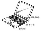
<適用例4>
図17は、ノート型パーソナルコンピュータの外観を表したものである。このノート型パーソナルコンピュータは、例えば、本体510,文字等の入力操作のためのキーボード520および画像を表示する表示部530を有している。<Application example 4>
FIG. 17 shows the appearance of a notebook personal computer. This notebook personal computer has, for example, a main body 510, a
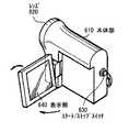
<適用例5>
図18は、ビデオカメラの外観を表したものである。このビデオカメラは、例えば、本体部610,この本体部610の前方側面に設けられた被写体撮影用のレンズ620,撮影時のスタート/ストップスイッチ630および表示部640を有している。<Application example 5>
FIG. 18 shows the appearance of the video camera. This video camera includes, for example, a main body 610, a
<適用例6>
図19は、携帯電話機の外観を表したものである。この携帯電話機は、例えば、上側筐体710と下側筐体720とを連結部(ヒンジ部)730で連結したものであり、ディスプレイ740,サブディスプレイ750,ピクチャーライト760およびカメラ770を有している。<Application example 6>
FIG. 19 shows the appearance of a mobile phone. For example, the mobile phone is obtained by connecting an
以上、実施の形態および変形例を挙げて本発明を説明したが、本発明は上記実施の形態等に限定されず、種々の変形が可能である。例えば上記実施の形態等では、ソース・ドレイン電極15A,15Bが3層からなる場合を例に挙げて説明したが、ソース・ドレイン電極15A,15Bは単層構造であってもよく、あるいは4層以上を積層した構造であってもよい。 Although the present invention has been described with reference to the embodiment and the modifications, the present invention is not limited to the above-described embodiment and the like, and various modifications can be made. For example, in the above-described embodiment, the case where the source /
また、例えば、上記実施の形態等において説明した各層の材料および厚み、または成膜方法および成膜条件などは限定されるものではなく、他の材料および厚みとしてもよく、または他の成膜方法および成膜条件としてもよい。 Further, for example, the material and thickness of each layer described in the above embodiment and the like, or the film formation method and film formation conditions are not limited, and other materials and thicknesses may be used, or other film formation methods. Alternatively, film forming conditions may be used.
1,1A,2・・・薄膜トランジスタ、10・・・基板、11・・・ゲート電極、12・・・ゲート絶縁膜、13・・・チャネル層、14A,14B・・・チャネル保護膜、15A,15B・・・ソース・ドレイン電極、16・・・保護膜、20・・・バッファ層、21・・・層間絶縁膜、90・・・表示装置、91・・・駆動パネル、10R,10G,10B・・・画素、110・・・表示領域、120・・・信号線駆動回路、130・・・走査線駆動回路、150・・・画素駆動回路、Tr1,Tr2・・・トランジスタ。DESCRIPTION OF SYMBOLS 1,1A, 2 ... Thin-film transistor, 10 ... Board | substrate, 11 ... Gate electrode, 12 ... Gate insulating film, 13 ... Channel layer, 14A, 14B ... Channel protective film, 15A, 15B ... Source / drain electrodes, 16 ... Protective film, 20 ... Buffer layer, 21 ... Interlayer insulating film, 90 ... Display device, 91 ... Drive panel, 10R, 10G, 10B ... Pixel, 110 ... Display area, 120 ... Signal line drive circuit, 130 ... Scan line drive circuit, 150 ... Pixel drive circuit, Tr1, Tr2 ... Transistor.
Claims (13)
Translated fromJapanese前記チャネル保護膜の前記ソース・ドレイン電極間の領域を前記導電性材料と結晶酸化物半導体との選択性を利用したエッチングにより除去する工程と
を含む薄膜トランジスタの製造方法。A channel layer made of an oxide semiconductor and a channel protective film made of a conductive material are formed on the gate electrode with a gate insulating film interposed therebetween, and then a pair of sources and drains are in contact with the channel protective film Forming an electrode;
Removing the region between the source and drain electrodes of the channel protective film by etching utilizing selectivity between the conductive material and the crystalline oxide semiconductor.
請求項1記載の薄膜トランジスタの製造方法。2. The channel layer is formed by forming an amorphous oxide semiconductor film on the gate insulating film and then converting the channel layer into a crystalline oxide semiconductor before forming the source / drain electrodes. A method for manufacturing a thin film transistor.
前記チャネル層の形成では、
前記金属膜の成膜前に、前記非晶質酸化物半導体から前記結晶酸化物半導体への変換を行う
請求項2記載の薄膜トランジスタの製造方法。After forming a metal film in contact with the channel protective film, the source / drain electrodes are formed by patterning the metal film,
In the formation of the channel layer,
The method for manufacturing a thin film transistor according to claim 2, wherein conversion from the amorphous oxide semiconductor to the crystalline oxide semiconductor is performed before forming the metal film.
請求項1記載の薄膜トランジスタの製造方法。The method for manufacturing a thin film transistor according to claim 1, wherein the channel layer is formed by forming a crystalline oxide semiconductor film over the gate insulating film.
時に行う
請求項1乃至4のうちいずれか1項記載の薄膜トランジスタの製造方法。5. The method of manufacturing a thin film transistor according to claim 1, wherein the step of forming the source / drain electrodes and the etching of the channel protective film are simultaneously performed.
ける少なくとも一層を兼ねている
請求項5記載の薄膜トランジスタの製造方法。6. The method of manufacturing a thin film transistor according to claim 5, wherein the source / drain electrodes have a laminated structure, and the channel protective film also serves as at least one layer in the laminated structure.
ングマスクとして、前記チャネル保護膜のエッチングを行う
請求項1乃至4のうちいずれか1項記載の薄膜トランジスタの製造方法。5. The method of manufacturing a thin film transistor according to claim 1, wherein after the step of forming the source / drain electrode, the channel protective film is etched using the source / drain electrode as an etching mask. 6.
前記チャネル保護膜を前記導電性材料と結晶酸化物半導体との選択性を利用したエッチングにより除去する工程と、
ゲート絶縁膜を間にして前記チャネル層上にゲート電極および前記チャネル層に接する一対のソース・ドレイン電極を形成する工程と
を含む薄膜トランジスタの製造方法。Forming a channel layer made of an oxide semiconductor and a channel protective film covering the channel layer and made of a conductive material;
Removing the channel protective film by etching utilizing the selectivity between the conductive material and the crystalline oxide semiconductor;
Forming a gate electrode and a pair of source / drain electrodes in contact with the channel layer on the channel layer with a gate insulating film interposed therebetween.
前記ゲート電極上にゲート絶縁膜を介して設けられた、結晶酸化物半導体よりなるチャネル層と、
導電性膜により構成され、前記チャネル層に接すると共に互いに電気的に分離された一対のチャネル保護膜と、
それぞれ前記チャネル保護膜を介して前記チャネル層に電気的に接続された一対のソース・ドレイン電極と
を備えた薄膜トランジスタ。A gate electrode;
A channel layer made of a crystalline oxide semiconductor provided on the gate electrode through a gate insulating film;
A pair of channel protective films made of a conductive film, in contact with the channel layer and electrically separated from each other;
A thin film transistor, comprising: a pair of source / drain electrodes electrically connected to the channel layer through the channel protective film.
一面を構成している
請求項9記載の薄膜トランジスタ。The thin film transistor according to claim 9, wherein opposed surfaces of the pair of source / drain electrodes constitute the same surface as opposed surfaces of the pair of channel protective films.
請求項9または10記載の薄膜トランジスタ。11. The thin film transistor according to claim 9, wherein end portions of the pair of channel protective films are formed at the same position as end portions of the channel layer.
n),銅(Cu)またはこれらの酸化物,窒化物あるいは酸窒化物からなる
請求項9または10記載の薄膜トランジスタ。The pair of channel protective films includes molybdenum (Mo), titanium (Ti), manganese (M
The thin film transistor according to claim 9 or 10, comprising n), copper (Cu), or an oxide, nitride or oxynitride thereof.
前記薄膜トランジスタは、
ゲート電極と、
前記ゲート電極上にゲート絶縁膜を介して設けられた、結晶酸化物半導体よりなるチャネル層と、
導電性膜により構成され、前記チャネル層に接すると共に互いに電気的に分離された一対のチャネル保護膜と、
それぞれ前記チャネル保護膜を介して前記チャネル層に電気的に接続された一対のソース・ドレイン電極と
を有する表示装置。A plurality of pixels and a thin film transistor for driving the plurality of pixels,
The thin film transistor
A gate electrode;
A channel layer made of a crystalline oxide semiconductor provided on the gate electrode through a gate insulating film;
A pair of channel protective films made of a conductive film, in contact with the channel layer and electrically separated from each other;
And a pair of source / drain electrodes electrically connected to the channel layer through the channel protective film.
Priority Applications (4)
| Application Number | Priority Date | Filing Date | Title |
|---|---|---|---|
| JP2011032207AJP5743064B2 (en) | 2011-02-17 | 2011-02-17 | THIN FILM TRANSISTOR, MANUFACTURING METHOD THEREOF, AND DISPLAY DEVICE |
| US13/365,780US20120211755A1 (en) | 2011-02-17 | 2012-02-03 | Thin film transistor, manufacturing method of thin film transistor and display |
| TW101104047ATWI493723B (en) | 2011-02-17 | 2012-02-08 | Thin film transistor, method and device for manufacturing thin film transistor |
| CN2012100290382ACN102646716A (en) | 2011-02-17 | 2012-02-09 | Thin film transistor, manufacturing method of thin film transistor, and display |
Applications Claiming Priority (1)
| Application Number | Priority Date | Filing Date | Title |
|---|---|---|---|
| JP2011032207AJP5743064B2 (en) | 2011-02-17 | 2011-02-17 | THIN FILM TRANSISTOR, MANUFACTURING METHOD THEREOF, AND DISPLAY DEVICE |
Publications (2)
| Publication Number | Publication Date |
|---|---|
| JP2012174723Atrue JP2012174723A (en) | 2012-09-10 |
| JP5743064B2 JP5743064B2 (en) | 2015-07-01 |
Family
ID=46652012
Family Applications (1)
| Application Number | Title | Priority Date | Filing Date |
|---|---|---|---|
| JP2011032207AActiveJP5743064B2 (en) | 2011-02-17 | 2011-02-17 | THIN FILM TRANSISTOR, MANUFACTURING METHOD THEREOF, AND DISPLAY DEVICE |
Country Status (4)
| Country | Link |
|---|---|
| US (1) | US20120211755A1 (en) |
| JP (1) | JP5743064B2 (en) |
| CN (1) | CN102646716A (en) |
| TW (1) | TWI493723B (en) |
Cited By (4)
| Publication number | Priority date | Publication date | Assignee | Title |
|---|---|---|---|---|
| WO2014061713A1 (en)* | 2012-10-17 | 2014-04-24 | Semiconductor Energy Laboratory Co., Ltd. | Semiconductor device |
| US9263259B2 (en) | 2012-10-17 | 2016-02-16 | Semiconductor Energy Laboratory Co., Ltd. | Semiconductor device comprising an oxide semiconductor |
| CN107564966A (en)* | 2017-08-07 | 2018-01-09 | 武汉华星光电半导体显示技术有限公司 | The manufacture method of thin film transistor (TFT) and thin film transistor (TFT), liquid crystal display panel |
| JP2018137475A (en)* | 2013-03-14 | 2018-08-30 | 株式会社半導体エネルギー研究所 | Semiconductor device manufacturing method |
Families Citing this family (15)
| Publication number | Priority date | Publication date | Assignee | Title |
|---|---|---|---|---|
| JP2719882B2 (en) | 1993-12-17 | 1998-02-25 | 住友ゴム工業株式会社 | Cleaning equipment |
| US9065009B2 (en)* | 2012-04-10 | 2015-06-23 | First Solar, Inc. | Apparatus and method for forming a transparent conductive oxide layer over a substrate using a laser |
| JP6204145B2 (en) | 2012-10-23 | 2017-09-27 | 株式会社半導体エネルギー研究所 | Semiconductor device |
| WO2014065343A1 (en) | 2012-10-24 | 2014-05-01 | Semiconductor Energy Laboratory Co., Ltd. | Semiconductor device |
| CN103887343B (en) | 2012-12-21 | 2017-06-09 | 北京京东方光电科技有限公司 | Thin film transistor (TFT) and preparation method thereof, array base palte and display device |
| CN103236443B (en)* | 2013-05-14 | 2014-05-14 | 广州新视界光电科技有限公司 | Metal oxide thin film transistor and preparation method thereof |
| US9006736B2 (en) | 2013-07-12 | 2015-04-14 | Semiconductor Energy Laboratory Co., Ltd. | Semiconductor device |
| CN103700705B (en)* | 2013-12-09 | 2017-07-28 | 深圳市华星光电技术有限公司 | A kind of IGZO electric crystals manufacture method |
| JP6227396B2 (en)* | 2013-12-20 | 2017-11-08 | 株式会社ジャパンディスプレイ | THIN FILM TRANSISTOR AND DISPLAY DEVICE USING THE SAME |
| TWI560882B (en)* | 2014-01-17 | 2016-12-01 | E Ink Holdings Inc | Semiconductor structure |
| CN103956386A (en)* | 2014-04-11 | 2014-07-30 | 京东方科技集团股份有限公司 | Thin film transistor, manufacturing method of thin film transistor, array substrate, manufacturing method of array substrate and display device |
| TWI566416B (en)* | 2014-12-01 | 2017-01-11 | 鴻海精密工業股份有限公司 | Thin film transistor substrate and method of fabricating same |
| CN106409686A (en)* | 2015-08-03 | 2017-02-15 | 中华映管股份有限公司 | Method for manufacturing oxide semiconductor thin film transistor |
| CN106298954B (en)* | 2016-08-31 | 2020-02-04 | 深圳市华星光电技术有限公司 | Thin film transistor and manufacturing method thereof |
| CN111755528A (en)* | 2020-07-31 | 2020-10-09 | 山东华芯半导体有限公司 | A flash memory cell and its manufacturing method |
Citations (4)
| Publication number | Priority date | Publication date | Assignee | Title |
|---|---|---|---|---|
| WO2007063966A1 (en)* | 2005-12-02 | 2007-06-07 | Idemitsu Kosan Co., Ltd. | Tft substrate and tft substrate manufacturing method |
| WO2008096768A1 (en)* | 2007-02-09 | 2008-08-14 | Idemitsu Kosan Co., Ltd. | Thin film transistor manufacturing method, thin film transistor, thin film transistor substrate and image display apparatus, image display apparatus and semiconductor device |
| WO2008126492A1 (en)* | 2007-04-05 | 2008-10-23 | Idemitsu Kosan Co., Ltd. | Field-effect transistor, and process for producing field-effect transistor |
| JP2010182929A (en)* | 2009-02-06 | 2010-08-19 | Fujifilm Corp | Manufacturing method of field effect transistor |
Family Cites Families (16)
| Publication number | Priority date | Publication date | Assignee | Title |
|---|---|---|---|---|
| JP3914266B2 (en)* | 1996-09-13 | 2007-05-16 | Tdk株式会社 | PTC thermistor material |
| JP3866070B2 (en)* | 2000-10-20 | 2007-01-10 | 株式会社 日立ディスプレイズ | Display device |
| US7141822B2 (en)* | 2001-02-09 | 2006-11-28 | Semiconductor Energy Laboratory Co., Ltd. | Semiconductor device and method for manufacturing the same |
| EP1770788A3 (en)* | 2005-09-29 | 2011-09-21 | Semiconductor Energy Laboratory Co., Ltd. | Semiconductor device having oxide semiconductor layer and manufacturing method thereof |
| CN101283388B (en)* | 2005-10-05 | 2011-04-13 | 出光兴产株式会社 | TFT substrate and method for manufacturing TFT substrate |
| JP5116290B2 (en)* | 2006-11-21 | 2013-01-09 | キヤノン株式会社 | Thin film transistor manufacturing method |
| JP5111867B2 (en)* | 2007-01-16 | 2013-01-09 | 株式会社ジャパンディスプレイイースト | Display device |
| KR101325053B1 (en)* | 2007-04-18 | 2013-11-05 | 삼성디스플레이 주식회사 | Thin film transistor substrate and manufacturing method thereof |
| TWI348766B (en)* | 2007-10-04 | 2011-09-11 | Taiwan Tft Lcd Ass | Method of fabricating thin film transistor |
| JP5427390B2 (en)* | 2007-10-23 | 2014-02-26 | 株式会社半導体エネルギー研究所 | Method for manufacturing semiconductor device |
| TWI469354B (en)* | 2008-07-31 | 2015-01-11 | Semiconductor Energy Lab | Semiconductor device and method of manufacturing same |
| JP2010123595A (en)* | 2008-11-17 | 2010-06-03 | Sony Corp | Thin film transistor and display |
| US8492756B2 (en)* | 2009-01-23 | 2013-07-23 | Semiconductor Energy Laboratory Co., Ltd. | Semiconductor device and method for manufacturing the same |
| JP5564331B2 (en)* | 2009-05-29 | 2014-07-30 | 株式会社半導体エネルギー研究所 | Method for manufacturing semiconductor device |
| KR101791370B1 (en)* | 2009-07-10 | 2017-10-27 | 가부시키가이샤 한도오따이 에네루기 켄큐쇼 | Semiconductor device |
| KR20190045396A (en)* | 2009-09-16 | 2019-05-02 | 가부시키가이샤 한도오따이 에네루기 켄큐쇼 | Transistor |
- 2011
- 2011-02-17JPJP2011032207Apatent/JP5743064B2/enactiveActive
- 2012
- 2012-02-03USUS13/365,780patent/US20120211755A1/ennot_activeAbandoned
- 2012-02-08TWTW101104047Apatent/TWI493723B/enactive
- 2012-02-09CNCN2012100290382Apatent/CN102646716A/enactivePending
Patent Citations (4)
| Publication number | Priority date | Publication date | Assignee | Title |
|---|---|---|---|---|
| WO2007063966A1 (en)* | 2005-12-02 | 2007-06-07 | Idemitsu Kosan Co., Ltd. | Tft substrate and tft substrate manufacturing method |
| WO2008096768A1 (en)* | 2007-02-09 | 2008-08-14 | Idemitsu Kosan Co., Ltd. | Thin film transistor manufacturing method, thin film transistor, thin film transistor substrate and image display apparatus, image display apparatus and semiconductor device |
| WO2008126492A1 (en)* | 2007-04-05 | 2008-10-23 | Idemitsu Kosan Co., Ltd. | Field-effect transistor, and process for producing field-effect transistor |
| JP2010182929A (en)* | 2009-02-06 | 2010-08-19 | Fujifilm Corp | Manufacturing method of field effect transistor |
Cited By (8)
| Publication number | Priority date | Publication date | Assignee | Title |
|---|---|---|---|---|
| WO2014061713A1 (en)* | 2012-10-17 | 2014-04-24 | Semiconductor Energy Laboratory Co., Ltd. | Semiconductor device |
| JP2014082390A (en)* | 2012-10-17 | 2014-05-08 | Semiconductor Energy Lab Co Ltd | Semiconductor device |
| US9263259B2 (en) | 2012-10-17 | 2016-02-16 | Semiconductor Energy Laboratory Co., Ltd. | Semiconductor device comprising an oxide semiconductor |
| US9287117B2 (en) | 2012-10-17 | 2016-03-15 | Semiconductor Energy Laboratory Co., Ltd. | Semiconductor device comprising an oxide semiconductor |
| US9812467B2 (en) | 2012-10-17 | 2017-11-07 | Semiconductor Energy Laboratory Co., Ltd. | Semiconductor device comprising an oxide semiconductor |
| TWI614897B (en)* | 2012-10-17 | 2018-02-11 | 半導體能源研究所股份有限公司 | Semiconductor device |
| JP2018137475A (en)* | 2013-03-14 | 2018-08-30 | 株式会社半導体エネルギー研究所 | Semiconductor device manufacturing method |
| CN107564966A (en)* | 2017-08-07 | 2018-01-09 | 武汉华星光电半导体显示技术有限公司 | The manufacture method of thin film transistor (TFT) and thin film transistor (TFT), liquid crystal display panel |
Also Published As
| Publication number | Publication date |
|---|---|
| US20120211755A1 (en) | 2012-08-23 |
| TWI493723B (en) | 2015-07-21 |
| TW201246554A (en) | 2012-11-16 |
| JP5743064B2 (en) | 2015-07-01 |
| CN102646716A (en) | 2012-08-22 |
Similar Documents
| Publication | Publication Date | Title |
|---|---|---|
| JP5743064B2 (en) | THIN FILM TRANSISTOR, MANUFACTURING METHOD THEREOF, AND DISPLAY DEVICE | |
| US20110215328A1 (en) | Thin film transistor, method of manufacturing the thin film transistor, and display device | |
| JP5668917B2 (en) | Thin film transistor and manufacturing method thereof | |
| US8748882B2 (en) | Thin film transistor, electronic device, display device, and method of manufacturing thin film transistor | |
| TWI455320B (en) | Thin film transistor and manufacturing method thereof, and display device | |
| JP2012015436A (en) | Thin film transistor and display device | |
| JP2010182819A (en) | Thin-film transistor, and display device | |
| JP2012160679A (en) | Thin-film transistor, display device, and electronic apparatus | |
| JP2010182818A (en) | Thin-film transistor, and display device | |
| JP2014229814A (en) | Thin-film transistor, display device, and electronic apparatus | |
| US8816352B2 (en) | Display device and electronic device | |
| JP2014170829A (en) | Semiconductor device, manufacturing method of the same, display device manufacturing method, and electronic apparatus manufacturing method | |
| CN103208527B (en) | Thin film transistor, method of manufacturing thin film transistor, display, and electronic apparatus | |
| JP2012204548A (en) | Display device and manufacturing method therefor | |
| JP2013206919A (en) | Thin film transistor, manufacturing method of the same and display device | |
| JP6019330B2 (en) | THIN FILM TRANSISTOR, METHOD FOR PRODUCING THIN FILM TRANSISTOR, DISPLAY DEVICE, AND ELECTRONIC DEVICE | |
| US9502492B2 (en) | Semiconductor device, method of manufacturing the same, display unit, and electronic apparatus | |
| US9219084B2 (en) | Display device including a thin film transistor having wiring and electrodes with different ionization tendencies | |
| US9178074B2 (en) | Semiconductor device, display unit, and electronic apparatus |
Legal Events
| Date | Code | Title | Description |
|---|---|---|---|
| A621 | Written request for application examination | Free format text:JAPANESE INTERMEDIATE CODE: A621 Effective date:20140107 | |
| A977 | Report on retrieval | Free format text:JAPANESE INTERMEDIATE CODE: A971007 Effective date:20141225 | |
| A131 | Notification of reasons for refusal | Free format text:JAPANESE INTERMEDIATE CODE: A131 Effective date:20150113 | |
| A521 | Request for written amendment filed | Free format text:JAPANESE INTERMEDIATE CODE: A523 Effective date:20150218 | |
| TRDD | Decision of grant or rejection written | ||
| A01 | Written decision to grant a patent or to grant a registration (utility model) | Free format text:JAPANESE INTERMEDIATE CODE: A01 Effective date:20150331 | |
| A711 | Notification of change in applicant | Free format text:JAPANESE INTERMEDIATE CODE: A712 Effective date:20150327 | |
| A61 | First payment of annual fees (during grant procedure) | Free format text:JAPANESE INTERMEDIATE CODE: A61 Effective date:20150421 | |
| R150 | Certificate of patent or registration of utility model | Ref document number:5743064 Country of ref document:JP Free format text:JAPANESE INTERMEDIATE CODE: R150 | |
| R250 | Receipt of annual fees | Free format text:JAPANESE INTERMEDIATE CODE: R250 | |
| R250 | Receipt of annual fees | Free format text:JAPANESE INTERMEDIATE CODE: R250 | |
| R250 | Receipt of annual fees | Free format text:JAPANESE INTERMEDIATE CODE: R250 | |
| R250 | Receipt of annual fees | Free format text:JAPANESE INTERMEDIATE CODE: R250 | |
| R250 | Receipt of annual fees | Free format text:JAPANESE INTERMEDIATE CODE: R250 | |
| S303 | Written request for registration of pledge or change of pledge | Free format text:JAPANESE INTERMEDIATE CODE: R316303 | |
| R350 | Written notification of registration of transfer | Free format text:JAPANESE INTERMEDIATE CODE: R350 | |
| R250 | Receipt of annual fees | Free format text:JAPANESE INTERMEDIATE CODE: R250 | |
| S803 | Written request for registration of cancellation of provisional registration | Free format text:JAPANESE INTERMEDIATE CODE: R316803 | |
| R350 | Written notification of registration of transfer | Free format text:JAPANESE INTERMEDIATE CODE: R350 | |
| S111 | Request for change of ownership or part of ownership | Free format text:JAPANESE INTERMEDIATE CODE: R313113 | |
| R350 | Written notification of registration of transfer | Free format text:JAPANESE INTERMEDIATE CODE: R350 | |
| R250 | Receipt of annual fees | Free format text:JAPANESE INTERMEDIATE CODE: R250 | |
| R250 | Receipt of annual fees | Free format text:JAPANESE INTERMEDIATE CODE: R250 | |
| S111 | Request for change of ownership or part of ownership | Free format text:JAPANESE INTERMEDIATE CODE: R313113 | |
| R350 | Written notification of registration of transfer | Free format text:JAPANESE INTERMEDIATE CODE: R350 |