JP2012161077A - Pre-emphasis circuit and differential current signal transmission system - Google Patents
Pre-emphasis circuit and differential current signal transmission systemDownload PDFInfo
- Publication number
- JP2012161077A JP2012161077AJP2012011901AJP2012011901AJP2012161077AJP 2012161077 AJP2012161077 AJP 2012161077AJP 2012011901 AJP2012011901 AJP 2012011901AJP 2012011901 AJP2012011901 AJP 2012011901AJP 2012161077 AJP2012161077 AJP 2012161077A
- Authority
- JP
- Japan
- Prior art keywords
- emphasis
- differential
- signal
- control signal
- output
- Prior art date
- Legal status (The legal status is an assumption and is not a legal conclusion. Google has not performed a legal analysis and makes no representation as to the accuracy of the status listed.)
- Granted
Links
- 230000008054signal transmissionEffects0.000titleclaimsabstractdescription46
- 230000007274generation of a signal involved in cell-cell signalingEffects0.000claimsdescription39
- 230000003111delayed effectEffects0.000claimsdescription25
- 230000001934delayEffects0.000claimsdescription6
- 230000003071parasitic effectEffects0.000abstractdescription8
- 239000003990capacitorSubstances0.000abstractdescription4
- 238000010586diagramMethods0.000description19
- 230000005540biological transmissionEffects0.000description17
- 230000000630rising effectEffects0.000description9
- 238000000034methodMethods0.000description5
- 230000000694effectsEffects0.000description4
- 230000002238attenuated effectEffects0.000description2
- 230000002411adverseEffects0.000description1
- 238000012986modificationMethods0.000description1
- 230000004048modificationEffects0.000description1
- 230000011664signalingEffects0.000description1
Images


Classifications
- H—ELECTRICITY
- H03—ELECTRONIC CIRCUITRY
- H03K—PULSE TECHNIQUE
- H03K19/00—Logic circuits, i.e. having at least two inputs acting on one output; Inverting circuits
- H03K19/0175—Coupling arrangements; Interface arrangements
- H—ELECTRICITY
- H03—ELECTRONIC CIRCUITRY
- H03K—PULSE TECHNIQUE
- H03K17/00—Electronic switching or gating, i.e. not by contact-making and –breaking
- H03K17/16—Modifications for eliminating interference voltages or currents
- H03K17/161—Modifications for eliminating interference voltages or currents in field-effect transistor switches
- H03K17/162—Modifications for eliminating interference voltages or currents in field-effect transistor switches without feedback from the output circuit to the control circuit
- H—ELECTRICITY
- H03—ELECTRONIC CIRCUITRY
- H03K—PULSE TECHNIQUE
- H03K5/00—Manipulating of pulses not covered by one of the other main groups of this subclass
- H03K5/15—Arrangements in which pulses are delivered at different times at several outputs, i.e. pulse distributors
- H03K5/151—Arrangements in which pulses are delivered at different times at several outputs, i.e. pulse distributors with two complementary outputs
- H03K5/1515—Arrangements in which pulses are delivered at different times at several outputs, i.e. pulse distributors with two complementary outputs non-overlapping
- H—ELECTRICITY
- H04—ELECTRIC COMMUNICATION TECHNIQUE
- H04L—TRANSMISSION OF DIGITAL INFORMATION, e.g. TELEGRAPHIC COMMUNICATION
- H04L25/00—Baseband systems
- H04L25/02—Details ; arrangements for supplying electrical power along data transmission lines
- H—ELECTRICITY
- H04—ELECTRIC COMMUNICATION TECHNIQUE
- H04L—TRANSMISSION OF DIGITAL INFORMATION, e.g. TELEGRAPHIC COMMUNICATION
- H04L25/00—Baseband systems
- H04L25/02—Details ; arrangements for supplying electrical power along data transmission lines
- H04L25/03—Shaping networks in transmitter or receiver, e.g. adaptive shaping networks
- H04L25/03006—Arrangements for removing intersymbol interference
- H04L25/03343—Arrangements at the transmitter end
Landscapes
- Engineering & Computer Science (AREA)
- Signal Processing (AREA)
- Physics & Mathematics (AREA)
- Power Engineering (AREA)
- Computer Networks & Wireless Communication (AREA)
- Computer Hardware Design (AREA)
- Nonlinear Science (AREA)
- Computing Systems (AREA)
- General Engineering & Computer Science (AREA)
- Mathematical Physics (AREA)
- Logic Circuits (AREA)
- Dc Digital Transmission (AREA)
- Cable Transmission Systems, Equalization Of Radio And Reduction Of Echo (AREA)
Abstract
Description
Translated fromJapanese本発明は、信号伝送システムに使用されるプリエンファシス回路に関する。 The present invention relates to a pre-emphasis circuit used in a signal transmission system.
従来より、差動伝送線路対(differential transmission line pair)を介して差動電流信号を送信し、伝達された信号を受信端で感知する差動電流駆動方式の信号伝送システムに対する研究が進められてきた。 Conventionally, research on a differential current drive type signal transmission system in which a differential current signal is transmitted through a differential transmission line pair and the transmitted signal is sensed at a receiving end has been advanced. It was.
差動電流駆動方式は送信部で送信しようとするデータに対応する互いに異なる大きさの電流を生成させて2個の伝送ラインを介して伝送するようになり、受信端では2個の伝送ラインに流れる電流の差を利用してデータを復元する。 In the differential current driving method, currents of different magnitudes corresponding to data to be transmitted by the transmission unit are generated and transmitted through two transmission lines, and at the receiving end, the two transmission lines are transmitted. Data is restored by using the difference between the flowing currents.
このような差動電流駆動方式の信号伝送システムでは送信端で損失のあるチャネルを介してデジタル信号を伝送する時に、受信端では伝送された信号がチャネルの周波数特性により歪曲された状態で受信される。一般に、損失のあるチャネルは高周波領域でより多くの損失を出すため、このようなチャネルを介して伝送される信号の高周波成分が低周波成分に比べてより多く減衰される。デジタル信号で高周波成分は主に信号の電圧レベルが速やかに変わる部分、すなわち立ち上がりエッジや立ち下がりエッジに該当する。 In such a differential current drive type signal transmission system, when a digital signal is transmitted through a lossy channel at the transmitting end, the transmitted signal is received in a distorted state due to the frequency characteristics of the channel at the receiving end. The In general, a lossy channel causes more loss in the high frequency region, so that the high frequency component of the signal transmitted through such a channel is attenuated more than the low frequency component. The high frequency component in the digital signal mainly corresponds to a portion where the voltage level of the signal changes rapidly, that is, a rising edge or a falling edge.
したがって、損失のあるチャネルを通過した信号は元の波形より歪んだ波形を持つようになり周波数毎に伝送される信号が到着する時間が変わることがあり、その結果多くのジッタが発生することがあり、全体的にタイミングマージンも大きく減ることがある。 Therefore, a signal that has passed through a lossy channel has a waveform that is distorted from the original waveform, and the time at which the signal transmitted for each frequency arrives may change, resulting in a lot of jitter. In general, the timing margin may be greatly reduced.
このような問題点を解決するために、周波数帯域毎に信号を強調するか、抑制することによってチャネルを通過する間に歪曲される信号を補償して最終的に受信端で元の信号を受信できるように信号の波形を調節する方法にプリエンファシス(Pre−emphasis)技法が使用される。 In order to solve such problems, the signal that is distorted while passing through the channel is compensated by emphasizing or suppressing the signal for each frequency band, and finally the original signal is received at the receiving end. A pre-emphasis technique is used to adjust the waveform of the signal as possible.
プリエンファシス技法は送信端で信号を送信する前に信号の高周波帯域を所定量だけ予め補強し、補強された信号を送信する方法である。以上で説明したように、信号の高周波成分は主に立ち上がりエッジ(rising edge)や立ち下がりエッジ(falling edge)で現れるが、プリエンファシス技法はエッジ部分で信号の大きさをチャネルで減衰される分だけ増やすことであるといえる。 The pre-emphasis technique is a method in which a high-frequency band of a signal is reinforced in advance by a predetermined amount before transmitting a signal at a transmission end, and the reinforced signal is transmitted. As described above, the high-frequency component of the signal mainly appears at the rising edge or the falling edge, but the pre-emphasis technique is such that the signal size is attenuated by the channel at the edge portion. It can be said that it is only increasing.
図1は、従来技術による差動信号駆動方式の出力ドライバに形成されたプリエンファシス回路を示す図である。 FIG. 1 is a diagram showing a pre-emphasis circuit formed in a differential signal driving type output driver according to the prior art.
図1を参照すると、従来技術によるプリエンファシス回路は第1プリエンファシス回路110と第2プリエンファシス回路130とで構成される。 Referring to FIG. 1, the conventional pre-emphasis circuit includes a first
第1プリエンファシス回路110は第1電圧VDDと第2電圧GNDの間の範囲で動作する4個のスイッチングトランジスタ111〜114で構成される。2個のスイッチングトランジスタ111、112はPMOSトランジスタに第1電圧VDDを出力ドライバ120に伝達する二端子のソース(source)として動作し、2個のスイッチングトランジスタ113、114はNMOSトランジスタで出力ドライバ120の出力電圧を抑制する二端子のシンク(sink)として動作する。 The first
第2プリエンファシス回路130は第1電圧VDDと第2電圧GNDの間の範囲で動作する4個のスイッチングトランジスタ131〜134で構成される。2個のスイッチングトランジスタ131、132はPMOSトランジスタで第1電圧VDDを出力ドライバ120に伝達する二端子のソースとして動作し、2個のスイッチングトランジスタ133、134はNMOSトランジスタで出力ドライバ120の出力電圧を抑制する二端子のシンクとして動作する。 The second
プリエンファシス回路が効率的に動作するためにはソースとして動作する時にはソースとしてのみ動作し、シンクとして動作する時にはシンクとしてのみ動作しなければならない。 In order for the pre-emphasis circuit to operate efficiently, it must operate only as a source when operating as a source, and only operate as a sink when operating as a sink.
しかし、図1に示すプリエンファシス回路の場合、2個の入力信号IN1、IN2を使用して4個のトランジスタを制御することによってソース動作又はシンク動作時に望まない電流が流れてプリエンファシス効果を半減させる原因になる。 However, in the case of the pre-emphasis circuit shown in FIG. 1, by controlling the four transistors using the two input signals IN1 and IN2, an undesired current flows during source operation or sink operation, and the pre-emphasis effect is reduced by half. Cause it.
図2は、従来技術によるプリエンファシス回路のスイッチングトランジスタに流れる電流を示す図である。 FIG. 2 is a diagram illustrating a current flowing through a switching transistor of a pre-emphasis circuit according to the related art.
図2の(a)はソースとして動作するスイッチングトランジスタ112に流れる電流を示す図で、図2の(b)はシンクとして動作するスイッチングトランジスタ113に流れる電流を示す図である。 2A is a diagram showing a current flowing through the
図2を参照すると、従来技術によるプリエンファシス回路はソースとして動作するスイッチングトランジスタ112とシンクとして動作するスイッチングトランジスタ113でソース電流及びシンク電流が同時に流れることがわかる。 Referring to FIG. 2, it can be seen that in the pre-emphasis circuit according to the prior art, a source current and a sink current simultaneously flow in the
このように従来技術によるプリエンファシス回路は2個の入力信号IN1、IN2を使用して4個のトランジスタを制御することによってソースとシンクをそれぞれ制御することができない。したがって、ソースとして動作するトランジスタにシンク電流が流れ、シンクとして動作するトランジスタにソース電流が流れてプリエンファシス効果が半減される問題がある。 As described above, the pre-emphasis circuit according to the prior art cannot control the source and the sink by controlling the four transistors using the two input signals IN1 and IN2. Therefore, there is a problem that the sink current flows through the transistor operating as the source, and the source current flows through the transistor operating as the sink, so that the pre-emphasis effect is halved.
また、従来のプリエンファシス回路は4個のトランジスタを使用することによってトランジスタによる寄生抵抗及び寄生キャパシタ値により負荷(load)値が増加してスイッチング速度が遅くなる短所がある。 Also, the conventional pre-emphasis circuit has a disadvantage in that the use of four transistors increases the load value due to the parasitic resistance and parasitic capacitor values of the transistors, thereby slowing the switching speed.
一方、従来のプリエンファシス回路は予め決められた遅延時間によってプリエンファシス電流の供給時間が決定されるため伝送線の負荷値によって過度のプリエンファシスが適用されることもあり、過少のプリエンファシスが適用されることもあるのでプリエンファシス電流を能動的に調節して供給することが難しい問題がある。 On the other hand, in the conventional pre-emphasis circuit, since the pre-emphasis current supply time is determined by a predetermined delay time, excessive pre-emphasis may be applied depending on the load value of the transmission line. In some cases, it is difficult to actively adjust and supply the pre-emphasis current.
本発明が達成しようとする技術的課題は、プリエンファシス回路を動作させるために必要なスイッチングトランジスタの数を減らして寄生抵抗及び寄生キャパシタを減少させ、それぞれのスイッチングトランジスタを制御するそれぞれのプリエンファシス制御信号を供給することによって望まない電流の発生を防止できるプリエンファシス回路及びこれを備えた差動電流信号伝送システムを提供することにある。 The technical problem to be achieved by the present invention is to reduce the number of switching transistors required to operate a pre-emphasis circuit, to reduce parasitic resistance and parasitic capacitor, and to control each switching transistor. An object of the present invention is to provide a pre-emphasis circuit capable of preventing generation of an undesired current by supplying a signal and a differential current signal transmission system including the same.
上記技術的課題を達成するための本発明によるプリエンファシス回路は、差動入力信号の論理演算で生成された第1乃至第4プリエンファシス制御信号に応じて出力ドライバの出力ノードにプリエンファシス出力電流を伝達するプリエンファシス回路であって、第1電圧VDD及び第2電圧GNDの範囲で駆動され、前記第1プリエンファシス制御信号Con1及び第2プリエンファシス制御信号Con2に応じて生成した第1プリエンファシス出力電流を前記出力ドライバの第1出力ノードN1に出力する第1プリエンファシス回路及び前記第1電圧VDD及び第2電圧GNDの範囲で駆動され、前記第3プリエンファシス制御信号Con3及び第4プリエンファシス制御信号Con4に応じて生成した第2プリエンファシス出力電流を前記出力ドライバの第2出力ノードN2に出力する第2プリエンファシス回路を含むことを特徴とする。 A pre-emphasis circuit according to the present invention for achieving the above technical problem includes a pre-emphasis output current at an output node of an output driver according to first to fourth pre-emphasis control signals generated by a logical operation of a differential input signal. A first pre-emphasis circuit that is driven in a range of a first voltage VDD and a second voltage GND and is generated according to the first pre-emphasis control signal Con1 and the second pre-emphasis control signal Con2. A first pre-emphasis circuit that outputs an output current to the first output node N1 of the output driver, and the third pre-emphasis control signal Con3 and the fourth pre-emphasis are driven in the range of the first voltage VDD and the second voltage GND. The second pre-emphasis output current generated according to the control signal Con4 Characterized in that it comprises a second pre-emphasis circuit to be output to the second output node N2 of the output driver.
上記他の技術的課題を達成するための本発明の一実施例によるプリエンファシス回路を備えた差動電流信号伝送システムは、差動入力信号INP、INNを入力されて、遅延された差動入力信号D_INP、D_INN及びプリエンファシス制御信号Con1〜Con4を生成するプリエンファシス制御信号生成部、前記遅延された差動入力信号D_INP、D_INNに応じて生成した出力信号OUTP、OUTNを出力ノードN1、N2に出力する出力ドライバ及び前記プリエンファシス制御信号Con1〜Con4に応じて生成したプリエンファシス出力電流を前記出力ノードN1、N2に出力するプリエンファシス回路を含むことを特徴とする。 A differential current signal transmission system including a pre-emphasis circuit according to an embodiment of the present invention for achieving the above other technical problems is provided with a differential input that receives a differential input signal INP and INN and is delayed. A pre-emphasis control signal generator for generating signals D_INP and D_INN and pre-emphasis control signals Con1 to Con4, and output signals OUTP and OUTN generated according to the delayed differential input signals D_INP and D_INN to output nodes N1 and N2, respectively. An output driver for outputting and a pre-emphasis circuit for outputting a pre-emphasis output current generated in response to the pre-emphasis control signals Con1 to Con4 to the output nodes N1 and N2.
上記他の技術的課題を達成するための本発明の他の実施例によるプリエンファシス回路を備えた差動電流信号伝送システムは、差動入力信号INP、INN及び差動制御信号Con_P、Con_Nを入力されて、遅延された差動入力信号D_INP、D_INN及びプリエンファシス制御信号Con1〜Con4を生成するプリエンファシス制御信号生成部、前記遅延された差動入力信号に応じて出力信号OUTP、OUTNを生成して出力ノードに出力する出力ドライバ、前記プリエンファシス制御信号Con1〜Con4に応じて生成したプリエンファシス出力電流を前記出力ノードに出力するプリエンファシス回路、高電源電圧VHである基準電圧を生成して出力するダミー部及び前記出力信号OUTP、OUTN及び前記基準電圧を比較して前記差動制御信号Con_P、Con_Nを生成して前記プリエンファシス制御信号生成部に提供する比較部を含むことを特徴とする。 A differential current signal transmission system having a pre-emphasis circuit according to another embodiment of the present invention for achieving the other technical problems described above receives differential input signals INP and INN and differential control signals Con_P and Con_N. A pre-emphasis control signal generator for generating delayed differential input signals D_INP and D_INN and pre-emphasis control signals Con1 to Con4, and generating output signals OUTP and OUTN according to the delayed differential input signals. An output driver that outputs to the output node, a pre-emphasis circuit that outputs the pre-emphasis output current generated according to the pre-emphasis control signals Con1 to Con4 to the output node, and generates and outputs a reference voltage that is the high power supply voltage VH Dummy section, the output signals OUTP, OUTN and the reference voltage Wherein compared to a differential control signal Con_P, characterized in that it comprises a comparison unit which generates and provides Con_N to the pre-emphasis control signal generation unit.
本発明によるプリエンファシス回路及びこれを備えた差動電流信号伝送システムによれば、回路の動作に必要なスイッチングトランジスタの数を減らすことによってトランジスタによる寄生抵抗及び寄生キャパシタを減少させることができ、これによりスイッチング速度を向上させることができる長所がある。 According to the pre-emphasis circuit and the differential current signal transmission system including the pre-emphasis circuit according to the present invention, the parasitic resistance and the parasitic capacitor due to the transistor can be reduced by reducing the number of switching transistors necessary for the operation of the circuit. Therefore, the switching speed can be improved.
また、それぞれのプリエンファシス制御信号を介してそれぞれのスイッチングトランジスタを制御することによって望まない電流の発生を防止し、プリエンファシス出力電流を能動的に調節して供給することによってプリエンファシス性能をより一層向上させることができる効果がある。 In addition, by controlling each switching transistor via each pre-emphasis control signal, generation of undesired current is prevented, and pre-emphasis performance is further improved by actively adjusting and supplying the pre-emphasis output current. There is an effect that can be improved.
以下、添付された図面を参照して本発明の好ましい実施例をより詳細に説明する。本明細書を説明する過程で用いられる数字、例えば、第1、第2などは同一又は類似の個体を区分するための識別記号に過ぎないものである。 Hereinafter, exemplary embodiments of the present invention will be described in detail with reference to the accompanying drawings. The numbers used in the description of the present specification, such as first and second, are merely identification symbols for distinguishing the same or similar individuals.
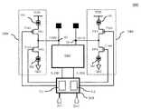
図3は、本発明の一実施例によるプリエンファシス回路を備えた差動電流信号伝送システムの構成を示す図である。 FIG. 3 is a diagram illustrating a configuration of a differential current signal transmission system including a pre-emphasis circuit according to an embodiment of the present invention.
図3を参考すると、本発明の一実施例によるプリエンファシス回路を備えた差動電流信号伝送システムは、プリエンファシス制御信号生成部310、出力ドライバ320及びプリエンファシス回路330、340を具備する。 Referring to FIG. 3, a differential current signal transmission system including a pre-emphasis circuit according to an embodiment of the present invention includes a pre-emphasis
前記プリエンファシス制御信号生成部310は差動入力信号INP、INNを入力されて遅延された差動入力信号D_INP、D_INNを生成する遅延回路311と、差動入力信号INP、INNを論理演算してプリエンファシス制御信号Con1〜Con4を生成する制御信号生成回路312と、を含む。 The pre-emphasis
前記出力ドライバ320は遅延された差動入力信号D_INP、D_INNに応じて出力信号OUTP、OUTNを生成して出力ノードN1、N2にそれぞれ出力する。 The
前記プリエンファシス回路330、340は第1プリエンファシス回路330及び第2プリエンファシス回路340を含み、プリエンファシス制御信号生成部310で生成されたプリエンファシス制御信号Con1〜Con4に応じてプリエンファシス出力電流を生成して出力ノードN1、N2に出力する。 The
第1プリエンファシス回路330は第1電圧VDD及び第2電圧GNDの範囲で駆動され第1プリエンファシス制御信号Con1及び第2プリエンファシス制御信号Con2に応じて第1プリエンファシス出力電流を生成して第1出力ノードN1に出力する。第1プリエンファシス回路330は第1スイッチSW1及び第2スイッチSW2を具備する。第1スイッチSW1は第1端子が第1電圧VDDに連結され、第2端子が第1出力ノードN1に連結され、制御端子に第1プリエンファシス制御信号Con1が印加される。第2スイッチSW2は第1端子が第1出力ノードN1に連結され、第2端子が第2電圧GNDに連結され、制御端子に第2プリエンファシス制御信号Con2が印加される。 The
第2プリエンファシス回路340は第1電圧VDD及び第2電圧GNDの範囲で駆動され第3プリエンファシス制御信号con3及び第4プリエンファシス制御信号Con4に応じて第2プリエンファシス出力電流を生成して第2出力ノードN2に出力する。第2プリエンファシス回路340は第3スイッチSW3及び第4スイッチSW4を具備する。第3スイッチSW3は第1端子が第1電圧VDDに連結され、第2端子が第2出力ノードN2に連結され、制御端子に第3プリエンファシス制御信号Con3が印加される。第4スイッチSW4は第1端子が第2出力ノードN2に連結され、第2端子が第2電圧GNDに連結され、制御端子に第4プリエンファシス制御信号Con4が印加される。 The
第1スイッチSW1及び第4スイッチSW4と第2スイッチSW2及び第3スイッチSW3は互いに相補的に動作する。すなわち、第1スイッチSW1及び第4スイッチSW4がターンオンされる時、第2スイッチSW2及び第3スイッチSW3はターンオフされる。第1スイッチSW1及び第4スイッチSW4がターンオンされる時、第2スイッチSW2及び第3スイッチSW3はターンオンされる。第1スイッチSW1乃至第4スイッチSW4はMOSトランジスタに具現され得るが、これに限定されるものではない。 The first switch SW1, the fourth switch SW4, the second switch SW2, and the third switch SW3 operate complementarily to each other. That is, when the first switch SW1 and the fourth switch SW4 are turned on, the second switch SW2 and the third switch SW3 are turned off. When the first switch SW1 and the fourth switch SW4 are turned on, the second switch SW2 and the third switch SW3 are turned on. The first to fourth switches SW1 to SW4 may be implemented as MOS transistors, but are not limited thereto.
図4は、本発明の他の実施例によるプリエンファシス回路及びこれを備えた差動電流信号伝送システムの構成を示す図である。 FIG. 4 is a diagram illustrating a configuration of a pre-emphasis circuit and a differential current signal transmission system including the pre-emphasis circuit according to another embodiment of the present invention.
図4に示すように、本発明の他の実施例によるプリエンファシス回路330、340は必要に応じて第1スイッチSW1乃至第4スイッチSW4の端子と第1電圧VDD又は第2電圧GNDの間に定電流源331、332、341、342を連結して一定の電流を供給することもできる。 As shown in FIG. 4, the
すなわち、本発明の他の実施例によるプリエンファシス回路は、図3のプリエンファシス回路に第1電流源331乃至第4電流源342をさらに具備できる。第1電流源331は第1スイッチSW1の第1端子及び第1電圧VDDの間に形成され、第2電流源332は第2スイッチSW2の第2端子及び第2電圧GNDの間に形成される。第3電流源341は第3スイッチSW3の第1端子及び第1電圧VDDの間に形成され、第4電流源342は第4スイッチSW4の第2端子及び第2電圧GNDの間に形成される。第1スイッチSW1乃至第4スイッチSW4はMOSトランジスタに具現され得る。 That is, the pre-emphasis circuit according to another embodiment of the present invention may further include a first current source 331 to a fourth
その他プリエンファシス制御信号生成部310、出力ドライバ320、第1プリエンファシス回路330、第2プリエンファシス回路340などは図3の説明から当業者が容易に理解できるものであるので詳細な説明は省略する。 Other details of the pre-emphasis control
図5は、本発明の実施例によるプリエンファシス回路のスイッチに流れる電流を示す図である。 FIG. 5 is a diagram illustrating a current flowing through the switch of the pre-emphasis circuit according to the embodiment of the present invention.
図5の(a)はソースとして動作する第1スイッチSW1に流れる電流を示す図で、図2の(b)はシンクとして動作する第2スイッチSW2に流れる電流を示す図である。
図5を図2と比較してみてみると、本発明の実施例によるプリエンファシス回路の場合、第1スイッチSW1及び第2スイッチSW2はそれぞれ一つずつの制御信号により動作するのでソースとして動作する場合又はシンクとして動作する場合、他方のスイッチには不要な電流が流れないことがわかる。FIG. 5A is a diagram showing a current flowing through the first switch SW1 operating as a source, and FIG. 2B is a diagram showing a current flowing through the second switch SW2 operating as a sink.
Comparing FIG. 5 with FIG. 2, in the pre-emphasis circuit according to the embodiment of the present invention, the first switch SW1 and the second switch SW2 operate by one control signal, and thus operate as a source. In this case, when operating as a sink, it can be seen that no unnecessary current flows through the other switch.
図6は、本発明による差動電流信号伝送システムのプリエンファシス制御信号生成部の構成を示す図である。 FIG. 6 is a diagram illustrating a configuration of a pre-emphasis control signal generation unit of the differential current signal transmission system according to the present invention.
図6に示すように、本発明によるプリエンファシス制御信号生成部310は遅延回路311及び制御信号生成回路312を含む。 As shown in FIG. 6, the pre-emphasis control
前記遅延回路311は差動入力信号INP、INNを入力されて遅延された差動入力信号D_INP、D_INNを生成する第1バッファ311−1及び第2バッファ311−2を具備する。 The
前記制御信号生成回路312は差動入力信号INP、INNを入力されてプリエンファシス制御信号Con1〜Con4を生成するものであって、第1論理回路部312−1、第2論理回路部312−2、第3バッファ312−3、第1インバータ312−4、第4バッファ312−5及び第2インバータ312−6を具備する。 The control
前記第1論理回路部312−1は、第1端子が第2差動入力信号INNに連結された第5バッファ312−1a及び第1入力端子に第1差動入力信号INPが入力され、第2入力端子に第5バッファ312−1aの出力信号が入力され、これをNAND演算して第1差動エッジ信号INP_edgeを出力する第1NANDゲート312−1bを具備する。すなわち、第1論理回路部312−1は第1差動入力信号INP及び第2差動入力信号INNを入力されて第1差動エッジ信号INP_edgeを生成する。 The first logic circuit unit 312-1 has a first buffer connected to the second differential input signal INN, a fifth buffer 312-1a, and the first input terminal receives the first differential input signal INP. The output signal of the fifth buffer 312-1a is input to the two input terminals, and the first NAND gate 312-1b that outputs the first differential edge signal INP_edge by performing NAND operation on the output signal is provided. That is, the first logic circuit unit 312-1 receives the first differential input signal INP and the second differential input signal INN and generates the first differential edge signal INP_edge.
前記第2論理回路部312−2は、第1端子が第1差動入力信号INPに連結された第6バッファ312−2a及び第1入力端子に第2差動入力信号INNが入力され、第2入力端子に第6バッファ312−2aの出力信号が入力され、これをNAND演算して第2差動エッジ信号INN_edgeを出力する第2NANDゲート312−2bを具備する。すなわち、第2論理回路部312−2は第1差動入力信号INP及び第2差動入力信号INNを入力されて第2差動エッジ信号INN_edgeを生成する。 The second logic circuit unit 312-2 includes a sixth buffer 312-2a having a first terminal connected to the first differential input signal INP, and a second differential input signal INN input to the first input terminal. An output signal of the sixth buffer 312-2a is input to the two input terminals, and a second NAND gate 312-2b is provided that performs a NAND operation on the output signal and outputs a second differential edge signal INN_edge. That is, the second logic circuit unit 312-2 receives the first differential input signal INP and the second differential input signal INN and generates the second differential edge signal INN_edge.
前記第3バッファ312−3は第1差動エッジ信号INP_edgeを入力されてこれを遅延させて第1プリエンファシス制御信号Con1を出力し、前記第1インバータ312−4は第1差動エッジ信号INP_edgeを入力されてこれを反転遅延させて第4プリエンファシス制御信号Con4を出力する。 The third buffer 312-3 receives the first differential edge signal INP_edge and delays it to output the first pre-emphasis control signal Con1, and the first inverter 312-4 receives the first differential edge signal INP_edge. Is inverted and delayed to output a fourth pre-emphasis control signal Con4.
前記第4バッファ312−5は第2差動エッジ信号INN_edgeを入力されてこれを遅延させて第3プリエンファシス制御信号Con3を出力し、前記第2インバータ312−6は第2差動エッジ信号INN_edgeを入力されてこれを反転遅延させて第2プリエンファシス制御信号Con2を出力する。 The fourth buffer 312-5 receives the second differential edge signal INN_edge and delays it to output a third pre-emphasis control signal Con3. The second inverter 312-6 receives the second differential edge signal INN_edge. Is inverted and delayed to output a second pre-emphasis control signal Con2.
第3バッファ312−3、第1インバータ312−4、第4バッファ312−5及び第2インバータ312−6は同じ遅延時間を持つことが好ましい。 The third buffer 312-3, the first inverter 312-4, the fourth buffer 312-5, and the second inverter 312-6 preferably have the same delay time.
図7は、本発明の実施例による差動電流信号伝送システムにおいてプリエンファシス回路の全体的なタイミングを示す図である。 FIG. 7 is a diagram illustrating the overall timing of the pre-emphasis circuit in the differential current signal transmission system according to the embodiment of the present invention.
図6及び図7を参考すると、本発明の実施例によるプリエンファシス制御信号生成部310は差動入力信号INP、INNを入力されて、遅延された差動入力信号D_INP、D_INN及びプリエンファシス制御信号Con1〜Con4を生成する。 6 and 7, the pre-emphasis
第1差動入力信号INP及び第2差動入力信号INNが入力されると、プリエンファシス制御信号生成部310の遅延回路311ではこれを決められた遅延時間だけ遅延させて、遅延された差動入力信号D_INP、D_INNを生成して出力ドライバ320に伝達する。 When the first differential input signal INP and the second differential input signal INN are input, the
一方、プリエンファシス制御信号生成部310では第2差動入力信号INNを第5バッファ312−1aにより第5バッファの遅延時間delay_5だけ遅延させた信号と第1差動入力信号INPをNAND演算して第1差動エッジ信号INP_edgeを生成する。また、プリエンファシス制御信号生成部310では第1差動入力信号INPを第6バッファ312−2aにより第6バッファの遅延時間delay_6だけ遅延させた信号と第2差動入力信号INNをNAND演算して第2差動エッジ信号INN_edgeを生成する。 On the other hand, the pre-emphasis control
第1差動エッジ信号INP_edgeは第1差動入力信号INPの立ち上がりエッジより第1NANDゲート312−1bの遅延時間delay_n1だけ遅延された時点で低(low)論理レベルに変更されて第5バッファの遅延時間delay_5だけ維持され、再び高(high)論理レベルになる。第2差動エッジ信号INN_edgeは第2差動入力信号INNの立ち上がりエッジより第2NANDゲート312−2b遅延時間delay_n2だけ遅延された時点で低論理レベルに変更されて第6バッファの遅延時間delay_6だけ維持され、再び高論理レベルになる。 The first differential edge signal INP_edge is changed to a low logic level when the first differential edge signal INP_edge is delayed from the rising edge of the first differential input signal INP by the delay time delay_n1 of the first NAND gate 312-1b. Only time_delay_5 is maintained and again becomes a high logic level. The second differential edge signal INN_edge is changed to a low logic level when it is delayed from the rising edge of the second differential input signal INN by the second NAND gate 312-2b delay time delay_n2, and is maintained for the delay time delay_6 of the sixth buffer. And again at a high logic level.
第1プリエンファシス制御信号Con1は第1差動エッジ信号INP_edgeが第3バッファ312−3を介して遅延された信号であり、第4プリエンファシス制御信号Con4は第1差動エッジ信号INP_edgeが第1インバータ312−4によって反転遅延された信号である。 The first pre-emphasis control signal Con1 is a signal obtained by delaying the first differential edge signal INP_edge through the
第2プリエンファシス制御信号Con2は第2差動エッジ信号INN_edgeが第2インバータ312−6を介して遅延された信号であり、第3プリエンファシス制御信号Con3は第2差動エッジ信号INN_edgeが第4バッファ312−5によって反転遅延された信号である。 The second pre-emphasis control signal Con2 is a signal obtained by delaying the second differential edge signal INN_edge through the second inverter 312-6, and the third pre-emphasis control signal Con3 is the fourth differential edge signal INN_edge is the fourth signal. This signal is inverted and delayed by the buffer 312-5.
遅延された差動入力信号D_INP、D_INNは差動入力信号INP、INNをそれぞれ第1バッファ311−1及び第2バッファ311−2を介して遅延させた信号である。このように差動入力信号を遅延させることはプリエンファシス制御信号生成部310でプリエンファシス制御信号Con1〜Con4を生成してこれを出力ドライバ320に供給する時正確なタイミングで出力ドライバ入力を供給するためである。 The delayed differential input signals D_INP and D_INN are signals obtained by delaying the differential input signals INP and INN via the first buffer 311-1 and the second buffer 311-2, respectively. In this way, delaying the differential input signal supplies the output driver input at an accurate timing when the pre-emphasis control
この時、第1バッファ311−1及び第2バッファ311−2の遅延時間はプリエンファシス制御信号生成部310に差動入力信号INP、INNが入力されてプリエンファシス制御信号Con1〜Con4が生成されるために必要とする論理遅延時間(logic delay)と同じ値を有する。 At this time, as for the delay time of the first buffer 311-1 and the second buffer 311-2, the differential input signals INP and INN are input to the pre-emphasis control
すなわち、論理遅延時間は第1NANDゲート312−1bの遅延時間delay_n1に第3バッファ312−3の遅延時間delay_3又は第1インバータ312−4の遅延時間delay_inv1を足したものと同じである。また、論理遅延時間は第2NANDゲート312−2bの遅延時間delay_n2に第4バッファ312−5の遅延時間delay_4又は第2インバータ312−6の遅延時間delay_inv2を足したものと同じである。 That is, the logical delay time is the same as the delay time delay_n1 of the first NAND gate 312-1b plus the delay time delay_3 of the third buffer 312-3 or the delay time delay_inv1 of the first inverter 312-4. The logical delay time is the same as the delay time delay_n2 of the second NAND gate 312-2b plus the delay time delay_4 of the fourth buffer 312-5 or the delay time delay_inv2 of the second inverter 312-6.
この時、第1インバータ312−4の遅延時間delay_inv1は第3バッファ312−3の遅延時間delay_3と同じように設計し、第2インバータ312−6の遅延時間delay_inv2は第4バッファ312−5の遅延時間delay_4と同じように設計することが好ましい。 At this time, the delay time delay_inv1 of the first inverter 312-4 is designed to be the same as the delay time delay_3 of the
一方、第1差動入力信号INPの立ち上がりエッジ及び第2差動入力信号INNの立ち下がりエッジが入力された場合、制御信号生成回路312はこれを論理演算して低論理の第1プリエンファシス制御信号Con1及び高論理の第4プリエンファシス制御信号Con4を生成してプリエンファシス回路330、340に伝達する。この時、第1プリエンファシス回路330の第1スイッチSW1はターンオンされてソースとして作用して第1出力ノードN1に第1電圧VDDによる出力電流が供給される。第2プリエンファシス回路340の第4スイッチSW4がターンオンされてシンクとして作用して第2出力ノードN2から出力電流がグラウンドにシンクされる。 On the other hand, when the rising edge of the first differential input signal INP and the falling edge of the second differential input signal INN are input, the control
第1差動入力信号INPの立ち下がりエッジ及び第2差動入力信号INNの立ち上がりエッジが入力された場合、制御信号生成回路312はこれを論理演算して高論理の第2プリエンファシス制御信号Con2及び低論理の第3プリエンファシス制御信号Con3を生成してプリエンファシス回路330、340に伝達する。 When the falling edge of the first differential input signal INP and the rising edge of the second differential input signal INN are input, the control
この時、第1プリエンファシス回路330の第2スイッチSW2はターンオンされてシンクとして作用して第1出力ノードN1から出力電流がグラウンドにシンクされる。 At this time, the second switch SW2 of the
また、第2プリエンファシス回路340の第3スイッチSW3がターンオンされてソースとして作用して第2出力ノードN2に第1電圧VDDによる出力電流が供給される。
このように第1プリエンファシス回路330及び第2プリエンファシス回路340はそれぞれソースとして動作するスイッチとシンクとして動作するスイッチをそれぞれ別個のプリエンファシス制御信号で制御することによって、ソースとして動作する場合又はシンクとして動作する場合において他方に電流が流れていかないので望まない電流が流れることを防止できる。In addition, the third switch SW3 of the
As described above, when the
通常、プリエンファシス回路は出力ドライバの出力ノードに電流を供給する動作を行いながら出力ドライバの出力信号の立ち上がり時間及び立ち下がり時間を減らす役割を行う。この時、プリエンファシス電流の量と時間によってプリエンファシス効果が変わる。ただし、プリエンファシス電流の量と時間が大きいほどプリエンファシス性能が大きくなるわけではなく、伝送線の信号減衰の度合いに応じて能動的にプリエンファシス電流を供給することが必要である。 Usually, the pre-emphasis circuit serves to reduce the rise time and fall time of the output signal of the output driver while performing the operation of supplying current to the output node of the output driver. At this time, the pre-emphasis effect varies depending on the amount and time of the pre-emphasis current. However, the pre-emphasis performance does not increase as the amount and time of the pre-emphasis current increases, and it is necessary to actively supply the pre-emphasis current according to the degree of signal attenuation of the transmission line.
図8は、本発明の他の一実施例によって能動的にプリエンファシス電流を供給できる差動電流信号伝送システムの構成を示す図である。 FIG. 8 is a diagram illustrating a configuration of a differential current signal transmission system capable of actively supplying a pre-emphasis current according to another embodiment of the present invention.
図8を参考すると、本発明の他の一実施例によるプリエンファシス回路を備えた差動電流信号伝送システム500はプリエンファシス制御信号生成部510、出力ドライバ520、プリエンファシス回路530、540、ダミー部550及び比較部560を含む。 Referring to FIG. 8, a differential current
前記プリエンファシス制御信号生成部510は差動入力信号INP、INN及び差動制御信号Con_P、Con_Nを入力されて、遅延された差動入力信号D_INP、D_INN及びプリエンファシス制御信号Con1〜Con4を生成する。 The pre-emphasis
前記出力ドライバ520は遅延された差動入力信号D_INP、D_INNに応じて出力信号OUTP、OUTNを生成して出力ノードN1、N2に出力する。 The
前記プリエンファシス回路530、540はプリエンファシス制御信号生成部510で生成されたプリエンファシス制御信号Con1〜Con4に応じてプリエンファシス出力電流を生成して出力ノードN1、N2に出力する。図8に示すプリエンファシス回路530、540は図3に示すプリエンファシス回路330、340と同様であるので詳細な説明は省略する。 The
前記ダミー部550は第1電圧VDDと第2電圧GNDを入力されて低電源電圧VLと高電源電圧VHを生成して高電源電圧VHを出力し、前記高電源電圧VHは比較部560の基準電圧として用いられる。 The
前記比較部560は第1比較器561及び第2比較器562を具備し、出力信号OUTP、OUTNとダミー部550で出力された高電源電圧VHである基準電圧を比較して差動制御信号Con_P、Con_Nを生成してプリエンファシス制御信号生成部510及び前記ダミー部550に伝達する。 The
第1比較器561は反転端子−に第1出力信号OUTPが入力され非反転端子+に高電源電圧VHである基準電圧が入力される。この時、基準電圧が第1出力信号OUTPより大きい値であれば高論理レベルの第1差動制御信号Con_Pを生成し、基準電圧が第1出力信号OUTPより小さい値であれば低論理レベルの第1差動制御信号Con_Pを生成する。 In the
第2比較器562は反転端子−に第2出力信号OUTNが入力され非反転端子+に高電源電圧VHである基準電圧が入力される。この時、基準電圧が第2出力信号OUTNより大きい値であれば高論理レベルの第2差動制御信号Con_Nを生成し、基準電圧が第2出力信号OUTNより小さい値であれば低論理レベルの第2差動制御信号Con_Nを生成する。 In the
図9は、図8に示す差動電流信号伝送システムのプリエンファシス制御信号生成部の構成を示す図である。 FIG. 9 is a diagram illustrating a configuration of a pre-emphasis control signal generation unit of the differential current signal transmission system illustrated in FIG.
図9に示すように、本発明の他の一実施例によるプリエンファシス制御信号生成部510は遅延回路511及び制御信号生成回路512を具備する。 As shown in FIG. 9, the pre-emphasis control
前記遅延回路511は第1差動入力信号INPを入力されて遅延された第1差動入力信号D_INPを生成する第1バッファ511−1及び第2差動入力信号INNを入力されて遅延された第2差動入力信号D_INNを生成する第2バッファ511−2を具備する。 The
前記制御信号生成回路512は差動入力信号INP、INN及び差動制御信号Con_P、Con_Nを入力されてプリエンファシス制御信号Con1〜Con4を生成するものであって、第1論理回路部512−1、第2論理回路部512−2、第3バッファ512−3、第1インバータ512−4、第4バッファ512−5、第2インバータ512−6、第1プルアップスイッチPU_SW1、第1プルダウンスイッチPD_SW1、第2プルアップスイッチPU_SW2及び第2プルダウンスイッチPD_SW2を具備する。 The control
前記第1論理回路部512−1は、第1端子が第2差動入力信号INNに連結された第5バッファ512−1a及び第1入力端子に第1差動入力信号INPが入力され、第2入力端子に第5バッファ512−1aの出力信号が入力され、これをNAND演算して第1差動エッジ信号INP_edgeを出力する第1NANDゲート512−1bを含む。すなわち、第1論理回路部512−1は第1差動入力信号INP及び第2差動入力信号INNを論理演算して第1差動エッジ信号INP_edgeを生成する。 The first logic circuit unit 512-1 has a first buffer connected to the second differential input signal INN at a first terminal and the first differential input signal INP input to the first input terminal. The output signal of the fifth buffer 512-1a is input to the two input terminals, and includes a first NAND gate 512-1b that performs a NAND operation on the output signal and outputs a first differential edge signal INP_edge. That is, the first logic circuit unit 512-1 performs a logical operation on the first differential input signal INP and the second differential input signal INN to generate the first differential edge signal INP_edge.
前記第2論理回路部512−2は、第1端子が第1差動入力信号INPに連結された第6バッファ512−2a及び第1入力端子に第2差動入力信号INNが入力され、第2入力端子に第6バッファ512−2aの出力信号が入力され、これをNAND演算して第2差動エッジ信号INN_edgeを出力する第2NANDゲート512−2bを具備する。すなわち、第2論理回路部512−2は第1差動入力信号INP及び第2差動入力信号INNを論理演算して第2差動エッジ信号INN_edgeを生成する。 The second logic circuit unit 512-2 has a first buffer connected to the first differential input signal INP and a sixth buffer 512-2 a and the first input terminal receives the second differential input signal INN. The output signal of the sixth buffer 512-2a is input to the two input terminals, and a second NAND gate 512-2b is provided that performs a NAND operation on the output signal and outputs a second differential edge signal INN_edge. That is, the second logic circuit unit 512-2 performs a logical operation on the first differential input signal INP and the second differential input signal INN to generate the second differential edge signal INN_edge.
前記第3バッファ512−3は第1差動エッジ信号INP_edgeを入力されてこれを遅延させて第1プリエンファシス制御信号Con1を出力し、前記第1インバータ512−4は第1差動エッジ信号INP_edgeを入力されてこれを反転させて第4プリエンファシス制御信号Con4を出力する。前記第4バッファ512−5は第2差動エッジ信号INN_edgeを入力されてこれを遅延させて第3プリエンファシス制御信号Con3を出力し、前記第2インバータ512−6は第2差動エッジ信号INN_edgeを入力されてこれを反転させて第2プリエンファシス制御信号Con2を出力する。 The third buffer 512-3 receives the first differential edge signal INP_edge and delays the first differential edge signal INP_edge to output the first pre-emphasis control signal Con1. The first inverter 512-4 receives the first differential edge signal INP_edge. Is inverted and the fourth pre-emphasis control signal Con4 is output. The fourth buffer 512-5 receives the second differential edge signal INN_edge and delays it to output a third pre-emphasis control signal Con3. The second inverter 512-6 receives the second differential edge signal INN_edge. Is inverted and the second pre-emphasis control signal Con2 is output.
前記第1プルアップスイッチPU_SW1は第1端子が第1電圧VDDに連結され、第2端子が第3バッファ512−3の出力端子に連結され、制御端子に第1差動制御信号Con_Pが印加される。前記第1プルダウンスイッチPD_SW1は第1端子が第1インバータ512−4の出力端子に連結され、第2端子が第2電圧GNDに連結され、制御端子に反転された第1差動制御信号Con_Pが印加される。第3インバータ512−7は第1差動制御信号Con_Pを反転させて反転された第1差動制御信号Con_Pを出力する。 The first pull-up switch PU_SW1 has a first terminal connected to the first voltage VDD, a second terminal connected to the output terminal of the third buffer 512-3, and a first differential control signal Con_P applied to the control terminal. The The first pull-down switch PD_SW1 has a first terminal connected to the output terminal of the first inverter 512-4, a second terminal connected to the second voltage GND, and a first differential control signal Con_P inverted to the control terminal. Applied. The third inverter 512-7 inverts the first differential control signal Con_P and outputs the inverted first differential control signal Con_P.
前記第2プルアップスイッチPU_SW2は第1端子が第1電圧VDDに連結され、第2端子が第4バッファ512−5の出力端子に連結され、制御端子に第2差動制御信号Con_Nが印加される。前記第2プルダウンスイッチPD_SW2は第1端子が第2インバータ512−6の出力端子に連結され、第2端子が第2電圧GNDに連結され、制御端子に反転された第2差動制御信号Con_Nが印加される。第4インバータ512−8は第2差動制御信号Con_Nを反転させて反転された第2差動制御信号Con_Nを出力する。 The second pull-up switch PU_SW2 has a first terminal connected to the first voltage VDD, a second terminal connected to the output terminal of the fourth buffer 512-5, and a second differential control signal Con_N applied to the control terminal. The The second pull-down switch PD_SW2 has a first terminal connected to the output terminal of the second inverter 512-6, a second terminal connected to the second voltage GND, and a second differential control signal Con_N inverted to the control terminal. Applied. The fourth inverter 512-8 inverts the second differential control signal Con_N and outputs the inverted second differential control signal Con_N.
前記プリエンファシス制御信号生成部510は比較部560で生成された差動制御信号Con_P、Con_Nを入力されて第1プルアップスイッチPU_SW1、第1プルダウンスイッチPD_SW1、第2プルアップスイッチPU_SW2及び第2プルダウンスイッチPD_SW2を動作させてプリエンファシス制御信号Con1〜Con4のパルス幅(Pulse width)を能動的に変化させる。 The pre-emphasis
前記プリエンファシス制御信号Con1〜Con4はプリエンファシス回路530、540の第1乃至第4スイッチSW1〜SW4の入力に使用されて出力ドライバ520の出力信号OUTP、OUTNにプリエンファシス出力電流を供給して出力信号OUTP、OUTNが高電源電圧VH及び低電源電圧VLの範囲で一定のスイング幅を維持しながら動作するようにする。 The pre-emphasis control signals Con1 to Con4 are used as inputs of the first to fourth switches SW1 to SW4 of the
図10は、図8に示す差動電流信号伝送システムのダミー部の構成を示す図である。 FIG. 10 is a diagram showing a configuration of a dummy portion of the differential current signal transmission system shown in FIG.
前記ダミー部550は出力ドライバ520の出力信号OUTP、OUTNのスイング(swing)幅が一定であるように直流電圧レベルを生成する役割を行うもので、内部にダミープリエンファシス制御信号生成ブロック551、ダミー出力ドライバ552、ダミープリエンファシス回路553及びダミー出力ドライバ552の出力端に連結された終端抵抗(termination resistor)R3、R4を含む。ダミー部550は実際のプリエンファシス動作を行うプリエンファシス制御信号生成部510、出力ドライバ520、第1プリエンファシス回路530及び第2プリエンファシス回路540と同じ回路に構成されることができる。 The
ダミープリエンファシス制御信号生成ブロック551は高論理レベルを意味する第1電圧VDDと低論理レベルを意味する第2電圧GNDを入力されて差動制御信号Con_N、Con_Pに応じて一定の電圧差を有する高電源電圧VHと低電源電圧VLを生成する。ダミー部550で生成された高電源電圧VHは比較器560で出力ドライバ520の出力信号OUTN、OUTPと比較する基準電圧として用いられ得る。 The dummy pre-emphasis control
図11は、図8に示す差動電流信号伝送システムにおいてプリエンファシス回路の全体的なタイミングを示す図である。 FIG. 11 is a diagram showing the overall timing of the pre-emphasis circuit in the differential current signal transmission system shown in FIG.
図8乃至図11を参照して本発明の他の一実施例によって能動的にプリエンファシス電流を供給できる差動電流信号伝送システムの動作を説明する。 The operation of the differential current signal transmission system capable of actively supplying the pre-emphasis current according to another embodiment of the present invention will be described with reference to FIGS.
図11に示すように、差動電流信号伝送システムにおいて出力ドライバ520の理想的な出力(Ideal Output)は高電源電圧VHと低電源電圧VLの間で一定のスイング幅を有する。しかし、実際の出力(Real Output)は過度のプリエンファシス電流の供給によって理想的な直流電圧DCレベルである高電源電圧VHと低電源電圧VLの範囲を超えるようになり、このような過度のプリエンファシス電流の供給はデータ伝送にかえって悪影響を及ぼし得る。 As shown in FIG. 11, the ideal output (ideal output) of the
プリエンファシス制御信号生成部510では第2差動入力信号INNを第5バッファ512−1aにより第5バッファの遅延時間delay_5だけ遅延させた信号と第1差動入力信号INPをNAND演算して第1差動エッジ信号INP_edgeを生成する。また、プリエンファシス制御信号生成部510では第1差動入力信号INPを第6バッファ512−2aにより第6バッファの遅延時間delay_6だけ遅延させた信号と第2差動入力信号INNをNAND演算して第2差動エッジ信号INN_edgeを生成する。 The pre-emphasis control
第1差動エッジ信号INP_edgeは第1差動入力信号INPの立ち上がりエッジで低論理レベルに変更されて第5バッファ512−1aの遅延時間delay_5の間維持され、再び高論理レベルになる。第2差動エッジ信号INN_edgeは第2差動入力信号INNの立ち上がりエッジで低論理レベルに変更されて第6バッファ512−2aの遅延時間delay_6の間維持され、再び高論理レベルになる。第5バッファ512−1aの遅延時間delay_5及び第6バッファ512−2aの遅延時間delay_6はプリエンファシス電流を供給できる最大時間を意味するもので、互いに同じ値を有し差動入力信号INP、INNの1ビットデータタイム(bps)より小さく設計されることが好ましい。 The first differential edge signal INP_edge is changed to a low logic level at the rising edge of the first differential input signal INP, and is maintained during the delay time delay_5 of the fifth buffer 512-1a, and becomes a high logic level again. The second differential edge signal INN_edge is changed to a low logic level at the rising edge of the second differential input signal INN and is maintained for the delay time delay_6 of the sixth buffer 512-2a, and becomes a high logic level again. The delay time delay_5 of the fifth buffer 512-1a and the delay time delay_6 of the sixth buffer 512-2a mean the maximum time during which the pre-emphasis current can be supplied, and have the same value as each other and the differential input signals INP and INN. It is preferably designed to be smaller than 1 bit data time (bps).
遅延された差動入力信号D_INP、D_INNは差動入力信号INP、INNをそれぞれ第1バッファ511−1及び第2バッファ511−2を介して遅延させた信号である。このように差動入力信号を遅延させることはプリエンファシス制御信号生成部510でプリエンファシス制御信号Con1〜Con4を生成し、これを出力ドライバ520に供給する時正確なタイミングで出力ドライバ入力を供給するためである。 The delayed differential input signals D_INP and D_INN are signals obtained by delaying the differential input signals INP and INN through the first buffer 511-1 and the second buffer 511-2, respectively. To delay the differential input signal in this manner, the pre-emphasis control
この時、第1バッファ511−1及び第2バッファ511−2の遅延時間はプリエンファシス制御信号生成部510に差動入力信号INP、INNが入力されてプリエンファシス制御信号Con1〜Con4が生成するために要する論理遅延時間と同じ値を有する。すなわち、論理遅延時間は第1バッファ511−1及び第2バッファ511−2の遅延時間と他の論理ゲート512−1b、512−2b及び配線による遅延時間の和であることがあり得る。 At this time, the delay times of the first buffer 511-1 and the second buffer 511-2 are generated because the pre-emphasis control signals Con1 to Con4 are generated when the differential input signals INP and INN are input to the pre-emphasis control
本発明の実施例による差動電流信号伝送システムにおいて出力ドライバ520はオフチップ抵抗(off chip resistor)R1、R2が第1電圧VDDと連結されるように形成された電流モードロジック(Current Mode Logic:CML)のバッファ構造であり得る。これによりダミー部550は、第1電圧VDDに連結されたオンチップ抵抗(on chip resistor)であるダミー抵抗R3、R4を含む。 In the differential current signal transmission system according to the embodiment of the present invention, the
出力ドライバ520がLVPECL(Low−Voltage Positive/pseudo Emitter Coupled Logic)、VML(Voltage Mode Logic)及びLVDS(Low−Voltage Differential Signaling)などである場合は、その構造に合うオフチップ抵抗R1、R2及びダミー抵抗R3、R4を適用することが好ましい。 If the
図12は、図8に示す差動電流信号伝送システムにおいて伝送線の負荷値が設計値と同じ場合の出力信号の波形を示す図である。 FIG. 12 is a diagram showing a waveform of an output signal when the load value of the transmission line is the same as the design value in the differential current signal transmission system shown in FIG.
図12に示すように、伝送線の負荷(load)値が設計時に予想した負荷値と同じ場合、従来のプリエンファシス回路と本発明によるプリエンファシス回路の出力信号OUTP、OUTNはいずれも高電源電圧VHと低電源電圧VL間の範囲で動作する。 As shown in FIG. 12, when the load value of the transmission line is the same as the load value expected at the time of design, the output signals OUTP and OUTN of the conventional pre-emphasis circuit and the pre-emphasis circuit according to the present invention are both high power supply voltages. It operates in the range between VH and low power supply voltage VL.
図13は、図8に示す差動電流信号伝送システムにおいて伝送線の負荷値が設計値より小さい場合の出力信号の波形を示す図である。 FIG. 13 is a diagram showing a waveform of an output signal when the load value of the transmission line is smaller than the design value in the differential current signal transmission system shown in FIG.
図13に示すように、伝送線の負荷値が設計時に予想した負荷値より小さい場合、従来のプリエンファシス回路は出力信号OUTP、OUTNが高電源電圧VH及び低電源電圧VLに到達したにもかかわらずプリエンファシス電流が供給され続けて高電源電圧VHより大きいか、低電源電圧VLより小さい値を持つようになる。 As shown in FIG. 13, when the load value of the transmission line is smaller than the load value expected at the time of designing, the conventional pre-emphasis circuit has the output signals OUTP and OUTN reached the high power supply voltage VH and the low power supply voltage VL. First, the pre-emphasis current is continuously supplied and has a value larger than the high power supply voltage VH or smaller than the low power supply voltage VL.
しかし、本発明によるプリエンファシス回路は出力信号OUTP、OUTNを比較部560にフィードバックしてプリエンファシス電流の供給時間を調節することによって出力信号OUTP、OUTNが常に高電源電圧VHと低電源電圧VLの間の範囲で動作するようにする。 However, the pre-emphasis circuit according to the present invention feeds back the output signals OUTP and OUTN to the
図14は、図8に示す差動電流信号伝送システムにおいて伝送線の負荷値が設計値より大きい場合の出力信号の波形を示す図である。 FIG. 14 is a diagram showing a waveform of an output signal when the load value of the transmission line is larger than the design value in the differential current signal transmission system shown in FIG.
図14に示すように伝送線の負荷値が設計時に予想した負荷値より大きい場合、従来のプリエンファシス回路は予め決められたデータ値に応じてプリエンファシス電流を供給する。しかし、負荷値が大きいため出力信号OUTP、OUTNが高電源電圧VHに到達する前にプリエンファシス電流の供給を中断する。 As shown in FIG. 14, when the load value of the transmission line is larger than the load value expected at the time of design, the conventional pre-emphasis circuit supplies a pre-emphasis current according to a predetermined data value. However, since the load value is large, the supply of the pre-emphasis current is interrupted before the output signals OUTP and OUTN reach the high power supply voltage VH.
しかし、本発明によるプリエンファシス回路は出力信号OUTP、OUTNが高電源電圧VHに到達するまでプリエンファシス電流を供給し続けるため立ち上がり時間(rising time)又は立ち下がり時間(falling time)が多少長くなっても高電源電圧VH及び低電源電圧VL値に到達するようになる。 However, since the pre-emphasis circuit according to the present invention continues to supply the pre-emphasis current until the output signals OUTP and OUTN reach the high power supply voltage VH, the rising time (falling time) or the falling time (falling time) becomes slightly longer. Also, the high power supply voltage VH and the low power supply voltage VL are reached.
以上、本発明の技術思想を添付図面を参照しながら説明したが、これは本発明の好ましい実施例を例示的に説明したものであって、本発明を限定するものではない。また、本発明の属する技術分野における通常の知識を有する者であれば、誰もが本発明の技術思想の範囲から逸脱しない範囲内で多様な変形および模倣が可能であることは明白な事実である。 The technical idea of the present invention has been described above with reference to the accompanying drawings. However, this is merely illustrative of a preferred embodiment of the present invention and does not limit the present invention. In addition, it is an obvious fact that anyone who has ordinary knowledge in the technical field to which the present invention belongs can make various modifications and imitations without departing from the scope of the technical idea of the present invention. is there.
300…プリエンファシス回路、
310…プリエンファシス制御信号生成部、
311…遅延回路、
311−1…第1バッファ、
311−2…第2バッファ、
312…制御信号生成回路、
312−1…第1論理回路部、
312−1a…第5バッファ、
312−1b…第1NANDゲート、
312−2…第2論理回路部、
312−2a…第6バッファ、
312−2b…第2NANDゲート、
312−3…第3バッファ、
312−4…第1インバータ、
312−5…第4バッファ、
312−6…第2インバータ、
320…出力ドライバ、
330,340…プリエンファシス回路、
500…差動電流信号伝送システム、
510…プリエンファシス制御信号生成部、
511…遅延回路、
511−1…第1バッファ、
511−2…第2バッファ、
512…制御信号生成回路、
512−1…第1論理回路部、
512−1a…第5バッファ、
512−1b…第1NANDゲート、
512−2…第2論理回路部、
512−2a…第6バッファ、
512−2b…第2NANDゲート、
512−3…第3バッファ、
512−4…第1インバータ、
512−5…第4バッファ、
512−6…第2インバータ、
520…出力ドライバ、
530…プリエンファシス回路、
540…プリエンファシス回路、
550…ダミー部、
551…ダミープリエンファシス制御信号生成ブロック、
552…ダミー出力ドライバ、
553…ダミープリエンファシス回路、
560…比較部、
561…第1比較器、
562…第2比較器、
SW1…第1スイッチ、
SW2…第2スイッチ、
SW3…第3スイッチ、
SW4…第4スイッチ、
PU_SW1…第1プルアップスイッチ、
PD_SW1…第1プルダウンスイッチ、
PU_SW2…第2プルアップスイッチ、
PD_SW2…第2プルダウンスイッチ、
R1,R2…オフチップ抵抗、
R3,R4…ダミー抵抗。300: Pre-emphasis circuit,
310 ... Pre-emphasis control signal generator,
311: delay circuit,
311-1: first buffer,
311-2 ... the second buffer,
312 ... Control signal generation circuit,
312-1-1st logic circuit part,
312-1a ... fifth buffer,
312-1b ... first NAND gate,
312-2-second logic circuit unit,
312-2a ... sixth buffer,
312-2b ... the second NAND gate,
312-3 ... third buffer,
312-4 ... 1st inverter,
312-5 ... fourth buffer,
312-6 ... second inverter,
320 ... output driver,
330, 340 ... Pre-emphasis circuit,
500 ... differential current signal transmission system,
510 ... Pre-emphasis control signal generator,
511 ... delay circuit,
511-1 ... 1st buffer,
511-2 ... second buffer,
512 ... control signal generation circuit,
512-1... First logic circuit unit,
512-1a: fifth buffer,
512-1b: first NAND gate,
512-2 ... Second logic circuit part,
512-2a ... sixth buffer,
512-2b ... Second NAND gate,
512-3 ... third buffer,
512-4 ... 1st inverter,
512-5: Fourth buffer,
512-6 ... the second inverter,
520: Output driver,
530 ... Pre-emphasis circuit,
540 ... Pre-emphasis circuit,
550 ... dummy part,
551 ... Dummy pre-emphasis control signal generation block,
552 ... dummy output driver,
553 ... dummy pre-emphasis circuit,
560 ... Comparison part,
561: first comparator,
562 ... Second comparator,
SW1 ... first switch,
SW2 ... second switch,
SW3 ... third switch,
SW4 ... fourth switch,
PU_SW1 ... first pull-up switch,
PD_SW1 ... first pull-down switch,
PU_SW2 ... second pull-up switch,
PD_SW2 ... second pull-down switch,
R1, R2 ... off-chip resistors,
R3, R4: Dummy resistors.
Claims (12)
Translated fromJapanese第1電圧VDD及び第2電圧GNDの範囲で駆動され、前記第1プリエンファシス制御信号Con1及び第2プリエンファシス制御信号Con2に応じて生成した第1プリエンファシス出力電流を前記出力ドライバの第1出力ノードN1に出力する第1プリエンファシス回路;及び
前記第1電圧VDD及び第2電圧GNDの範囲で駆動され、前記第3プリエンファシス制御信号Con3及び第4プリエンファシス制御信号Con4に応じて生成した第2プリエンファシス出力電流を前記出力ドライバの第2出力ノードN2に出力する第2プリエンファシス回路を含むことを特徴とするプリエンファシス回路。A pre-emphasis circuit that transmits a pre-emphasis output current to an output node of an output driver according to first to fourth pre-emphasis control signals generated by a logical operation of a differential input signal,
A first pre-emphasis output current driven in the range of the first voltage VDD and the second voltage GND and generated according to the first pre-emphasis control signal Con1 and the second pre-emphasis control signal Con2 is a first output of the output driver. A first pre-emphasis circuit that outputs to the node N1, and a first pre-emphasis circuit that is driven in the range of the first voltage VDD and the second voltage GND and is generated according to the third pre-emphasis control signal Con3 and the fourth pre-emphasis control signal Con4. A pre-emphasis circuit comprising a second pre-emphasis circuit that outputs two pre-emphasis output currents to a second output node N2 of the output driver.
前記第2プリエンファシス回路は、第1端子が前記第1電圧VDDに連結され、第2端子が第2出力ノードに連結され、制御端子に前記第3プリエンファシス制御信号Con3が印加される第3スイッチSW3;及び第1端子が前記第2出力ノードに連結され、第2端子が前記第2電圧GNDに連結され、制御端子に前記第4プリエンファシス制御信号Con4が印加される第4スイッチSW4を含むことを特徴とする請求項1に記載のプリエンファシス回路。The first pre-emphasis circuit has a first terminal connected to the first voltage VDD, a second terminal connected to the first output node, and a first pre-emphasis control signal Con1 applied to a control terminal. The first switch SW1 and the first terminal are connected to the first output node, the second terminal is connected to the second voltage GND, and the second pre-emphasis control signal Con2 is applied to the control terminal. Including
In the second pre-emphasis circuit, a first terminal is connected to the first voltage VDD, a second terminal is connected to a second output node, and a third pre-emphasis control signal Con3 is applied to a control terminal. A switch SW3; and a fourth switch SW4 having a first terminal connected to the second output node, a second terminal connected to the second voltage GND, and a fourth pre-emphasis control signal Con4 applied to a control terminal. The pre-emphasis circuit according to claim 1, further comprising:
前記遅延された差動入力信号D_INP、D_INNに応じて生成した出力信号OUTP、OUTNを出力ノードN1、N2に出力する出力ドライバ;及び
前記プリエンファシス制御信号Con1〜Con4に応じて生成したプリエンファシス出力電流を前記出力ノードN1、N2に出力するプリエンファシス回路を含むことを特徴とするプリエンファシス回路を備えた差動電流信号伝送システム。A pre-emphasis control signal generator that receives the differential input signals INP and INN and generates the delayed differential input signals D_INP and D_INN and the pre-emphasis control signals Con1 to Con4;
An output driver for outputting output signals OUTP and OUTN generated in response to the delayed differential input signals D_INP and D_INN to output nodes N1 and N2, and a pre-emphasis output generated in response to the pre-emphasis control signals Con1 to Con4. A differential current signal transmission system including a pre-emphasis circuit, including a pre-emphasis circuit that outputs current to the output nodes N1 and N2.
前記差動入力信号を遅延させて前記遅延された差動入力信号を生成する遅延回路及び前記差動入力信号を論理演算して前記プリエンファシス制御信号を生成する制御信号生成回路を含むことを特徴とする請求項5に記載のプリエンファシス回路を備えた差動電流信号伝送システム。The pre-emphasis control signal generator is
A delay circuit that delays the differential input signal to generate the delayed differential input signal; and a control signal generation circuit that logically operates the differential input signal to generate the pre-emphasis control signal. A differential current signal transmission system comprising the pre-emphasis circuit according to claim 5.
第1端子が第2差動入力信号に連結された第5バッファ及び第1入力端子に第1差動入力信号が入力され、第2入力端子に前記第5バッファの出力信号が入力されてNAND演算して前記第1差動エッジ信号を出力する第1NANDゲートを含む第1論理回路部;
第1端子が第1差動入力信号に連結された第6バッファ及び第1入力端子に前記第6バッファの出力信号が入力され、第2入力端子に前記第2差動入力信号が入力されてNAND演算して前記第2差動エッジ信号を出力する第2NANDゲートを含む第2論理回路部;
前記第1差動エッジ信号を入力されてこれを遅延させて第1プリエンファシス制御信号を出力する第3バッファ;
前記第1差動エッジ信号を入力されてこれを反転させて第4プリエンファシス制御信号を出力する第1インバータ;
前記第2差動エッジ信号を入力されてこれを遅延させて第3プリエンファシス制御信号を出力する第4バッファ;及び
前記第2差動エッジ信号を入力されてこれを反転させて第2プリエンファシス制御信号を出力する第2インバータを含むことを特徴とする請求項6に記載のプリエンファシス回路を備えた差動電流信号伝送システム。The control signal generation circuit includes:
A first differential input signal is input to a fifth buffer whose first terminal is connected to a second differential input signal and a first input terminal, and an output signal of the fifth buffer is input to a second input terminal. A first logic circuit unit including a first NAND gate for calculating and outputting the first differential edge signal;
The sixth buffer connected to the first differential input signal at the first terminal and the output signal of the sixth buffer are input to the first input terminal, and the second differential input signal is input to the second input terminal. A second logic circuit unit including a second NAND gate that performs a NAND operation and outputs the second differential edge signal;
A third buffer for receiving the first differential edge signal and delaying the first differential edge signal to output a first pre-emphasis control signal;
A first inverter that receives the first differential edge signal, inverts the first differential edge signal, and outputs a fourth pre-emphasis control signal;
A fourth buffer receiving the second differential edge signal and delaying the second differential edge signal to output a third pre-emphasis control signal; and second pre-emphasis receiving the second differential edge signal and inverting it. The differential current signal transmission system having a pre-emphasis circuit according to claim 6, further comprising a second inverter that outputs a control signal.
第1端子が第1電圧VDDに連結され、第2端子が前記出力ドライバの第1出力ノードに連結され、制御端子に前記第1プリエンファシス制御信号Con1が印加される第1スイッチSW1及び第1端子が前記第1出力ノードに連結され、第2端子が第2電圧GNDに連結され、制御端子に前記第2プリエンファシス制御信号Con2が印加される第2スイッチSW2を含む第1プリエンファシス回路;及び
第1端子が前記第1電圧VDDに連結され、第2端子が前記出力ドライバの第2出力ノードに連結され、制御端子に前記第3プリエンファシス制御信号Con3が印加される第3スイッチSW3及び第1端子が前記第2出力ノードに連結され、第2端子が前記第2電圧GNDに連結され、制御端子に前記第4プリエンファシス制御信号Con4が印加される第4スイッチSW4を含む第2プリエンファシス回路を含むことを特徴とする請求項5に記載のプリエンファシス回路を備えた差動電流信号伝送システム。The pre-emphasis circuit is
A first switch SW1 having a first terminal connected to a first voltage VDD, a second terminal connected to a first output node of the output driver, and a first switch SW1 having a control terminal to which the first pre-emphasis control signal Con1 is applied. A first pre-emphasis circuit including a second switch SW2 having a terminal connected to the first output node, a second terminal connected to a second voltage GND, and a second pre-emphasis control signal Con2 applied to a control terminal; A third switch SW3 having a first terminal connected to the first voltage VDD, a second terminal connected to a second output node of the output driver, and a third pre-emphasis control signal Con3 applied to a control terminal; The first terminal is connected to the second output node, the second terminal is connected to the second voltage GND, and the fourth pre-emphasis control signal is connected to the control terminal. 6. The differential current signal transmission system having a pre-emphasis circuit according to claim 5, further comprising a second pre-emphasis circuit including a fourth switch SW4 to which Con4 is applied.
前記遅延された差動入力信号に応じて出力信号OUTP、OUTNを生成して出力ノードに出力する出力ドライバ;
前記プリエンファシス制御信号Con1〜Con4に応じて生成したプリエンファシス出力電流を前記出力ノードに出力するプリエンファシス回路;
高電源電圧であるVHである基準電圧を生成して出力するダミー部;及び
前記出力信号OUTP、OUTN及び前記基準電圧を比較して前記差動制御信号Con_P、Con_Nを生成して前記プリエンファシス制御信号生成部に提供する比較部を含むことを特徴とするプリエンファシス回路を備えた差動電流信号伝送システム。A pre-emphasis control signal generator that receives the differential input signals INP and INN and the differential control signals Con_P and Con_N and generates the delayed differential input signals D_INP and D_INN and the pre-emphasis control signals Con1 to Con4;
An output driver for generating output signals OUTP and OUTN according to the delayed differential input signal and outputting the output signals to an output node;
A pre-emphasis circuit that outputs a pre-emphasis output current generated according to the pre-emphasis control signals Con1 to Con4 to the output node;
A dummy unit that generates and outputs a reference voltage of VH that is a high power supply voltage; and compares the output signals OUTP and OUTN with the reference voltage to generate the differential control signals Con_P and Con_N and performs the pre-emphasis control. A differential current signal transmission system comprising a pre-emphasis circuit, comprising a comparison unit provided to a signal generation unit.
前記差動入力信号INP、INNを論理演算してプリエンファシス制御信号を生成し、前記差動制御信号Con_P、Con_Nを入力されて前記プリエンファシス制御信号のパルス幅を変化させる制御信号生成回路を含むことを特徴とする請求項9に記載のプリエンファシス回路を備えた差動電流信号伝送システム。The pre-emphasis control signal generator is
A control signal generation circuit that generates a pre-emphasis control signal by performing a logical operation on the differential input signals INP and INN, and that receives the differential control signals Con_P and Con_N and changes a pulse width of the pre-emphasis control signal; A differential current signal transmission system comprising the pre-emphasis circuit according to claim 9.
制御端子に前記第1差動制御信号Con_Pが印加されて第1プリエンファシス制御信号をプルアップさせる第1プルアップスイッチPU_SW1;
制御端子に反転された第1差動制御信号Con_Pが印加されて第2プリエンファシス制御信号をプルダウンさせる第1プルダウンスイッチPD_SW1;
制御端子に第2差動制御信号Con_Nが印加されて第3プリエンファシス制御信号をプルアップさせる第2プルアップスイッチPU_SW2;及び
制御端子に反転された第2差動制御信号Con_Nが印加されて第4プリエンファシス制御信号をプルダウンさせる第2プルダウンスイッチPD_SW2を含むことを特徴とする請求項10に記載のプリエンファシス回路を備えた差動電流信号伝送システム。The control signal generation circuit includes:
A first pull-up switch PU_SW1 that applies the first differential control signal Con_P to a control terminal to pull up the first pre-emphasis control signal;
A first pull-down switch PD_SW1 that applies the inverted first differential control signal Con_P to the control terminal and pulls down the second pre-emphasis control signal;
The second differential control signal Con_N is applied to the control terminal to pull up the third pre-emphasis control signal; the inverted second differential control signal Con_N is applied to the control terminal; The differential current signal transmission system having a pre-emphasis circuit according to claim 10, further comprising a second pull-down switch PD_SW2 that pulls down the 4 pre-emphasis control signal.
前記第1出力信号OUTPと前記基準電圧を比較して第1差動制御信号Con_Pを出力する第1比較器;及び
前記第2出力信号OUTNと前記基準電圧を比較して第2差動制御信号Con_Nを出力する第2比較器を含むことを特徴とする請求項9に記載のプリエンファシス回路を備えた差動電流信号伝送システム。The comparison unit includes:
A first comparator that compares the first output signal OUTP with the reference voltage and outputs a first differential control signal Con_P; and a second differential control signal that compares the second output signal OUTN with the reference voltage. The differential current signal transmission system having a pre-emphasis circuit according to claim 9, further comprising a second comparator that outputs Con_N.
Applications Claiming Priority (2)
| Application Number | Priority Date | Filing Date | Title |
|---|---|---|---|
| KR1020110008629AKR101290080B1 (en) | 2011-01-28 | 2011-01-28 | A pre-emphasis circuit and differential current signaling system having the same |
| KR10-2011-0008629 | 2011-01-28 |
Publications (2)
| Publication Number | Publication Date |
|---|---|
| JP2012161077Atrue JP2012161077A (en) | 2012-08-23 |
| JP5135477B2 JP5135477B2 (en) | 2013-02-06 |
Family
ID=46561987
Family Applications (1)
| Application Number | Title | Priority Date | Filing Date |
|---|---|---|---|
| JP2012011901AActiveJP5135477B2 (en) | 2011-01-28 | 2012-01-24 | Pre-emphasis circuit and differential current signal transmission system having the same |
Country Status (4)
| Country | Link |
|---|---|
| US (1) | US8659329B2 (en) |
| JP (1) | JP5135477B2 (en) |
| KR (1) | KR101290080B1 (en) |
| CN (1) | CN102622025B (en) |
Families Citing this family (18)
| Publication number | Priority date | Publication date | Assignee | Title |
|---|---|---|---|---|
| US9300331B2 (en)* | 2012-11-09 | 2016-03-29 | Omnivision Technologies, Inc. | Method, apparatus and system for providing pre-emphasis in a signal |
| US8816726B1 (en)* | 2013-05-07 | 2014-08-26 | Via Technologies, Inc. | Differential signaling driver |
| CN103427331B (en)* | 2013-08-23 | 2016-04-13 | 西安电子科技大学 | The driver of Vcsel |
| KR102117988B1 (en) | 2013-10-08 | 2020-06-10 | 삼성디스플레이 주식회사 | Flat display panel and driving method thereof |
| KR102197026B1 (en) | 2014-02-25 | 2020-12-31 | 삼성디스플레이 주식회사 | Organic light emitting display device |
| KR20160016386A (en)* | 2014-08-05 | 2016-02-15 | 에스케이하이닉스 주식회사 | Write Driver, Resistibility Memory Apparatus and Operation Method Thereof |
| US9553742B1 (en)* | 2015-09-15 | 2017-01-24 | Inphi Corporation | Method and apparatus for independent rise and fall waveform shaping |
| CN107800654B (en)* | 2016-08-31 | 2021-09-21 | 美国莱迪思半导体公司 | Line driver apparatus with combined feed-through capacitance and feed-forward equalization |
| US9654310B1 (en)* | 2016-11-19 | 2017-05-16 | Nxp Usa, Inc. | Analog delay cell and tapped delay line comprising the analog delay cell |
| CN109246037B (en)* | 2018-08-13 | 2019-07-12 | 上海奥令科电子科技有限公司 | Drivers for high-speed serial data transfer and high-speed serial interface transmitters |
| US10734974B1 (en)* | 2019-04-12 | 2020-08-04 | Nxp Usa, Inc. | Transmitter circuit having a pre-emphasis driver circuit |
| CN110515874B (en)* | 2019-09-11 | 2021-06-29 | 上海兆芯集成电路有限公司 | Drive System |
| JP2022051373A (en) | 2020-09-18 | 2022-03-31 | キオクシア株式会社 | Memory system and transmission signal adjustment method |
| US20220166413A1 (en)* | 2020-11-26 | 2022-05-26 | Rambus Inc. | Comparator set-reset latch circuit and method for capacitively storing bits |
| CN112615606B (en)* | 2020-12-24 | 2024-10-22 | 西安翔腾微电子科技有限公司 | LVPECL signal driving circuit realized by CMOS process |
| CN113078954A (en)* | 2021-03-19 | 2021-07-06 | 苏州微光电子融合技术研究院有限公司 | Driving circuit based on phase shift pre-emphasis |
| CN115118561B (en)* | 2022-06-30 | 2023-04-11 | 上海集成电路装备材料产业创新中心有限公司 | Pre-emphasis circuit and control method |
| CN120216428B (en)* | 2025-05-28 | 2025-09-02 | 中科亿海微电子科技(苏州)有限公司 | Pre-emphasis circuit |
Citations (4)
| Publication number | Priority date | Publication date | Assignee | Title |
|---|---|---|---|---|
| JP2006345259A (en)* | 2005-06-09 | 2006-12-21 | Canon Inc | Receiver termination system |
| JP2009060262A (en)* | 2007-08-30 | 2009-03-19 | Sharp Corp | Differential drive circuit |
| JP2009147512A (en)* | 2007-12-12 | 2009-07-02 | Yokogawa Electric Corp | Pre-emphasis circuit |
| JP2012501150A (en)* | 2008-08-26 | 2012-01-12 | シリコン・ワークス・カンパニー・リミテッド | Differential current drive type transmission unit, differential current drive type reception unit, and differential current drive type interface system including the transmission unit and the reception unit |
Family Cites Families (9)
| Publication number | Priority date | Publication date | Assignee | Title |
|---|---|---|---|---|
| US7183813B2 (en) | 2003-11-11 | 2007-02-27 | Stmicroelectronics Pvt. Ltd. | Differential signaling driver |
| KR100640593B1 (en)* | 2004-10-26 | 2006-11-01 | 삼성전자주식회사 | Output Driver Circuit with Cascaded Pre-Ampasis |
| KR100643606B1 (en) | 2005-08-12 | 2006-11-10 | 삼성전자주식회사 | Pre-emphasis device and method of low voltage differential signal transmitter |
| JP4813189B2 (en)* | 2006-01-23 | 2011-11-09 | 株式会社リコー | Harmonic suppression circuit |
| JP4828993B2 (en)* | 2006-04-11 | 2011-11-30 | ローム株式会社 | FM transmitter and small electronic device using the same |
| KR20080017973A (en)* | 2006-08-23 | 2008-02-27 | 삼성전자주식회사 | Data transmission circuit and method |
| TWI353726B (en)* | 2007-11-01 | 2011-12-01 | Novatek Microelectronics Corp | Low voltage differential signaling transmitter and |
| JP5114293B2 (en)* | 2008-05-30 | 2013-01-09 | 株式会社日立製作所 | Waveform equalization circuit |
| US7863936B1 (en)* | 2009-12-01 | 2011-01-04 | Himax Imaging, Inc. | Driving circuit with impedence calibration and pre-emphasis functionalities |
- 2011
- 2011-01-28KRKR1020110008629Apatent/KR101290080B1/enactiveActive
- 2012
- 2012-01-20CNCN201210018570.4Apatent/CN102622025B/enactiveActive
- 2012-01-24JPJP2012011901Apatent/JP5135477B2/enactiveActive
- 2012-01-24USUS13/357,224patent/US8659329B2/enactiveActive
Patent Citations (4)
| Publication number | Priority date | Publication date | Assignee | Title |
|---|---|---|---|---|
| JP2006345259A (en)* | 2005-06-09 | 2006-12-21 | Canon Inc | Receiver termination system |
| JP2009060262A (en)* | 2007-08-30 | 2009-03-19 | Sharp Corp | Differential drive circuit |
| JP2009147512A (en)* | 2007-12-12 | 2009-07-02 | Yokogawa Electric Corp | Pre-emphasis circuit |
| JP2012501150A (en)* | 2008-08-26 | 2012-01-12 | シリコン・ワークス・カンパニー・リミテッド | Differential current drive type transmission unit, differential current drive type reception unit, and differential current drive type interface system including the transmission unit and the reception unit |
Also Published As
| Publication number | Publication date |
|---|---|
| CN102622025A (en) | 2012-08-01 |
| US20120194224A1 (en) | 2012-08-02 |
| KR20120087440A (en) | 2012-08-07 |
| KR101290080B1 (en) | 2013-07-26 |
| US8659329B2 (en) | 2014-02-25 |
| CN102622025B (en) | 2014-11-05 |
| JP5135477B2 (en) | 2013-02-06 |
Similar Documents
| Publication | Publication Date | Title |
|---|---|---|
| JP5135477B2 (en) | Pre-emphasis circuit and differential current signal transmission system having the same | |
| CN105049025B (en) | Low-voltage differential signal drive circuit | |
| US7408387B2 (en) | Output buffer circuit with control circuit for changing resistance of output resistor pair | |
| KR102003926B1 (en) | de-emphasis buffer circuit | |
| US7564270B1 (en) | Differential output driver | |
| CN105446923B (en) | Differential driver with pull-up booster and pull-down booster | |
| JP5313771B2 (en) | Output circuit including pre-emphasis function | |
| US7952388B1 (en) | Semiconductor device | |
| US8749269B2 (en) | CML to CMOS conversion circuit | |
| US9832048B2 (en) | Transmitter circuit for and methods of generating a modulated signal in a transmitter | |
| US9054578B2 (en) | Hybrid driver including a turbo mode | |
| US9356577B2 (en) | Memory interface receivers having pulsed control of input signal attenuation networks | |
| TWI756707B (en) | Off chip driving circuit and signal compensation method | |
| TWI511454B (en) | Low voltage differential signal driving circuit and electronic device compatible with wired transmission | |
| KR102021336B1 (en) | Semiconductor device and operating methode for the same | |
| JP4928606B2 (en) | Tri-state driver for bandwidth limited loads | |
| US20190214994A1 (en) | Driver circuit and control method therefor, and transmission/reception system | |
| JP4454013B2 (en) | Differential output circuit | |
| JP2012105135A (en) | Differential output circuit | |
| TWI644546B (en) | Line driver and method for driving a transmission line | |
| CN105991122A (en) | Dual-mode serial transmission device and mode switching method thereof | |
| JP2009060262A (en) | Differential drive circuit | |
| KR101560785B1 (en) | Lvpecl transmitter | |
| US20180302093A1 (en) | Dynamic impedance control for voltage mode drivers | |
| CN114204935A (en) | snubber circuit |
Legal Events
| Date | Code | Title | Description |
|---|---|---|---|
| TRDD | Decision of grant or rejection written | ||
| A01 | Written decision to grant a patent or to grant a registration (utility model) | Free format text:JAPANESE INTERMEDIATE CODE: A01 Effective date:20121030 | |
| A01 | Written decision to grant a patent or to grant a registration (utility model) | Free format text:JAPANESE INTERMEDIATE CODE: A01 | |
| A61 | First payment of annual fees (during grant procedure) | Free format text:JAPANESE INTERMEDIATE CODE: A61 Effective date:20121112 | |
| FPAY | Renewal fee payment (event date is renewal date of database) | Free format text:PAYMENT UNTIL: 20151116 Year of fee payment:3 | |
| R150 | Certificate of patent or registration of utility model | Ref document number:5135477 Country of ref document:JP Free format text:JAPANESE INTERMEDIATE CODE: R150 Free format text:JAPANESE INTERMEDIATE CODE: R150 | |
| R250 | Receipt of annual fees | Free format text:JAPANESE INTERMEDIATE CODE: R250 | |
| R250 | Receipt of annual fees | Free format text:JAPANESE INTERMEDIATE CODE: R250 | |
| R250 | Receipt of annual fees | Free format text:JAPANESE INTERMEDIATE CODE: R250 | |
| R250 | Receipt of annual fees | Free format text:JAPANESE INTERMEDIATE CODE: R250 | |
| R250 | Receipt of annual fees | Free format text:JAPANESE INTERMEDIATE CODE: R250 | |
| R250 | Receipt of annual fees | Free format text:JAPANESE INTERMEDIATE CODE: R250 | |
| R250 | Receipt of annual fees | Free format text:JAPANESE INTERMEDIATE CODE: R250 | |
| R250 | Receipt of annual fees | Free format text:JAPANESE INTERMEDIATE CODE: R250 | |
| R250 | Receipt of annual fees | Free format text:JAPANESE INTERMEDIATE CODE: R250 | |
| R250 | Receipt of annual fees | Free format text:JAPANESE INTERMEDIATE CODE: R250 |