JP2012156382A - Multi-piece wiring board - Google Patents
Multi-piece wiring boardDownload PDFInfo
- Publication number
- JP2012156382A JP2012156382AJP2011015432AJP2011015432AJP2012156382AJP 2012156382 AJP2012156382 AJP 2012156382AJP 2011015432 AJP2011015432 AJP 2011015432AJP 2011015432 AJP2011015432 AJP 2011015432AJP 2012156382 AJP2012156382 AJP 2012156382A
- Authority
- JP
- Japan
- Prior art keywords
- wiring board
- notch
- dividing groove
- mother
- dummy
- Prior art date
- Legal status (The legal status is an assumption and is not a legal conclusion. Google has not performed a legal analysis and makes no representation as to the accuracy of the status listed.)
- Granted
Links
Images

Landscapes
- Structure Of Printed Boards (AREA)
Abstract
Translated fromJapaneseDescription
Translated fromJapanese本発明は、母基板の中央部に、各々が電子部品を搭載するための配線基板となる複数の配線基板領域が縦および横の少なくとも一方の並びに配置された多数個取り配線基板に関するものである。 The present invention relates to a multi-cavity wiring board in which a plurality of wiring board regions each serving as a wiring board for mounting electronic components are arranged in at least one of vertical and horizontal at the center of a mother board. .
従来、撮像素子等の半導体素子や水晶振動子等の電子部品を搭載するための配線基板は、例えば、酸化アルミニウム質焼結体等の電気絶縁材料から成る絶縁基板の表面に、タングステンやモリブデン等の金属粉末メタライズから成る配線導体が配設されることによって形成されている。 Conventionally, wiring boards for mounting electronic elements such as semiconductor elements such as imaging elements and crystal resonators are made of tungsten, molybdenum, etc. on the surface of an insulating board made of an electrically insulating material such as an aluminum oxide sintered body. A wiring conductor made of metal powder metallization is provided.
このような配線基板は、近年の電子装置の小型化の要求に伴って、その大きさが小さくなってきており、複数の配線基板を効率よく製作するために、多数個取り配線基板を分割することによって製作することが行なわれている。多数個取り配線基板は、母基板の中央部に配線基板となる複数の配線基板領域が縦横に配列されて形成されたものである。このような多数個取り配線基板を配線基板領域毎に切断することによって、複数の配線基板が得られる。 Such a wiring board has been reduced in size with the recent demand for downsizing of electronic devices. In order to efficiently produce a plurality of wiring boards, the multi-piece wiring board is divided. The production is done by. The multi-cavity wiring board is formed by arranging a plurality of wiring board regions serving as a wiring board in the center of the mother board vertically and horizontally. A plurality of wiring boards are obtained by cutting such a multi-piece wiring board for each wiring board region.
このような多数個取り配線基板には、外周部に多数個取り配線基板を位置合わせや、めっき用電源と電気的に接続するためのめっき用導体のための切り欠きが形成されていることがある。このような位置合わせ用の切り欠きは、従来、複数の配線基板領域の周囲に配置されたダミー領域の、多数個取り配線基板の母基板の外縁に、母基板の厚み方向に延びた溝を設けることによって形成できる。(例えば、特許文献1を参照。)。 In such a multi-cavity wiring board, a notch for a plating conductor for positioning the multi-cavity wiring board on the outer peripheral portion and electrically connecting to a plating power source is formed. is there. Such alignment notches are conventionally formed by forming grooves extending in the thickness direction of the mother board on the outer edge of the mother board of the multi-cavity wiring board in the dummy area arranged around the plurality of wiring board areas. It can be formed by providing. (For example, see Patent Document 1).
しかしながら、近年の多数個取り配線基板の小型化や、多数個取り配線基板の面積に対する配線基板領域の面積の増加によって、多数個取り配線基板の外縁と配線基板領域との間のダミー領域の長さが小さくなってきている。このような多数個取り配線基板を撓ませて分割溝に沿って分割すると、切り欠きの近傍の配線基板の側面にバリが生じることがあった。これは、分割溝に力を加えるときには、ダミー領域の端部(多数個取り配線基板の外縁)に力を加えるが、切り欠きがあるとそこには力を加えられず、分割溝の切り欠きの近傍では、分割溝の他の部分に比べて分割溝に加わる力の力点が遠いので、分割溝に力が加わりにくいためであった。 However, due to the recent downsizing of the multi-cavity wiring board and the increase in the area of the wiring board area relative to the area of the multi-cavity wiring board, the length of the dummy area between the outer edge of the multi-cavity wiring board and the wiring board area is increased. Is getting smaller. When such a multi-piece wiring board is bent and divided along the dividing groove, burrs may occur on the side surface of the wiring board near the notch. This is because when a force is applied to the dividing groove, a force is applied to the end of the dummy area (the outer edge of the multi-piece wiring board), but if there is a notch, no force can be applied there, and the notch of the dividing groove This is because the force point of the force applied to the split groove is farther in the vicinity of the part than the other part of the split groove, so that it is difficult to apply force to the split groove.
このように、配線基板の側面にバリが生じると、側面を基準とした位置合わせの精度が低くなるという問題があった。 Thus, when a burr | flash generate | occur | produces in the side surface of a wiring board, there existed a problem that the precision of the alignment on the basis of a side surface will become low.
本発明は、上記従来技術の問題点に鑑み案出されたもので、その目的は、配線基板の電子部品搭載領域に精度良く電子部品を搭載可能な配線基板を製作できる多数個取り配線基板を提供することにある。 The present invention has been devised in view of the above-mentioned problems of the prior art, and its purpose is to provide a multi-piece wiring board capable of manufacturing a wiring board capable of accurately mounting electronic components in the electronic component mounting area of the wiring board. It is to provide.
本発明の多数個取り配線基板は、中央部に複数の配線基板領域が縦および横の少なくとも一方の並びに配置されているとともに、複数の前記配線基板領域の周囲にダミー領域が配置されている母基板と、前記配線基板領域と前記ダミー領域との境界に形成された分割溝とを備えた多数個取り配線基板において、前記母基板の前記ダミー領域の一方主面から厚み方向の途中まで形成された切り欠きを備えていることを特徴とするものである。 The multi-cavity wiring board according to the present invention includes a mother board in which a plurality of wiring board regions are arranged in the center at least one of vertical and horizontal, and dummy areas are arranged around the wiring board regions. In a multi-cavity wiring board comprising a substrate and a dividing groove formed at the boundary between the wiring board region and the dummy region, the multi-cavity wiring substrate is formed from one main surface of the dummy region of the mother substrate to the middle in the thickness direction. It is characterized by having a notch.
また、本発明の多数個取り配線基板は、上記構成において、前記母基板の他方主面の前記切り欠きが形成されたダミー領域と前記配線基板領域との間に形成された前記分割溝の底部が、前記切り欠きの底面よりも一方主面側に位置していることを特徴とするものである。 Further, the multi-cavity wiring board of the present invention is the bottom of the dividing groove formed between the dummy area in which the notch of the other main surface of the mother board is formed and the wiring board area in the above configuration. However, it is located in the one main surface side rather than the bottom face of the said notch.
本発明の多数個取り配線基板は、母基板のダミー領域の一方主面から厚み方向の途中まで形成された切り欠きを備えていることから、多数個取り配線基板を撓ませて分割溝に沿って分割したときに、切り欠きの近傍の、ダミー領域に隣接して配置されていた配線基板の、ダミー領域側に位置していた側面にバリが生じることを低減できる。 Since the multi-cavity wiring board of the present invention has a notch formed from one main surface of the dummy area of the mother board to the middle in the thickness direction, the multi-cavity wiring board is bent along the dividing grooves. It is possible to reduce the occurrence of burrs on the side surface located on the dummy region side of the wiring board that is disposed adjacent to the dummy region in the vicinity of the notch.
また、本発明の多数個取り配線基板は、上記構成において、母基板の他方主面の切り欠きが形成されたダミー領域と配線基板領域との間に形成された分割溝の底部が、切り欠きの底面よりも一方主面側に位置していることから、分割溝の底部から切り欠きに向かって割れることを抑制できるので、ダミー領域側に位置していた側面にバリが生じることを低減するのにより有効である。 In the multi-piece wiring board of the present invention, the bottom of the dividing groove formed between the dummy area in which the notch of the other main surface of the mother board is formed and the wiring board area is notched. Since it is located on the one main surface side with respect to the bottom surface, it is possible to suppress cracking from the bottom portion of the dividing groove toward the notch, thereby reducing the occurrence of burrs on the side surface located on the dummy region side. It is more effective.
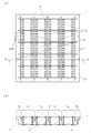
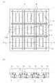
本発明の多数個取り配線基板について、添付の図面を参照しつつ説明する。図1〜図4において、1は母基板、1aは配線基板領域、1bはダミー領域、2は分割溝、2aは分割溝2の底部、3は切り欠き、3aは切り欠き3の底面、4は配線導体、5は凹部、6は穴である。 A multi-piece wiring board of the present invention will be described with reference to the accompanying drawings. 1-4, 1 is a mother board, 1a is a wiring board area, 1b is a dummy area, 2 is a dividing groove, 2a is a bottom part of the dividing
本発明の多数個取り配線基板は図1〜図4に示す例のように、中央部に複数の配線基板領域1aが縦および横の少なくとも一方の並びに配置されているとともに、複数の配線基板領域1aの周囲にダミー領域1bが配置されている母基板1と、配線基板領域1aとダミー領域1bとの境界に形成された分割溝2とを備えた多数個取り配線基板において、母基板1のダミー領域1bの一方主面から厚み方向の途中まで形成された切り欠き3を備えている。 As shown in the example shown in FIGS. 1 to 4, the multi-cavity wiring board of the present invention has a plurality of wiring board regions 1 a arranged at least in the vertical and horizontal directions at the center, and a plurality of wiring board regions. In a multi-piece wiring board including a
従って、多数個取り配線基板を撓ませて分割溝2に沿って分割したときに、切り欠き3の近傍の、ダミー領域1bに隣接して配置されていた配線基板4の、ダミー領域1b側に位置していた側面にバリが生じることを低減できる。これは、分割溝2に力を加えるときに、切り欠き3の近傍の分割溝2と分割溝2に加わる力の力点との距離が、切り欠き3の
近傍以外の分割溝2と分割溝2に加わる力の力点との距離よりも長くなることを防ぐことができるためである。Therefore, when the multi-piece wiring board is bent and divided along the dividing
また、図1〜図4に示す例のように、母基板1の他方主面の切り欠き3が形成されたダミー領域1bと配線基板領域1aとの間に形成された分割溝2の底部2aは、切り欠き3の底面3aよりも一方主面側に位置している。このような構成とすることによって、分割溝2の底部2aから切り欠き3に向かって割れることを抑制できるので、ダミー領域1b側に位置していた側面にバリが生じることを低減するのにより有効である。 1 to 4, the bottom 2a of the dividing
図1(a)に示す例においては、母基板1に縦方向に5列および横方向に4列の計20個の配線基板領域1aが配置されている。図3(a)に示す例においては、母基板1に縦方向および横方向に3列ずつの計9個の配線基板領域1aが配置されている。なお、配線基板領域1aは縦および横の少なくとも一方の並びに複数配置されていればよく、さらに多数個の並びに配置されたものであってもよい。 In the example shown in FIG. 1A, a total of 20 wiring board regions 1a in 5 rows in the vertical direction and 4 rows in the horizontal direction are arranged on the
また、配線基板領域1aは、図1に示す例のように配線基板領域1a同士が隣接するように配置されていてもよいし、図3に示す例のように、それぞれの配線基板領域1aの周囲にもダミー領域1bが配置されていても良い。それぞれの配線基板領域1aの周囲にダミー領域1bを配置する場合は、例えば、平面視で配線基板領域1aの左右または上下に、非対称な切り欠きとなる穴6を設ける場合に有効である。 Moreover, the wiring board area | region 1a may be arrange | positioned so that wiring board area | regions 1a may adjoin each other like the example shown in FIG. 1, and each wiring board area | region 1a like the example shown in FIG. A
このような配線基板領域1aの配置は、母基板1や配線基板領域1aの大きさ、配線基板領域1aに搭載される電子部品や配線導体4の配置等に合わせて設定される。 Such an arrangement of the wiring board area 1a is set in accordance with the size of the
母基板1は、例えば酸化アルミニウム質焼結体(アルミナセラミックス),ムライト質焼結体,窒化アルミニウム質焼結体,炭化珪素質焼結体,窒化珪素質焼結体,ガラスセラミックス等のセラミック材料から成る単数の絶縁層または複数の絶縁層が積層されて成るものである。この母基板1の中央部に、タングステン,モリブデン,銅,銀等の金属粉末メタライズから成る配線導体4が形成された、図1〜図4に示す配線基板領域1aが縦および横の少なくとも一方の並びに複数配置されている。 The
母基板1は、絶縁層が例えば酸化アルミニウム質焼結体から成る場合であれば、酸化アルミニウム(Al2O3),酸化珪素(SiO2),酸化マグネシウム(MgO)および酸化カルシウム(CaO)等のセラミック原料粉末に適当な有機バインダー,溶剤,可塑剤および分散剤等を添加混合して得たセラミックスラリーを従来周知のドクターブレード法等のシート成形方法を採用してシート状に成形してセラミックグリーンシートを得た後、セラミックグリーンシートに適当な打ち抜き加工を施すとともに必要に応じてこれを複数枚積層して、母基板1となる生成形体を作製して、約1500℃〜1800℃の温度で焼成することで、単数あるいは複数の絶縁層からなるものが製作される。If the
ダミー領域1bは、切り欠き3を形成するために必要な領域であるとともに、多数個取り配線基板の製造や搬送を容易とするための領域であり、このダミー領域1bを用いて母基板1となる生成形体や多数個取り配線基板の加工時や搬送時の位置決め、固定等を行なうことができる。 The
切り欠き3は、図1〜図4に示す例のように、母基板1の外縁に配置され、母基板1の下面から側面にかけて形成されている。このような切り欠き3は、多数個取り配線基板に電子部品を実装する際に、多数個取り配線基板を位置合わせするための棒状の治具が挿入される部分である。なお、切り欠き3の内面に、配線導体4と電気的に接続された電極を配置しておけば、切り欠き3の電極から電流を流して、めっき液に浸漬することによって
、電解めっきを被着できる。The
切り欠き3の底面3aと上面との間の距離L1は、0.1mm〜1mm程度であれば、分
割溝2に沿って分割するときに、平面視で切り欠き3と重なっている部分が破損しにくく、切り欠き3に位置合わせ用の治具や電解めっき用の治具を挿入できるので好ましい。If the distance L1 between the
また、切り欠き3は、図1および図3に示す例のように、分割溝2の延長線と交わらないように配置されていると、分割溝2と切り欠き3との間で不用意に割れてしまうことを抑制するのに有効である。なお、切り欠き3が、分割溝2の延長線上に配置されている場合には、分割溝2の端部が、母基板1の外縁のダミー領域1bに形成されないようにしておくことが好ましい。 If the
分割溝2は、少なくとも母基板1の各配線基板領域1aとダミー領域1bとの境界に形成されていればよいが、図1〜図4に示す例のように、母基板1の各配線基板領域1a同士の間にも形成されていてもよい。これらの分割溝2は、母基板1となる生成形体にカッター刃や金型を押し当てることによって、あるいは母基板1となる生成形体または焼成後の母基板1にレーザー加工やダイシング加工を施すことによって形成できる。分割溝2の縦断面形状は、V字状やU字状あるいは四角形状であってもよいが、図1(b),図2(b),図3(b),図4(b)に示す例のようにV字状にすると、母基板1を撓ませて分割溝2に沿って分割する際に、分割溝2の底部2aに応力が集中しやすいので、U字状または四角形状の場合に比べて小さい力で正確に分割できて好ましい。また、分割溝2は、図3(b)および図4(b)に示す例のように、母基板1の両主面に形成していても構わない。 The dividing
図1〜図4に示す例のような分割溝2が形成された母基板1は、母基板1の適当な箇所に力を加えることで一方主面側または他方主面側に凸になるように撓ませて、分割溝に沿って分割できる。また、母基板1の配線基板領域1a同士の間に分割溝2が形成されていないときには、ダイシングブレードやレーザーカッター等を用いて分割予定線で切断することによって、個々の配線基板に分割されても良い。 The
分割溝2の深さは、母基板1の材料等によって適宜設定され、例えば、母基板1の厚みの50%〜70%に形成されることが好ましい。分割溝2の深さが母基板1の厚みの50%以下であると分割しにくくなる傾向にあり、分割溝2の深さが70%以上であると運搬時の衝撃等によって分割溝2で不用意に割れやすくなる傾向がある。分割溝2の深さを上記範囲とすることで、母基板1が良好に分割されるとともに不用意に割れることのない多数個取り配線基板となる。なお、分割溝2が、母基板1の両主面に形成される場合は、両主面に形成された分割溝2の深さの合計が上記範囲に設定されていればよい。 The depth of the dividing
母基板1の他方主面の切り欠き3が形成されたダミー領域1bと配線基板領域1aとの間に形成された分割溝2の底部2aは、切り欠き3の底面3aよりも一方主面側に位置している。すなわち、図2(b)に示す例のように、分割溝2が上面に配置されている場合であれば、分割溝2は、分割溝2の底部2aと下面との距離L3が、分割溝2の底部2aと切り欠き3との距離L2よりも小さくなるような深さとしておけばよい。このような構成とすると、分割溝2の底部2aから切り欠き3の角部に向かって割れることを抑制できるので、ダミー領域1b側に位置していた側面にバリが生じることを低減するのにより有効である。 The bottom 2a of the dividing
また、図4(b)に示す例のように、分割溝2が上面および下面に、平面視で重なるように配置されている場合であれば、分割溝2の底部2a同士の間の距離L4が、分割溝2の底部2aと切り欠き3との距離L2よりも小さくなるような深さとしておくと、図2(
b)に示す例の場合と同様の理由で、分割溝2の底部2aと切り欠き3との間で割れることを抑制できるので好ましい。Further, as in the example shown in FIG. 4B, if the dividing
For the same reason as in the example shown in b), it is preferable because it can be prevented from breaking between the bottom 2a of the dividing
母基板1の分割溝2の開口幅は、例えば、0.01〜1.0mm程度であれば、母基板1を良
好に分割できるとともに、各配線基板領域1aが分割溝2の占める面積の影響で小さくならず、分割溝2の形成時に配線基板領域1aが大きく変形することがないので好ましい。分割溝2の開口幅が0.01mmよりも小さいと、母基板1を撓ませた際に、分割溝2の底部2aに加わる力が弱くなり、良好に分割できず、また、母基板1となる生成形体に分割溝2を形成し、焼成した際に、分割溝2の開口が閉じてしまったり、分割溝2の深さが浅くなってしまったりしやすくなる。また、分割溝2の開口幅が1.0mmよりも大きいと、配
線基板の一方主面または他方主面の面積が小さくなってしまう。If the opening width of the dividing
また、分割溝2の両端部が、最外周に配列される配線基板領域1aと母基板1の外周部との間のダミー領域1bに位置するように形成しておくと、母基板1の搬送時等に外部から加わる力によって母基板1が不用意に割れてしまうことを防止することができるので好ましい。 Further, if the both ends of the dividing
母基板1の上面の、各配線基板領域1a同士の境界および各配線基板領域1aとダミー領域1bとの境界には、平面視で横方向および縦方向に分割溝2が形成されている。
配線導体4は、タングステン(W),モリブデン(Mo),マンガン(Mn),銀(Ag),銅(Cu)等の金属粉末メタライズから成り、母基板1用のセラミックグリーンシートに配線導体4用のメタライズペーストをスクリーン印刷法等により所定形状に印刷して、母基板1用のセラミックグリーンシートと同時に焼成することによって、母基板1の所定位置に形成される。 The
配線導体4には、母基板1の表面や絶縁層間に配置される配線導体と、絶縁層を貫通して上下に位置する配線導体4同士を電気的に接続する貫通導体とがある。表面や絶縁層間に配置される配線導体は、母基板1用のセラミックグリーンシートにスクリーン印刷法等の印刷手段によって配線導体4用のメタライズペーストを印刷塗布し、母基板1用の生成形体とともに焼成することによって形成される。また、貫通導体は、配線導体4を形成するためのメタライズペーストの印刷塗布に先立って母基板1用のセラミックグリーンシートに金型やパンチングによる打ち抜き加工またはレーザー加工等の加工方法によって貫通導体用の貫通孔を形成し、この貫通孔に貫通導体用のメタライズペーストをスクリーン印刷法等の印刷手段によって充填しておき、母基板1となる生成形体とともに焼成することによって形成する。メタライズペーストは、主成分の金属粉末に有機バインダーおよび有機溶剤、また必要に応じて分散剤等を加えてボールミル,三本ロールミルまたはプラネタリーミキサー等の混練手段によって混合および混練することで作製する。また、セラミックグリーンシートの焼結挙動に合わせたり、焼成後の母基板1との接合強度を高めたりするために、ガラスやセラミックスの粉末を添加してもよい。貫通導体用のメタライズペーストは、有機バインダーや有機溶剤の種類や添加量によって、充填に適した、一般的に配線導体4用のメタライズペーストよりも高い粘度に調整される。なお、メタライズペーストには母基板1との接合強度を高めるために、ガラスやセラミックスを含んでいても構わない。 The
なお、配線導体4の露出する表面には、ニッケル,金等の耐蝕性に優れる金属めっきが被着され、接続電極または外部端子電極となる。これによって、配線導体4が腐食することを効果的に抑制することができるとともに、配線導体4と電子部品との接合、配線導体4とボンディングワイヤとの接合、および配線導体4と外部回路基板の配線導体との接合を強固にすることができる。また、例えば、配線導体4の露出する表面には、厚さ1〜10
μm程度のニッケルめっき層と厚さ0.1〜3μm程度の金めっき層とが、電解めっき法も
しくは無電解めっき法により順次被着される。The exposed surface of the
A nickel plating layer having a thickness of about μm and a gold plating layer having a thickness of about 0.1 to 3 μm are sequentially deposited by an electrolytic plating method or an electroless plating method.
母基板1の一方主面に凹部5が形成され、分割溝2が他方主面側に開口している場合には、分割溝2の底部2aは、分割溝2の底部2aと凹部5の底面との距離よりも、分割溝2の底部2aと他方主面との距離が短くなるように配置されていることが好ましい。また、両主面に対向するように分割溝2が形成されている場合には、分割溝2の底部2a同士の距離は、それぞれの分割溝2と凹部5の底面との距離よりも短いことが好ましい。このような構成とすることによって、分割溝2の底部2aと凹部5の底面の角部との間で分割されてしまうことを抑制するのに有効である。 When the concave portion 5 is formed on one main surface of the
図3に示す例のように、配線基板領域1aとダミー領域1bとにまたがって、穴6が配置されていてもよい。穴6は、母基板1の少なくとも一方の主面に開口して形成されている。このような穴6は、多数個取り配線基板を分割して配線基板とした際に、キャスタレーション用の切り欠きや、配線基板を位置合わせするための切り欠きとなる。このような穴6は、母基板1の厚み方向の途中まで形成された底のある穴や、母基板1を厚み方向に貫通した貫通孔であり、平面視で、矩形状や六角形状等の多角形状または円形や楕円形状の円形状等に形成される。 As in the example illustrated in FIG. 3, the
このような穴6は、母基板1を分割する際に、分割された母基板1の外縁のダミー領域1bに形成された切り欠きとなる。このようなときには、穴6が形成されたダミー領域1bと配線基板領域1aとの間に形成された分割溝2の底部2aは、穴6の底面よりも下側に位置していることが好ましい。このような構成とすることによって、母基板1を分割する際に、分割溝2の底部2aから穴6が分割された切り欠きに向かって割れることを抑制できるので、ダミー領域1b側に位置していた側面にバリが生じることを低減するのにより有効である。なお、配線基板の側面に厚み方向に貫通した切り欠きを形成する場合には、穴6はダミー領域1b側では母基板1の厚み方向の途中まで形成され、配線基板領域1a側では貫通するように形成されていてよい。 Such a
上記の穴6を有する母基板1は、金型で打ち抜くことやレーザー加工することによって、所望の位置に穴6用の第1の貫通孔を形成したセラミックグリーンシートを積層して焼成したり、第1の貫通孔を形成した第1のセラミックグリーンシートを、第2のセラミックグリーンシート上に積層して焼成することで作製できる。また、穴6を有する母基板1は、セラミックグリーンシートを焼成したセラミック焼結体に、ドリル等の機械加工や、貫通孔を形成する場合に比べて出力を落としたレーザー加工を行なっても作製できる。 The
穴6をキャスタレーション用の切り欠きとする場合であれば、穴6は、内面に配線導体4が被着されており、母基板1を分割した際には、穴6が分割されることによって、配線基板の側面に端子電極が被着された切り欠きを形成して、いわゆるキャスタレーション導体となる。このような配線導体4は、上記のメタライズペーストを用いて、穴6となる母基板1用のセラミックグリーンシートの穴の内面に、スクリーン印刷法等の印刷手段によって印刷塗布し、母基板1用の生成形体とともに焼成することによって形成する。なお、メタライズペーストは、穴6の寸法等に応じて、有機溶剤等の添加量を調整することで適当な粘度にして用いられる。 If the
電子部品の搭載は、例えば、電子部品がフリップチップ型の半導体素子である場合には、はんだバンプや金バンプ、または導電性樹脂(異方性導電樹脂等)等の接合材を介して、半導体素子の電極と配線導体4とを電気的および機械的に接続することによって行なわれる。また、接合材によって電子部品を電子部品搭載領域に接合した後に、電子部品と配線基板との間にアンダーフィルを注入してもよい。あるいは、例えば、電子部品がワイヤ
ボンディング型の半導体素子である場合には、電子部品を接合材によって電子部品搭載領域に固定した後、ボンディングワイヤを介して半導体素子の電極と配線導体4とを電気的に接続する。また、例えば、電子部品が水晶振動子等の圧電素子である場合には、導電性樹脂等の接合材によって圧電素子の固定と圧電素子の電極と配線導体4との電気的な接続を行なう。また、必要に応じて、電子部品の周囲に抵抗素子や容量素子等の第2の電子部品を搭載してもよい。For example, when the electronic component is a flip chip type semiconductor element, the electronic component is mounted on the semiconductor via a bonding material such as a solder bump, a gold bump, or a conductive resin (anisotropic conductive resin, etc.). This is performed by electrically and mechanically connecting the electrode of the element and the
なお、本発明は上述の実施の形態の例に限定されるものではなく、本発明の要旨を逸脱しない範囲であれば種々の変更は可能である。例えば、図3に示す例の多数個取り配線基板において、穴6のダミー領域1bに形成された部分に貫通孔が形成されていると、穴6内に入っためっき液が留まりにくいので好ましい。また、例えば、凹部5は母基板1の両主面に形成されていても構わない。 Note that the present invention is not limited to the above-described embodiments, and various modifications can be made without departing from the scope of the present invention. For example, in the multi-cavity wiring board of the example shown in FIG. 3, it is preferable that the through hole is formed in the portion formed in the
1・・・・母基板
1a・・・配線基板領域
1b・・・ダミー領域
2・・・・分割溝
2a・・・分割溝2の底部
3・・・・切り欠き
3a・・・切り欠き3の底面
4・・・・配線導体
5・・・・凹部
6・・・・穴DESCRIPTION OF
Claims (2)
Translated fromJapanesePriority Applications (1)
| Application Number | Priority Date | Filing Date | Title |
|---|---|---|---|
| JP2011015432AJP5697467B2 (en) | 2011-01-27 | 2011-01-27 | Multiple wiring board |
Applications Claiming Priority (1)
| Application Number | Priority Date | Filing Date | Title |
|---|---|---|---|
| JP2011015432AJP5697467B2 (en) | 2011-01-27 | 2011-01-27 | Multiple wiring board |
Publications (2)
| Publication Number | Publication Date |
|---|---|
| JP2012156382Atrue JP2012156382A (en) | 2012-08-16 |
| JP5697467B2 JP5697467B2 (en) | 2015-04-08 |
Family
ID=46837781
Family Applications (1)
| Application Number | Title | Priority Date | Filing Date |
|---|---|---|---|
| JP2011015432AActiveJP5697467B2 (en) | 2011-01-27 | 2011-01-27 | Multiple wiring board |
Country Status (1)
| Country | Link |
|---|---|
| JP (1) | JP5697467B2 (en) |
Cited By (3)
| Publication number | Priority date | Publication date | Assignee | Title |
|---|---|---|---|---|
| JP2014063892A (en)* | 2012-09-21 | 2014-04-10 | Kyocera Corp | Multiple patterning wiring board |
| US8952269B2 (en) | 2011-05-19 | 2015-02-10 | Ngk Spark Plug Co., Ltd. | Wiring substrate, multi-piece wiring substrate array, and manufacturing method therefor |
| JP2017037915A (en)* | 2015-08-07 | 2017-02-16 | 京セラ株式会社 | Multi-cavity wiring board and wiring board |
Citations (3)
| Publication number | Priority date | Publication date | Assignee | Title |
|---|---|---|---|---|
| JP2008010560A (en)* | 2006-06-28 | 2008-01-17 | Kyocera Corp | Wiring board, multi-cavity wiring board, electronic component storage package and electronic device |
| JP2010080567A (en)* | 2008-09-25 | 2010-04-08 | Kyocera Corp | Multi-piece substrate, wiring board, and electronic apparatus |
| JP2010153423A (en)* | 2008-12-24 | 2010-07-08 | Kyocera Corp | Multiple patterning wiring substrate and wiring substrate, and electronic device |
- 2011
- 2011-01-27JPJP2011015432Apatent/JP5697467B2/enactiveActive
Patent Citations (3)
| Publication number | Priority date | Publication date | Assignee | Title |
|---|---|---|---|---|
| JP2008010560A (en)* | 2006-06-28 | 2008-01-17 | Kyocera Corp | Wiring board, multi-cavity wiring board, electronic component storage package and electronic device |
| JP2010080567A (en)* | 2008-09-25 | 2010-04-08 | Kyocera Corp | Multi-piece substrate, wiring board, and electronic apparatus |
| JP2010153423A (en)* | 2008-12-24 | 2010-07-08 | Kyocera Corp | Multiple patterning wiring substrate and wiring substrate, and electronic device |
Cited By (3)
| Publication number | Priority date | Publication date | Assignee | Title |
|---|---|---|---|---|
| US8952269B2 (en) | 2011-05-19 | 2015-02-10 | Ngk Spark Plug Co., Ltd. | Wiring substrate, multi-piece wiring substrate array, and manufacturing method therefor |
| JP2014063892A (en)* | 2012-09-21 | 2014-04-10 | Kyocera Corp | Multiple patterning wiring board |
| JP2017037915A (en)* | 2015-08-07 | 2017-02-16 | 京セラ株式会社 | Multi-cavity wiring board and wiring board |
Also Published As
| Publication number | Publication date |
|---|---|
| JP5697467B2 (en) | 2015-04-08 |
Similar Documents
| Publication | Publication Date | Title |
|---|---|---|
| JP5731404B2 (en) | Multi-cavity wiring board, wiring board and electronic device | |
| JP5052398B2 (en) | Multi-cavity wiring board, wiring board and electronic device | |
| JP5697467B2 (en) | Multiple wiring board | |
| CN103081574B (en) | Circuit board and electronic installation | |
| JP4721926B2 (en) | Multiple wiring board | |
| JP5247415B2 (en) | Multi-cavity wiring board, wiring board and electronic device | |
| JP5855822B2 (en) | Multiple wiring board | |
| JP5743779B2 (en) | Multi-circuit board and electronic device | |
| JP5956185B2 (en) | Multiple wiring board | |
| JP5818654B2 (en) | Multi-cavity wiring board, wiring board and electronic device | |
| JP4812516B2 (en) | Multiple wiring board | |
| JP5460002B2 (en) | Multi-cavity wiring board, wiring board and electronic device | |
| JP2017063093A (en) | Wiring board, electronic device and electronic module | |
| JP5574848B2 (en) | Multiple wiring board | |
| JP2008091560A (en) | WIRING BOARD, MULTILAYER WIRING BOARD, ELECTRONIC DEVICE, AND MANUFACTURING METHOD THEREOF | |
| JP4646825B2 (en) | Multiple wiring board | |
| JP5679827B2 (en) | Wiring board and multi-cavity wiring board | |
| JP2005136172A (en) | Multiple wiring board | |
| JP5791450B2 (en) | Multi-cavity wiring board and wiring board | |
| JP6130278B2 (en) | Multi-wiring board | |
| JP2008211017A (en) | Manufacturing method of mother board with base, electronic component mounting mother board, and electronic apparatus | |
| JP2015141933A (en) | Wiring board and electronic device |
Legal Events
| Date | Code | Title | Description |
|---|---|---|---|
| A621 | Written request for application examination | Free format text:JAPANESE INTERMEDIATE CODE: A621 Effective date:20131216 | |
| A977 | Report on retrieval | Free format text:JAPANESE INTERMEDIATE CODE: A971007 Effective date:20140926 | |
| A131 | Notification of reasons for refusal | Free format text:JAPANESE INTERMEDIATE CODE: A131 Effective date:20140930 | |
| A521 | Written amendment | Free format text:JAPANESE INTERMEDIATE CODE: A523 Effective date:20141126 | |
| TRDD | Decision of grant or rejection written | ||
| A01 | Written decision to grant a patent or to grant a registration (utility model) | Free format text:JAPANESE INTERMEDIATE CODE: A01 Effective date:20150113 | |
| A61 | First payment of annual fees (during grant procedure) | Free format text:JAPANESE INTERMEDIATE CODE: A61 Effective date:20150210 | |
| R150 | Certificate of patent or registration of utility model | Ref document number:5697467 Country of ref document:JP Free format text:JAPANESE INTERMEDIATE CODE: R150 |