JP2012156162A - Light emitting device, manufacturing method of the light emitting device, and lighting device - Google Patents
Light emitting device, manufacturing method of the light emitting device, and lighting deviceDownload PDFInfo
- Publication number
- JP2012156162A JP2012156162AJP2011011306AJP2011011306AJP2012156162AJP 2012156162 AJP2012156162 AJP 2012156162AJP 2011011306 AJP2011011306 AJP 2011011306AJP 2011011306 AJP2011011306 AJP 2011011306AJP 2012156162 AJP2012156162 AJP 2012156162A
- Authority
- JP
- Japan
- Prior art keywords
- light
- emitting device
- resin layer
- substrate
- convex
- Prior art date
- Legal status (The legal status is an assumption and is not a legal conclusion. Google has not performed a legal analysis and makes no representation as to the accuracy of the status listed.)
- Granted
Links
Images


Landscapes
- Led Device Packages (AREA)
Abstract
Description
Translated fromJapanese本発明は、LED素子を用いた発光装置に係り、特にその色むらを改善した発光装置に関する。 The present invention relates to a light emitting device using an LED element, and more particularly to a light emitting device with improved color unevenness.
LED素子を用いた発光装置では、所望の発光色例えば白色の発光を得るために、LED素子と蛍光体等の波長変換材料とを組み合わせた発光装置が多用されている。波長変換材料は、通常、LED素子の封止樹脂中に分散させて、LED素子を覆うように設けられる。従来、LED素子を搭載する基板上に、凹部(ホーン)を形成し、その底部にLEDを搭載するとともに凹部内に蛍光体含有樹脂を充填することにより、発光装置を製造している。 In light emitting devices using LED elements, in order to obtain a desired light emission color, for example, white light emission, a light emitting device in which an LED element and a wavelength conversion material such as a phosphor are combined is frequently used. The wavelength conversion material is usually provided so as to cover the LED element by being dispersed in the sealing resin of the LED element. Conventionally, a light emitting device is manufactured by forming a recess (horn) on a substrate on which an LED element is mounted, mounting an LED on the bottom thereof, and filling the recess with a phosphor-containing resin.
しかし、この発光装置では、LED素子から発する光が蛍光体層を通過するときの光路長が、LED素子の直上と周囲で異なるために、色むらが発生するという問題がある。例えば、青色LEDと蛍光体とを組み合わせた発光装置の場合、LED素子の直上では青色となり、周囲が蛍光体色である黄色になる。 However, in this light emitting device, there is a problem that uneven color occurs because the light path length when the light emitted from the LED element passes through the phosphor layer is different between directly above and around the LED element. For example, in the case of a light emitting device in which a blue LED and a phosphor are combined, the light is blue immediately above the LED element and the surrounding is yellow, which is a phosphor color.
これに対し、金型とLED素子との間に蛍光体含有樹脂を注入して硬化させることにより、LED素子上に蛍光体層を半球状に設ける方法がある(特許文献1〜3)。樹脂の成型には、コンプレッションモールド法が広く用いられている。蛍光体層を半球状にすることにより、光路長差に起因する色むら発生の問題は軽減されるが、十分ではない。また、コンプレッションモールド法では、蛍光体含有樹脂に含まれる気泡を除去するために、金型とLED素子を搭載した基板との間に、薄い離型性のシートを挟みこんで真空引きを行う必要がある。このため、基板とシートとの間に蛍光体含有樹脂の薄い層が形成され、その状態で蛍光体層の成型が行われ、基板のLED搭載面に薄い樹脂層が形成される。 On the other hand, there is a method of providing a phosphor layer in a hemispherical shape on an LED element by injecting and curing a phosphor-containing resin between a mold and the LED element (Patent Documents 1 to 3). The compression molding method is widely used for resin molding. By making the phosphor layer hemispherical, the problem of color unevenness due to the optical path length difference is reduced, but it is not sufficient. In addition, in the compression molding method, in order to remove bubbles contained in the phosphor-containing resin, it is necessary to evacuate by placing a thin releasable sheet between the mold and the substrate on which the LED element is mounted. There is. For this reason, a thin layer of phosphor-containing resin is formed between the substrate and the sheet, and the phosphor layer is molded in that state, and a thin resin layer is formed on the LED mounting surface of the substrate.
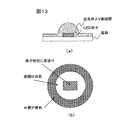
コンプレッションモールド法により製造した発光装置では、半球状の樹脂層の他に、その周囲に形成された薄い樹脂層においても、それに含まれる蛍光体がLED素子により発光することになり、周囲が半球状の部分よりも黄色くなる色むらを生じる。LED素子を用いた光源は、レンズ等の集光光学部品と組み合わせて照明装置等として用いられることが多いが、色むらがある光源の光をそれら集光光学部品で投影すると色分離され、均一な照明が得られない。図13に、コンプレッションモールド法により製造した白色LED発光装置(光源)の断面図(a)と、投影光の色分離の様子(b)を示す。図示するように、LED素子の直上に相当する領域は、素子形状に青抜けと呼ばれる青い領域が発生し、また半球状の蛍光体層の外周に相当する領域は黄色くなる。 In the light emitting device manufactured by the compression molding method, in addition to the hemispherical resin layer, even in a thin resin layer formed around it, the phosphor contained therein emits light by the LED element, and the periphery is hemispherical. The color unevenness which becomes yellow rather than the part of is produced. Light sources using LED elements are often used as illumination devices in combination with condensing optical components such as lenses, but when light from unevenly colored light sources is projected by these condensing optical components, the colors are separated and uniform Can't get enough lighting. FIG. 13 shows a cross-sectional view (a) of a white LED light emitting device (light source) manufactured by the compression molding method and a state (b) of color separation of projection light. As shown in the drawing, in the region corresponding to the area directly above the LED element, a blue region called blue void is generated in the element shape, and the region corresponding to the outer periphery of the hemispherical phosphor layer is yellow.
本発明は、LED素子を覆う凸状の樹脂層が形成された発光装置における上記色むら発生の問題を解決し、色むらがなく均一な発光色を実現できる発光装置を提供することを課題とする。 An object of the present invention is to solve the above-described problem of uneven color generation in a light emitting device in which a convex resin layer covering an LED element is formed, and to provide a light emitting device capable of realizing a uniform emission color without color unevenness. To do.
上記課題を解決するため、本発明は、凸状の樹脂層の周囲の薄膜状の樹脂層からの発光を積極的に利用し、薄膜状樹脂層からの光と、LED素子直上からの光との混色によって色むらをなくし、均一な発光を実現する。 In order to solve the above-described problems, the present invention actively utilizes light emitted from a thin resin layer around a convex resin layer, and the light from the thin resin layer and the light directly above the LED element The color mixture eliminates uneven color and realizes uniform light emission.
即ち、本発明の発光装置の主な態様は、以下のような構成を備える。
基板と、前記基板上に搭載されたLED素子と、前記基板上に形成され、前記LED素子を覆う波長変換材料含有樹脂層とを備えた発光装置であって、前記樹脂層は、前記LEDを覆う凸部とそれに続く平坦な薄膜部とを有し、前記凸部周囲の前記薄膜部の上に反射部が形成されている。That is, the main aspect of the light-emitting device of the present invention has the following configuration.
A light emitting device comprising a substrate, an LED element mounted on the substrate, and a wavelength conversion material-containing resin layer formed on the substrate and covering the LED element, wherein the resin layer includes the LED A reflective part is formed on the thin film part around the convex part.
或いは、基板と、前記基板上に搭載された、複数のLED素子の配列と、前記基板上に形成され、前記複数のLED素子の配列を覆う波長変換材料含有樹脂層とを備えた発光装置であって、前記樹脂層の、前記複数のLED素子の間の領域の上に反射部が形成されている。 Alternatively, a light-emitting device including a substrate, an array of a plurality of LED elements mounted on the substrate, and a wavelength conversion material-containing resin layer formed on the substrate and covering the array of the plurality of LED elements. And the reflection part is formed on the area | region between these LED elements of the said resin layer.
また、本発明は、上記本発明の発光装置を製造する方法を提供する。即ち、本発明の発光装置の製造方法は、基板上に、1ないし複数のLED素子を搭載する工程と、前記基板上に、コンプレッションモールド法により、前記LED素子を覆う凸形状の樹脂層を形成する工程と、前記凸形状の樹脂層の周囲に、反射部を形成する工程とを含む。 The present invention also provides a method for producing the light emitting device of the present invention. That is, in the method for manufacturing a light emitting device of the present invention, a step of mounting one or a plurality of LED elements on a substrate, and a convex resin layer covering the LED elements are formed on the substrate by a compression molding method. And a step of forming a reflection portion around the convex resin layer.
或いは、基板上に、1ないし複数のLED素子を搭載する工程と、前記基板上に、コンプレッションモールド法により、前記LED素子を覆う凸形状の樹脂層を形成する工程と、拡散材含有樹脂を用いて、前記樹脂層を覆う拡散部を形成する工程と、前記拡散部の、前記凸形状の樹脂層周囲の領域の上に、反射部を形成する工程を含む。 Alternatively, a step of mounting one or more LED elements on a substrate, a step of forming a convex resin layer covering the LED elements by a compression molding method on the substrate, and a diffusing material-containing resin are used. A step of forming a diffusion portion covering the resin layer, and a step of forming a reflection portion on a region around the convex resin layer of the diffusion portion.
本発明によれば、樹脂層の凸部の周囲にある薄膜部の上に、反射部を設けることにより、薄膜部から発生する光が、直接、外部に出射されることを防止するとともに、薄膜部と反射部との界面で反射させて、凸部側に戻すことができる。これにより、凸部周囲の発光に起因する色むらを抑制すると共に、凸部周囲からの発光とLED素子直上に向かう光との混色により、LED素子直上の光に起因する色むらを緩和し、全体として均一な発光を実現することができる。 According to the present invention, by providing the reflective portion on the thin film portion around the convex portion of the resin layer, the light generated from the thin film portion is prevented from being directly emitted to the outside, and the thin film portion It can be reflected at the interface between the part and the reflecting part and returned to the convex part side. As a result, color unevenness caused by light emission around the convex portion is suppressed, and color unevenness caused by light directly above the LED element is mitigated by color mixture of light emission from the periphery of the convex portion and light directed directly above the LED element, Uniform light emission can be realized as a whole.
以下、本発明の発光装置の実施の形態を、図面を参照して説明する。 Embodiments of a light emitting device according to the present invention will be described below with reference to the drawings.
<第一の実施形態>
図1に本実施形態の発光装置の一例を示す。図1(a)は、発光装置を上から見た図、(b)は、(a)のA-A断面図である。<First embodiment>
FIG. 1 shows an example of the light emitting device of this embodiment. 1A is a view of the light emitting device as viewed from above, and FIG. 1B is a cross-sectional view taken along line AA of FIG.
図示するように、本実施形態の発光装置10は、基板11と、LED素子12と、樹脂層13と、反射部14とから構成されている。 As shown in the drawing, the
基板11は、Al2O3、AlNなどのセラミック、ガラスエポキシ、或いはCu、Alなどの金属材料からなる板状部材である。厚みは、限定されるものではないが、通常0.4〜1mm程度である。基板11のLED素子搭載面或いはその裏面には、図示しないが、LED素子12と外部電源との電気接続を図るための電極が形成されている。また基板11が金属材料からなる場合には、正極と負極とを絶縁するためのスリットや絶縁部が形成されている。The
LED素子12には、2つの電極端子部が上面に形成されたフェイスアップ素子、下面に形成されたフリップ素子、MB(メタルボンド)素子等があり、そのいずれを使用してもよい。LED素子のサイズも特に限定されず、縦×横が0.5mm×0.3mm程度、厚み0.12mm程度の比較的小さい素子から、一辺が1mm以上の大きな素子まで使用できる。 The
樹脂層13は、樹脂と蛍光体等の波長変換材料と、必要に応じてフィラー等の添加剤を含む。樹脂としては、コンプレッションモールド法に適した樹脂であれば特に限定されず、シリコーン樹脂、エポキシとシリコーンとのハイブリッド樹脂、エポキシ樹脂、ウレタン樹脂などが使用できる。信頼性の面からシリコーン樹脂が最適である。また高輝度を得るためには、屈折率が高い樹脂を使用することが好ましいが、一般に高屈折率樹脂は光による劣化が早いため、高信頼性が要求される用途では、低屈折率樹脂を用いることが好ましい。樹脂の屈折率は、樹脂の種類の選択や添加するフィラーの含有量により調節することができる。 The
波長変換材料は、LED素子が発する光を吸収して、吸収した光と異なる波長の光を発する材料であり、LEDの発光及び所望の発光色に応じて、窒化系或いは酸窒化物系蛍光体、YAG系蛍光体、BAM蛍光体(アルミン酸系青色蛍光体)、SiAlON蛍光体等の蛍光体を適宜選択する。例えば、黄色発光蛍光体として、Y3Al5O12:Ce3+、緑色発光蛍光体として、Y3(Al,Ga)5O12:Ce3+、赤色発光蛍光体として、CaAlSiN3:Euなどを使用することができる。The wavelength conversion material is a material that absorbs light emitted from the LED element and emits light having a wavelength different from the absorbed light, and is a nitride or oxynitride phosphor depending on the light emission and desired emission color of the LED , YAG phosphor, BAM phosphor (aluminate blue phosphor), SiAlON phosphor and the like are appropriately selected. For example, Y3 Al5 O12 : Ce3+ as a yellow light emitting phosphor, Y3 (Al, Ga)5 O12 : Ce3+ as a green light emitting phosphor, and CaAlSiN3 : Eu as a red light emitting phosphor. Etc. can be used.
フィラーは、製造工程における封止樹脂の粘度を調整するためや、色むらを軽減するための拡散材として用いられる。蛍光体およびフィラーの含有量は特に限定されないが、樹脂に対する蛍光体およびフィラーの合計含有量の重量割合で、好ましくは5〜80重量%、より好ましくは10〜40重量%である。 The filler is used as a diffusing material for adjusting the viscosity of the sealing resin in the manufacturing process or for reducing color unevenness. The content of the phosphor and the filler is not particularly limited, but is preferably 5 to 80% by weight, more preferably 10 to 40% by weight, based on the weight ratio of the total content of the phosphor and the filler with respect to the resin.
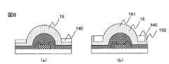
樹脂層13の形状は、LED素子13を覆う部分がほぼ半球状の凸部131であり、その周囲は基板11の表面と平行な薄膜部133になっている。半球状の凸部131のサイズは、LED素子13のサイズによって異なるが、図2に示すように、LED素子13の幅をDとすると、LED素子上面と平行な方向の幅Wが、D+2×0.6(mm)程度、LED素子上面からの高さHが、W/2程度である。前掲の幅0.5mm、厚み0.12mmのLED素子の場合、凸部131の形状は、ほぼ半径1.7mmの半球状となる。このような形状とすることによりLED素子の出射面である上面から凸部131表面までの光路長をほぼ均一とすることができる。一方、薄膜部133の厚みTは、好ましくはLED素子13の厚み以下、より好ましくは0.1mm以下である。薄膜部133の厚みがLED素子の厚みを超えると、凸部131を半球状にした効果即ち光路長の均一化が阻害される。 As for the shape of the
反射部14は、樹脂層13との界面において、樹脂層13から発する光を反射するとともに、樹脂層13から外に出射する光を遮蔽する機能を持つ。このような機能を持つ反射材料として、光を正反射する金属や鏡面加工された部材を用いることも可能であるが、拡散反射する材料、具体的には白色反射材料からなることが好ましい。拡散反射する材料を用いることにより、樹脂層13の薄膜部133から発生する光を拡散して凸部131に向けることができ、凸部131においてLED素子13の直上に向かう光との混色を効率よく行うことができる。また反射部14の製造も容易となる。拡散反射する材料として、具体的には、TiO2、Al2O3、AlN、SiO2、ZnOなどの白色フィラーを、シリコーン樹脂、エポキシとシリコーンとのハイブリッド樹脂、エポキシ樹脂、ウレタン樹脂などの樹脂に混合した白色樹脂を用いることができる。反射部14を塗布によって形成する場合には、塗布が容易で且つ層形成後の形状安定が良好な、チクソ性を向上させた樹脂を選定することが好ましい。また反射部14を接着等によって形成する場合には、Al2O3等のセラミック材や、TiO2などの白色フィラー含有プラスチック材を加工した白色反射板を用いることもできる。The reflecting
反射部14は、上述した樹脂層13の薄膜部133上であって、凸部131の外側の領域に形成される。厚みt1は、好ましくは0.2mm以上、より好ましくは0.5mm以上とする。厚みt1を0.2mm以上とすることにより、その下にある樹脂層13からの光をほぼ遮蔽することができる。反射部14は、薄膜部133の全面に設けることが理想的であるが、凸部131の外周からの幅d1が0.2mm以上であればよく、好ましくは0.5mm以上とする。外周からの幅d1を0.2mm以上とすることにより、色むらの原因となる蛍光体含有樹脂層13からの光に対し十分な遮光性を得ることができるとともに、樹脂層13からの光を樹脂層13側に反射させて、LED素子13からの光と混合させることができる。 The
なお反射部14は、必ずしも、凸部131の外周と密着している必要はなく、図2の部分拡大図に示すように、反射部14の側面と凸部131の外周面との間に隙間18があってもよい。隙間18に露出する樹脂層13(薄膜部133)から発する光は、一部が反射部14の側面で反射されて樹脂層13(凸部131)に入射し、一部は樹脂層13の凸部131から出射される光と混じって混色されるため、目立った色むらを引き起こさないからである。許容できる隙間18の間隔は、樹脂層(凸部131)の厚みや反射部14の厚みによって異なるが、0.25mm以下であることが好ましい。 Note that the reflecting
本実施の形態において、色むらを発生しない原理を、図3(a)を参照して説明する。図3(a)において、樹脂層13の薄膜部133で発生する光(周囲黄色発光)の軌跡を点線で、LED素子12から直上に向かう光(所謂青抜け発光)の軌跡を一点鎖線で示す。図示するように、本実施形態の発光装置では、LED素子12の上面から各方向に拡散して発生する光は、ほぼ凸部131の表面までの光路長が等しいため、同じ色味の光(例えば白色光)となって出射されるが、LED素子12の上面中心部では発光の輝度が最も高くなるため、直上ではLED素子自体の発光色、例えば青色が優勢となる。一方、LED素子の側面からの発光により、薄膜部133からも発光するが、この領域では蛍光体の色例えば黄色が優勢な発光となる。この薄膜部133からの発光は、その上部に反射部14が形成されているため、直接外側に出射されることなく、反射部14との界面で反射されて凸部133の中心側に向かう。この黄色が優勢な光と、LED素子12から直上に向かう、青色が優勢な光が混じり、混色され、凸部133からは白色の発光が得られる。即ち、LED素子12の青抜け発光と、周辺の黄色発光とが抑制され、色むらのない発光が得られる。 In the present embodiment, the principle that color unevenness does not occur will be described with reference to FIG. In FIG. 3A, the locus of light (ambient yellow light emission) generated in the
次に本実施形態の発光装置の製造方法を説明する。図4に製造方法の一例を示す。
まずパッケージ基板11の上に、ダイボンディンング、ワイヤボンディング等の方法により、LED素子12を固定すると共に電気的に接続する(a)。次に、LED素子12を実装した基板11と、金型40との間に、樹脂層形成用樹脂を注入し、コンプレッションモールドにて樹脂層13を形成する(b)。コンプレッションモールドでは、金型40と樹脂との間にフッソ系樹脂シートのような離型シート(図示せず)を介在させて成形と同時に樹脂を真空引きし、樹脂内の気泡を除去する。これにより、LED素子12を覆う凸部131とその周辺に広がる薄膜部133とからなる樹脂層13が形成される。次いで、白色フィラー含有樹脂塗布液をディスペンサー41で凸部131の周囲に塗布し、白色フィラー含有樹脂を硬化させて、反射部14を形成する(c)。Next, a method for manufacturing the light emitting device of this embodiment will be described. FIG. 4 shows an example of the manufacturing method.
First, the
ステップ(c)で、白色フィラー含有樹脂塗布液を塗布・硬化させて反射部14を作成する代わりに、中央に凸部13の外周の径とほぼ同じ内径の開口を持つ白色反射板を用意し、これをシリコーン系接着剤等の接着剤で接着するとともに加圧手段42で押圧し、反射部14を形成することも可能である(d)。 Instead of applying and curing the white filler-containing resin coating solution in step (c) to prepare the reflecting
本実施形態によれば、LED素子12を覆う半球状の樹脂層凸部131の周辺に、凸部周辺の薄膜部133を覆う反射部14を設けたことにより、色むらの解消された発光装置を得ることができる。 According to the present embodiment, the light emitting device in which the color unevenness is eliminated by providing the reflecting
<第二の実施形態>
図5に本実施形態の発光装置の一例を示す。図5(a)は、発光装置を上から見た図、(b)は、(a)のB-B断面図である。図1と同じ要素は、同じ符号で示す。
図示するように、本実施形態の発光装置10は、基板11と、LED素子12と、樹脂層13と、反射部140と、拡散層15とから構成されている。<Second Embodiment>
FIG. 5 shows an example of the light emitting device of this embodiment. 5A is a view of the light emitting device as viewed from above, and FIG. 5B is a cross-sectional view taken along the line BB in FIG. The same elements as those in FIG. 1 are denoted by the same reference numerals.
As shown in the figure, the
基板11、LED素子12及び樹脂層13の構成は、第一の実施形態と同様であり、説明を省略し、異なる点を中心に説明する。 The configurations of the
反射部140を構成する材料は、第一の実施形態と同様であるが、本実施形態では図5(b)の断面図に示す樹脂層の凸部131と反射部140との間に、拡散層15が設けられるため、反射部140の位置やサイズの条件が第一実施形態とは異なる。反射部140は、凸部131との間に拡散層15を受け入れる封止部として機能するように、凸部131の外周の径より大きな内径の開口を持つリング状部材とする。リングの高さhは、凸部131の高さの半分程度、凸部131の外径と反射部140開口の内径との差d2(すなわち拡散層13の側部の厚み)は、好ましくは0.25mm以下である。一例として、半球状凸部131の高さが0.75mmであるとすると、反射部140の高さhは0.375mm以上であればよい。反射部140の高さhと、その開口の内径(距離d2+凸部131の半径)を上述した範囲とすることにより、反射部140形成後に拡散層15を構成する材料を、反射部140で囲まれる空間に注入したときに、凸部131を覆う半球状の拡散層14を形成することができる。またまた反射部140と凸部131との間に位置する樹脂層の薄膜部133からの発光による色むらを目立たなくすることができる。反射部140(リング)の厚みt2は、好ましくは0.2mm以上とする。これにより、色むらの原因となる薄膜部133からの発光のほとんどを、反射部140との界面で反射し、凸部131側へ向けることができる。 The material constituting the
反射部140は、第一の実施形態と同様に、塗布によって形成することも可能であるが、セラミック材或いは白色フィラー含有プラスチック材からなるリング状部材を用意し、これを接着剤で樹脂層の薄膜部133に接着してもよい。 The
拡散層15は、光拡散剤と樹脂と、必要に応じて加えられる添加剤とからなる。光拡散剤としては、TiO2、Al2O3、AlN、SiO2、ZnOなどのフィラーを用いることができる。樹脂としては、シリコーン樹脂、エポキシとシリコーンとのハイブリッド樹脂、エポキシ樹脂、ウレタン樹脂を用いることができ、特に信頼性の面からシリコーン樹脂が好適である。フィラーの含有量は、光拡散性と光透過性を両立するために、樹脂に対し、好ましくは0.5〜20重量%、より好ましくは0.5〜10重量%である。The
本実施の形態において、色むらを発生しない原理を、図3(b)を参照して説明する。図3(b)においても、図3(a)と同様に、樹脂層13の薄膜部133から黄色が優勢な発光を生じる。そのうち、樹脂層13の内部を伝播する光は、図3(a)と同様であるので、ここでは省略し、樹脂層13から拡散部15に出射する光を点線で示している。図3(a)の場合と異なり、凸部131と反射部140との間に位置する薄膜部133は、反射部140で覆われていないため、そこから出た黄色が優勢な光は拡散部15に入射する。ここで光拡散材によって拡散され、そのうち多くの光は直接或いは反射部140の側面で反射されて、凸部133の中心側に向かい、LED素子12からの光と混色される。また一部は凸部131に入射し、ここでLED素子12からの光と混色される。従って、拡散部15がない状態では、LED素子直上と薄膜部133直上では色味の分布があったとしても、その分布は拡散部15によって平準化され、発光装置全体として均一な色味の発光が得られる。なお、図3(b)で図示を省略した、薄膜部133から出て反射部140との界面で反射される光が、色むらをさらに解消するのに寄与することは、図3(a)の場合と同様である。 In the present embodiment, the principle that color unevenness does not occur will be described with reference to FIG. In FIG. 3B as well, similarly to FIG. 3A, yellow emits light predominantly from the
次に本実施形態の発光装置の製造方法を説明する。図6に製造方法の一例を示す。
本実施形態においても、基板にLED素子を実装する工程(a)、その上にコンプレッションモールドにより樹脂層を形成する工程(b)、および反射部140を形成する工程(c)又は(d)は、図4に示す第一の実施形態の発光装置の製造方法と同様である。但し、工程(c)又は(d)において、反射部140は、樹脂層13の凸部131外周から所定の間隔を持ち、且つその高さが凸部131の半分以上となるように形成される。しかる後に、反射部140によって閉じられた空間に、拡散材含有樹脂を注入し、硬化させて、凸部131を覆う拡散部15を形成する(e)。Next, a method for manufacturing the light emitting device of this embodiment will be described. FIG. 6 shows an example of the manufacturing method.
Also in this embodiment, the step (a) of mounting the LED element on the substrate, the step (b) of forming a resin layer thereon by compression molding, and the step (c) or (d) of forming the reflecting
本実施形態によれば、第一の実施形態と同じ効果に加えて、拡散部15による色むら解消効果が得られる。 According to the present embodiment, in addition to the same effects as those of the first embodiment, an effect of eliminating color unevenness by the
本実施形態の発光装置も種々の変更が可能である。上から見た反射部140及び拡散部15の形状の変更例を図7(a)〜(c)に、断面形状の変更例を図8及び図9に示す。 Various modifications can be made to the light emitting device of the present embodiment. 7A to 7C show examples of changes in the shapes of the
図7(a)は、反射部140の外周を四角形にした変更例、(b)は六角形にした変更例、(c)は四角形の四隅を、四角く切り欠いた形状(放射状)にした変更例である。 FIG. 7A shows a modified example in which the outer periphery of the reflecting
また図8(a)、(b)は、いずれも、樹脂層13の上に拡散材入り樹脂によって拡散部15を形成し、拡散部15を含む樹脂層の凸部151の周囲に反射部140を形成した変更例である。図8に示す発光装置は、図6に示す製造方法において、コンプレッションモールドにより樹脂層を形成した後、反射部140を形成する前に、コンプレッションモールドやトランスファーモールドにより拡散材入り樹脂層(拡散部)15を形成する。その後、図6(c)または(d)に示す方法で、拡散部15の周囲に反射部140を形成する。図8(b)に示す変更例の場合には、拡散部15をコンプレッションモールドやトランスファーモールドで形成する際に、拡散部15の周縁部に立ち上り部152を形成し、凸部151と立ち上り部152との間に形成される凹部に、白色フィラー入り樹脂を注入し、硬化させて反射部140を形成する。この変更例では、反射部140の形成が容易であり、また反射部140は、凸部151に密着して形成することができるので、樹脂層薄膜部133からの光がそのまま外部に出射されるのを確実に防止することができる。 8A and 8B, the diffusing
さらに、図9は、反射部140の断面形状を変形させた変更例であり、図示する例では、反射部14を面積の異なる複数層の反射部14で構成し、樹脂層13から上に行くに従い、面積を小さくし、凸部131との間に傾斜を持たせている。このような反射部14は、例えば、白色フィラー含有樹脂塗布液の塗布工程(図6(c))を複数回行うことにより、或いは白色反射板の接着工程(図6(d))で、面積の異なる複数の白色反射板を用意し、順次積層するか、内周面に予め段差部が形成されたリング状の白色反射部材を接着することにより形成することができる。その後、図6(e)の製造ステップで、拡散材含有樹脂を注入、硬化させることにより拡散部15を形成することができる。
反射部14の形状をこのような形状とすることにより、樹脂層13と反射部14との界面における光の反射による色むら抑制効果に加えて、反射部140の段差により配光を制御することができる。その際、光は拡散部15を通過することにより拡散されるので、色むらがさらに抑制される。Further, FIG. 9 is a modified example in which the cross-sectional shape of the reflecting
By making the shape of the reflecting
<第三の実施形態>
第一及び第二の実施形態では、基板上に単一のLED素子が設けられている場合を例示したが、本発明は複数のLED素子を搭載した発光装置にも適用できる。以下、複数のLED素子を用いた発光装置の実施形態を説明する。<Third embodiment>
In the first and second embodiments, the case where a single LED element is provided on the substrate has been exemplified, but the present invention can also be applied to a light emitting device on which a plurality of LED elements are mounted. Hereinafter, an embodiment of a light emitting device using a plurality of LED elements will be described.
図10に本実施形態の発光装置の一例を示す。図10(a)は断面図、(b)は上面図である。図示する例では、LED素子が縦2×横6のマトリックス状に配置した発光装置を示している。この発光装置では、基板110上に複数のLED素子12が固定され、電気的に接続された状態で、コンプレッションモールド法により、全体を覆う蛍光体入り樹脂層130が形成される。樹脂層130は、各LED素子12に対応する凸部131と、各凸部131の間に存在する薄膜部132とからなる。反射部1400は、これら薄膜部132を覆うように形成される。薄膜部132の形成方法は、第一又は第二の実施形態と同様に、白色フィラーを含む樹脂をディスペンサー等で塗布・硬化させる方法や、凸部131の外周と同程度の内径を持つ開口を、凸部131に対応する位置に設けた白色板材を薄膜部132の上に接着剤等で接着する方法などを採用することができる。 FIG. 10 shows an example of the light emitting device of this embodiment. 10A is a cross-sectional view, and FIG. 10B is a top view. In the illustrated example, a light emitting device in which LED elements are arranged in a matrix of 2 × 6 in the vertical direction is shown. In this light emitting device, the phosphor-containing
本実施形態では、各LED素子を覆う凸部は、隣接する凸部との間が反射部1400で覆われているので、薄膜部132からの光(黄色の光)が直接外に出射されるのが防止されるとともに、効率よく凸部131側に反射して、凸部131から発せられる光の色味の均一性を向上することができる。
なお、図10では、拡散部を有しない発光装置を示しているが、例えば、図8に示した変更例と同様の変更を加えることが可能であり、これにより、より高い色むら抑制効果を得ることができる。In the present embodiment, the convex portion covering each LED element is covered with the
Note that FIG. 10 shows a light emitting device that does not have a diffusing portion. However, for example, it is possible to make a change similar to the modification example shown in FIG. 8, thereby achieving a higher color unevenness suppressing effect. Obtainable.
次に、本発明の照明装置について説明する。
図11(a)は、本発明が適用される一般的な照明装置の要部を示す図である。この照明装置は、主として、LED光源10と、フレネルレンズ20と、フレネルレンズ20を固定するとともにLED光源10を収納するハウジング30とから構成されている。ハンジング30内には、図示しないが、LED光源10を駆動するための回路基板や冷却機構(冷却フィン)などが備えられている。LED光源10は、本発明の発光装置であり、例えば図1、図5或いは図10に示すような構造の発光装置が用いられる。フレネルレンズ20は、光源10が図1や図6に示すようなシングルパッケージ素子からなる光源の場合には、単一の円形のフレネルレンズ30が用いられる。また光源10が図10に示すようなマルチパッケージ素子からなる場合には、各素子の配列に対応して円形のフレネルレンズを配列したものや、線形のフレネルレンズを用いることも可能である。Next, the lighting device of the present invention will be described.
Fig.11 (a) is a figure which shows the principal part of the general illuminating device to which this invention is applied. The illumination device mainly includes an
光源10から出射された光は、フレネルレンズ20により集光されて投影光となる。ここで光源10からの光に色むらがある場合、フレネルレンズを通過した投影光において、凸レンズを用いたものと比較して色むらが顕著となる。本発明の照明装置では、光源10として、色むらの抑制された発光装置を用いることにより、色むらの抑制された投影光を得ることができる。
なお図11(a)では、フレネルレンズを用いた照明装置を例示したが、集光光学部材として、図11(b)に示すような凸レンズ20’や反射鏡などを用いた照明装置についても同様に適用することができる。The light emitted from the
11A illustrates an illuminating device using a Fresnel lens, but the same applies to an illuminating device using a
本発明の効果を実証するために、図12(a)〜(e)に示す構造の発光装置を作製し、色むらの発生を評価した。図12中、(a)は、図1に示す第一の実施形態と同じ構造(実施例1)であり、反射部は、白色フィラー入り樹脂(フィラー:TiO2、樹脂:シリコーン、フィラー含有量:10重量%)を樹脂層全面に厚み0.2mmとなるように設けたものである。(b)は、図5に示す第二の実施形態と同じ構造(実施例2)を有する発光装置であり、反射部は、実施例1と同じ樹脂を肉厚0.2mm、高さ0.5mmとなるようにリング状に設け、その内部に拡散材入り樹脂(拡散材:Al2O3、樹脂:シリコーン、拡散材含有量:5重量%)を充填したものである。(c)は、樹脂層をコンプレッションモールドによって作製し、反射部を設けない以外は実施例と同じものである(比較例1)、(d)は(c)の構造の凸部上に、実施例2と同様の拡散材入り樹脂を塗布し、厚み0.1mmの拡散層を形成したもの(比較例2)、(e)は、(d)の構造の上に、反射部の代わりに光吸収部(黒色樹脂層、厚み:0.2mm)を設けたもの(比較例3)である。In order to demonstrate the effect of the present invention, a light emitting device having a structure shown in FIGS. 12A to 12E was manufactured, and the occurrence of color unevenness was evaluated. In FIG 12, (a) has the same structure as the first embodiment shown in FIG. 1 (Example 1), reflecting portion, a white filler-containing resin (filler: TiO2, resin: silicone, filler content : 10% by weight) is provided on the entire surface of the resin layer so as to have a thickness of 0.2 mm. (B) is a light emitting device having the same structure (Example 2) as that of the second embodiment shown in FIG. 5, and the reflecting part is made of the same resin as that of Example 1 with a thickness of 0.2 mm and a height of 0. It is provided in a ring shape so as to be 5 mm, and the inside thereof is filled with a resin containing a diffusing material (diffusing material: Al2 O3 , resin: silicone, diffusing material content: 5% by weight). (C) is the same as the example except that the resin layer is prepared by compression molding and no reflective part is provided (Comparative Example 1), (d) is carried out on the convex part of the structure of (c). A resin containing a diffusing material similar to that in Example 2 was applied to form a diffusion layer having a thickness of 0.1 mm (Comparative Example 2), (e) is a light instead of a reflecting portion on the structure of (d). It is what provided the absorption part (black resin layer, thickness: 0.2 mm) (comparative example 3).
いずれの発光装置においても、LED素子は、サイズ0.3mm×0.5mm、厚み0.12mmのフェイスアップ型素子(サファイアからなる透明基板上にGaN系材料からなる半導体層が形成されたもの)を用い、樹脂層の凸部を高さ0.75mm、直径1.5mmとした。薄膜部の厚みは0.2mmであった。
実施例および比較例の各発光装置のLED素子に給電し発光させて、その色味を上から観察した。色むらが全く見られない場合を◎、色むらが殆ど見られない場合を○、周囲の黄色光及び/または素子直上の青色発光がはっきり認められ場合を×、色むらの低減効果はあるが、依然として黄色光又は青色光が消えない場合を△とした。その結果を表1に示す。In any light-emitting device, the LED element is a face-up type element having a size of 0.3 mm × 0.5 mm and a thickness of 0.12 mm (a semiconductor layer made of a GaN-based material is formed on a transparent substrate made of sapphire). The height of the convex portion of the resin layer was 0.75 mm and the diameter was 1.5 mm. The thickness of the thin film part was 0.2 mm.
The LED element of each light emitting device of the example and the comparative example was supplied with power to emit light, and the color was observed from above. ◎ when no color unevenness is observed at all, ○ when there is almost no color unevenness, x when the surrounding yellow light and / or blue light emission just above the element is clearly recognized, and there is an effect of reducing color unevenness The case where the yellow light or blue light still does not disappear is indicated as Δ. The results are shown in Table 1.

表1に示す結果からもわかるように、実施例の発光装置は、いずれも色むらが抑制され均一な色味の発光が得られた。特に拡散部を設けた実施例3の発光装置は極めて均一な色味の発光が得られた。また、実施例1と比較例3との比較からもわかるように、凸部周囲に反射部の代わりに吸収部を設けた場合には、凸部周囲の黄色発光は抑制されるものの、薄膜部からの黄色発光が吸収部によって吸収されて、薄膜部と反射部との界面における反射光を利用することができないため、拡散部を設けているにも拘わらず、素子直上の青抜けが十分に抑制することができなかった。 As can be seen from the results shown in Table 1, the light emitting devices of the examples all exhibited light emission with a uniform color while suppressing uneven color. In particular, the light emitting device of Example 3 provided with the diffusing portion was capable of emitting light with a very uniform color. Further, as can be seen from the comparison between Example 1 and Comparative Example 3, when the absorbing portion is provided instead of the reflecting portion around the convex portion, the yellow light emission around the convex portion is suppressed, but the thin film portion The yellow light emitted from the light is absorbed by the absorption part, and the reflected light at the interface between the thin film part and the reflection part cannot be used. Could not be suppressed.
本発明によれば、色むらのない発光装置及び照明装置が提供される。 ADVANTAGE OF THE INVENTION According to this invention, the light-emitting device and illuminating device without an uneven color are provided.
11・・・基板、12・・・LED素子、13・・・樹脂層、131・・・凸部、133・・・薄膜部、14、140、1400・・・反射部、15・・・拡散部、20・・・フレネルレンズ。DESCRIPTION OF
Claims (12)
Translated fromJapanese前記樹脂層は、前記LEDを覆う凸部とそれに続く平坦な薄膜部とを有し、前記凸部周囲の前記薄膜部の上に反射部が形成されていることを特徴とする発光装置。A light-emitting device comprising a substrate, an LED element mounted on the substrate, and a wavelength conversion material-containing resin layer formed on the substrate and covering the LED element,
The light emitting device, wherein the resin layer has a convex portion that covers the LED and a flat thin film portion that follows the convex portion, and a reflective portion is formed on the thin film portion around the convex portion.
前記樹脂層の、前記複数のLED素子の間の領域の上に反射部が形成されていることを特徴とする発光装置。A light-emitting device comprising: a substrate; an array of a plurality of LED elements mounted on the substrate; and a wavelength conversion material-containing resin layer formed on the substrate and covering the array of the plurality of LED elements. ,
A light emitting device, wherein a reflective portion is formed on a region of the resin layer between the plurality of LED elements.
前記樹脂層の凸部を覆う拡散部が形成されていることを特徴とする発光装置。The light-emitting device according to claim 1 or 2,
A light-emitting device, characterized in that a diffusion portion that covers the convex portion of the resin layer is formed.
前記拡散部は、前記樹脂層の凸部に続く薄膜部の上にも形成され、
前記反射部は、前記樹脂層の薄膜部の上に、前記拡散部を介して形成されていることを特徴とする発光装置。The light emitting device according to claim 3,
The diffusion part is also formed on the thin film part following the convex part of the resin layer,
The light-emitting device, wherein the reflection part is formed on the thin film part of the resin layer via the diffusion part.
前記反射部は、前記樹脂層の凸部の外周との間に間隔を持って、前記凸部外周を取り囲む管状の部材であり、前記拡散部は、前記管状の部材により囲まれた空間に前記凸部を覆って形成されていることを特徴とする発光装置。The light emitting device according to claim 3,
The reflection part is a tubular member surrounding the outer periphery of the convex part with a space between the outer periphery of the convex part of the resin layer, and the diffusion part is in the space surrounded by the tubular member. A light-emitting device formed so as to cover a convex portion.
前記反射部は、白色樹脂からなることを特徴とする発光装置。The light-emitting device according to any one of claims 1 to 5,
The light-emitting device, wherein the reflection portion is made of a white resin.
前記反射部は、前記樹脂層に積層された薄膜であることを特徴とする発光装置。The light emitting device according to any one of claims 1 to 3,
The light-emitting device, wherein the reflection part is a thin film laminated on the resin layer.
基板上に、1ないし複数のLED素子を搭載する工程と、
前記基板上に、コンプレッションモールド法により、前記LED素子を覆う凸形状の樹脂層を形成する工程と、
前記凸形状の樹脂層の周囲に、反射部を形成する工程とを含むことを特徴とする発光装置の製造方法。A method for manufacturing the light-emitting device according to claim 1,
Mounting one or more LED elements on a substrate;
Forming a convex resin layer covering the LED element on the substrate by a compression molding method;
And a step of forming a reflection portion around the convex resin layer.
基板上に、1ないし複数のLED素子を搭載する工程と、
前記基板上に、コンプレッションモールド法により、前記LED素子を覆う凸形状の樹脂層を形成する工程と、
拡散材含有樹脂を用いて、前記樹脂層を覆う拡散部を形成する工程と、
前記拡散部の、前記凸形状の樹脂層周囲の領域の上に、反射部を形成する工程を含むことを特徴とする発光装置の製造方法。A method for manufacturing the light emitting device according to claim 3, comprising:
Mounting one or more LED elements on a substrate;
Forming a convex resin layer covering the LED element on the substrate by a compression molding method;
Using a diffusing material-containing resin, forming a diffusion portion covering the resin layer;
The manufacturing method of the light-emitting device characterized by including the process of forming a reflection part on the area | region around the said convex-shaped resin layer of the said diffusion part.
前記反射部を形成する工程は、白色樹脂を塗布する工程を含むことを特徴とする発光装置の製造方法。A method for manufacturing a light emitting device according to claim 8 or 9,
The step of forming the reflection portion includes a step of applying a white resin.
前記反射部を形成する工程は、白色反射部材を接着する工程を含むことを特徴とする発光装置の製造方法。A method for manufacturing a light emitting device according to claim 8 or 9,
The step of forming the reflective portion includes a step of bonding a white reflective member.
Priority Applications (3)
| Application Number | Priority Date | Filing Date | Title |
|---|---|---|---|
| JP2011011306AJP5543386B2 (en) | 2011-01-21 | 2011-01-21 | LIGHT EMITTING DEVICE, ITS MANUFACTURING METHOD, AND LIGHTING DEVICE |
| KR1020120006562AKR101923588B1 (en) | 2011-01-21 | 2012-01-20 | Light-Emitting Device, Method for Producing The Same, and Illuminating Device |
| US13/356,637US8757826B2 (en) | 2011-01-21 | 2012-01-23 | Light-emitting device, method for producing the same, and illuminating device |
Applications Claiming Priority (1)
| Application Number | Priority Date | Filing Date | Title |
|---|---|---|---|
| JP2011011306AJP5543386B2 (en) | 2011-01-21 | 2011-01-21 | LIGHT EMITTING DEVICE, ITS MANUFACTURING METHOD, AND LIGHTING DEVICE |
Publications (2)
| Publication Number | Publication Date |
|---|---|
| JP2012156162Atrue JP2012156162A (en) | 2012-08-16 |
| JP5543386B2 JP5543386B2 (en) | 2014-07-09 |
Family
ID=46837637
Family Applications (1)
| Application Number | Title | Priority Date | Filing Date |
|---|---|---|---|
| JP2011011306AExpired - Fee RelatedJP5543386B2 (en) | 2011-01-21 | 2011-01-21 | LIGHT EMITTING DEVICE, ITS MANUFACTURING METHOD, AND LIGHTING DEVICE |
Country Status (1)
| Country | Link |
|---|---|
| JP (1) | JP5543386B2 (en) |
Cited By (9)
| Publication number | Priority date | Publication date | Assignee | Title |
|---|---|---|---|---|
| WO2014081042A1 (en)* | 2012-11-26 | 2014-05-30 | シチズン電子株式会社 | Light emitting device |
| JP2014144254A (en)* | 2013-11-28 | 2014-08-14 | Sanyo Product Co Ltd | Game machine |
| JP2014203901A (en)* | 2013-04-03 | 2014-10-27 | アピックヤマダ株式会社 | Led device, manufacturing method of the same, and metal mold |
| JP2015023219A (en)* | 2013-07-22 | 2015-02-02 | ローム株式会社 | LED light emitting device and manufacturing method of LED light emitting device |
| JP2016213365A (en)* | 2015-05-12 | 2016-12-15 | 三菱電機株式会社 | Light emitting device, display device, and manufacturing method of light emitting device |
| US9721934B2 (en) | 2013-07-22 | 2017-08-01 | Rohm Co., Ltd. | LED lighting apparatus |
| US10038125B2 (en) | 2015-12-28 | 2018-07-31 | Nichia Corporation | Light-emitting device and method for manufacturing the same |
| JP2018182352A (en)* | 2018-08-27 | 2018-11-15 | 日亜化学工業株式会社 | Light emitting device |
| JP2024029028A (en)* | 2017-09-25 | 2024-03-05 | エルジー イノテック カンパニー リミテッド | Lighting module and lighting device equipped with the same |
Citations (15)
| Publication number | Priority date | Publication date | Assignee | Title |
|---|---|---|---|---|
| JP2004152808A (en)* | 2002-10-28 | 2004-05-27 | Matsushita Electric Works Ltd | Semiconductor light emitting device |
| US20060092644A1 (en)* | 2004-10-28 | 2006-05-04 | Mok Thye L | Small package high efficiency illuminator design |
| JP2007059378A (en)* | 2005-07-25 | 2007-03-08 | Toyoda Gosei Co Ltd | Light source device |
| JP2007158009A (en)* | 2005-12-05 | 2007-06-21 | Nichia Chem Ind Ltd | Light emitting device |
| US20070170454A1 (en)* | 2006-01-20 | 2007-07-26 | Cree, Inc. | Packages for semiconductor light emitting devices utilizing dispensed reflectors and methods of forming the same |
| JP2008207450A (en)* | 2007-02-27 | 2008-09-11 | Towa Corp | Compression molding method of light emitting element |
| JP2009510764A (en)* | 2005-09-30 | 2009-03-12 | ソウル セミコンダクター カンパニー リミテッド | Light emitting device and LCD backlight using the same |
| JP2009164157A (en)* | 2007-12-28 | 2009-07-23 | Nichia Corp | Light-emitting device |
| JP2010027974A (en)* | 2008-07-23 | 2010-02-04 | Sharp Corp | Method of manufacturing light-emitting device |
| JP2010103404A (en)* | 2008-10-27 | 2010-05-06 | Sanyo Electric Co Ltd | Lighting device |
| JP2010186814A (en)* | 2009-02-10 | 2010-08-26 | Nichia Corp | Semiconductor light-emitting device |
| WO2010102910A2 (en)* | 2009-03-09 | 2010-09-16 | Ledon Lighting Jennersdorf Gmbh | Led module with improved light output |
| JP2010245477A (en)* | 2009-04-10 | 2010-10-28 | Dow Corning Toray Co Ltd | Optical device and manufacturing method thereof |
| JP2010272894A (en)* | 2010-08-27 | 2010-12-02 | Toshiba Lighting & Technology Corp | Light emitting device |
| WO2010150880A1 (en)* | 2009-06-26 | 2010-12-29 | 株式会社朝日ラバー | White color reflecting material and process for production thereof |
- 2011
- 2011-01-21JPJP2011011306Apatent/JP5543386B2/ennot_activeExpired - Fee Related
Patent Citations (15)
| Publication number | Priority date | Publication date | Assignee | Title |
|---|---|---|---|---|
| JP2004152808A (en)* | 2002-10-28 | 2004-05-27 | Matsushita Electric Works Ltd | Semiconductor light emitting device |
| US20060092644A1 (en)* | 2004-10-28 | 2006-05-04 | Mok Thye L | Small package high efficiency illuminator design |
| JP2007059378A (en)* | 2005-07-25 | 2007-03-08 | Toyoda Gosei Co Ltd | Light source device |
| JP2009510764A (en)* | 2005-09-30 | 2009-03-12 | ソウル セミコンダクター カンパニー リミテッド | Light emitting device and LCD backlight using the same |
| JP2007158009A (en)* | 2005-12-05 | 2007-06-21 | Nichia Chem Ind Ltd | Light emitting device |
| US20070170454A1 (en)* | 2006-01-20 | 2007-07-26 | Cree, Inc. | Packages for semiconductor light emitting devices utilizing dispensed reflectors and methods of forming the same |
| JP2008207450A (en)* | 2007-02-27 | 2008-09-11 | Towa Corp | Compression molding method of light emitting element |
| JP2009164157A (en)* | 2007-12-28 | 2009-07-23 | Nichia Corp | Light-emitting device |
| JP2010027974A (en)* | 2008-07-23 | 2010-02-04 | Sharp Corp | Method of manufacturing light-emitting device |
| JP2010103404A (en)* | 2008-10-27 | 2010-05-06 | Sanyo Electric Co Ltd | Lighting device |
| JP2010186814A (en)* | 2009-02-10 | 2010-08-26 | Nichia Corp | Semiconductor light-emitting device |
| WO2010102910A2 (en)* | 2009-03-09 | 2010-09-16 | Ledon Lighting Jennersdorf Gmbh | Led module with improved light output |
| JP2010245477A (en)* | 2009-04-10 | 2010-10-28 | Dow Corning Toray Co Ltd | Optical device and manufacturing method thereof |
| WO2010150880A1 (en)* | 2009-06-26 | 2010-12-29 | 株式会社朝日ラバー | White color reflecting material and process for production thereof |
| JP2010272894A (en)* | 2010-08-27 | 2010-12-02 | Toshiba Lighting & Technology Corp | Light emitting device |
Cited By (12)
| Publication number | Priority date | Publication date | Assignee | Title |
|---|---|---|---|---|
| WO2014081042A1 (en)* | 2012-11-26 | 2014-05-30 | シチズン電子株式会社 | Light emitting device |
| JPWO2014081042A1 (en)* | 2012-11-26 | 2017-01-05 | シチズン電子株式会社 | Light emitting device |
| JP2014203901A (en)* | 2013-04-03 | 2014-10-27 | アピックヤマダ株式会社 | Led device, manufacturing method of the same, and metal mold |
| JP2015023219A (en)* | 2013-07-22 | 2015-02-02 | ローム株式会社 | LED light emitting device and manufacturing method of LED light emitting device |
| US9721934B2 (en) | 2013-07-22 | 2017-08-01 | Rohm Co., Ltd. | LED lighting apparatus |
| US9837392B2 (en) | 2013-07-22 | 2017-12-05 | Rohm Co., Ltd. | LED lighting apparatus |
| JP2014144254A (en)* | 2013-11-28 | 2014-08-14 | Sanyo Product Co Ltd | Game machine |
| JP2016213365A (en)* | 2015-05-12 | 2016-12-15 | 三菱電機株式会社 | Light emitting device, display device, and manufacturing method of light emitting device |
| US10038125B2 (en) | 2015-12-28 | 2018-07-31 | Nichia Corporation | Light-emitting device and method for manufacturing the same |
| JP2024029028A (en)* | 2017-09-25 | 2024-03-05 | エルジー イノテック カンパニー リミテッド | Lighting module and lighting device equipped with the same |
| JP7748999B2 (en) | 2017-09-25 | 2025-10-03 | エルジー イノテック カンパニー リミテッド | Illumination module and lighting device including the same |
| JP2018182352A (en)* | 2018-08-27 | 2018-11-15 | 日亜化学工業株式会社 | Light emitting device |
Also Published As
| Publication number | Publication date |
|---|---|
| JP5543386B2 (en) | 2014-07-09 |
Similar Documents
| Publication | Publication Date | Title |
|---|---|---|
| JP7125636B2 (en) | light emitting device | |
| JP5543386B2 (en) | LIGHT EMITTING DEVICE, ITS MANUFACTURING METHOD, AND LIGHTING DEVICE | |
| CN109860381B (en) | Light emitting device and method of manufacturing the same | |
| JP6493345B2 (en) | Light emitting device | |
| JP6868388B2 (en) | Light emitting device and integrated light emitting device | |
| JP6299811B2 (en) | Light emitting device | |
| KR101923588B1 (en) | Light-Emitting Device, Method for Producing The Same, and Illuminating Device | |
| KR102520047B1 (en) | Light-emitting device, integrated light-emitting device and light-emitting module | |
| JP7174216B2 (en) | Light-emitting modules and integrated light-emitting modules | |
| US20160133800A1 (en) | Light emitting apparatus and production method thereof | |
| JP7048873B2 (en) | Light emitting device and manufacturing method of light emitting device | |
| TWI824121B (en) | Light source device | |
| JP2013110273A (en) | Semiconductor light-emitting device | |
| JP2008251663A (en) | Light emitting device and lighting device | |
| US11855242B2 (en) | Light emitting device and method of manufacturing the same | |
| JP2015099940A (en) | Light emitting device | |
| JP6680302B2 (en) | Light emitting device | |
| JP2013016567A (en) | Light emitting device | |
| JP5678462B2 (en) | Light emitting device | |
| JP6326830B2 (en) | Light emitting device and lighting device including the same | |
| JP5931006B2 (en) | Light emitting device | |
| JP2020013948A (en) | Light emitting device | |
| JP2012009696A (en) | Light emitting device and led illuminating equipment | |
| JP2019083343A (en) | Light emitting device | |
| JP6274240B2 (en) | Light emitting device |
Legal Events
| Date | Code | Title | Description |
|---|---|---|---|
| A621 | Written request for application examination | Free format text:JAPANESE INTERMEDIATE CODE: A621 Effective date:20140115 | |
| TRDD | Decision of grant or rejection written | ||
| A977 | Report on retrieval | Free format text:JAPANESE INTERMEDIATE CODE: A971007 Effective date:20140409 | |
| A01 | Written decision to grant a patent or to grant a registration (utility model) | Free format text:JAPANESE INTERMEDIATE CODE: A01 Effective date:20140415 | |
| A61 | First payment of annual fees (during grant procedure) | Free format text:JAPANESE INTERMEDIATE CODE: A61 Effective date:20140508 | |
| R150 | Certificate of patent or registration of utility model | Ref document number:5543386 Country of ref document:JP Free format text:JAPANESE INTERMEDIATE CODE: R150 | |
| R250 | Receipt of annual fees | Free format text:JAPANESE INTERMEDIATE CODE: R250 | |
| R250 | Receipt of annual fees | Free format text:JAPANESE INTERMEDIATE CODE: R250 | |
| R250 | Receipt of annual fees | Free format text:JAPANESE INTERMEDIATE CODE: R250 | |
| R250 | Receipt of annual fees | Free format text:JAPANESE INTERMEDIATE CODE: R250 | |
| R250 | Receipt of annual fees | Free format text:JAPANESE INTERMEDIATE CODE: R250 | |
| R250 | Receipt of annual fees | Free format text:JAPANESE INTERMEDIATE CODE: R250 | |
| R250 | Receipt of annual fees | Free format text:JAPANESE INTERMEDIATE CODE: R250 | |
| LAPS | Cancellation because of no payment of annual fees |