JP2012155192A - Optical fiber connector and method for manufacturing the same - Google Patents
Optical fiber connector and method for manufacturing the sameDownload PDFInfo
- Publication number
- JP2012155192A JP2012155192AJP2011015241AJP2011015241AJP2012155192AJP 2012155192 AJP2012155192 AJP 2012155192AJP 2011015241 AJP2011015241 AJP 2011015241AJP 2011015241 AJP2011015241 AJP 2011015241AJP 2012155192 AJP2012155192 AJP 2012155192A
- Authority
- JP
- Japan
- Prior art keywords
- optical fiber
- optical
- core pattern
- substrate
- clad layer
- Prior art date
- Legal status (The legal status is an assumption and is not a legal conclusion. Google has not performed a legal analysis and makes no representation as to the accuracy of the status listed.)
- Granted
Links
- 239000013307optical fiberSubstances0.000titleclaimsabstractdescription210
- 238000000034methodMethods0.000titleclaimsabstractdescription34
- 238000004519manufacturing processMethods0.000titleclaimsabstractdescription28
- 230000003287optical effectEffects0.000claimsabstractdescription161
- 239000000758substrateSubstances0.000claimsabstractdescription82
- 239000000853adhesiveSubstances0.000claimsabstractdescription62
- 239000000835fiberSubstances0.000claimsabstractdescription58
- 230000008054signal transmissionEffects0.000claimsabstractdescription53
- 239000010410layerSubstances0.000claimsdescription153
- 238000005253claddingMethods0.000claimsdescription65
- 230000001070adhesive effectEffects0.000claimsdescription61
- 239000000463materialSubstances0.000claimsdescription24
- 239000012790adhesive layerSubstances0.000claimsdescription19
- 238000005530etchingMethods0.000claimsdescription14
- 238000006243chemical reactionMethods0.000claimsdescription12
- 239000012779reinforcing materialSubstances0.000claimsdescription2
- 230000007261regionalizationEffects0.000claims1
- 239000010408filmSubstances0.000description85
- 229920005989resinPolymers0.000description53
- 239000011347resinSubstances0.000description53
- 239000012792core layerSubstances0.000description25
- 229910052751metalInorganic materials0.000description16
- 239000002184metalSubstances0.000description16
- 239000002966varnishSubstances0.000description12
- 230000015572biosynthetic processEffects0.000description11
- 239000000243solutionSubstances0.000description10
- 238000010030laminatingMethods0.000description8
- 229920001721polyimidePolymers0.000description8
- 239000011342resin compositionSubstances0.000description8
- 230000005540biological transmissionEffects0.000description7
- 239000011521glassSubstances0.000description7
- 230000001681protective effectEffects0.000description7
- 229920002799BoPETPolymers0.000description6
- 239000011248coating agentSubstances0.000description6
- 238000000576coating methodMethods0.000description6
- 239000004642PolyimideSubstances0.000description5
- 239000010931goldSubstances0.000description5
- 238000007747platingMethods0.000description5
- -1polyethylene terephthalatePolymers0.000description5
- LLHKCFNBLRBOGN-UHFFFAOYSA-Npropylene glycol methyl ether acetateChemical compoundCOCC(C)OC(C)=OLLHKCFNBLRBOGN-UHFFFAOYSA-N0.000description5
- 239000007787solidSubstances0.000description5
- RYGMFSIKBFXOCR-UHFFFAOYSA-NCopperChemical compound[Cu]RYGMFSIKBFXOCR-UHFFFAOYSA-N0.000description4
- 239000002253acidSubstances0.000description4
- 239000007864aqueous solutionSubstances0.000description4
- 238000004891communicationMethods0.000description4
- 239000011889copper foilSubstances0.000description4
- 230000008878couplingEffects0.000description4
- 238000010168coupling processMethods0.000description4
- 238000005859coupling reactionMethods0.000description4
- 238000005520cutting processMethods0.000description4
- 238000009429electrical wiringMethods0.000description4
- 239000002985plastic filmSubstances0.000description4
- 229920006255plastic filmPolymers0.000description4
- BWHMMNNQKKPAPP-UHFFFAOYSA-Lpotassium carbonateChemical compound[K+].[K+].[O-]C([O-])=OBWHMMNNQKKPAPP-UHFFFAOYSA-L0.000description4
- 229920001187thermosetting polymerPolymers0.000description4
- XLYOFNOQVPJJNP-UHFFFAOYSA-NwaterSubstancesOXLYOFNOQVPJJNP-UHFFFAOYSA-N0.000description4
- GJKGAPPUXSSCFI-UHFFFAOYSA-N2-Hydroxy-4'-(2-hydroxyethoxy)-2-methylpropiophenoneChemical compoundCC(C)(O)C(=O)C1=CC=C(OCCO)C=C1GJKGAPPUXSSCFI-UHFFFAOYSA-N0.000description3
- 241001050985DiscoSpecies0.000description3
- KWYUFKZDYYNOTN-UHFFFAOYSA-MPotassium hydroxideChemical compound[OH-].[K+]KWYUFKZDYYNOTN-UHFFFAOYSA-M0.000description3
- XUIMIQQOPSSXEZ-UHFFFAOYSA-NSiliconChemical compound[Si]XUIMIQQOPSSXEZ-UHFFFAOYSA-N0.000description3
- FAPWRFPIFSIZLT-UHFFFAOYSA-MSodium chlorideChemical compound[Na+].[Cl-]FAPWRFPIFSIZLT-UHFFFAOYSA-M0.000description3
- HEMHJVSKTPXQMS-UHFFFAOYSA-MSodium hydroxideChemical compound[OH-].[Na+]HEMHJVSKTPXQMS-UHFFFAOYSA-M0.000description3
- 229920005601base polymerPolymers0.000description3
- 238000001723curingMethods0.000description3
- 229910052737goldInorganic materials0.000description3
- 238000002360preparation methodMethods0.000description3
- 229910052710siliconInorganic materials0.000description3
- 239000010703siliconSubstances0.000description3
- 238000003756stirringMethods0.000description3
- 239000000126substanceSubstances0.000description3
- LPEKGGXMPWTOCB-UHFFFAOYSA-N8beta-(2,3-epoxy-2-methylbutyryloxy)-14-acetoxytithifolinNatural productsCOC(=O)C(C)OLPEKGGXMPWTOCB-UHFFFAOYSA-N0.000description2
- NIXOWILDQLNWCW-UHFFFAOYSA-MAcrylateChemical compound[O-]C(=O)C=CNIXOWILDQLNWCW-UHFFFAOYSA-M0.000description2
- JOYRKODLDBILNP-UHFFFAOYSA-NEthyl urethaneChemical compoundCCOC(N)=OJOYRKODLDBILNP-UHFFFAOYSA-N0.000description2
- KFZMGEQAYNKOFK-UHFFFAOYSA-NIsopropanolChemical compoundCC(C)OKFZMGEQAYNKOFK-UHFFFAOYSA-N0.000description2
- 239000004952PolyamideSubstances0.000description2
- 239000004962Polyamide-imideSubstances0.000description2
- CDBYLPFSWZWCQE-UHFFFAOYSA-LSodium CarbonateChemical compound[Na+].[Na+].[O-]C([O-])=OCDBYLPFSWZWCQE-UHFFFAOYSA-L0.000description2
- 229920001646UPILEXPolymers0.000description2
- IISBACLAFKSPIT-UHFFFAOYSA-Nbisphenol AChemical compoundC=1C=C(O)C=CC=1C(C)(C)C1=CC=C(O)C=C1IISBACLAFKSPIT-UHFFFAOYSA-N0.000description2
- 239000000919ceramicSubstances0.000description2
- 238000007796conventional methodMethods0.000description2
- 238000007872degassingMethods0.000description2
- 238000006073displacement reactionMethods0.000description2
- ODQWQRRAPPTVAG-GZTJUZNOSA-NdoxepinChemical compoundC1OC2=CC=CC=C2C(=C/CCN(C)C)/C2=CC=CC=C21ODQWQRRAPPTVAG-GZTJUZNOSA-N0.000description2
- 238000001035dryingMethods0.000description2
- 239000003822epoxy resinSubstances0.000description2
- PCHJSUWPFVWCPO-UHFFFAOYSA-NgoldChemical compound[Au]PCHJSUWPFVWCPO-UHFFFAOYSA-N0.000description2
- 238000009499grossingMethods0.000description2
- 238000010438heat treatmentMethods0.000description2
- 239000003999initiatorSubstances0.000description2
- 238000005259measurementMethods0.000description2
- 229940057867methyl lactateDrugs0.000description2
- 239000000203mixtureSubstances0.000description2
- 239000003960organic solventSubstances0.000description2
- KJFMBFZCATUALV-UHFFFAOYSA-NphenolphthaleinChemical compoundC1=CC(O)=CC=C1C1(C=2C=CC(O)=CC=2)C2=CC=CC=C2C(=O)O1KJFMBFZCATUALV-UHFFFAOYSA-N0.000description2
- 239000004033plasticSubstances0.000description2
- 229920003023plasticPolymers0.000description2
- 229920000058polyacrylatePolymers0.000description2
- 229920002647polyamidePolymers0.000description2
- 229920002312polyamide-imidePolymers0.000description2
- 229920000647polyepoxidePolymers0.000description2
- 229920000728polyesterPolymers0.000description2
- 229910000027potassium carbonateInorganic materials0.000description2
- 238000003825pressingMethods0.000description2
- 238000011085pressure filtrationMethods0.000description2
- 239000002904solventSubstances0.000description2
- 238000007740vapor depositionMethods0.000description2
- WYGWHHGCAGTUCH-UHFFFAOYSA-N2-[(2-cyano-4-methylpentan-2-yl)diazenyl]-2,4-dimethylpentanenitrileChemical compoundCC(C)CC(C)(C#N)N=NC(C)(C#N)CC(C)CWYGWHHGCAGTUCH-UHFFFAOYSA-N0.000description1
- YCPMSWJCWKUXRH-UHFFFAOYSA-N2-[4-[9-[4-(2-prop-2-enoyloxyethoxy)phenyl]fluoren-9-yl]phenoxy]ethyl prop-2-enoateChemical compoundC1=CC(OCCOC(=O)C=C)=CC=C1C1(C=2C=CC(OCCOC(=O)C=C)=CC=2)C2=CC=CC=C2C2=CC=CC=C21YCPMSWJCWKUXRH-UHFFFAOYSA-N0.000description1
- IJGRMHOSHXDMSA-UHFFFAOYSA-NAtomic nitrogenChemical compoundN#NIJGRMHOSHXDMSA-UHFFFAOYSA-N0.000description1
- 239000005057Hexamethylene diisocyanateSubstances0.000description1
- WOBHKFSMXKNTIM-UHFFFAOYSA-NHydroxyethyl methacrylateChemical compoundCC(=C)C(=O)OCCOWOBHKFSMXKNTIM-UHFFFAOYSA-N0.000description1
- 229910021578Iron(III) chlorideInorganic materials0.000description1
- 229920000106Liquid crystal polymerPolymers0.000description1
- 239000004977Liquid-crystal polymers (LCPs)Substances0.000description1
- CERQOIWHTDAKMF-UHFFFAOYSA-NMethacrylic acidChemical compoundCC(=C)C(O)=OCERQOIWHTDAKMF-UHFFFAOYSA-N0.000description1
- VVQNEPGJFQJSBK-UHFFFAOYSA-NMethyl methacrylateChemical compoundCOC(=O)C(C)=CVVQNEPGJFQJSBK-UHFFFAOYSA-N0.000description1
- FXHOOIRPVKKKFG-UHFFFAOYSA-NN,N-DimethylacetamideChemical compoundCN(C)C(C)=OFXHOOIRPVKKKFG-UHFFFAOYSA-N0.000description1
- 239000004696Poly ether ether ketoneSubstances0.000description1
- 239000004695Polyether sulfoneSubstances0.000description1
- 239000004697PolyetherimideSubstances0.000description1
- 239000004698PolyethyleneSubstances0.000description1
- 229920006361PolyflonPolymers0.000description1
- 239000004721Polyphenylene oxideSubstances0.000description1
- 239000004743PolypropyleneSubstances0.000description1
- 239000004793PolystyreneSubstances0.000description1
- UCKMPCXJQFINFW-UHFFFAOYSA-NSulphideChemical compound[S-2]UCKMPCXJQFINFW-UHFFFAOYSA-N0.000description1
- IFBMOBFQBJZBMV-UHFFFAOYSA-N[phenyl-(2,4,6-trimethylbenzoyl)phosphanyl]-(2,4,6-trimethylphenyl)methanoneChemical compoundCC1=CC(C)=CC(C)=C1C(=O)P(C=1C=CC=CC=1)C(=O)C1=C(C)C=C(C)C=C1CIFBMOBFQBJZBMV-UHFFFAOYSA-N0.000description1
- GUCYFKSBFREPBC-UHFFFAOYSA-N[phenyl-(2,4,6-trimethylbenzoyl)phosphoryl]-(2,4,6-trimethylphenyl)methanoneChemical compoundCC1=CC(C)=CC(C)=C1C(=O)P(=O)(C=1C=CC=CC=1)C(=O)C1=C(C)C=C(C)C=C1CGUCYFKSBFREPBC-UHFFFAOYSA-N0.000description1
- CQEYYJKEWSMYFG-UHFFFAOYSA-Nbutyl acrylateChemical compoundCCCCOC(=O)C=CCQEYYJKEWSMYFG-UHFFFAOYSA-N0.000description1
- 239000003795chemical substances by applicationSubstances0.000description1
- 238000004140cleaningMethods0.000description1
- 238000001816coolingMethods0.000description1
- 239000012787coverlay filmSubstances0.000description1
- 238000011161developmentMethods0.000description1
- 238000010790dilutionMethods0.000description1
- 239000012895dilutionSubstances0.000description1
- 229910001873dinitrogenInorganic materials0.000description1
- 230000000694effectsEffects0.000description1
- 238000005516engineering processMethods0.000description1
- 239000007789gasSubstances0.000description1
- 125000003827glycol groupChemical group0.000description1
- RRAMGCGOFNQTLD-UHFFFAOYSA-Nhexamethylene diisocyanateChemical compoundO=C=NCCCCCCN=C=ORRAMGCGOFNQTLD-UHFFFAOYSA-N0.000description1
- 230000010365information processingEffects0.000description1
- RBTARNINKXHZNM-UHFFFAOYSA-Kiron trichlorideChemical compoundCl[Fe](Cl)ClRBTARNINKXHZNM-UHFFFAOYSA-K0.000description1
- 230000001678irradiating effectEffects0.000description1
- 239000012948isocyanateSubstances0.000description1
- 150000002513isocyanatesChemical class0.000description1
- ZFSLODLOARCGLH-UHFFFAOYSA-Nisocyanuric acidChemical compoundOC1=NC(O)=NC(O)=N1ZFSLODLOARCGLH-UHFFFAOYSA-N0.000description1
- 238000005304joiningMethods0.000description1
- 238000003475laminationMethods0.000description1
- 239000007788liquidSubstances0.000description1
- 238000005065miningMethods0.000description1
- WHIVNJATOVLWBW-UHFFFAOYSA-Nn-butan-2-ylidenehydroxylamineChemical compoundCCC(C)=NOWHIVNJATOVLWBW-UHFFFAOYSA-N0.000description1
- 238000006386neutralization reactionMethods0.000description1
- 230000003472neutralizing effectEffects0.000description1
- 229910052759nickelInorganic materials0.000description1
- 238000000059patterningMethods0.000description1
- 239000013034phenoxy resinSubstances0.000description1
- 229920006287phenoxy resinPolymers0.000description1
- 125000001997phenyl groupChemical group[H]C1=C([H])C([H])=C(*)C([H])=C1[H]0.000description1
- 238000000016photochemical curingMethods0.000description1
- 238000000206photolithographyMethods0.000description1
- 229920003207poly(ethylene-2,6-naphthalate)Polymers0.000description1
- 229920002492poly(sulfone)Polymers0.000description1
- 229920001230polyarylatePolymers0.000description1
- 229920001707polybutylene terephthalatePolymers0.000description1
- 229920000515polycarbonatePolymers0.000description1
- 239000004417polycarbonateSubstances0.000description1
- 229920000570polyetherPolymers0.000description1
- 229920006393polyether sulfonePolymers0.000description1
- 229920002530polyetherether ketonePolymers0.000description1
- 229920001601polyetherimidePolymers0.000description1
- 229920000573polyethylenePolymers0.000description1
- 239000011112polyethylene naphthalateSubstances0.000description1
- 229920000139polyethylene terephthalatePolymers0.000description1
- 239000005020polyethylene terephthalateSubstances0.000description1
- 229920001955polyphenylene etherPolymers0.000description1
- 229920001155polypropylenePolymers0.000description1
- 229920001451polypropylene glycolPolymers0.000description1
- 229920002223polystyrenePolymers0.000description1
- 239000011148porous materialSubstances0.000description1
- XTFKWYDMKGAZKK-UHFFFAOYSA-Npotassium;gold(1+);dicyanideChemical compound[K+].[Au+].N#[C-].N#[C-]XTFKWYDMKGAZKK-UHFFFAOYSA-N0.000description1
- KCTAWXVAICEBSD-UHFFFAOYSA-Nprop-2-enoyloxy prop-2-eneperoxoateChemical compoundC=CC(=O)OOOC(=O)C=CKCTAWXVAICEBSD-UHFFFAOYSA-N0.000description1
- 230000003014reinforcing effectEffects0.000description1
- 239000003566sealing materialSubstances0.000description1
- 229910000029sodium carbonateInorganic materials0.000description1
- 239000013638trimerSubstances0.000description1
Images


Landscapes
- Optical Couplings Of Light Guides (AREA)
- Optical Integrated Circuits (AREA)
- Mechanical Coupling Of Light Guides (AREA)
Abstract
Description
Translated fromJapanese本発明は光ファイバコネクタ及びその製造方法に関し、特に、基板によらずに光ファイバと光導波路コアとの位置合わせが容易で、光ファイバの位置ずれがしにくい光ファイバコネクタ及びその製造方法に関する。 The present invention relates to an optical fiber connector and a method for manufacturing the same, and more particularly to an optical fiber connector that can easily align an optical fiber and an optical waveguide core without depending on a substrate, and is less likely to be displaced.
一般的に光ケーブル(光ファイバケーブルともいう)は、多量の情報の高速通信が可能であることから、家庭用、産業用の情報通信に広く利用されている。また、例えば自動車には、各種電装品(例えば、カーナビゲーションシステム等)が装備されているが、それらの電装品の光通信にも採用されている。このような光ケーブルが有する光ファイバの端末同士を突き合わせて接続する光ケーブルコネクタとして、特許文献1に開示されるものがある。
また、情報容量の増大に伴い、幹線やアクセス系といった通信分野のみならず、ルータやサーバ内の情報処理にも光信号を用いる光インターコネクション技術の開発が進められている。具体的には、ルータやサーバ装置内のボード間あるいはボード内の短距離信号伝送に光を用いるために、光伝送路として、光ファイバに比べ、配線の自由度が高く、かつ高密度化が可能な光導波路が用いられている。
そして、この光導波路と光ファイバとを接合する方法として、例えば、特許文献2に記載されるような光ファイバコネクタが挙げられる。
しかしながら、このような、光ファイバコネクタにおいては、光ファイバ搭載溝をダイシングによって切削加工する必要があるため作業効率が悪く、また、光導波路コアは溝の切削工程とは別の工程においてフォトリソグラフィ及びエッチングで作製するため、光ファイバの位置ずれが生じることがあった。さらに、上記の方法ではシリコンウエハなどの寸法安定性の良い硬い基板上に形成しないと、より大きな光ファイバの位置ずれが生じた。
また、特許文献3に記載の光導波路が形成された導波路基板と、光ファイバがキャリアされた光コネクタをそれぞれ別のホルダに装着し、各ホルダの端面同志を固着するような光ファイバと光導波路の接続方法があるが、接続までの工程数が多く煩雑であった。In general, an optical cable (also referred to as an optical fiber cable) is widely used for home and industrial information communication because it enables high-speed communication of a large amount of information. For example, automobiles are equipped with various electrical components (for example, a car navigation system), and are also used for optical communication of these electrical components. As an optical cable connector for connecting the ends of optical fibers included in such an optical cable, there is one disclosed in
In addition, with the increase in information capacity, development of optical interconnection technology using optical signals not only for communication fields such as trunk lines and access systems but also for information processing in routers and servers is underway. Specifically, since light is used for short-distance signal transmission between boards in a router or server device, the optical transmission path has a higher degree of freedom of wiring and higher density than optical fibers. Possible optical waveguides are used.
An example of a method for joining the optical waveguide and the optical fiber is an optical fiber connector described in
However, in such an optical fiber connector, it is necessary to cut the optical fiber mounting groove by dicing, so that the work efficiency is low, and the optical waveguide core is formed by photolithography and process in a process different from the groove cutting process. Since the optical fiber is manufactured by etching, the optical fiber may be misaligned. Furthermore, if the above method is not formed on a hard substrate with good dimensional stability such as a silicon wafer, a larger optical fiber misalignment occurs.
In addition, the waveguide substrate on which the optical waveguide described in
本発明は、前記の課題を解決するためになされたもので、光ファイバと光導波路コアとの位置合わせが容易で、基板によらずに光ファイバの位置ずれがしにくい光ファイバコネクタ及びその製造方法を提供することを目的とする。 The present invention has been made in order to solve the above-described problems. An optical fiber connector and an optical fiber connector in which the alignment of the optical fiber and the optical waveguide core is easy and the optical fiber is not easily displaced regardless of the substrate. It aims to provide a method.
本発明者らは、上記課題に対して、光ファイバを固定するための溝及び接着剤導入スリットを有する光ファイバガイド部材を用い、これと光導波路とを並設した光ファイバコネクタにより、前記課題を解決し得ることを見出した。本発明はかかる知見に基づいて完成したものである。
すなわち、本発明は、
(1)基板上に、光ファイバを固定するための溝を有するファイバガイド用コアパターンが形成された光ファイバガイド部材と、
第1下部クラッド層上に光信号伝達用コアパターンが形成され、該光信号伝達用コアパターン上に上部クラッド層が形成された光導波路とが並設された光ファイバコネクタであって、
前記光ファイバガイド部材が接着剤導入スリットを有し、かつ前記光ファイバが、前記光導波路の光信号伝達用コアパターンに光信号を伝達可能な位置に接合するように、前記光ファイバガイド部材と前記光導波路が並設されてなる光ファイバコネクタ、
(2)前記接着剤導入スリットが基板側から設けられる(1)に記載の光ファイバコネクタ、
(3)前記光ファイバガイド部材が、ファイバガイド用コアパターンを覆う蓋材を有し、該蓋材側から前記接着剤導入スリットが設けられる(1)に記載の光ファイバコネクタ、
(4)前記光信号伝達用コアパターンが、前記基板上に形成された第1下部クラッド層上に形成され、前記ファイバガイド用コアパターンが、前記基板上に形成された(1)〜(3)のいずれかに記載の光ファイバコネクタ、
(5)前記基板が接着層を有し、該接着層上に第1下部クラッド層及び前記ファイバガイド用コアパターンが形成された(1)〜(4)のいずれかに記載の光ファイバコネクタ、
(6)前記接着層が、第2下部クラッド層である(1)〜(5)のいずれかに記載の光ファイバコネクタ、
(7)前記光ファイバコネクタの前記光導波路が、光路変換ミラー付きの光導波路であり、前記蓋材が光路変換ミラーの補強材としての機能を有する(1)〜(6)のいずれかに記載の光ファイバコネクタ、
(8)前記基板が、電気配線板である(1)〜(7)のいずれかに記載の光ファイバコネクタ、
(9)基板上に第1下部クラッド層形成用フィルムを積層し、該第1下部クラッド層形成用フィルムをエッチングによって、光ファイバを固定するための溝を形成する部位の第1下部クラッド層形成用フィルムを除去する工程、該第1下部クラッド層及び前工程によって第1下部クラッド層形成用フィルムが除去された基板上に、コア形成用フィルムを積層し、エッチングによって、ファイバガイド用コアパターンと光信号伝達用コアパターンを一括形成する工程、及び光ファイバガイド部材の基板側から接着剤導入スリットを設ける工程を順に有する光ファイバコネクタの製造方法、
(10)基板上に第1下部クラッド層形成用フィルムを積層し、該第1下部クラッド層形成用フィルムをエッチングによって、光ファイバを固定するための溝を形成する部位の第1下部クラッド層形成用フィルムを除去する工程、該第1下部クラッド層及び前工程によって第1下部クラッド層形成用フィルムが除去された基板上に、コア形成用フィルムを積層し、エッチングによって、ファイバガイド用コアパターンと光信号伝達用コアパターンを一括形成する工程、少なくとも該ファイバガイド用コアパターンを覆う蓋材を形成する工程、及び該蓋材側から接着剤導入スリットを設ける工程を有する光ファイバコネクタの製造方法、
(11)前記ファイバガイド用コアパターンと光信号伝達用コアパターンを一括形成する工程の後に、前記ファイバガイド用コアパターンと前記光信号伝達用コアパターン形成面側から、上部クラッド層形成用フィルムを積層し、エッチングによって、光ファイバを固定するための溝部分の上部クラッド層形成用フィルムを除去する工程を有する(9)又は(10)に記載の光ファイバコネクタの製造方法、及び
(12)前記接着剤導入スリットをダイシングソーによって形成する(9)〜(11)のいずれかに記載の光ファイバコネクタの製造方法、
を提供するものである。In order to solve the above-mentioned problems, the present inventors use an optical fiber guide member having a groove for fixing an optical fiber and an adhesive introduction slit, and an optical fiber connector in which the optical fiber guide member and the optical waveguide are arranged in parallel. I found out that it could be solved. The present invention has been completed based on such findings.
That is, the present invention
(1) An optical fiber guide member in which a fiber guide core pattern having a groove for fixing an optical fiber is formed on a substrate;
An optical fiber connector in which an optical signal transmission core pattern is formed on a first lower cladding layer, and an optical waveguide in which an upper cladding layer is formed on the optical signal transmission core pattern,
The optical fiber guide member has an adhesive introduction slit, and the optical fiber guide member is joined to a position where an optical signal can be transmitted to the optical signal transmission core pattern of the optical waveguide; An optical fiber connector in which the optical waveguides are juxtaposed,
(2) The optical fiber connector according to (1), wherein the adhesive introduction slit is provided from the substrate side,
(3) The optical fiber connector according to (1), wherein the optical fiber guide member has a cover member that covers the core pattern for fiber guide, and the adhesive introduction slit is provided from the cover member side.
(4) The optical signal transmission core pattern is formed on a first lower clad layer formed on the substrate, and the fiber guide core pattern is formed on the substrate. ) Optical fiber connector according to any one of
(5) The optical fiber connector according to any one of (1) to (4), wherein the substrate has an adhesive layer, and the first lower cladding layer and the fiber guide core pattern are formed on the adhesive layer.
(6) The optical fiber connector according to any one of (1) to (5), wherein the adhesive layer is a second lower cladding layer.
(7) The optical waveguide of the optical fiber connector is an optical waveguide with an optical path conversion mirror, and the lid member has a function as a reinforcing material for the optical path conversion mirror. Fiber optic connector,
(8) The optical fiber connector according to any one of (1) to (7), wherein the substrate is an electrical wiring board.
(9) A first lower clad layer forming film is laminated on a substrate, and the first lower clad layer forming film is etched to form a first lower clad layer at a site where a groove for fixing an optical fiber is formed. The core forming film is laminated on the substrate from which the first lower cladding layer and the first lower cladding layer forming film have been removed in the previous step, and the fiber guide core pattern is formed by etching. A method of manufacturing an optical fiber connector, which includes a step of forming an optical signal transmission core pattern in a lump and a step of providing an adhesive introduction slit from the substrate side of the optical fiber guide member,
(10) A first lower clad layer forming film is laminated on a substrate, and the first lower clad layer forming film is etched to form a first lower clad layer at a portion where a groove for fixing an optical fiber is formed. The core forming film is laminated on the substrate from which the first lower cladding layer and the first lower cladding layer forming film have been removed in the previous step, and the fiber guide core pattern is formed by etching. A method of manufacturing an optical fiber connector, including a step of collectively forming a core pattern for transmitting an optical signal, a step of forming a cover material covering at least the fiber guide core pattern, and a step of providing an adhesive introduction slit from the cover material side;
(11) After the step of collectively forming the fiber guide core pattern and the optical signal transmission core pattern, an upper cladding layer forming film is formed from the fiber guide core pattern and the optical signal transmission core pattern forming surface side. (9) or (10) the manufacturing method of the optical fiber connector according to (9), which includes a step of removing the film for forming the upper clad layer in the groove portion for fixing the optical fiber by laminating and etching; The method for producing an optical fiber connector according to any one of (9) to (11), wherein the adhesive introduction slit is formed by a dicing saw,
Is to provide.
本発明の光ファイバコネクタは、基板によらずに光ファイバと光導波路コアとの位置合わせが容易で、光ファイバの位置ずれがしにくい上に、光ファイバと光導波路の接着をするための接着剤の導入が容易であるため、確実かつ簡便に光ファイバと光導波路を接着することができる。 The optical fiber connector of the present invention is easy to align the optical fiber and the optical waveguide core without depending on the substrate, is difficult to shift the position of the optical fiber, and is bonded to bond the optical fiber and the optical waveguide. Since the agent can be easily introduced, the optical fiber and the optical waveguide can be bonded reliably and easily.
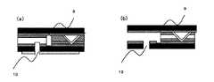
本発明の光ファイバコネクタを、図1〜図6を用いて説明する。
本発明の光ファイバコネクタは、基板1上に光ファイバを固定するための溝8(以下「ファイバ溝」と記載する場合がある。)を有するファイバガイド用コアパターン5が形成された光ファイバガイド部材10と、第1下部クラッド層3上に光信号伝達用コアパターン4が形成され、該光信号伝達用コアパターン上に上部クラッド層6が形成された光導波路20とが並設された構造を有する(図3(f)参照)。The optical fiber connector of the present invention will be described with reference to FIGS.
The optical fiber connector of the present invention is an optical fiber guide in which a
上記光ファイバガイド部材10は、基板1の一部である第2下部クラッド層201上に、ファイバガイド用コアパターン5が形成されることが好ましい。
なお、本発明において、ファイバガイド用コアパターン5は、光ファイバ30を固定するためのものであって、光信号伝達用のコアとして機能するものではない。
また、使用する光ファイバに制限はないが、以下「光ファイバの直径」と表記した場合、光ファイバのクラッド外径もしくは光ファイバの被覆外径を表すこととする。
さらに、上記光ファイバガイド部材10におけるファイバガイド用コアパターン5上には、上部クラッド層を有することが好ましい。該上部クラッド層を有することで、本発明の光ファイバコネクタの平坦性が向上する。In the optical
In the present invention, the fiber
Further, although there is no limitation on the optical fiber to be used, when it is expressed as “optical fiber diameter” below, it represents the cladding outer diameter of the optical fiber or the coating outer diameter of the optical fiber.
Furthermore, it is preferable to have an upper cladding layer on the fiber
本発明において、光ファイバ30は溝8と蓋材7により形成される空間部に差し込まれ、接着剤で固定されるが、このように光ファイバを差し込むだけで光ファイバと光導波路の位置合わせが可能である。
この際、図2に示すX方向の位置合わせはファイバガイド用コアパターン5により行い、図1及び2に示すZ方向の位置合わせは、蓋材7を有する場合には、基板1及び蓋材7の相対的位置を調整することにより行うことができる。また、蓋材7を用いない場合、例えば、ガラスブロック等でファイバを押し込む場合には、基板1とガラスブロック等との相対的位置を調整することにより行うことができる。In the present invention, the
At this time, alignment in the X direction shown in FIG. 2 is performed by the fiber
本発明において、光ファイバの直径は200μm以下であることが、コア層形成用樹脂フィルムの膜厚が制御しやすいという観点から好ましく、125μm径や80μm径の光ファイバを用いることがさらに好ましい。ファイバガイド用コアパターン5の溝8の横幅としては、光ファイバの直径以上の幅であればよいが、光ファイバの実装性及びトレランスの観点から、光ファイバの直径より0.1〜10μm広い幅であることが好ましい。 In the present invention, the diameter of the optical fiber is preferably 200 μm or less from the viewpoint of easy control of the film thickness of the core layer forming resin film, and it is more preferable to use an optical fiber having a diameter of 125 μm or 80 μm. The lateral width of the
本発明の特徴は、光ファイバガイド部材に接着剤導入スリット13を設けた点である。該接着剤導入スリットによって、光ファイバ30を光ファイバガイド部材10に容易に固定することができ、基板によらずに光ファイバと光導波路コアとの位置合わせが容易となり、光ファイバの位置ずれがしにくい上に、確実かつ簡便に光ファイバと光導波路を接続することができる A feature of the present invention is that an adhesive introduction slit 13 is provided in the optical fiber guide member. With the adhesive introduction slit, the
接着剤導入スリット13は、本発明の効果を奏する範囲で種々の場所に設けることができる。いくつかの態様について、以下具体例を示しながら説明する。なお、以下に説明する態様では、光ファイバガイド部材10が、ファイバガイド用コアパターン5を覆う蓋材7を有しているため、光ファイバは、各図の左側から差し込まれる形で挿入され、接着剤導入スリット13から接着剤が導入されて、光ファイバを光ファイバガイド部材に固着させるものである。但し、本発明はこのような蓋材付きのものに限定されるものではなく、蓋材のないもので、ガラスブロックでファイバを抑えて溝8に押し込み、光信号伝達用コアパターン4の中心と光ファイバ30の中心を位置合わせして、接着剤により固定する態様も包含するものである。 The adhesive introduction slit 13 can be provided in various places as long as the effects of the present invention are achieved. Several aspects will be described below with specific examples. In the embodiment described below, since the optical
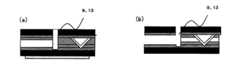
図1(a)−10及び(b)−10は、それぞれ光ファイバを固定するための溝部分の断面図及び光ファイバガイド用コア部分の断面図である。この態様(以下「第1の態様」と称する。)では、接着剤導入スリット13を、光導波路端面を切削するように基板1側から設けるものである。
次に、図4に示す態様(以下「第2の態様」と称する。)では、接着剤導入スリット13を、光導波路端面を切削するように蓋材7側から設けるものである。
また、図5に示す態様(以下「第3の態様」と称する。)では、接着剤導入スリット13を、光導波路端面から離れた位置に、基板1側から設けるものである。
さらに、図6に示す態様(以下「第4の態様」と称する。)では、接着剤導入スリット13を、光導波路端面から離れた位置に、蓋材7側から設けるものである。
なお、スリットを設ける方法としては特に限定されず、例えばダイシングソーによって切削することで形成することができる。FIGS. 1 (a) -10 and (b) -10 are a sectional view of a groove portion for fixing an optical fiber and a sectional view of a core portion for an optical fiber guide, respectively. In this mode (hereinafter referred to as “first mode”), the adhesive introduction slit 13 is provided from the
Next, in the embodiment shown in FIG. 4 (hereinafter referred to as “second embodiment”), the adhesive introduction slit 13 is provided from the
In the mode shown in FIG. 5 (hereinafter referred to as “third mode”), the adhesive introduction slit 13 is provided from the
Further, in the embodiment shown in FIG. 6 (hereinafter referred to as “fourth embodiment”), the adhesive introduction slit 13 is provided from the
In addition, it does not specifically limit as a method to provide a slit, For example, it can form by cutting with a dicing saw.
上記4態様のうち、第1の態様及び第2の態様では、接着剤導入スリット13は、後に詳述するスリット溝9の役割を兼ね備えるものであり、光導波路端面を平滑化しつつ、接着剤導入路を確保できる点で好ましい。また、製造工程としても2つの工程を兼ね備えることができ好ましい。
また、第1の態様及び第4の態様では、接着剤導入スリット13が電気配線板103側にあるために、光ファイバの接着と素子の実装とが同一面側で行えるという利点があり好ましい。
また、第2の態様及び第3の態様では、接着剤導入スリット13が蓋材7側にあるために、溢れた接着剤が、素子の実装端子を侵すことがないため、作業性が良く行えるという利点があり好ましい。Among the above four modes, in the first mode and the second mode, the adhesive introduction slit 13 also has a role of a
In the first and fourth aspects, since the adhesive introduction slit 13 is on the
In the second and third aspects, since the adhesive introduction slit 13 is on the
以下、本発明の光ファイバコネクタを構成する各層について説明する。
(下部クラッド層及び上部クラッド層)
以下、本発明で使用される下部クラッド層(第1下部クラッド層、第2下部クラッド層)201、3及び上部クラッド層6について説明する。下部クラッド層201、3及び上部クラッド層6としては、クラッド層形成用樹脂又はクラッド層形成用樹脂フィルムを用いることができる。Hereinafter, each layer constituting the optical fiber connector of the present invention will be described.
(Lower cladding layer and upper cladding layer)
Hereinafter, the lower clad layers (first lower clad layer, second lower clad layer) 201 and 3 and the upper clad
本発明で用いるクラッド層形成用樹脂としては、光信号伝達用コアパターン4より低屈折率で、光又は熱により硬化する樹脂組成物であれば特に限定されず、熱硬化性樹脂組成物や感光性樹脂組成物を好適に使用することができる。クラッド層形成用樹脂に用いる樹脂組成物は、下部クラッド層201、3及び上部クラッド層6において、該樹脂組成物に含有する成分が同一であっても異なっていてもよく、該樹脂組成物の屈折率が同一であっても異なっていてもよい。また、第2下部クラッド層201については、接着層2としての機能があれば、屈折率や光硬化性の性質は必要なく、後述の接着剤やコア形成用樹脂フィルムを用いてもよい。 The clad layer forming resin used in the present invention is not particularly limited as long as it is a resin composition that has a lower refractive index than the optical signal
本発明においては、クラッド層の形成方法は特に限定されず、例えば、クラッド層形成用樹脂の塗布又はクラッド層形成用樹脂フィルムのラミネートにより形成すればよい。
塗布による場合には、その方法は限定されず、クラッド層形成用樹脂組成物を常法により塗布すればよい。
また、ラミネートに用いるクラッド層形成用樹脂フィルムは、例えば、クラッド層形成用樹脂組成物を溶媒に溶解して、キャリアフィルムに塗布し、溶媒を除去することにより容易に製造することができる。In the present invention, the method for forming the clad layer is not particularly limited, and for example, the clad layer may be formed by applying a clad layer forming resin or laminating a clad layer forming resin film.
In the case of application, the method is not limited, and the clad layer forming resin composition may be applied by a conventional method.
The clad layer-forming resin film used for laminating can be easily produced by, for example, dissolving the clad layer-forming resin composition in a solvent, applying it to a carrier film, and removing the solvent.
下部クラッド層201、3及び上部クラッド層6の厚さに関しては、特に限定するものではないが、乾燥後の厚さで、5〜500μmの範囲が好ましい。5μm以上であると、光の閉じ込めに必要なクラッド厚さが確保でき、500μm以下であると、膜厚を均一に制御することが容易である。以上の観点から、下部クラッド層201、3及び上部クラッド層6の厚さは、さらに10〜100μmの範囲であることがより好ましい。また、第1下部クラッド層3は、光ファイバの中心と光信号伝達用コアパターンとの中心合わせのため、硬化後のフィルム厚みが、[(光ファイバの半径)−(第1下部クラッド層3上に形成された光信号伝達用コアパターン厚み)/2]の厚みのフィルムを用いることがさらに好ましい。
具体例として、光ファイバの直径80μm、光ファイバのコア径50μmの光ファイバを用いたときの好ましい下部クラッド層3の厚みを示す。まず、光導波路のコア径は、光ファイバから光信号伝達用コアパターンへ光信号が伝搬してくる場合、光ファイバのコア径に外接する正方形が光損失なく伝搬できる。この場合、光導波路のコアは50μm×50μm(コア高さ;50μm)となる。上記の式に当てはめると最適な下部クラッド層3の厚みは15μmとなる。また、上記と同一の光ファイバを用いて、光ファイバから光信号伝達用コアパターンへ光信号が伝搬してくる場合、光ファイバのコア径に内接する正方形が光損失なく伝搬できる。この場合、光導波路のコアは40μm×40μm(コア高さ;40μm)となる。上記の式に当てはめると最適な下部クラッド層3の厚みは20μmとなる。
また、光導波路20において、光信号伝達用コアパターン4を埋め込むための上部クラッド層6の厚みは、コアパターン4の厚さ以上にすることが好ましいが、基板1表面から上部クラッド層上面までの高さが光ファイバの直径以下になるように適宜調整すればよい。The thicknesses of the
As a specific example, a preferable thickness of the
In the
(コア層形成用樹脂及びコア層形成用樹脂フィルム)
本発明においては、下部クラッド層201、3に積層するコア層、光信号伝達用コアパターン4、及びファイバガイド用コアパターン5の形成方法は特に限定されず、例えば、コア層形成用樹脂の塗布又はコア層形成用樹脂フィルムのラミネートによりコア層を形成し、エッチングによりコアパターンを形成すればよい。
本発明においては、光導波路20と光ファイバガイド部材10において、それぞれコア層を形成した後、同時にエッチングして光信号伝達用コアパターン4とファイバガイド用コアパターン5を同時に形成することにより、効率よく光ファイバコネクタを製造することができる。(Core layer forming resin and core layer forming resin film)
In the present invention, the method for forming the core layer laminated on the lower
In the present invention, the
コア層形成用樹脂、特に光信号伝達用コアパターン4に用いるコア層形成用樹脂は、クラッド層3より高屈折率であるように設計され、活性光線によりコアバターンを形成し得る樹脂組成物を用いることが好ましい。パターン化する前のコア層の形成方法は限定されず、前記コア層形成用樹脂組成物を常法により塗布する方法等が挙げられる。 The core layer forming resin, in particular, the core layer forming resin used for the optical signal
コア層形成用樹脂フィルムの厚さについては特に限定されず、乾燥後のコア層の厚さが、通常は10〜100μmとなるように調整される。該フィルムの仕上がり後の光信号伝達用コアパターン4の厚さが10μm以上であると、光導波路形成後の受発光素子又は光ファイバとの結合において位置合わせトレランスが拡大できるという利点があり、100μm以下であると、光導波路形成後の受発光素子又は光ファイバとの結合において、結合効率が向上するという利点がある。以上の観点から、該フィルムの厚さは、さらに30〜90μmの範囲であることが好ましく、該厚みを得るために適宜フィルム厚みを調整すればよい。
また、光信号伝達用コアパターンの硬化後の厚みは、光ファイバから光信号伝達用コアパターンへ光を伝達する場合は、光ファイバのコア径以上になれば光の損失が少なく、光信号伝達用コアパターンから光ファイバへ光を伝達する場合は、光信号伝達用コアパターンの厚さと幅からなる矩形が、光ファイバのコア径の内側になるように調整するとさらによい。The thickness of the resin film for forming the core layer is not particularly limited, and the thickness of the core layer after drying is usually adjusted to be 10 to 100 μm. When the thickness of the optical signal
In addition, when the thickness of the optical signal transmission core pattern after curing is greater than the core diameter of the optical fiber when transmitting light from the optical fiber to the optical signal transmission core pattern, there is less light loss, and optical signal transmission In the case of transmitting light from the optical core pattern to the optical fiber, it is more preferable to adjust the rectangle formed by the thickness and width of the optical signal transmitting core pattern to be inside the core diameter of the optical fiber.
(基板)
基板1の材質としては、特に制限はなく、例えば、ガラスエポキシ樹脂基板、セラミック基板、ガラス基板、シリコン基板、プラスチック基板、金属基板、樹脂層付き基板、金属層付き基板、プラスチックフィルム、樹脂層付きプラスチックフィルム、金属層付きプラスチックフィルム、電気配線板などが挙げられる。
基板1として柔軟性及び強靭性のある基材、例えば、前記クラッド層形成用樹脂フィルム及びコア層形成用樹脂フィルムのキャリアフィルムを基板として用いることで、フレキシブルな光ファイバコネクタとしてもよい。
また、電気配線板は特に限定されるものではないが、金属配線103がFR−4上に形成された電気配線板でもよく、金属配線103がポリイミドやポリアミドフィルム上に形成されたフレキシブル配線板であってもよい。なお、金属配線103は金属層102から形成することができる。(substrate)
There is no restriction | limiting in particular as a material of the board |
The
The electric wiring board is not particularly limited, but may be an electric wiring board in which the
(蓋材)
本発明の光ファイバコネクタは、その好ましい態様として、上記図1〜6に示すように、蓋材7を有する。このような、蓋材7を有する態様では、溝8の深さ及び幅のいずれもが、光ファイバガイド部材の溝に固定される光ファイバ30の直径以上であることが肝要である。すなわち、溝の深さが光ファイバの直径よりも大きく、かつ溝の幅が光ファイバの直径よりも大きいことを要する。この条件を満足することにより、光ファイバを溝と蓋材により形成される空間に容易に差し込むことができる。そして、このように光ファイバを差し込んだ状態で、該光ファイバが、光導波路の光信号伝達用コアパターン4に光信号を伝達可能な位置に接合するように、光ファイバガイド部材10と光導波路20が並設されている。(Cover material)
The optical fiber connector of this invention has the
上記光ファイバガイド部材10における蓋材7の材質としては、特に限定されないが、上部クラッド層6に接着性がある場合、ガラスエポキシ樹脂基板、セラミック基板、ガラス基板、シリコン基板、プラスチック基板、金属基板、プラスチックフィルムが挙げられ、これらの基板には、樹脂層、金属層などが設けられていてもよい。また、蓋材7として、電気配線板を用いることもできる。
特に、柔軟性及び強靭性のある蓋材7として、例えば、ポリエチレンテレフタレート、ポリブチレンテレフタレート、ポリエチレンナフタレート等のポリエステル、ポリエチレン、ポリプロピレン、ポリアミド、ポリカーボネート、ポリフェニレンエーテル、ポリエーテルサルファイド、ポリアリレート、液晶ポリマー、ポリスルホン、ポリエーテルスルホン、ポリエーテルエーテルケトン、ポリエーテルイミド、ポリアミドイミド、ポリイミドなどが好適に挙げられる。これらのうち、耐熱性、寸法安定性の観点から、ポリアミドイミド、ポリイミドが特に好ましい。The material of the
In particular, as the
また、上部クラッド層6に接着性が無い場合、上記に列挙した蓋材7に接着層を設け、接着層付きの蓋材7とすることが好ましい。
蓋材7の厚さとしては、板の反りや寸法安定性により、適宜変更し得るが、好ましくは10μm〜10.0mmである。また、蓋材7に形成する接着層の厚さとしては、通常、0.1μm〜50μmが好適な範囲であるが、0.1μm〜20μmがより好ましい。接着層の厚さが20μm以下であると、溝8への接着剤の流れ込みが抑制されるためである。
さらに、本発明における光導波路は光路変換ミラー11を有することが好ましく、その場合には、該蓋材7が光路変換ミラー11の補強板を兼ね備えていることが好ましい。Further, when the upper clad
The thickness of the
Furthermore, the optical waveguide in the present invention preferably has an optical
(接着剤)
上記接着剤導入スリットに用いられる接着剤としては、光ファイバと光ファイバガイド部材を接着し得るものであれば特に制限はないが、光学用接着剤、光路結合用接着剤、光学部品用シール材、透明接着剤、屈折率整合材兼接着剤、クラッド層形成用樹脂ワニス、コア層形成用樹脂ワニスなどの光硬化型接着剤、熱硬化型接着剤、光熱硬化型の接着剤、2液混合硬化型の接着剤が挙げられ、これらのうち、基板1や蓋材7が、硬化させるための電磁波を透過しない場合には、熱硬化型の接着剤又は、2液混合硬化型の接着剤が好ましい。(adhesive)
The adhesive used for the adhesive introduction slit is not particularly limited as long as it can bond an optical fiber and an optical fiber guide member. However, an optical adhesive, an optical path coupling adhesive, and an optical component sealing material. , Transparent adhesive, refractive index matching material / adhesive, clad layer forming resin varnish, core layer forming resin varnish, etc., photocurable adhesive, thermosetting adhesive, photothermosetting adhesive, two-component mixture A curable adhesive can be used, and among these, when the
(本発明の光ファイバコネクタの製造方法)
本発明の製造方法は、以下の3つの工程を順に有することを特徴とする。すなわち、
(1)基板上に第1下部クラッド層形成用フィルムを積層し、該第1下部クラッド層形成用フィルムをエッチングによって、光ファイバを固定するための溝を形成する部位の第1下部クラッド層形成用フィルムを除去する工程、
(2)該第1下部クラッド層及び上記(1)の工程によって第1下部クラッド層形成用フィルムが除去された基板上に、コア形成用フィルムを積層し、エッチングによって、ファイバガイド用コアパターンと光信号伝達用コアパターンを一括形成する工程、及び
(3)光ファイバガイド部材の基板側から接着剤導入スリットを設ける工程を順に有する光ファイバコネクタの製造方法である。(Manufacturing method of optical fiber connector of the present invention)
The manufacturing method of the present invention is characterized by having the following three steps in order. That is,
(1) First lower clad layer forming film is laminated on a substrate, and the first lower clad layer forming film is etched to form a first lower clad layer at a portion where a groove for fixing an optical fiber is formed. Removing the film,
(2) A core forming film is laminated on the first lower clad layer and the substrate from which the first lower clad layer forming film has been removed in the step (1), and the fiber guide core pattern is formed by etching. An optical fiber connector manufacturing method comprising sequentially forming a core pattern for transmitting an optical signal and (3) providing an adhesive introduction slit from the substrate side of the optical fiber guide member.
上記(1)の工程は、光ファイバコネクタ中の、光導波路の部分のみ第1下部クラッド層を形成し、光ファイバガイド部材の部位からは第1下部クラッド層を除去するものである。このことにより、光導波路においては、光伝送のための下部クラッドを形成するとともに、光導波路と光ファイバのZ方向の位置合わせを行うものである。したがって、第1下部クラッド層の厚さは、用いる光ファイバの径に応じて適宜設定されるものであり、好適な厚さは上述の通りである。
次に(2)の工程によって、光導波路においては、第1下部クラッド層上に光信号伝達用コアパターンを形成し、光ファイバガイド部材においては、基板上に光ファイバを固定するためのファイバガイド用コアパターンを形成する。
最後に、(3)の工程によって、光ファイバガイド部材の基板側から接着剤導入スリットを設けるものである。スリットを設ける方法としては特に制限はないが、ダイシングソーによって切削する方法が簡便で好ましい。In the step (1), the first lower cladding layer is formed only in the portion of the optical waveguide in the optical fiber connector, and the first lower cladding layer is removed from the portion of the optical fiber guide member. Thus, in the optical waveguide, a lower clad for optical transmission is formed, and the optical waveguide and the optical fiber are aligned in the Z direction. Therefore, the thickness of the first lower cladding layer is appropriately set according to the diameter of the optical fiber to be used, and the preferred thickness is as described above.
Next, by the step (2), in the optical waveguide, an optical signal transmission core pattern is formed on the first lower cladding layer, and in the optical fiber guide member, a fiber guide for fixing the optical fiber on the substrate. A core pattern is formed.
Finally, an adhesive introduction slit is provided from the substrate side of the optical fiber guide member by the step (3). Although there is no restriction | limiting in particular as a method of providing a slit, The method of cutting with a dicing saw is simple and preferable.
また、次のような工程からなる製造方法も本発明の方法である。すなわち、上記(1)の工程及び(2)の工程に次いで、
(4)少なくとも該ファイバガイド用コアパターンを覆う蓋材を形成する工程、及び(5)該蓋材側から接着剤導入スリットを設ける工程を有する光ファイバコネクタの製造方法である。
上記(4)の工程において、蓋材の形成方法は蓋材の材質に応じて適宜決定されるが、ロールラミネータ、真空ラミネータなどを用いて形成することが好ましい。
また、(5)の工程は、上記(3)の工程と同様である。Moreover, the manufacturing method which consists of the following processes is also the method of this invention. That is, following the steps (1) and (2) above,
(4) A method for manufacturing an optical fiber connector, comprising: a step of forming a cover material covering at least the fiber guide core pattern; and (5) a step of providing an adhesive introduction slit from the cover material side.
In the step (4), the method of forming the lid is appropriately determined according to the material of the lid, but it is preferably formed using a roll laminator, a vacuum laminator or the like.
The step (5) is the same as the step (3).
また、上述の本発明の製造方法では、前記(2)の工程、すなわち、ファイバガイド用コアパターンと光信号伝達用コアパターンを一括形成する工程の後に、ファイバガイド用コアパターンと光信号伝達用コアパターン形成面側から、上部クラッド層形成用フィルムを積層し、エッチングによって、光ファイバを固定するための溝部分の上部クラッド層形成用フィルムを除去する工程を有することが好ましい。
この工程によって、光導波路においては、上部クラッド層が形成され、高い光伝達効率が達成される。一方、光ファイバガイド部材においては、溝を確保するために、その部分のクラッド層がエッチングによって除去されるものである。ここで、ファイバガイド用コアパターン上の上部クラッド層は、エッチングによって除去してもよいし、残してもよいが、平坦性を確保するために、ファイバガイド用コアパターン上の上部クラッド層は残すことが好ましい。なお、溝8部分の上部クラッド層形成用樹脂フィルムをエッチング除去する工程において、除去部分が、ファイバガイド用コアパターン上にかかっていてもよい。In the manufacturing method of the present invention described above, after the step (2), ie, the step of forming the fiber guide core pattern and the optical signal transmission core pattern at once, the fiber guide core pattern and the optical signal transmission It is preferable to have a step of laminating an upper clad layer forming film from the core pattern forming surface side and removing the upper clad layer forming film in the groove portion for fixing the optical fiber by etching.
By this step, an upper cladding layer is formed in the optical waveguide, and high light transmission efficiency is achieved. On the other hand, in the optical fiber guide member, in order to secure a groove, the cladding layer in that portion is removed by etching. Here, the upper clad layer on the fiber guide core pattern may be removed by etching or may be left, but the upper clad layer on the fiber guide core pattern is left in order to ensure flatness. It is preferable. In the step of etching and removing the upper clad layer forming resin film in the
なお、本発明の製造方法では、接着剤導入スリット13がスリット溝9を兼用する場合には、スリット溝9を別途設ける必要はないが、スリット溝9と異なる位置に接着剤層導入スリット13を設ける場合には、スリット溝9を設けることが好ましい。この場合のスリット溝9の形成方法としては特に制限はなく、ダイシングソーによってスリット溝を形成することが好適に行われる。なお、スリット溝9の深さは、第1下部クラッド層表面以下であることが好ましい。
スリット溝9を設ける工程によって、後述するように、光ファイバと光導波路を接続する光導波路端面が平滑化される。また、スリットの深さを上記のようにすることによって、光ファイバが良好に実装できる。In the manufacturing method of the present invention, when the adhesive introduction slit 13 also serves as the
By providing the
また、光信号伝達用コアパターン4、ファイバガイド用コアパターン5が、特に基板1に密着性が無い場合には、接着層2付きの基板1を用いてもよく、接着層が第2下部クラッド層201を兼用していてもよい。
接着層2の種類としては特に限定されないが、両面テープ、UVまたは熱硬化性接着剤、プリプレグ、ビルドアップ材、電気配線板製造用途に使用される種々の接着剤が好適に挙げられる。光信号が基板1を透過する場合には、光信号波長において透明であればよくその際には、基板1と接着力のあるクラッド層形成用樹脂フィルムやコア層形成用樹脂フィルムを用いて接着層2とするのが好ましい。Further, when the optical signal
Although it does not specifically limit as a kind of
光ファイバと光導波路を接続する光導波路端面の平滑化方法としては、特に限定するものではないが、例えば、ダイシングソーを用いて光導波路端面を切削し、スリット溝9を形成すると共に平滑化すればよい。この際のダイシングブレードの切削深さは、基板1表面以下にすると光ファイバ30が良好に実装できるため好ましい。 The method for smoothing the end face of the optical waveguide that connects the optical fiber and the optical waveguide is not particularly limited. That's fine. The cutting depth of the dicing blade at this time is preferably less than the surface of the
以下、本発明を実施例によりさらに詳細に説明するが、本発明はその要旨を越えない限り、以下の実施例に限定されない。
実施例1
[クラッド層形成用樹脂フィルムの作製]
[(A)ベースポリマー;(メタ)アクリルポリマー(A−1)の作製]
撹拌機、冷却管、ガス導入管、滴下ろうと、及び温度計を備えたフラスコに、プロピレングリコールモノメチルエーテルアセテート46質量部及び乳酸メチル23質量部を秤量し、窒素ガスを導入しながら撹拌を行った。液温を65℃に上昇させ、メチルメタクリレート47質量部、ブチルアクリレート33質量部、2−ヒドロキシエチルメタクリレート16質量部、メタクリル酸14質量部、2,2’−アゾビス(2,4−ジメチルバレロニトリル)3質量部、プロピレングリコールモノメチルエーテルアセテート46質量部、及び乳酸メチル23質量部の混合物を3時間かけて滴下後、65℃で3時間撹拌し、さらに95℃で1時間撹拌を続けて、(メタ)アクリルポリマー(A−1)溶液(固形分45質量%)を得た。
[重量平均分子量の測定]
(A−1)の重量平均分子量(標準ポリスチレン換算)をGPC(東ソー(株)製「SD−8022」、「DP−8020」、及び「RI−8020」)を用いて測定した結果、3.9×10⁴であった。なお、カラムは日立化成工業(株)製「Gelpack GL−A150−S」及び「Gelpack GL−A160−S」を使用した。
[酸価の測定]
(A−1)の酸価を測定した結果、79mgKOH/gであった。なお、酸価は(A−1)溶液を中和するのに要した0.1mol/L水酸化カリウム水溶液量から算出した。このとき、指示薬として添加したフェノールフタレインが無色からピンク色に変色した点を中和点とした。
[クラッド層形成用樹脂ワニスAの調合]
(A)ベースポリマーとして、前記A−1溶液(固形分45質量%)84質量部(固形分38質量部)、(B)光硬化成分として、ポリエステル骨格を有するウレタン(メタ)アクリレート(新中村化学工業(株)製「U−200AX」)33質量部、及びポリプロピレングリコール骨格を有するウレタン(メタ)アクリレート(新中村化学工業(株)製「UA−4200」)15質量部、(C)熱硬化成分として、ヘキサメチレンジイソシアネートのイソシアヌレート型三量体をメチルエチルケトンオキシムで保護した多官能ブロックイソシアネート溶液(固形分75質量%)(住化バイエルウレタン(株)製「スミジュールBL3175」)20質量部(固形分15質量部)、(D)光重合開始剤として、1−[4−(2−ヒドロキシエトキシ)フェニル]−2−ヒドロキシ−2−メチル−1−プロパン−1−オン(チバ・ジャパン(株)製「イルガキュア2959」)1質量部、ビス(2,4,6−トリメチルベンゾイル)フェニルホスフィンオキシド(チバ・ジャパン(株)製「イルガキュア819」)1質量部、及び希釈用有機溶剤としてプロピレングリコールモノメチルエーテルアセテート23質量部を攪拌しながら混合した。孔径2μmのポリフロンフィルタ(アドバンテック東洋(株)製「PF020」)を用いて加圧濾過後、減圧脱泡し、クラッド層形成用樹脂ワニスを得た。
上記で得られたクラッド層形成用樹脂ワニスAを、PETフィルム(東洋紡績(株)製「コスモシャインA4100」、厚み50μm)の非処理面上に、塗工機(マルチコーターTM−MC、株式会社ヒラノテクシード製)を用いて塗布し、100℃で20分乾燥後、保護フィルムとして表面離型処理PETフィルム(帝人デュポンフィルム(株)製「ピューレックスA31」、厚み25μm)を貼付け、クラッド層形成用樹脂フィルムを得た。このとき樹脂層の厚みは、塗工機のギャップを調節することで任意に調整可能であり、本実施例では使用した第1下部クラッド層及び第2下部クラッド層(接着層)の厚みに付いては、実施例中に記載する。また、第1下部クラッド層及び第2下部クラッド層の硬化後の膜厚と塗工後の膜厚は同一であった。本実施例で用いた上部クラッド層形成用樹脂フィルムの膜厚についても実施例中に記載する。実施例中に記載する上部クラッド層形成用樹脂フィルムの膜厚は塗工後の膜厚とする。EXAMPLES Hereinafter, although an Example demonstrates this invention further in detail, this invention is not limited to a following example, unless the summary is exceeded.
Example 1
[Preparation of resin film for forming clad layer]
[(A) Base polymer; production of (meth) acrylic polymer (A-1)]
46 parts by mass of propylene glycol monomethyl ether acetate and 23 parts by mass of methyl lactate were weighed in a flask equipped with a stirrer, a cooling pipe, a gas introduction pipe, a dropping funnel, and a thermometer, and stirred while introducing nitrogen gas. . The liquid temperature was raised to 65 ° C., 47 parts by weight of methyl methacrylate, 33 parts by weight of butyl acrylate, 16 parts by weight of 2-hydroxyethyl methacrylate, 14 parts by weight of methacrylic acid, 2,2′-azobis (2,4-dimethylvaleronitrile ) A mixture of 3 parts by mass, 46 parts by mass of propylene glycol monomethyl ether acetate and 23 parts by mass of methyl lactate was added dropwise over 3 hours, followed by stirring at 65 ° C. for 3 hours, and further stirring at 95 ° C. for 1 hour. A (meth) acrylic polymer (A-1) solution (solid content: 45% by mass) was obtained.
[Measurement of weight average molecular weight]
As a result of measuring the weight average molecular weight (in terms of standard polystyrene) of (A-1) using GPC (“SD-8022”, “DP-8020”, and “RI-8020” manufactured by Tosoh Corporation), 3. It was 9 × 10⁴ . The column used was “Gelpack GL-A150-S” and “Gelpack GL-A160-S” manufactured by Hitachi Chemical Co., Ltd.
[Measurement of acid value]
As a result of measuring the acid value of (A-1), it was 79 mgKOH / g. In addition, the acid value was computed from the amount of 0.1 mol / L potassium hydroxide aqueous solution required for neutralizing the (A-1) solution. At this time, the point at which the phenolphthalein added as an indicator changed color from colorless to pink was defined as the neutralization point.
[Preparation of Cladding Layer Forming Resin Varnish A]
(A) As the base polymer, 84 parts by mass (solid content: 45% by mass) of the A-1 solution (solid content: 45% by mass), (B) Urethane (meth) acrylate having a polyester skeleton as the photocuring component (Shin Nakamura) 33 parts by mass of “U-200AX” manufactured by Chemical Industry Co., Ltd., and 15 parts by mass of urethane (meth) acrylate having a polypropylene glycol skeleton (“UA-4200” manufactured by Shin-Nakamura Chemical Co., Ltd.), (C) heat As a curing component, 20 parts by mass of a polyfunctional block isocyanate solution (solid content: 75% by mass) obtained by protecting an isocyanurate type trimer of hexamethylene diisocyanate with methyl ethyl ketone oxime (“Sumijour BL3175” manufactured by Sumika Bayer Urethane Co., Ltd.) (Solid content 15 parts by mass), (D) As a photopolymerization initiator, 1- [4- (2-hydroxy ester) Xyl) phenyl] -2-hydroxy-2-methyl-1-propan-1-one (“Irgacure 2959” manufactured by Ciba Japan Co., Ltd.), 1 part by mass, bis (2,4,6-trimethylbenzoyl) phenylphosphine 1 part by mass of oxide (“Irgacure 819” manufactured by Ciba Japan Co., Ltd.) and 23 parts by mass of propylene glycol monomethyl ether acetate as an organic solvent for dilution were mixed with stirring. After pressure filtration using a polyflon filter having a pore size of 2 μm (“PF020” manufactured by Advantech Toyo Co., Ltd.), degassing was performed under reduced pressure to obtain a resin varnish for forming a cladding layer.
The resin varnish A for forming a clad layer obtained above is coated on a non-treated surface of a PET film (“Cosmo Shine A4100” manufactured by Toyobo Co., Ltd., thickness 50 μm) (multicoater TM-MC, stock) After applying for 20 minutes at 100 ° C., surface release treated PET film (“Purex A31” manufactured by Teijin DuPont Films Co., Ltd., thickness 25 μm) is applied as a protective film to form a cladding layer A resin film was obtained. At this time, the thickness of the resin layer can be arbitrarily adjusted by adjusting the gap of the coating machine. In this embodiment, the thickness of the first lower cladding layer and the second lower cladding layer (adhesive layer) is used. Are described in the Examples. Moreover, the film thickness after hardening of the 1st lower clad layer and the 2nd lower clad layer and the film thickness after coating were the same. The film thickness of the upper clad layer forming resin film used in this example is also described in the examples. The film thickness of the upper clad layer forming resin film described in the examples is the film thickness after coating.
[コア層形成用樹脂フィルムの作製]
(A)ベースポリマーとして、フェノキシ樹脂(商品名:フェノトートYP−70、東都化成(株)製)26質量部、(B)光重合性化合物として、9,9−ビス[4−(2−アクリロイルオキシエトキシ)フェニル]フルオレン(商品名:A−BPEF、新中村化学工業(株)製)36質量部、及びビスフェノールA型エポキシアクリレート(商品名:EA−1020、新中村化学工業(株)製)36質量部、(C)光重合開始剤として、ビス(2,4,6−トリメチルベンゾイル)フェニルフォスフィンオキサイド(商品名:イルガキュア819、チバ・ジャパン(株)製)1質量部、及び1−[4−(2−ヒドロキシエトキシ)フェニル]−2−ヒドロキシ−2−メチル−1−プロパン−1−オン(商品名:イルガキュア2959、チバ・ジャパン(株)社製)1質量部、有機溶剤としてプロピレングリコールモノメチルエーテルアセテート40質量部を用いたこと以外は上記クラッド層形成用樹脂ワニスAの製造例と同様の方法及び条件でコア層形成用樹脂ワニスBを調合した。その後、上記クラッド層形成用樹脂ワニスAの製造例と同様の方法及び条件で加圧濾過し、さらに減圧脱泡した。
上記で得られたコア層形成用樹脂ワニスBを、PETフィルム(商品名:コスモシャインA1517、東洋紡績(株)製、厚さ:16μm)の非処理面上に、上記製造例と同様な方法で塗布乾燥し、次いで保護フィルムとして離型PETフィルム(商品名:ピューレックスA31、帝人デュポンフィルム(株)製、厚さ:25μm)を離型面が樹脂側になるように貼り付け、コア層形成用樹脂フィルムを得た。このとき樹脂層の厚みは、塗工機のギャップを調節することで任意に調整可能であり、本実施例では使用したコア層形成用樹脂フィルム厚みに付いては、以下の各実施例中に記載する。実施例中に記載するコア層形成用樹脂フィルムの膜厚は塗工後の膜厚とする。[Preparation of resin film for core layer formation]
(A) As a base polymer, 26 parts by mass of a phenoxy resin (trade name: Phenotote YP-70, manufactured by Toto Kasei Co., Ltd.), and (B) 9,9-bis [4- (2- Acrylyloxyethoxy) phenyl] fluorene (trade name: A-BPEF, Shin-Nakamura Chemical Co., Ltd.) 36 parts by mass, and bisphenol A type epoxy acrylate (trade name: EA-1020, Shin-Nakamura Chemical Co., Ltd.) ) 36 parts by mass, (C) As a photopolymerization initiator, 1 part by mass of bis (2,4,6-trimethylbenzoyl) phenylphosphine oxide (trade name: Irgacure 819, manufactured by Ciba Japan Co., Ltd.), and 1 -[4- (2-hydroxyethoxy) phenyl] -2-hydroxy-2-methyl-1-propan-1-one (trade name: Irgacure 2959, Chi -Made by Japan Co., Ltd.) Core layer formation under the same method and conditions as in the above production example of resin varnish A for forming a cladding layer except that 1 part by mass and 40 parts by mass of propylene glycol monomethyl ether acetate as an organic solvent were used. Resin varnish B was prepared. Then, pressure filtration was carried out under the same method and conditions as in the production example of the resin varnish A for forming a cladding layer, and degassing was further performed.
The resin layer varnish B for core layer formation obtained above is applied to a non-treated surface of a PET film (trade name: Cosmo Shine A1517, manufactured by Toyobo Co., Ltd., thickness: 16 μm) in the same manner as in the above production example. Then, a release PET film (trade name: Purex A31, manufactured by Teijin DuPont Films, Inc., thickness: 25 μm) is applied as a protective film so that the release surface is on the resin side, and the core layer A forming resin film was obtained. At this time, the thickness of the resin layer can be arbitrarily adjusted by adjusting the gap of the coating machine. In this example, the thickness of the resin film for forming the core layer used in this example is described in the following examples. Describe. The film thickness of the core layer forming resin film described in the examples is the film thickness after coating.
[基板の作製]
(サブトラクティブ法による電気配線形成)
金属層102として片面銅箔付きのポリイミドフィルム101((ポリイミド;ユーピレックスVT(宇部日東化成(株)製)、厚み;25μm)、(銅箔;NA−DFF(三井金属鉱業(株)製))、厚み;9μm)(図1(a)−1、図2(c)−1参照)の銅箔面に感光性ドライフィルムレジスト(商品名:フォテック、日立化成工業(株)製、厚さ:25μm)をロールラミネータ(日立化成テクノプラント(株)製、HLM−1500)を用い圧力0.4MPa、温度110℃、ラミネート速度0.4m/minの条件で貼り、次いで紫外線露光機((株)オーク製作所製、EXM−1172)にて感光性ドライフィルムレジスト側から幅50μmのネガ型フォトマスクを介し、紫外線(波長365nm)を120mJ/cm2照射し、未露光部分の感光性ドライフィルムレジストを35℃の0.1〜5重量%炭酸ナトリウムの希薄溶液で除去した。その後、塩化第二鉄溶液を用いて、感光性ドライフィルムレジストが除去されむき出しになった部分の銅箔をエッチングにより除去し、35℃の1〜10重量%水酸化ナトリウム水溶液を用いて、露光部分の感光性ドライフィルムレジストを除去し、L(ライン幅)/S(間隙幅)=60/65μmの電気配線103を形成しフレキシブル配線板を得た。[Production of substrate]
(Electric wiring formation by subtractive method)
(Ni/Auめっきの形成)
その後、フレキシブル配線板を、脱脂、ソフトエッチング、酸洗浄し、無電解Niめっき用増感剤(商品名:SA−100、日立化成工業(株)製)に25℃で5分間浸漬後水洗し、83℃の無電解Niめっき液(奥野製薬(株)製、ICPニコロンGM−SD溶液、pH4.6)に8分間浸漬して3μmのNi被膜を形成し、その後、純水にて洗浄を実施した。
次に、置換金めっき液(100mL;HGS−500及び1.5g;シアン化金カリウム/Lで建浴)(商品名:HGS−500、日立化成工業(株)製、)に85℃で8分間浸漬し、Ni被膜上に0.06μmの置換金被膜を形成した。これにより、カバーレイフィルムのない電気配線103部分が、Ni及びAuのめっきに被覆されたフレキシブル配線板を得た(図1(a)−2、図2(c)−2参照)。
接着層2として上記で得られた10μm厚のクラッド層形成用樹脂フィルムを大きさ100×100mmに裁断し、保護フィルムである離型PETフィルム(ピューレックスA31)を剥離し、上記で形成したフレキシブル配線板のポリイミド面に、平板型ラミネータとして真空加圧式ラミネータ((株)名機製作所製、MVLP−500)を用い、500Pa以下に真空引きした後、圧力0.4MPa、温度100℃、加圧時間30秒の条件にて加熱圧着して、第2下部クラッド層201付きの電気配線板を形成した。紫外線露光機((株)オーク製作所製、EXM−1172)にてキャリアフィルム側から紫外線(波長365nm)を4J/cm2照射し、次いでキャリアフィルムを剥離し、170℃で1時間加熱処理することにより、厚さ10μmの第2下部クラッド層201付きの基板1を形成した(図1(a)−3、図2(c)−3参照)。(Formation of Ni / Au plating)
Thereafter, the flexible wiring board is degreased, soft etched, acid washed, immersed in an electroless Ni plating sensitizer (trade name: SA-100, manufactured by Hitachi Chemical Co., Ltd.) at 25 ° C. for 5 minutes and then washed with water. , Immersed in an electroless Ni plating solution (Okuno Pharmaceutical Co., Ltd., ICP Nicolon GM-SD solution, pH 4.6) at 83 ° C. for 8 minutes to form a 3 μm Ni film, and then washed with pure water Carried out.
Next, the displacement gold plating solution (100 mL; HGS-500 and 1.5 g; built-in bath with potassium gold cyanide / L) (trade name: HGS-500, manufactured by Hitachi Chemical Co., Ltd.), 8 at 85 ° C. It was immersed for a minute to form a 0.06 μm displacement gold film on the Ni film. Thereby, the flexible wiring board by which the
The 10 μm-thick clad layer-forming resin film obtained above as the
[光ファイバコネクタの作製]
上記で得られた15μm厚の下部クラッド層形成用樹脂フィルムを大きさ100×100μmに裁断し、保護フィルムを剥離して、第2下部クラッド層201面側に上記と同様の条件で、真空ラミネータによって積層した。95μm×3.0mm×4本の非露光部を有したネガ型フォトマスクを介し、紫外線露光機((株)オーク製作所製、EXM−1172)にてキャリアフィルム側から紫外線(波長365nm)を250mJ/cm2照射した。その後、キャリアフィルムを剥離し、現像液(1%炭酸カリウム水溶液)を用いて、第1下部クラッド層3をエッチングした。続いて、水洗浄し、170℃で1時間加熱乾燥及び硬化し、光ファイバ溝形成部分に95μm×3.0mmの開口部を形成した第1下部クラッド層3付きの基板1を作製した(図1(a)−4、図2(c)−4、図2(d)−4参照)。これにより、光導波路20形成部分には、第1下部クラッド層3が形成され、光ファイバを搭載する溝8部分には、第1下部クラッド層3が無い状態となっている。
次に、上記の第1下部クラッド層3面にロールラミネータ(日立化成テクノプラント(株)製、HLM−1500)を用い圧力0.4MPa、温度50℃、ラミネート速度0.2m/minの条件で、保護フィルムを剥離した50μm厚の上記コア層形成用樹脂フィルムをラミネートし、次いで上記の真空加圧式ラミネータ(株式会社名機製作所製、MVLP−500)を用い、500Pa以下に真空引きした後、圧力0.4MPa、温度70℃、加圧時間30秒の条件にて加熱圧着した。その後、光信号伝達用コアパターン幅50μm(光ファイバ接続部分のパターンピッチ;125μm、光路変換ミラー形成部(光ファイバ接続部分より5mm地点)のパターンピッチ;250μm、4本)、ファイバガイド用コアパターン幅40μm(ファイバ溝ピッチ;125μm、4本、両端のファイバガイド用コアパターンのみ150μm)のネガ型フォトマスクを介し、光信号伝達用コアパターン4が第1下部クラッド層3上に、ファイバガイド用コアパターン5によって形成される溝8が基板1(第2下部クラッド層201)上に形成されるように位置合わせをし、上記紫外線露光機にて紫外線(波長365nm)を700mJ/cm2照射し、次いで80℃で5分間露光後加熱を行った。その後、キャリアフィルムであるPETフィルムを剥離し、現像液(プロピレングリコールモノメチルエーテルアセテート/N,N−ジメチルアセトアミド=8/2、質量比)を用いて、コアパターンをエッチングした。続いて、洗浄液(イソプロパノール)を用いて洗浄し、100℃で10分間加熱乾燥し、光信号伝達用コアパターン4及びファイバガイド用コアパターン5を形成し、同時に85μm幅の溝8が形成された。なお、ファイバガイド用コアパターン5における各パターンの大きさは、光ファイバを溝8に固定した際に、光ファイバが光信号伝達用コアパターン4に光信号を送受可能な位置に接合するように設計されている(図1(a)−5、図1(b)−5、図2(c)−5、図2(d)−5、図2(e)参照)。[Fabrication of optical fiber connector]
The 15 μm-thick lower clad layer-forming resin film obtained above is cut into a size of 100 × 100 μm, the protective film is peeled off, and a vacuum laminator is formed on the second lower clad layer 201 surface side under the same conditions as described above. Laminated. Through a negative photomask having 95 μm × 3.0 mm × 4 non-exposed portions, UV light (wavelength 365 nm) is 250 mJ from the carrier film side with an ultraviolet light exposure machine (EXM-1172, manufactured by Oak Manufacturing Co., Ltd.). / Cm2 irradiation. Thereafter, the carrier film was peeled off, and the first
Next, a roll laminator (manufactured by Hitachi Chemical Technoplant Co., Ltd., HLM-1500) is used on the surface of the first
次いで、保護フィルムを剥離した85μm厚の上部クラッド層樹脂フィルムをコアパターン形成面側から上記の真空加圧式ラミネータ((株)名機製作所製、MVLP−500)を用い、500Pa以下に真空引きした後、圧力0.4MPa、温度110℃、加圧時間30秒の条件にて加熱圧着して、ラミネートした。さらに、第1下部クラッド層3形成の際に使用したネガ型フォトマスクを使用して紫外線(波長365nm)を150mJ/cm2照射後、キャリアフィルムを剥離し、現像液(1%炭酸カリウム水溶液)を用いて、溝8部分の上部クラッド層形成用樹脂フィルムをエッチングした。続いて、水洗浄し、170℃で1時間加熱乾燥及び硬化した。
以上のようにして、125μmピッチ、ファイバ径80μm、4チャンネル用の光ファイバコネクタを作製した。
得られた光ファイバコネクタにおいて、ファイバガイド用コアパターン5の溝8の横幅は85μm、ファイバガイド用コアパターン5の高さ(第2下部クラッド層201表面からの高さ)は64μm、基板面から上部クラッド層上面までの高さは85.5μm、光信号伝達用コアパターン4の厚みは50μmであった(図1(a)−6、図1(b)−6、図2(c)−6、図2(d)−6、図3(f)参照)。Next, the 85 μm thick upper clad layer resin film from which the protective film was peeled was evacuated to 500 Pa or less from the core pattern forming surface side using the above-described vacuum pressure laminator (MVLP-500, manufactured by Meiki Seisakusho Co., Ltd.). Thereafter, the film was laminated by thermocompression bonding under conditions of a pressure of 0.4 MPa, a temperature of 110 ° C., and a pressing time of 30 seconds. Further, after irradiating with 150 mJ / cm2 of ultraviolet rays (wavelength 365 nm) using the negative photomask used in forming the first
As described above, an optical fiber connector for 125 μm pitch, fiber diameter of 80 μm, and 4 channels was produced.
In the obtained optical fiber connector, the lateral width of the
(光路変換ミラーの形成)
得られた光導波路20の上部クラッド層6側からダイシングソー(DAC552、(株)ディスコ社製)を用いて45°の光路変換ミラー11を形成した(図1(a)−7、図1(b)−7参照)。次いでミラー形成部分を開口させたメタルマスクをミラー付きの光ファイバコネクタに設置し、蒸着装置(RE−0025、ファースト技研製)を用いて蒸着金属層12としてAuを0.5μm蒸着させた(図1(a)−8、図1(b)−8、参照)。(Formation of optical path conversion mirror)
A 45 ° optical
(蓋材の形成)
ポリイミドフィルム(ユーピレックスRN(宇部日東化成(株)製)、厚み;25μm)上に蓋材の接着層701として上記で得られた10μm厚のクラッド層形成用樹脂フィルムの保護フィルムを剥離して、上記と同様の条件で、真空ラミネータによって積層し、接着層701付きの蓋材7を形成した。次に、蓋材7に積層したクラッド層形成用樹脂フィルムのキャリアフィルムを剥離し、上記の光ファイバコネクタの上部クラッド層6形成面側から、上記と同様の条件で、真空ラミネータによって加熱圧着した。次いで、180℃、1時間加熱硬化し、蓋材7付きの光ファイバコネクタを形成した。
光ファイバ搭載用の溝8の基板1(第2下部クラッド層201)表面から蓋材7の底面(蓋材の接着層701の底面)までの高さは、82μmであった(図1(a)−9、(b)−9、(c)−7及び(d)−7参照)。(Cover material formation)
The polyimide film (Upilex RN (manufactured by Ube Nitto Kasei Co., Ltd.), thickness: 25 μm) is peeled off the protective film of the 10 μm-thick clad layer-forming resin film obtained above as an
The height from the surface of the substrate 1 (second lower clad layer 201) of the
(接着剤導入スリットの形成)
得られた光導波路20の光ファイバ接続端面を平滑化するためにダイシングソー(DAC552、(株)ディスコ社製)を用いて40μm幅のスリット溝9を兼用する接着剤導入スリット13を形成した(図1(a)−10、図1(b)−10参照)。併せて、ファイバーガイドコアに対して平行に基板を切断し(光導波路端面から3mm地点)、基板端面にファイバ溝が現れるように外形加工を行った。
以上のようにして得られた光ファイバコネクタの接着剤導入スリット13から上記のコア層形成用樹脂ワニスを滴下し、溝8及び蓋材7で形成された空間部に、125μmピッチ、4チャンネルの光ファイバ30(コア径;50μm、クラッド径;80μm)を差し込み、180℃、1時間加熱硬化したところ、光導波路20の光信号伝達用コアパターン5の光伝達面に接合し、光ファイバ30から光信号を伝達することが可能であり、かつ、光ファイバ30が位置ずれすることもなかった。(Formation of adhesive introduction slit)
In order to smooth the optical fiber connection end face of the obtained
The core layer forming resin varnish is dropped from the adhesive introduction slit 13 of the optical fiber connector obtained as described above, and the space formed by the
実施例2
実施例1において、蓋材7側からスリット溝9を兼用する接着剤導入スリット13を形成した以外は同様の方法で光ファイバコネクタを作製した(図4(a)、図4(b)参照)。
以上のようにして得られた光ファイバコネクタの接着剤導入スリット13から上記のコア層形成用樹脂ワニスを滴下し、溝8及び蓋材7で形成された空間部に、125μmピッチ、4チャンネルの光ファイバ30(コア径;50μm、クラッド径;80μm)を差し込み、180℃、1時間加熱硬化したところ、光導波路20の光信号伝達用コアパターン5の光伝達面に接合し、光ファイバ30から光信号を伝達することが可能であり、かつ、光ファイバ30が位置ずれすることもなかった。Example 2
In Example 1, an optical fiber connector was manufactured in the same manner except that the adhesive introduction slit 13 that also serves as the
The core layer forming resin varnish is dropped from the adhesive introduction slit 13 of the optical fiber connector obtained as described above, and the space formed by the
実施例3
実施例1において光路変換ミラー11及び蒸着金属層12形成後、光ファイバ接続端面を平滑化するためにダイシングソー(DAC552、株式会社ディスコ社製)を用いて40μm幅のスリット溝9を形成した。その後、実施例1と同様に蓋材7を形成し、スリット溝9より、200μm離れた溝8に基板1側から上記のダイシングソーを用いて接着剤導入スリット13を形成した。併せて、ファイバーガイドコアに対して平行に基板を切断し(光導波路端面から3mm地点)、基板端面にファイバ溝が現れるように外形加工を行った(図5(a)、図5(b)参照)。
以上のようにして得られた光ファイバコネクタの接着剤導入スリット13から上記のコア層形成用樹脂ワニスを滴下し、溝8及び蓋材7で形成された空間部に、125μmピッチ、4チャンネルの光ファイバ30(コア径;50μm、クラッド径;80μm)を差し込み、180℃、1時間加熱硬化したところ、光導波路20の光信号伝達用コアパターン5の光伝達面に接合し、光ファイバ30から光信号を伝達することが可能であり、かつ、光ファイバ30が位置ずれすることもなかった。Example 3
In Example 1, after the optical
The core layer forming resin varnish is dropped from the adhesive introduction slit 13 of the optical fiber connector obtained as described above, and the space formed by the
実施例4
実施例3において接着剤導入スリット13を蓋材7側から形成したこと以外は同様の方法で、光ファイバコネクタを作製した(図6(a)、図6(b)参照)。
以上のようにして得られた光ファイバコネクタの接着剤導入スリット13から上記のコア層形成用樹脂ワニスを滴下し、溝8及び蓋材7で形成された空間部に、125μmピッチ、4チャンネルの光ファイバ30(コア径;50μm、クラッド径;80μm)を差し込み、180℃、1時間加熱硬化したところ、光導波路20の光信号伝達用コアパターン5の光伝達面に接合し、光ファイバ30から光信号を伝達することが可能であり、かつ、光ファイバ30が位置ずれすることもなかった。Example 4
An optical fiber connector was manufactured in the same manner except that the adhesive introduction slit 13 was formed from the
The core layer forming resin varnish is dropped from the adhesive introduction slit 13 of the optical fiber connector obtained as described above, and the space formed by the
以上詳細に説明したように、本発明の光ファイバコネクタは、基板によらずに光ファイバと光導波路コアとの位置合わせが容易で、光ファイバの位置ずれがしにくい。しかも、光ファイバを溝と蓋材により形成される空間に差し込むだけで光ファイバと光導波路を簡易に結合させることができる。
このため、光ファイバ用の光電気変換基板等として有用である。As described above in detail, the optical fiber connector of the present invention can easily align the optical fiber and the optical waveguide core regardless of the substrate, and the optical fiber is not easily displaced. In addition, the optical fiber and the optical waveguide can be easily coupled simply by inserting the optical fiber into the space formed by the groove and the lid member.
Therefore, it is useful as a photoelectric conversion substrate for optical fibers.
1.基板
101.ポリイミドフィルム
102.金属層
103.金属配線,電気配線
2.接着層
201.下部クラッド層(第2下部クラッド層)
3.下部クラッド層(第1下部クラッド層)
4.光信号伝達用コアパターン
5.ファイバガイド用コアパターン
6.上部クラッド層
7.蓋材
8.溝(ファイバ溝)
9.スリット溝
10.光ファイバガイド部材
11.光路変換ミラー
12.蒸着金属層
13.接着剤導入スリット
20.光導波路
30.光ファイバ1.
3. Lower cladding layer (first lower cladding layer)
4). 4. Optical signal
9.
Claims (12)
Translated fromJapanese第1下部クラッド層上に光信号伝達用コアパターンが形成され、該光信号伝達用コアパターン上に上部クラッド層が形成された光導波路とが並設された光ファイバコネクタであって、
前記光ファイバガイド部材が接着剤導入スリットを有し、かつ前記光ファイバが、前記光導波路の光信号伝達用コアパターンに光信号を伝達可能な位置に接合するように、前記光ファイバガイド部材と前記光導波路が並設されてなる光ファイバコネクタ。An optical fiber guide member in which a core pattern for fiber guide having a groove for fixing an optical fiber is formed on a substrate;
An optical fiber connector in which an optical signal transmission core pattern is formed on a first lower cladding layer, and an optical waveguide in which an upper cladding layer is formed on the optical signal transmission core pattern,
The optical fiber guide member has an adhesive introduction slit, and the optical fiber guide member is joined to a position where an optical signal can be transmitted to the optical signal transmission core pattern of the optical waveguide; An optical fiber connector in which the optical waveguides are juxtaposed.
Priority Applications (1)
| Application Number | Priority Date | Filing Date | Title |
|---|---|---|---|
| JP2011015241AJP5716416B2 (en) | 2011-01-27 | 2011-01-27 | Optical fiber connector and manufacturing method thereof |
Applications Claiming Priority (1)
| Application Number | Priority Date | Filing Date | Title |
|---|---|---|---|
| JP2011015241AJP5716416B2 (en) | 2011-01-27 | 2011-01-27 | Optical fiber connector and manufacturing method thereof |
Publications (2)
| Publication Number | Publication Date |
|---|---|
| JP2012155192Atrue JP2012155192A (en) | 2012-08-16 |
| JP5716416B2 JP5716416B2 (en) | 2015-05-13 |
Family
ID=46836957
Family Applications (1)
| Application Number | Title | Priority Date | Filing Date |
|---|---|---|---|
| JP2011015241AExpired - Fee RelatedJP5716416B2 (en) | 2011-01-27 | 2011-01-27 | Optical fiber connector and manufacturing method thereof |
Country Status (1)
| Country | Link |
|---|---|
| JP (1) | JP5716416B2 (en) |
Cited By (1)
| Publication number | Priority date | Publication date | Assignee | Title |
|---|---|---|---|---|
| JP2014032255A (en)* | 2012-08-01 | 2014-02-20 | Hitachi Chemical Co Ltd | Optical fiber connector, manufacturing method therefor, method of connecting optical fiber connector and optical fibers, and optical fiber connector-optical fiber assembly |
Citations (5)
| Publication number | Priority date | Publication date | Assignee | Title |
|---|---|---|---|---|
| JPH0990171A (en)* | 1995-09-22 | 1997-04-04 | Nippon Telegr & Teleph Corp <Ntt> | Multicore microcapillary and method of connecting optical waveguide circuit and optical fiber using the same |
| JP2001100055A (en)* | 1999-09-30 | 2001-04-13 | Hitachi Ltd | Optical waveguide and method of manufacturing optical waveguide |
| JP2006184752A (en)* | 2004-12-28 | 2006-07-13 | Hitachi Chem Co Ltd | Package, optical waveguide substrate mounted package, and optical waveguide package |
| JP2007178852A (en)* | 2005-12-28 | 2007-07-12 | Hitachi Cable Ltd | Optical wiring board and optical module using the same |
| JP2009198803A (en)* | 2008-02-21 | 2009-09-03 | Sony Corp | Optical module and optical waveguide |
- 2011
- 2011-01-27JPJP2011015241Apatent/JP5716416B2/ennot_activeExpired - Fee Related
Patent Citations (5)
| Publication number | Priority date | Publication date | Assignee | Title |
|---|---|---|---|---|
| JPH0990171A (en)* | 1995-09-22 | 1997-04-04 | Nippon Telegr & Teleph Corp <Ntt> | Multicore microcapillary and method of connecting optical waveguide circuit and optical fiber using the same |
| JP2001100055A (en)* | 1999-09-30 | 2001-04-13 | Hitachi Ltd | Optical waveguide and method of manufacturing optical waveguide |
| JP2006184752A (en)* | 2004-12-28 | 2006-07-13 | Hitachi Chem Co Ltd | Package, optical waveguide substrate mounted package, and optical waveguide package |
| JP2007178852A (en)* | 2005-12-28 | 2007-07-12 | Hitachi Cable Ltd | Optical wiring board and optical module using the same |
| JP2009198803A (en)* | 2008-02-21 | 2009-09-03 | Sony Corp | Optical module and optical waveguide |
Cited By (1)
| Publication number | Priority date | Publication date | Assignee | Title |
|---|---|---|---|---|
| JP2014032255A (en)* | 2012-08-01 | 2014-02-20 | Hitachi Chemical Co Ltd | Optical fiber connector, manufacturing method therefor, method of connecting optical fiber connector and optical fibers, and optical fiber connector-optical fiber assembly |
Also Published As
| Publication number | Publication date |
|---|---|
| JP5716416B2 (en) | 2015-05-13 |
Similar Documents
| Publication | Publication Date | Title |
|---|---|---|
| WO2014020730A1 (en) | Optical fiber connector, method for manufacturing optical fiber connector, method for connecting optical fiber connector and optical fiber, and assembled body of optical fiber connector and optical fiber | |
| JP5691493B2 (en) | Optical fiber connector and manufacturing method thereof | |
| US20170010413A1 (en) | Optical waveguide and manufacturing method thereof | |
| WO2012070585A1 (en) | Optical waveguide | |
| JP5736743B2 (en) | Optical fiber connector and manufacturing method thereof | |
| JP5707998B2 (en) | Optical fiber connector, optical fiber wiring board, and manufacturing method thereof | |
| JP5966470B2 (en) | Optical waveguide and method for manufacturing the same | |
| JP5691561B2 (en) | Optical fiber connector and manufacturing method thereof | |
| JP5707969B2 (en) | Optical waveguide with mirror and manufacturing method thereof, flexible waveguide with mirror and manufacturing method thereof, optical fiber connector with mirror and manufacturing method thereof | |
| JP2014032255A (en) | Optical fiber connector, manufacturing method therefor, method of connecting optical fiber connector and optical fibers, and optical fiber connector-optical fiber assembly | |
| JP2012181266A (en) | Optical fiber connector and method of manufacturing the same | |
| JP5716416B2 (en) | Optical fiber connector and manufacturing method thereof | |
| JP5834926B2 (en) | Manufacturing method of optical fiber connector | |
| JP2012133236A (en) | Optical fiber connector and manufacturing method therefor | |
| JP5810532B2 (en) | Optical waveguide substrate and manufacturing method thereof | |
| JP2012128271A (en) | Optical fiber connector | |
| JP5776333B2 (en) | Optical fiber connector and manufacturing method thereof | |
| JPWO2014073707A1 (en) | Optical waveguide, optical waveguide manufacturing method, and optical module | |
| JP5678699B2 (en) | Optical fiber connector with mirror and manufacturing method thereof | |
| JP5870489B2 (en) | Optical waveguide, photoelectric composite substrate, optical waveguide manufacturing method, and photoelectric composite substrate manufacturing method | |
| TWI574071B (en) | Optical fiber connector and manufacturing method thereof, optical fiber connector and optical fiber connecting method, and optical fiber connector and optical fiber assembly | |
| JP2012168267A (en) | Optical fiber connector and manufacturing method for the same | |
| JP2012150345A (en) | Optical fiber wiring board and composite substrate of optical fiber electric wiring | |
| JP2015179283A (en) | Optical waveguide, photo-electric composite substrate, manufacturing method of optical waveguide, and manufacturing method of photo-electric composite substrate | |
| JP2013205632A (en) | Optical fiber connector and method of loading optical fiber |
Legal Events
| Date | Code | Title | Description |
|---|---|---|---|
| A621 | Written request for application examination | Free format text:JAPANESE INTERMEDIATE CODE: A621 Effective date:20131224 | |
| A977 | Report on retrieval | Free format text:JAPANESE INTERMEDIATE CODE: A971007 Effective date:20140709 | |
| A131 | Notification of reasons for refusal | Free format text:JAPANESE INTERMEDIATE CODE: A131 Effective date:20140715 | |
| A521 | Written amendment | Free format text:JAPANESE INTERMEDIATE CODE: A523 Effective date:20140829 | |
| A131 | Notification of reasons for refusal | Free format text:JAPANESE INTERMEDIATE CODE: A131 Effective date:20140924 | |
| A521 | Written amendment | Free format text:JAPANESE INTERMEDIATE CODE: A523 Effective date:20141125 | |
| A131 | Notification of reasons for refusal | Free format text:JAPANESE INTERMEDIATE CODE: A131 Effective date:20150120 | |
| A521 | Written amendment | Free format text:JAPANESE INTERMEDIATE CODE: A523 Effective date:20150123 | |
| TRDD | Decision of grant or rejection written | ||
| A01 | Written decision to grant a patent or to grant a registration (utility model) | Free format text:JAPANESE INTERMEDIATE CODE: A01 Effective date:20150217 | |
| A61 | First payment of annual fees (during grant procedure) | Free format text:JAPANESE INTERMEDIATE CODE: A61 Effective date:20150302 | |
| LAPS | Cancellation because of no payment of annual fees |