JP2012152606A - Implantable stimulator device - Google Patents
Implantable stimulator deviceDownload PDFInfo
- Publication number
- JP2012152606A JP2012152606AJP2012115921AJP2012115921AJP2012152606AJP 2012152606 AJP2012152606 AJP 2012152606AJP 2012115921 AJP2012115921 AJP 2012115921AJP 2012115921 AJP2012115921 AJP 2012115921AJP 2012152606 AJP2012152606 AJP 2012152606A
- Authority
- JP
- Japan
- Prior art keywords
- bus
- functional blocks
- circuit
- integrated circuit
- controller
- Prior art date
- Legal status (The legal status is an assumption and is not a legal conclusion. Google has not performed a legal analysis and makes no representation as to the accuracy of the status listed.)
- Pending
Links
- 230000000638stimulationEffects0.000claimsabstractdescription49
- 238000004891communicationMethods0.000claimsdescription21
- 238000005259measurementMethods0.000abstract1
- 230000004936stimulating effectEffects0.000abstract1
- 238000000034methodMethods0.000description14
- 230000006870functionEffects0.000description13
- 210000001519tissueAnatomy0.000description8
- 230000004048modificationEffects0.000description4
- 238000012986modificationMethods0.000description4
- 210000000278spinal cordAnatomy0.000description4
- 238000010586diagramMethods0.000description3
- 230000008569processEffects0.000description3
- 208000002193PainDiseases0.000description2
- 230000009286beneficial effectEffects0.000description2
- 230000008878couplingEffects0.000description2
- 238000010168coupling processMethods0.000description2
- 238000005859coupling reactionMethods0.000description2
- 238000013461designMethods0.000description2
- 230000001537neural effectEffects0.000description2
- XVIZMMSINIOIQP-UHFFFAOYSA-N1,2-dichloro-3-(2-chlorophenyl)benzeneChemical groupClC1=CC=CC(C=2C(=CC=CC=2)Cl)=C1ClXVIZMMSINIOIQP-UHFFFAOYSA-N0.000description1
- 201000004569BlindnessDiseases0.000description1
- 208000000094Chronic PainDiseases0.000description1
- 206010011878DeafnessDiseases0.000description1
- 102100028043Fibroblast growth factor 3Human genes0.000description1
- 101000711846Homo sapiens Transcription factor SOX-9Proteins0.000description1
- 102100024061Integrator complex subunit 1Human genes0.000description1
- 101710092857Integrator complex subunit 1Proteins0.000description1
- 108050002021Integrator complex subunit 2Proteins0.000description1
- 206010023204Joint dislocationDiseases0.000description1
- 208000019430Motor diseaseDiseases0.000description1
- 101100446506Mus musculus Fgf3 geneProteins0.000description1
- RTAQQCXQSZGOHL-UHFFFAOYSA-NTitaniumChemical compound[Ti]RTAQQCXQSZGOHL-UHFFFAOYSA-N0.000description1
- 102100034204Transcription factor SOX-9Human genes0.000description1
- 206010046543Urinary incontinenceDiseases0.000description1
- 230000009471actionEffects0.000description1
- 230000002411adverseEffects0.000description1
- 230000004075alterationEffects0.000description1
- 206010003119arrhythmiaDiseases0.000description1
- 230000008901benefitEffects0.000description1
- 230000005540biological transmissionEffects0.000description1
- 210000004556brainAnatomy0.000description1
- 210000001217buttockAnatomy0.000description1
- 239000003990capacitorSubstances0.000description1
- 206010061592cardiac fibrillationDiseases0.000description1
- 210000003710cerebral cortexAnatomy0.000description1
- 238000012938design processMethods0.000description1
- 208000037265diseases, disorders, signs and symptomsDiseases0.000description1
- 208000035475disorderDiseases0.000description1
- 210000001951dura materAnatomy0.000description1
- 210000003414extremityAnatomy0.000description1
- 230000010370hearing lossEffects0.000description1
- 231100000888hearing lossToxicity0.000description1
- 208000016354hearing loss diseaseDiseases0.000description1
- 239000007943implantSubstances0.000description1
- 230000006872improvementEffects0.000description1
- 230000010354integrationEffects0.000description1
- 235000013372meatNutrition0.000description1
- 230000007246mechanismEffects0.000description1
- 210000003205muscleAnatomy0.000description1
- 210000005036nerveAnatomy0.000description1
- 210000004126nerve fiberAnatomy0.000description1
- 208000020016psychiatric diseaseDiseases0.000description1
- 230000002207retinal effectEffects0.000description1
- 230000000630rising effectEffects0.000description1
- 230000011664signalingEffects0.000description1
- 201000002859sleep apneaDiseases0.000description1
- 229910000679solderInorganic materials0.000description1
- 239000013589supplementSubstances0.000description1
- 230000009897systematic effectEffects0.000description1
- 230000001225therapeutic effectEffects0.000description1
- 238000002560therapeutic procedureMethods0.000description1
- 229910052719titaniumInorganic materials0.000description1
- 239000010936titaniumSubstances0.000description1
- 238000012546transferMethods0.000description1
- 230000004393visual impairmentEffects0.000description1
Images


Classifications
- A—HUMAN NECESSITIES
- A61—MEDICAL OR VETERINARY SCIENCE; HYGIENE
- A61N—ELECTROTHERAPY; MAGNETOTHERAPY; RADIATION THERAPY; ULTRASOUND THERAPY
- A61N1/00—Electrotherapy; Circuits therefor
- A61N1/18—Applying electric currents by contact electrodes
- A61N1/32—Applying electric currents by contact electrodes alternating or intermittent currents
- A61N1/36—Applying electric currents by contact electrodes alternating or intermittent currents for stimulation
- A61N1/3605—Implantable neurostimulators for stimulating central or peripheral nerve system
- A61N1/36125—Details of circuitry or electric components
- A—HUMAN NECESSITIES
- A61—MEDICAL OR VETERINARY SCIENCE; HYGIENE
- A61N—ELECTROTHERAPY; MAGNETOTHERAPY; RADIATION THERAPY; ULTRASOUND THERAPY
- A61N1/00—Electrotherapy; Circuits therefor
- A61N1/02—Details
- A61N1/025—Digital circuitry features of electrotherapy devices, e.g. memory, clocks, processors
- A—HUMAN NECESSITIES
- A61—MEDICAL OR VETERINARY SCIENCE; HYGIENE
- A61N—ELECTROTHERAPY; MAGNETOTHERAPY; RADIATION THERAPY; ULTRASOUND THERAPY
- A61N1/00—Electrotherapy; Circuits therefor
- A61N1/02—Details
- A61N1/04—Electrodes
- A61N1/05—Electrodes for implantation or insertion into the body, e.g. heart electrode
- A61N1/0551—Spinal or peripheral nerve electrodes
- A61N1/0553—Paddle shaped electrodes, e.g. for laminotomy
- A—HUMAN NECESSITIES
- A61—MEDICAL OR VETERINARY SCIENCE; HYGIENE
- A61N—ELECTROTHERAPY; MAGNETOTHERAPY; RADIATION THERAPY; ULTRASOUND THERAPY
- A61N1/00—Electrotherapy; Circuits therefor
- A61N1/18—Applying electric currents by contact electrodes
- A61N1/32—Applying electric currents by contact electrodes alternating or intermittent currents
- A61N1/36—Applying electric currents by contact electrodes alternating or intermittent currents for stimulation
- A61N1/3605—Implantable neurostimulators for stimulating central or peripheral nerve system
- A61N1/3606—Implantable neurostimulators for stimulating central or peripheral nerve system adapted for a particular treatment
- A61N1/36071—Pain
Landscapes
- Health & Medical Sciences (AREA)
- General Health & Medical Sciences (AREA)
- Animal Behavior & Ethology (AREA)
- Veterinary Medicine (AREA)
- Public Health (AREA)
- Biomedical Technology (AREA)
- Engineering & Computer Science (AREA)
- Nuclear Medicine, Radiotherapy & Molecular Imaging (AREA)
- Life Sciences & Earth Sciences (AREA)
- Radiology & Medical Imaging (AREA)
- Neurosurgery (AREA)
- Neurology (AREA)
- Heart & Thoracic Surgery (AREA)
- Cardiology (AREA)
- Orthopedic Medicine & Surgery (AREA)
- Pain & Pain Management (AREA)
- Electrotherapy Devices (AREA)
Abstract
Description
Translated fromJapanese本発明は、一般に、植え込み型刺激器具に関する。 The present invention relates generally to implantable stimulators.
〔関連出願の説明〕
本出願は、2007年6月25日に出願された米国特許出願第11/767,636号の優先権主張出願に関連するものであり、この米国特許出願を参照により引用し、その記載内容全体を本明細書の一部とする。[Description of related applications]
This application is related to the priority application of US patent application Ser. No. 11 / 767,636, filed Jun. 25, 2007, which is hereby incorporated by reference, and whose entire contents are incorporated herein by reference. Is a part of this specification.
植え込み型刺激器具は、種々の生物学的障害の治療のために電気刺激を発生させて、かかる電気刺激を身体神経及び組織に送り出す器具、例えば、心不整脈を治療するためのペースメーカ、心細動の治療のための除細動器、聴覚消失の治療のための蝸牛刺激器、視覚消失の治療のための網膜刺激器、調和体肢運動を生じさせるための筋肉刺激器、慢性疼痛の治療のための脊髄刺激器、運動性及び心理学的障害の治療のための大脳皮質及び深部脳刺激器、及び尿失禁、睡眠時無呼吸、肩関節亜脱臼等の治療のための他の神経刺激器である。本発明は、かかる全ての用途に利用できる。ただし、以下の説明は、全体として、例えば、米国特許第6,516,227号(「第´227号特許」という場合がある)明細書に開示されている脊髄刺激(SCS)システム内への本発明の利用に焦点を当てている。なお、この米国特許を参照により引用し、その開示内容全体を本明細書の一部とする。 Implantable stimulation devices are devices that generate electrical stimuli for the treatment of various biological disorders and deliver such electrical stimuli to body nerves and tissues, such as pacemakers for treating cardiac arrhythmias, cardiac fibrillation Defibrillator for treatment, cochlear stimulator for treatment of hearing loss, retinal stimulator for treatment of vision loss, muscle stimulator to produce harmonic limb movement, for treatment of chronic pain Spinal cord stimulators, cerebral cortex and deep brain stimulators for the treatment of motor and psychological disorders, and other neural stimulators for the treatment of urinary incontinence, sleep apnea, shoulder subluxation, etc. is there. The present invention can be used for all such applications. However, the following description is generally incorporated into, for example, the spinal cord stimulation (SCS) system disclosed in US Pat. No. 6,516,227 (sometimes referred to as “the '227 patent”). The focus is on the use of the present invention. It should be noted that this US patent is incorporated by reference and the entire disclosure is made a part of this specification.
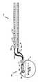
脊髄刺激は、或る特定の割合の患者の疼痛を緩和するための広く受け入れられた臨床的方法である。図1A及び図1Bに示されているように、SCSシステムは、典型的には、植え込み型パルス発生器(IPG)100を有し、このIPGは、例えばチタンで作られた生体適合性ケース30を有する。ケース30は、通常、IPGが機能するのに必要な回路及び電源又は電池を保持している。IPG100は、1本又は2本以上の電極リード(2つのかかるリード102,104が示されている)を介して電極106に結合されており、その結果、電極106は、電極アレイ110を形成するようになっている。電極106は、可撓性本体108で支持され、この可撓性本体は又、各電極に結合された個々の信号線112,114を収容している。信号線112,114は、インタフェース115によりIPG100に接続されており、このインタフェースは、リード102,104(又は図示していないリード延長部)をIPG100に取り外し可能に接続することができる任意の適当な装置であって良い。 Spinal cord stimulation is a widely accepted clinical method for alleviating pain in a certain percentage of patients. As shown in FIGS. 1A and 1B, an SCS system typically includes an implantable pulse generator (IPG) 100, which is a
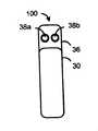
インタフェース115は、例えば、リード102,104に設けられたコネクタ119a,119bと対応関係をなして結合するよう構成されたリードコネクタ38a,38bを含む電気機械的コネクタ装置から成るのが良い。図示の実施形態では、リード102にE1 〜E8 と表示された8つの電極が存在し、リード104にはE9 〜E16 と表示された8つの電極が設けられているが、リード及び電極の数は特定用途向けであり、従って様々な場合がある。電極アレイ110は、典型的には、脊髄の硬膜に沿って植え込まれ、IPG100は、電極106を通って脊柱内の神経線維に送り出される電気パルスを発生させる。次に、IPG100それ自体が典型的には患者の臀部内で幾分遠くのところに植え込まれる。The
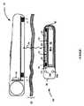
図2に示されているように、IPG100は、典型的には、プリント回路板(PCB)16を、このPCB16に取り付けられた種々の電子部品20、例えば、マイクロプロセッサ、集積回路及びキャパシタと一緒に含む電子基板組立体14を有する。最終的には、電子回路は、治療機能、例えば神経刺激を行う。フィードスルー(貫通接続)組立体24が、種々の電極信号を電子基板組立体14からリードコネクタ38a,38bに送り、これらリードコネクタは、リード102,104に結合されている(図1A及び図1B参照)。IPG100は、ヘッダコネクタ36を更に有し、このヘッダコネクタは、とりわけ、リードコネクタ38a,38bを収容している。IPG100は、ヘッダコネクタ36内に設けられていて、外部装置、例えば手持ち型又は臨床医用プログラマ(図示せず)に対してデータの送受を行うためのテレメトリ(遠隔計測)アンテナ又はコイル96(図1A)を更に有するのが良い。上述したように、IPG100は、通常、電源26、通常充電式電池26を更に有する。電源26は、外部充電器12によって経皮的に再充電可能である。具体的に説明すると、外部充電器12は、充電セッション中アクティブな状態にあるとき、その充電コイル17に通電し、充電コイル17は、IPG100内の充電コイル18中に電流を誘起させる。この誘起電流は、整流され、最終的には、患者の肉25を通って電源26を充電するために用いられる。 As shown in FIG. 2, the IPG 100 typically includes a printed circuit board (PCB) 16 together with various
典型的なIPG及びIPGシステムの構造及び機能に関するそれ以上の細部は、2005年12月14日に出願された米国特許出願第11/305,898号明細書に開示されており、この米国特許出願を参照により引用し、その開示内容を本明細書の一部とする。 Further details regarding the structure and function of a typical IPG and IPG system are disclosed in US patent application Ser. No. 11 / 305,898, filed Dec. 14, 2005, which is hereby incorporated by reference. Is hereby incorporated by reference and is incorporated herein by reference.
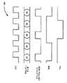
IPG100の内部に設けられた回路のための伝統的なアーキテクチャ50が図3に示されている。当業者であれば理解されるように、図3は、この開示により提供される要点を理解するのに十分に比較的高いレベルでIPG100の回路を示している。アーキテクチャ50は、IPG100内で種々の電気機能を実行する基本的な回路ブロックを有している。例えば、テレメトリ回路62がコイル96に結合されており、このテレメトリ回路は、データを外部コントローラ(図示せず)に対して送受するよう動作する。充電・電池保護回路64が同様に、充電コイル18に結合され、この充電・電池保護回路は、電源26と回路の残部との間に介在している。これら回路62,64の両方は、マイクロコントローラ60に結合され、このマイクロコントローラは、注目できるように、アーキテクチャ50の設計の中心である。電源投入時にマイクロコントローラ60により必要とされるプログラム及びデータは、シリアルインタフェース67によりマイクロコントローラ60に結合されたメモリ66、好ましくはシリアル不揮発性メモリに記憶されている。 A
予測可能な刺激療法を提供する際に関与する回路は、ディジタル集積回路(IC)70及びアナログIC80によって提供される。一用途では、ディジタルIC70は、刺激制御ロジック、例えば刺激パルス列に特定のタイミングを提供するようIPGのタイミングチャネルにより用いられる種々のタイマを備えている。アナログIC80は、シリアルリンクを介してディジタルIC70からデータを受け取り、かかるデータは、ディジタル‐アナログ変換器(DAC)82によりアナログ信号に変換され、このディジタル‐アナログ変換器は、最終的には、電極(E1...EN)に刺激をもたらす。加うるに、アナログIC80上に且つ充電ブロック64及びテレメトリブロック62内に生じ又はモニタされる種々のアナログ電圧、例えば種々の基準電圧、刺激コンプライアンス電圧等をマイクロコントローラ60に知らせるためにアナログ‐ディジタル(A/D)変換器74が用いられる。マイクロコントローラ60と一体のものとして示されているが、A/D変換器74は又、マイクロコントローラ60の外部に位置するディスクリート部品であっても良い。 The circuitry involved in providing predictable stimulation therapy is provided by a digital integrated circuit (IC) 70 and an
一実施形態では、マイクロコントローラ60、ディジタルIC70及びアナログIC80は、各々がIPGのプリント回路板16(図1参照)上の部品20のうちの1つから成るディスクリートICを構成する。アーキテクチャ50に含まれる他の機能ブロックは、他の部品20から成る場合があり、これら他の部品は、一体ではなく、少なくとも一部がディスクリート部品で形成される場合がある。 In one embodiment, the
アーキテクチャ50の機能ブロックを簡単に説明したが、注目されるべきこととして、これらブロックの詳細な動作を理解することは本発明にとって重要ではない。(読者は、機能ブロックの各々の一般的な知識を知りたい場合には、上記において引用した米国特許出願第11/305,898号明細書を参照するのが良い)。これとは異なり、理解すべき重要なことは、機能ブロックを相互に連結する仕方である。当業者であれば理解されるように、アーキテクチャ50の作用の中心はマイクロコントローラ60であり、このマイクロコントローラは、最終的には、あらゆる指令を他のブロックから受け取ったり、これらを他のブロックに送ったりする。さらに、注目できることとして、ブロック相互間の種々の相互連結は、形式及び複雑さが様々であり、連結方式の中には、性質上シリアルなものがあったり、単一のデータラインを有し、又は、データディジタルバスを有するものもある。さらに、ブロックのうちの幾つかは、他のブロックとの直接的接続関係を欠いており、それ故、中間ブロックにより互いに通信する必要がある。例えば、マイクロコントローラ60は、少なくとも一部が、ディジタルIC70を介してアナログIC80と通信する必要がある。 Although the functional blocks of
かかる相互接続性により、IPG100の出費及びその複雑さが増大する。さらに、かかる相互接続性は又、所望の変更及び(又は)新IPG改訂に合わせて特定のアーキテクチャを改造することを困難にする。例えば、機能ブロックのうちの1つを変更するには、他の機能ブロックにこれに対応した相当な変更が必要な場合があり、アップグレード又は改訂がコスト高になる。 Such interoperability increases the expense and complexity of the
加うるに、IPG100内のスペースは制限されている。というのは、IPGは、好ましくは、インプラントを患者にとって可能な限り影響がないようにするようできるだけ小形である。この点に関し、図3のアーキテクチャ50は、マイクロコントローラ60のために用いられる別個のIC、ディジタルIC70及びアナログIC80(場合によっては、他の部品)が必要なので一段と問題である。多くの部品を設けることにより、一般に、回路の信頼性がマイナスの影響を受けると共に電力消費量、一般に電力が制限されるIPGにとって大きな懸念が増大する。 In addition, space within the
本発明は、改良型IPGアーキテクチャにより植え込み型医療器具の分野において、この問題に対する解決策を提供する。 The present invention provides a solution to this problem in the field of implantable medical devices with an improved IPG architecture.
植え込み型医療器具、例えば植え込み型パルス発生器(IPG)の改良型アーキテクチャが開示される。一実施形態では、IPGのための機能ブロックが単一の集積回路(IC)に組み込まれる。機能ブロックの各々は、通信プロトコルにより制御される集中化バスを経て互いに通信すると共に必要ならば他のオフチップ(off-chip)装置と通信する。各回路ブロックは、バスと通信すると共に通信プロトコルに準拠するために、そのプロトコルに準拠したバスインタフェース回路を有する。各ブロックは、プロトコルに準拠しているので、任意所与のブロックを、他のブロックの設計に悪影響を及ぼさないで、容易に改造し又はアップグレードすることができ、それによりIPG回路のデバッキング及びアップグレーディングが容易になる。さらに、集中化バスを集積回路から外すことができるので、主要IPG用ICの主要な再設計を必要とすることなく、余分な回路をオフチップ状態で容易に追加してIPGを改造し又は機能をIPGに追加することができる。 An improved architecture of an implantable medical device, such as an implantable pulse generator (IPG), is disclosed. In one embodiment, functional blocks for the IPG are incorporated into a single integrated circuit (IC). Each of the functional blocks communicate with each other via a centralized bus controlled by a communication protocol and communicate with other off-chip devices if necessary. Each circuit block has a bus interface circuit conforming to the protocol in order to communicate with the bus and conform to the communication protocol. Since each block is compliant with the protocol, any given block can be easily modified or upgraded without adversely affecting the design of other blocks, thereby enabling IPG circuit debugging and Upgrade is easy. In addition, since the centralized bus can be removed from the integrated circuit, the IPG can be retrofitted or functioned easily by adding extra circuitry off-chip without requiring a major redesign of the primary IPG IC. Can be added to the IPG.
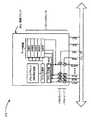
図4は、改良型IPGアーキテクチャ150の一例を示している。図3との比較によれば、図4の機能ブロックの大部分が図3の回路ブロックに対応しており、かくして、新規のアーキテクチャ150において同様な機能を実行することが示されている。しかしながら、改良型アーキテクチャ150内の機能ブロックの全ては、顕著な差として、集中化バス190に結合されている。本開示に示されている実施形態では、集中化バス190は、パラレルに動作する複数の多重化アドレス及びデータラインを有するパラレルバスである。しかしながら、これは厳密に言えば必要条件ではなく、その代わりに、バス190は、シリアルバスから成っていても良い。 FIG. 4 shows an example of an
好ましい実施形態では、図示の機能ブロックの各々は、単一の集積回路(IC)200内に組み込まれている。図示のようなIPG用IC200は、アナログ信号とディジタル信号の両方を含んでいるので、IC200は、混合モードチップから成る。しかしながら、厳密に言えば、アーキテクチャ150を図示のように単一のIC200上に実現することは必要条件ではない。さらに、理解されるべきこととして、IPG100内の或る特定の他の回路部品(例えば、データコイル96、充電コイル18、電源26及び外部メモリ66等)は、論理的にIC200の外部に位置する場合がある。よく言われるように、IPG内のできる限り多い機能ブロックをIC200上に統合することが依然として好ましい。というのは、このことは、歩留まりを増大させ、信頼性を高め、IPG内の電子回路のスペースを減少させ、IPG100内の回路の電力消費量を減少させたりその他のことをしたりするからである。 In the preferred embodiment, each of the illustrated functional blocks is incorporated within a single integrated circuit (IC) 200. Since the
改良型IPGアーキテクチャ150内の種々の機能ブロックの各々は、バスインタフェース回路215を介して集中化バス190と通信するが、これについては、後で詳細に説明する。好ましくは、機能ブロック相互間の他の全てのバスを利用しない通信は、最小限に保たれるが、幾つかのかかる通信は、有益である。例えば、図示のように、種々の割り込み(INT1,INT2,...)は、割り込みコントローラ173と直接通信し、それにより、集中化バス190を介するプロトコルを利用した通信に伴って生じる潜在的な遅延無く、種々の割り込みの発生を即座に認識できる。例えば、INT2は、電源26が危険レベルまで充電されたかどうかを割り込みコントローラ173に知らせることができ、その結果、IC200の動作を必要ならば一時的に停止させる場合がある。別のオフバス通信では、アナログバス192が種々のアナログ信号をA/Dブロック74に送るために利用され、A/Dブロックでは、かかる電圧をディジタル化することができ、そして必要に応じて集中化バス190を介して他の機能ブロックに利用可能にすることができる。 Each of the various functional blocks in the
機能ブロックの各々の動作原理を理解することは開示する改良型IPGアーキテクチャ150にとって重要ではないが、図4から注目すべきこととして、先行技術のディジタルIC70及びアナログIC80(図3)は、混合モード刺激回路ブロック175の状態に効果的に統合されており、これらの両方は、電極の各々Exのところで見える刺激パルスのタイミング、大きさ及び極性を設定する。 While understanding the operating principles of each of the functional blocks is not important to the disclosed
先行技術(図3)のアーキテクチャ50との別の重要な相違点として、集中化マイクロコントローラ60(図3)に代えて、内部コントローラ160が用いられていることに注目されたい。集中化バス190のパラレル化性状が与えられている場合、IC200内の制御は、1つのソースへの集中度が低く、その代わり、制御は、本質的には、コントローラ160と種々の機能ブロックとの間で分割され、コントローラ160は、「マスター」として働く。具体的に説明すると、各機能ブロックは、セットアップ及び状態レジスタ(図示せず)を有する。コントローラ160は、初期化の際、セットアップレジスタへの書き込みを行って各機能ブロックをコンフィグすると共にイネーブルにする。次に、状態レジスタは、各機能ブロックによって設定され、状態及び他の結果について問い合わせるためにコントローラ160によって読み取られる。マスターコントローラ160により課されるかかる制御とは別に、コントローラ160の外部に位置する機能ブロックの多くは、単純な状態機械を用いてこれらの動作を管理することができ、これら状態機械は、セットアップレジスタによりイネーブルにされると共に変更される。内部コントローラ160は、マスターとして働くので、内部コントローラ160のバスインタフェース回路215は、幾分ユニークであり、例えば、通信プロトコルによって用いられる制御信号(例えば、ALT、W/E及びR/E)のためのドライバ回路216を有し、このドライバ回路は、IC200内の他の機能ブロックのバスインタフェース回路215には欠けている。 Note that as another important difference from the prior art (FIG. 3)
図4で理解できるように、IC200は、例えば、電源26を接続し、コイル18,96を接続し、外部メモリ66を接続し、刺激電極を接続するのに必要な幾つかの外部端子202(例えば、ピン、ハンダバンプ等)を有する。好ましい実施形態では、他の外部端子202は、集中化バス190を構成する種々の信号にとって専用であり、それにより、この集中化バスは、IC200の外部に位置する他の装置と通信することができ、これについては以下に詳細に説明する。 As can be seen in FIG. 4, the
バス190を構成する種々の信号が図5に見え、この図5は、バス上で通信可能な考えられる1つのプロトコルを更に開示している。図示のように、集中化バス190は、同期化のためのクロック信号(CLK)、時分割多重化アドレス及びデータ信号(A/Dx)、アドレスバッチイネーブル信号(ALE)、アクティブロー(active-low)、書き込みイネーブル信号(*W/E)及びアクティブロー読み取りイネーブル信号(*R/E)から成っている。集中化バス90は、16のアドレス/データ信号を有するのが良いが、当然のことながら、この数は、システム要件に応じて変わるのが良い。The various signals making up the
当業者には理解されるように、例えば図4のIC200を含むIPGシステムにおける通信は、他のコンピュータ化システムと比較して比較的動作速度が遅い場合がある。これにより、集中化バス190上で用いられるプロトコルの要件が緩和され、比較的単純且つ比較的低速なプロトコルを用いることができる。例えば、クロック信号CLKに関する周波数は、32kHz〜1MHzであるのが良い。かかる周波数は、一般に、コンピュータ化プロトコルにとっては遅いが、典型的には数十マイクロ秒〜ミリ秒のオーダで刺激パルスを提供するIPGの動作と比較すると、適当に速い。 As will be appreciated by those skilled in the art, communication in an IPG system including, for example, the
図示されているように、プロトコルは、アドレスの次にそのアドレスに関する関連データが続く等するかなり単純なデータ前アドレス(address-before-data)方式を用いている。アドレスとデータの識別を助けるため、アドレスラッチイネーブル信号(ALE)は、アドレスの発行の際にのみアクティブであり、それにより、アドレスをクロック信号の立ち上がり端の際にラッチすることができる。特定のアドレスに対応したデータが書き込まれるか読み取られるかは、書き込み及び読み取りイネーブル信号(*W/E、*R/E)のアサート(真)で決まる。当然のことながら、このプロトコルは、例示に過ぎず、他のプロトコル及びフォーマットを集中化バス190上での通信のために使用できる。As shown, the protocol uses a fairly simple address-before-data scheme, such as an address followed by associated data for that address. To help identify the address and data, the address latch enable signal (ALE) is only active when the address is issued, so that the address can be latched on the rising edge of the clock signal. Whether data corresponding to a specific address is written or read is determined by assertion (true) of a write and read enable signal (* W / E,* R / E). Of course, this protocol is exemplary only, and other protocols and formats can be used for communication on the
図5のプロトコルの性状は、集中化バス190に結合された全ての機能ブロックをアドレスと呼ばなければならず、恐らくは、或る範囲のアドレスと呼ばなければならないことを意味している。例えば、コンプライアンス電圧のための値を保持するデータレジスタのためのアドレス(A/Dブロック74において)は、ADDR[3401]であり、バンドギャップ基準電圧のためのアドレスは、ADDR[3402]であり、電極E6によって提供されるべき刺激の大きさのためのアドレス(刺激回路ブロック175において)は、ADDR[7655]であり、他方、そのパルスの持続時間は、ADDR[7656]で記憶されるのが良く、その他同様である。 The nature of the protocol of FIG. 5 means that all functional blocks coupled to the
関連アドレスを認識する際に種々の機能ブロックを助けるため且つ集中化バス190のプロトコルに従って機能する各ブロックの能力を保証するため、各ブロックは、図6に示されているバスインタフェース回路215を有している。当業者であればバスインタフェース回路215の動作原理を良く理解しており、したがって、これを一般的なレベルで説明する。上述したように、1つ又は2つ以上のアドレス、例えば図6の単純な例では、ADDR[1]〜[5]は、各機能ブロックと関連している場合がある。かかるアドレスが種々のブロックのところで受け取られると、各ブロックは、これらアドレスを復号して突き合わせ(マッチ)を判定し、即ち、このアドレスがそのブロックを示すアドレスのうちの1つに対応しているかどうかを判定する。もしそうであれば、データが問題のアドレスに書き込まれ又はこれから読み取られるかどうかに応じて、バスドライバ(読み取りの場合)又はバスレシーバ(書き込みの場合)は、イネーブルにされ、次にデータがブロックのデータレジスタに書き込まれ又はこれから読み取られる。このプロトコルに準拠するため、ブロック内の実際の機能回路(図6には示されていない)は、当業者には理解されるように、データレジスタンスと適切にインタフェースをとる必要がある。 Each block has a
バスインタフェース回路215により、各機能ブロックがバス190について確立されたプロトコルを用いて通信することができる状態では、種々の機能ブロックに変更を加えて回路の誤差を修正すると共に(或いは)次世代IPGで使用可能にIC200をアップグレードすることは、今や、比較的簡単なことになる。これは、ブロックの回路の各々を変更でき、この場合、かかる変更が関連のブロックの他の変化を必要とし又は他のブロックの動作を動揺させるという心配が無いからである。機能ブロックを別個独立に設計し、パラレルに検証することができ、それにより、設計プロセス中における時間及び労力を節約することができる。 While the
改良型アーキテクチャ150のもう1つの利点は、IC200の外部に位置するIPG100を容易に改造し又は機能をこれに追加することができるということにある。例えば、将来における改良では、IPGは、もしそうでない場合にオンチップメモリ177又はオフチップメモリ66(図4参照)で記憶できるデータよりもより多くのデータを記憶することが必要な場合がある。かかる場合、集中化バスアーキテクチャ150がIC200内で用いられている場合、バス190を図7に示されているようにIC200の外部に延長することができ、そしてメモリ300(好ましくは、不揮発性メモリ)を追加することができる。これは、非常に有利であり、その理由は、これにより、IC200及び(又は)その機能ブロックのうちの幾つかを再設計する必要なく、IPG回路をアップグレードすることができるからである。 Another advantage of the
開示したアーキテクチャ150がどのようにシステム統合のためになるかを示す別の例では、システムの容量を第1のIC200と同様に構成された別のIC200′ の追加によって効果的に2倍にすることができる。これにより、IC200,200′ が収納されたIPG100は、32個の刺激電極、即ち、ICの両方から各々16個ずつの刺激電極を提供することができる。換言すると、IPGの容量を複数の刺激ICを互いに単純に「デイジィチェイニング(daisy chaining)」することにより増大させることができる。かかる実施形態では、IC200又はIC200′ のうちの一方の内部コントローラ160をイナクティブな状態にしてコントローラ160が1つしかシステムのマスターコントローラとして働かないようにすることが有益な場合がある。変形例として、IPGシステムは、IC200,200′ の両方のコントローラ160を利用しても良い。ただし、これには、潜在的なコンフリクト、即ち、図8〜図10を参照して以下に説明する課題を解決するための2つのコントローラ相互間におけるアービトレーションが必要である。 In another example showing how the disclosed
また、バス190によりIC200の外部に他の装置を追加することができる。例えば、アーキテクチャ150の使用によりイネーブルにされる1つの特に関心のある用途は、少なくとも或る程度の系統的制御をIC200の外部に配置することができるということにある。例えば、図7では、外部マイクロコントローラ240がIC200内に位置する内部コントローラ160に取って代わり又はこれを補うために用いられる(外部マイクロコントローラ240は、上述の要点である追加のIC200′ の内部コントローラ160から成っていても良い)。この場合も又、外部コントローラによりIPGを制御できるということは、IC200又は種々の機能ブロックに変更を加えないでIPGのためのプログラミングを変更できるということを意味している。 Further, another device can be added outside the
しかしながら、外部マイクロコントローラ240により追加の制御を提供するためには、2つの制御機構相互間にコンフリクトが無いようにするために内部コントローラ160と外部マイクロコントローラ240との間に追加の通信手段が必要な場合がある。図8〜図10は、内部コントローラ160と外部マイクロコントローラ240がコンフリクト無くIC200の制御をどのように分担することができるかを記載している。 However, in order to provide additional control by the
外部制御の可能性の認識に当たり、内部コントローラ160は、図8及び図9に示されているように追加の機能を備えている。素早くプレビューすることにより、この追加の機能は、バス190上に出された特定の指令が内部コントローラ160によって取り扱われるべきか外部マイクロコントローラ240によって取り扱われるべきかどうかを認識するよう設計されている。どちらの装置160又は240が最終的に問題になっている指令を処理するかは、コントローラ選択ビット(CSB)によって設定される。CSB=0である場合、内部コントローラ160が問題の指令を実行し、CSB=1であれば、外部マイクロコントローラ240がその指令を実行する。図7及び図9で理解できるように、CSBは、全体として集中化バス190の範囲の外部に位置するディスクリート通信信号を構成することができ、このディスクリート通信信号は、その離散的性格により、2つのコントローラ160,240相互間の迅速且つ安全なアービトレーション方法として好ましい具体化例であることが可能である。他の具体化例では、コントローラ選択ビットは、バス190のプロトコルを用いてバス190を介して送られるデータを構成することができる。かかる具体化例では、CSBデータは、バス190により内部コントローラ160と外部マイクロコントローラ240との間で受け渡しされる制御「送信許可証(トークン)」と見なすことができる。コントローラ相互間におけるかかる純粋にバスを利用するアービトレーション方法は、容易に具体化される。しかしながら、バスを利用しないディスクリート信号方式を用いて2つのコントローラ160.240相互間の制御の受け渡しを説明することが容易なので、この方式は、以下に説明されると共に図示されている。 In recognizing the possibility of external control, the internal controller 160 has an additional function as shown in FIGS. By quickly previewing, this additional functionality is designed to recognize whether a particular command issued on
図示のように、内部コントローラ160は、図8に詳細に示された2つのレジスタ、即ち、指令レジスタ220及び指令オーナレジスタ230を備えた状態で設計されている。指令レジスタ220は、多くのコントローラの標準的な特徴であり、単純に、IPGが実行することができる種々の指令の二値表示から成る。図示の例では、指令レジスタ220は、長さが8ビットなので、IPG100は、256(28 )の互いに異なる指令を処理することができる。指令オーナレジスタ230は、関連の指令(この例では、256)が存在するので同数のビットで構成され、レジスタ内の各ビットは、特定の指令が内部コントローラ160によって取り扱われるべきであるか外部マイクロコントローラ240によって取り扱われるべきであるかどうかを示している。図示のように、指令オーナレジスタ230内の特定のビットが“0”である場合、対応の指令は、内部コントローラ160によって実行されることになり、“1”であれば、外部マイクロコントローラ240が、その指令を実行することになる。単純な例では、256ビット指令オーナレジスタ230が、“1010000...0001”を読み取った場合、指令256,254,1(CMD256,CMD254,CMD1)は、外部マイクロコントローラ240によって実行され、他の全ての指令は、内部コントローラ160によって実行される。As shown, the internal controller 160 is designed with two registers shown in detail in FIG. 8, namely a command register 220 and a
コントローラ選択ビット(CSB)245を送出するための指令レジスタ220及び指令オーナレジスタ230の使用法が図9に示されている。指令が指令レジスタ220によっていったん受け取られると、指令は復号されて(例えば、多重分離されて)その指令番号(CMD256〜CMD1)が理解される。次に、指令番号を用いて適当な指令オーナビットを指令オーナレジスタ230から取り出す。このビットをコントローラ選択ビット(CSB)245として設定してどのコントローラ(160,240)が指令を上述したように取り扱うべきであるかどうかを指示する。 The use of command register 220 and
このプロセスについて図10を参照して詳細に説明する。起動時、指令オーナレジスタ230にメモリ(内部メモリ177、シリアル外部メモリ66等)からデフォルト値をロードする。通常、指令オーナレジスタ230内の種々の指令オーナビットのデフォルト値は、全て“0”であり、このことは、少なくとも最初の全ての指令が内部コントローラ160によって実行されるべきことを示している。しかる後、動作中の或る時点で、指令レジスタ220にそのアドレス(ADDR[CMD])で指令をロードする。指令を上述したように復号し(多重分離し)、対応の指令オーナビットをコントローラ選択ビット(CSB)245として送出する。また、CSB245を図9に示されているようにそのアドレス(ADDR[CER])(これは、単一ビットから成るのが良い)でコントローライネーブルレジスタ250に記憶させる。また、CSB245を外部マイクロコントローラ240に送る。 This process will be described in detail with reference to FIG. At startup, the
CSB245が送出されると、今や、コントローラ160又は240のうちのどちらが問題の指令を実行するかどうかが分かり、かくして、それに応じて種々の措置を取る。CSB=“0”であって内部コントローラ160が示されている場合、そのコントローラ160がその指令を実行することを除き、達成されることが必要なことは殆ど無い。デフォルトとして、外部マイクロコントローラ240が内部コントローラ160による指令の実行とコンフリクトしないようにするため、外部コントローラ240に書き込まれたアービトレーション論理246は、CSB=0であることを検出すると、外部コントローラのバスドライバ242をディスエーブルにする(無効にする)。これとは対照的に、記憶されたコントローライネーブルレジスタビット250(アクティブロー信号)により内部コントローラバスドライバ212をイネーブルにする(有効にする)。内部コントローラ160がその指令を実行した後、システムは、次の指令を待ち、上述の方法が繰り返され、以下同様である。 When the
しかしながらCSB=“1”であり、外部マイクロコントローラ240が示されている場合、制御を一時的に外部マイクロコントローラ240にシフトすることができる余分のステップを実行する。具体的に説明すると、外部マイクロコントローラ内のアービトレーション論理246は、CSB=“1”であることの検出時に、これが制御中であることを認識し、そのバスドライバ242をイネーブルにする。これとは対照的に、内部コントローラバスドライバ212をディスエーブルにする。加うるに、CSB=“1”であることを認識すると、アービトレーション論理246は、バス190を介して指令レジスタ220のアドレス(ADDR[CMD])からの読み取りを要求することによりそのレジスタ220に記憶されている指令(即ち、その指令)を取り出す。外部マイクロコントローラ240は、その指令をいったん受け取ると、その指令を実行する。 However, if CSB = “1” and the
その指令が外部マイクロコントローラ240によって実行されると、図10に示されている残りのステップを次の指令の受け取りに先立つ内部コントローラ160への制御の戻しに差し向ける。指令の実行後、アービトレーション論理246は、今や、“0”をコントローライネーブルレジスタ250に書き込み、このコントローライネーブルレジスタは、バス190によりそのアドレスADDR[CER]でアクセス可能である。これにより、もう一度、内部コントローラ160のためのバスドライバ212がイネーブルになる。コントローライネーブルレジスタ250の上書きと同時に、アービトレーション論理246により、外部コントローラ240のためのバスドライバ242がディスエーブルになる。これにより、システムは内部コントローラ160がデフォルトによって制御を引き受けるその初期状態に復元し、その時点において、システムは、その次の指令を待ち、上述の方法が繰り返され、その他同様である。 When that command is executed by
図10の流れは、内部及び外部コントローラ160,240が改良型集中化バスアーキテクチャ150に従ってコンフリクト無しに一緒に動作することができるようにするまさに一手法である。しかしながら、当業者であれば認識されるように、この同じ目的を達成する他の流れ及び他の回路が可能であり、従って、図示の内容は、単なる一例として理解されるべきである。 The flow of FIG. 10 is just one way to allow the internal and
本発明の特定の実施形態を図示すると共に説明したが、上述の説明は、本発明をこれら実施形態に限定するものではないことは理解されるべきである。当業者にとっては明らかなように、本発明の精神及び範囲から逸脱することなく種々の変更及び改造を実施できる。かくして、本発明は、特許請求の範囲に記載された本発明の精神及び範囲に属する変形例、改造例及び均等例を含むものである。 While particular embodiments of the present invention have been illustrated and described, it is to be understood that the above description is not intended to limit the invention to these embodiments. It will be apparent to those skilled in the art that various modifications and variations can be made without departing from the spirit and scope of the invention. Thus, the present invention includes modifications, alterations and equivalents belonging to the spirit and scope of the present invention as defined in the claims.
本発明に関する上記の教示を考慮に入れるならば、本発明の種々の変更が可能であることは明白である。本発明は、特許請求の範囲において特定したものとは異なる態様で実施することも可能である。 Obviously, various modifications of the present invention are possible in light of the above teachings. The invention may be practiced otherwise than as specified in the claims.
本発明に関連する好ましい態様として、例えば、以下のものをあげることができる。
〔態様1〕
植え込み型刺激器具であって、
各々が前記植え込み型医療器具内で少なくとも1つの機能を実行する複数の機能ブロックを備えた集積回路を有し、少なくとも1つの他の機能ブロックは、前記植え込み型刺激器具のための刺激回路を有し、少なくとも1つの組織刺激電極が、前記刺激回路に結合されており、
前記機能ブロックの各々と通信状態にあるバスを有し、前記機能ブロックは、バスプロトコルを経て互いに通信する、器具。
〔態様2〕
前記機能ブロックのうちの1つは、マスターコントローラから成り、他の全ての機能ブロックは、前記マスターコントローラのスレーブである、上記態様1に記載の器具。
〔態様3〕
前記機能ブロックのうちの1つは、アナログ‐ディジタル変換器から成り、前記アナログ‐ディジタル変換器は、前記バスの外部に位置する前記機能ブロックのうちの少なくとも幾つかから複数のアナログ信号を受け取る、上記態様1に記載の器具。
〔態様4〕
前記集積回路は、外部端子を有し、前記バスは、前記バスが前記集積回路の外部に位置する少なくとも1つの装置と通信することができるよう少なくとも1つの外部端子と通信する、上記態様1に記載の器具。
〔態様5〕
前記装置は、メモリ回路から成る、上記態様4に記載の器具。
〔態様6〕
前記装置は、コントローラから成る、上記態様4に記載の器具。
〔態様7〕
前記機能ブロックのうちの少なくとも幾つかは、他の機能ブロックに割り込みをかけ、前記割り込みは、前記バス上を移動することはない、上記態様1に記載の器具。Examples of preferred embodiments related to the present invention include the following.
[Aspect 1]
An implantable stimulator,
Each has an integrated circuit with a plurality of functional blocks that perform at least one function within the implantable medical device, and at least one other functional block has a stimulation circuit for the implantable stimulation device. And at least one tissue stimulation electrode is coupled to the stimulation circuit;
An instrument having a bus in communication with each of the functional blocks, the functional blocks communicating with each other via a bus protocol.
[Aspect 2]
The instrument of
[Aspect 3]
One of the functional blocks comprises an analog-to-digital converter, wherein the analog-to-digital converter receives a plurality of analog signals from at least some of the functional blocks located outside the bus; The instrument according to
[Aspect 4]
In
[Aspect 5]
The apparatus of claim 4, wherein the device comprises a memory circuit.
[Aspect 6]
The instrument of claim 4, wherein the device comprises a controller.
[Aspect 7]
The apparatus of
〔態様8〕
植え込み型刺激器具であって、
各々が前記植え込み型医療器具内で少なくとも1つの機能を実行する複数の機能ブロックを有し、少なくとも1つの他の機能ブロックは、前記植え込み型刺激器具のための刺激回路を有し、少なくとも1つの組織刺激電極が、前記刺激回路に結合されており、
前記機能ブロックの各々と通信状態にあるパラレルバスを有し、前記機能ブロックは、バスプロトコルを経て互いに通信する、器具。
〔態様9〕
前記機能ブロックのうちの1つは、マスターコントローラから成り、他の全ての機能ブロックは、前記マスターコントローラのスレーブである、上記態様8に記載の器具。
〔態様10〕
前記機能ブロックのうちの1つは、アナログ‐ディジタル変換器から成り、前記アナログ‐ディジタル変換器は、前記バスの外部に位置する前記機能ブロックのうちの少なくとも幾つかから複数のアナログ信号を受け取る、上記態様8に記載の器具。
〔態様11〕
前記複数の機能ブロック及び前記バスは、単一の集積回路上に集積され、前記集積回路は、外部端子を有し、前記バスは、前記バスが前記集積回路の外部に位置する少なくとも1つの装置と通信することができるよう少なくとも1つの外部端子と通信する、上記態様8に記載の器具。
〔態様12〕
前記装置は、メモリ回路から成る、請求項11記載の器具。
〔態様13〕
前記装置は、コントローラから成る、請求項11記載の器具。
〔態様14〕
前記機能ブロックのうちの少なくとも幾つかは、他の機能ブロックに割り込みをかけ、前記割り込みは、前記バス上を移動することはない、上記態様8に記載の器具。[Aspect 8]
An implantable stimulator,
Each having a plurality of functional blocks that perform at least one function within the implantable medical device, at least one other functional block having a stimulation circuit for the implantable stimulation device, and at least one A tissue stimulation electrode is coupled to the stimulation circuit;
An instrument having a parallel bus in communication with each of the functional blocks, the functional blocks communicating with each other via a bus protocol.
[Aspect 9]
The apparatus of aspect 8, wherein one of the functional blocks comprises a master controller and all other functional blocks are slaves of the master controller.
[Aspect 10]
One of the functional blocks comprises an analog-to-digital converter, wherein the analog-to-digital converter receives a plurality of analog signals from at least some of the functional blocks located outside the bus; The instrument according to aspect 8 above.
[Aspect 11]
The plurality of functional blocks and the bus are integrated on a single integrated circuit, the integrated circuit has an external terminal, and the bus is at least one device in which the bus is located outside the integrated circuit. 9. The instrument of aspect 8, wherein the instrument is in communication with at least one external terminal so that it can communicate with.
[Aspect 12]
The instrument of claim 11, wherein the device comprises a memory circuit.
[Aspect 13]
The instrument of claim 11, wherein the device comprises a controller.
[Aspect 14]
9. The apparatus of aspect 8, wherein at least some of the functional blocks interrupt other functional blocks, and the interrupt does not travel on the bus.
〔態様15〕
植え込み型刺激器具であって、
各々が前記植え込み型医療器具内で少なくとも1つの機能を実行する複数の機能ブロックを有し、少なくとも1つの他の機能ブロックは、前記植え込み型刺激器具のための刺激回路を有し、少なくとも1つの組織刺激電極が、前記刺激回路に結合されており、
前記機能ブロックの各々と通信状態にあるパラレルバスを有し、
各機能ブロックと前記バスとの間に介在して設けられたバスインタフェース回路を有し、前記バスインタフェース回路により、各ブロックは、プロトコルに従って前記バスを経て他の機能ブロックと通信することができる、器具。
〔態様16〕
前記機能ブロックのうちの1つは、マスターコントローラから成り、他の全ての機能ブロックは、前記マスターコントローラのスレーブである、上記態様15に記載の器具。
〔態様17〕
前記機能ブロックのうちの1つは、アナログ‐ディジタル変換器から成り、前記アナログ‐ディジタル変換器は、前記バスの外部に位置する前記機能ブロックのうちの少なくとも幾つかから複数のアナログ信号を受け取る、上記態様15に記載の器具。
〔態様18〕
前記複数の機能ブロック、前記バス、及び前記バスインタフェース回路は、単一の集積回路上に集積されている、上記態様15に記載の器具。
〔態様19〕
前記集積回路は、外部端子を有し、前記バスは、前記バスが前記集積回路の外部に位置する少なくとも1つの装置と通信することができるよう少なくとも1つの外部端子と通信する、上記態様18に記載の器具。
〔態様20〕
前記装置は、メモリ回路から成る、上記態様19に記載の器具。
〔態様21〕
前記装置は、コントローラから成る、上記態様19に記載の器具。
〔態様22〕
前記機能ブロックのうちの少なくとも幾つかは、他の機能ブロックに割り込みをかけ、前記割り込みは、前記バス上を移動することはない、上記態様15に記載の器具。[Aspect 15]
An implantable stimulator,
Each having a plurality of functional blocks that perform at least one function within the implantable medical device, at least one other functional block having a stimulation circuit for the implantable stimulation device, and at least one A tissue stimulation electrode is coupled to the stimulation circuit;
Having a parallel bus in communication with each of the functional blocks;
It has a bus interface circuit provided between each functional block and the bus, and by the bus interface circuit, each block can communicate with other functional blocks via the bus according to a protocol. Instruments.
[Aspect 16]
16. The instrument of aspect 15, wherein one of the functional blocks consists of a master controller and all the other functional blocks are slaves of the master controller.
[Aspect 17]
One of the functional blocks comprises an analog-to-digital converter, wherein the analog-to-digital converter receives a plurality of analog signals from at least some of the functional blocks located outside the bus; The instrument according to aspect 15 above.
[Aspect 18]
16. The instrument according to aspect 15, wherein the plurality of functional blocks, the bus, and the bus interface circuit are integrated on a single integrated circuit.
[Aspect 19]
In
[Aspect 20]
The apparatus of embodiment 19, wherein the device comprises a memory circuit.
[Aspect 21]
The apparatus of aspect 19, wherein the device comprises a controller.
[Aspect 22]
16. The apparatus of aspect 15, wherein at least some of the functional blocks interrupt other functional blocks, and the interrupt does not travel on the bus.
〔態様23〕
植え込み型刺激器具であって、
各々が前記植え込み型医療器具内で少なくとも1つの機能を実行する複数の機能ブロックを備えた集積回路を有し、少なくとも1つの他の機能ブロックは、前記植え込み型刺激器具のための刺激回路を有し、少なくとも1つの組織刺激電極が、前記刺激回路に結合されており、
前記集積回路の外部に位置する少なくとも1つの装置を有し、
前記機能ブロックの各々及び前記外部装置と通信状態にあるバスを有し、前記外部装置及び前記機能ブロックは、プロトコルに従って前記バスと通信する、器具。
〔態様24〕
前記機能ブロックのうちの1つは、マスターコントローラから成り、他の全ての機能ブロックは、前記マスターコントローラのスレーブである、上記態様23に記載の器具。
〔態様25〕
前記機能ブロックのうちの1つは、アナログ‐ディジタル変換器から成り、前記アナログ‐ディジタル変換器は、前記バスの外部で複数のアナログ信号を受け取る、上記態様23に記載の器具。
〔態様26〕
前記集積回路は、外部端子を有し、前記バス中の各信号は、前記バスが前記集積回路の外部に位置する少なくとも1つの装置と通信することができるよう外部端子と通信する、上記態様23に記載の器具。[Aspect 23]
An implantable stimulator,
Each has an integrated circuit with a plurality of functional blocks that perform at least one function within the implantable medical device, and at least one other functional block has a stimulation circuit for the implantable stimulation device. And at least one tissue stimulation electrode is coupled to the stimulation circuit;
Having at least one device located external to the integrated circuit;
An instrument having a bus in communication with each of the functional blocks and the external device, wherein the external device and the functional block communicate with the bus according to a protocol.
[Aspect 24]
The apparatus of aspect 23, wherein one of the functional blocks comprises a master controller and all other functional blocks are slaves of the master controller.
[Aspect 25]
24. The apparatus of aspect 23, wherein one of the functional blocks comprises an analog-to-digital converter, the analog-to-digital converter receiving a plurality of analog signals outside the bus.
[Aspect 26]
The aspect 23, wherein the integrated circuit has an external terminal, and each signal in the bus communicates with an external terminal so that the bus can communicate with at least one device located outside the integrated circuit. The instrument described in 1.
〔態様27〕
植え込み型医療器具であって、
各々が前記植え込み型医療器具内で少なくとも1つの機能を実行する複数の機能ブロックを有し、少なくとも2つのブロックは、他の機能ブロックのための第1のコントローラを有し、
前記機能ブロックのうちの少なくとも幾つかを制御することができる第2のコントローラを有し、
前記機能ブロックの各々及び前記第2のコントローラと通信状態にあるバスを有し、
前記第1のコントローラと前記第2のコントローラは、他の機能ブロックの制御を分担する、器具。
〔態様28〕
前記植え込み型医療器具は、植え込み型刺激器である、上記態様27に記載の器具。
〔態様29〕
前記他の機能ブロックのうちの少なくとも1つは、電気刺激を患者の組織に送り出す少なくとも1つの電極に結合された刺激回路から成る、上記態様28に記載の器具。
〔態様30〕
前記第1のコントローラを含む前記機能ブロックは、集積回路中に集積され、前記第2のコントローラは、前記集積回路の外部に位置する、上記態様27に記載の器具。[Aspect 27]
An implantable medical device,
Each having a plurality of functional blocks that perform at least one function within the implantable medical device, the at least two blocks having a first controller for the other functional blocks;
A second controller capable of controlling at least some of the functional blocks;
A bus in communication with each of the functional blocks and the second controller;
The instrument in which the first controller and the second controller share control of other functional blocks.
[Aspect 28]
The device according to aspect 27, wherein the implantable medical device is an implantable stimulator.
[Aspect 29]
29. The apparatus of aspect 28, wherein at least one of the other functional blocks comprises a stimulation circuit coupled to at least one electrode that delivers electrical stimulation to patient tissue.
[Aspect 30]
28. The apparatus according to aspect 27, wherein the functional block including the first controller is integrated in an integrated circuit, and the second controller is located outside the integrated circuit.
〔態様31〕
植え込み型医療器具であって、
各々が前記植え込み型医療器具内で少なくとも1つの機能を実行する複数の機能ブロックを備えた集積回路を有し、少なくとも1つのブロックは、前記集積回路内の他の機能ブロックのための内部コントローラから成り、
前記集積回路の外部に位置する外部コントローラ装置を有し、
前記機能ブロックの各々及び前記外部コントローラと通信状態にあるバスを有し、
前記バス上の少なくとも1つの第1の指令は、前記内部コントローラにより実行可能であり、前記バス上の少なくとも1つの第2の指令は、前記外部コントローラによって実行可能である、器具。
〔態様32〕
前記植え込み型医療器具は、植え込み型刺激器である、上記態様31に記載の器具。
〔態様33〕
前記他の機能ブロックのうちの少なくとも1つは、電気刺激を患者の組織に送り出す少なくとも1つの電極に結合された刺激回路から成る、上記態様32に記載の器具。
〔態様34〕
前記内部コントローラは、出された指令が前記内部コントローラにより実行可能な第1の指令を含むか前記外部コントローラによって実行可能な第2の指令を含むかを判定する回路を有する、上記態様31に記載の器具。
〔態様35〕
前記回路は、前記出された指令を第1の指令か第2の指令かのいずれかとして指定するビットのレジスタを有する、上記態様34に記載の器具。
〔態様36〕
前記回路は、コントローラ選択ビットを、前記外部コントローラ中のアービトレーション回路に送出する、上記態様35に記載の器具。[Aspect 31]
An implantable medical device,
Each having an integrated circuit with a plurality of functional blocks that perform at least one function in the implantable medical device, the at least one block from an internal controller for other functional blocks in the integrated circuit Consisting of
An external controller device located outside the integrated circuit;
Having a bus in communication with each of the functional blocks and the external controller;
An instrument wherein at least one first command on the bus is executable by the internal controller and at least one second command on the bus is executable by the external controller.
[Aspect 32]
The device according to aspect 31, wherein the implantable medical device is an implantable stimulator.
[Aspect 33]
35. The apparatus of aspect 32, wherein at least one of the other functional blocks comprises a stimulation circuit coupled to at least one electrode that delivers electrical stimulation to patient tissue.
[Aspect 34]
The internal controller has a circuit for determining whether the issued command includes a first command executable by the internal controller or a second command executable by the external controller. Appliances.
[Aspect 35]
35. The apparatus of aspect 34, wherein the circuit comprises a register of bits that specifies the issued command as either a first command or a second command.
[Aspect 36]
36. The apparatus of aspect 35, wherein the circuit sends a controller selection bit to an arbitration circuit in the external controller.
〔態様37〕
植え込み型刺激器具を作動させる方法であって、
機能ブロックをバスに結合するステップを有し、前記機能ブロックのうちの1つは、第1のコントローラから成り、少なくとも1つの他の機能ブロックは、前記植え込み型刺激器具のための刺激回路から成り、少なくとも1つの組織刺激電極が、電気刺激回路に結合され、
第2のコントローラを前記バスに結合するステップを有し、
指令を前記バス上に送出するステップを有し、
前記指令が前記第1のコントローラによって実行されるべきであるか前記第2のコントローラによって実行されるべきであるかを判定し、前記指令をそれに応じて実行するステップを有する、方法。
〔態様38〕
前記機能ブロックは、集積回路上に集積され、前記第2のコントローラは、前記集積回路の外部に位置する、上記態様37に記載の方法。
〔態様39〕
前記判定ステップは、前記指令を復号し、前記第1のコントローラ中の関連のオーナビットに問い合わせることにより前記第1のコントローラによって実施される、上記態様37に記載の方法。
〔態様40〕
前記指令が前記第2のコントローラによって実行される場合、信号を前記第2のコントローラに送るステップを更に有し、前記第2のコントローラは、前記第1のコントローラから前記指令を取り出して前記取り出した指令を実行する、上記態様39に記載の方法。〔態様41〕
前記第2のコントローラによる前記取り出した指令の実行後、制御を前記第1のコントローラに戻すステップを更に有する、上記態様40に記載の方法。[Aspect 37]
A method of operating an implantable stimulator comprising:
Coupling functional blocks to a bus, wherein one of the functional blocks comprises a first controller and at least one other functional block comprises a stimulation circuit for the implantable stimulation device. At least one tissue stimulation electrode is coupled to the electrical stimulation circuit;
Coupling a second controller to the bus;
Sending instructions on the bus;
Determining whether the command is to be executed by the first controller or the second controller and executing the command accordingly.
[Aspect 38]
38. The method of aspect 37, wherein the functional block is integrated on an integrated circuit, and the second controller is located outside the integrated circuit.
[Aspect 39]
38. The method of aspect 37, wherein the determining step is performed by the first controller by decoding the command and querying an associated owner bit in the first controller.
[Aspect 40]
If the command is executed by the second controller, the method further comprises a step of sending a signal to the second controller, wherein the second controller retrieves the command from the first controller and retrieves the command. 40. The method of aspect 39, wherein the command is executed. [Aspect 41]
41. The method of aspect 40, further comprising returning control to the first controller after execution of the retrieved command by the second controller.
Claims (16)
Translated fromJapanese複数の機能ブロックを有する集積回路を備え、
前記機能ブロックは、
1つ以上の(i)アナログ‐ディジタル変換器、(ii)植え込み型刺激器具の外部に位置する装置と通信するように構成された遠隔測定回路、または、(iii)植え込み型刺激器具の電池を充電するように構成された電池充電回路を有しており、
前記機能ブロックは、さらに、植え込み型刺激器具の刺激回路を有し、
少なくとも1つの組織刺激電極が、前記刺激回路に結合されており、
前記機能ブロックは、さらに、前記1つ以上の機能ブロックによって発生された割り込みを受け入れるように構成された割り込みコントローラを有し、
前記植え込み型刺激器具は、さらに、前記機能ブロックの各々に直接結合されたバスを備え、
前記機能ブロックは、バスプロトコルを経て互いに通信するようになっており、
前記割り込みは、前記バスで通信しないようになっている、
ことを特徴とする器具。An implantable stimulator,
An integrated circuit having a plurality of functional blocks;
The functional block is
One or more (i) an analog-to-digital converter, (ii) a telemetry circuit configured to communicate with a device located external to the implantable stimulator, or (iii) a battery of the implantable stimulator A battery charging circuit configured to charge;
The functional block further includes a stimulation circuit for an implantable stimulation device,
At least one tissue stimulation electrode is coupled to the stimulation circuit;
The functional block further comprises an interrupt controller configured to accept interrupts generated by the one or more functional blocks;
The implantable stimulator further comprises a bath directly coupled to each of the functional blocks;
The functional blocks communicate with each other via a bus protocol,
The interrupt does not communicate on the bus,
A device characterized by that.
複数の機能ブロックを備え、
前記機能ブロックは、
1つ以上の(i)アナログ‐ディジタル変換器、(ii)植え込み型刺激器具の外部に位置する装置と通信するように構成された遠隔測定回路、または、(iii)植え込み型刺激器具の電池を充電するように構成された電池充電回路を有しており、
前記機能ブロックは、さらに、植え込み型刺激器具の刺激回路を有し、
少なくとも1つの組織刺激電極が、前記刺激回路に結合されており、
前記機能ブロックは、さらに、前記1つ以上の機能ブロックによって発生された割り込みを受け入れるように構成された割り込みコントローラを有し、
前記植え込み型刺激器具は、さらに、前記機能ブロックの各々に直接結合されたバスを備え、
前記バスの通信は、バスプロトコルを介して制御されるようになっており、
前記割り込みは、前記バスで通信しないようになっている、
ことを特徴とする器具。An implantable stimulator,
With multiple functional blocks,
The functional block is
One or more (i) an analog-to-digital converter, (ii) a telemetry circuit configured to communicate with a device located external to the implantable stimulator, or (iii) a battery of the implantable stimulator A battery charging circuit configured to charge;
The functional block further includes a stimulation circuit for an implantable stimulation device,
At least one tissue stimulation electrode is coupled to the stimulation circuit;
The functional block further comprises an interrupt controller configured to accept interrupts generated by the one or more functional blocks;
The implantable stimulator further comprises a bath directly coupled to each of the functional blocks;
The bus communication is controlled via a bus protocol,
The interrupt does not communicate on the bus,
A device characterized by that.
複数の機能ブロックを有する集積回路を備え、
前記機能ブロックは、
1つ以上の(i)アナログ‐ディジタル変換器、(ii)植え込み型刺激器具の外部に位置する装置と通信するように構成された遠隔測定回路、または、(iii)植え込み型刺激器具の電池を充電するように構成された電池充電回路を有しており、
前記機能ブロックは、さらに、植え込み型刺激器具の刺激回路を有し、
少なくとも1つの組織刺激電極が、前記刺激回路に結合されており、
前記植え込み型刺激器具は、さらに、
前記集積回路の外部に位置する少なくとも1つの装置と、
前記機能ブロックの各々に直接結合され、かつ、前記集積回路の外部に位置する前記装置に直接結合されたバスを備え、
前記集積回路の外部に位置する前記装置と前記機能ブロックは、プロトコルに従って前記バスと通信するようになっていて、
前記割り込みは、前記バスで通信しないようになっている、
ことを特徴とする器具。An implantable stimulator,
An integrated circuit having a plurality of functional blocks;
The functional block is
One or more (i) an analog-to-digital converter, (ii) a telemetry circuit configured to communicate with a device located external to the implantable stimulator, or (iii) a battery of the implantable stimulator A battery charging circuit configured to charge;
The functional block further includes a stimulation circuit for an implantable stimulation device,
At least one tissue stimulation electrode is coupled to the stimulation circuit;
The implantable stimulator further comprises:
At least one device located external to the integrated circuit;
A bus coupled directly to each of the functional blocks and directly coupled to the device located external to the integrated circuit;
The device located outside the integrated circuit and the functional block are adapted to communicate with the bus according to a protocol,
The interrupt does not communicate on the bus,
A device characterized by that.
Applications Claiming Priority (2)
| Application Number | Priority Date | Filing Date | Title |
|---|---|---|---|
| US11/767,636US8649858B2 (en) | 2007-06-25 | 2007-06-25 | Architectures for an implantable medical device system |
| US11/767,636 | 2007-06-25 |
Related Parent Applications (1)
| Application Number | Title | Priority Date | Filing Date |
|---|---|---|---|
| JP2010514892ADivisionJP2010531207A (en) | 2007-06-25 | 2008-04-02 | Improved architecture for implantable medical device systems |
Publications (1)
| Publication Number | Publication Date |
|---|---|
| JP2012152606Atrue JP2012152606A (en) | 2012-08-16 |
Family
ID=39455093
Family Applications (2)
| Application Number | Title | Priority Date | Filing Date |
|---|---|---|---|
| JP2010514892APendingJP2010531207A (en) | 2007-06-25 | 2008-04-02 | Improved architecture for implantable medical device systems |
| JP2012115921APendingJP2012152606A (en) | 2007-06-25 | 2012-05-21 | Implantable stimulator device |
Family Applications Before (1)
| Application Number | Title | Priority Date | Filing Date |
|---|---|---|---|
| JP2010514892APendingJP2010531207A (en) | 2007-06-25 | 2008-04-02 | Improved architecture for implantable medical device systems |
Country Status (5)
| Country | Link |
|---|---|
| US (3) | US8649858B2 (en) |
| EP (2) | EP2316526A1 (en) |
| JP (2) | JP2010531207A (en) |
| CA (1) | CA2687183C (en) |
| WO (1) | WO2009002579A1 (en) |
Families Citing this family (70)
| Publication number | Priority date | Publication date | Assignee | Title |
|---|---|---|---|---|
| EP2426958B1 (en)* | 2009-04-29 | 2018-10-03 | Alcatel Lucent | Method, bm-sc and base station for multiplexing mbms services in mbsfn |
| US8321029B2 (en)* | 2009-09-18 | 2012-11-27 | Boston Scientific Neuromodulation Corporation | External charger usable with an implantable medical device having a programmable or time-varying temperature set point |
| AU2011295633A1 (en) | 2010-08-31 | 2013-04-18 | Saluda Medical Pty Limited | Distributed implant systems |
| US8768453B2 (en) | 2010-10-13 | 2014-07-01 | Boston Scientific Neuromodulation Corporation | Monitoring electrode voltages in an implantable medical device system having daisy-chained electrode-driver integrated circuits |
| EP2627404B1 (en)* | 2010-10-13 | 2017-12-13 | Boston Scientific Neuromodulation Corporation | Architectures for an implantable medical device system having daisy-chained electrode-drive integrated circuits |
| US8509908B2 (en)* | 2011-04-20 | 2013-08-13 | Cochlear Limited | Inter-chip communications for implantable stimulating devices |
| WO2012155189A1 (en) | 2011-05-13 | 2012-11-22 | National Ict Australia Ltd | Method and apparatus for estimating neural recruitment - f |
| US10588524B2 (en) | 2011-05-13 | 2020-03-17 | Saluda Medical Pty Ltd | Method and apparatus for measurement of neural response |
| US9872990B2 (en) | 2011-05-13 | 2018-01-23 | Saluda Medical Pty Limited | Method and apparatus for application of a neural stimulus |
| CN103648583B (en) | 2011-05-13 | 2016-01-20 | 萨鲁达医疗有限公司 | For measuring method and the instrument of nerves reaction-A |
| WO2012155185A1 (en) | 2011-05-13 | 2012-11-22 | National Ict Australia Ltd | Method and apparatus for measurement of neural response |
| WO2013048463A1 (en)* | 2011-09-30 | 2013-04-04 | Intel Corporation | System and method for entering data on portable electronic device |
| US9186520B2 (en) | 2012-01-16 | 2015-11-17 | Boston Scientific Neuromodulation Corporation | Automatic on-off charger for an implantable medical device |
| US20130184794A1 (en) | 2012-01-16 | 2013-07-18 | Boston Scientific Neuromodulation Corporation | Architectures for an Implantable Stimulator Device Having a Plurality of Electrode Driver Integrated Circuits with Shorted Electrode Outputs |
| US9352162B2 (en) | 2012-02-10 | 2016-05-31 | Boston Scientific Neuromodulation Corporation | Power architecture for an implantable medical device having a non-rechargeable battery |
| US9037241B2 (en) | 2012-02-10 | 2015-05-19 | Boston Scientific Neuromodulation Corporation | Power architecture for an implantable medical device having a non-rechargeable battery |
| JP6070828B2 (en) | 2012-04-27 | 2017-02-01 | ボストン サイエンティフィック ニューロモデュレイション コーポレイション | Timing channel circuit for generating pulses in an implantable stimulation device |
| US9174051B2 (en) | 2012-04-29 | 2015-11-03 | Boston Scientific Neuromodulation Corporation | Real time compliance voltage generation for an implantable stimulator |
| US9314632B2 (en) | 2012-05-17 | 2016-04-19 | Boston Scientific Neuromodulation Corporation | Pulse-by-pulse compliance voltage generation for an implantable stimulator |
| EP2908905B1 (en) | 2012-11-06 | 2020-09-23 | Saluda Medical Pty Limited | System for controlling electrical conditions of tissue |
| US10206596B2 (en) | 2012-11-06 | 2019-02-19 | Saluda Medical Pty Ltd | Method and system for controlling electrical conditions of tissue |
| US9364673B2 (en) | 2013-10-16 | 2016-06-14 | Boston Scientific Neuromodulation Corporation | Power supply disconnect current measurement for an implantable medical device |
| JP6730185B2 (en) | 2013-11-15 | 2020-07-29 | サルーダ・メディカル・ピーティーワイ・リミテッド | Cerebral nerve potential monitoring |
| CA2929874C (en) | 2013-11-22 | 2023-06-13 | Saluda Medical Pty Ltd | Method and device for detecting a neural response in a neural measurement |
| US9446244B2 (en) | 2014-01-16 | 2016-09-20 | Boston Scientific Neuromodulation Corporation | Determining and forecasting end of life for an implantable medical device having a rechargeable battery |
| US9707395B2 (en) | 2014-01-16 | 2017-07-18 | Boston Scientific Neuromodulation Corporation | Circuitry for charging a battery in an implantable medical device in accordance with historical parameters impacting battery capacity |
| US10004911B2 (en) | 2014-01-16 | 2018-06-26 | Boston Scientific Neuromodulation Corporation | Circuitry for charging a depleted battery in an implantable medical device without passive trickle charging |
| EP3122247B1 (en) | 2014-03-28 | 2025-05-07 | Saluda Medical Pty Ltd | Assessing neural state from action potentials |
| ES2801348T3 (en) | 2014-05-05 | 2021-01-11 | Saluda Medical Pty Ltd | Improved neurological measurement |
| WO2016011512A1 (en) | 2014-07-25 | 2016-01-28 | Saluda Medical Pty Ltd | Neural stimulation dosing |
| AU2015349614B2 (en) | 2014-11-17 | 2020-10-22 | Saluda Medical Pty Ltd | Method and device for detecting a neural response in neural measurements |
| EP3229890B1 (en) | 2014-12-11 | 2020-05-27 | Saluda Medical Pty Limited | Implantable electrode positioning |
| WO2016090436A1 (en) | 2014-12-11 | 2016-06-16 | Saluda Medical Pty Ltd | Method and device for feedback control of neural stimulation |
| US10918872B2 (en) | 2015-01-19 | 2021-02-16 | Saluda Medical Pty Ltd | Method and device for neural implant communication |
| US10894158B2 (en) | 2015-04-09 | 2021-01-19 | Saluda Medical Pty Ltd | Electrode to nerve distance estimation |
| WO2016191808A1 (en) | 2015-05-31 | 2016-12-08 | Saluda Medical Pty Ltd | Monitoring brain neural activity |
| CN107614055B (en) | 2015-05-31 | 2022-02-25 | 闭环医疗私人有限公司 | Brain nerve stimulator electrode assembly |
| WO2016191815A1 (en) | 2015-06-01 | 2016-12-08 | Saluda Medical Pty Ltd | Motor fibre neuromodulation |
| ES2888773T3 (en) | 2016-04-05 | 2022-01-07 | Saluda Medical Pty Ltd | Improved neuromodulation feedback control |
| EP3474747A4 (en) | 2016-06-24 | 2020-01-22 | Saluda Medical Pty Ltd | NERVOUS STIMULATION FOR REDUCED ARTIFACT |
| US10786665B2 (en) | 2016-09-10 | 2020-09-29 | Boston Scientific Neuromodulation Corporation | Biasing of a current generation architecture for an implantable medical device |
| US10716932B2 (en) | 2016-09-10 | 2020-07-21 | Boston Scientific Neuromodulation Corporation | Pulse definition circuitry for creating stimulation waveforms in an implantable pulse generator |
| US10716937B2 (en) | 2016-09-10 | 2020-07-21 | Boston Scientific Neuromodulation Corporation | Passive charge recovery circuitry for an implantable medical device |
| US10525252B2 (en) | 2016-09-10 | 2020-01-07 | Boston Scientific Neuromodulation Corporation | Compliance voltage monitoring and adjustment in an implantable medical device |
| US11040192B2 (en) | 2016-09-10 | 2021-06-22 | Boston Scientific Neuromodulation Corporation | Current generation architecture for an implantable medical device |
| US10549091B2 (en) | 2016-09-10 | 2020-02-04 | Boston Scientific Neuromodulation Corporation | Use models for a current generation architecture for an implantable medical device |
| US10632300B2 (en) | 2016-09-10 | 2020-04-28 | Boston Scientific Neuromodulation Corporation | Measurement circuitry for measuring analog values in an implantable pulse generator |
| US10589090B2 (en) | 2016-09-10 | 2020-03-17 | Boston Scientific Neuromodulation Corporation | Implantable stimulator device with magnetic field sensing circuit |
| US10576265B2 (en) | 2016-09-10 | 2020-03-03 | Boston Scientific Neuromodulation Corporation | Pulse definition circuitry for creating stimulation waveforms in an implantable pulse generator |
| US10525253B2 (en) | 2016-10-13 | 2020-01-07 | Boston Scientific Neuromodulation Corporation | Current generation architecture for an implantable medical device including controllable slew rate |
| US10819713B2 (en) | 2017-04-24 | 2020-10-27 | Boston Scientific Neuromodulation Corporation | Technique to ensure security for connected implantable medical devices |
| US12090324B2 (en) | 2017-08-11 | 2024-09-17 | Boston Scientific Neuromodulation Corporation | Spinal cord stimulation for dorsal column recruitment or suppression using anodic and cathodic pulses |
| US11844947B2 (en) | 2017-08-11 | 2023-12-19 | Boston Scientific Neuromodulation Corporation | Spinal cord stimulation occurring using monophasic pulses of alternating polarities and passive charge recovery |
| EP3681586A1 (en) | 2017-09-12 | 2020-07-22 | Boston Scientific Neuromodulation Corporation | Techniques for sensing incorrect lead connection to an implantable stimulator device |
| AU2018222994B2 (en) | 2017-09-15 | 2019-11-07 | Boston Scientific Neuromodulation Corporation | Current generation architecture for an implantable stimulator device to promote current steering between electrodes |
| EP4101500B1 (en) | 2017-09-15 | 2024-10-30 | Boston Scientific Neuromodulation Corporation | Current generation architecture for an implantable stimulator device including distributor circuitry for sending an amplitude-scaled current to digital-to-analog converters at the electrodes |
| EP3755423A1 (en) | 2018-04-27 | 2020-12-30 | Boston Scientific Neuromodulation Corporation | Anodic stimulation in an implantable stimulator system using asymmetric anodic and cathodic stimulation pulses |
| WO2019209595A1 (en) | 2018-04-27 | 2019-10-31 | Boston Scientific Neuromodulation Corporation | Neurostimulation system for delivering selectivity modes |
| EP4434461A3 (en) | 2018-04-27 | 2025-03-05 | Saluda Medical Pty Ltd | Neurostimulation of mixed nerves |
| WO2019217080A1 (en) | 2018-05-11 | 2019-11-14 | Boston Scientific Neuromodulation Corporation | Stimulation waveforms with high-and low-frequency aspects in an implantable stimulator device |
| US11160987B2 (en) | 2018-06-04 | 2021-11-02 | Boston Scientific Neuromodulation Corporation | Logging the execution of sub-programs within a stimulation program for an implantable stimulator device |
| CA3104878A1 (en) | 2018-06-27 | 2020-01-02 | Boston Scientific Neuromodulation Corporation | Stimulation field modelling in an implantable stimulator device |
| US11738198B2 (en) | 2019-05-10 | 2023-08-29 | The Freestate Of Bavaria Represented By The Julius Maximilians-Universität Würzbrg | System to optimize anodic stimulation modes |
| EP3993867B1 (en) | 2019-09-06 | 2024-10-30 | Boston Scientific Neuromodulation Corporation | Management of compliance voltage for a stimulator device |
| CN120393275A (en) | 2020-03-03 | 2025-08-01 | 波士顿科学神经调制公司 | Digital-to-analog converter circuit system for a stimulator device with nonlinear amplitude adjustment |
| US11745021B2 (en) | 2020-03-26 | 2023-09-05 | Boston Scientific Neuromodulation Corporation | Graphical user interface for adjusting current magnitude in a stimulator device |
| CA3195051A1 (en) | 2020-09-30 | 2022-04-07 | Boston Scientific Neuromodulation Corporation | Programming of pairing and mri modes in an implantable medical device system |
| CA3197469A1 (en) | 2020-09-30 | 2022-04-07 | Boston Scientific Neuromodulation Corporation | Pairing of external communication devices with an implantable medical device via a patient remote controller |
| CN118843094A (en) | 2020-09-30 | 2024-10-25 | 波士顿科学神经调制公司 | Broadcast interval adjustment in communication between an implantable medical device and an external device |
| WO2022217184A1 (en) | 2021-04-06 | 2022-10-13 | Boston Scientific Neuromodulation Corporation | Current generation architecture for an implantable stimulator device |
Citations (7)
| Publication number | Priority date | Publication date | Assignee | Title |
|---|---|---|---|---|
| JPH06154344A (en)* | 1992-09-02 | 1994-06-03 | Siemens Elema Ab | Stimulator for organism |
| JPH0838626A (en)* | 1994-06-24 | 1996-02-13 | Pacesetter Ab | Medical treatment device for superior ventricle of heart |
| JPH09103504A (en)* | 1995-09-20 | 1997-04-22 | Pacesetter Ab | Implantable cardiac defibrillator |
| JP2003520648A (en)* | 2000-01-21 | 2003-07-08 | メディカル リサーチ グループ インコーポレイテッド | Portable medical device with handheld communication device controlled by microprocessor |
| WO2006118846A2 (en)* | 2005-04-29 | 2006-11-09 | Medtronic, Inc. | Suppression of high rate pacing for reducing myocardial ischemic irritability |
| US20070027485A1 (en)* | 2005-07-29 | 2007-02-01 | Kallmyer Todd A | Implantable medical device bus system and method |
| WO2007027570A1 (en)* | 2005-08-31 | 2007-03-08 | Medtronic, Inc. | Automatic parameter status on an implantable medical device system |
Family Cites Families (32)
| Publication number | Priority date | Publication date | Assignee | Title |
|---|---|---|---|---|
| US4388927A (en)* | 1979-12-13 | 1983-06-21 | American Hospital Supply Corporation | Programmable digital cardiac pacer |
| US4562841A (en)* | 1982-08-05 | 1986-01-07 | Cardiac Pacemakers, Inc. | Programmable multi-mode cardiac pacemaker |
| US5603726A (en)* | 1989-09-22 | 1997-02-18 | Alfred E. Mann Foundation For Scientific Research | Multichannel cochlear implant system including wearable speech processor |
| US5876425A (en)* | 1989-09-22 | 1999-03-02 | Advanced Bionics Corporation | Power control loop for implantable tissue stimulator |
| US5188106A (en)* | 1991-03-08 | 1993-02-23 | Telectronics Pacing Systems, Inc. | Method and apparatus for chronically monitoring the hemodynamic state of a patient using doppler ultrasound |
| US5215083A (en)* | 1991-10-07 | 1993-06-01 | Telectronics Pacing Systems, Inc. | Apparatus and method for arrhythmia induction in arrhythmia control system |
| US5330507A (en)* | 1992-04-24 | 1994-07-19 | Medtronic, Inc. | Implantable electrical vagal stimulation for prevention or interruption of life threatening arrhythmias |
| US5464435A (en)* | 1994-02-03 | 1995-11-07 | Medtronic, Inc. | Parallel processors in implantable medical device |
| EP0688579B1 (en)* | 1994-06-24 | 2001-08-22 | St. Jude Medical AB | Device for heart therapy |
| US5735887A (en)* | 1996-12-10 | 1998-04-07 | Exonix Corporation | Closed-loop, RF-coupled implanted medical device |
| US5987357A (en)* | 1997-07-30 | 1999-11-16 | Intermedics Inc. | Stackable microelectronic components with self-addressing scheme |
| US5941906A (en)* | 1997-10-15 | 1999-08-24 | Medtronic, Inc. | Implantable, modular tissue stimulator |
| US6317633B1 (en)* | 1999-01-19 | 2001-11-13 | Medtronic, Inc. | Implantable lead functional status monitor and method |
| US6516227B1 (en)* | 1999-07-27 | 2003-02-04 | Advanced Bionics Corporation | Rechargeable spinal cord stimulator system |
| US6577899B2 (en)* | 2000-01-21 | 2003-06-10 | Medtronic Minimed, Inc. | Microprocessor controlled ambulatory medical apparatus with hand held communication device |
| US6754533B1 (en)* | 2000-06-16 | 2004-06-22 | Medtronic, Inc. | Implantable medical device configured for diagnostic emulation |
| US6738670B1 (en)* | 2000-06-19 | 2004-05-18 | Medtronic, Inc. | Implantable medical device telemetry processor |
| US8417334B2 (en)* | 2000-10-26 | 2013-04-09 | Medtronic, Inc. | Method and apparatus for electrically stimulating the nervous system to improve ventricular dysfunction, heart failure, and other cardiac conditions |
| US6731985B2 (en)* | 2001-10-16 | 2004-05-04 | Pacesetter, Inc. | Implantable cardiac stimulation system and method for automatic capture verification calibration |
| US7010344B2 (en)* | 2002-04-26 | 2006-03-07 | Medtronic, Inc. | Method and apparatus for delaying a ventricular tachycardia therapy |
| US7139613B2 (en) | 2002-09-25 | 2006-11-21 | Medtronic, Inc. | Implantable medical device communication system with pulsed power biasing |
| US7013178B2 (en)* | 2002-09-25 | 2006-03-14 | Medtronic, Inc. | Implantable medical device communication system |
| US7277757B2 (en)* | 2002-10-31 | 2007-10-02 | Medtronic, Inc. | Respiratory nerve stimulation |
| CA2441658C (en)* | 2003-09-19 | 2011-01-11 | Brian A. Cruson | Device and method for composting |
| US20060029090A1 (en)* | 2004-08-04 | 2006-02-09 | Angelo Bione | Method and system for distributing wireless communication signals in an HFC network |
| WO2006029090A2 (en) | 2004-09-02 | 2006-03-16 | Proteus Biomedical, Inc. | Methods and apparatus for tissue activation and monitoring |
| US7715912B2 (en)* | 2005-04-13 | 2010-05-11 | Intelect Medical, Inc. | System and method for providing a waveform for stimulating biological tissue |
| DE102005051411B4 (en) | 2005-10-27 | 2007-07-19 | Atmel Germany Gmbh | Bus system for integrated circuit |
| US7444181B2 (en)* | 2005-12-14 | 2008-10-28 | Boston Scientific Neuromodulation Corporation | Techniques for sensing and adjusting a compliance voltage in an implantable stimulator device |
| US8290593B2 (en)* | 2008-10-31 | 2012-10-16 | Medtronic, Inc. | Implantable medical device including a plurality of lead connection assemblies |
| US8200335B2 (en)* | 2008-10-31 | 2012-06-12 | Medtronic, Inc. | Implantable medical device lead connection assembly |
| US20130184794A1 (en)* | 2012-01-16 | 2013-07-18 | Boston Scientific Neuromodulation Corporation | Architectures for an Implantable Stimulator Device Having a Plurality of Electrode Driver Integrated Circuits with Shorted Electrode Outputs |
- 2007
- 2007-06-25USUS11/767,636patent/US8649858B2/ennot_activeExpired - Fee Related
- 2008
- 2008-04-02JPJP2010514892Apatent/JP2010531207A/enactivePending
- 2008-04-02EPEP10189975Apatent/EP2316526A1/ennot_activeWithdrawn
- 2008-04-02CACA2687183Apatent/CA2687183C/ennot_activeExpired - Fee Related
- 2008-04-02WOPCT/US2008/059134patent/WO2009002579A1/enactiveApplication Filing
- 2008-04-02EPEP08744940Apatent/EP2164565A1/ennot_activeWithdrawn
- 2010
- 2010-09-16USUS12/883,797patent/US20110015705A1/ennot_activeAbandoned
- 2012
- 2012-05-21JPJP2012115921Apatent/JP2012152606A/enactivePending
- 2015
- 2015-12-07USUS14/961,649patent/US20160082260A1/ennot_activeAbandoned
Patent Citations (7)
| Publication number | Priority date | Publication date | Assignee | Title |
|---|---|---|---|---|
| JPH06154344A (en)* | 1992-09-02 | 1994-06-03 | Siemens Elema Ab | Stimulator for organism |
| JPH0838626A (en)* | 1994-06-24 | 1996-02-13 | Pacesetter Ab | Medical treatment device for superior ventricle of heart |
| JPH09103504A (en)* | 1995-09-20 | 1997-04-22 | Pacesetter Ab | Implantable cardiac defibrillator |
| JP2003520648A (en)* | 2000-01-21 | 2003-07-08 | メディカル リサーチ グループ インコーポレイテッド | Portable medical device with handheld communication device controlled by microprocessor |
| WO2006118846A2 (en)* | 2005-04-29 | 2006-11-09 | Medtronic, Inc. | Suppression of high rate pacing for reducing myocardial ischemic irritability |
| US20070027485A1 (en)* | 2005-07-29 | 2007-02-01 | Kallmyer Todd A | Implantable medical device bus system and method |
| WO2007027570A1 (en)* | 2005-08-31 | 2007-03-08 | Medtronic, Inc. | Automatic parameter status on an implantable medical device system |
Also Published As
| Publication number | Publication date |
|---|---|
| WO2009002579A1 (en) | 2008-12-31 |
| CA2687183A1 (en) | 2008-12-31 |
| US20160082260A1 (en) | 2016-03-24 |
| JP2010531207A (en) | 2010-09-24 |
| EP2164565A1 (en) | 2010-03-24 |
| US20110015705A1 (en) | 2011-01-20 |
| US20080319497A1 (en) | 2008-12-25 |
| CA2687183C (en) | 2015-03-31 |
| EP2316526A1 (en) | 2011-05-04 |
| US8649858B2 (en) | 2014-02-11 |
Similar Documents
| Publication | Publication Date | Title |
|---|---|---|
| JP2012152606A (en) | Implantable stimulator device | |
| US9962551B2 (en) | Monitoring electrode voltages in an implantable medical device system having daisy-chained electrode-driver integrated circuits | |
| JP5676000B2 (en) | Architecture for an implantable medical device system having a daisy chain electrode driver integrated circuit | |
| AU2013209855B2 (en) | Architectures for an implantable stimulator device having a plurality of electrode driver integrated circuits with shorted electrode outputs | |
| AU2017204027B2 (en) | Monitoring electrode voltages in an implantable medical device system having daisy-chained electrode-driver integrated circuits | |
| AU2015203779A1 (en) | Architectures for an Implantable Medical Device System Having Daisy-Chained Electrode-Driver Integrated Circuits |
Legal Events
| Date | Code | Title | Description |
|---|---|---|---|
| A621 | Written request for application examination | Free format text:JAPANESE INTERMEDIATE CODE: A621 Effective date:20120522 | |
| A131 | Notification of reasons for refusal | Free format text:JAPANESE INTERMEDIATE CODE: A131 Effective date:20130826 | |
| A601 | Written request for extension of time | Free format text:JAPANESE INTERMEDIATE CODE: A601 Effective date:20131125 | |
| A602 | Written permission of extension of time | Free format text:JAPANESE INTERMEDIATE CODE: A602 Effective date:20131128 | |
| A521 | Request for written amendment filed | Free format text:JAPANESE INTERMEDIATE CODE: A523 Effective date:20131220 | |
| A131 | Notification of reasons for refusal | Free format text:JAPANESE INTERMEDIATE CODE: A131 Effective date:20140512 | |
| A601 | Written request for extension of time | Free format text:JAPANESE INTERMEDIATE CODE: A601 Effective date:20140812 | |
| A602 | Written permission of extension of time | Free format text:JAPANESE INTERMEDIATE CODE: A602 Effective date:20140815 | |
| A02 | Decision of refusal | Free format text:JAPANESE INTERMEDIATE CODE: A02 Effective date:20150406 |