JP2012146277A - Conductive sheet and electrostatic capacity type touch panel - Google Patents
Conductive sheet and electrostatic capacity type touch panelDownload PDFInfo
- Publication number
- JP2012146277A JP2012146277AJP2011104845AJP2011104845AJP2012146277AJP 2012146277 AJP2012146277 AJP 2012146277AJP 2011104845 AJP2011104845 AJP 2011104845AJP 2011104845 AJP2011104845 AJP 2011104845AJP 2012146277 AJP2012146277 AJP 2012146277A
- Authority
- JP
- Japan
- Prior art keywords
- conductive
- conductive sheet
- pattern
- connection
- conductor
- Prior art date
- Legal status (The legal status is an assumption and is not a legal conclusion. Google has not performed a legal analysis and makes no representation as to the accuracy of the status listed.)
- Granted
Links
Images


Classifications
- G—PHYSICS
- G06—COMPUTING OR CALCULATING; COUNTING
- G06F—ELECTRIC DIGITAL DATA PROCESSING
- G06F3/00—Input arrangements for transferring data to be processed into a form capable of being handled by the computer; Output arrangements for transferring data from processing unit to output unit, e.g. interface arrangements
- G06F3/01—Input arrangements or combined input and output arrangements for interaction between user and computer
- G06F3/03—Arrangements for converting the position or the displacement of a member into a coded form
- G06F3/041—Digitisers, e.g. for touch screens or touch pads, characterised by the transducing means
- G06F3/044—Digitisers, e.g. for touch screens or touch pads, characterised by the transducing means by capacitive means
- G06F3/0446—Digitisers, e.g. for touch screens or touch pads, characterised by the transducing means by capacitive means using a grid-like structure of electrodes in at least two directions, e.g. using row and column electrodes
- G—PHYSICS
- G06—COMPUTING OR CALCULATING; COUNTING
- G06F—ELECTRIC DIGITAL DATA PROCESSING
- G06F3/00—Input arrangements for transferring data to be processed into a form capable of being handled by the computer; Output arrangements for transferring data from processing unit to output unit, e.g. interface arrangements
- G06F3/01—Input arrangements or combined input and output arrangements for interaction between user and computer
- G06F3/03—Arrangements for converting the position or the displacement of a member into a coded form
- G06F3/041—Digitisers, e.g. for touch screens or touch pads, characterised by the transducing means
- G06F3/0412—Digitisers structurally integrated in a display
- G—PHYSICS
- G06—COMPUTING OR CALCULATING; COUNTING
- G06F—ELECTRIC DIGITAL DATA PROCESSING
- G06F3/00—Input arrangements for transferring data to be processed into a form capable of being handled by the computer; Output arrangements for transferring data from processing unit to output unit, e.g. interface arrangements
- G06F3/01—Input arrangements or combined input and output arrangements for interaction between user and computer
- G06F3/03—Arrangements for converting the position or the displacement of a member into a coded form
- G06F3/041—Digitisers, e.g. for touch screens or touch pads, characterised by the transducing means
- G06F3/044—Digitisers, e.g. for touch screens or touch pads, characterised by the transducing means by capacitive means
- G06F3/0445—Digitisers, e.g. for touch screens or touch pads, characterised by the transducing means by capacitive means using two or more layers of sensing electrodes, e.g. using two layers of electrodes separated by a dielectric layer
- H—ELECTRICITY
- H01—ELECTRIC ELEMENTS
- H01B—CABLES; CONDUCTORS; INSULATORS; SELECTION OF MATERIALS FOR THEIR CONDUCTIVE, INSULATING OR DIELECTRIC PROPERTIES
- H01B5/00—Non-insulated conductors or conductive bodies characterised by their form
- H01B5/14—Non-insulated conductors or conductive bodies characterised by their form comprising conductive layers or films on insulating-supports
- G—PHYSICS
- G06—COMPUTING OR CALCULATING; COUNTING
- G06F—ELECTRIC DIGITAL DATA PROCESSING
- G06F2203/00—Indexing scheme relating to G06F3/00 - G06F3/048
- G06F2203/041—Indexing scheme relating to G06F3/041 - G06F3/045
- G06F2203/04112—Electrode mesh in capacitive digitiser: electrode for touch sensing is formed of a mesh of very fine, normally metallic, interconnected lines that are almost invisible to see. This provides a quite large but transparent electrode surface, without need for ITO or similar transparent conductive material
Landscapes
- Engineering & Computer Science (AREA)
- General Engineering & Computer Science (AREA)
- Theoretical Computer Science (AREA)
- Human Computer Interaction (AREA)
- Physics & Mathematics (AREA)
- General Physics & Mathematics (AREA)
- Position Input By Displaying (AREA)
Abstract
Translated fromJapaneseDescription
Translated fromJapanese本発明は、導電シート及び静電容量方式タッチパネルに関し、例えば、投影型静電容量方式のタッチパネルに用いて好適な導電シート及び静電容量方式タッチパネルに関する。 The present invention relates to a conductive sheet and a capacitive touch panel, for example, a conductive sheet and a capacitive touch panel suitable for use in a projected capacitive touch panel.
近時、タッチパネルが注目されている。このようなタッチパネルにおいて、マトリクス状に配列した電極が目立たないようにするために、電極をITO(酸化インジウムスズ)にて構成する例が開示されている(例えば特許文献1及び2参照)。
タッチパネルは、PDA(携帯情報端末)や携帯電話等の小サイズへの適用が主となっているが、パソコン用ディスプレイ等への適用による大サイズ化が進むと考えられる。
このような将来の動向において、従来の電極は、ITO(酸化インジウムスズ)を用いていることから、抵抗が大きく(数百オーム/sq.程度)、適用サイズが大きくなるにつれて、電極間の電流の伝達速度が遅くなり、応答速度(指先を接触してからその位置を検出するまでの時間)が遅くなるという問題がある。
そこで、金属製の細線(金属細線)にて構成した格子を多数並べて電極を構成することで表面抵抗を低下させることが考えられる。金属細線を電極に用いたタッチパネルとしては、例えば、特許文献3〜9が知られている。Recently, the touch panel has attracted attention. In such a touch panel, examples are disclosed in which the electrodes are made of ITO (indium tin oxide) so that the electrodes arranged in a matrix are not conspicuous (see, for example,
The touch panel is mainly applied to a small size such as a PDA (personal digital assistant) or a mobile phone, but it is considered that the touch panel will be increased in size by being applied to a display for a personal computer.
In such a future trend, since the conventional electrode uses ITO (indium tin oxide), the resistance increases (several hundred ohms / sq.) And the current between the electrodes increases as the application size increases. There is a problem that the transmission speed is slowed down and the response speed (the time from when the fingertip is touched until the position is detected) is slowed down.
Therefore, it is conceivable to reduce the surface resistance by forming an electrode by arranging a large number of grids made of metal fine wires (metal fine wires). For example,
特許文献3、特許文献4、特許文献5の図1a、及び特許文献6に係る導電シートは、多数の金属細線を縦方向に並べて構成される第1導電パターンと、多数の金属細線を横方向に並べて構成される第2導電パターンと、これら第1導電パターン及び第2導電パターン間に設置された絶縁層とを有する。
また、特許文献7及び8に係る導電シートは、各金属細線にそれぞれ複数のS字状の変形部を形成したパターンを縦方向に配列して構成される第1導電パターンと、複数のS字状の変形部を形成したパターンを横方向に配列して構成される第2導電パターンとを有する。
特許文献9に係るタッチスイッチは、基板と、前記基板の一面に形成され、一定間隔で並べられた複数の第1電極と、前記基板の他面に形成され、一定間隔で並べられ、前記複数の第1電極とで格子状になる複数の第2電極と、を備え、ディスプレイの前面に取り付けられている。
また、この特許文献9の図7には、前記第1電極が、複数の小格子が組み合わされて形成された複数の感知部と、前記感知部間を導体線によって2つの接続経路で接続する接続部とで構成されている点が記載されている。The conductive sheet according to FIG. 1a of
In addition, the conductive sheet according to
The touch switch according to
Further, in FIG. 7 of
しかし、これらの例では、ある金属細線に断線があると、断線した金属細線に関連するアドレスが認識できなくなるという問題がある。特許文献9のタッチスイッチは、第1電極において、感知部間が2つの接続経路でのみ接続されているので、前記2つの接続経路の両方が断線して、接続部が完全に断線する蓋然性が高い。 However, in these examples, if there is a break in a certain fine metal wire, there is a problem that an address related to the broken fine metal wire cannot be recognized. In the touch switch of
本発明はこのような課題を考慮してなされたものであり、感知部間を接続する接続部が完全に断線する蓋然性を従来よりも低くすることができ、しかも、基体上に形成される導電パターンの低抵抗化を図ることができると共に、視認性も向上させることができ、また、タッチ位置検出の感度の向上、検出精度の向上を図ることができる導電シート及び静電容量方式タッチパネルを提供することを目的とする。 The present invention has been made in consideration of such problems, and can reduce the probability of complete disconnection of the connecting portions connecting the sensing portions as compared with the conventional case. Provided is a conductive sheet and a capacitive touch panel that can reduce the resistance of the pattern, improve the visibility, improve the sensitivity of touch position detection, and improve the detection accuracy. The purpose is to do.
[1] 第1の本発明に係る導電シートは、基体と、前記基体の一方の主面に形成された第1導電部と、前記基体の他方の主面に形成された第2導電部とを有し、前記第1導電部は、2以上の第1感知部が第1方向に第1接続部を介して直列に電気的に接続されて構成された2以上の第1導電パターンが前記第1方向と直交する第2方向に配列されて構成され、前記第2導電部は、2以上の第2感知部が前記第2方向に第2接続部を介して直列に電気的に接続されて構成された2以上の第2導電パターンが前記第1方向に配列されて構成され、各前記第1感知部及び各前記第2感知部は、それぞれ2以上の小格子が組み合わされて構成され、上面から見たとき、前記第1導電パターンに隣接して前記第2導電パターンが配置され、且つ、前記第1接続部と前記第2接続部とが前記基体を間に挟んで対向する形態とされ、前記第1接続部は、前記第1感知部間を3つ以上の接続経路で電気的に接続し、前記第2接続部は、前記第2感知部間を3つ以上の接続経路で電気的に接続する構成を有することを特徴とする。
[2] 第1の本発明において、前記第1接続部は、一方の前記第1感知部に含まれる1以上の小格子の頂点と他方の前記第1感知部に含まれる1以上の小格子の頂点との間を結ぶ3つ以上の導線にて構成され、前記第2接続部は、一方の前記第2感知部に含まれる1以上の小格子の頂点と他方の前記第2感知部に含まれる1以上の小格子の頂点との間を結ぶ3つ以上の導線にて構成されていることを特徴とする。
[3] 第1の本発明において、前記第1接続部は、一方の前記第1感知部に含まれる1以上の小格子の頂点と他方の前記第1感知部に含まれる1以上の小格子の頂点との間を結ぶ第1導線部及び第2導線部と、一方の前記第1感知部に含まれる他の小格子の頂点と第1導線部とを結ぶ第3導線部と、他方の前記第1感知部に含まれる他の小格子の頂点と第2導線部とを結ぶ第4導線部とを有し、前記第2接続部は、一方の前記第2感知部に含まれる1以上の小格子の頂点と他方の前記第2感知部に含まれる1以上の小格子の頂点との間を結ぶ第5導線部及び第6導線部と、一方の前記第2感知部に含まれる他の小格子の頂点と第5導線部とを結ぶ第7導線部と、他方の前記第2感知部に含まれる他の小格子の頂点と第6導線部とを結ぶ第8導線部とを有することを特徴とする。
[4] 第1の本発明において、前記第1導電部は、さらに、前記第1感知部の辺の周囲に、複数の第1補助線からなる第1補助パターンが配列され、前記第2導電部は、さらに、前記第2感知部の辺の周囲に、複数の第2補助線からなる第2補助パターンが配列され、上面から見たとき、前記第1導電パターンと前記第2導電パターンとの間に、前記第1補助パターンと前記第2補助パターンとが対向することによる組合せパターンが形成されていることを特徴とする。
[5] 第1の本発明において、前記組合せパターンは、2以上の小格子が組み合わされて構成されていることを特徴とする。
[6] 第1の本発明において、前記第1感知部及び前記第2感知部は、略同一の大きさで構成されているか、異なる大きさで構成されていることを特徴とする。
[7] 第1の本発明において、前記第1感知部が略正方形状の大格子として構成されており、前記第2感知部が略長方形状の大格子として構成されていることを特徴とする。
[8] 第2の本発明に係る導電シートは、基体と、前記基体の主面に形成された導電部とを有し、前記導電部は、金属細線による2以上の感知部が第1方向に金属細線による接続部を介して直列に電気的に接続されて構成された2以上の導電パターンが前記第1方向と直交する第2方向に配列されて構成され、各前記感知部は、2以上の小格子が組み合わされて構成され、前記接続部は、前記感知部間を3つ以上の接続経路で電気的に接続する構成を有することを特徴とする。
[9] 第2の本発明において、一方の前記感知部と前記接続部との接点から該接続部内への金属細線の数をNa、前記接続部内の複数の交点間の金属細線の数をNb、他方の前記感知部と前記接続部との接点から該接続部内への金属細線の数をNc、隣接する前記感知部間の接続経路の数をNとしたとき、N=Na×(Nb+Nc−1)であることを特徴とする。
[10] 第2の本発明において、前記接続部は、隣接する2つの前記感知部間に所定の接続方向に配置された四角形部を有し、前記四角形部は、互いに対向する金属細線間の距離がLaの第1四角形部と、互いに対向する金属細線間の距離がLbの第2四角形部とを有し、La>Lbであることを特徴とする。
[11] 第2の本発明において、前記長さLbが前記小格子の一辺の長さと同じであることを特徴とする。
[12] 第2の本発明において、1.2×Lb≦La≦3.0×Lbであることを特徴とする。
[13] 第2の本発明において、La=2×Lbであることを特徴とする。
[14] 第2の本発明において、前記第2四角形部の両側に前記第1四角形部が配置されていることを特徴とする。
[15] 第2の本発明において、前記接続部のうち、前記小格子の一辺の長さの3倍以上の長さを有する辺から直交して延びる金属細線による張り出し部を有することを特徴とする。
[16] 第2の本発明において、前記張り出し部は、前記接続部内に向かって張り出していることを特徴とする。
[17] 第2の本発明において、前記張り出し部は、前記接続部から外に向かって張り出していることを特徴とする。
[18] 第3の本発明に係る導電シートは、基体と、前記基体の一方の主面に形成された第1導電部と、前記基体の他方の主面に形成された第2導電部とを有し、前記第1導電部は、2以上の第1感知部が第1接続部を介して接続された2以上の第1導電パターンから構成され、前記第2導電部は、2以上の第2感知部が第2接続部を介して接続された2以上の第2導電パターンから構成され、前記第1導電パターンと前記第2導電パターンは前記接続部上で略直交するように配置されており、前記第1導電パターンと前記第2導電パターンは線幅15μm以下の細線パターンから構成され、前記第1接続部は、前記第1感知部間を3つ以上の接続経路で電気的に接続し、前記第2接続部は、前記第2感知部間を3つ以上の接続経路で電気的に接続する構成を有することを特徴とする。
[19] 第4の本発明に係る静電容量方式タッチパネルは、上述した第1〜第3の本発明に係る導電シートを有することを特徴とする。[1] A conductive sheet according to a first aspect of the present invention includes a base, a first conductive portion formed on one main surface of the base, and a second conductive portion formed on the other main surface of the base. The first conductive part has two or more first conductive patterns configured such that two or more first sensing parts are electrically connected in series via the first connection part in the first direction. The second conductive unit includes two or more second sensing units electrically connected in series via the second connection unit in the second direction, and arranged in a second direction orthogonal to the first direction. Two or more second conductive patterns configured as described above are arranged in the first direction, and each of the first sensing unit and each of the second sensing units is configured by combining two or more small lattices. When viewed from above, the second conductive pattern is disposed adjacent to the first conductive pattern, and the first conductive pattern One connection portion and the second connection portion are opposed to each other with the base interposed therebetween, and the first connection portion electrically connects the first sensing portions through three or more connection paths. The second connection unit is configured to electrically connect the second sensing units through three or more connection paths.
[2] In the first aspect of the present invention, the first connecting portion includes one or more small lattices included in one of the first sensing units and one or more small lattices included in the other first sensing unit. The second connecting portion is connected to the apex of one or more small lattices included in one of the second sensing units and the other second sensing unit. It is characterized by being composed of three or more conductors connecting between the vertices of one or more small lattices included.
[3] In the first aspect of the present invention, the first connecting portion includes one or more small lattices included in one of the first sensing units and one or more small lattices included in the other first sensing unit. A first conductor part and a second conductor part connecting between the first conductor part, a third conductor part connecting the vertex of the other small lattice included in one of the first sensing parts and the first conductor part, and the other conductor part. And a fourth conductor portion connecting a vertex of the other small lattice included in the first sensing portion and the second conductor portion, and the second connecting portion is one or more included in one of the second sensing portions. A fifth conductor portion and a sixth conductor portion connecting between the apex of one of the small lattices and the apex of one or more small lattices included in the other second sensing portion, and the other included in one of the second sensing portions A seventh conductor portion connecting the vertex of the small lattice and the fifth conductor portion, and an eighth conductor connecting the vertex of the other small lattice included in the other second sensing portion and the sixth conductor portion. And a line portion.
[4] In the first aspect of the present invention, the first conductive portion further includes a first auxiliary pattern including a plurality of first auxiliary lines arranged around a side of the first sensing portion, and the second conductive portion. The unit further includes a second auxiliary pattern including a plurality of second auxiliary lines arranged around the side of the second sensing unit, and when viewed from above, the first conductive pattern and the second conductive pattern A combination pattern is formed between the first auxiliary pattern and the second auxiliary pattern.
[5] In the first aspect of the present invention, the combination pattern is formed by combining two or more small lattices.
[6] In the first aspect of the present invention, the first sensing unit and the second sensing unit are configured to have substantially the same size or different sizes.
[7] In the first aspect of the present invention, the first sensing unit is configured as a substantially square large lattice, and the second sensing unit is configured as a substantially rectangular large lattice. .
[8] A conductive sheet according to a second aspect of the present invention includes a base body and a conductive portion formed on a main surface of the base body, and the conductive portion includes two or more sensing portions made of metal thin wires in a first direction. Two or more conductive patterns configured to be electrically connected in series via a connection portion made of fine metal wires are arranged in a second direction orthogonal to the first direction, and each of the sensing units is 2 The above-mentioned small lattice is combined, and the connection unit has a configuration in which the sensing units are electrically connected by three or more connection paths.
[9] In the second aspect of the present invention, Na represents the number of fine metal wires from the contact point between one of the sensing parts and the connection part into the connection part, and Nb represents the number of fine metal wires between a plurality of intersections in the connection part. N = Na × (Nb + Nc−, where Nc is the number of fine metal wires from the contact point between the other sensing unit and the connection unit into the connection unit and N is the number of connection paths between the adjacent detection units. 1).
[10] In the second aspect of the present invention, the connecting portion has a quadrangular portion arranged in a predetermined connecting direction between the two adjacent sensing portions, and the quadrangular portion is between metal thin wires facing each other. The distance between the first square part with a distance La and the second square part with a distance Lb between the metal thin wires facing each other is such that La> Lb.
[11] In the second aspect of the present invention, the length Lb is the same as the length of one side of the small lattice.
[12] The second aspect of the present invention is characterized in that 1.2 × Lb ≦ La ≦ 3.0 × Lb.
[13] In the second aspect of the present invention, La = 2 × Lb.
[14] The second aspect of the present invention is characterized in that the first square part is arranged on both sides of the second square part.
[15] In the second aspect of the present invention, the connecting portion includes a protruding portion formed of a thin metal wire extending orthogonally from a side having a length of three times or more of one side of the small lattice. To do.
[16] In the second aspect of the present invention, the projecting portion projects toward the inside of the connection portion.
[17] In the second aspect of the present invention, the projecting portion projects outward from the connection portion.
[18] A conductive sheet according to a third aspect of the present invention includes a base, a first conductive portion formed on one main surface of the base, and a second conductive portion formed on the other main surface of the base. The first conductive part is composed of two or more first conductive patterns in which two or more first sensing parts are connected via a first connection part, and the second conductive part is composed of two or more first conductive parts. The second sensing part is composed of two or more second conductive patterns connected via a second connection part, and the first conductive pattern and the second conductive pattern are arranged so as to be substantially orthogonal on the connection part. The first conductive pattern and the second conductive pattern are composed of thin line patterns having a line width of 15 μm or less, and the first connection part is electrically connected between the first sensing parts by three or more connection paths. And the second connection part is electrically connected between the second sensing parts through three or more connection paths. And having a structure to be connected.
[19] A capacitive touch panel according to a fourth aspect of the present invention includes the above-described conductive sheet according to the first to third aspects of the present invention.
以上説明したように、本発明によれば、感知部間又はパッド間を接続する接続部が完全に断線する蓋然性を従来よりも低くすることができ、しかも、基体上に形成される導電パターンの低抵抗化を図ることができると共に、視認性も向上させることができ、例えば静電容量方式タッチパネルに用いて好適となる。 As described above, according to the present invention, it is possible to reduce the probability that a connection part connecting between sensing parts or pads is completely disconnected as compared with the conventional case, and the conductive pattern formed on the base body is reduced. The resistance can be reduced and the visibility can be improved. For example, it is suitable for a capacitive touch panel.
以下、本発明に係る導電シート及び静電容量方式タッチパネルの実施の形態例について図1〜図27を参照しながら説明する。なお、本明細書において数値範囲を示す「〜」は、その前後に記載される数値を下限値及び上限値として含む意味として使用される。 Hereinafter, embodiments of the conductive sheet and the capacitive touch panel according to the present invention will be described with reference to FIGS. In the present specification, “˜” indicating a numerical range is used as a meaning including numerical values described before and after the numerical value as a lower limit value and an upper limit value.
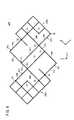
第1の実施の形態に係る積層導電シート(以下、第1積層導電シート10Aと記す)は、図1及び図2Aに示すように、第1導電シート12Aと第2導電シート12Bとが積層されて構成されている。x方向は、例えば後述する投影型静電容量方式のタッチパネル100(図7参照)の水平方向(又は垂直方向)あるいはタッチパネル100を設置した表示パネル110の水平方向(又は垂直方向)を示す。 As shown in FIGS. 1 and 2A, the laminated conductive sheet according to the first embodiment (hereinafter referred to as the first laminated
第1導電シート12Aは、図1及び図3に示すように、第1透明基体14A(図2A参照)の一主面上に形成された第1導電部16Aを有する。この第1導電部16Aは、それぞれ第1方向(x方向)に延在し、且つ、第1方向と直交する第2方向(y方向)に配列され、多数の格子にて構成された金属細線による2以上の第1導電パターン18Aと、各第1導電パターン18Aの周辺に配列された金属細線による第1補助パターン20Aとを有する。 As shown in FIGS. 1 and 3, the first
第1導電パターン18Aは、金属細線による2以上の第1大格子24A(第1感知部、第1パッド部)が第1方向に直列に接続されて構成され、各第1大格子24Aは、それぞれ2以上の小格子26が組み合わされて構成されている。また、第1大格子24Aの辺の周囲に、第1大格子24Aと非接続とされた上述の第1補助パターン20Aが形成されている。なお、小格子26は、ここでは一番小さい正方形状とされている。隣接する第1大格子24A間には、これら第1大格子24Aを電気的に接続する第1接続部28Aが形成されている。金属細線は例えば金(Au)、銀(Ag)又は銅(Cu)で構成されている。以下の説明では、金属細線を導線とも記す。 The first
図3に示すように、第1大格子24Aは、正方形の対角線上に位置する角部において小格子26の一部(本実施の形態では5つの小格子26)を除去した形状を有し、直線形状の4つの直辺30と、ジグザグ形状の2つの多角辺32とを有している。 As shown in FIG. 3, the first
1つの第1大格子24Aと第1接続部28Aとの接続点(接点)は、この例では3つ存在し、第1接点34、第2接点36及び第3接点38である。第1接点34は、第1大格子24Aに含まれる小格子26の頂点のうち、隣接する第1大格子24Aに最も近い頂点が対応する。第2接点36は、多角辺32に位置して第1接点34と隣接する頂点が対応する。第3接点38は、直辺30と多角辺32との交点であって隣接する第1大格子24Aに2番目に近い頂点が対応する。なお、後述する第2大格子24Bについても同様とする。また、隣接する第1大格子24Aのうち、両者を区別する場合には、一方の第1大格子24Aに参照符号24Aaを付し、他方の第1大格子24Aに参照符号24Abを付して説明する。 In this example, there are three connection points (contact points) between one first
第1接続部28Aは、1つの頂角を有し、一方の第1大格子24Aaの第1接点34と他方の第1大格子24Abの第2接点36との間を結ぶL字状の第1導線部40aと、1つの頂角を有し、他方の第1大格子24Abの第1接点34と一方の第1大格子24Aaの第2接点36との間を結ぶL字状の第2導線部40bとを有し、これら第1導線部40aと第2導線部40bとで1つの長方形部42を形づくっている。 The first connecting
ここで、第1方向と第2方向とを二等分する方向を第3方向(m方向)とし、第3方向と直交する方向を第4方向(n方向)としたとき、第1接続部28Aは、一方の第1大格子24Aaの第3接点38から第1導線部40aまで第4方向に延びる第3導線部40cと、他方の第1大格子24Abの第3接点38から第2導線部40bまで第4方向に延びる第4導線部40dとを有する。また、第1接続部28Aは、第1導線部40aと第3導線部40cとの交点P1、第2導線部40bと第3導線部40cとの交点P2、第2導線部40bと第4導線部40dとの交点P3、第1導線部40aと第4導線部40dとの交点P4を有する。すなわち、第1接続部28Aを構成する長方形部42は、一方の第1大格子24Aa側の第1長方形部42a(第1接点34、第2接点36、第1交点P1及び第2交点P2を有する)と、第1交点P1〜第4交点P4を有する第2長方形部42bと、他方の第1大格子24Ab側の第1長方形部42a(第1接点34、第2接点36、第3交点P3及び第4交点P4を有する)とを有する。 Here, when the direction bisecting the first direction and the second direction is the third direction (m direction), and the direction orthogonal to the third direction is the fourth direction (n direction), the
第1長方形部42aの長辺は小格子26の一辺の長さの3倍の長さを有し、短辺は小格子26の一辺の長さの2倍の長さを有する。また、第2長方形部42bの長辺は小格子26の一辺の長さの3倍の長さを有し、短辺は小格子26の一辺の長さを有する。すなわち、第1長方形部42aの互いに対向する金属細線(長辺)間の距離をLa、第2長方形部42bの互いに対向する金属細線(長辺)間の距離をLbとしたとき、La>Lbを満足する。好ましくは、1.2×Lb≦La≦3.0×Lbである。この例では、上述したように、距離Lbが小格子26の一辺の長さと同じであって、La=2×Lbである。 The long side of the first
図4に示すように、第1導線部40aは、一方の第1大格子24Aaの第1接点34から第4方向に延びた第1導線44aと、第1導線44aの先端から第1交点P1にかけて第3方向に延びる第2導線44bと、第1交点P1と第4交点P4とを結ぶ第3導線44cと、第4交点P4と他方の第1大格子24Abの第2接点36とを結ぶ第4導線44dとを有する。
第2導線部40bは、他方の第1大格子24Abの第1接点34から第4方向に延びた第5導線44eと、第5導線44eの先端から第3交点P3にかけて第3方向に延びる第6導線44fと、第3交点P3と第2交点P2とを結ぶ第7導線44gと、第2交点P2と一方の第1大格子24Aaの第2接点36とを結ぶ第8導線44hとを有する。
第3導線部40cは、一方の第1大格子24Aaの第3接点38と第2交点P2とを結ぶ第9導線44iと、第2交点P2と第1交点P1とを結ぶ第10導線44jとを有する。
第4導線部40dは、他方の第1大格子24Abの第3接点38と第4交点P4とを結ぶ第11導線44kと、第4交点P4と第3交点P3とを結ぶ第12導線44lとを有する。As shown in FIG. 4, the
The
The
The
上述のように構成された第1接続部28Aは、第1大格子24A間を3つ以上の接続経路で電気的に接続されることとなる。具体的には、第1接続部28Aは、第1大格子24Aaの第1接点34を通る場合に次の6つの接続経路を有する。
(1) 第1大格子24Aaの第1接点34から導線44a、44b、44c、44l、44f、44eを介して第1大格子24Abの第1接点34に繋がる第1接続経路(小格子の一辺の12倍の長さ)。
(2) 第1大格子24Aaの第1接点34から導線44a、44b、44j、44g、44f、44eを介して第1大格子24Abの第1接点34に繋がる第2接続経路(小格子の一辺の12倍の長さ)。
(3) 第1大格子24Aaの第1接点34から導線44a、44b、44c、44dを介して第1大格子24Abの第2接点36に繋がる第3接続経路(小格子の一辺の7倍の長さ)。
(4) 第1大格子24Aaの第1接点34から導線44a、44b、44j、44g、44l、44dを介して第1大格子24Abの第2接点36に繋がる第4接続経路(小格子の一辺の13倍の長さ)。
(5) 第1大格子24Aaの第1接点34から導線44a、44b、44c、44kを介して第1大格子24Abの第3接点38に繋がる第5接続経路(小格子の一辺の7倍の長さ)。
(6) 第1大格子24Aaの第1接点34から導線44a、44b、44j、44g、44l、44kを介して第1大格子24Abの第3接点38に繋がる第6接続経路(小格子の一辺の13倍の長さ)。The
(1) A first connection path (one side of the small lattice) connected from the
(2) A second connection path (one side of the small lattice) connected from the
(3) A third connection path (seven times as long as one side of the small lattice) that leads from the
(4) A fourth connection path (one side of the small lattice) connected from the
(5) A fifth connection path (seven times as large as one side of the small lattice) that leads from the
(6) A sixth connection path (one side of the small lattice) connected from the
なお、第1大格子24Aaの第2接点36を通る場合と、第1大格子24Aaの第3接点38を通る場合の具体的な接続経路の説明は省略するが、それぞれ6つの接続経路を有することとなるので、結果として、第1接続部28Aは、18通りの接続経路を有する。
つまり、一般化して述べると、一方の大格子と接続部との複数の接点から接続部内への金属細線の数をNa、接続部内の複数の交点間の金属細線の数をNb、他方の大格子と接続部との接点から接続部内への金属細線の数をNc、隣接する大格子間の接続経路の数をNとしたとき、
N=Na×(Nb+Nc−1)
である。The description of specific connection paths when passing through the
That is, in general terms, the number of fine metal wires from a plurality of contacts between one large lattice and the connection portion into the connection portion is Na, the number of fine metal wires between the plurality of intersections in the connection portion is Nb, and the other large When the number of fine metal wires from the contact point between the lattice and the connection portion into the connection portion is Nc, and the number of connection paths between adjacent large lattices is N,
N = Na × (Nb + Nc−1)
It is.
図3に示す第1接続部28Aの例では、図5Aに示すように、Na=3、Nb=4、Nc=3であるから、N=3×(4+3−1)=18となる。
第1接続部28Aの変形例として、図5Bや図5Cの例が考えられる。図5Bの第1変形例では、Na=4、Nb=7、Nc=4であるから、N=4×(7+4−1)=40となる。また、図5Cの第2変形例では、Na=4、Nb=12、Nc=4であるから、N=4×(12+4−1)=60となる。In the example of the first connecting
As a modification of the
さらに、第1接続部28Aは、第1長方形部42aの長辺(小格子26の一辺の長さの3倍以上の長さを有する)のうち、各第1接点34から第2長方形部42bに向かって直交して延びる金属細線による張り出し部(第1突出線52A)を有する。つまり、この張り出し部は第1接続部28A内に張り出した形態となっている。第1突出線52Aの長さは、小格子26の一辺の長さ同等の長さを有している。
また、隣接する第1導電パターン18A間は電気的に絶縁された第1絶縁部54Aが配されている。Furthermore, the first connecting
In addition, a first insulating
第1補助パターン20Aは、第1大格子24Aの辺のうち、第3方向と直交する辺に沿って配列された複数の第1補助線56A(第3方向を軸線方向とする)と、第1大格子24Aの辺のうち、第4方向と直交する辺に沿って配列された複数の第1補助線56A(第4方向を軸線方向とする)と、第1絶縁部54Aにおいて、それぞれ2つの第1補助線56AがL字状に組み合わされた2つの第1L字状パターン58Aが互いに対向して配置されたパターンとを有する。
各第1補助線56Aの軸線方向の長さは小格子26の内周に沿った1つの辺の1/2の長さを有する。また、各第1補助線56Aは、第1大格子24Aから所定距離(この例では、小格子26の内周に沿った1つの辺の1/2の長さ)だけ離間した位置に形成されている。The first
The length in the axial direction of each first auxiliary line 56 </ b> A has a length that is ½ of one side along the inner circumference of the
上述のように構成された第1導電シート12Aは、図1に示すように、各第1導電パターン18Aの一方の端部側に存在する第1大格子24Aの開放端は、第1接続部28Aが存在しない形状となっている。各第1導電パターン18Aの他方の端部側に存在する第1大格子24Aの端部は、第1結線部60Aを介して金属細線による第1端子配線パターン62Aに電気的に接続されている。 As shown in FIG. 1, the first
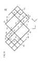
一方、第2導電シート12Bは、図1及び図6に示すように、第2透明基体14B(図2A参照)の一主面上に形成された第2導電部16Bを有する。この第2導電部16Bは、それぞれ第2方向(y方向)に延在し、且つ、第1方向(x方向)に配列され、多数の格子にて構成された金属細線による2以上の第2導電パターン18Bと、各第2導電パターン18Bの周辺に配列された金属細線による第2補助パターン20Bとを有する。 On the other hand, as shown in FIGS. 1 and 6, the second
第2導電パターン18Bは、金属細線による2以上の第2大格子24B(第2感知部、第2パッド部)が第2方向に直列に接続されて構成され、各第2大格子24Bは、それぞれ2以上の小格子26が組み合わされて構成されている。また、第2大格子24Bの辺の周囲に、第2大格子24Bと非接続とされた上述の第2補助パターン20Bが形成されている。隣接する第2大格子24B間には、これら第2大格子24Bを電気的に接続する第2接続部28Bが形成されている。 The second
図6に示すように、第2大格子24Bは、正方形の対角線上に位置する角部において小格子26の一部(本実施の形態では5つの小格子26)を除去した形状を有し、直線形状の4つの直辺30と、ジグザグ形状の2つの多角辺32とを有している。 As shown in FIG. 6, the second
以下の説明では、隣接する第2大格子24Bのうち、両者を区別する場合には、一方の第2大格子24Bに参照符号24Baを付し、他方の第2大格子24Bに参照符号24Bbを付して説明する。 In the following description, when distinguishing between the adjacent second
第2接続部28Bは、上述した第1接続部28Aと同様であるので、その重複説明を省略するが、1つの頂角を有し、一方の第2大格子24Baの第1接点34と他方の第2大格子24Bbの第2接点36との間を結ぶL字状の第5導線部40eと、1つの頂角を有し、他方の第2大格子24Bbの第1接点34と一方の第2大格子24Baの第2接点36との間を結ぶL字状の第6導線部40fとを有し、これら第5導線部40eと第6導線部40fとで1つの長方形部42を形づくっている。
第2接続部28Bは、一方の第2大格子24Baの第3接点38から第5導線部40eまで第4方向に延びる第7導線部40gと、他方の第2大格子24Bbの第3接点38から第6導線部40fまで第4方向に延びる第8導線部40hとを有する。
第5導線部40eは、第1導線部40aと同様に、図6において、参照符号の表記を省略するが、第1導線44a〜第4導線44dを有し、第6導線部40fは、第2導線部40bと同様に、第5導線44e〜第8導線44hを有し、第7導線部40gは、第3導線部40cと同様に、第9導線44i及び第10導線44jを有し、第8導線部40hは、第4導線部40dと同様に、第11導線44k及び第12導線44lを有する。
第2接続部28Bのその他の構成は、上述した第1接続部28Aと同様であるので、その重複説明を省略する。
この第2導電シート12Bにおいて、隣接する第2導電パターン18B間は電気的に絶縁された第2絶縁部54Bが配されている。Since the
The second connecting
Similarly to the
Since the other configuration of the
In the second
第2補助パターン20Bは、第2大格子24Bの辺のうち、第4方向と直交する辺に沿って配列された複数の第2補助線56B(第4方向を軸線方向とする)と、第2大格子24Bの辺のうち、第3方向と直交する辺に沿って配列された複数の第2補助線56B(第3方向を軸線方向とする)と、第2絶縁部54Bにおいて、それぞれ2つの第2補助線56BがL字状に組み合わされた2つの第2L字状パターン58Bが互いに対向して配置されたパターンとを有する。
各第2補助線56Bの軸線方向の長さは小格子26の内周に沿った1つの辺の1/2の長さを有する。また、各第2補助線56Bは、第2大格子24Bから所定距離(この例では、小格子26の内周に沿った1つの辺の1/2の長さ)だけ離間した位置に形成されている。The second
The length in the axial direction of each second auxiliary line 56 </ b> B has a length that is ½ of one side along the inner circumference of the
上述のように構成された第2導電シート12Bは、図1に示すように、1つ置き(例えば奇数番目)の第2導電パターン18Bの一方の端部側に存在する第2大格子24Bの開放端、並びに偶数番目の第2導電パターン18Bの他方の端部側に存在する第2大格子24Bの開放端には、それぞれ第2接続部28Bが存在しない形状となっている。一方、奇数番目の各第2導電パターン18Bの他方の端部側に存在する第2大格子24Bの端部、並びに偶数番目の各第2導電パターン18Bの一方の端部側に存在する第2大格子24Bの端部は、それぞれ第2結線部60Bを介して金属細線による第2端子配線パターン62Bに電気的に接続されている。 As shown in FIG. 1, the second
第1大格子24A及び第2大格子24Bの一辺の長さ(直辺30の長さ)は、3〜10mmであることが好ましく、4〜6mmであることがより好ましい。一辺の長さが、上記下限値未満であると、第1導電シート12A及び第2導電シート12Bを例えばタッチパネルに利用した場合に、検出時の第1大格子24A及び第2大格子24Bの静電容量が減るため、検出不良になる可能性が高くなる。他方、上記上限値を超えると、位置検出精度が低下する虞がある。同様の観点から、第1大格子24A及び第2大格子24Bを構成する小格子26の一辺の長さは50μm以上であることが好ましく、50〜500μmであることがより好ましく、150〜300μmであることがさらに好ましい。小格子26が上記範囲である場合には、さらに透明性も良好に保つことが可能であり、表示装置の前面にとりつけた際に、違和感なく表示を視認することができる。
また、第1導電パターン18A(第1大格子24A、第1接続部28A)の線幅、並びに第2導電パターン18B(第2大格子24B、第2接続部28B)の線幅は、それぞれ1〜15μmである。The length of one side (the length of the right side 30) of the first
Further, the line width of the first
第1補助パターン20A(第1補助線56A)及び第2補助パターン20B(第2補助線56B)の線幅はそれぞれ1〜15μmである。この場合、第1導電パターン18Aの線幅や第2導電パターン18Bの線幅と同じでもよく、異なっていてもよい。ただ、第1導電パターン18A、第2導電パターン18B、第1補助パターン20A及び第2補助パターン20Bの各線幅を同じにすることが好ましい。 The line widths of the first
ここで、上述の第1導電シート12A及び第2導電シート12Bを用いたタッチパネル100について図7も参照しながら説明する。
タッチパネル100は、センサ本体102と図示しない制御回路(IC回路等で構成)とを有する。センサ本体102は、図1、図2A及び図7に示すように、上述した第1導電シート12Aと第2導電シート12Bとが積層されて構成された第1積層導電シート10Aと、その上に積層された保護層106(図2Aでは保護層106の記述を省略している)とを有する。第1積層導電シート10A及び保護層106は、例えば液晶ディスプレイ等の表示装置108における表示パネル110上に配置されるようになっている。センサ本体102は、上面から見たときに、表示パネル110の表示画面110aに対応した領域に配されたセンサ部112と、表示パネル110の外周部分に対応する領域に配された端子配線部114(いわゆる額縁)とを有する。Here, the
The
タッチパネル100に適用した第1導電シート12Aは、図1に示すように、センサ部112に対応した部分に、上述した多数の第1導電パターン18Aが配列され、端子配線部114には各第1結線部60Aから導出された金属細線による複数の第1端子配線パターン62Aが配列されている。 As shown in FIG. 1, the first
図7の例では、第1導電シート12Aの外形は、上面から見て長方形状を有し、センサ部112の外形も長方形状を有する。端子配線部114のうち、第1導電シート12Aの一方の長辺側の周縁部には、その長さ方向中央部分に、複数の第1端子116aが前記一方の長辺の長さ方向に配列形成されている。また、センサ部112の一方の長辺(第1導電シート12Aの一方の長辺に最も近い長辺:y方向)に沿って複数の第1結線部60Aが直線状に配列されている。各第1結線部60Aから導出された第1端子配線パターン62Aは、第1導電シート12Aの一方の長辺におけるほぼ中央部に向かって引き回され、それぞれ対応する第1端子116aに電気的に接続されている。従って、センサ部112における一方の長辺の両側に対応する各第1結線部60Aに接続された第1端子配線パターン62Aは、ほぼ同じ長さにて引き回されることになる。もちろん、第1端子116aを第1導電シート12Aのコーナー部やその近傍に形成してもよいが、複数の第1端子配線パターン62Aのうち、最も長い第1端子配線パターン62Aと最も短い第1端子配線パターン62Aとの間に大きな長さ上の違いが生じ、最も長い第1端子配線パターン62Aとその近傍の複数の第1端子配線パターン62Aに対応する第1導電パターン18Aへの信号伝達が遅くなるという問題がある。そこで、本実施の形態のように、第1導電シート12Aの一方の長辺の長さ方向中央部分に、第1端子116aを形成することで、局所的な信号伝達の遅延を抑制することができる。これは、応答速度の高速化につながる。 In the example of FIG. 7, the outer shape of the first
同様に、第2導電シート12Bにおいても、センサ部112に対応した部分に、多数の第2導電パターン18Bが配列され、端子配線部114には各第2結線部60Bから導出された複数の第2端子配線パターン62Bが配列されている。
図7に示すように、端子配線部114のうち、第2導電シート12Bの一方の長辺側の周縁部には、その長さ方向中央部分に、複数の第2端子116bが前記一方の長辺の長さ方向に配列形成されている。また、センサ部112の一方の短辺(第2導電シート12Bの一方の短辺に最も近い短辺:x方向)に沿って複数の第2結線部60B(例えば奇数番目の第2結線部60B)が直線状に配列され、センサ部112の他方の短辺(第2導電シート12Bの他方の短辺に最も近い短辺:x方向)に沿って複数の第2結線部60B(例えば偶数番目の第2結線部60B)が直線状に配列されている。Similarly, in the second
As shown in FIG. 7, among the
複数の第2導電パターン18Bのうち、例えば奇数番目の第2導電パターン18Bが、それぞれ対応する奇数番目の第2結線部60Bに接続され、偶数番目の第2導電パターン18Bが、それぞれ対応する偶数番目の第2結線部60Bに接続されている。奇数番目の第2結線部60Bから導出された第2端子配線パターン62B並びに偶数番目の第2結線部60Bから導出された第2端子配線パターン62Bは、第2導電シート12Bの一方の長辺におけるほぼ中央部に向かって引き回され、それぞれ対応する第2端子116bに電気的に接続されている。従って、例えば第1番目と第2番目の第2端子配線パターン62Bは、ほぼ同じ長さにて引き回され、以下同様に、第2n−1番目と第2n番目の第2端子配線パターン62Bは、それぞれほぼ同じ長さにて引き回されることになる(n=1、2、3・・・)。 Among the plurality of second
もちろん、第2端子116bを第2導電シート12Bのコーナー部やその近傍に形成してもよいが、上述したように、最も長い第2端子配線パターン62Bとその近傍の複数の第2端子配線パターン62Bに対応する第2導電パターン18Bへの信号伝達が遅くなるという問題がある。そこで、本実施の形態のように、第2導電シート12Bの一方の長辺の長さ方向中央部分に、第2端子116bを形成することで、局所的な信号伝達の遅延を抑制することができる。これは、応答速度の高速化につながる。
なお、第1端子配線パターン62Aの導出形態を上述した第2端子配線パターン62Bと同様にし、第2端子配線パターン62Bの導出形態を上述した第1端子配線パターン62Aと同様にしてもよい。
そして、この第1積層導電シート10Aをタッチパネル100として使用する場合は、第1導電シート12A上に保護層を形成し、第1導電シート12Aの多数の第1導電パターン18Aから導出された第1端子配線パターン62Aと、第2導電シート12Bの多数の第2導電パターン18Bから導出された第2端子配線パターン62Bとを、例えばスキャンをコントロールする制御回路に接続する。Of course, the
The first
When this first laminated
タッチ位置の検出方式としては、自己容量方式や相互容量方式を好ましく採用することができる。すなわち、自己容量方式であれば、第1導電パターン18Aに対して順番にタッチ位置検出のための電圧信号を供給し、第2導電パターン18Bに対して順番にタッチ位置検出のための電圧信号を供給する。指先が保護層106の上面に接触又は近接させることで、タッチ位置に対向する第1導電パターン18A及び第2導電パターン18BとGND(グランド)間の容量が増加することから、当該第1導電パターン18A及び第2導電パターン18Bからの伝達信号の波形が他の導電パターンからの伝達信号の波形と異なった波形となる。従って、制御回路では、第1導電パターン18A及び第2導電パターン18Bから供給された伝達信号に基づいてタッチ位置を演算する。一方、相互容量方式の場合は、例えば第1導電パターン18Aに対して順番にタッチ位置検出のための電圧信号を供給し、第2導電パターン18Bに対して順番にセンシング(伝達信号の検出)を行う。指先が保護層106の上面に接触又は近接させることで、タッチ位置に対向する第1導電パターン18Aと第2導電パターン18B間の寄生容量に対して並列に指の浮遊容量が加わることから、当該第2導電パターン18Bからの伝達信号の波形が他の第2導電パターン18Bからの伝達信号の波形と異なった波形となる。従って、制御回路では、電圧信号を供給している第1導電パターン18Aの順番と、供給された第2導電パターン18Bからの伝達信号に基づいてタッチ位置を演算する。このような自己容量方式又は相互容量方式のタッチ位置の検出方法を採用することで、保護層106の上面に同時に2つの指先を接触又は近接させても、各タッチ位置を検出することが可能となる。なお、投影型静電容量方式の検出回路に関する先行技術文献として、米国特許第4,582,955号明細書、米国特許第4,686,332号明細書、米国特許第4,733,222号明細書、米国特許第5,374,787号明細書、米国特許第5,543,588号明細書、米国特許第7,030,860号明細書、米国公開特許第2004/0155871号明細書等がある。 As a touch position detection method, a self-capacitance method or a mutual capacitance method can be preferably employed. That is, in the case of the self-capacitance method, voltage signals for touch position detection are sequentially supplied to the first
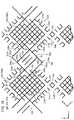
そして、例えば第2導電シート12B上に第1導電シート12Aを積層して第1積層導電シート10Aとしたとき、図8に示すように、第1導電パターン18Aと第2導電パターン18Bとが交差して配置された形態とされ、具体的には、第1導電パターン18Aの第1接続部28Aと第2導電パターン18Bの第2接続部28Bとが第1透明基体14A(図2A参照)を間に挟んで対向し、第1導電部16Aの第1絶縁部54Aと第2導電部16Bの第2絶縁部54Bとが第1透明基体14Aを間に挟んで対向した形態となる。なお、第1導電パターン18Aと第2導電パターン18Bの各線幅は同じであるが、図3、図6、図8〜図15、図17〜図24では、第1導電パターン18Aと第2導電パターン18Bの位置がわかるように、第1導電パターン18Aの線幅を太く、第2導電パターン18Bの線幅を細くして誇張して図示してある。 For example, when the first
積層した第1導電シート12A及び第2導電シート12Bを上面から見たとき、第1導電シート12Aに形成された第1大格子24Aの隙間を埋めるように、第2導電シート12Bの第2大格子24Bが配列された形態となる。つまり、大格子が敷き詰められた形態となる。このとき、第1大格子24Aと第2大格子24Bとの間に、第1補助パターン20Aと第2補助パターン20Bとが対向することによる組合せパターン75が形成される。 When the stacked first
組合せパターン75は、第1補助線56Aと第2補助線56Bとが直交して重ならない形態を有する。
すなわち、組合せパターン75のうち、第1大格子24Aの辺に沿って配列された第1補助線56Aと第2大格子24Bの辺に沿って配列された第2補助線56Bとによる組合せパターン75は、各第1補助線56Aの一方の端部(第1大格子24Aに遠い側の端部)が第2大格子24Bの直辺30に接続されたような形状になると共に、各第1補助線56Aの他方の端部(第1大格子24Aに近い側の端部)が第2補助線56Bの一方の端部(第2大格子24Bに近い側の端部)に接続されたような形状になり、同様に、各第2補助線56Bの他方の端部(第2大格子24Bに遠い側の端部)が第1大格子24Aの直辺30に接続されたような形状になって、結果的に複数の小格子26が配列された形態となり、第1大格子24Aと第2大格子24Bとの境界をほとんど見分けることができない状態となる。The
That is, in the
ここで、例えば第1補助パターン20A及び第2補助パターン20Bを形成しなかった場合は、組合せパターン75の幅に相当する空白領域が形成され、これにより、第1大格子24Aの境界、第2大格子24Bの境界が目立ってしまい、視認性が劣化するという問題が生じる。これを避けるために、第1大格子24Aの各直辺30に第2大格子24Bの直辺30を重ねて、空白領域をなくすことも考えられるが、重ね合わせの位置精度の僅かなズレにより、直線形状同士の重なり部分の幅が大きくなり(線太り)、これにより、第1大格子24Aと第2大格子24Bとの境界が目立ってしまい、視認性が劣化するという問題が生じる。
これに対して、本実施の形態では、上述したように、第1補助線56Aと第2補助線56Bとの重なりにより、第1大格子24Aと第2大格子24Bとの境界が目立たなくなり、視認性が向上する。Here, for example, when the first
On the other hand, in the present embodiment, as described above, the boundary between the first
また、上述したように、第1大格子24Aの各直辺30に第2大格子24Bの直辺30を重ねて、空白領域をなくした場合、第1大格子24Aの各直辺30の直下に第2大格子24Bの直辺30が位置することになる。このとき、第1大格子24Aの直辺30並びに第2大格子24Bの直辺30もそれぞれ導電部分として機能することから、第1大格子24Aの直辺30と第2大格子24Bの直辺30との間に寄生容量が形成され、この寄生容量の存在が電荷情報に対してノイズ成分として働き、S/N比の著しい低下を引き起こす。しかも、各第1大格子24Aと各第2大格子24B間に寄生容量が形成されることから、第1導電パターン18Aと第2導電パターン18Bに多数の寄生容量が並列に接続された形態となり、その結果、CR時定数が大きくなるという問題がある。CR時定数が大きくなると、第1導電パターン18A(及び第2導電パターン18B)に供給された電圧信号の波形の立ち上がり時間が遅くなり、所定のスキャン時間において位置検出のための電界の発生がほとんど行われなくなるおそれがある。また、第1導電パターン18A及び第2導電パターン18Bからの伝達信号の波形の立ち上がり時間又は立ち下がり時間も遅くなり、所定のスキャン時間において伝達信号の波形の変化を捉えることができなくなるおそれがある。これは、検出精度の低下、応答速度の低下につながる。つまり、検出精度の向上、応答速度の向上を図るためは、第1大格子24A及び第2大格子24Bの数を減らしたり(分解能の低減)、適応させる表示画面のサイズを小さくするしかなく、例えばB5版、A4版、それ以上の大画面に適用させることができないという問題が生ずる。 In addition, as described above, when the
これに対して、本実施の形態では、図2Aに示すように、第1大格子24Aの直辺30と、第2大格子24Bの直辺30との投影距離Lfを小格子26の一辺の長さとほぼ同じにしている。そのため、第1大格子24Aと第2大格子24B間に形成される寄生容量は小さくなる。その結果、CR時定数も小さくなり、検出精度の向上、応答速度の向上を図ることができる。なお、第1補助パターン20Aと第2補助パターン20Bとの組合せパターン75では、第1補助線56Aの端部と第2補助線56Bの端部とがそれぞれ対向する場合もあるが、第1補助線56Aは第1大格子24Aから非接続とされて電気的に絶縁となっており、第2補助線56Bも第2大格子24Bから非接続とされて電気的に絶縁となっているため、第1大格子24Aと第2大格子24B間に形成される寄生容量の増加にはつながらない。 On the other hand, in the present embodiment, as shown in FIG. 2A, the projection distance Lf between the
上述の投影距離Lfの最適距離は、第1大格子24A及び第2大格子24Bのサイズよりは、第1大格子24A及び第2大格子24Bを構成する小格子26のサイズ(線幅及び一辺の長さ)に応じて適宜設定することが好ましい。この場合、一定のサイズを有する第1大格子24A及び第2大格子24Bに対して、小格子26のサイズが大きすぎると、透光性は向上するが、伝達信号のダイナミックレンジが小さくなることから、検出感度の低下を引き起こすおそれがある。反対に、小格子26のサイズが小さすぎると、検出感度は向上するが、線幅の低減には限界があるため、透光性が劣化するおそれがある。 The optimum distance of the projection distance Lf described above is not the size of the first
そこで、上述の投影距離Lfの最適値(最適距離)は、小格子26の線幅を1〜15μmとしたとき、100〜400μmが好ましく、さらに好ましくは200〜300μmである。小格子26の線幅を狭くすれば、上述の最適距離も短くできるが、電気抵抗が高くなってくるため、寄生容量が小さくても、CR時定数が高くなってしまい、結果的に検出感度の低下、応答速度の低下を引き起こすおそれがある。従って、小格子26の線幅は上述の範囲が好ましい。 Therefore, the optimum value (optimum distance) of the projection distance Lf is preferably 100 to 400 μm, more preferably 200 to 300 μm, when the line width of the
そして、例えば表示パネル110のサイズあるいはセンサ部112のサイズとタッチ位置検出の分解能(駆動パルスのパルス周期等)とに基づいて、第1大格子24A及び第2大格子24Bのサイズ並びに小格子26のサイズが決定され、小格子26の線幅を基準に第1大格子24Aと第2大格子24B間の最適距離が割り出されることになる。
本実施の形態では、端子配線部114のうち、第1導電シート12Aの一方の長辺側の周縁部における長さ方向中央部分に複数の第1端子116aを形成し、第2導電シート12Bの一方の長辺側の周縁部における長さ方向中央部分に複数の第2端子116bを形成するようにしている。特に、図7の例では、第1端子116aと第2端子116bとが重ならないように、且つ、互いに接近した状態で配列し、さらに、第1端子配線パターン62Aと第2端子配線パターン62Bとが上下で重ならないようにしている。なお、第1端子116aと例えば奇数番目の第2端子配線パターン62Bとが一部上下で重なる形態にしてもよい。
これにより、複数の第1端子116a及び複数の第2端子116bを、2つのコネクタ(第1端子用コネクタ及び第2端子用コネクタ)あるいは1つのコネクタ(第1端子116a及び第2端子116bに接続される複合コネクタ)及びケーブルを介して制御回路に電気的に接続することができる。
また、第1端子配線パターン62Aと第2端子配線パターン62Bとが上下で重ならないようにしているため、第1端子配線パターン62Aと第2端子配線パターン62B間での寄生容量の発生が抑制され、応答速度の低下を抑えることができる。Then, for example, based on the size of the
In the present embodiment, a plurality of
Thereby, the plurality of
In addition, since the first
第1結線部60Aをセンサ部112の一方の長辺に沿って配列し、第2結線部60Bをセンサ部112の両側の短辺に沿って配列するようにしたので、端子配線部114の面積を縮小することができる。これは、タッチパネル100を含めた表示パネル110の小型化を促進させることができると共に、表示画面110aを印象的に大きく見せることができる。また、タッチパネル100としての操作性も向上させることができる。
端子配線部114の面積をさらに小さくするには、隣接する第1端子配線パターン62A間の距離、隣接する第2端子配線パターン62B間の距離を狭くすることが考えられるが、この場合、マイグレーションの発生防止を考慮すると、10μm以上50μm以下が好ましい。Since the
In order to further reduce the area of the
その他、上面から見たときに、隣接する第1端子配線パターン62A間に第2端子配線パターン62Bを配置することによって、端子配線部114の面積を小さくすることが考えられるが、パターンの形成ずれがあると、第1端子配線パターン62Aと第2端子配線パターン62Bとが上下で重なり、配線間の寄生容量が大きくなるおそれがある。これは応答速度の低下をもたらす。そこで、このような配置構成を採用する場合は、隣接する第1端子配線パターン62A間の距離を50μm以上100μm以下にすることが好ましい。
図7に示すように、第1導電シート12Aと第2導電シート12Bの例えば各コーナー部に、第1導電シート12Aと第2導電シート12Bの貼り合わせの際に使用する位置決め用の第1アライメントマーク118a及び第2アライメントマーク118bを形成することが好ましい。この第1アライメントマーク118a及び第2アライメントマーク118bは、第1導電シート12Aと第2導電シート12Bを貼り合わせて第1積層導電シート10Aとした場合に、新たな複合アライメントマークとなり、この複合アライメントマークは、該第1積層導電シート10Aを表示パネル110に設置する際に使用する位置決め用のアライメントマークとしても機能することになる。
この第1積層導電シート10Aにおいては、多数の第1導電パターン18A及び第2導電パターン18BのCR時定数を大幅に低減することができ、これにより、応答速度を速めることができ、駆動時間(スキャン時間)内での位置検出も容易になる。これは、タッチパネル100の画面サイズ(縦×横のサイズで、厚みを含まず)の大型化を促進できることにつながる。In addition, when viewed from above, it is conceivable to reduce the area of the
As shown in FIG. 7, the first alignment for positioning used when the first
In this first laminated
そして、第1接続部28Aと第2接続部28Bとが対向した部分を上面から見たとき、第1導電シート12Aにおける第1導線部40aの第1導線44aと第2導線44bとの交点が第2大格子24Bの多角辺32に位置する小格子26の頂点76に位置し、第2導電シート12Bにおける第5導線部40eの第1導線44aと第2導線44bとの交点が第1大格子24Aの多角辺32に位置する小格子26の頂点78に位置し、第1突出線52Aの各端部が第2接続部28Bの第1交点P1及び第3交点P3に位置し、第2突出線52Bの各端部が第1接続部28Aの第1交点P1及び第3交点P3に位置することとなり、これら第1接続部28Aにおける第1導線部40a〜第4導線部40d及び第1突出線52A並びに第2接続部28Bにおける第5導線部40e〜第8導線部40h及び第2突出線52Bの組み合わせによって、複数の小格子26が形成された形態となる。すなわち、第1接続部28Aと第2接続部28Bとが対向した部分に、第1接続部28Aと第2接続部28Bの組み合わせによって、複数の小格子26が配列された形態となり、周りの第1大格子24Aを構成する小格子26や第2大格子24Bを構成する小格子26と見分けがつかなくなり、視認性が向上する。 And when the part where 28 A of 1st connection parts and the
また、第1絶縁部54Aと第2絶縁部54Bとが対向した部分を上面から見たとき、第1L字状パターン58Aの屈曲部が第2大格子24Bの直辺30同士の交点に位置すると共に、第2L字状パターン58Bの屈曲部が第1大格子24Aの直辺30同士の交点に位置することとなり、これら第1L字状パターン58A及び第2L字状パターン58Bの組み合わせによって、複数の小格子26が配列された形態となる。その結果、周りの第1大格子24Aを構成する小格子26や第2大格子24Bを構成する小格子26と見分けがつかなくなり、視認性が向上する。 Further, when the portion where the first insulating
さらに、本実施の形態においては、第1接続部28Aによって第1大格子24A間を18通りの接続経路で接続しているので、例えば、第1接続部28Aにおいて、第2導線部40bの任意の部位と第3導線部40cの任意の部位とが断線したとしても、断線していない上述した第1接続経路等によって第1大格子24A間の電気的な接続が確保される。これにより、第1接続部28Aが完全に断線する蓋然性を従来よりも低くすることができる。 Furthermore, in the present embodiment, since the first
また、本実施の形態では、第1接続部28Aは、小格子26の一辺の長さの7倍の長さを有する接続経路(例えば、第3及び第5接続経路)と、小格子26の一辺の長さの8倍の長さを有する接続経路と、小格子26の一辺の長さの12倍の長さを有する接続経路(例えば、第1及び第2接続経路)と、小格子26の一辺の長さの13倍の長さを有する接続経路(例えば、第4及び第6接続経路)とを有し、各接続経路に含まれる第3導線44c及び第7導線44gの長さが小格子26の一辺の長さと同等の長さを有している。そのため、接続経路のうち第3導線44c及び第7導線44gが断線する確率は、1/7よりも低くなる。そのため、第1接続部28Aに含まれる2本の導線(第3導線44c及び第7導線44g)の両方が断線して第1接続部28Aが完全に断線する確率は相当低くなる。なお、小格子26の一辺の長さの8倍の長さを有する接続経路の例としては、第1大格子24Aaの第3接点38から第3導線部40c、第3導線44c及び第4導線44dを介して第1大格子24Abの第2接点36に繋がる接続経路等が挙げられる。 In the present embodiment, the
これは、第2接続部28Bにおいても同様であり、第2接続部28Bによって第2大格子24B間を18通りの接続経路で接続しているので、例えば、第2接続部28Bにおいて、第6導線部40fの任意の部位と第7導線部40gの任意の部位とが断線したとしても、断線していない上述した第1接続経路等によって第2大格子24B間の電気的な接続が確保される。これにより、第2接続部28Bが完全に断線する蓋然性を従来よりも低くすることができる。 The same applies to the
このように、第1積層導電シート10Aにおいては、該第1積層導電シート10Aを用いて例えば投影型静電容量方式のタッチパネルに適用した場合に、その表面抵抗が小さいことから応答速度を速めることができ、タッチパネルの大サイズ化を促進させることができる。また、電荷を蓄積するセルとして機能する第1大格子24A及び第2大格子24Bがそれぞれ多数の小格子26にて構成されていることから、第1大格子24A及び第2大格子24Bに蓄積される信号電荷の量が多くなり、その結果、入力に対する出力ダイナミックレンジが大きくなる。これにより、第1導電シート12A、あるいは第2導電シート12Bあるいは第1積層導電シート10Aをタッチパネルに使用した場合に、指先のタッチ位置を検出する感度(検出感度)を高めることができ、また、ノイズ成分に対する信号成分が大きくなることから、検出信号のS/N比を向上させることができる。これは、タッチ位置の検出精度の向上につながる。 As described above, in the first laminated
しかも、第1導電シート12Aの第1大格子24Aの周辺に形成された第1補助パターン20Aと第2導電シート12Bの第2大格子24Bの周辺に形成された第2補助パターン20Bとの組み合わせによって複数の小格子26が形づくられ、また、第1接続部28Aと第2接続部28Bとの組み合わせによって複数の小格子26が形づくられ、さらに、第1絶縁部54Aと第2絶縁部54Bとの組み合わせによって複数の小格子26が形づくられることから、第1導電シート12Aの第1大格子24Aと第2導電シート12Bの第2大格子24Bとの境界が目立たなくなり、局部的に線太りが生じる等の不都合もなくなり、全体として、視認性が良好となる。 In addition, a combination of the first
上述の第1積層導電シート10Aでは、小格子26の形状を正方形状としたが、その他、多角形状としてもよい。また、一辺の形状を直線状のほか、湾曲形状でもよいし、円弧状にしてもよい。円弧状とする場合は、例えば対向する2辺については、外方に凸の円弧状とし、他の対向する2辺については、内方に凸の円弧状としてもよい。また、各辺の形状を、外方に凸の円弧と内方に凸の円弧が連続した波線形状としてもよい。もちろん、各辺の形状を、サイン曲線にしてもよい。 In the first laminated
上述した第1導電シート12A及び第2導電シート12Bにおいては、第1導線44a及び第5導線44eの長さを小格子26の一辺の長さの2倍の長さに設定したが、その他、1.5倍、2.5倍、3倍等、種々の組み合わせに設定することができる。また、第1導線部40aの第3方向に沿った導線(第2導線44b、第3導線44c及び第4導線44d)、第2導線部40bの第3方向に沿った導線(第5導線44e、第6導線44f及び第7導線44g)、第3導線部40c、第4導線部40dのそれぞれの長さを小格子26の一辺の長さの5倍の長さに設定したが、その他、3倍、4倍、6倍等、種々の組み合わせに設定することができる。但し、第1接続部28A及び第2接続部28Bがあまりに大きすぎると、第1大格子24Aや第2大格子24Bの配置が難しくなり、また、交差部での静電容量変化が大きくなってノイズ成分が大きくなるため、第1導線44a及び第5導線44eの長さを小格子26の一辺の長さの4倍以下の長さに設定すると共に、第1導線部40aの第3方向に沿った導線、第2導線部40bの第3方向に沿った導線、第3導線部40c及び第4導線部40dのそれぞれの長さを小格子26の内周に沿った1つの辺の6倍以下の長さに設定することが好ましい。 In the first
また、第1接続部28Aは、3つ以上の接続経路を有する限り、その構成を任意に変更することができる。例えば、第1接続部28Aにおいて、第3導線部40c又は第4導線部40dを省略してもよい。この場合、第1接続部28Aは9通りの接続経路を有することとなる。つまり、第1接続部28Aは、第1大格子24Aaに含まれる1以上の小格子26の頂点と第1大格子24Abに含まれる1以上の小格子26の頂点との間を結ぶ3つ以上の導線を有していればよい。これは、第2接続部28Bにおいても同様である。 Moreover, as long as the
また、小格子26のサイズ(1辺の長さや対角線の長さ等)や、第1大格子24Aを構成する小格子26の個数、第2大格子24Bを構成する小格子26の個数も、適用されるタッチパネルのサイズや分解能(配線数)に応じて適宜設定することができる。 The size of the small lattice 26 (the length of one side, the length of the diagonal line, etc.), the number of
上述の第1積層導電シート10Aでは、図1及び図2Aに示すように、第1透明基体14Aの一主面に第1導電部16Aを形成し、第2透明基体14Bの一主面に第2導電部16Bを形成して、積層するようにしたが、その他、図2Bに示すように、第1透明基体14Aの一主面に第1導電部16Aを形成し、第1透明基体14Aの他主面に第2導電部16Bを形成するようにしてもよい。この場合、第2透明基体14Bが存在せず、第2導電部16B上に、第1透明基体14Aが積層され、第1透明基体14A上に第1導電部16Aが積層された形態となる。また、第1導電シート12Aと第2導電シート12Bとはその間に他の層が存在してもよく、第1導電部16Aと第2導電部16Bとが絶縁状態であれば、それらが対向して配置されてもよい。 In the first laminated
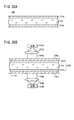
次に、第2の実施の形態に係る積層導電シート(以下、第2積層導電シート10Bと記す)について、図9〜図11を参照しながら説明する。
この第2積層導電シート10Bは、上述した第1積層導電シート10Aとほぼ同様の構成を有するが、図9に示すように、第1導電シート12Aの第1接続部28Aに張り出し部(第1突出線52A)が存在せず、図10に示すように、第2導電シート12Bの第2接続部28Bに張り出し部(第2突出線52B)が存在しない点で異なる。Next, a laminated conductive sheet according to the second embodiment (hereinafter referred to as a second laminated conductive sheet 10B) will be described with reference to FIGS.
The second laminated conductive sheet 10B has substantially the same configuration as the first laminated
従って、第1導電シート12Aと第2導電シート12Bを積層して第2積層導電シート10Bとした場合、図11に示すように、第1接続部28Aの第1交点P1に隣接する部分及び第3交点P3に隣接する部分にそれぞれ2つの小格子26を配列させた分の第1空白領域27Aが形成され、第2接続部28Bの第1交点P1に隣接する部分及び第3交点P3に隣接する部分にそれぞれ2つの小格子26を配列させた分の第2空白領域27Bが形成される。
この場合、規則的に第1空白領域27A及び第2空白領域27Bが配置され、しかも、各空白領域の大きさは、2つの小格子26が並んだ分の僅かな大きさであるため、ほとんど目立つことはないはないが、上述した第1積層導電シート10Aよりは視認性が劣ることになる。なお、第1積層導電シート10Aでは、第1接続部28Aに形成された張り出し部(第1突出線52A)によって第2空白領域27Bをそれぞれ2つに分断し、第2接続部28Bに形成された張り出し部(第2突出線52B)によって第1空白領域27Aをそれぞれ2つに分断するかたちになるため、図8にも示すように、周りの第1大格子24Aを構成する小格子26や第2大格子24Bを構成する小格子26と見分けがつかなくなり、視認性が向上する。Therefore, when the first
In this case, the first
次に、第3の実施の形態に係る積層導電シート(以下、第3積層導電シート10Cと記す)について、図12〜図14を参照しながら説明する。
この第3積層導電シート10Cは、上述した第1積層導電シート10Aとほぼ同様の構成を有するが、張り出し部が接続部から外に向かって張り出している点で異なる。
すなわち、第1接続部28Aは、図12に示すように、第1導線部40aの第3方向に沿った導線の第1交点P1と、第2導線部40bの第3方向に沿った導線の第3交点P3とからそれぞれ直交して延びる金属細線による張り出し部(第1突出線52A)を有する。
同様に、第2接続部28Bは、図13に示すように、第5導線部40eの第4方向に沿った導線の第1交点P1と、第6導線部40fの第4方向に沿った導線の第3交点P3とからそれぞれ直交して延びる金属細線による張り出し部(第2突出線52B)を有する。Next, a laminated conductive sheet according to a third embodiment (hereinafter referred to as a third laminated conductive sheet 10C) will be described with reference to FIGS.
The third laminated conductive sheet 10C has substantially the same configuration as the above-described first laminated
That is, as shown in FIG. 12, the first connection portion 28 </ b> A includes a first intersection P <b> 1 of the conductor along the third direction of the
Similarly, as shown in FIG. 13, the second connecting
従って、第1導電シート12Aと第2導電シート12Bを積層して第3積層導電シート10Cとした場合、図14に示すように、第1接続部28Aに形成された張り出し部(第1突出線52A)によって第1空白領域27A(図11参照)をそれぞれ2つに分断し、第2接続部28Bに形成された張り出し部(第2突出線52B)によって第2空白領域27B(図11参照)をそれぞれ2つに分断するかたちになるため、周りの第1大格子24Aを構成する小格子26や第2大格子24Bを構成する小格子26と見分けがつかなくなり、視認性が向上する。 Therefore, when the first
次に、第4の実施の形態に係る積層導電シート(以下、第4積層導電シート10Dと記す)について、図15〜図18を参照しながら説明する。
この第4積層導電シート10Dは、上述した第1積層導電シート10Aとほぼ同様の構成を有するが、以下の点で異なる。
すなわち、図15及び図16に示すように、第1接続部28Aの第3導線部40cは、1つの頂角を有し、一方の第1大格子24Aaの第3接点38と他方の第1大格子24Abの第3接点38との間を結ぶL字状の導線部として形成され、第4導線部40dは、1つの頂角を有し、他方の第1大格子24Abの第3接点38と一方の第1大格子24Aaの第3接点38との間を結ぶL字状の導線部として形成されている。さらに、第1大格子24Aの第3方向(m方向)に沿った辺と第1導線部40a及び第2導線部40bとの間にそれぞれ小格子26の一辺の長さ分だけ欠除された部分(第1欠除部80A)が形成されると共に、1つ分の第1補助線56Aも欠除された形態となっている。第1接点34は存在しない。
同様に、図17に示すように、第2接続部28Bの第7導線部40gは、1つの頂角を有し、一方の第2大格子24Baの第3接点38と他方の第2大格子24Bbの第3接点38との間を結ぶL字状の導線部として形成され、第8導線部40hは、1つの頂角を有し、他方の第2大格子24Bbの第3接点38と一方の第2大格子24Baの第3接点38との間を結ぶL字状の導線部として形成されている。また、第2大格子24Bの第4方向(n方向)に沿った辺と第5導線部40e及び第6導線部40fとの間にそれぞれ小格子26の一辺の長さ分だけ欠除された部分(第2欠除部80B)が形成されると共に、1つ分の第2補助線56Bも欠除された形態となっている。この場合も第1接点34は存在しない。
なお、図17において参照符号の表記を省略するが、第7導線部40gは、第1接続部28Aにおける第3導線部40cと同様に、第9導線44i、第10導線44j、第13導線44m及び第14導線44nを有する。第8導線部40hは、第1接続部28Aにおける第4導線部40dと同様に、第11導線44k、第12導線44l、第15導線44o及び第16導線44pを有する。Next, a laminated conductive sheet (hereinafter referred to as a fourth laminated conductive sheet 10D) according to a fourth embodiment will be described with reference to FIGS.
The fourth laminated conductive sheet 10D has substantially the same configuration as the first laminated
That is, as shown in FIGS. 15 and 16, the
Similarly, as shown in FIG. 17, the seventh conductor portion 40g of the
Although notation of reference numerals is omitted in FIG. 17, the seventh conductor portion 40g is similar to the
従って、この第4積層導電シート10Dの第1接続部28Aにおいては、一方の第1大格子24Aaと第1接続部28Aとの複数の接点から第1接続部28A内への金属細線の数Naが4、第1接続部28A内の複数の交点間の金属細線の数Nbが4、他方の第1大格子24Abと第1接続部28Aとの複数の接点から第1接続部28A内への金属細線の数Ncが4となるため、隣接する第1大格子24A間の接続経路の数Nは、N=4×(4+4−1)=28となり、第1積層導電シート10Aの第1導電シート12Aにおける第1接続部28Aの接続経路の数(=18)よりも10だけ多くなっている。そのため、第1接続部28Aが完全に断線する蓋然性をさらに低くすることができ、信頼性の向上を高めることができる。これは、第2接続部28Bにおいても同様である。 Accordingly, in the
また、この第4積層導電シート10Dにおいては、第1接続部28Aの第3導線部40cを構成する第13導線44mと、第4導線部40dを構成する第15導線44oが第3積層導電シート10Cにおける第1接続部28Aの張り出し部(第1突出線52A)と同様の機能を果たし、同様に、第2接続部28Bの第7導線部40gを構成する第13導線44mと、第8導線部40hを構成する第15導線44oが第3積層導電シート10Cにおける第2接続部28Bの張り出し部(第2突出線52B)と同様の機能を果たすことになる。 Further, in the fourth laminated conductive sheet 10D, the thirteenth
すなわち、第1導電シート12Aと第2導電シート12Bを積層して第4積層導電シート10Dとした場合、図18に示すように、第1接続部28Aに形成された第3導線部40cの第13導線44m及び第14導線44nと第4導線部40dの第15導線44o及び第16導線44pとによって第1空白領域27A(図11参照)をそれぞれ2つに分断すると共に、第2欠除部80B及び欠除された1つ分の第2補助線56Bに相当する空白を補完するかたちになり、また、第2接続部28Bに形成された第7導線部40gの第13導線44m及び第14導線44nと第8導線部40hの第15導線44o及び第16導線44pとによって第2空白領域27B(図11参照)をそれぞれ2つに分断すると共に、第1欠除部80A及び欠除された1つ分の第1補助線56Aに相当する空白を補完するかたちになるため、周りの第1大格子24Aを構成する小格子26や第2大格子24Bを構成する小格子26と見分けがつかなくなり、視認性が向上する。 That is, when the first
次に、第5の実施の形態に係る積層導電シート(以下、第5積層導電シート10Eと記す)について、図19〜図21を参照しながら説明する。
この第5積層導電シート10Eは、上述した第1積層導電シート10Aと比較して以下の点で異なる。
すなわち、図19に示すように、本実施の形態に係る第1導電部16Aでは、第1導電パターン18Aを構成する第1大格子24Aの間隔が広くなると共に、第1絶縁部54Aの領域が広くなっている。
つまり、第1接続部200Aは、1つの頂角を有し、一方の第1大格子24Aaの第1接点34と他方の第1大格子24Abの第2接点36とを結ぶL字状の第1導線部202aと、1つの頂角を有し、他方の第1大格子24Abの第1接点34と一方の第1大格子24Aaの第2接点36との間を結ぶL字状の第2導線部202bとを有し、これら第1導線部202aと第2導線部202bとを含んで1つの長方形部204を形づくっている。なお、長方形部204は、上述した長方形部42よりも一回り大きくなっている。
また、第1接続部200Aは、一方の第1大格子24Aaの第3接点38から第1導線部202aまで第4方向に延びる第3導線部202cと、他方の第1大格子24Abの第3接点38から第2導線部202bまで第4方向に延びる第4導線部202dとを有する。Next, a laminated conductive sheet according to a fifth embodiment (hereinafter referred to as a fifth laminated
The fifth laminated
That is, as shown in FIG. 19, in the first
In other words, the first connecting
The
第1接続部200Aは、第1導線部202aと第3導線部202cとの交点P1、第2導線部202bと第3導線部202cとの交点P2、第2導線部202bと第4導線部202dとの交点P3、第1導線部202aと第4導線部202dとの交点P4を有する。
長方形部204は、長方形部42と同様に、第1長方形部204a及び第2長方形部204bを有する。第1長方形部204aの長辺は小格子26の一辺の長さの5倍の長さを有し、短辺は小格子26の一辺の長さの2倍の長さを有する。第2長方形部204bの長辺は小格子26の一辺の長さの5倍の長さを有し、短辺は小格子26の一辺の長さの3倍の長さを有する。200 A of 1st connection parts are the intersection P1 of the
Similar to the
また、第1接続部200Aは、4つの張り出し部(突出線208A)を有する。具体的には、突出線208Aは、第1導線部202aの第4方向に沿った導線のうち一方の第1大格子24Aaの第1接点34から小格子26の一辺の長さ分だけ離間した位置と、第1導線部202aの第3方向に沿った導線のうち第4交点P4から第1交点P1側に小格子26の一辺の長さ分だけ離間した位置と、第2導線部202bの第4方向に沿った導線のうち他方の第1大格子24Abの第1接点34から小格子26の一辺の長さ分だけ離間した位置と、第2導線部202bの第3方向に沿った導線のうち第2交点P2から第3交点P3側に小格子26の一辺の長さ分だけ離間した位置とに接続されている。なお、突出線208Aは、小格子26の一辺の長さと同等の長さを有した直線状の金属細線を2本接続してL字状に形成されている。
なお、図19から諒解されるように、第1大格子24Aの第1接点34には突出線52Aが設けられている。Further, the
As can be seen from FIG. 19, the
第1補助パターン212Aは、第1接続部200Aを構成する第2長方形部204b内に配置された平行な一対の補助線210と、第1大格子24Aの辺のうち、第3方向と直交する辺に沿って配列されたコ字状パターン(門型形状パターン)218Aと、第1大格子24Aの辺のうち、第4方向と直交する辺に沿って配列されたコ字状パターン(門型形状パターン)218Aと、第1絶縁部54Aに位置する四角環状パターン220とを有する。
一対の補助線210は、第4方向の位置を揃えた状態で第3方向に離間している。各コ字状パターン218Aは、小格子26の一辺と同一の長さを有した3つの直線状の金属細線によって構成されている。各コ字状パターン218Aは、第1大格子24Aから所定距離(この例では、小格子26の一辺の長さ)だけ離間した位置に形成されている。四角環状パターン220は、小格子26と同一の形状及び大きさに構成されている。また、図19から諒解されるように、第4方向において、四角環状パターン220とコ字状パターン218Aとの間には、第3方向に延びた補助線214が設けられている。The first
The pair of auxiliary lines 210 are separated in the third direction with their positions in the fourth direction aligned. Each U-shaped pattern 218 </ b> A is configured by three straight metal thin wires having the same length as one side of the
また、図20に示すように、本実施の形態に係る第2導電部16Bでは、第2大格子24Bが一回り大きく形成されている。つまり、第2大格子24Bは、第1大格子24Aよりも一回り大きい略正方形状に形成されている。
1つの第2大格子24Bと第2接続部200Bとの接続点(接点)は、この例では4つ存在し、第1接点222、第2接点224、第3接点226及び第4接点228である。第1接点222は、第4方向に延びた直辺30と多角辺32との交点が対応する。第2接点224は、第2大格子24Bに含まれる小格子26の頂点のうち、多角辺32に位置して第1接点222から小格子26の一辺の長さの2倍の距離だけ離れた頂点が対応する。第3接点226は、第3方向に沿って延びた直辺30と多角辺32との交点が対応する。第4接点228は、第2大格子24Bに含まれる小格子26の頂点のうち、多角辺32に位置して第3接点226に隣接する頂点が対応する。
第2大格子24Bには、小格子26の頂点のうち、多角辺32における第1接点222及び第2接点224の間に位置する頂点から第4方向に延びた突出線230が設けられている。Further, as shown in FIG. 20, in the second
In this example, there are four connection points (contact points) between one second
The second large lattice 24 </ b> B is provided with a
第2接続部200Bは、2つの頂角を有し、一方の第2大格子24Baの第1接点222と他方の第2大格子24Bbの第2接点224との間を結ぶ第5導線部202eと、2つの頂角を有し、他方の第2大格子24Bbの第1接点222と一方の第2大格子24Baの第2接点224との間を結ぶ第6導線部202fと、一方の第2大格子24Baの第3接点226から第5導線部202eまで第3方向に延びる第7導線部202gと、他方の第2大格子24Bbの第3接点226から第6導線部202fまで第3方向に延びる第8導線部202hと、一方の第2大格子24Baの第4接点228から第5導線部202eまで第3方向に延びる第9導線部202iと、他方の第2大格子24Bbの第4接点228から第6導線部202fまで第3方向に延びる第10導線部202jとを有する。
また、第2接続部200Bは、第5導線部202eと第7導線部202gとの交点P1と、第5導線部202eと第8導線部202hとの交点P2と、第5導線部202eと第10導線部202jとの交点P3と、第6導線部202fと第9導線部202iとの交点P4と、第6導線部202fと第7導線部202gとの交点P5と、第6導線部202fと第8導線部202hとの交点P6とを有する。The second connecting portion 200B has two apex angles, and a
The second connecting portion 200B includes an intersection P1 between the
従って、この第5積層導電シート10Eの第2接続部200Bにおいて、一方の第2大格子24Baと第2接続部200Bとの複数の接点から第2接続部200B内への金属細線の数Naが4、第2接続部200B内の複数の交点間の金属細線の数Nbが8、他方の第2大格子24Bbと第2接続部200Bとの複数の接点から第2接続部28B内への金属細線の数Ncが4となるため、隣接する第2大格子24B間の接続経路の数Nは、N=4×(8+4−1)=44となり、第1積層導電シート10Aの第2導電部16Bにおける第2接続部28Bの接続経路の数(=18)よりも26だけ多くなっている。そのため、第2接続部200Bが完全に断線する蓋然性をさらに低くすることができ、信頼性の向上を高めることができる。 Therefore, in the second connection portion 200B of the fifth laminated
第2接続部200Bは、4つの直線状の張り出し部(突出線208B)と、3つの頂角を有する一対の張り出し部(突出線232)とを有する。突出線208Bは、第5導線部202eの第3方向に沿った導線のうち第9導線部202iとの交点から第1交点P1側に小格子26の一辺の長さ分だけ離間した位置と、第1交点P1と、第6導線部202fの第3方向に沿った導線のうち第10導線部202jとの交点から第6交点P6側に小格子26の一辺の長さ分だけ離間した位置と、第6交点P6とに接続されている。
突出線232は、第5導線部202eのうち他方の第2大格子24Bb側の頂角(角部)と、第6導線部202fのうち一方の第2大格子24Ba側の頂角(角部)とに接続されている。
図20から諒解されるように、突出線232は、第5導線部202e(又は第6導線部202f)から外側(第4方向)に延びた第1直線234と、第1直線234の先端から第2大格子24B側に延びた第2直線236と、第2直線236の先端から外側に延びた第3直線238と、第3直線238の先端から第2大格子24Bが位置する側とは反対側に延びた第4直線240とを含む。The second connecting portion 200B has four linear protruding portions (projecting
The protruding
As can be seen from FIG. 20, the protruding
第2補助パターン212Bは、第2大格子24Bの辺のうち、第3方向と直交する辺に沿って配列されたコ字状パターン(門型形状パターン)218Bと、第2大格子24Bの辺のうち、第4方向と直交する辺に沿って配列されたコ字状パターン(門型形状パターン)218Bと、隣接する第2導電パターン18Bを構成する第2大格子24Bと前記コ字状パターン218Bとの間に設けられた複合パターン242とを有する。
各コ字状パターン218Bは、小格子26の一辺と同一の長さを有した3つの直線状の金属細線によって構成されている。各コ字状パターン218Bは、第2大格子24Bから所定距離(この例では、小格子26の一辺の長さ)だけ離間した位置に形成されている。複合パターン242は、四角環状パターン及びL字状パターンを接続してアラビア数字の9又は6の形態に形成されている。四角環状パターンは、小格子26と同一の形状及び大きさに構成され、L字状パターンは、軸方向の長さが小格子26の一辺と同一の長さを有した2つの直線状の金属細線によって構成されている。The second
Each U-shaped pattern 218 </ b> B is composed of three straight metal thin wires having the same length as one side of the
従って、第1導電シート12Aと第2導電シート12Bを積層して第5積層導電シート10Eとした場合、第1導電部16Aに対して、突出線52A、突出線208A及び第1補助パターン212Aを設けると共に、第2導電部16Bに対して、突出線230、突出線208B、突出線232及び第2補助パターン212Bを設けているので、第1大格子24Aを構成する小格子26や第2大格子24Bを構成する小格子26と見分けがつかなくなり、視認性が向上する(図21参照)。 Accordingly, when the first
本実施の形態では、第2大格子24Bを第1大格子24Aよりも大きく形成しているが、第2大格子24Bを第1大格子24Aよりも小さく形成してもよい。このように、第1大格子24Aと第2大格子24Bの大きさを異ならせることができるので、第1導電シート12Aと第2導電シート12Bの組み合わせのバリエーションを増加させることができる。 In the present embodiment, the second
次に、第6の実施の形態に係る積層導電シート(以下、第6積層導電シート10Fと記す)について、図22〜図24を参照しながら説明する。
この第6積層導電シート10Fは、上述した第5積層導電シート10Eに対して以下の点で異なる。
すなわち、図22に示すように、本実施の形態に係る第1導電部16Aでは、第1接続部250Aの構成が異なる。第1接続部250Aは、第1導線部202aと同一形状の第1導線部252aと、第2導線部202bと同一形状の第2導線部252bとを有し、これら第1導線部252aと第2導線部252bとを含んで1つの長方形部254を形づくっている。
また、第1接続部250Aは、一方の第1大格子24Aaの第3接点38から第2導線部252bまで第4方向に延びる第3導線部252cと、他方の第1大格子24Abの第3接点38から第1導線部252aまで第4方向に延びる第4導線部252dと、第1導線部252aの第3方向に沿った導線と第2導線部252bの第3方向に沿った導線とを結ぶ第5導線部252e及び第6導線部252fとを有する。Next, a laminated conductive sheet according to a sixth embodiment (hereinafter referred to as a sixth laminated
The sixth laminated
That is, as shown in FIG. 22, the configuration of the first connecting
The first connecting
第1接続部250Aは、第1導線部252aと第5導線部252eとの交点P1、第2導線部252bと第5導線部252eとの交点P2、第2導線部252bと第6導線部252fとの交点P3、第1導線部252aと第6導線部252fとの交点P4を有する。
長方形部254は、長方形部204と同様に、第1長方形部254a及び第2長方形部254bを有する。第1長方形部254aの長辺は小格子26の一辺の長さの5倍の長さを有し、短辺は小格子26の一辺の長さの3倍の長さを有する。第2長方形部254bの長辺は小格子26の一辺の長さの5倍の長さを有し、短辺は小格子26の一辺の長さと同一の長さを有する。そのため、本実施の形態に係る第1接続部250Aでは、La>Lbを満足する。この例では、La=3×Lbである。250 A of 1st connection parts are the intersection P1 of the
The
また、第1接続部250Aには、4つの張り出し部(突出線256)が設けられている。具体的には、突出線256は、第5導線部252eのうち第1交点P1から小格子26の一辺の長さの2倍の長さ分だけ離間した位置と、第5導線部252eのうち第2交点P2から小格子26の一辺の長さの2倍の長さ分だけ離間した位置と、第6導線部252fのうち第3交点P3から小格子26の一辺の長さの2倍の長さ分だけ離間した位置と、第6導線部252fのうち第4交点P4から小格子26の一辺の長さの2倍の長さ分だけ離間した位置とに接続されている。突出線256は、小格子26の一辺の長さの2倍の長さを有した直線状の金属細線により構成されている。
なお、図22から諒解されるように、第1大格子24Aの第1接点34には突出線52Aが設けられている。The first connecting
As can be understood from FIG. 22, the
第1補助パターン258Aは、第1大格子24Aの辺のうち、第3方向と直交する辺に沿って配列された複数の補助長線260と、これら補助長線260の間に設けられた補助短線262と、第1大格子24Aの第3方向に沿って延びた直辺30に対向配置された複合パターン264とを有する。
各補助長線260の軸方向の長さは、小格子26の一辺の長さの2倍の長さを有する。各補助長線260は、第1大格子24Aから所定距離(この例では、小格子26の一辺の長さ)だけ離間した位置に形成されている。各補助短線262の軸方向の長さは、小格子26の一辺の長さと同一である。各補助短線262は、第1大格子24Aから所定距離(この例では、小格子26の一辺の長さの2倍の長さ)だけ離間した位置に形成されている。
なお、図22から諒解されるように、第1接続部250Aに最も近い補助長線260における第1大格子24A側の端部には、第4方向に沿って延びた補助線266が接続されている。つまり補助長線260及び補助線266が組み合わされてL字状パターンを構成している。
複合パターン264は、第1大格子24Aの辺のうち、第4方向と直交する辺に沿って配列された複数(図22では5つ)の補助線268と、これら補助線268の第1大格子24A側の端部を連結する長尺な補助線270と、補助線270の第1絶縁部54A側の端部に接続されて第4方向に沿って延びた補助線272と、補助線272から第3方向に沿って延びた一対の補助線274a、274bとを有する。
補助線268及び補助線274a、274bの軸方向の長さは、小格子26の一辺の長さと同一である。各補助線268は、第1大格子24Aから所定距離(この例では、小格子26の一辺の長さ)だけ離間した位置に形成されている。つまり、複合パターン264は、第1大格子24Aから離間している。
図22から諒解されるように、補助線274aは、補助線268の1つに接続して四角環状パターンを形成しており、補助線274bは、補助線272における第1大格子24Aが位置する側とは反対側の端部に接続している。The first
The length of each auxiliary
As can be seen from FIG. 22, an
The
The lengths of the
As can be seen from FIG. 22, the
また、図23に示すように、本実施の形態に係る第2導電部16Bでは、第2大格子24Bが略長方形状に形成されている。つまり、第2大格子24Bは、第1大格子24Aに対して大きさ及び形状が異なっている。なお、この例では、第2大格子24Bの長辺は第4方向に沿って延在している。
1つの第2大格子24Bと第2接続部250Bとの接続点(接点)は、第1接点222、第2接点300、第3接点226及び第4接点228である。第2接点300は、第2大格子24Bに含まれる小格子26の頂点のうち、多角辺32に位置して第1接点222から小格子26の一辺の長さだけ離間した頂点が対応する。なお、図20に示す突出線230は省略されている。As shown in FIG. 23, in the second
Connection points (contact points) between one second
第2接続部250Bは、第5導線202eと同一形状の第7導線部252gと、第6導線部202fと同一構成の第8導線部252hと、一方の第2大格子24Baの第3接点226から第8導線部252hまで第3方向に延びる第9導線部252iと、他方の第2大格子24Bbの第3接点226から第7導線部252gまで第3方向に延びる第10導線部252jと、1つの頂角を有し、第7導線部252gに接すると共に一方の第2大格子24Baの第4接点228と第8導線部252hとを結ぶ第11導線部252kと、1つの頂角を有し、第8導線部252hに接すると共に他方の第2大格子24Bbの第4接点228と第7導線部252gとを結ぶ第12導線部252lとを有する。
また、第2接続部250Bは、第7導線部252gの第3方向に沿った導線と第12導線部252lの第4方向に沿った導線との交点P1、第7導線部252gと第11導線部252kとの交点P2、第8導線部252hの第4方向に沿った導線と第11導線部252kの第3方向に沿った導線との交点P3、第7導線部252gの第4方向に沿った導線と第12導線部252lの第3方向に沿った導線との交点P4、第8導線部252hと第12導線部252lとの交点P5、第8導線部252hの第3方向に沿った導線と第11導線部252kの第4方向に沿った導線との交点P6を有する。The
In addition, the second connecting
これにより、第7導線部252gのうち第2交点P2及び第4交点P4間の導線、第8導線部252hのうち第3交点P3及び第5交点P5間の導線、第11導線部252kのうち第2交点P2及び第3交点P3間の導線、及び第12導線部252lのうち第4交点P4及び第5交点P5間の導線によって長方形部302が形成される。
長方形部302の長辺は第3方向に沿って延在している。長方形部302は、一方の第2大格子24Ba側の小さい長方形部302a(第2交点P2、第3交点P3及び第6交点P6を有する)と、第1交点P1、第2交点P2、第5交点P5及び第6交点P6を有する正方形部302bと、他方の第2大格子24Bb側の小さい長方形部302a(第1交点P1、第4交点P4及び第5交点P5を有する)とを含む。
長方形部302aの長辺は小格子26の一辺の長さの4倍の長さを有し、短辺は小格子26の一辺の長さと同一の長さを有する。正方形部302bの一辺は小格子26の一辺の長さの3倍の長さを有する。そのため、本実施の形態に係る第2接続部250Bは、La>Lbを満足する。この例では、La=3×Lbである。Accordingly, among the
The long side of the
The long side of the
また、第2接続部250Bは、一対の直線状の張り出し部(突出線304)と、1つの頂角を有する一対の張り出し部(突出線306)と、2つの頂角を有する一対の張り出し部(突出線308)とを有する。突出線304は、第1交点P1及び第6交点P6に接続されている。
一対の突出線306は、第7導線部252gのうち第4交点P4から小格子26の一辺の長さの2倍の長さ分だけ第1交点P1側に移動した位置と、第8導線部252hのうち第3交点P3から小格子26の一辺の長さの2倍の長さ分だけ第6交点P6側に移動した位置とに接続されている。各突出線306は、L字状に形成されている。
一対の突出線308は、第7導線部252gのうち他方の第2大格子24Bb側の頂角(角部)と、第8導線部252hのうち一方の第2大格子24Ba側の頂角(角部)とに接続されている。各突出線308は、第7導線部252g(又は第8導線部252h)から外側(第4方向)に延びた第1直線310と、第1直線310の先端から第2大格子24B側に延びた第2直線312と、第2直線312の先端から内側に延びた第3直線314とを含む。The second connecting
The pair of protruding
The pair of protruding
第2補助パターン258Bは、第2接続部250Bを構成する第2長方形部254b内に配置された平行な一対の補助線315と、第2大格子24Bの辺のうち、第4方向に直交する辺に沿って配列された複数の補助線316と、第2大格子24Bの第4方向に沿って延びた直辺30に対向配置された複合パターン318と、第2絶縁部54Bに配置された平行な一対の補助線320とを有する。
一対の補助線315は、第3方向の位置を揃えた状態で第4方向に離間している。なお、一対の補助線320も同様である。各補助線315、316、320の軸方向の長さは、小格子26の一辺の長さと同一の長さを有する。各補助線316は、第2大格子24Bから所定距離(この例では、小格子26の一辺の長さ)だけ離間した位置に形成されている。
複合パターン318は、第2大格子24Bの辺のうち、第3方向と直交する辺に沿って交互に配置された補助長線322及び補助短線324と、補助長線322の第2大格子24B側の端部を連結して第4方向に延びた長尺な補助線326と、補助短線324の第2大格子24B側の端部を連結して第4方向に延びた長尺な補助線328と、補助線328の第2絶縁部54B側の端部同士を連結して第3方向に延びた補助線330と、補助線330のうち第2大格子24Bが位置する側とは反対側の端部から外側に延びた補助線332とを有する。
各補助長線322の軸方向の長さは、小格子26の一辺の長さの2倍の長さである。各補助長線322は、第2大格子24Bから所定距離(この例では、小格子26の一辺の長さ)だけ離間した位置に形成されている。各補助短線324の軸方向の長さは、小格子26の一辺の長さと同一である。各補助短線324は、第2大格子24Bから所定距離(この例では、小格子26の一辺の長さの2倍の長さ)だけ離間した位置に形成されている。つまり、複合パターン318は、第2大格子24Bから離間している。The second
The pair of
The
The length of each auxiliary
従って、第1導電シート12Aと第2導電シート12Bを積層して第6積層導電シート10Fとした場合、第1導電部16Aに対して、突出線52A、突出線256及び第1補助パターン258Aを設けると共に、第2導電部16Bに対して、突出線304、突出線306、突出線312及び第2補助パターン258Bを設けているので、第1大格子24Aを構成する小格子26や第2大格子24Bを構成する小格子26と見分けがつかなくなり、視認性が向上する(図24参照)。 Accordingly, when the first
本実施の形態では、第1大格子24Aを略正方形状に形成すると共に第2大格子24Bを略長方形状に形成しているが、第1大格子24Aを略長方形状に形成すると共に第2大格子24Bを略正方形状に形成してもよい。このように、第1大格子24Aと第2大格子24Bの形状を異ならせることができるので、第1導電シート12Aと第2導電シート12Bの組み合わせのバリエーションを増加させることができる。
上述の例では、第1導電シート12A及び第2導電シート12Bを投影型静電容量方式のタッチパネル100に適用した例を示したが、その他、表面型静電容量方式のタッチパネルや、抵抗膜式のタッチパネルにも適用することができることはもちろんである。In the present embodiment, the first
In the above-described example, the first
次に、第1導電パターン18Aや第2導電パターン18Bを形成する方法としては、例えば第1透明基体14A上及び第2透明基体14B上に感光性ハロゲン化銀塩を含有する乳剤層を有する感光材料を露光し、現像処理を施すことによって、露光部及び未露光部にそれぞれ金属銀部及び光透過性部を形成して第1導電パターン18A及び第2導電パターン18Bを形成するようにしてもよい。なお、さらに金属銀部に物理現像及び/又はめっき処理を施すことによって金属銀部に導電性金属を担持させるようにしてもよい。 Next, as a method of forming the first
一方、図2Bに示すように、第1透明基体14Aの一主面に第1導電パターン18Aを形成し、第1透明基体14Aの他主面に第2導電パターン18Bを形成する場合、通常の製法に則って、最初に一主面を露光し、その後に、他主面を露光する方法を採用すると、所望の第1導電パターン18A及び第2導電パターン18Bを得ることができない場合がある。特に、第1大格子24Aの直辺30に沿って多数の第1補助線56Aが配列されたパターン、第1絶縁部54Aに配置された第1L字状パターン58A、第2大格子24Bの直辺30に沿って多数の第2補助線56Bが配列されたパターン、並びに第2絶縁部54Bに配置された第2L字状パターン58B等を均一に形成することは困難性が伴う。 On the other hand, as shown in FIG. 2B, when the first
そこで、以下に示す製造方法を好ましく採用することができる。
すなわち、第1透明基体14Aの両面に形成された感光性ハロゲン化銀乳剤層に対して一括露光を行って、第1透明基体14Aの一主面に第1導電パターン18Aを形成し、第1透明基体14Aの他主面に第2導電パターン18Bを形成する。Therefore, the following manufacturing method can be preferably employed.
That is, the photosensitive silver halide emulsion layer formed on both surfaces of the first
この製造方法の具体例を、図25〜図27を参照しながら説明する。
先ず、図25のステップS1において、長尺の感光材料140を作製する。感光材料140は、図26Aに示すように、第1透明基体14Aと、該第1透明基体14Aの一方の主面に形成された感光性ハロゲン化銀乳剤層(以下、第1感光層142aという)と、第1透明基体14Aの他方の主面に形成された感光性ハロゲン化銀乳剤層(以下、第2感光層142bという)とを有する。A specific example of this manufacturing method will be described with reference to FIGS.
First, in step S1 of FIG. 25, a long
図25のステップS2において、感光材料140を露光する。この露光処理では、第1感光層142aに対し、第1透明基体14Aに向かって光を照射して第1感光層142aを第1露光パターンに沿って露光する第1露光処理と、第2感光層142bに対し、第1透明基体14Aに向かって光を照射して第2感光層142bを第2露光パターンに沿って露光する第2露光処理とが行われる(両面同時露光)。図26Bの例では、長尺の感光材料140を一方向に搬送しながら、第1感光層142aに第1光144a(平行光)を第1フォトマスク146aを介して照射すると共に、第2感光層142bに第2光144b(平行光)を第2フォトマスク146bを介して照射する。第1光144aは、第1光源148aから出射された光を途中の第1コリメータレンズ150aにて平行光に変換されることにより得られ、第2光144bは、第2光源148bから出射された光を途中の第2コリメータレンズ150bにて平行光に変換されることにより得られる。図26Bの例では、2つの光源(第1光源148a及び第2光源148b)を使用した場合を示しているが、1つの光源から出射した光を光学系を介して分割して、第1光144a及び第2光144bとして第1感光層142a及び第2感光層142bに照射してもよい。 In step S2 of FIG. 25, the
そして、図25のステップS3において、露光後の感光材料140を現像処理することで、図2Bに示すように、第1積層導電シート10Aが作製される。第1積層導電シート10Aは、第1透明基体14Aと、該第1透明基体14Aの一方の主面に形成された第1露光パターンに沿った第1導電部16A(第1導電パターン18A等)と、第1透明基体14Aの他方の主面に形成された第2露光パターンに沿った第2導電部16B(第2導電パターン18B等)とを有する。なお、第1感光層142a及び第2感光層142bの露光時間及び現像時間は、第1光源148a及び第2光源148bの種類や現像液の種類等で様々に変化するため、好ましい数値範囲は一概に決定することができないが、現像率が100%となる露光時間及び現像時間に調整されている。 Then, in step S3 of FIG. 25, the exposed
そして、本実施の形態に係る製造方法のうち、第1露光処理は、図27に示すように、第1感光層142a上に第1フォトマスク146aを例えば密着配置し、該第1フォトマスク146aに対向して配置された第1光源148aから第1フォトマスク146aに向かって第1光144aを照射することで、第1感光層142aを露光する。第1フォトマスク146aは、透明なソーダガラスで形成されたガラス基板と、該ガラス基板上に形成されたマスクパターン(第1露光パターン152a)とで構成されている。従って、この第1露光処理によって、第1感光層142aのうち、第1フォトマスク146aに形成された第1露光パターン152aに沿った部分が露光される。第1感光層142aと第1フォトマスク146aとの間に2〜10μm程度の隙間を設けてもよい。 In the first exposure process of the manufacturing method according to the present embodiment, as shown in FIG. 27, a
同様に、第2露光処理は、第2感光層142b上に第2フォトマスク146bを例えば密着配置し、該第2フォトマスク146bに対向して配置された第2光源148bから第2フォトマスク146bに向かって第2光144bを照射することで、第2感光層142bを露光する。第2フォトマスク146bは、第1フォトマスク146aと同様に、透明なソーダガラスで形成されたガラス基板と、該ガラス基板上に形成されたマスクパターン(第2露光パターン152b)とで構成されている。従って、この第2露光処理によって、第2感光層142bのうち、第2フォトマスク146bに形成された第2露光パターン152bに沿った部分が露光される。この場合、第2感光層142bと第2フォトマスク146bとの間に2〜10μm程度の隙間を設けてもよい。 Similarly, in the second exposure process, for example, the
第1露光処理及び第2露光処理は、第1光源148aからの第1光144aの出射タイミングと、第2光源148bからの第2光144bの出射タイミングを同時にしてもよいし、異ならせてもよい。同時であれば、1度の露光処理で、第1感光層142a及び第2感光層142bを同時に露光することができ、処理時間の短縮化を図ることができる。 In the first exposure process and the second exposure process, the emission timing of the
ところで、第1感光層142a及び第2感光層142bが共に分光増感されていない場合、感光材料140に対して両側から露光すると、片側からの露光がもう片側(裏側)の画像形成に影響を及ぼすこととなる。 By the way, when both the first
すなわち、第1感光層142aに到達した第1光源148aからの第1光144aは、第1感光層142a中のハロゲン化銀粒子にて散乱し、散乱光として第1透明基体14Aを透過し、その一部が第2感光層142bにまで達する。そうすると、第2感光層142bと第1透明基体14Aとの境界部分が広い範囲にわたって露光され、潜像が形成される。そのため、第2感光層142bでは、第2光源148bからの第2光144bによる露光と第1光源148aからの第1光144aによる露光が行われてしまい、その後の現像処理にて第1積層導電シート10Aとした場合に、第2露光パターン152bによる導電パターン(第2導電部16B)に加えて、該導電パターン間に第1光源148aからの第1光144aによる薄い導電層が形成されてしまい、所望のパターン(第2露光パターン152bに沿ったパターン)を得ることができない。これは、第1感光層142aにおいても同様である。
これを回避するため、鋭意検討した結果、第1感光層142a及び第2感光層142bの厚みを特定の範囲に設定したり、第1感光層142a及び第2感光層142bの塗布銀量を規定することで、ハロゲン化銀自身が光を吸収し、裏面へ光透過を制限できることが判明した。本実施の形態では、第1感光層142a及び第2感光層142bの厚みを1μm以上、4μm以下に設定することができる。上限値は好ましくは2.5μmである。また、第1感光層142a及び第2感光層142bの塗布銀量を5〜20g/m2に規定した。That is, the
In order to avoid this, as a result of intensive studies, the thickness of the first
上述した両面密着の露光方式では、フイルム表面に付着した塵埃等で露光阻害による画像欠陥が問題となる。塵埃付着防止として、フイルムに導電性物質を塗布することが知られているが、金属酸化物等は処理後も残存し、最終製品の透明性を損ない、また、導電性高分子は保存性等に問題がある。そこで、鋭意検討した結果、バインダーを減量したハロゲン化銀により帯電防止に必要な導電性が得られることがわかり、第1感光層142a及び第2感光層142bの銀/バインダーの体積比を規定した。すなわち、第1感光層142a及び第2感光層142bの銀/バインダー体積比は1/1以上であり、好ましくは、2/1以上である。 In the above-described double-sided exposure method, image defects due to exposure inhibition due to dust adhering to the film surface becomes a problem. It is known to apply a conductive material to the film as a dust prevention, but metal oxides remain after processing, impairing the transparency of the final product, and conductive polymers are storable. There is a problem. Thus, as a result of intensive studies, it was found that the silver halide with a reduced amount of binder provided the necessary conductivity for antistatic, and the volume ratio of silver / binder in the first
上述のように、第1感光層142a及び第2感光層142bの厚み、塗布銀量、銀/バインダーの体積比を設定、規定することで、図27に示すように、第1感光層142aに到達した第1光源148aからの第1光144aは、第2感光層142bまで達しなくなり、同様に、第2感光層142bに到達した第2光源148bからの第2光144bは、第1感光層142aまで達しなくなり、その結果、その後の現像処理にて第1積層導電シート10Aとした場合に、図2Bに示すように、第1透明基体14Aの一方の主面には第1露光パターン152aによる導電パターン(第1導電部16Aを構成するパターン)のみが形成され、第1透明基体14Aの他方の主面には第2露光パターン152bによる導電パターン(第2導電部16Bを構成するパターン)のみが形成されることとなり、所望のパターンを得ることができる。 As described above, by setting and defining the thickness of the first
このように、上述の両面一括露光を用いた製造方法においては、導電性と両面露光の適性を両立させた第1感光層142a及び第2感光層142bを得ることができ、また、1つの第1透明基体14Aへの露光処理によって、第1透明基体14Aの両面に同一パターンや異なったパターンを任意に形成することができ、これにより、タッチパネル100の電極を容易に形成することができると共に、タッチパネル100の薄型化(低背化)を図ることができる。
上述の例は、感光性ハロゲン化銀乳剤層を用いて第1導電パターン18A及び第2導電パターン18Bを形成する製造方法であるが、その他の製造方法としては、以下のような製造方法がある。Thus, in the manufacturing method using the above-described double-sided batch exposure, it is possible to obtain the first
The above-described example is a manufacturing method for forming the first
すなわち、第1透明基体14A及び第2透明基体14B上に形成された銅箔上のフォトレジスト膜を露光、現像処理してレジストパターンを形成し、レジストパターンから露出する銅箔をエッチングすることによって、第1導電部16A及び第2導電部16Bを形成するようにしてもよい。 That is, the photoresist film on the copper foil formed on the first
あるいは、第1透明基体14A及び第2透明基体14B上に金属微粒子を含むペーストを印刷し、ペーストに金属めっきを行うことによって、第1導電部16A及び第2導電部16Bを形成するようにしてもよい。
第1透明基体14A及び第2透明基体14B上に、第1導電部16A及び第2導電部16Bをスクリーン印刷版又はグラビア印刷版によって印刷形成するようにしてもよい。
第1透明基体14A及び第2透明基体14B上に、第1導電パターン18A及び第2導電パターン18Bをインクジェットにより形成するようにしてもよい。Alternatively, the first
The first
The first
次に、本実施の形態に係る第1導電シート12A及び第2導電シート12Bにおいて、特に好ましい態様であるハロゲン化銀写真感光材料を用いる方法を中心にして述べる。
本実施の形態に係る第1導電シート12A及び第2導電シート12Bの製造方法は、感光材料と現像処理の形態によって、次の3通りの形態が含まれる。
(1) 物理現像核を含まない感光性ハロゲン化銀黒白感光材料を化学現像又は熱現像して金属銀部を該感光材料上に形成させる態様。
(2) 物理現像核をハロゲン化銀乳剤層中に含む感光性ハロゲン化銀黒白感光材料を溶解物理現像して金属銀部を該感光材料上に形成させる態様。
(3) 物理現像核を含まない感光性ハロゲン化銀黒白感光材料と、物理現像核を含む非感光性層を有する受像シートを重ね合わせて拡散転写現像して金属銀部を非感光性受像シート上に形成させる態様。Next, in the first
The manufacturing method of the first
(1) A mode in which a photosensitive silver halide black-and-white photosensitive material not containing physical development nuclei is chemically developed or thermally developed to form a metallic silver portion on the photosensitive material.
(2) An embodiment in which a photosensitive silver halide black-and-white photosensitive material containing physical development nuclei in a silver halide emulsion layer is dissolved and physically developed to form a metallic silver portion on the photosensitive material.
(3) A photosensitive silver halide black-and-white photosensitive material that does not contain physical development nuclei and an image-receiving sheet having a non-photosensitive layer that contains physical development nuclei are overlaid and diffusion transferred to develop a non-photosensitive image-receiving sheet. Form formed on top.
上記(1)の態様は、一体型黒白現像タイプであり、感光材料上に光透過性導電性膜等の透光性導電性膜が形成される。得られる現像銀は化学現像銀又は熱現像銀であり、高比表面のフィラメントである点で後続するめっき又は物理現像過程で活性が高い。
上記(2)の態様は、露光部では、物理現像核近縁のハロゲン化銀粒子が溶解されて現像核上に沈積することによって感光材料上に光透過性導電性膜等の透光性導電性膜が形成される。これも一体型黒白現像タイプである。現像作用が、物理現像核上への析出であるので高活性であるが、現像銀は比表面の小さい球形である。
上記(3)の態様は、未露光部においてハロゲン化銀粒子が溶解されて拡散して受像シート上の現像核上に沈積することによって受像シート上に光透過性導電性膜等の透光性導電性膜が形成される。いわゆるセパレートタイプであって、受像シートを感光材料から剥離して用いる態様である。
いずれの態様もネガ型現像処理及び反転現像処理のいずれの現像を選択することもできる(拡散転写方式の場合は、感光材料としてオートポジ型感光材料を用いることによってネガ型現像処理が可能となる)。The aspect (1) is an integrated black-and-white development type, and a light-transmitting conductive film such as a light-transmitting conductive film is formed on the photosensitive material. The resulting developed silver is chemically developed silver or heat developed silver, and is highly active in the subsequent plating or physical development process in that it is a filament with a high specific surface.
In the above aspect (2), the light-transmitting conductive film such as a light-transmitting conductive film is formed on the photosensitive material by dissolving silver halide grains close to the physical development nucleus and depositing on the development nucleus in the exposed portion. A characteristic film is formed. This is also an integrated black-and-white development type. Although the development action is precipitation on the physical development nuclei, it is highly active, but developed silver is a sphere with a small specific surface.
In the above aspect (3), the silver halide grains are dissolved and diffused in the unexposed area and deposited on the development nuclei on the image receiving sheet, whereby a light transmitting conductive film or the like is formed on the image receiving sheet. A conductive film is formed. This is a so-called separate type in which the image receiving sheet is peeled off from the photosensitive material.
In either embodiment, either negative development processing or reversal development processing can be selected (in the case of the diffusion transfer method, negative development processing is possible by using an auto-positive type photosensitive material as the photosensitive material). .
ここでいう化学現像、熱現像、溶解物理現像、拡散転写現像は、当業界で通常用いられている用語どおりの意味であり、写真化学の一般教科書、例えば菊地真一著「写真化学」(共立出版社、1955年刊行)、C.E.K.Mees編「The Theory of Photographic Processes, 4th ed.」(Mcmillan社、1977年刊行)に解説されている。本件は液処理に係る発明であるが、その他の現像方式として熱現像方式を適用する技術も参考にすることができる。例えば、特開2004−184693号、同2004−334077号、同2005−010752号の各公報、特願2004−244080号、同2004−085655号の各明細書に記載された技術を適用することができる。 The chemical development, thermal development, dissolution physical development, and diffusion transfer development mentioned here have the same meanings as are commonly used in the industry, and are general textbooks of photographic chemistry such as Shinichi Kikuchi, “Photochemistry” (Kyoritsu Publishing) (Published in 1955), C.I. E. K. It is described in "The Theory of Photographic Processes, 4th ed." Edited by Mees (Mcmillan, 1977). Although this case is an invention related to liquid processing, a technique of applying a thermal development system as another development system can also be referred to. For example, the techniques described in Japanese Patent Application Laid-Open Nos. 2004-184893, 2004-334077, and 2005-010752, and Japanese Patent Application Nos. 2004-244080 and 2004-085655 can be applied. it can.
ここで、本実施の形態に係る第1導電シート12A及び第2導電シート12Bの各層の構成について、以下に詳細に説明する。
[第1透明基体14A、第2透明基体14B]
第1透明基体14A及び第2透明基体14Bとしては、プラスチックフイルム、プラスチック板、ガラス板等を挙げることができる。
上記プラスチックフイルム及びプラスチック板の原料としては、例えば、ポリエチレンテレフタレート(PET)、ポリエチレンナフタレート(PEN)等のポリエステル類;ポリエチレン(PE)、ポリプロピレン(PP)、ポリスチレン、EVA等のポリオレフィン類;ビニル系樹脂;その他、ポリカーボネート(PC)、ポリアミド、ポリイミド、アクリル樹脂、トリアセチルセルロース(TAC)等を用いることができる。
第1透明基体14A及び第2透明基体14Bとしては、PET(融点:258℃)、PEN(融点:269℃)、PE(融点:135℃)、PP(融点:163℃)、ポリスチレン(融点:230℃)、ポリ塩化ビニル(融点:180℃)、ポリ塩化ビニリデン(融点:212℃)やTAC(融点:290℃)等の融点が約290℃以下であるプラスチックフイルム、又はプラスチック板が好ましく、特に、光透過性や加工性等の観点から、PETが好ましい。積層導電シート10に使用される第1導電シート12A及び第2導電シート12Bのような導電性フイルムは透明性が要求されるため、第1透明基体14A及び第2透明基体14Bの透明度は高いことが好ましい。Here, the configuration of each layer of the first
[First
Examples of the first
Examples of the raw material for the plastic film and the plastic plate include polyesters such as polyethylene terephthalate (PET) and polyethylene naphthalate (PEN); polyolefins such as polyethylene (PE), polypropylene (PP), polystyrene, and EVA; Resin; In addition, polycarbonate (PC), polyamide, polyimide, acrylic resin, triacetyl cellulose (TAC) and the like can be used.
As the first
[銀塩乳剤層]
第1導電シート12Aの第1導電部16A(第1大格子24A、第1接続部28A、第1補助パターン20A等)及び第2導電シート12Bの第2導電部16B(第2大格子24B、第2接続部28B、第2補助パターン20B等)となる銀塩乳剤層は、銀塩とバインダーの他、溶媒や染料等の添加剤を含有する。
本実施の形態に用いられる銀塩としては、ハロゲン化銀等の無機銀塩及び酢酸銀等の有機銀塩が挙げられる。本実施の形態においては、光センサーとしての特性に優れるハロゲン化銀を用いることが好ましい。
銀塩乳剤層の塗布銀量(銀塩の塗布量)は、銀に換算して1〜30g/m2が好ましく、1〜25g/m2がより好ましく、5〜20g/m2がさらに好ましい。この塗布銀量を上記範囲とすることで、積層導電シート10とした場合に所望の表面抵抗を得ることができる。
本実施の形態に用いられるバインダーとしては、例えば、ゼラチン、ポリビニルアルコール(PVA)、ポリビニルピロリドン(PVP)、澱粉等の多糖類、セルロース及びその誘導体、ポリエチレンオキサイド、ポリビニルアミン、キトサン、ポリリジン、ポリアクリル酸、ポリアルギン酸、ポリヒアルロン酸、カルボキシセルロース等が挙げられる。これらは、官能基のイオン性によって中性、陰イオン性、陽イオン性の性質を有する。
本実施の形態の銀塩乳剤層中に含有されるバインダーの含有量は、特に限定されず、分散性と密着性を発揮し得る範囲で適宜決定することができる。銀塩乳剤層中のバインダーの含有量は、銀/バインダー体積比で1/4以上が好ましく、1/2以上がより好ましい。銀/バインダー体積比は、100/1以下が好ましく、50/1以下がより好ましい。また、銀/バインダー体積比は1/1〜4/1であることがさらに好ましい。1/1〜3/1であることが最も好ましい。銀塩乳剤層中の銀/バインダー体積比をこの範囲にすることで、塗布銀量を調整した場合でも抵抗値のばらつきを抑制し、均一な表面抵抗を有する積層導電シートを得ることができる。なお、銀/バインダー体積比は、原料のハロゲン化銀量/バインダー量(重量比)を銀量/バインダー量(重量比)に変換し、さらに、銀量/バインダー量(重量比)を銀量/バインダー量(体積比)に変換することで求めることができる。[Silver salt emulsion layer]
The first
Examples of the silver salt used in the present embodiment include inorganic silver salts such as silver halide and organic silver salts such as silver acetate. In the present embodiment, it is preferable to use silver halide having excellent characteristics as an optical sensor.
Silver coating amount of silver salt emulsion layer (coating amount of silver salt) is preferably from 1 to 30 g / m2 in terms of silver, more preferably 1 to 25 g / m2, more preferably 5 to 20 g / m2 . By setting the amount of coated silver in the above range, a desired surface resistance can be obtained when the laminated
Examples of the binder used in this embodiment include gelatin, polyvinyl alcohol (PVA), polyvinyl pyrrolidone (PVP), starch and other polysaccharides, cellulose and derivatives thereof, polyethylene oxide, polyvinyl amine, chitosan, polylysine, and polyacryl. Examples include acid, polyalginic acid, polyhyaluronic acid, carboxycellulose and the like. These have neutral, anionic, and cationic properties depending on the ionicity of the functional group.
The content of the binder contained in the silver salt emulsion layer of the present embodiment is not particularly limited, and can be appropriately determined as long as dispersibility and adhesion can be exhibited. The binder content in the silver salt emulsion layer is preferably ¼ or more, more preferably ½ or more in terms of the silver / binder volume ratio. The silver / binder volume ratio is preferably 100/1 or less, and more preferably 50/1 or less. The silver / binder volume ratio is more preferably 1/1 to 4/1. Most preferably, it is 1/1 to 3/1. By setting the silver / binder volume ratio in the silver salt emulsion layer within this range, even when the amount of coated silver is adjusted, variation in resistance can be suppressed, and a laminated conductive sheet having a uniform surface resistance can be obtained. The silver / binder volume ratio is converted from the amount of silver halide / binder amount (weight ratio) of the raw material to the amount of silver / binder amount (weight ratio), and the amount of silver / binder amount (weight ratio) is further converted to the amount of silver. / It can obtain | require by converting into binder amount (volume ratio).
<溶媒>
銀塩乳剤層の形成に用いられる溶媒は、特に限定されるものではないが、例えば、水、有機溶媒(例えば、メタノール等のアルコール類、アセトン等のケトン類、ホルムアミド等のアミド類、ジメチルスルホキシド等のスルホキシド類、酢酸エチル等のエステル類、エーテル類等)、イオン性液体、及びこれらの混合溶媒を挙げることができる。
本実施の形態の銀塩乳剤層に用いられる溶媒の含有量は、銀塩乳剤層に含まれる銀塩、バインダー等の合計の質量に対して30〜90質量%の範囲であり、50〜80質量%の範囲であることが好ましい。<Solvent>
The solvent used for forming the silver salt emulsion layer is not particularly limited. For example, water, organic solvents (for example, alcohols such as methanol, ketones such as acetone, amides such as formamide, dimethyl sulfoxide, etc. Sulphoxides such as, esters such as ethyl acetate, ethers, etc.), ionic liquids, and mixed solvents thereof.
The content of the solvent used in the silver salt emulsion layer of the present embodiment is in the range of 30 to 90% by mass with respect to the total mass of the silver salt and binder contained in the silver salt emulsion layer, and 50 to 80 It is preferably in the range of mass%.
<その他の添加剤>
本実施の形態に用いられる各種添加剤に関しては、特に制限は無く、公知のものを好ましく用いることができる。<Other additives>
There are no particular restrictions on the various additives used in the present embodiment, and known ones can be preferably used.
[その他の層構成]
銀塩乳剤層の上に図示しない保護層を設けてもよい。本実施の形態において「保護層」とは、ゼラチンや高分子ポリマーといったバインダーからなる層を意味し、擦り傷防止や力学特性を改良する効果を発現するために感光性を有する銀塩乳剤層上に形成される。その厚みは0.5μm以下が好ましい。保護層の塗布方法及び形成方法は特に限定されず、公知の塗布方法及び形成方法を適宜選択することができる。また、銀塩乳剤層よりも下に、例えば下塗り層を設けることもできる。[Other layer structure]
A protective layer (not shown) may be provided on the silver salt emulsion layer. In the present embodiment, the “protective layer” means a layer made of a binder such as gelatin or a high molecular polymer, and is formed on a silver salt emulsion layer having photosensitivity in order to exhibit an effect of preventing scratches and improving mechanical properties. It is formed. The thickness is preferably 0.5 μm or less. The coating method and forming method of the protective layer are not particularly limited, and a known coating method and forming method can be appropriately selected. An undercoat layer, for example, can be provided below the silver salt emulsion layer.
次に、第1導電シート12A及び第2導電シート12Bの作製方法の各工程について説明する。
[露光]
本実施の形態では、第1導電部16A及び第2導電部16Bを印刷方式によって施す場合を含むが、印刷方式以外は、第1導電部16A及び第2導電部16Bを露光と現像等によって形成する。すなわち、第1透明基体14A及び第2透明基体14B上に設けられた銀塩含有層を有する感光材料又はフォトリソグラフィ用フォトポリマーを塗工した感光材料への露光を行う。露光は、電磁波を用いて行うことができる。電磁波としては、例えば、可視光線、紫外線等の光、X線等の放射線等が挙げられる。さらに露光には波長分布を有する光源を利用してもよく、特定の波長の光源を用いてもよい。
露光方法に関しては、ガラスマスクを介した方法やレーザー描画によるパターン露光方式が好ましい。Next, each step of the manufacturing method of the first
[exposure]
This embodiment includes the case where the first
Regarding the exposure method, a method through a glass mask or a pattern exposure method by laser drawing is preferable.
[現像処理]
本実施の形態では、乳剤層を露光した後、さらに現像処理が行われる。現像処理は、銀塩写真フイルムや印画紙、印刷製版用フイルム、フォトマスク用エマルジョンマスク等に用いられる通常の現像処理の技術を用いることができる。現像液については特に限定はしないが、PQ現像液、MQ現像液、MAA現像液等を用いることもでき、市販品では、例えば、富士フイルム社処方のCN−16、CR−56、CP45X、FD−3、パピトール、KODAK社処方のC−41、E−6、RA−4、D−19、D−72等の現像液、又はそのキットに含まれる現像液を用いることができる。また、リス現像液を用いることもできる。
本発明における現像処理は、未露光部分の銀塩を除去して安定化させる目的で行われる定着処理を含むことができる。本発明における定着処理は、銀塩写真フイルムや印画紙、印刷製版用フイルム、フォトマスク用エマルジョンマスク等に用いられる定着処理の技術を用いることができる。
上記定着工程における定着温度は、約20℃〜約50℃が好ましく、さらに好ましくは25〜45℃である。また、定着時間は5秒〜1分が好ましく、さらに好ましくは7秒〜50秒である。定着液の補充量は、感光材料の処理量に対して600ml/m2以下が好ましく、500ml/m2以下がさらに好ましく、300ml/m2以下が特に好ましい。
現像、定着処理を施した感光材料は、水洗処理や安定化処理を施されるのが好ましい。上記水洗処理又は安定化処理においては、水洗水量は通常感光材料1m2当り、20リットル以下で行われ、3リットル以下の補充量(0も含む、すなわちため水水洗)で行うこともできる。
現像処理後の露光部に含まれる金属銀の質量は、露光前の露光部に含まれていた銀の質量に対して50質量%以上の含有率であることが好ましく、80質量%以上であることがさらに好ましい。露光部に含まれる銀の質量が露光前の露光部に含まれていた銀の質量に対して50質量%以上であれば、高い導電性を得ることができるため好ましい。
本実施の形態における現像処理後の階調は、特に限定されるものではないが、4.0を超えることが好ましい。現像処理後の階調が4.0を超えると、光透過性部の透光性を高く保ったまま、導電性金属部の導電性を高めることができる。階調を4.0以上にする手段としては、例えば、前述のロジウムイオン、イリジウムイオンのドープが挙げられる。
以上の工程を経て導電シートは得られるが、得られた導電シートの表面抵抗は0.1〜100オーム/sq.の範囲にあることが好ましい。前記下限値は、1オーム/sq.以上、3オーム/sq.以上、5オーム/sq.以上、10オーム/sq.であることが好ましい。前記上限値は、70オーム/sq.以下、50オーム/sq.以下であることが好ましい。このような範囲に表面抵抗を調整することで、面積が10cm×10cm以上の大型のタッチパネルでも位置検出を行うことができる。また、現像処理後の導電シートに対しては、さらにカレンダー処理を行ってもよく、カレンダー処理により所望の表面抵抗に調整することができる。[Development processing]
In this embodiment, after the emulsion layer is exposed, development processing is further performed. The development processing can be performed by a normal development processing technique used for silver salt photographic film, photographic paper, printing plate-making film, photomask emulsion mask, and the like. The developer is not particularly limited, but a PQ developer, MQ developer, MAA developer and the like can also be used. Commercially available products include, for example, CN-16, CR-56, CP45X, and FD prescribed by FUJIFILM Corporation. -3, Papitol, a developer such as C-41, E-6, RA-4, D-19, D-72, etc. formulated by KODAK, or a developer included in the kit can be used. A lith developer can also be used.
The development processing in the present invention can include a fixing processing performed for the purpose of removing and stabilizing the silver salt in the unexposed portion. For the fixing process in the present invention, a fixing process technique used for silver salt photographic film, photographic paper, film for printing plate making, emulsion mask for photomask, and the like can be used.
The fixing temperature in the fixing step is preferably about 20 ° C. to about 50 ° C., more preferably 25 to 45 ° C. The fixing time is preferably 5 seconds to 1 minute, more preferably 7 seconds to 50 seconds. The replenishing amount of the fixing solution is preferably 600 ml / m2 or less with respect to the processing of the photosensitive material, more preferably 500 ml / m2 or less, 300 ml / m2 or less is particularly preferred.
The light-sensitive material that has been subjected to development and fixing processing is preferably subjected to water washing treatment or stabilization treatment. In the washing treatment or stabilization treatment, the washing water amount is usually 20 liters or less per 1 m2 of the light-sensitive material, and can be replenished in 3 liters or less (including 0, ie, rinsing with water).
The mass of the metallic silver contained in the exposed portion after the development treatment is preferably a content of 50% by mass or more, and 80% by mass or more with respect to the mass of silver contained in the exposed portion before exposure. More preferably. If the mass of silver contained in the exposed portion is 50% by mass or more based on the mass of silver contained in the exposed portion before exposure, it is preferable because high conductivity can be obtained.
The gradation after the development processing in the present embodiment is not particularly limited, but is preferably more than 4.0. When the gradation after the development processing exceeds 4.0, the conductivity of the conductive metal portion can be increased while keeping the light transmissive property of the light transmissive portion high. Examples of means for setting the gradation to 4.0 or higher include the aforementioned doping of rhodium ions and iridium ions.
Although the conductive sheet is obtained through the above steps, the surface resistance of the obtained conductive sheet is 0.1 to 100 ohm / sq. It is preferable that it exists in the range. The lower limit is 1 ohm / sq. 3 ohm / sq. 5 ohm / sq. 10 ohm / sq. It is preferable that The upper limit is 70 ohm / sq. Hereinafter, 50 ohm / sq. The following is preferable. By adjusting the surface resistance within such a range, position detection can be performed even with a large touch panel having an area of 10 cm × 10 cm or more. Further, the conductive sheet after the development treatment may be further subjected to a calendar treatment, and can be adjusted to a desired surface resistance by the calendar treatment.
[物理現像及びめっき処理]
本実施の形態では、前記露光及び現像処理により形成された金属銀部の導電性を向上させる目的で、前記金属銀部に導電性金属粒子を担持させるための物理現像及び/又はめっき処理を行ってもよい。本発明では物理現像又はめっき処理のいずれか一方のみで導電性金属粒子を金属性銀部に担持させてもよく、物理現像とめっき処理とを組み合わせて導電性金属粒子を金属銀部に担持させてもよい。なお、金属銀部に物理現像及び/又はめっき処理を施したものを含めて「導電性金属部」と称する。
本実施の形態における「物理現像」とは、金属や金属化合物の核上に、銀イオン等の金属イオンを還元剤で還元して金属粒子を析出させることをいう。この物理現象は、インスタントB&Wフイルム、インスタントスライドフイルムや、印刷版製造等に利用されており、本発明ではその技術を用いることができる。
また、物理現像は、露光後の現像処理と同時に行っても、現像処理後に別途行ってもよい。
本実施の形態において、めっき処理は、無電解めっき(化学還元めっきや置換めっき)を用いることができる。本実施の形態における無電解めっきは、公知の無電解めっき技術を用いることができ、例えば、プリント配線板等で用いられている無電解めっき技術を用いることができ、無電解めっきは無電解銅めっきであることが好ましい。[Physical development and plating]
In the present embodiment, for the purpose of improving the conductivity of the metallic silver portion formed by the exposure and development processing, physical development and / or plating treatment for supporting the conductive metal particles on the metallic silver portion is performed. May be. In the present invention, the conductive metal particles may be supported on the metallic silver portion by only one of physical development and plating treatment, or the conductive metal particles are supported on the metallic silver portion by combining physical development and plating treatment. May be. In addition, the thing which performed the physical development and / or the plating process to the metal silver part is called "conductive metal part".
“Physical development” in the present embodiment means that metal particles such as silver ions are reduced by a reducing agent on metal or metal compound nuclei to deposit metal particles. This physical phenomenon is used for instant B & W film, instant slide film, printing plate manufacturing, and the like, and the technology can be used in the present invention.
Further, the physical development may be performed simultaneously with the development processing after exposure or separately after the development processing.
In the present embodiment, electroless plating (chemical reduction plating or displacement plating) can be used for the plating treatment. For the electroless plating in the present embodiment, a known electroless plating technique can be used, for example, an electroless plating technique used in a printed wiring board or the like can be used. Plating is preferred.
[酸化処理]
本実施の形態では、現像処理後の金属銀部、並びに、物理現像及び/又はめっき処理によって形成された導電性金属部には、酸化処理を施すことが好ましい。酸化処理を行うことにより、例えば、光透過性部に金属が僅かに沈着していた場合に、該金属を除去し、光透過性部の透過性をほぼ100%にすることができる。[Oxidation treatment]
In the present embodiment, it is preferable to subject the metallic silver portion after the development treatment and the conductive metal portion formed by physical development and / or plating treatment to oxidation treatment. By performing the oxidation treatment, for example, when a metal is slightly deposited on the light transmissive portion, the metal can be removed and the light transmissive portion can be made almost 100% transparent.
[導電性金属部]
本実施の形態の導電性金属部の線幅(金属細線の線幅)は、下限は1μm以上、3μm以上、4μm以上、もしくは5μm以上が好ましく、上限は15μm以下、10μm以下、9μm以下、8μm以下が好ましい。線幅が上記下限値未満の場合には、導電性が不十分となるためタッチパネルに使用した場合に、検出感度が不十分となる。他方、上記上限値を越えると導電性金属部に起因するモアレが顕著になったり、タッチパネルに使用した際に視認性が悪くなったりする。なお、上記範囲にあることで、導電性金属部のモアレが改善され、視認性が特によくなる。線間隔(ここでは小格子26の互いに対向する辺の間隔)は30μm以上500μm以下であることが好ましく、さらに好ましくは50μm以上400μm以下、最も好ましくは100μm以上350μm以下である。また、導電性金属部は、アース接続等の目的においては、線幅は200μmより広い部分を有していてもよい。
本実施の形態における導電性金属部は、可視光透過率の点から開口率は85%以上であることが好ましく、90%以上であることがさらに好ましく、95%以上であることが最も好ましい。開口率とは、第1導電部16A及び第2導電部16Bの導電部分を除いた透光性部分が全体に占める割合であり、例えば、線幅15μm、ピッチ300μmの正方形の格子状の開口率は、90%である。[Conductive metal part]
The lower limit of the line width of the conductive metal portion of this embodiment (the line width of the fine metal wire) is preferably 1 μm or more, 3 μm or more, 4 μm or more, or 5 μm or more, and the upper limit is 15 μm or less, 10 μm or less, 9 μm or less, 8 μm. The following is preferred. When the line width is less than the above lower limit value, the conductivity becomes insufficient, so that when used for a touch panel, the detection sensitivity becomes insufficient. On the other hand, when the above upper limit is exceeded, moire caused by the conductive metal portion becomes noticeable, or visibility is deteriorated when used for a touch panel. In addition, by being in the said range, the moire of an electroconductive metal part is improved and visibility becomes especially good. The line interval (here, the interval between the opposing sides of the small lattice 26) is preferably 30 μm or more and 500 μm or less, more preferably 50 μm or more and 400 μm or less, and most preferably 100 μm or more and 350 μm or less. The conductive metal portion may have a portion whose line width is wider than 200 μm for the purpose of ground connection or the like.
The conductive metal portion in the present embodiment preferably has an aperture ratio of 85% or more, more preferably 90% or more, and most preferably 95% or more from the viewpoint of visible light transmittance. The aperture ratio is the ratio of the entire light-transmitting portion excluding the conductive portions of the first
[光透過性部]
本実施の形態における「光透過性部」とは、第1導電シート12A及び第2導電シート12Bのうち導電性金属部以外の透光性を有する部分を意味する。光透過性部における透過率は、前述のとおり、第1透明基体14A及び第2透明基体14Bの光吸収及び反射の寄与を除いた380〜780nmの波長領域における透過率の最小値で示される透過率が90%以上、好ましくは95%以上、さらに好ましくは97%以上であり、さらにより好ましくは98%以上であり、最も好ましくは99%以上である。[Light transmissive part]
The “light transmissive part” in the present embodiment means a part having translucency other than the conductive metal part in the first
[第1導電シート12A及び第2導電シート12B]
本実施の形態に係る第1導電シート12A及び第2導電シート12Bにおける第1透明基体14A及び第2透明基体14Bの厚さは、5〜350μmであることが好ましく、30〜150μmであることがさらに好ましい。5〜350μmの範囲であれば所望の可視光の透過率が得られ、且つ、取り扱いも容易である。
第1透明基体14A及び第2透明基体14B上に設けられる金属銀部の厚さは、第1透明基体14A及び第2透明基体14B上に塗布される銀塩含有層用塗料の塗布厚みに応じて適宜決定することができる。金属銀部の厚さは、0.001mm〜0.2mmから選択可能であるが、30μm以下であることが好ましく、20μm以下であることがより好ましく、0.01〜9μmであることがさらに好ましく、0.05〜5μmであることが最も好ましい。また、金属銀部はパターン状であることが好ましい。金属銀部は1層でもよく、2層以上の重層構成であってもよい。金属銀部がパターン状であり、且つ、2層以上の重層構成である場合、異なる波長に感光できるように、異なる感色性を付与することができる。これにより、露光波長を変えて露光すると、各層において異なるパターンを形成することができる。
導電性金属部の厚さは、タッチパネルの用途としては、薄いほど表示パネルの視野角が広がるため好ましく、視認性の向上の点でも薄膜化が要求される。このような観点から、導電性金属部に担持された導電性金属からなる層の厚さは、9μm未満であることが好ましく、0.1μm以上5μm未満であることがより好ましく、0.1μm以上3μm未満であることがさらに好ましい。
本実施の形態では、上述した銀塩含有層の塗布厚みをコントロールすることにより所望の厚さの金属銀部を形成し、さらに物理現像及び/又はめっき処理により導電性金属粒子からなる層の厚みを自在にコントロールできるため、5μm未満、好ましくは3μm未満の厚みを有する第1導電シート12A及び第2導電シート12Bであっても容易に形成することができる。
なお、本実施の形態に係る第1導電シート12Aや第2導電シート12Bの製造方法では、めっき等の工程は必ずしも行う必要はない。本実施の形態に係る第1導電シート12Aや第2導電シート12Bの製造方法では銀塩乳剤層の塗布銀量、銀/バインダー体積比を調整することで所望の表面抵抗を得ることができるからである。なお、必要に応じてカレンダー処理等を行ってもよい。[First
The thickness of the first
The thickness of the metallic silver portion provided on the first
As the thickness of the conductive metal part, the thinner the display panel, the wider the viewing angle of the display panel, and the thinner the display is required for improving the visibility. From such a viewpoint, the thickness of the layer made of the conductive metal carried on the conductive metal part is preferably less than 9 μm, more preferably 0.1 μm or more and less than 5 μm, and more preferably 0.1 μm or more. More preferably, it is less than 3 μm.
In the present embodiment, the thickness of the layer made of conductive metal particles is formed by controlling the coating thickness of the silver salt-containing layer described above to form a metallic silver portion having a desired thickness, and further by physical development and / or plating treatment. Therefore, even the first
In addition, in the manufacturing method of the first
(現像処理後の硬膜処理)
銀塩乳剤層に対して現像処理を行った後に、硬膜剤に浸漬して硬膜処理を行うことが好ましい。硬膜剤としては、例えば、グルタルアルデヒド、アジポアルデヒド、2,3−ジヒドロキシ−1,4−ジオキサン等のジアルデヒド類及びほう酸等の特開平2−141279号公報に記載のものを挙げることができる。(Hardening after development)
It is preferable to perform a film hardening process by immersing the film in a hardener after the silver salt emulsion layer is developed. Examples of the hardener include dialdehydes such as glutaraldehyde, adipaldehyde, 2,3-dihydroxy-1,4-dioxane, and those described in JP-A-2-141279 such as boric acid. it can.
上述の例では、第1導電パターン18Aを、2以上の第1大格子24Aを第1方向に直列に接続して構成し、第2導電パターン18Bを、2以上の第2大格子24Bを第2方向に直列に接続して構成した例を示したが、その他、第1導電パターン18Aを、ITO(酸化インジウムスズ)膜による例えばひし形状の2以上の透明電極を第1方向に直列に接続して構成し、第2導電パターン18Bを、ITO膜による例えばひし形状の2以上の透明電極を第2方向に直列に接続して構成してもよい。
また、導電シートには、反射防止層やハードコート層などの機能層を付与してもよい。In the above example, the first
Moreover, you may provide functional layers, such as an antireflection layer and a hard-coat layer, to a conductive sheet.
なお、本発明は、下記表1及び表2に記載の公開公報及び国際公開パンフレットの技術と適宜組合わせて使用することができる。「特開」、「号公報」、「号パンフレット」等の表記は省略する。 In addition, this invention can be used in combination with the technique of the publication gazette and international publication pamphlet which are described in following Table 1 and Table 2. FIG. Notations such as “JP,” “Gazette” and “No. Pamphlet” are omitted.

以下に、本発明の実施例を挙げて本発明をさらに具体的に説明する。なお、以下の実施例に示される材料、使用量、割合、処理内容、処理手順等は、本発明の趣旨を逸脱しない限り適宜変更することができる。従って、本発明の範囲は以下に示す具体例により限定的に解釈されるべきものではない。
[第1実施例]
第1実施例では、後述する処理に基づいて第1導電シート12A及び第2導電シート12Bをそれぞれ100シート作製した。金属細線の線幅を1μmとし、小格子26の一辺の長さを100μmとした。Hereinafter, the present invention will be described more specifically with reference to examples of the present invention. In addition, the material, usage-amount, ratio, processing content, processing procedure, etc. which are shown in the following Examples can be changed suitably unless it deviates from the meaning of this invention. Accordingly, the scope of the present invention should not be construed as being limited by the specific examples shown below.
[First embodiment]
In the first example, 100 sheets of the first
(ハロゲン化銀感光材料)
水媒体中のAg150gに対してゼラチン10.0gを含む、球相当径平均0.1μmの沃臭塩化銀粒子(I=0.2モル%、Br=40モル%)を含有する乳剤を調製した。
また、この乳剤中にはK3Rh2Br9及びK2IrCl6を濃度が10-7(モル/モル銀)になるように添加し、臭化銀粒子にRhイオンとIrイオンをドープした。この乳剤にNa2PdCl4を添加し、さらに塩化金酸とチオ硫酸ナトリウムを用いて金硫黄増感を行った後、ゼラチン硬膜剤と共に、銀の塗布量が10g/m2となるように第1透明基体14A及び第2透明基体14B(ここでは、共にポリエチレンテレフタレート(PET))上に塗布した。この際、Ag/ゼラチン体積比は2/1とした。
幅30cmのPET支持体に25cmの幅で20m分塗布を行ない、塗布の中央部24cmを残すように両端を3cmずつ切り落としてロール状のハロゲン化銀感光材料を得た。(Silver halide photosensitive material)
An emulsion containing 10.0 g of gelatin per 150 g of Ag in an aqueous medium and containing silver iodobromochloride grains having an average equivalent sphere diameter of 0.1 μm (I = 0.2 mol%, Br = 40 mol%) was prepared. .
In this emulsion, K3 Rh2 Br9 and K2 IrCl6 were added so as to have a concentration of 10−7 (mol / mol silver), and silver bromide grains were doped with Rh ions and Ir ions. . After adding Na2 PdCl4 to this emulsion and further performing gold-sulfur sensitization with chloroauric acid and sodium thiosulfate, together with the gelatin hardener, the coating amount of silver is 10 g / m2. The first
Coating was performed for 20 m with a width of 25 cm on a PET support having a width of 30 cm, and both ends were cut off by 3 cm so as to leave a central portion of the coating, thereby obtaining a roll-shaped silver halide photosensitive material.
(露光)
露光のパターンは、積層導電シート10の第1導電シート12Aについては図1及び図3に示すパターンで、第2導電シート12Bについては図1及び図4に示すパターンで、A4サイズ(210mm×297mm)の第1透明基体14A及び第2透明基体14Bに行った。露光は上記パターンのフォトマスクを介して高圧水銀ランプを光源とした平行光を用いて露光した。(exposure)
The pattern of exposure is the pattern shown in FIGS. 1 and 3 for the first
(現像処理)
・現像液1L処方
ハイドロキノン 20 g
亜硫酸ナトリウム 50 g
炭酸カリウム 40 g
エチレンジアミン・四酢酸 2 g
臭化カリウム 3 g
ポリエチレングリコール2000 1 g
水酸化カリウム 4 g
pH 10.3に調整
・定着液1L処方
チオ硫酸アンモニウム液(75%) 300 ml
亜硫酸アンモニウム・1水塩 25 g
1,3−ジアミノプロパン・四酢酸 8 g
酢酸 5 g
アンモニア水(27%) 1 g
pH 6.2に調整
上記処理剤を用いて露光済み感材を、富士フイルム社製自動現像機 FG−710PTSを用いて処理条件:現像35℃ 30秒、定着34℃ 23秒、水洗 流水(5L/分)の20秒処理で行った。(Development processing)
・ Developer 1L formulation Hydroquinone 20 g
Sodium sulfite 50 g
Potassium carbonate 40 g
Ethylenediamine tetraacetic acid 2 g
Potassium bromide 3 g
Polyethylene glycol 2000 1 g
Potassium hydroxide 4 g
Adjusted to pH 10.3 and formulated 1L fixer ammonium thiosulfate solution (75%) 300 ml
Ammonium sulfite monohydrate 25 g
1,3-diaminopropane tetraacetic acid 8 g
Acetic acid 5 g
Ammonia water (27%) 1 g
Adjusted to pH 6.2 Processed photosensitive material using the above processing agent using Fujifilm's automatic processor FG-710PTS Processing conditions: development 35 ° C. for 30 seconds, fixing 34 ° C. for 23 seconds, washed water (5 L / Min) for 20 seconds.
[比較例]
上述した特許文献9(国際公開第2010/013679号パンフレット)の図7(a)に準拠して上述した第1導電シート12Aに対応する比較用第1導電シートと、上述した第2導電シート12Bに対応する比較用第2導電シートとをそれぞれ100シート作製した。金属細線の線幅を1μmとし、最も小さい格子の一辺の長さを100μmとした。[Comparative example]
The first conductive sheet for comparison corresponding to the first
(評価方法)
第2導電シート12B(比較用第2導電シート)の上に第1導電シート12A(比較用第1導電シート)を積層して積層導電シートを作製する前段階において、各導電シートに形成されている導電パターンの両端間の抵抗値をテスターにて測定した。なお、各導電シートには、複数の導電パターンが形成されているが、その全ての導電パターンにおいて抵抗値の測定を行った。
テスターにて測定された抵抗値が1[MΩ]以上である場合、導電パターンに含まれている複数の接続部(大格子間を接続している部位)の少なくとも1つ以上が完全に断線していると判定した。一方、テスターにて測定された抵抗値が1[MΩ]未満である場合、導電パターンに含まれている接続部は断線していないと判断した。(Evaluation method)
The first
When the resistance value measured by the tester is 1 [MΩ] or more, at least one or more of the plurality of connecting portions (portions connecting the large lattices) included in the conductive pattern is completely disconnected. It was determined that On the other hand, when the resistance value measured by the tester was less than 1 [MΩ], it was determined that the connection part included in the conductive pattern was not disconnected.
(評価結果)
実施例では、全ての第1導電シート12Aにおいて第1接続部28Aの断線は検出されなかった。また、全ての第2導電シート12Bにおいて第2接続部28Bの断線は検出されなかった。一方、比較例では、12シートの比較用第1導電シートにおいて第1接続部の断線があった。また、13シートの比較用第2導電シートにおいて第2接続部の断線があった。
このように、導電シートの作製過程において、比較例では、導電パターンの接続部が完全に断線することがあったが、本実施例では、第1接続部28A及び第2接続部28Bが完全に断線することを抑えることができた。(Evaluation results)
In the example, disconnection of the
As described above, in the process of manufacturing the conductive sheet, in the comparative example, the connection part of the conductive pattern may be completely disconnected. However, in this example, the
[第2実施例]
実施例1〜9に係る積層導電シートについて、表面抵抗及び透過率を測定し、モアレ及び視認性を評価した。実施例1〜9の内訳並びに測定結果及び評価結果を表3に示す。
上述した第1実施例と同様にして、実施例1〜9に係る第1導電シート12A及び第2導電シート12Bを作製した。
(実施例1)
作製した第1導電シート12A及び第2導電シート12Bの導電部(第1導電パターン18A、第2導電パターン18B)の線幅は1μm、小格子26の一辺の長さは50μm、大格子(第1大格子24A及び第2大格子24B)の一辺の長さは3mmである。
(実施例2)
小格子26の一辺の長さを100μmとした点以外は、実施例1と同様にして、実施例2に係る第1導電シート12A及び第2導電シート12Bを作製した。
(実施例3)
導電部の線幅を3μmとし、小格子26の一辺の長さを150μmとし、大格子の一辺の長さを4mmとした点以外は、実施例1と同様にして、実施例3に係る第1導電シート12A及び第2導電シート12Bを作製した。
(実施例4)
導電部の線幅を4μmとし、小格子26の一辺の長さを210μmとし、大格子の一辺の長さを5mmとした点以外は、実施例1と同様にして、実施例4に係る第1導電シート12A及び第2導電シート12Bを作製した。
(実施例5)
導電部の線幅を5μmとし、小格子26の一辺の長さを250μmとし、大格子の一辺の長さを5mmとした点以外は、実施例1と同様にして、実施例5に係る第1導電シート12A及び第2導電シート12Bを作製した。
(実施例6)
導電部の線幅を8μmとし、小格子26の一辺の長さを300μmとし、大格子の一辺の長さを6mmとした点以外は、実施例1と同様にして、実施例6に係る第1導電シート12A及び第2導電シート12Bを作製した。
(実施例7)
導電部の線幅を9μmとし、小格子26の一辺の長さを300μmとし、大格子の一辺の長さを10mmとした点以外は、実施例1と同様にして、実施例7に係る第1導電シート12A及び第2導電シート12Bを作製した。
(実施例8)
導電部の線幅を10μmとし、小格子26の一辺の長さを400μmとし、大格子の一辺の長さを10mmとした点以外は、実施例1と同様にして、実施例8に係る第1導電シート12A及び第2導電シート12Bを作製した。
(実施例9)
導電部の線幅を15μmとし、小格子26の一辺の長さを500μmとし、大格子の一辺の長さを10mmとした点以外は、実施例1と同様にして、実施例9に係る第1導電シート12A及び第2導電シート12Bを作製した。[Second Embodiment]
About the laminated electrically conductive sheet which concerns on Examples 1-9, surface resistance and the transmittance | permeability were measured and the moire and visibility were evaluated. The breakdown of Examples 1 to 9, the measurement results, and the evaluation results are shown in Table 3.
In the same manner as in the first example described above, the first
Example 1
The line widths of the conductive portions (first
(Example 2)
A first
(Example 3)
A third embodiment according to the third embodiment is the same as the first embodiment except that the line width of the conductive portion is 3 μm, the length of one side of the
Example 4
A fourth embodiment according to the fourth embodiment is the same as the first embodiment except that the line width of the conductive portion is 4 μm, the length of one side of the
(Example 5)
A fifth embodiment according to the fifth embodiment is the same as the first embodiment except that the line width of the conductive portion is 5 μm, the length of one side of the
(Example 6)
Except that the line width of the conductive portion is 8 μm, the length of one side of the
(Example 7)
Example 7 according to Example 7 is the same as Example 1 except that the line width of the conductive portion is 9 μm, the length of one side of the
(Example 8)
Example 8 according to Example 8 is the same as Example 1 except that the line width of the conductive portion is 10 μm, the length of one side of the
Example 9
Example 9 according to Example 9 is the same as Example 1 except that the line width of the conductive portion is 15 μm, the length of one side of the
(表面抵抗測定)
検出精度の良否を確認するために、第1導電シート12A及び第2導電シート12Bの表面抵抗率をダイアインスツルメンツ社製ロレスターGP(型番MCP−T610)直列4探針プローブ(ASP)にて任意の10箇所測定した値の平均値である。
(透過率の測定)
透明性の良否を確認するために、第1導電シート12A及び第2導電シート12Bを分光光度計を用いて透過率を測定した。
(モアレの評価)
実施例1〜9について、第2導電シート12B上に第1導電シート12Aを積層して第1積層導電シート10Aを作製し、その後、液晶表示装置の表示画面に第1積層導電シート10Aを貼り付けてタッチパネル100を構成した。その後、タッチパネル100を回転盤に設置し、液晶表示装置を駆動して白色を表示させる。その状態で、回転盤をバイアス角−45°〜+45°の間で回転し、モアレの目視観察・評価を行った。
モアレの評価は、液晶表示装置の表示画面から観察距離1.5mで行い、モアレが顕在化しなかった場合を○、モアレが問題のないレベルでほんの少し見られた場合を△、モアレが顕在化した場合を×とした。
(視認性の評価)
上述のモアレの評価に先立って、タッチパネル100を回転盤に設置し、液晶表示装置を駆動して白色を表示させた際に、線太りや黒い斑点がないかどうか、また、タッチパネル100の第1大格子24A及び第2大格子24Bの境界が目立つかどうかを肉眼で確認した。(Surface resistance measurement)
In order to confirm the quality of the detection accuracy, the surface resistivity of the first
(Measurement of transmittance)
In order to confirm transparency, the transmittance of the first
(Evaluation of moire)
For Examples 1 to 9, the first
Moire is evaluated at an observation distance of 1.5 m from the display screen of the liquid crystal display device. If moire does not appear, ○, if moire is seen only slightly at a level where there is no problem, moiré becomes apparent. The case where it did is made x.
(Visibility evaluation)
Prior to the above-described moire evaluation, when the
表3から、実施例1〜9のうち、実施例1〜8は、導電性、透過率、モアレ、視認性共に良好であった。実施例9はモアレの評価及び視認性の評価が実施例1〜8よりも劣っているが、モアレが問題のないレベルでほんの少し見られる程度であり、表示装置の表示画像が見え難くなるということはなかった。 From Table 3, Examples 1-8 were good in electroconductivity, the transmittance | permeability, moire, and visibility among Examples 1-9. In Example 9, the evaluation of moire and the evaluation of visibility are inferior to those of Examples 1 to 8, but the moire is only slightly seen at a problem-free level, and the display image of the display device is difficult to see. It never happened.
[第3実施例]
上述した第2実施例の実施例1〜9に係る第1導電シート12A及び第2導電シート12Bを用いてそれぞれ投影型静電容量方式のタッチパネルを作製した。いずれもモアレは顕在化しなかった。また、指で触れて操作したところ、応答速度が速く、検出感度に優れることがわかった。また、2点以上をタッチして操作したところ、同様に良好な結果が得られ、マルチタッチにも対応できることが確認できた。
本発明に係る導電シート及び静電容量方式タッチパネルは、上述の実施の形態に限らず、本発明の要旨を逸脱することなく、種々の構成を採り得ることはもちろんである。[Third embodiment]
Projection capacitive touch panels were produced using the first
Of course, the conductive sheet and the capacitive touch panel according to the present invention are not limited to the above-described embodiments, and various configurations can be adopted without departing from the gist of the present invention.
10A〜10F…第1積層導電シート〜第6積層導電シート
12A…第1導電シート 12B…第2導電シート
14A…第1透明基体 14B…第2透明基体
16A…第1導電部 16B…第2導電部
18A…第1導電パターン 18B…第2導電パターン
20A、212A、258A…第1補助パターン
20B、212B、258B…第2補助パターン
24A…第1大格子(第1感知部)
24B…第2大格子(第2感知部)
26…小格子
28A、200A、250A…第1接続部
28B、200B、250B…第2接続部 34、222…第1接点
36、224、300…第2接点 38、226…第3接点
40a〜40h…第1導線部〜第8導線部
42、204、254、302…長方形部(四角形部)
42a、204a、254a…第1長方形部(第1四角形部)
42b、204b、254b…第2長方形部(第2四角形部)
44a〜44p…第1導線〜第16導線 52A…第1突出線
52B…第2突出線 54A…第1絶縁部
54B…第2絶縁部 56A…第1補助線
56B…第2補助線 58A…第1L字状パターン
58B…第2L字状パターン 60A…第1結線部
60B…第2結線部 62A…第1端子配線パターン
62B…第2端子配線パターン 100…タッチパネル
102…センサ本体 108…表示装置
110…表示パネル 112…センサ部
114…端子配線部 116a…第1端子
116b…第2端子
202a〜202j…第1導線部〜第10導線部
252a〜252l…第1導線部〜第12導線部
228…第4接点
302a…長方形部(第1四角形部)
302b…正方形部(第2四角形部)10A to 10F: First to sixth laminated conductive sheets to sixth laminated
24B ... Second large lattice (second sensing unit)
26 ...
42a, 204a, 254a ... 1st rectangular part (1st square part)
42b, 204b, 254b ... 2nd rectangular part (2nd square part)
44a-44p ... 1st conducting wire-
302b ... Square part (second square part)
Claims (19)
Translated fromJapanese前記基体の一方の主面に形成された第1導電部と、
前記基体の他方の主面に形成された第2導電部とを有し、
前記第1導電部は、2以上の第1感知部が第1方向に第1接続部を介して直列に電気的に接続されて構成された2以上の第1導電パターンが前記第1方向と直交する第2方向に配列されて構成され、
前記第2導電部は、2以上の第2感知部が前記第2方向に第2接続部を介して直列に電気的に接続されて構成された2以上の第2導電パターンが前記第1方向に配列されて構成され、
各前記第1感知部及び各前記第2感知部は、それぞれ2以上の小格子が組み合わされて構成され、
上面から見たとき、前記第1導電パターンに隣接して前記第2導電パターンが配置され、且つ、前記第1接続部と前記第2接続部とが前記基体を間に挟んで対向する形態とされ、
前記第1接続部は、前記第1感知部間を3つ以上の接続経路で電気的に接続し、
前記第2接続部は、前記第2感知部間を3つ以上の接続経路で電気的に接続する構成を有することを特徴とする導電シート。A substrate;
A first conductive portion formed on one main surface of the substrate;
A second conductive portion formed on the other main surface of the base body,
The first conductive part includes two or more first conductive patterns configured such that two or more first sensing parts are electrically connected in series via a first connection part in the first direction. Arranged in a second direction orthogonal to each other,
The second conductive part has two or more second conductive patterns configured such that two or more second sensing parts are electrically connected in series via the second connection part in the second direction. Arranged in
Each of the first sensing units and each of the second sensing units is configured by combining two or more small lattices,
When viewed from above, the second conductive pattern is disposed adjacent to the first conductive pattern, and the first connection portion and the second connection portion are opposed to each other with the base interposed therebetween. And
The first connection unit electrically connects the first sensing units with three or more connection paths,
The conductive sheet according to claim 1, wherein the second connection part is configured to electrically connect the second sensing parts through three or more connection paths.
前記第1接続部は、一方の前記第1感知部に含まれる1以上の小格子の頂点と他方の前記第1感知部に含まれる1以上の小格子の頂点との間を結ぶ3つ以上の導線にて構成され、
前記第2接続部は、一方の前記第2感知部に含まれる1以上の小格子の頂点と他方の前記第2感知部に含まれる1以上の小格子の頂点との間を結ぶ3つ以上の導線にて構成されていることを特徴とする導電シート。The conductive sheet according to claim 1,
The first connection unit includes three or more connecting the vertexes of one or more small lattices included in one of the first sensing units and the vertexes of one or more small lattices included in the other first sensing unit. Consisting of
The second connection unit includes three or more connecting the vertexes of one or more small lattices included in one of the second sensing units and the vertexes of one or more small lattices included in the other second sensing unit. It is comprised with the conducting wire of this, The electrically conductive sheet characterized by the above-mentioned.
前記第1接続部は、
一方の前記第1感知部に含まれる1以上の小格子の頂点と他方の前記第1感知部に含まれる1以上の小格子の頂点との間を結ぶ第1導線部及び第2導線部と、一方の前記第1感知部に含まれる他の小格子の頂点と第1導線部とを結ぶ第3導線部と、他方の前記第1感知部に含まれる他の小格子の頂点と第2導線部とを結ぶ第4導線部とを有し、
前記第2接続部は、
一方の前記第2感知部に含まれる1以上の小格子の頂点と他方の前記第2感知部に含まれる1以上の小格子の頂点との間を結ぶ第5導線部及び第6導線部と、一方の前記第2感知部に含まれる他の小格子の頂点と第5導線部とを結ぶ第7導線部と、他方の前記第2感知部に含まれる他の小格子の頂点と第6導線部とを結ぶ第8導線部とを有することを特徴とする導電シート。The conductive sheet according to claim 1,
The first connection part is:
A first conductor part and a second conductor part connecting between the vertexes of one or more small lattices included in one of the first sensing units and the vertexes of one or more small lattices included in the other first sensing unit; , The third conductor portion connecting the vertex of the other small lattice included in one of the first sensing portions and the first conductor portion, the second vertex of the other small lattice included in the other first sensing portion, and the second A fourth conductor portion connecting the conductor portion,
The second connection portion is
A fifth conductor portion and a sixth conductor portion connecting between the vertexes of one or more small lattices included in one of the second sensing portions and the vertexes of one or more small lattices included in the other second sensing portion; , The seventh conductor portion connecting the vertex of the other small lattice included in one of the second sensing portions and the fifth conductor portion, and the vertex of the other small lattice included in the other second sensing portion and the sixth An electrically conductive sheet comprising an eighth conductor portion connecting the conductor portion.
前記第1導電部は、さらに、前記第1感知部の辺の周囲に、複数の第1補助線からなる第1補助パターンが配列され、
前記第2導電部は、さらに、前記第2感知部の辺の周囲に、複数の第2補助線からなる第2補助パターンが配列され、
上面から見たとき、前記第1導電パターンと前記第2導電パターンとの間に、前記第1補助パターンと前記第2補助パターンとが対向することによる組合せパターンが形成されていることを特徴とする導電シート。The conductive sheet according to claim 1,
In the first conductive part, a first auxiliary pattern including a plurality of first auxiliary lines is arranged around the side of the first sensing part.
In the second conductive part, a second auxiliary pattern including a plurality of second auxiliary lines is arranged around the side of the second sensing part,
When viewed from above, a combination pattern is formed between the first conductive pattern and the second conductive pattern by the first auxiliary pattern and the second auxiliary pattern facing each other. Conductive sheet.
前記組合せパターンは、2以上の小格子が組み合わされて構成されていることを特徴とする導電シート。The conductive sheet according to claim 4,
2. The conductive sheet according to claim 1, wherein the combination pattern is configured by combining two or more small lattices.
前記第1感知部及び前記第2感知部は、略同一の大きさで構成されているか、異なる大きさで構成されていることを特徴とする導電シート。The conductive sheet according to claim 1,
The conductive sheet according to claim 1, wherein the first sensing unit and the second sensing unit are configured to have substantially the same size or different sizes.
前記第1感知部が略正方形状の大格子として構成されており、
前記第2感知部が略長方形状の大格子として構成されていることを特徴とする導電シート。The conductive sheet according to claim 1,
The first sensing part is configured as a large square-shaped lattice;
The conductive sheet, wherein the second sensing part is configured as a substantially rectangular large lattice.
前記基体の主面に形成された導電部とを有し、
前記導電部は、金属細線による2以上の感知部が第1方向に金属細線による接続部を介して直列に電気的に接続されて構成された2以上の導電パターンが前記第1方向と直交する第2方向に配列されて構成され、
各前記感知部は、2以上の小格子が組み合わされて構成され、
前記接続部は、前記感知部間を3つ以上の接続経路で電気的に接続する構成を有することを特徴とする導電シート。A substrate;
A conductive portion formed on the main surface of the base body,
In the conductive part, two or more conductive patterns formed by electrically connecting two or more sensing parts made of fine metal wires in series in a first direction via a connection part made of fine metal wires are orthogonal to the first direction. Arranged in the second direction,
Each of the sensing units is configured by combining two or more small lattices,
The conductive sheet is configured to electrically connect the sensing units through three or more connection paths.
一方の前記感知部と前記接続部との接点から該接続部内への金属細線の数をNa、前記接続部内の複数の交点間の金属細線の数をNb、他方の前記感知部と前記接続部との接点から該接続部内への金属細線の数をNc、隣接する前記感知部間の接続経路の数をNとしたとき、
N=Na×(Nb+Nc−1)
であることを特徴とする導電シート。The conductive sheet according to claim 8,
The number of fine metal wires from the contact point between one of the sensing units and the connection unit into the connection unit is Na, the number of fine metal wires between a plurality of intersections in the connection unit is Nb, and the other detection unit and the connection unit Nc is the number of fine metal wires from the contact point to the connection part, and N is the number of connection paths between the adjacent sensing parts,
N = Na × (Nb + Nc−1)
A conductive sheet characterized by the above.
前記接続部は、隣接する2つの前記感知部間に所定の接続方向に配置された四角形部を有し、
前記四角形部は、互いに対向する金属細線間の距離がLaの第1四角形部と、互いに対向する金属細線間の距離がLbの第2四角形部とを有し、
La>Lb
であることを特徴とする導電シート。The conductive sheet according to claim 8,
The connection part has a quadrangular part arranged in a predetermined connection direction between two adjacent sensing parts,
The quadrangular portion includes a first quadrangular portion having a distance La between the metal thin wires facing each other and a second quadrangular portion having a distance Lb between the metal thin wires facing each other,
La> Lb
A conductive sheet characterized by the above.
前記長さLbが前記小格子の一辺の長さと同じであることを特徴とする導電シート。The conductive sheet according to claim 10,
The conductive sheet, wherein the length Lb is the same as the length of one side of the small lattice.
1.2×Lb≦La≦3.0×Lb
であることを特徴とする導電シート。The conductive sheet according to claim 10 or 11,
1.2 × Lb ≦ La ≦ 3.0 × Lb
A conductive sheet characterized by the above.
La=2×Lb
であることを特徴とする導電シート。The conductive sheet according to claim 10 or 11,
La = 2 × Lb
A conductive sheet characterized by the above.
前記第2四角形部の両側に前記第1四角形部が配置されていることを特徴とする導電シート。The conductive sheet according to claim 10 or 11,
The conductive sheet, wherein the first square part is disposed on both sides of the second square part.
前記接続部のうち、前記小格子の一辺の長さの3倍以上の長さを有する辺から直交して延びる金属細線による張り出し部を有することを特徴とする導電シート。The conductive sheet according to claim 8,
A conductive sheet comprising a protruding portion made of a fine metal wire extending orthogonally from a side having a length of three times or more of one side of the small lattice among the connecting portions.
前記張り出し部は、前記接続部内に向かって張り出していることを特徴とする導電シート。The conductive sheet according to claim 15, wherein
The conductive sheet is characterized in that the projecting portion projects toward the inside of the connecting portion.
前記張り出し部は、前記接続部から外に向かって張り出していることを特徴とする導電シート。The conductive sheet according to claim 15, wherein
The conductive sheet is characterized in that the projecting portion projects outward from the connection portion.
前記基体の一方の主面に形成された第1導電部と、
前記基体の他方の主面に形成された第2導電部とを有し、
前記第1導電部は、2以上の第1感知部が第1接続部を介して接続された2以上の第1導電パターンから構成され、
前記第2導電部は、2以上の第2感知部が第2接続部を介して接続された2以上の第2導電パターンから構成され、
前記第1導電パターンと前記第2導電パターンは前記接続部上で略直交するように配置されており、
前記第1導電パターンと前記第2導電パターンは線幅15μm以下の細線パターンから構成され、
前記第1接続部は、前記第1感知部間を3つ以上の接続経路で電気的に接続し、
前記第2接続部は、前記第2感知部間を3つ以上の接続経路で電気的に接続する構成を有することを特徴とする導電シート。A substrate;
A first conductive portion formed on one main surface of the substrate;
A second conductive portion formed on the other main surface of the base body,
The first conductive part is composed of two or more first conductive patterns in which two or more first sensing parts are connected via a first connection part,
The second conductive part is composed of two or more second conductive patterns in which two or more second sensing parts are connected via a second connection part,
The first conductive pattern and the second conductive pattern are arranged so as to be substantially orthogonal on the connection portion,
The first conductive pattern and the second conductive pattern are composed of a fine line pattern having a line width of 15 μm or less,
The first connection unit electrically connects the first sensing units with three or more connection paths,
The conductive sheet according to claim 1, wherein the second connection part is configured to electrically connect the second sensing parts through three or more connection paths.
Priority Applications (1)
| Application Number | Priority Date | Filing Date | Title |
|---|---|---|---|
| JP2011104845AJP5248653B2 (en) | 2010-05-27 | 2011-05-10 | Conductive sheet and capacitive touch panel |
Applications Claiming Priority (5)
| Application Number | Priority Date | Filing Date | Title |
|---|---|---|---|
| JP2010121865 | 2010-05-27 | ||
| JP2010121865 | 2010-05-27 | ||
| JP2010286253 | 2010-12-22 | ||
| JP2010286253 | 2010-12-22 | ||
| JP2011104845AJP5248653B2 (en) | 2010-05-27 | 2011-05-10 | Conductive sheet and capacitive touch panel |
Publications (2)
| Publication Number | Publication Date |
|---|---|
| JP2012146277Atrue JP2012146277A (en) | 2012-08-02 |
| JP5248653B2 JP5248653B2 (en) | 2013-07-31 |
Family
ID=44117807
Family Applications (1)
| Application Number | Title | Priority Date | Filing Date |
|---|---|---|---|
| JP2011104845AActiveJP5248653B2 (en) | 2010-05-27 | 2011-05-10 | Conductive sheet and capacitive touch panel |
Country Status (6)
| Country | Link |
|---|---|
| US (1) | US8686308B2 (en) |
| EP (1) | EP2390771A3 (en) |
| JP (1) | JP5248653B2 (en) |
| KR (3) | KR101861363B1 (en) |
| CN (1) | CN102262925B (en) |
| TW (1) | TWI438673B (en) |
Cited By (9)
| Publication number | Priority date | Publication date | Assignee | Title |
|---|---|---|---|---|
| WO2014061591A1 (en)* | 2012-10-16 | 2014-04-24 | 富士フイルム株式会社 | Electrically conductive sheet, and touch panel |
| JP2014130593A (en)* | 2012-12-27 | 2014-07-10 | Samsung Electro-Mechanics Co Ltd | Touch panel |
| JP2014164733A (en)* | 2013-02-28 | 2014-09-08 | Mitsubishi Electric Corp | Touch screen, touch panel, and display device equipped with the same |
| CN104798022A (en)* | 2012-11-30 | 2015-07-22 | 3M创新有限公司 | Grid pattern for touch sensor electrodes |
| JP2016502198A (en)* | 2012-11-30 | 2016-01-21 | スリーエム イノベイティブ プロパティズ カンパニー | Complementary touch panel electrodes |
| JP2016206754A (en)* | 2015-04-16 | 2016-12-08 | 凸版印刷株式会社 | Touch sensor electrode, touch panel, and display device |
| JP2016212567A (en)* | 2015-05-01 | 2016-12-15 | 株式会社ブイ・テクノロジー | Touch panel manufacturing method, glass substrate of touch panel and mask for touch panel manufacturing |
| WO2017002609A1 (en)* | 2015-06-29 | 2017-01-05 | 三菱製紙株式会社 | Light-permeable conductive material |
| CN108874228A (en)* | 2018-07-03 | 2018-11-23 | 京东方科技集团股份有限公司 | Touch-control device, touch display substrate and display device |
Families Citing this family (84)
| Publication number | Priority date | Publication date | Assignee | Title |
|---|---|---|---|---|
| KR101751908B1 (en) | 2009-10-21 | 2017-06-28 | 가부시키가이샤 한도오따이 에네루기 켄큐쇼 | Voltage regulator circuit |
| WO2011065383A1 (en) | 2009-11-24 | 2011-06-03 | 富士フイルム株式会社 | Conductive sheet, usage method of conductive sheet and capacitive type touch panel |
| KR102352590B1 (en) | 2009-12-18 | 2022-01-17 | 가부시키가이샤 한도오따이 에네루기 켄큐쇼 | Liquid crystal display device and electronic device |
| KR102135326B1 (en) | 2010-01-24 | 2020-07-20 | 가부시키가이샤 한도오따이 에네루기 켄큐쇼 | Display device |
| JP5248653B2 (en)* | 2010-05-27 | 2013-07-31 | 富士フイルム株式会社 | Conductive sheet and capacitive touch panel |
| USD661108S1 (en)* | 2010-10-15 | 2012-06-05 | Fujifilm Corporation | Conductive sheet |
| USD661107S1 (en)* | 2010-10-15 | 2012-06-05 | Fujifilm Corporation | Conductive sheet |
| USD661106S1 (en)* | 2010-10-15 | 2012-06-05 | Fujifilm Corporation | Conductive sheet |
| TWD160045S (en)* | 2010-10-19 | 2014-04-21 | 富士軟片股份有限公司 | Portion of conductive sheet pattern |
| TWD159640S (en)* | 2010-10-19 | 2014-04-01 | 富士軟片股份有限公司 | Portion of conductive sheet pattern |
| USD679100S1 (en)* | 2010-10-19 | 2013-04-02 | Fujifilm Corporation | Conductive sheet with bent portion |
| TWD159642S (en)* | 2010-11-24 | 2014-04-01 | 富士軟片股份有限公司 | Portion of conductive sheet pattern |
| GB2505292B (en)* | 2011-01-28 | 2015-06-10 | Novalia Ltd | Printed article |
| TW201234243A (en)* | 2011-02-01 | 2012-08-16 | Ind Tech Res Inst | Projective capacitive touch sensor structure and fabricating method thereof |
| JP5865994B2 (en) | 2011-03-28 | 2016-02-17 | エルジー・ケム・リミテッド | Conductive substrate and touch screen including the same |
| JP5436485B2 (en)* | 2011-03-30 | 2014-03-05 | アルプス電気株式会社 | Input device |
| JP5670827B2 (en)* | 2011-05-13 | 2015-02-18 | 富士フイルム株式会社 | Conductive sheet and touch panel |
| JP5675491B2 (en)* | 2011-05-13 | 2015-02-25 | 富士フイルム株式会社 | Conductive sheet and touch panel |
| KR101303635B1 (en)* | 2011-05-26 | 2013-09-11 | 엘지이노텍 주식회사 | Touch window |
| KR101306287B1 (en)* | 2011-08-16 | 2013-09-09 | 주식회사 팬택 | Apparatus for Recognizing Strain of Flexible Display |
| US20140168543A1 (en)* | 2011-09-27 | 2014-06-19 | Lg Chem, Ltd. | Touch panel comprising conductive pattern |
| KR20130066395A (en)* | 2011-12-12 | 2013-06-20 | 삼성전기주식회사 | Touch panel |
| BR112014010102A8 (en) | 2011-12-16 | 2017-06-20 | Fujifilm Corp | electroconductive sheet and touch panel |
| JP5777251B2 (en)* | 2011-12-16 | 2015-09-09 | 富士フイルム株式会社 | Conductive sheet for touch panel and touch panel |
| JP5748647B2 (en)* | 2011-12-22 | 2015-07-15 | 富士フイルム株式会社 | Conductive sheet and touch panel |
| JP2013149232A (en)* | 2011-12-22 | 2013-08-01 | Fujifilm Corp | Conductive sheet and touch panel |
| JP2013152562A (en)* | 2012-01-24 | 2013-08-08 | Japan Display West Co Ltd | Touch panel, manufacturing method of the same, display device and electronic apparatus |
| JP5831262B2 (en)* | 2012-02-01 | 2015-12-09 | 三菱電機株式会社 | Touch screen, touch panel, and display device including the same |
| CN103246408A (en)* | 2012-02-08 | 2013-08-14 | 联胜(中国)科技有限公司 | Capacitive touch control plate |
| JP6143797B2 (en) | 2012-02-10 | 2017-06-07 | スリーエム イノベイティブ プロパティズ カンパニー | Mesh pattern for touch sensor electrodes |
| US8943682B2 (en) | 2012-02-28 | 2015-02-03 | Eastman Kodak Company | Making micro-wires with different heights |
| US8819927B2 (en) | 2012-02-28 | 2014-09-02 | Eastman Kodak Company | Method of making a transparent conductor structure |
| US8884918B2 (en)* | 2012-02-28 | 2014-11-11 | Eastman Kodak Company | Electronic device having metallic micro-wires |
| US8773392B2 (en) | 2012-02-28 | 2014-07-08 | Eastman Kodak Company | Transparent touch-responsive capacitor with variable-pattern micro-wires |
| US8836668B2 (en) | 2012-02-28 | 2014-09-16 | Eastman Kodak Company | Transparent touch-responsive capacitor with variable-height micro-wires |
| JP5734504B2 (en)* | 2012-03-06 | 2015-06-17 | 三菱電機株式会社 | Touch screen, touch panel, display device and electronic device |
| JP5876351B2 (en)* | 2012-03-29 | 2016-03-02 | 三菱製紙株式会社 | Light transmissive electrode |
| KR101373044B1 (en) | 2012-04-19 | 2014-03-11 | 삼성디스플레이 주식회사 | Touch Screen Panel |
| CN104364896A (en) | 2012-06-04 | 2015-02-18 | 诺基亚公司 | An apparatus comprising conductive portions and a method of making the apparatus |
| JP5849059B2 (en)* | 2012-07-06 | 2016-01-27 | 富士フイルム株式会社 | Conductive film for touch panel and touch panel |
| US8723067B2 (en)* | 2012-07-27 | 2014-05-13 | J Touch Corporation | Capacitive touch control sensor |
| WO2014021168A1 (en)* | 2012-07-31 | 2014-02-06 | シャープ株式会社 | Touch panel substrate and display device |
| CN103226404A (en)* | 2012-11-30 | 2013-07-31 | 深圳市骏达光电有限公司 | Touch screen functional block, touch screen and electronic equipment |
| JP5910761B2 (en)* | 2013-01-25 | 2016-04-27 | 凸版印刷株式会社 | Touch panel and display device |
| KR102074418B1 (en)* | 2013-01-29 | 2020-02-07 | 삼성디스플레이 주식회사 | flexible touch screen panel |
| US9052766B2 (en)* | 2013-02-14 | 2015-06-09 | Synaptics Incorporated | Mesh sensor design for reduced visibility in touch screen devices |
| CN105144056B (en)* | 2013-03-07 | 2018-01-23 | 三菱电机株式会社 | Display device |
| JP5840163B2 (en)* | 2013-03-18 | 2016-01-06 | 富士フイルム株式会社 | Resin composition for forming touch panel and protective layer |
| TWI505335B (en) | 2013-03-18 | 2015-10-21 | Touch Crporation J | Touch sensing electrode structure |
| JP2014191445A (en)* | 2013-03-26 | 2014-10-06 | Fujifilm Corp | Touch panel and display unit |
| WO2014156827A1 (en)* | 2013-03-27 | 2014-10-02 | 富士フイルム株式会社 | Conductive sheet, manufacturing method therefor, and touch panel |
| US9594454B2 (en)* | 2013-03-29 | 2017-03-14 | Sharp Kabushiki Kaisha | Touch-panel substrate and electronic device |
| US9594462B2 (en)* | 2013-04-22 | 2017-03-14 | Cypress Semiconductor Corporation | Uniform signals from non-uniform patterns of electrodes |
| KR20140143645A (en)* | 2013-06-07 | 2014-12-17 | 삼성디스플레이 주식회사 | Touch sensor panel and method for manufacturing the same |
| KR102053258B1 (en) | 2013-07-16 | 2019-12-06 | 엘지이노텍 주식회사 | Touch window |
| CN103440906B (en)* | 2013-07-31 | 2016-04-13 | 南昌欧菲光科技有限公司 | Conducting film and contact panel |
| US9141242B2 (en)* | 2013-08-23 | 2015-09-22 | Jtouch Corporation | Electrode structure and capacitance sensor having the same |
| TW201512918A (en)* | 2013-09-24 | 2015-04-01 | Wintek Corp | Touch panel |
| CN104571673A (en)* | 2013-10-18 | 2015-04-29 | 胜华科技股份有限公司 | Touch panel |
| TW201516803A (en)* | 2013-10-18 | 2015-05-01 | Wintek Corp | Touch panel |
| CN103761016B (en)* | 2013-12-31 | 2017-04-26 | 深圳市华星光电技术有限公司 | Mutual capacitance type touch panel and liquid crystal display device |
| US9671886B2 (en)* | 2014-03-13 | 2017-06-06 | Lg Display Co., Ltd. | Touch-sensitive display device |
| JP5850967B2 (en)* | 2014-03-17 | 2016-02-03 | 富士フイルム株式会社 | Conductive sheet for touch panel and touch panel |
| US20160001496A1 (en)* | 2014-07-01 | 2016-01-07 | Preco, Inc. | Methods and apparatus for the fabrication of pattern arrays in making touch sensor panels |
| KR102500994B1 (en) | 2014-10-17 | 2023-02-16 | 가부시키가이샤 한도오따이 에네루기 켄큐쇼 | Touch panel |
| KR102299875B1 (en)* | 2014-11-07 | 2021-09-07 | 엘지디스플레이 주식회사 | Touch panel, method of manufacturing the same and touch panel integrated organic light emitting display device |
| KR102255445B1 (en)* | 2015-03-30 | 2021-05-21 | 동우 화인켐 주식회사 | Touch sensor |
| CN104731435A (en)* | 2015-04-03 | 2015-06-24 | 合肥鑫晟光电科技有限公司 | Touch panel, touch panel manufacturing method and display device |
| US10409426B2 (en)* | 2015-04-14 | 2019-09-10 | Ford Global Technologies, Llc | Motion based capacitive sensor system |
| CN105094493B (en)* | 2015-09-06 | 2017-12-08 | 京东方科技集团股份有限公司 | A kind of touch base plate and preparation method thereof, display device |
| WO2017111540A1 (en)* | 2015-12-23 | 2017-06-29 | 주식회사 엘지화학 | Touch screen sensor |
| KR102543487B1 (en) | 2015-12-28 | 2023-06-16 | 삼성디스플레이 주식회사 | Self capacitance touch screen and display device having the same |
| TWI746603B (en)* | 2016-08-09 | 2021-11-21 | 南韓商東友精細化工有限公司 | Transparent electrode, touch sensor and image display device including the same |
| WO2018034119A1 (en)* | 2016-08-18 | 2018-02-22 | 富士フイルム株式会社 | Conductive film and touch panel |
| KR102608954B1 (en) | 2016-09-30 | 2023-12-05 | 삼성디스플레이 주식회사 | Display device |
| KR102668610B1 (en) | 2016-10-21 | 2024-05-24 | 삼성디스플레이 주식회사 | Display device |
| JP6799140B2 (en) | 2017-03-06 | 2020-12-09 | 富士フイルム株式会社 | Conductive members and touch panels |
| KR102311316B1 (en)* | 2017-04-24 | 2021-10-13 | 삼성디스플레이 주식회사 | Display device and fabricating method of the same |
| CN107346194A (en)* | 2017-06-28 | 2017-11-14 | 京东方科技集团股份有限公司 | A kind of flexible touch screen and preparation method thereof |
| CN108447589B (en)* | 2018-04-18 | 2024-05-24 | 江苏金奕达铜业股份有限公司 | Can splice copper bar |
| JP7165094B2 (en)* | 2019-03-29 | 2022-11-02 | 株式会社ノリタケカンパニーリミテド | capacitive touch panel |
| KR102833306B1 (en)* | 2021-02-18 | 2025-07-10 | 동우 화인켐 주식회사 | Touch Sensor |
| KR102836068B1 (en)* | 2021-02-18 | 2025-07-21 | 동우 화인켐 주식회사 | Touch Sensor |
| EP4468129A1 (en) | 2023-05-23 | 2024-11-27 | Nxp B.V. | Capacitive touch screens |
Citations (2)
| Publication number | Priority date | Publication date | Assignee | Title |
|---|---|---|---|---|
| WO2010013679A1 (en)* | 2008-07-31 | 2010-02-04 | グンゼ株式会社 | Planar element, and touch switch |
| JP2010097536A (en)* | 2008-10-20 | 2010-04-30 | Mitsubishi Electric Corp | Touch panel |
Family Cites Families (29)
| Publication number | Priority date | Publication date | Assignee | Title |
|---|---|---|---|---|
| US4686332A (en) | 1986-06-26 | 1987-08-11 | International Business Machines Corporation | Combined finger touch and stylus detection system for use on the viewing surface of a visual display device |
| US4733222A (en) | 1983-12-27 | 1988-03-22 | Integrated Touch Arrays, Inc. | Capacitance-variation-sensitive touch sensing array system |
| US4582955A (en) | 1984-03-23 | 1986-04-15 | Pencept, Inc. | Digitizing tablet system including a tablet having a grid structure made of two orthogonal sets of parallel uniformly sized and spaced U shaped loops of conductive material |
| JP2933936B2 (en) | 1988-11-22 | 1999-08-16 | 富士写真フイルム株式会社 | Multicolor thermal recording material |
| US5113041A (en) | 1990-12-28 | 1992-05-12 | At&T Bell Laboratories | Information processing |
| JPH05224818A (en) | 1992-02-10 | 1993-09-03 | Matsushita Electric Ind Co Ltd | Touch panel device |
| DE69324067T2 (en) | 1992-06-08 | 1999-07-15 | Synaptics Inc | Object position detector |
| US5889236A (en) | 1992-06-08 | 1999-03-30 | Synaptics Incorporated | Pressure sensitive scrollbar feature |
| US5543588A (en) | 1992-06-08 | 1996-08-06 | Synaptics, Incorporated | Touch pad driven handheld computing device |
| GB9406702D0 (en) | 1994-04-05 | 1994-05-25 | Binstead Ronald P | Multiple input proximity detector and touchpad system |
| US7030860B1 (en) | 1999-10-08 | 2006-04-18 | Synaptics Incorporated | Flexible transparent touch sensing system for electronic devices |
| JP2003099185A (en) | 2001-09-20 | 2003-04-04 | Alps Electric Co Ltd | Input device |
| US7202859B1 (en) | 2002-08-09 | 2007-04-10 | Synaptics, Inc. | Capacitive sensing pattern |
| JP2004085655A (en) | 2002-08-23 | 2004-03-18 | Asahi Kasei Aimii Kk | Fouling resistant hydrous soft contact lens |
| JP4084645B2 (en) | 2002-12-03 | 2008-04-30 | 富士フイルム株式会社 | Photothermographic material |
| DE10303676A1 (en) | 2003-01-24 | 2004-09-02 | Infineon Technologies Ag | Electrooptical component for generating millimeter and sub-millimeter waves has millimeter and sub-millimeter wave antenna and optical receiver in form of electro-absorption modulator |
| DE602004027705D1 (en) | 2003-02-10 | 2010-07-29 | N trig ltd | TOUCH DETECTION FOR A DIGITIZER |
| JP2004244080A (en) | 2003-02-17 | 2004-09-02 | Maruha Corp | Storage tray for shrimp with frozen rollers |
| JP4322549B2 (en) | 2003-05-12 | 2009-09-02 | 富士フイルム株式会社 | Photothermographic material |
| JP2005010752A (en) | 2003-05-22 | 2005-01-13 | Fuji Photo Film Co Ltd | Heat developable photosensitive material and image forming method |
| US7129935B2 (en) | 2003-06-02 | 2006-10-31 | Synaptics Incorporated | Sensor patterns for a capacitive sensing apparatus |
| US8026903B2 (en)* | 2007-01-03 | 2011-09-27 | Apple Inc. | Double-sided touch sensitive panel and flex circuit bonding |
| EP2863295B1 (en)* | 2008-02-28 | 2019-10-16 | 3M Innovative Properties Company | Touch screen sensor having varying sheet resistance |
| US8269744B2 (en) | 2008-09-05 | 2012-09-18 | Mitsubishi Electric Corporation | Touch screen, touch panel and display device |
| JP2010086684A (en) | 2008-09-30 | 2010-04-15 | Kuramoto Seisakusho Co Ltd | Optical thin film with transparent conductive wiring film |
| US9244568B2 (en)* | 2008-11-15 | 2016-01-26 | Atmel Corporation | Touch screen sensor |
| CN101706702A (en)* | 2009-11-16 | 2010-05-12 | 华映光电股份有限公司 | Capacitive touch control panel, capacitive touch control display device and manufacturing method thereof |
| JP5248653B2 (en)* | 2010-05-27 | 2013-07-31 | 富士フイルム株式会社 | Conductive sheet and capacitive touch panel |
| JP5623894B2 (en)* | 2010-12-14 | 2014-11-12 | 京セラディスプレイ株式会社 | Touch panel |
- 2011
- 2011-05-10JPJP2011104845Apatent/JP5248653B2/enactiveActive
- 2011-05-17TWTW100117221Apatent/TWI438673B/enactive
- 2011-05-18KRKR1020110046821Apatent/KR101861363B1/enactiveActive
- 2011-05-18EPEP11166501.4Apatent/EP2390771A3/ennot_activeCeased
- 2011-05-19CNCN201110130474.4Apatent/CN102262925B/enactiveActive
- 2011-05-19USUS13/111,098patent/US8686308B2/enactiveActive
- 2017
- 2017-10-18KRKR1020170135476Apatent/KR101896848B1/enactiveActive
- 2018
- 2018-05-17KRKR1020180056443Apatent/KR101973321B1/enactiveActive
Patent Citations (2)
| Publication number | Priority date | Publication date | Assignee | Title |
|---|---|---|---|---|
| WO2010013679A1 (en)* | 2008-07-31 | 2010-02-04 | グンゼ株式会社 | Planar element, and touch switch |
| JP2010097536A (en)* | 2008-10-20 | 2010-04-30 | Mitsubishi Electric Corp | Touch panel |
Cited By (12)
| Publication number | Priority date | Publication date | Assignee | Title |
|---|---|---|---|---|
| WO2014061591A1 (en)* | 2012-10-16 | 2014-04-24 | 富士フイルム株式会社 | Electrically conductive sheet, and touch panel |
| CN104798022A (en)* | 2012-11-30 | 2015-07-22 | 3M创新有限公司 | Grid pattern for touch sensor electrodes |
| JP2016502198A (en)* | 2012-11-30 | 2016-01-21 | スリーエム イノベイティブ プロパティズ カンパニー | Complementary touch panel electrodes |
| JP2016503553A (en)* | 2012-11-30 | 2016-02-04 | スリーエム イノベイティブ プロパティズ カンパニー | Mesh pattern for touch sensor electrodes |
| JP2014130593A (en)* | 2012-12-27 | 2014-07-10 | Samsung Electro-Mechanics Co Ltd | Touch panel |
| JP2014164733A (en)* | 2013-02-28 | 2014-09-08 | Mitsubishi Electric Corp | Touch screen, touch panel, and display device equipped with the same |
| JP2016206754A (en)* | 2015-04-16 | 2016-12-08 | 凸版印刷株式会社 | Touch sensor electrode, touch panel, and display device |
| JP2016212567A (en)* | 2015-05-01 | 2016-12-15 | 株式会社ブイ・テクノロジー | Touch panel manufacturing method, glass substrate of touch panel and mask for touch panel manufacturing |
| WO2017002609A1 (en)* | 2015-06-29 | 2017-01-05 | 三菱製紙株式会社 | Light-permeable conductive material |
| JP2017016649A (en)* | 2015-06-29 | 2017-01-19 | 三菱製紙株式会社 | Light transmissive conductive material |
| US10444919B2 (en) | 2015-06-29 | 2019-10-15 | Mitsubishi Paper Mills Limited | Light-transmitting conductive material |
| CN108874228A (en)* | 2018-07-03 | 2018-11-23 | 京东方科技集团股份有限公司 | Touch-control device, touch display substrate and display device |
Also Published As
| Publication number | Publication date |
|---|---|
| KR20170120540A (en) | 2017-10-31 |
| TWI438673B (en) | 2014-05-21 |
| CN102262925B (en) | 2015-12-16 |
| KR20180057588A (en) | 2018-05-30 |
| KR20110130343A (en) | 2011-12-05 |
| KR101861363B1 (en) | 2018-07-05 |
| US20110290631A1 (en) | 2011-12-01 |
| KR101973321B1 (en) | 2019-08-16 |
| EP2390771A2 (en) | 2011-11-30 |
| CN102262925A (en) | 2011-11-30 |
| JP5248653B2 (en) | 2013-07-31 |
| KR101896848B1 (en) | 2018-09-07 |
| US8686308B2 (en) | 2014-04-01 |
| TW201205406A (en) | 2012-02-01 |
| EP2390771A3 (en) | 2016-08-17 |
Similar Documents
| Publication | Publication Date | Title |
|---|---|---|
| JP5248653B2 (en) | Conductive sheet and capacitive touch panel | |
| JP5839541B2 (en) | Conductive sheet and touch panel | |
| JP5670827B2 (en) | Conductive sheet and touch panel | |
| JP5728412B2 (en) | Conductive sheet and touch panel | |
| JP5698103B2 (en) | Conductive film and touch panel | |
| JP5809846B2 (en) | Conductive sheet and touch panel | |
| JP5615856B2 (en) | Conductive sheet and touch panel | |
| JP5676225B2 (en) | Conductive sheet, method of using conductive sheet, and capacitive touch panel | |
| JP5638027B2 (en) | Conductive sheet and capacitive touch panel | |
| JP5675491B2 (en) | Conductive sheet and touch panel | |
| TWI542944B (en) | Conductive sheet, method for using conductive sheet, and capacitive touch panel | |
| JP5638459B2 (en) | Touch panel and conductive sheet | |
| JP2013149232A (en) | Conductive sheet and touch panel | |
| JP2011113149A (en) | Conductive sheet, use method for the same and capacitance type touch panel | |
| JP5711606B2 (en) | Conductive sheet and touch panel |
Legal Events
| Date | Code | Title | Description |
|---|---|---|---|
| A621 | Written request for application examination | Free format text:JAPANESE INTERMEDIATE CODE: A621 Effective date:20120823 | |
| A871 | Explanation of circumstances concerning accelerated examination | Free format text:JAPANESE INTERMEDIATE CODE: A871 Effective date:20120823 | |
| A975 | Report on accelerated examination | Free format text:JAPANESE INTERMEDIATE CODE: A971005 Effective date:20120913 | |
| A131 | Notification of reasons for refusal | Free format text:JAPANESE INTERMEDIATE CODE: A131 Effective date:20121211 | |
| A521 | Request for written amendment filed | Free format text:JAPANESE INTERMEDIATE CODE: A523 Effective date:20130207 | |
| TRDD | Decision of grant or rejection written | ||
| A01 | Written decision to grant a patent or to grant a registration (utility model) | Free format text:JAPANESE INTERMEDIATE CODE: A01 Effective date:20130312 | |
| A61 | First payment of annual fees (during grant procedure) | Free format text:JAPANESE INTERMEDIATE CODE: A61 Effective date:20130410 | |
| R150 | Certificate of patent or registration of utility model | Ref document number:5248653 Country of ref document:JP Free format text:JAPANESE INTERMEDIATE CODE: R150 Free format text:JAPANESE INTERMEDIATE CODE: R150 | |
| FPAY | Renewal fee payment (event date is renewal date of database) | Free format text:PAYMENT UNTIL: 20160419 Year of fee payment:3 | |
| R250 | Receipt of annual fees | Free format text:JAPANESE INTERMEDIATE CODE: R250 | |
| R250 | Receipt of annual fees | Free format text:JAPANESE INTERMEDIATE CODE: R250 | |
| R250 | Receipt of annual fees | Free format text:JAPANESE INTERMEDIATE CODE: R250 | |
| R250 | Receipt of annual fees | Free format text:JAPANESE INTERMEDIATE CODE: R250 | |
| R250 | Receipt of annual fees | Free format text:JAPANESE INTERMEDIATE CODE: R250 | |
| R250 | Receipt of annual fees | Free format text:JAPANESE INTERMEDIATE CODE: R250 | |
| R250 | Receipt of annual fees | Free format text:JAPANESE INTERMEDIATE CODE: R250 | |
| R250 | Receipt of annual fees | Free format text:JAPANESE INTERMEDIATE CODE: R250 | |
| R250 | Receipt of annual fees | Free format text:JAPANESE INTERMEDIATE CODE: R250 | |
| R250 | Receipt of annual fees | Free format text:JAPANESE INTERMEDIATE CODE: R250 |