JP2012138598A - Light-emitting element manufacturing method - Google Patents
Light-emitting element manufacturing methodDownload PDFInfo
- Publication number
- JP2012138598A JP2012138598AJP2012035464AJP2012035464AJP2012138598AJP 2012138598 AJP2012138598 AJP 2012138598AJP 2012035464 AJP2012035464 AJP 2012035464AJP 2012035464 AJP2012035464 AJP 2012035464AJP 2012138598 AJP2012138598 AJP 2012138598A
- Authority
- JP
- Japan
- Prior art keywords
- substrate
- wafer
- semiconductor layer
- light
- region
- Prior art date
- Legal status (The legal status is an assumption and is not a legal conclusion. Google has not performed a legal analysis and makes no representation as to the accuracy of the status listed.)
- Granted
Links
- 238000004519manufacturing processMethods0.000titleclaimsabstractdescription50
- 239000000758substrateSubstances0.000claimsabstractdescription213
- 238000005520cutting processMethods0.000claimsabstractdescription112
- 239000004065semiconductorSubstances0.000claimsabstractdescription109
- 150000001875compoundsChemical class0.000claimsabstractdescription23
- 238000000034methodMethods0.000claimsdescription63
- 238000010128melt processingMethods0.000claimsdescription16
- 229910052594sapphireInorganic materials0.000claimsdescription16
- 239000010980sapphireSubstances0.000claimsdescription16
- 238000012545processingMethods0.000abstractdescription32
- 238000002844meltingMethods0.000abstractdescription2
- 230000008018meltingEffects0.000abstractdescription2
- 235000012431wafersNutrition0.000description126
- XUIMIQQOPSSXEZ-UHFFFAOYSA-NSiliconChemical compound[Si]XUIMIQQOPSSXEZ-UHFFFAOYSA-N0.000description29
- 229910052710siliconInorganic materials0.000description28
- 239000010703siliconSubstances0.000description28
- 238000010521absorption reactionMethods0.000description23
- 238000003384imaging methodMethods0.000description22
- 230000004048modificationEffects0.000description16
- 238000012986modificationMethods0.000description16
- 238000003672processing methodMethods0.000description12
- 239000013078crystalSubstances0.000description11
- 239000000463materialSubstances0.000description11
- 229910003460diamondInorganic materials0.000description10
- 239000010432diamondSubstances0.000description10
- 230000005684electric fieldEffects0.000description10
- 230000008569processEffects0.000description8
- 238000003776cleavage reactionMethods0.000description6
- 238000005530etchingMethods0.000description6
- 230000003287optical effectEffects0.000description6
- 230000007017scissionEffects0.000description6
- 238000002834transmittanceMethods0.000description6
- 230000001678irradiating effectEffects0.000description5
- 230000008859changeEffects0.000description4
- 229910001218Gallium arsenideInorganic materials0.000description3
- 238000004140cleaningMethods0.000description3
- 238000010586diagramMethods0.000description3
- 238000002474experimental methodMethods0.000description3
- 239000011521glassSubstances0.000description3
- 238000010438heat treatmentMethods0.000description3
- 239000000155meltSubstances0.000description3
- 150000004767nitridesChemical class0.000description3
- 230000010355oscillationEffects0.000description3
- 230000010287polarizationEffects0.000description3
- NBIIXXVUZAFLBC-UHFFFAOYSA-NPhosphoric acidChemical compoundOP(O)(O)=ONBIIXXVUZAFLBC-UHFFFAOYSA-N0.000description2
- QAOWNCQODCNURD-UHFFFAOYSA-NSulfuric acidChemical compoundOS(O)(=O)=OQAOWNCQODCNURD-UHFFFAOYSA-N0.000description2
- 238000005336crackingMethods0.000description2
- 238000001312dry etchingMethods0.000description2
- 238000001020plasma etchingMethods0.000description2
- 238000005498polishingMethods0.000description2
- 230000035882stressEffects0.000description2
- 238000001039wet etchingMethods0.000description2
- RZVAJINKPMORJF-UHFFFAOYSA-NAcetaminophenChemical compoundCC(=O)NC1=CC=C(O)C=C1RZVAJINKPMORJF-UHFFFAOYSA-N0.000description1
- -1GaAlAsChemical class0.000description1
- RTAQQCXQSZGOHL-UHFFFAOYSA-NTitaniumChemical compound[Ti]RTAQQCXQSZGOHL-UHFFFAOYSA-N0.000description1
- 239000002253acidSubstances0.000description1
- 229910000147aluminium phosphateInorganic materials0.000description1
- 229910021417amorphous siliconInorganic materials0.000description1
- 238000005452bendingMethods0.000description1
- 230000015572biosynthetic processEffects0.000description1
- 238000002425crystallisationMethods0.000description1
- 230000008025crystallizationEffects0.000description1
- 238000010884ion-beam techniqueMethods0.000description1
- 230000001788irregularEffects0.000description1
- 230000031700light absorptionEffects0.000description1
- 238000005259measurementMethods0.000description1
- 230000007246mechanismEffects0.000description1
- 238000010309melting processMethods0.000description1
- 229910021421monocrystalline siliconInorganic materials0.000description1
- TWNQGVIAIRXVLR-UHFFFAOYSA-Noxo(oxoalumanyloxy)alumaneChemical compoundO=[Al]O[Al]=OTWNQGVIAIRXVLR-UHFFFAOYSA-N0.000description1
- 230000035699permeabilityEffects0.000description1
- 238000003825pressingMethods0.000description1
- 239000005297pyrexSubstances0.000description1
- 238000000992sputter etchingMethods0.000description1
- 230000008646thermal stressEffects0.000description1
- 229910052719titaniumInorganic materials0.000description1
- 239000010936titaniumSubstances0.000description1
Images


Classifications
- B—PERFORMING OPERATIONS; TRANSPORTING
- B23—MACHINE TOOLS; METAL-WORKING NOT OTHERWISE PROVIDED FOR
- B23K—SOLDERING OR UNSOLDERING; WELDING; CLADDING OR PLATING BY SOLDERING OR WELDING; CUTTING BY APPLYING HEAT LOCALLY, e.g. FLAME CUTTING; WORKING BY LASER BEAM
- B23K26/00—Working by laser beam, e.g. welding, cutting or boring
- B23K26/36—Removing material
- B23K26/40—Removing material taking account of the properties of the material involved
- B—PERFORMING OPERATIONS; TRANSPORTING
- B23—MACHINE TOOLS; METAL-WORKING NOT OTHERWISE PROVIDED FOR
- B23K—SOLDERING OR UNSOLDERING; WELDING; CLADDING OR PLATING BY SOLDERING OR WELDING; CUTTING BY APPLYING HEAT LOCALLY, e.g. FLAME CUTTING; WORKING BY LASER BEAM
- B23K26/00—Working by laser beam, e.g. welding, cutting or boring
- B23K26/36—Removing material
- B23K26/38—Removing material by boring or cutting
- H—ELECTRICITY
- H01—ELECTRIC ELEMENTS
- H01L—SEMICONDUCTOR DEVICES NOT COVERED BY CLASS H10
- H01L21/00—Processes or apparatus adapted for the manufacture or treatment of semiconductor or solid state devices or of parts thereof
- H01L21/70—Manufacture or treatment of devices consisting of a plurality of solid state components formed in or on a common substrate or of parts thereof; Manufacture of integrated circuit devices or of parts thereof
- H01L21/77—Manufacture or treatment of devices consisting of a plurality of solid state components or integrated circuits formed in, or on, a common substrate
- H01L21/78—Manufacture or treatment of devices consisting of a plurality of solid state components or integrated circuits formed in, or on, a common substrate with subsequent division of the substrate into plural individual devices
- B—PERFORMING OPERATIONS; TRANSPORTING
- B23—MACHINE TOOLS; METAL-WORKING NOT OTHERWISE PROVIDED FOR
- B23K—SOLDERING OR UNSOLDERING; WELDING; CLADDING OR PLATING BY SOLDERING OR WELDING; CUTTING BY APPLYING HEAT LOCALLY, e.g. FLAME CUTTING; WORKING BY LASER BEAM
- B23K26/00—Working by laser beam, e.g. welding, cutting or boring
- B23K26/36—Removing material
- B23K26/38—Removing material by boring or cutting
- B23K26/382—Removing material by boring or cutting by boring
- B23K26/384—Removing material by boring or cutting by boring of specially shaped holes
- B—PERFORMING OPERATIONS; TRANSPORTING
- B23—MACHINE TOOLS; METAL-WORKING NOT OTHERWISE PROVIDED FOR
- B23K—SOLDERING OR UNSOLDERING; WELDING; CLADDING OR PLATING BY SOLDERING OR WELDING; CUTTING BY APPLYING HEAT LOCALLY, e.g. FLAME CUTTING; WORKING BY LASER BEAM
- B23K26/00—Working by laser beam, e.g. welding, cutting or boring
- B23K26/50—Working by transmitting the laser beam through or within the workpiece
- B23K26/53—Working by transmitting the laser beam through or within the workpiece for modifying or reforming the material inside the workpiece, e.g. for producing break initiation cracks
- B—PERFORMING OPERATIONS; TRANSPORTING
- B28—WORKING CEMENT, CLAY, OR STONE
- B28D—WORKING STONE OR STONE-LIKE MATERIALS
- B28D1/00—Working stone or stone-like materials, e.g. brick, concrete or glass, not provided for elsewhere; Machines, devices, tools therefor
- B28D1/22—Working stone or stone-like materials, e.g. brick, concrete or glass, not provided for elsewhere; Machines, devices, tools therefor by cutting, e.g. incising
- B28D1/221—Working stone or stone-like materials, e.g. brick, concrete or glass, not provided for elsewhere; Machines, devices, tools therefor by cutting, e.g. incising by thermic methods
- B—PERFORMING OPERATIONS; TRANSPORTING
- B28—WORKING CEMENT, CLAY, OR STONE
- B28D—WORKING STONE OR STONE-LIKE MATERIALS
- B28D5/00—Fine working of gems, jewels, crystals, e.g. of semiconductor material; apparatus or devices therefor
- B28D5/0005—Fine working of gems, jewels, crystals, e.g. of semiconductor material; apparatus or devices therefor by breaking, e.g. dicing
- B28D5/0011—Fine working of gems, jewels, crystals, e.g. of semiconductor material; apparatus or devices therefor by breaking, e.g. dicing with preliminary treatment, e.g. weakening by scoring
- C—CHEMISTRY; METALLURGY
- C03—GLASS; MINERAL OR SLAG WOOL
- C03B—MANUFACTURE, SHAPING, OR SUPPLEMENTARY PROCESSES
- C03B33/00—Severing cooled glass
- C03B33/02—Cutting or splitting sheet glass or ribbons; Apparatus or machines therefor
- C03B33/0222—Scoring using a focussed radiation beam, e.g. laser
- C—CHEMISTRY; METALLURGY
- C03—GLASS; MINERAL OR SLAG WOOL
- C03B—MANUFACTURE, SHAPING, OR SUPPLEMENTARY PROCESSES
- C03B33/00—Severing cooled glass
- C03B33/02—Cutting or splitting sheet glass or ribbons; Apparatus or machines therefor
- C03B33/023—Cutting or splitting sheet glass or ribbons; Apparatus or machines therefor the sheet or ribbon being in a horizontal position
- C03B33/033—Apparatus for opening score lines in glass sheets
- C—CHEMISTRY; METALLURGY
- C03—GLASS; MINERAL OR SLAG WOOL
- C03B—MANUFACTURE, SHAPING, OR SUPPLEMENTARY PROCESSES
- C03B33/00—Severing cooled glass
- C03B33/07—Cutting armoured, multi-layered, coated or laminated, glass products
- C—CHEMISTRY; METALLURGY
- C03—GLASS; MINERAL OR SLAG WOOL
- C03B—MANUFACTURE, SHAPING, OR SUPPLEMENTARY PROCESSES
- C03B33/00—Severing cooled glass
- C03B33/07—Cutting armoured, multi-layered, coated or laminated, glass products
- C03B33/074—Glass products comprising an outer layer or surface coating of non-glass material
- B—PERFORMING OPERATIONS; TRANSPORTING
- B23—MACHINE TOOLS; METAL-WORKING NOT OTHERWISE PROVIDED FOR
- B23K—SOLDERING OR UNSOLDERING; WELDING; CLADDING OR PLATING BY SOLDERING OR WELDING; CUTTING BY APPLYING HEAT LOCALLY, e.g. FLAME CUTTING; WORKING BY LASER BEAM
- B23K2101/00—Articles made by soldering, welding or cutting
- B23K2101/36—Electric or electronic devices
- B23K2101/40—Semiconductor devices
- B—PERFORMING OPERATIONS; TRANSPORTING
- B23—MACHINE TOOLS; METAL-WORKING NOT OTHERWISE PROVIDED FOR
- B23K—SOLDERING OR UNSOLDERING; WELDING; CLADDING OR PLATING BY SOLDERING OR WELDING; CUTTING BY APPLYING HEAT LOCALLY, e.g. FLAME CUTTING; WORKING BY LASER BEAM
- B23K2103/00—Materials to be soldered, welded or cut
- B23K2103/50—Inorganic material, e.g. metals, not provided for in B23K2103/02 – B23K2103/26
- H—ELECTRICITY
- H01—ELECTRIC ELEMENTS
- H01L—SEMICONDUCTOR DEVICES NOT COVERED BY CLASS H10
- H01L2924/00—Indexing scheme for arrangements or methods for connecting or disconnecting semiconductor or solid-state bodies as covered by H01L24/00
- H01L2924/01—Chemical elements
- H01L2924/01015—Phosphorus [P]
Landscapes
- Engineering & Computer Science (AREA)
- Chemical & Material Sciences (AREA)
- Mechanical Engineering (AREA)
- Physics & Mathematics (AREA)
- Optics & Photonics (AREA)
- Materials Engineering (AREA)
- Organic Chemistry (AREA)
- Plasma & Fusion (AREA)
- Chemical Kinetics & Catalysis (AREA)
- General Chemical & Material Sciences (AREA)
- Oil, Petroleum & Natural Gas (AREA)
- Mining & Mineral Resources (AREA)
- General Physics & Mathematics (AREA)
- Manufacturing & Machinery (AREA)
- Computer Hardware Design (AREA)
- Microelectronics & Electronic Packaging (AREA)
- Power Engineering (AREA)
- Condensed Matter Physics & Semiconductors (AREA)
- Laser Beam Processing (AREA)
- Dicing (AREA)
- Processing Of Stones Or Stones Resemblance Materials (AREA)
- Re-Forming, After-Treatment, Cutting And Transporting Of Glass Products (AREA)
- Led Devices (AREA)
- Semiconductor Lasers (AREA)
- Finish Polishing, Edge Sharpening, And Grinding By Specific Grinding Devices (AREA)
Abstract
Description
Translated fromJapanese本発明は、発光素子の製造方法に関する。 The present invention relates to a method for manufacturing a light emitting device.
近年、半導体レーザ素子や発光ダイオードなどの半導体発光素子を製造する際に、例えばサファイア(Al2O3)等からなる基板上にGaN等のIII−V族化合物半導体からなる半導体動作層を結晶成長させた積層構造を有するウェハを高精度に切断する技術が求められている。In recent years, when a semiconductor light emitting device such as a semiconductor laser device or a light emitting diode is manufactured, a semiconductor operation layer made of a III-V group compound semiconductor such as GaN is grown on a substrate made of sapphire (Al2 O3 ), for example. There is a demand for a technique for cutting a wafer having a laminated structure with high accuracy.
また、従来より、この積層構造を有するウェハの切断には、ブレードダイシング法やダイヤモンドスクライブ法を使用するのが一般的である。 Conventionally, a blade dicing method or a diamond scribe method is generally used for cutting a wafer having this laminated structure.
ブレードダイシング法とは、ダイヤモンドブレード等によりウェハを切削して切断する方法である。一方、ダイヤモンドスクライブ法とは、ダイヤモンドポイントツールによりウェハの表面にスクライブラインを設け、このスクライブラインに沿うようウェハの裏面にナイフエッジを押し当てて、ウェハを割って切断する方法である。 The blade dicing method is a method in which a wafer is cut and cut with a diamond blade or the like. On the other hand, the diamond scribe method is a method in which a scribe line is provided on the front surface of a wafer with a diamond point tool, a knife edge is pressed against the back surface of the wafer along the scribe line, and the wafer is broken and cut.
例えば、特許文献1及び特許文献2には、このようなブレードダイシング法とダイヤモンドスクライブ法とを組み合わせて形成された半導体発光素子が開示されている。 For example,
しかしながら、ブレードダイシング法とダイヤモンドスクライブ法とを組み合わせる方法には、次の問題点がある。すなわち、III−V族化合物半導体は、硬度が高く結晶異方性が強いことから劈開により切断することが困難である。また、III−V族化合物半導体を積層するための基板の材料も、サファイア等の高硬度材料が用いられることが多い。このように、III−V族化合物からなる半導体層を含むウェハは硬度が高く劈開も困難なため、このウェハにダイヤモンドスクライブ法を用いると、ウェハを割る際にチッピング等が発生しやすくなる。また、基板が比較的厚い場合には、ウェハの両面にスクライブラインを設けなければならず、両面に設けられたスクライブライン同士の位置ずれによって切断不良が生じるおそれがある。従って、ブレードダイシング法にダイヤモンドスクライブ法を併用すると、ウェハを高精度に切断することが難しいという問題が発生する。これに対し、ブレードダイシング法のみを用いた場合には、硬度の高いIII−V族化合物半導体層及び基板を切削する際に多大な時間を要するとともに、ブレードの摩耗が激しくなりブレードを頻繁に交換する必要が生じるので、製造効率が悪化するという別の問題が発生する。 However, the method of combining the blade dicing method and the diamond scribe method has the following problems. That is, the III-V compound semiconductor is difficult to cut by cleavage because of its high hardness and strong crystal anisotropy. In addition, a high-hardness material such as sapphire is often used as a substrate material for stacking III-V compound semiconductors. As described above, a wafer including a semiconductor layer made of a III-V group compound has high hardness and is difficult to cleave. Therefore, when the diamond scribe method is used for this wafer, chipping or the like is likely to occur when the wafer is broken. In addition, when the substrate is relatively thick, scribe lines must be provided on both surfaces of the wafer, and there is a possibility that a cutting failure may occur due to a positional shift between the scribe lines provided on both surfaces. Therefore, when the diamond scribing method is used in combination with the blade dicing method, there arises a problem that it is difficult to cut the wafer with high accuracy. On the other hand, when only the blade dicing method is used, it takes a lot of time to cut the hard III-V compound semiconductor layer and the substrate, and the blade wears heavily, so the blade is frequently replaced. This causes another problem that the manufacturing efficiency is deteriorated.
そこで、本発明は、このような事情に鑑みてなされたものであり、上述したような問題を解決し、III−V族化合物半導体層を有するウェハを高精度かつ効率よく切断することができる発光素子の製造方法を提供することを目的とする。 Therefore, the present invention has been made in view of such circumstances, and it is possible to solve the above-described problems and to emit light capable of cutting a wafer having a III-V group compound semiconductor layer with high accuracy and efficiency. An object is to provide a method for manufacturing an element.
上記目的を達成するために、本発明に係る発光素子の製造方法は、厚さが50μm〜200μmの基板の表面上にIII−V族化合物半導体からなる半導体層が積層されたウェハを切断予定ラインに沿ってチップ状に切断する発光素子の製造方法であって、基板の内部に集光点を合わせてパルスレーザ光を照射し、形成される改質部分を切断予定ラインに沿って基板のレーザ光入射面から所定距離内側に切断予定ラインの延びる方向に断続的に複数形成することで、溶融処理領域を含み且つ切断の起点となる改質領域を基板の内部にのみ形成し、基板のレーザ光照射面及びレーザ光照射面と反対側の表面には溝及びスクライブラインを形成することなく改質領域から発生させた割れをレーザ光照射面及び反対側の表面に到達させ、切断予定ラインに沿って、基板と共に切断予定ライン上に存在する半導体層を当該割れによって切断することを特徴とする。 In order to achieve the above object, a method for manufacturing a light emitting device according to the present invention is a line for cutting a wafer in which a semiconductor layer made of a III-V compound semiconductor is laminated on the surface of a substrate having a thickness of 50 μm to 200 μm. A method of manufacturing a light-emitting element that cuts into a chip shape along a laser beam on a substrate along a line scheduled to be cut by irradiating a pulsed laser beam with a condensing point inside the substrate. By forming a plurality of intermittently in the direction in which the line to be cut extends from the light incident surface in a predetermined distance, a modified region including the melt processing region and serving as a starting point of cutting is formed only inside the substrate, and the laser of the substrate Without forming grooves and scribe lines on the light irradiation surface and the surface opposite to the laser light irradiation surface, the cracks generated from the modified region reach the laser light irradiation surface and the surface on the opposite side to form the planned cutting line. Along with the substrate, the semiconductor layer existing on the line to be cut is cut by the crack.
ここで、基板の表面に積層された半導体層としては、基板に密着して設けられるものや、基板と間隙を取って設けられるものを含む。例としては、基板上に結晶成長により形成された半導体動作層や、基板とは別に積層された後に基板上に固定された半導体層などである。また、基板の内部とは、半導体層が設けられている基板の表面上をも含む意味である。さらに、集光点とは、レーザ光が集光した箇所のことである。そして、切断起点領域は、改質領域が連続的に形成されることで形成される場合もあるし、改質領域が断続的に形成されることで形成される場合もある。 Here, the semiconductor layer stacked on the surface of the substrate includes those provided in close contact with the substrate and those provided with a gap from the substrate. Examples include a semiconductor operation layer formed by crystal growth on a substrate, a semiconductor layer that is stacked separately from the substrate and then fixed on the substrate, and the like. In addition, the inside of the substrate includes the surface of the substrate on which the semiconductor layer is provided. Furthermore, a condensing point is a location where the laser beam is condensed. The cutting start region may be formed by continuously forming the modified region, or may be formed by intermittently forming the modified region.
また、上述した本発明に係る発光素子の製造方法においては、基板にレーザ光を照射する際に、ウェハの半導体層側をレーザ光入射面とすることが好ましい。また、基板にレーザ光を照射する際に、基板の裏面をレーザ光入射面とすることが好ましい。このとき、基板の裏面が平坦かつ滑面であることがさらに好ましく、これによって、裏面におけるレーザ光の散乱を防ぐことができる。 In the above-described method for manufacturing a light-emitting element according to the present invention, when the substrate is irradiated with laser light, the semiconductor layer side of the wafer is preferably used as the laser light incident surface. In addition, when the substrate is irradiated with laser light, the back surface of the substrate is preferably a laser light incident surface. At this time, it is more preferable that the back surface of the substrate is flat and smooth, thereby preventing scattering of laser light on the back surface.
また、上述した本発明に係る発光素子の製造方法においては、改質領域を形成する際に、該改質領域を基板の厚さ方向に複数形成することが好ましい。また、基板はサファイア基板である場合がある。また、改質領域の形成後に基板に力を印加することでウェハを切断することが好ましい。 In the above-described method for manufacturing a light emitting device according to the present invention, it is preferable to form a plurality of modified regions in the thickness direction of the substrate when forming the modified regions. The substrate may be a sapphire substrate. In addition, it is preferable to cut the wafer by applying a force to the substrate after forming the modified region.
本発明に係る発光素子の製造方法では、ウェハの基板の内部に形成される改質領域でもって、切断予定ラインに沿った切断起点領域を形成することができ、基板を切断起点領域に沿って比較的小さな力で割って切断することができる。そして、基板が切断予定ラインに沿って切断されることにより、基板上に積層されたIII−V族化合物半導体層も切断予定ラインに沿って切断される。したがって、この製造方法によれば、III−V族化合物半導体層を有するウェハを高精度かつ効率よく切断することができる。 In the method for manufacturing a light emitting device according to the present invention, it is possible to form a cutting start region along the planned cutting line with a modified region formed inside the substrate of the wafer, and to cut the substrate along the cutting start region. It can be cut with a relatively small force. Then, by cutting the substrate along the planned cutting line, the group III-V compound semiconductor layer stacked on the substrate is also cut along the planned cutting line. Therefore, according to this manufacturing method, a wafer having a III-V compound semiconductor layer can be cut with high accuracy and efficiency.
以下、図面と共に本発明の好適な実施形態について詳細に説明する。本実施形態に係る発光素子の製造方法では、ウェハの基板の内部にレーザ光を照射して、多光子吸収による改質領域を形成する。そこで、このレーザ加工方法、特に多光子吸収について最初に説明する。 DESCRIPTION OF EMBODIMENTS Hereinafter, preferred embodiments of the present invention will be described in detail with reference to the drawings. In the method for manufacturing a light emitting device according to this embodiment, a laser beam is irradiated to the inside of a wafer substrate to form a modified region by multiphoton absorption. This laser processing method, particularly multiphoton absorption, will be described first.
材料の吸収のバンドギャップEGよりも光子のエネルギーhνが小さいと光学的に透明となる。よって、材料に吸収が生じる条件はhν>EGである。しかし、光学的に透明でも、レーザ光の強度を非常に大きくするとnhν>EGの条件(n=2,3,4,・・・)で材料に吸収が生じる。この現象を多光子吸収という。パルス波の場合、レーザ光の強度はレーザ光の集光点のピークパワー密度(W/cm2)で決まり、例えばピークパワー密度が1×108(W/cm2)以上の条件で多光子吸収が生じる。ピークパワー密度は、(集光点におけるレーザ光の1パルス当たりのエネルギー)÷(レーザ光のビームスポット断面積×パルス幅)により求められる。また、連続波の場合、レーザ光の強度はレーザ光の集光点の電界強度(W/cm2)で決まる。If the photon energy hν is smaller than the absorption band gap EG of the material, the material becomes optically transparent. Therefore, a condition under which absorption occurs in the material is hv> EG. However, even when optically transparent, increasing the intensity of the laser beam very Nhnyu> of EG condition (n = 2,3,4, ···) the intensity of laser light becomes very high. This phenomenon is called multiphoton absorption. In the case of a pulse wave, the intensity of the laser beam is determined by the peak power density (W / cm2 ) at the condensing point of the laser beam. For example, the multiphoton is obtained under the condition that the peak power density is 1 × 10⁸ (W / cm2 ) or more. Absorption occurs. The peak power density is determined by (energy per pulse of laser light at the condensing point) / (laser beam cross-sectional area of laser light × pulse width). In the case of a continuous wave, the intensity of the laser beam is determined by the electric field intensity (W / cm2 ) at the condensing point of the laser beam.
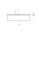
このような多光子吸収を利用するレーザ加工の原理について、図1〜図6を参照して説明する。図1はレーザ加工中の基板1の平面図であり、図2は図1に示す基板1のII−II線に沿った断面図であり、図3はレーザ加工後の基板1の平面図であり、図4は図3に示す基板1のIV−IV線に沿った断面図であり、図5は図3に示す基板1のV−V線に沿った断面図であり、図6は切断された基板1の平面図である。 The principle of laser processing using such multiphoton absorption will be described with reference to FIGS. 1 is a plan view of the
図1及び図2に示すように、基板1には、所望の切断予定ライン5が設定される。切断予定ライン5は直線状に延びた仮想線であり、本実施形態ではウェハを複数のチップに分割する際の各チップ間の境界線である。なお、ウェハに実際に線を引いて切断予定ライン5としてもよい。本実施形態では、多光子吸収が生じる条件で基板1の内部に集光点Pを合わせた上でレーザ光Lを照射し、改質領域7を形成する。なお、集光点Pとはレーザ光Lが集光した箇所のことである。 As shown in FIGS. 1 and 2, a desired
レーザ光Lを切断予定ライン5に沿って(すなわち矢印A方向に沿って)相対的に移動させることにより、集光点Pを切断予定ライン5に沿って移動させる。これにより、図3〜図5に示すように改質領域7が切断予定ライン5に沿って基板1の内部にのみ形成され、この改質領域7でもって切断起点領域8が形成される。このレーザ加工方法は、基板1がレーザ光Lを吸収することにより基板1を発熱させて改質領域7を形成するのではない。基板1にレーザ光Lを透過させ基板1の内部に多光子吸収を発生させて改質領域7を形成している。よって、基板1の表面3ではレーザ光Lがほとんど吸収されないので、基板1の表面3が溶融することはない。 The condensing point P is moved along the
基板1の切断において、切断する箇所に起点があると基板1はその起点から割れるので、図6に示すように比較的小さな力で基板1を切断することができる。よって、基板1の表面3にチッピングなどの不必要な割れを発生させることなく、かつ効率的に基板1の切断が可能となる。 In the cutting of the
なお、切断起点領域を起点とした基板の切断には、次の2通りが考えられる。1つは、切断起点領域形成後、基板に人為的な力が印加されることにより、切断起点領域を起点として基板が割れ、基板が切断される場合である。これは、例えば基板の厚さが大きい場合の切断である。人為的な力が印加されるとは、例えば、基板の切断起点領域に沿って基板に曲げ応力やせん断応力を加えたり、基板に温度差を与えることにより熱応力を発生させたりすることである。他の1つは、切断起点領域を形成することにより、切断起点領域を起点として基板の断面方向(厚さ方向)に向かって自然に割れ、結果的に基板が切断される場合である。これは、例えば基板の厚さが小さい場合には、1列の改質領域により切断起点領域が形成されることで可能となり、基板の厚さが大きい場合には、厚さ方向に複数列形成された改質領域により切断起点領域が形成されることで可能となる。なお、この自然に割れる場合も、切断する箇所において、切断起点領域が形成されていない部位に対応する部分の表面上にまで割れが先走ることがなく、切断起点領域を形成した部位に対応する部分のみを割断することができるので、割断を制御よくすることができる。近年、ウェハの基板などの基板の厚さは薄くなる傾向にあるので、このような制御性のよい割断方法は大変有効である。 Note that the following two types of cutting of the substrate starting from the cutting start region can be considered. One is a case where after the cutting start region is formed, an artificial force is applied to the substrate, so that the substrate is cracked from the cutting start region and the substrate is cut. This is cutting when the thickness of the substrate is large, for example. The artificial force is applied, for example, by applying a bending stress or a shear stress to the substrate along the cutting start region of the substrate, or generating a thermal stress by giving a temperature difference to the substrate. . The other one is a case where by forming the cutting start region, the substrate is naturally cracked in the cross-sectional direction (thickness direction) of the substrate starting from the cutting start region, resulting in the substrate being cut. For example, when the substrate thickness is small, the cutting start region is formed by one row of modified regions, and when the substrate thickness is large, multiple rows are formed in the thickness direction. This can be achieved by forming a cutting start region by the modified region. In addition, even when this breaks naturally, in the part to be cut, the part corresponding to the part where the cutting starting point region is formed without cracking ahead on the surface of the part corresponding to the part where the cutting starting point region is not formed Since it is possible to cleave only, the cleaving can be controlled well. In recent years, since the thickness of a substrate such as a wafer substrate tends to be thin, such a cleaving method with good controllability is very effective.
さて、本実施形態において多光子吸収により形成される改質領域としては、次の(1)〜(3)がある。 In the present embodiment, the modified regions formed by multiphoton absorption include the following (1) to (3).
(1)改質領域が1つ又は複数のクラックを含むクラック領域の場合
例えばサファイアやガラスなどからなる基板の内部に集光点を合わせて、集光点における電界強度が1×10⁸(W/cm2)以上で且つパルス幅が1μs以下の条件でレーザ光を照射する。このパルス幅の大きさは、多光子吸収を生じさせつつ基板の表面に余計なダメージを与えずに、基板の内部にのみクラック領域を形成できる条件である。これにより、基板の内部には多光子吸収による光学的損傷という現象が発生する。この光学的損傷により基板の内部に熱ひずみが誘起され、これにより基板の内部にクラック領域が形成される。電界強度の上限値としては、例えば1×1012(W/cm2)である。パルス幅は例えば1ns〜200nsが好ましい。(1) In the case where the modified region is a crack region including one or a plurality of cracks For example, the focusing point is set inside a substrate made of sapphire or glass, and the electric field strength at the focusing point is 1 × 10⁸ (W / Cm2 ) and the pulse width is 1 μs or less. The magnitude of this pulse width is a condition under which a crack region can be formed only inside the substrate without causing extra damage to the surface of the substrate while causing multiphoton absorption. As a result, a phenomenon of optical damage due to multiphoton absorption occurs inside the substrate. This optical damage induces thermal strain inside the substrate, thereby forming a crack region inside the substrate. The upper limit value of the electric field strength is, for example, 1 × 10¹² (W / cm2 ). The pulse width is preferably 1 ns to 200 ns, for example.
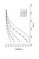
本発明者は、電界強度とクラックの大きさとの関係を実験により求めた。実験条件は次ぎの通りである。
(A)基板:パイレックス(登録商標)ガラス(厚さ700μm)
(B)レーザ
光源:半導体レーザ励起Nd:YAGレーザ
波長:1064nm
レーザ光スポット断面積:3.14×10⁻⁸cm2
発振形態:Qスイッチパルス
繰り返し周波数:100kHz
パルス幅:30ns
出力:出力<1mJ/パルス
レーザ光品質:TEM00
偏光特性:直線偏光
(C)集光用レンズ
レーザ光波長に対する透過率:60パーセント
(D)基板が載置される載置台の移動速度:100mm/秒The inventor obtained the relationship between the electric field strength and the size of the cracks by experiment. The experimental conditions are as follows.
(A) Substrate: Pyrex (registered trademark) glass (thickness 700 μm)
(B) Laser
Light source: Semiconductor laser pumped Nd: YAG laser
Wavelength: 1064nm
Laser beam spot cross-sectional area: 3.14 × 10⁻⁸ cm2
Oscillation form: Q switch pulse
Repeat frequency: 100 kHz
Pulse width: 30ns
Output: Output <1mJ / pulse
Laser light quality: TEM00
Polarization characteristics: Linearly polarized light (C) Condensing lens
Transmittance with respect to wavelength of laser beam: 60% (D) Moving speed of mounting table on which substrate is mounted: 100 mm / second
なお、レーザ光品質がTEM00とは、集光性が高くレーザ光の波長程度まで集光可能を意味する。Note that the laser light quality TEM00 means that the light condensing property is high and the light can be condensed to the wavelength of the laser light.
図7は上記実験の結果を示すグラフである。横軸はピークパワー密度であり、レーザ光がパルスレーザ光なので電界強度はピークパワー密度で表される。縦軸は1パルスのレーザ光により基板の内部に形成されたクラック部分(クラックスポット)の大きさを示している。クラックスポットが集まりクラック領域となる。クラックスポットの大きさは、クラックスポットの形状のうち最大の長さとなる部分の大きさである。グラフ中の黒丸で示すデータは集光用レンズ(C)の倍率が100倍、開口数(NA)が0.80の場合である。一方、グラフ中の白丸で示すデータは集光用レンズ(C)の倍率が50倍、開口数(NA)が0.55の場合である。ピークパワー密度が1011(W/cm2)程度から基板の内部にクラックスポットが発生し、ピークパワー密度が大きくなるに従いクラックスポットも大きくなることが分かる。FIG. 7 is a graph showing the results of the experiment. The horizontal axis represents the peak power density. Since the laser beam is a pulsed laser beam, the electric field strength is represented by the peak power density. The vertical axis indicates the size of a crack portion (crack spot) formed inside the substrate by one pulse of laser light. Crack spots gather to form a crack region. The size of the crack spot is the size of the portion having the maximum length in the shape of the crack spot. Data indicated by black circles in the graph is for the case where the magnification of the condenser lens (C) is 100 times and the numerical aperture (NA) is 0.80. On the other hand, the data indicated by the white circles in the graph is when the magnification of the condenser lens (C) is 50 times and the numerical aperture (NA) is 0.55. It can be seen that crack spots are generated inside the substrate from the peak power density of about 1011 (W / cm2 ), and the crack spots increase as the peak power density increases.
次に、上記したレーザ加工方法において、クラック領域形成による基板の切断のメカニズムについて図8〜図11を用いて説明する。図8に示すように、多光子吸収が生じる条件で基板1の内部に集光点Pを合わせてレーザ光Lを基板1に照射して切断予定ラインに沿って内部にクラック領域9を形成する。クラック領域9は1つ又は複数のクラックを含む領域である。このクラック領域9でもって切断起点領域が形成される。図9に示すようにクラック領域9を起点として(すなわち、切断起点領域を起点として)クラックがさらに成長し、図10に示すようにクラックが基板1の表面3と裏面21に到達し、図11に示すように基板1が割れることにより基板1が切断される。基板の表面と裏面に到達するクラックは自然に成長する場合もあるし、基板に力が印加されることにより成長する場合もある。 Next, in the laser processing method described above, a mechanism for cutting the substrate by forming a crack region will be described with reference to FIGS. As shown in FIG. 8, under the condition that multiphoton absorption occurs, the condensing point P is aligned inside the
(2)改質領域が溶融処理領域の場合
例えばシリコンのような半導体材料からなる基板の内部に集光点を合わせて、集光点における電界強度が1×10⁸(W/cm2)以上で且つパルス幅が1μs以下の条件でレーザ光を照射する。これにより基板の内部は多光子吸収によって局所的に加熱される。この加熱により基板の内部に溶融処理領域が形成される。溶融処理領域とは一旦溶融後再固化した領域や、まさに溶融状態の領域や、溶融状態から再固化する状態の領域であり、相変化した領域や結晶構造が変化した領域ということもできる。また、溶融処理領域とは単結晶構造、非晶質構造、多結晶構造において、ある構造が別の構造に変化した領域ということもできる。つまり、例えば、単結晶構造から非晶質構造に変化した領域、単結晶構造から多結晶構造に変化した領域、単結晶構造から非晶質構造及び多結晶構造を含む構造に変化した領域を意味する。基板がシリコン単結晶構造の場合、溶融処理領域は例えば非晶質シリコン構造である。電界強度の上限値としては、例えば1×1012(W/cm2)である。パルス幅は例えば1ns〜200nsが好ましい。また、シリコンに限らず、例えばサファイアなどにおいても上記した溶融処理領域を形成することが可能である。(2) When the modified region is a melt-processed region For example, the focusing point is set inside a substrate made of a semiconductor material such as silicon, and the electric field strength at the focusing point is 1 × 10⁸ (W / cm2 ) or more In addition, the laser beam is irradiated under the condition that the pulse width is 1 μs or less. As a result, the inside of the substrate is locally heated by multiphoton absorption. By this heating, a melt processing region is formed inside the substrate. The melt treatment region is a region once solidified after melting, a region in a molten state, or a region re-solidified from a molten state, and can also be referred to as a phase-changed region or a region in which the crystal structure has changed. The melt treatment region can also be said to be a region in which one structure is changed to another structure in a single crystal structure, an amorphous structure, or a polycrystalline structure. In other words, for example, a region changed from a single crystal structure to an amorphous structure, a region changed from a single crystal structure to a polycrystalline structure, or a region changed from a single crystal structure to a structure including an amorphous structure and a polycrystalline structure. To do. When the substrate has a silicon single crystal structure, the melt processing region has, for example, an amorphous silicon structure. The upper limit value of the electric field strength is, for example, 1 × 10¹² (W / cm2 ). The pulse width is preferably 1 ns to 200 ns, for example. Moreover, it is possible to form the above-described melt processing region not only in silicon but also in sapphire, for example.
本発明者は、シリコンウェハの内部で溶融処理領域が形成されることを実験により確認した。実験条件は次の通りである。
(A)基板:シリコンウェハ(厚さ350μm、外径4インチ)
(B)レーザ
光源:半導体レーザ励起Nd:YAGレーザ
波長:1064nm
レーザ光スポット断面積:3.14×10⁻⁸cm2
発振形態:Qスイッチパルス
繰り返し周波数:100kHz
パルス幅:30ns
出力:20μJ/パルス
レーザ光品質:TEM00
偏光特性:直線偏光
(C)集光用レンズ
倍率:50倍
N.A.:0.55
レーザ光波長に対する透過率:60パーセント
(D)基板が載置される載置台の移動速度:100mm/秒The inventor has confirmed through experiments that a melt-processed region is formed inside a silicon wafer. The experimental conditions are as follows.
(A) Substrate: Silicon wafer (thickness 350 μm,
(B) Laser
Light source: Semiconductor laser pumped Nd: YAG laser
Wavelength: 1064nm
Laser beam spot cross-sectional area: 3.14 × 10⁻⁸ cm2
Oscillation form: Q switch pulse
Repeat frequency: 100 kHz
Pulse width: 30ns
Output: 20μJ / pulse
Laser light quality: TEM00
Polarization characteristics: Linearly polarized light (C) Condensing lens
Magnification: 50 times
N. A. : 0.55
Transmittance with respect to wavelength of laser beam: 60% (D) Moving speed of mounting table on which substrate is mounted: 100 mm / second
図12は、上記条件でのレーザ加工により切断されたシリコンウェハの一部における断面の写真を表した図である。シリコンウェハ11の内部に溶融処理領域13が形成されている。なお、上記条件により形成された溶融処理領域13の厚さ方向の大きさは100μm程度である。 FIG. 12 is a view showing a photograph of a cross section of a part of a silicon wafer cut by laser processing under the above conditions. A
溶融処理領域13が多光子吸収により形成されたことを説明する。図13は、レーザ光の波長とシリコン基板の内部の透過率との関係を示すグラフである。ただし、シリコン基板の表面側と裏面側それぞれの反射成分を除去し、内部のみの透過率を示している。シリコン基板の厚さtが50μm、100μm、200μm、500μm、1000μmの各々について上記関係を示した。 The fact that the
例えば、Nd:YAGレーザの波長である1064nmにおいて、シリコン基板の厚さが500μm以下の場合、シリコン基板の内部ではレーザ光が80%以上透過することが分かる。図12に示すシリコンウェハ11の厚さは350μmなので、多光子吸収による溶融処理領域13はシリコンウェハの中心付近、つまり表面から175μmの部分に形成される。この場合の透過率は、厚さ200μmのシリコンウェハを参考にすると、90%以上なので、レーザ光がシリコンウェハ11の内部で吸収されるのは僅かであり、ほとんどが透過する。このことは、シリコンウェハ11の内部でレーザ光が吸収されて、溶融処理領域13がシリコンウェハ11の内部に形成(つまりレーザ光による通常の加熱で溶融処理領域が形成)されたものではなく、溶融処理領域13が多光子吸収により形成されたことを意味する。 For example, when the thickness of the silicon substrate is 500 μm or less at the wavelength of the Nd: YAG laser of 1064 nm, it can be seen that the laser light is transmitted by 80% or more inside the silicon substrate. Since the thickness of the
なお、シリコンウェハは、溶融処理領域でもって形成される切断起点領域を起点として断面方向に向かって割れを発生させ、その割れがシリコンウェハの表面と裏面とに到達することにより、結果的に切断される。シリコンウェハの表面と裏面に到達するこの割れは自然に成長する場合もあるし、シリコンウェハに力が印加されることにより成長する場合もある。なお、切断起点領域からシリコンウェハの表面と裏面とに割れが自然に成長する場合には、切断起点領域を形成する溶融処理領域が溶融している状態から割れが成長する場合と、切断起点領域を形成する溶融処理領域が溶融している状態から再固化する際に割れが成長する場合とのいずれもある。ただし、どちらの場合も溶融処理領域はシリコンウェハの内部のみに形成され、切断後の切断面には、図12のように内部にのみ溶融処理領域が形成されている。基板の内部に溶融処理領域でもって切断起点領域を形成すると、割断時、切断起点領域ラインから外れた不必要な割れが生じにくいので、割断制御が容易となる。 Silicon wafers are cracked in the cross-sectional direction starting from the cutting start region formed by the melt processing region, and the cracks reach the front and back surfaces of the silicon wafer, resulting in cutting. Is done. The cracks that reach the front and back surfaces of the silicon wafer may grow naturally or may grow by applying force to the silicon wafer. In addition, when a crack naturally grows from the cutting start region to the front and back surfaces of the silicon wafer, the case where the crack grows from a state where the melt treatment region forming the cutting starting region is melted, and the cutting starting region There are both cases where cracks grow when the solidified region is melted from the molten state. However, in either case, the melt processing region is formed only inside the silicon wafer, and the melt processing region is formed only inside the cut surface after cutting as shown in FIG. If the cutting start region is formed in the substrate by the melt processing region, unnecessary cracking off the cutting start region line is unlikely to occur during cleaving, so that cleaving control is facilitated.
(3)改質領域が屈折率変化領域の場合
例えばガラスなどからなる基板の内部に集光点を合わせて、集光点における電界強度が1×10⁸(W/cm2)以上で且つパルス幅が1ns以下の条件でレーザ光を照射する。パルス幅を極めて短くして、多光子吸収を基板の内部に起こさせると、多光子吸収によるエネルギーが熱エネルギーに転化せずに、基板の内部にはイオン価数変化、結晶化又は分極配向等の永続的な構造変化が誘起されて屈折率変化領域が形成される。電界強度の上限値としては、例えば1×1012(W/cm2)である。パルス幅は例えば1ns以下が好ましく、1ps以下がさらに好ましい。(3) When the modified region is a refractive index changing region For example, a focusing point is set inside a substrate made of glass or the like, the electric field intensity at the focusing point is 1 × 10⁸ (W / cm2 ) or more, and a pulse Laser light is irradiated under conditions where the width is 1 ns or less. When the pulse width is made extremely short and multiphoton absorption occurs inside the substrate, the energy due to the multiphoton absorption is not converted into thermal energy, and the ionic valence change, crystallization, polarization orientation, etc. are inside the substrate. A permanent structural change is induced to form a refractive index changing region. The upper limit value of the electric field strength is, for example, 1 × 10¹² (W / cm2 ). For example, the pulse width is preferably 1 ns or less, and more preferably 1 ps or less.
以上、多光子吸収により形成される改質領域として(1)〜(3)の場合を説明したが、基板の結晶構造やその劈開性などを考慮して切断起点領域を次のように形成すれば、その切断起点領域を起点として、より一層小さな力で、しかも精度良く基板を切断することが可能になる。 As described above, the cases of (1) to (3) have been described as the modified regions formed by multiphoton absorption. However, the cutting starting region is formed as follows in consideration of the crystal structure of the substrate and its cleavage property. For example, the substrate can be cut with a smaller force and with higher accuracy from the cutting start region.
すなわち、シリコンなどのダイヤモンド構造の単結晶半導体からなる基板の場合は、(111)面(第1劈開面)や(110)面(第2劈開面)に沿った方向に切断起点領域を形成するのが好ましい。また、GaAsなどの閃亜鉛鉱型構造のIII−V族化合物半導体からなる基板の場合は、(110)面に沿った方向に切断起点領域を形成するのが好ましい。さらに、サファイアなどの六方晶系の結晶構造を有する基板の場合は、(0001)面(C面)を主面として(1120)面(A面)或いは(1100)面(M面)に沿った方向に切断起点領域を形成するのが好ましい。 That is, in the case of a substrate made of a single crystal semiconductor having a diamond structure such as silicon, the cutting start region is formed in a direction along the (111) plane (first cleavage plane) or the (110) plane (second cleavage plane). Is preferred. In the case of a substrate made of a zinc-blende-type III-V group compound semiconductor such as GaAs, it is preferable to form the cutting start region in the direction along the (110) plane. Further, in the case of a substrate having a hexagonal crystal structure such as sapphire, the (0001) plane (C plane) is the main plane and the (1120) plane (A plane) or (1100) plane (M plane) is taken along. It is preferable to form the cutting start region in the direction.
なお、上述した切断起点領域を形成すべき方向(例えば、単結晶シリコン基板における(111)面に沿った方向)、或いは切断起点領域を形成すべき方向に直交する方向に沿って基板にオリエンテーションフラット(後述)を形成すれば、そのオリエンテーションフラットを基準とすることで、切断起点領域を容易且つ正確に基板に形成することが可能になる。 Note that the orientation flat is formed on the substrate along the direction in which the above-described cutting start region is to be formed (for example, the direction along the (111) plane in the single crystal silicon substrate) or the direction perpendicular to the direction in which the cutting start region is to be formed. If (described later) is formed, it is possible to easily and accurately form the cutting start region on the substrate by using the orientation flat as a reference.
次に、上述したレーザ加工方法に使用されるレーザ加工装置について、図14を参照して説明する。図14はレーザ加工装置100の概略構成図である。 Next, a laser processing apparatus used in the laser processing method described above will be described with reference to FIG. FIG. 14 is a schematic configuration diagram of the
レーザ加工装置100は、レーザ光Lを発生するレーザ光源101と、レーザ光Lの出力やパルス幅等を調節するためにレーザ光源101を制御するレーザ光源制御部102と、レーザ光Lの反射機能を有しかつレーザ光Lの光軸の向きを90°変えるように配置されたダイクロイックミラー103と、ダイクロイックミラー103で反射されたレーザ光Lを集光する集光用レンズ105と、集光用レンズ105で集光されたレーザ光Lが照射されるウェハ2が載置される載置台107と、載置台107をX軸方向に移動させるためのX軸ステージ109と、載置台107をX軸方向に直交するY軸方向に移動させるためのY軸ステージ111と、載置台107をX軸及びY軸方向に直交するZ軸方向に移動させるためのZ軸ステージ113と、これら3つのステージ109,111,113の移動を制御するステージ制御部115とを備える。 The
この集光点PのX(Y)軸方向の移動は、基板1をX(Y)軸ステージ109(111)によりX(Y)軸方向に移動させることにより行う。Z軸方向は、ウェハ2の表面4と直交する方向なので、ウェハ2に入射するレーザ光Lの焦点深度の方向となる。よって、Z軸ステージ113をZ軸方向に移動させることにより、ウェハ2の基板の内部にレーザ光Lの集光点Pを合わせることができる。これにより、レーザ光入射面から所定距離内側の所望の位置に集光点Pを合わせることができる。 The converging point P is moved in the X (Y) axis direction by moving the
レーザ光源101はパルスレーザ光を発生するNd:YAGレーザである。レーザ光源101に用いることができるレーザとして、この他、Nd:YVO4レーザ、Nd:YLFレーザやチタンサファイアレーザがある。本実施形態では、基板1の加工にパルスレーザ光を用いているが、多光子吸収を起こさせることができるなら連続波レーザ光でもよい。The
レーザ加工装置100はさらに、載置台107に載置されたウェハ2を可視光線により照明するために可視光線を発生する観察用光源117と、ダイクロイックミラー103及び集光用レンズ105と同じ光軸上に配置された可視光用のビームスプリッタ119とを備える。ビームスプリッタ119と集光用レンズ105との間にダイクロイックミラー103が配置されている。ビームスプリッタ119は、可視光線の約半分を反射し残りの半分を透過する機能を有しかつ可視光線の光軸の向きを90°変えるように配置されている。観察用光源117から発生した可視光線はビームスプリッタ119で約半分が反射され、この反射された可視光線がダイクロイックミラー103及び集光用レンズ105を透過し、ウェハ2の切断予定ライン5等を含む表面4を照明する。なお、ウェハ2の裏面が集光用レンズ105側となるようウェハ2が載置台107に載置された場合は、ここでいう「表面」が「裏面」となるのは勿論である。 The
レーザ加工装置100はさらに、ビームスプリッタ119、ダイクロイックミラー103及び集光用レンズ105と同じ光軸上に配置された撮像素子121及び結像レンズ123を備える。撮像素子121としては例えばCCDカメラがある。切断予定ライン5等を含むウェハ2の表面4を照明した可視光線の反射光は、集光用レンズ105、ダイクロイックミラー103、ビームスプリッタ119を透過し、結像レンズ123で結像されて撮像素子121で撮像され、撮像データとなる。 The
レーザ加工装置100はさらに、撮像素子121から出力された撮像データが入力される撮像データ処理部125と、レーザ加工装置100全体を制御する全体制御部127と、モニタ129とを備える。撮像データ処理部125は、撮像データを基にして観察用光源117で発生した可視光の焦点をウェハ2の表面4上に合わせるための焦点データを演算する。この焦点データを基にしてステージ制御部115がZ軸ステージ113を移動制御することにより、可視光の焦点がウェハ2の表面4に合うようにする。よって、撮像データ処理部125はオートフォーカスユニットとして機能する。また、撮像データ処理部125は、撮像データを基にして表面4の拡大画像等の画像データを演算する。この画像データは全体制御部127に送られ、全体制御部で各種処理がなされ、モニタ129に送られる。これにより、モニタ129に拡大画像等が表示される。 The
全体制御部127には、ステージ制御部115からのデータ、撮像データ処理部125からの画像データ等が入力し、これらのデータも基にしてレーザ光源制御部102、観察用光源117及びステージ制御部115を制御することにより、レーザ加工装置100全体を制御する。よって、全体制御部127はコンピュータユニットとして機能する。 Data from the
次に、上述したレーザ加工方法及びレーザ加工装置100を用いた、本実施形態に係る発光素子の製造方法について説明する。図15は、本実施形態に係る発光素子の製造方法において用いられるウェハ2を示す斜視図である。また、図16は、図15に示されたウェハ2の平面図である。また、図17は、図16に示されたウェハ2のVI−VI断面及びVII−VII断面を示す拡大図である。本実施形態では、発光素子として発光ダイオードを製造する方法について説明する。 Next, a method for manufacturing the light emitting element according to this embodiment using the laser processing method and the
図15〜図17を参照すると、ウェハ2は、略円盤状を呈しており、オリエンテーションフラット(以下「OF」という)19を有している。本実施形態において、ウェハ2は、サファイアからなる基板1と、基板1の表面3上に積層された第1導電型半導体層であるn型半導体層17aと、n型半導体層17a上に積層された第2導電型半導体層であるp型半導体層17bとを備えている。n型半導体層17a及びp型半導体層17bは、例えばGaNなどのIII−V族化合物半導体からなり、互いにpn接合されている。基板1が厚いとn型半導体層17a及びp型半導体層17bにおける発熱を逃がすことが困難となるので、基板1の厚さは50μm〜200μm、好ましくは50μm〜150μmである。また、n型半導体層17a及びp型半導体層17bの厚さは、それぞれ例えば6μm、1μmである。 15 to 17, the
また、図16を参照すると、ウェハ2には切断予定ライン5が設定されている。切断予定ライン5は、ウェハ2をチップ状に切断するために想定される。本実施形態では、切断予定ライン5はOF19の長手方向に平行な方向と、OF19に垂直な方向とにそれぞれ複数設定されている。また、前述したように、OF19は、サファイアからなる基板1の劈開面に沿った方向、或いは劈開面に沿った方向と直交する方向に形成されている。すなわち、切断予定ライン5の少なくとも一方向は、サファイアからなる基板1の(1120)面(A面)或いは(1100)面(M面)に沿った方向に設定されている。なお、互いに隣り合う切断予定ライン5の間隔は、例えば2mm程度である。 Further, referring to FIG. 16, a scheduled
図18及び図19は、本実施形態に係る発光素子の製造方法を説明するためのフローチャートである。また、図20〜図23は、発光素子の製造方法を説明するためのウェハ2の断面図である。 18 and 19 are flowcharts for explaining the method for manufacturing the light emitting device according to this embodiment. 20-23 is sectional drawing of the
図18を参照すると、まず、ウェハ2の裏面(すなわち、基板1の裏面21)にエキスパンドテープ23を貼る(S1、図20)。エキスパンドテープ23は、例えば加熱により伸びる材料からなり、後の工程において、ウェハ2をチップ状に分離させるために用いられる。 Referring to FIG. 18, first, expand
続いて、図16に示された切断予定ライン5に沿ってウェハ2のp型半導体層17b側の面をエッチングすることにより、溝25を形成する(S3、図21)。このとき、溝25の深さが、p型半導体層17bからn型半導体層17aの途中までの深さとなるように溝25を形成する。また、溝25の幅を、p型半導体層17bが所望の形状寸法となるように形成するとともに、ウェハ2をチップ状に分離した後の溝25の底面上にn型半導体層17aと電気的に接続される電極を設けるスペースを確保できるように形成する。また、このとき、溝25の底面を、平坦かつ滑面に形成することが好ましい。なぜなら、後の工程において溝25の底面をレーザ光入射面として基板1内部へレーザ光を照射するが、溝25の底面が粗いと、レーザ光が底面において散乱してしまい基板1の内部に入射するレーザ光が適切な強度にならないためである。 Subsequently, the
なお、エッチング方法にはウェットエッチング及びドライエッチングがあるが、溝25を形成する際にはそのいずれを用いてもよい。ウェットエッチングとしては例えばリン酸及び硫酸の混酸によるエッチングがある。また、ドライエッチングとしては例えば反応性イオンエッチング(RIE)、反応性イオンビームエッチング(RIB)、イオンミリング等がある。また、溝25を形成する際には、エッチング以外にも例えばブレードダイシング等により形成してもよい。 Etching methods include wet etching and dry etching, and any of them may be used when forming the
続いて、ウェハ2の基板1の内部に、溝25に沿って切断起点領域を形成する(S5、図22)。すなわち、溝25の底面をレーザ光入射面としてn型半導体層17aを介して基板1の内部の集光点Pへレーザ光Lを照射することにより、基板1の内部に改質領域7を形成する。この改質領域7が、ウェハ2を切断する際の切断起点領域となる。 Subsequently, a cutting start region is formed along the
ここで、図19は、図14に示されたレーザ加工装置100を用いてウェハ2に切断起点領域を形成する方法を示すフローチャートである。なお、本実施形態において、ウェハ2は、レーザ加工装置100の載置台107に、ウェハ2のp型半導体層17b側の面が集光用レンズ105と対向するように配置される。すなわち、レーザ光Lは、ウェハ2のp型半導体層17b側から入射される。 Here, FIG. 19 is a flowchart showing a method of forming a cutting start region on the
図14及び図19を参照すると、まず、基板1及びn型半導体層17aの光吸収特性を図示しない分光光度計等により測定する。この測定結果に基づいて、基板1及びn型半導体層17aに対して透明な波長又は吸収の少ない波長のレーザ光Lを発生するレーザ光源101を選定する(S101)。なお、このレーザ光Lはウェハ2のp型半導体層17b側から照射されることとなるため、ウェハ2の裏面21に例えば遮光性の電極等が設けられている場合であっても、レーザ加工の妨げとなるようなことはない。 14 and 19, first, the light absorption characteristics of the
続いて、基板1及びn型半導体層17aの厚さ、材質、及び屈折率等を考慮して、ウェハ2のZ軸方向の移動量を決定する(S103)。これは、溝25の底面から所定距離内側の所望の位置にレーザ光Lの集光点Pを合わせるために、溝25の底面に位置するレーザ光Lの集光点Pを基準としたウェハ2のZ軸方向の移動量である。この移動量は全体制御部127に入力される。 Subsequently, the amount of movement of the
ウェハ2をレーザ加工装置100の載置台107にウェハ2の表面4が集光用レンズ105側と対向するよう載置する。そして、観察用光源117から可視光を発生させてウェハ2の表面4を照明する(S105)。照明されたウェハ2における溝25の底面を撮像素子121により撮像する。撮像素子121により撮像された撮像データは撮像データ処理部125に送られる。この撮像データに基づいて撮像データ処理部125は、観察用光源117の可視光の焦点がウェハ2の溝25の底面に位置するような焦点データを演算する(S107)。 The
この焦点データはステージ制御部115に送られる。ステージ制御部115は、この焦点データを基にしてZ軸ステージ113をZ軸方向の移動させる(S109)。これにより、観察用光源117の可視光の焦点がウェハ2の溝25の底面に位置する。なお、撮像データ処理部125は撮像データに基づいて、溝25を含むウェハ2の表面4の拡大画像データを演算する。この拡大画像データは全体制御部127を介してモニタ129に送られ、これによりモニタ129に溝25付近の拡大画像が表示される。 This focus data is sent to the
全体制御部127には予めステップS103で決定された移動量データが入力されており、この移動量データがステージ制御部115に送られる。ステージ制御部115はこの移動量データに基づいて、レーザ光Lの集光点Pの位置が基板1の内部であって溝25の底面から所定距離内側となるように、Z軸ステージ113によりウェハ2をZ軸方向に移動させる(S111)。 The movement amount data determined in advance in step S <b> 103 is input to the
続いて、レーザ光源101からレーザ光Lを発生させて、レーザ光Lをウェハ2の溝25の底面に照射する。レーザ光Lの集光点Pは基板1の内部に位置しているので、改質領域7は基板1の内部にのみ形成される。また、このとき、レーザ光Lを溝25の幅よりも狭い範囲に入射して、溝25の長手方向と交差する方向の改質領域7の幅を、溝25の当該方向の幅よりも狭く形成することが好ましい。なお、レーザ光Lをこのように入射するためには、溝25の底面におけるレーザ光Lの屈折率、溝25の幅、及び基板1内部の集光点Pの位置を互いに調整する必要がある。 Subsequently, laser light L is generated from the
続いて、溝25に沿うようにX軸ステージ109やY軸ステージ111を移動させて、溝25に沿うように改質領域7を複数形成するか、あるいは溝25の長手方向に連続して形成し、切断予定ライン5に沿う切断起点領域を基板1の内部に形成する(S113)。 Subsequently, the
ここで、再び図18を参照すると、ウェハ2の基板1に切断起点領域を形成したのち、切断起点領域に沿ってウェハ2を複数のチップに切断する(S7、図23)。すなわち、エキスパンドテープ23をウェハ2の裏面21と平行な方向に伸ばすことにより、基板1の内部に形成された切断起点領域を起点として基板1が切断される。このとき、一般的にn型半導体層17aは基板1よりも充分に薄いので、基板1が切断されると同時に、溝25の底面と基板1との間にあるn型半導体層17aが切断される。このようにしてウェハ2が切断され、複数のチップ状に分割される。こうして、n型半導体層17a及びp型半導体層17bとの間にpn接合を有する発光ダイオード31が形成される。なお、発光ダイオード31に残っている溝25の底面には、必要に応じてn型半導体層17aに電気的に接続される電極を設けることができる。 Here, referring to FIG. 18 again, after the cutting start region is formed on the
以上説明したように、本実施形態に係る発光素子の製造方法及び発光ダイオードでは、ウェハ2の基板1の内部に多光子吸収という現象により形成される改質領域7でもって、切断予定ライン5に沿った切断起点領域を形成することができ、基板1を切断起点領域に沿って比較的小さな力で割って切断することができる。そして、基板1が切断予定ライン5に沿って切断されることにより、基板1上に積層されたIII−V族化合物からなるn型半導体層17aも切断予定ラインに沿って切断される。したがって、この製造方法によれば、n型半導体層17aなどのIII−V族化合物半導体層を有するウェハ2を高精度かつ効率よく切断することができる。 As described above, in the method for manufacturing a light emitting device and the light emitting diode according to the present embodiment, the
また、ウェハを切断する際にブレードダイシング法のみを用いる場合、切断中のウェハを洗浄するための大がかりな洗浄工程が必要となり、大型の設備が必要となる。これに対し、本実施形態に係る発光素子の製造方法によれば、ウェハ2の厚さの殆どを切断起点領域により切断するので、そのような洗浄工程は必要なく、発光素子を製造するための設備をより簡易にできる。 Further, when only the blade dicing method is used when cutting the wafer, a large-scale cleaning process for cleaning the wafer being cut is required, and a large facility is required. On the other hand, according to the method for manufacturing a light emitting element according to this embodiment, most of the thickness of the
また、本実施形態に係る発光素子の製造方法においては、基板1にレーザ光Lを照射する前に、切断予定ライン5に沿ってn型半導体層17a及びp型半導体層17bに溝25を形成することが好ましい。この製造方法によれば、ウェハ2を切断して形成される発光ダイオード31のn型半導体層17aに電極を設ける場合に、この電極を設けるためのスペースを容易に形成することができる。なお、溝25を形成しない場合には、基板1が切断起点領域に沿って切断される際に、n型半導体層17aに加えてp型半導体層17bも同時に切断される。 In the method for manufacturing the light emitting device according to this embodiment, the
また、本実施形態に係る発光素子の製造方法においては、基板1にレーザ光Lを照射する際に、溝25の底面をレーザ光入射面としている。この製造方法によれば、基板1にレーザ光Lを照射する際に、ウェハ2上に想定された切断予定ライン5を容易に認識することができるとともに、レーザ光Lを溝25の位置にあわせて精度良く照射することができる。 Further, in the method for manufacturing the light emitting element according to the present embodiment, when the
また、本実施形態に係る発光素子の製造方法においては、ウェハ2に溝25を形成する際に、溝25の底面を平坦かつ滑面に形成することが好ましい。これによって、溝25の底面をレーザ光入射面とする場合に、溝25の底面におけるレーザ光Lの散乱を防ぐことができる。 Further, in the method for manufacturing the light emitting element according to the present embodiment, when the
また、本実施形態に係る発光素子の製造方法においては、改質領域7を形成する際に、溝25の長手方向と交差する方向の改質領域7の幅を、溝25の当該方向の幅よりも狭く形成している。この製造方法によれば、レーザ光Lを溝25の幅よりも狭い範囲に入射することで改質領域7を形成できるので、溝25の周囲のp型半導体層17bがレーザ光Lにより損傷することを防止できる。 In the method for manufacturing the light emitting device according to the present embodiment, when forming the modified
なお、基板1の裏面21をレーザ光入射面として、集光点Pにレーザ光Lを照射することにより、改質領域7を形成してもよい。このようにすれば、溝25の底面が粗いなどの理由によりレーザ光Lの入射に適さない場合であっても、ウェハ2の基板1の内部に改質領域7でもって切断起点領域を形成することができる。また、前述したように、レーザ光入射面は平坦かつ滑面であることが好ましいが、比較的狭い溝25の底面よりも、基板1の裏面21のほうが平坦かつ滑面に形成しやすい場合がある。このような場合に、基板1の裏面21を例えば研磨するなどしてからレーザ光Lを入射すれば、切断起点領域を容易に形成することができる。なお、このように基板1の裏面21からレーザ光Lを入射する場合は、エキスパンドテープ23をウェハ2の表面4に貼るとよい。 Note that the modified
図24は、本実施形態による発光素子の製造方法の変形例を説明するための断面図である。本変形例では、基板1の内部において、基板1の厚さ方向に複数の改質領域7を形成する。改質領域7をこのように形成するには、図19に示されたフローチャートのステップS111(ウェハをZ軸方向に移動)とステップS113(改質領域の形成)とを交互に複数回行うとよい。また、ウェハをZ軸方向に移動するのと改質領域の形成とを同時に行うことにより、基板1の厚さ方向に連続して改質領域7を形成してもよい。 FIG. 24 is a cross-sectional view illustrating a modification of the method for manufacturing the light emitting device according to the present embodiment. In this modification, a plurality of modified
本変形例のように改質領域7を形成することにより、基板1の厚さ方向に延びた切断起点領域を形成することができる。従って、ウェハ2をより小さな力で割って切断することができる。さらに、基板1の厚さ方向に改質領域7によるクラックを成長させれば、外部からの力を必要とせずウェハ2を分離することもできる。 By forming the modified
図25及び図26は、本実施形態による発光素子の製造方法の別の変形例を説明するための断面図である。本変形例では、発光素子として半導体レーザを製造する方法を説明する。 25 and 26 are cross-sectional views for explaining another variation of the method for manufacturing the light emitting device according to the present embodiment. In this modification, a method for manufacturing a semiconductor laser as a light emitting element will be described.
図25を参照すると、本変形例に用いられるウェハ2aは、サファイアからなる基板1と、基板1の表面3上に積層された第1導電型半導体層であるn型半導体層33aと、n型半導体層33a上に積層された活性層33bと、活性層33b上に積層された第2導電型半導体層であるp型半導体層33cとを備えている。本変形例において、n型半導体層33a、活性層33b、及びp型半導体層33cは、例えばGaNなどのIII−V族化合物半導体からなり、量子井戸構造を構成している。なお、本変形例におけるウェハ2aは、図15及び図16に示された上記実施形態のウェハ2と同様の外形を有している。 Referring to FIG. 25, a
本変形例による発光素子の製造方法では、まず、ウェハ2aの裏面21にエキスパンドテープ23を貼る。そして、ウェハ2aのp型半導体層33c側の面に溝25を形成する。このとき、溝25を、切断予定ライン5(図16参照)に沿って、活性層33bを分割して基板1に達しない深さ、すなわちp型半導体層33cからn型半導体層33aの途中までの深さになるように形成する。また、このとき、溝25の側壁によって、活性層33bに共振面35が形成される。共振面35は、活性層33bを挟んで2面形成され、この2面は互いに対向する。 In the method for manufacturing a light emitting device according to this modification, first, an expanded
続いて、溝25の底面をレーザ光入射面として基板1の内部の集光点Pにレーザ光Lを照射することにより、改質領域7を形成する。そして、この改質領域7を形成しながら溝25の長手方向に沿って集光点Pを移動することにより、基板1の内部に切断起点領域を形成する。そして、図26に示されるように、エキスパンドテープ23を伸ばすことにより、ウェハ2aを切断起点領域に沿ってチップ状に切断し、半導体レーザ素子37を得る。 Subsequently, the modified
本変形例により得られる半導体レーザ素子37においては、ウェハ2aの基板1の内部に多光子吸収という現象により形成される改質領域7でもって形成された、切断予定ライン5に沿った切断起点領域により基板1が切断起点領域に沿って比較的小さな力で割って切断される。そして、基板1が切断予定ライン5に沿って切断されることにより、基板1上に積層されたn型半導体層33aも切断予定ライン5に沿って切断される。したがって、III−V族化合物からなるn型半導体層33aを有するウェハ2が高精度かつ効率よく切断されて形成された半導体レーザ素子37を提供することができる。 In the
また、本変形例により得られる半導体レーザ素子37においては、活性層33bを分割するとともに基板1に達しない深さの溝25がウェハ2aに形成されることによって、n型半導体層33aと電気的に接続されるカソード電極のためのスペースが形成されるとともに、レーザ発振のための共振面35が活性層33bに形成される。なお、溝25を形成しない場合には、基板1が切断起点領域に沿って切断される際に、n型半導体層33aに加えて活性層33b及びp型半導体層33cも同時に切断される。 In the
以上、本発明の実施形態及び変形例について詳細に説明したが、本発明は上記実施形態及び変形例に限定されないことはいうまでもない。 As mentioned above, although embodiment and the modification of this invention were described in detail, it cannot be overemphasized that this invention is not limited to the said embodiment and modification.
上記実施形態及び変形例では、基板の材料としてサファイアを用いているが、これ以外にも、例えばSiC、Si、ZnO、AlN、及びGaAsなどを用いることができる。また、p型半導体層、活性層、及びn型半導体層の材料としてGaNを用いているが、これ以外にも、例えばGaAlAs、GaAlAsP、GaAlInPなどのIII−V族化合物を用いることができる。 In the embodiment and the modification, sapphire is used as the material of the substrate, but other than this, for example, SiC, Si, ZnO, AlN, GaAs, or the like can be used. Moreover, although GaN is used as the material of the p-type semiconductor layer, the active layer, and the n-type semiconductor layer, other than this, for example, a III-V group compound such as GaAlAs, GaAlAsP, and GaAlInP can be used.
また、III−V族化合物のなかでも例えばInXAlYGa1-X-YN(X≧0、Y≧0、X+Y≦1)で表されるような窒化物系III−V族化合物(GaNも含まれる)からなる半導体層は、一般的にサファイア基板上に積層されることが多い。サファイアは、他の材料にくらべて硬度が大きく、エッチングやブレードダイシングに要する時間が長くなる。しかも、サファイア及び窒化物系III−V族化合物は、GaAsなどに比べて劈開性が小さく、特許文献1などに開示されたダイヤモンドスクライブ法を用いると切断面が不規則になりやすい。従って、サファイア基板上に窒化物系III−V族化合物半導体が積層されたようなウェハにおいて、サファイア基板と半導体層とを同時に切断するような場合には、本発明による発光素子の製造方法を適用することにより、格段に切断精度がよくなるとともに製造効率を高めることができる。Further, among III-V compounds, for example, a nitride III-V compound (GaN is also represented by InX AlY Ga1-XY N (X ≧ 0, Y ≧ 0, X + Y ≦ 1)). In general, a semiconductor layer made up of (included) is often stacked on a sapphire substrate. Sapphire has a higher hardness than other materials, and takes longer time for etching and blade dicing. In addition, sapphire and nitride-based III-V group compounds are less cleaved than GaAs and the like, and if the diamond scribe method disclosed in
また、上記実施形態及び実施例における改質領域7形成以前に、基板が薄くなるよう裏面を研磨してもよい。図27(a)〜(c)は、上記した実施形態におけるウェハ2の基板1の裏面21を研磨する方法の一例を示す図である。まず、図27(a)に示されるように、ウェハ2のp型半導体層17b側の面にテープ24を貼る。そして、図27(b)に示されるように、基板1の裏面21を研磨して、基板1の厚さを小さくする。このとき、ウェハ2は裏面21側が上向いており、図27(b)は実際とは上下逆の図になっている。続いて、図27(c)に示されるように、テープ24を除去し、基板1の裏面21にエキスパンドテープ23を貼る。 Further, the back surface may be polished so that the substrate becomes thinner before the formation of the modified
基板が比較的薄い場合には、基板を切断する際の精度が一層向上する。さらに、基板の裏面からレーザ光を入射する場合、基板を薄くすることで溝の位置が裏面から確認できる。また、改質領域から基板の厚さ方向にクラックを成長させることにより、外部からの力を必要とせずウェハをチップに分離することも容易となる。 When the substrate is relatively thin, the accuracy in cutting the substrate is further improved. Furthermore, when laser light is incident from the back surface of the substrate, the position of the groove can be confirmed from the back surface by thinning the substrate. Further, by growing cracks from the modified region in the thickness direction of the substrate, it becomes easy to separate the wafer into chips without requiring external force.
また、上記実施形態及び実施例では、半導体層としてp型半導体層、活性層、及びn型半導体層が基板に積層されている。半導体層としてはこれ以外にも、電極との電気的接続のためのコンタクト層などがさらに積層されていてもよい。また、第1導電型をn型とし、第2導電型をp型としているが、第1導電型がp型で第2導電型がn型であってもよい。 Moreover, in the said embodiment and Example, the p-type semiconductor layer, the active layer, and the n-type semiconductor layer are laminated | stacked on the board | substrate as a semiconductor layer. In addition to this, a contact layer for electrical connection with the electrode may be further laminated as the semiconductor layer. Further, although the first conductivity type is n-type and the second conductivity type is p-type, the first conductivity type may be p-type and the second conductivity type may be n-type.
また、上記実施形態では、切断起点領域が形成されたウェハを切断するために、エキスパンドテープを用いている。切断起点領域が形成されたウェハを切断するには、これ以外にも例えばナイフエッジを溝の底面またはウェハの裏面に押し当てて切断する方法や、ブレーカー装置、またはローラー装置を用いて切断する方法などがある。 Moreover, in the said embodiment, in order to cut | disconnect the wafer in which the cutting | disconnection start area | region was formed, the expanded tape is used. In addition to this, for example, a method of cutting a wafer by pressing a knife edge against the bottom surface of the groove or the back surface of the wafer, or a method of cutting using a breaker device or a roller device. and so on.
1…基板、2、2a…ウェハ、3、4…表面、5…切断予定ライン、7…改質領域、8…切断起点領域、9…クラック領域、11…シリコンウェハ、13…溶融処理領域、17a…n型半導体層、17b…p型半導体層、19…オリエンテーションフラット、21…裏面、23…エキスパンドテープ、24…テープ、25…溝、31…発光ダイオード、33a…n型半導体層、33b…活性層、33c…p型半導体層、35…共振面、37…半導体レーザ素子、100…レーザ加工装置、101…レーザ光源、102…レーザ光源制御部、103…ダイクロイックミラー、105…集光用レンズ、107…載置台、109…X軸ステージ、111…Y軸ステージ、113…Z軸ステージ、115…ステージ制御部、117…観察用光源、119…ビームスプリッタ、121…撮像素子、123…結像レンズ、125…撮像データ処理部、127…全体制御部、129…モニタ、L…レーザ光、P…集光点。 DESCRIPTION OF
Claims (7)
Translated fromJapanese前記基板の内部に集光点を合わせてパルスレーザ光を照射し、形成される改質部分を前記切断予定ラインに沿って前記基板のレーザ光入射面から所定距離内側に前記切断予定ラインの延びる方向に断続的に複数形成することで、溶融処理領域を含み且つ切断の起点となる改質領域を前記基板の内部にのみ形成し、前記基板のレーザ光照射面及び前記レーザ光照射面と反対側の表面には溝及びスクライブラインを形成することなく前記改質領域から発生させた割れを前記レーザ光照射面及び前記反対側の表面に到達させ、前記切断予定ラインに沿って、前記基板と共に前記切断予定ライン上に存在する前記半導体層を当該割れによって切断する、発光素子の製造方法。A method for manufacturing a light emitting device, wherein a wafer in which a semiconductor layer made of a group III-V compound semiconductor is stacked on a surface of a substrate having a thickness of 50 μm to 200 μm is cut into chips along a cutting line.
A focused laser beam is irradiated to the inside of the substrate with a focusing point, and the modified portion to be formed extends along the planned cutting line from the laser beam incident surface of the substrate to a predetermined distance inside the planned cutting line. By forming a plurality of intermittently in the direction, a modified region including a melt processing region and serving as a starting point of cutting is formed only inside the substrate, and the laser beam irradiation surface of the substrate and the laser beam irradiation surface opposite to the substrate Without forming grooves and scribe lines on the surface on the side, cracks generated from the modified region reach the laser light irradiation surface and the surface on the opposite side, along with the substrate along the planned cutting line A method for manufacturing a light emitting element, wherein the semiconductor layer existing on the line to be cut is cut by the crack.
Priority Applications (1)
| Application Number | Priority Date | Filing Date | Title |
|---|---|---|---|
| JP2012035464AJP4970628B1 (en) | 2002-03-12 | 2012-02-21 | Method for manufacturing light emitting device |
Applications Claiming Priority (3)
| Application Number | Priority Date | Filing Date | Title |
|---|---|---|---|
| JP2002067372 | 2002-03-12 | ||
| JP2002067372 | 2002-03-12 | ||
| JP2012035464AJP4970628B1 (en) | 2002-03-12 | 2012-02-21 | Method for manufacturing light emitting device |
Related Parent Applications (1)
| Application Number | Title | Priority Date | Filing Date |
|---|---|---|---|
| JP2011024162ADivisionJP5557766B2 (en) | 2002-03-12 | 2011-02-07 | Method for manufacturing light emitting device |
Publications (2)
| Publication Number | Publication Date |
|---|---|
| JP4970628B1 JP4970628B1 (en) | 2012-07-11 |
| JP2012138598Atrue JP2012138598A (en) | 2012-07-19 |
Family
ID=27800281
Family Applications (9)
| Application Number | Title | Priority Date | Filing Date |
|---|---|---|---|
| JP2003574374AExpired - LifetimeJP4606741B2 (en) | 2002-03-12 | 2003-03-11 | Processing object cutting method |
| JP2003574375AExpired - LifetimeJP4515096B2 (en) | 2002-03-12 | 2003-03-12 | Laser processing method |
| JP2009214743AExpired - LifetimeJP4886015B2 (en) | 2002-03-12 | 2009-09-16 | Method for manufacturing light emitting device |
| JP2011024162AExpired - LifetimeJP5557766B2 (en) | 2002-03-12 | 2011-02-07 | Method for manufacturing light emitting device |
| JP2011167009AExpired - LifetimeJP4846880B2 (en) | 2002-03-12 | 2011-07-29 | Laser processing equipment |
| JP2012035464AExpired - LifetimeJP4970628B1 (en) | 2002-03-12 | 2012-02-21 | Method for manufacturing light emitting device |
| JP2012141230AExpired - LifetimeJP5545777B2 (en) | 2002-03-12 | 2012-06-22 | Laser processing equipment |
| JP2012231625AExpired - LifetimeJP5689449B2 (en) | 2002-03-12 | 2012-10-19 | Method for manufacturing light emitting device |
| JP2013248016AExpired - LifetimeJP5778239B2 (en) | 2002-03-12 | 2013-11-29 | Method for manufacturing light emitting device |
Family Applications Before (5)
| Application Number | Title | Priority Date | Filing Date |
|---|---|---|---|
| JP2003574374AExpired - LifetimeJP4606741B2 (en) | 2002-03-12 | 2003-03-11 | Processing object cutting method |
| JP2003574375AExpired - LifetimeJP4515096B2 (en) | 2002-03-12 | 2003-03-12 | Laser processing method |
| JP2009214743AExpired - LifetimeJP4886015B2 (en) | 2002-03-12 | 2009-09-16 | Method for manufacturing light emitting device |
| JP2011024162AExpired - LifetimeJP5557766B2 (en) | 2002-03-12 | 2011-02-07 | Method for manufacturing light emitting device |
| JP2011167009AExpired - LifetimeJP4846880B2 (en) | 2002-03-12 | 2011-07-29 | Laser processing equipment |
Family Applications After (3)
| Application Number | Title | Priority Date | Filing Date |
|---|---|---|---|
| JP2012141230AExpired - LifetimeJP5545777B2 (en) | 2002-03-12 | 2012-06-22 | Laser processing equipment |
| JP2012231625AExpired - LifetimeJP5689449B2 (en) | 2002-03-12 | 2012-10-19 | Method for manufacturing light emitting device |
| JP2013248016AExpired - LifetimeJP5778239B2 (en) | 2002-03-12 | 2013-11-29 | Method for manufacturing light emitting device |
Country Status (11)
| Country | Link |
|---|---|
| US (7) | US7749867B2 (en) |
| EP (9) | EP1498216B1 (en) |
| JP (9) | JP4606741B2 (en) |
| KR (3) | KR100749972B1 (en) |
| CN (3) | CN1328002C (en) |
| AT (2) | ATE493226T1 (en) |
| AU (2) | AU2003211581A1 (en) |
| DE (1) | DE60335538D1 (en) |
| ES (3) | ES2356817T3 (en) |
| TW (2) | TWI270431B (en) |
| WO (2) | WO2003076119A1 (en) |
Families Citing this family (251)
| Publication number | Priority date | Publication date | Assignee | Title |
|---|---|---|---|---|
| JP4659300B2 (en) | 2000-09-13 | 2011-03-30 | 浜松ホトニクス株式会社 | Laser processing method and semiconductor chip manufacturing method |
| WO2003076119A1 (en) | 2002-03-12 | 2003-09-18 | Hamamatsu Photonics K.K. | Method of cutting processed object |
| EP2400539B1 (en) | 2002-03-12 | 2017-07-26 | Hamamatsu Photonics K.K. | Substrate dividing method |
| TWI326626B (en)* | 2002-03-12 | 2010-07-01 | Hamamatsu Photonics Kk | Laser processing method |
| TWI520269B (en) | 2002-12-03 | 2016-02-01 | Hamamatsu Photonics Kk | Cutting method of semiconductor substrate |
| FR2852250B1 (en)* | 2003-03-11 | 2009-07-24 | Jean Luc Jouvin | PROTECTIVE SHEATH FOR CANNULA, AN INJECTION KIT COMPRISING SUCH ANKLE AND NEEDLE EQUIPPED WITH SUCH ANKLE |
| DE60315515T2 (en)* | 2003-03-12 | 2007-12-13 | Hamamatsu Photonics K.K., Hamamatsu | LASER PROCESSING PROCEDURES |
| KR101177251B1 (en)* | 2003-06-06 | 2012-08-24 | 히다치 가세고교 가부시끼가이샤 | Adhesive sheet, dicing tape integrated type, adhesive sheet, and semiconductor device producing method |
| JP2005032903A (en) | 2003-07-10 | 2005-02-03 | Oki Electric Ind Co Ltd | Semiconductor device and manufacturing method thereof |
| CN101862907B (en)* | 2003-07-18 | 2014-01-22 | 浜松光子学株式会社 | Laser beam machining method, laser beam machining apparatus, and laser machined product |
| JP4563097B2 (en) | 2003-09-10 | 2010-10-13 | 浜松ホトニクス株式会社 | Semiconductor substrate cutting method |
| JP2005101413A (en)* | 2003-09-26 | 2005-04-14 | Disco Abrasive Syst Ltd | Method and apparatus for dividing thin plate workpiece |
| JP4175636B2 (en)* | 2003-10-31 | 2008-11-05 | 株式会社日本製鋼所 | Glass cutting method |
| JP4569097B2 (en)* | 2003-11-18 | 2010-10-27 | 凸版印刷株式会社 | Spherical surface acoustic wave device and manufacturing method thereof |
| JP4601965B2 (en)* | 2004-01-09 | 2010-12-22 | 浜松ホトニクス株式会社 | Laser processing method and laser processing apparatus |
| JP4509578B2 (en) | 2004-01-09 | 2010-07-21 | 浜松ホトニクス株式会社 | Laser processing method and laser processing apparatus |
| JP4598407B2 (en)* | 2004-01-09 | 2010-12-15 | 浜松ホトニクス株式会社 | Laser processing method and laser processing apparatus |
| JP2005268752A (en) | 2004-02-19 | 2005-09-29 | Canon Inc | Laser cleaving method, member to be cleaved, and semiconductor element chip |
| EP1742253B1 (en)* | 2004-03-30 | 2012-05-09 | Hamamatsu Photonics K.K. | Laser processing method |
| KR101336402B1 (en)* | 2004-03-30 | 2013-12-04 | 하마마츠 포토닉스 가부시키가이샤 | Laser processing method and semiconductor chip |
| JP4536407B2 (en)* | 2004-03-30 | 2010-09-01 | 浜松ホトニクス株式会社 | Laser processing method and object to be processed |
| US7491288B2 (en)* | 2004-06-07 | 2009-02-17 | Fujitsu Limited | Method of cutting laminate with laser and laminate |
| JP4938998B2 (en)* | 2004-06-07 | 2012-05-23 | 富士通株式会社 | Substrate and laminate cutting method, and laminate production method |
| JP2006040949A (en)* | 2004-07-22 | 2006-02-09 | Advanced Lcd Technologies Development Center Co Ltd | Laser crystallization device and laser crystallization method |
| KR101109860B1 (en)* | 2004-08-06 | 2012-02-21 | 하마마츠 포토닉스 가부시키가이샤 | Laser processing method, cutting method for work and semiconductor device |
| KR100628276B1 (en)* | 2004-11-05 | 2006-09-27 | 엘지.필립스 엘시디 주식회사 | Scribing equipment and substrate cutting device having same and substrate cutting method using same |
| JP4781661B2 (en) | 2004-11-12 | 2011-09-28 | 浜松ホトニクス株式会社 | Laser processing method |
| JP4917257B2 (en)* | 2004-11-12 | 2012-04-18 | 浜松ホトニクス株式会社 | Laser processing method |
| JP2006173428A (en)* | 2004-12-17 | 2006-06-29 | Seiko Epson Corp | Substrate processing method and element manufacturing method |
| JP4809632B2 (en)* | 2005-06-01 | 2011-11-09 | ルネサスエレクトロニクス株式会社 | Manufacturing method of semiconductor device |
| JP4776994B2 (en) | 2005-07-04 | 2011-09-21 | 浜松ホトニクス株式会社 | Processing object cutting method |
| JP4938261B2 (en)* | 2005-08-11 | 2012-05-23 | 株式会社ディスコ | Laser processing method for liquid crystal device wafer |
| JP4742751B2 (en)* | 2005-08-30 | 2011-08-10 | セイコーエプソン株式会社 | Display panel, laser scribing method for display panel, and electronic device |
| JP4762653B2 (en)* | 2005-09-16 | 2011-08-31 | 浜松ホトニクス株式会社 | Laser processing method and laser processing apparatus |
| JP2007095952A (en)* | 2005-09-28 | 2007-04-12 | Tokyo Seimitsu Co Ltd | Laser dicing equipment and laser dicing method |
| US7723718B1 (en)* | 2005-10-11 | 2010-05-25 | SemiLEDs Optoelectronics Co., Ltd. | Epitaxial structure for metal devices |
| WO2007055010A1 (en) | 2005-11-10 | 2007-05-18 | Renesas Technology Corp. | Semiconductor device manufacturing method and semiconductor device |
| KR100858983B1 (en)* | 2005-11-16 | 2008-09-17 | 가부시키가이샤 덴소 | Semiconductor device and dicing method for semiconductor substrate |
| JP4830740B2 (en)* | 2005-11-16 | 2011-12-07 | 株式会社デンソー | Manufacturing method of semiconductor chip |
| JP2007165850A (en)* | 2005-11-16 | 2007-06-28 | Denso Corp | Wafer, and dividing method thereof |
| US7662668B2 (en)* | 2005-11-16 | 2010-02-16 | Denso Corporation | Method for separating a semiconductor substrate into a plurality of chips along with a cutting line on the semiconductor substrate |
| JP4923874B2 (en)* | 2005-11-16 | 2012-04-25 | 株式会社デンソー | Semiconductor wafer |
| US7838331B2 (en)* | 2005-11-16 | 2010-11-23 | Denso Corporation | Method for dicing semiconductor substrate |
| JP2007165851A (en)* | 2005-11-16 | 2007-06-28 | Denso Corp | Dicing sheet frame |
| JP2007142001A (en)* | 2005-11-16 | 2007-06-07 | Denso Corp | Laser beam machine and laser beam machining method |
| JP4872503B2 (en)* | 2005-11-16 | 2012-02-08 | 株式会社デンソー | Wafer and wafer processing method |
| US20070111480A1 (en)* | 2005-11-16 | 2007-05-17 | Denso Corporation | Wafer product and processing method therefor |
| JP4736738B2 (en)* | 2005-11-17 | 2011-07-27 | 株式会社デンソー | Laser dicing method and laser dicing apparatus |
| JP4907965B2 (en)* | 2005-11-25 | 2012-04-04 | 浜松ホトニクス株式会社 | Laser processing method |
| JP2007165706A (en)* | 2005-12-15 | 2007-06-28 | Renesas Technology Corp | Manufacturing method of semiconductor integrated circuit device |
| JP4655915B2 (en)* | 2005-12-15 | 2011-03-23 | セイコーエプソン株式会社 | Method for dividing layered substrate |
| JP4804911B2 (en)* | 2005-12-22 | 2011-11-02 | 浜松ホトニクス株式会社 | Laser processing equipment |
| JP4907984B2 (en) | 2005-12-27 | 2012-04-04 | 浜松ホトニクス株式会社 | Laser processing method and semiconductor chip |
| US7960202B2 (en)* | 2006-01-18 | 2011-06-14 | Hamamatsu Photonics K.K. | Photodiode array having semiconductor substrate and crystal fused regions and method for making thereof |
| GB2434767A (en)* | 2006-02-02 | 2007-08-08 | Xsil Technology Ltd | Laser machining |
| US20070181545A1 (en)* | 2006-02-06 | 2007-08-09 | Boyette James E | Method and apparatus for controlling sample position during material removal or addition |
| JP2007235008A (en)* | 2006-03-03 | 2007-09-13 | Denso Corp | Dividing method for wafer, and chip |
| JP4322881B2 (en) | 2006-03-14 | 2009-09-02 | 浜松ホトニクス株式会社 | Laser processing method and laser processing apparatus |
| JP2007290304A (en)* | 2006-04-27 | 2007-11-08 | Casio Comput Co Ltd | Brittle sheet material cutting method and apparatus |
| JP2007304296A (en)* | 2006-05-11 | 2007-11-22 | Sony Corp | Liquid crystal display, manufacturing method therefor and video display apparatus |
| JP2007304297A (en)* | 2006-05-11 | 2007-11-22 | Sony Corp | Manufacturing method of liquid crystal display |
| US20070298529A1 (en)* | 2006-05-31 | 2007-12-27 | Toyoda Gosei, Co., Ltd. | Semiconductor light-emitting device and method for separating semiconductor light-emitting devices |
| JP4480728B2 (en)* | 2006-06-09 | 2010-06-16 | パナソニック株式会社 | Method for manufacturing MEMS microphone |
| JP5183892B2 (en) | 2006-07-03 | 2013-04-17 | 浜松ホトニクス株式会社 | Laser processing method |
| EP1875983B1 (en)* | 2006-07-03 | 2013-09-11 | Hamamatsu Photonics K.K. | Laser processing method and chip |
| JP4954653B2 (en) | 2006-09-19 | 2012-06-20 | 浜松ホトニクス株式会社 | Laser processing method |
| CN101516566B (en)* | 2006-09-19 | 2012-05-09 | 浜松光子学株式会社 | Laser processing method and laser processing apparatus |
| JP5101073B2 (en)* | 2006-10-02 | 2012-12-19 | 浜松ホトニクス株式会社 | Laser processing equipment |
| JP5132911B2 (en)* | 2006-10-03 | 2013-01-30 | 浜松ホトニクス株式会社 | Laser processing method |
| JP4964554B2 (en)* | 2006-10-03 | 2012-07-04 | 浜松ホトニクス株式会社 | Laser processing method |
| WO2008041604A1 (en)* | 2006-10-04 | 2008-04-10 | Hamamatsu Photonics K.K. | Laser processing method |
| US7892891B2 (en)* | 2006-10-11 | 2011-02-22 | SemiLEDs Optoelectronics Co., Ltd. | Die separation |
| GB0622232D0 (en) | 2006-11-08 | 2006-12-20 | Rumsby Philip T | Method and apparatus for laser beam alignment for solar panel scribing |
| KR20080075398A (en)* | 2007-02-12 | 2008-08-18 | 주식회사 토비스 | Cutting method of large TFT-LC panel |
| DE202007004412U1 (en)* | 2007-03-22 | 2008-07-24 | STABILA Messgeräte Gustav Ullrich GmbH | spirit level |
| US20080232419A1 (en)* | 2007-03-22 | 2008-09-25 | Seiko Epson Corporation | Laser array chip, laser module, manufacturing method for manufacturing laser module, manufacturing method for manufacturing laser light source, laser light source, illumination device, monitor, and projector |
| JP5336054B2 (en)* | 2007-07-18 | 2013-11-06 | 浜松ホトニクス株式会社 | Processing information supply system provided with processing information supply device |
| JP2009049390A (en)* | 2007-07-25 | 2009-03-05 | Rohm Co Ltd | Nitride semiconductor device and manufacturing method thereof |
| JP2009032970A (en)* | 2007-07-27 | 2009-02-12 | Rohm Co Ltd | Method of manufacturing nitride semiconductor device |
| JP5267462B2 (en)* | 2007-08-03 | 2013-08-21 | 日亜化学工業株式会社 | Semiconductor light emitting device and manufacturing method thereof |
| JP4402708B2 (en)* | 2007-08-03 | 2010-01-20 | 浜松ホトニクス株式会社 | Laser processing method, laser processing apparatus and manufacturing method thereof |
| JP2009044600A (en)* | 2007-08-10 | 2009-02-26 | Panasonic Corp | Microphone device and manufacturing method thereof |
| JP5225639B2 (en) | 2007-09-06 | 2013-07-03 | 浜松ホトニクス株式会社 | Manufacturing method of semiconductor laser device |
| JP5449665B2 (en)* | 2007-10-30 | 2014-03-19 | 浜松ホトニクス株式会社 | Laser processing method |
| EP2209586A1 (en)* | 2007-11-07 | 2010-07-28 | CeramTec AG | Method for the laser ablation of brittle components |
| JP5134928B2 (en)* | 2007-11-30 | 2013-01-30 | 浜松ホトニクス株式会社 | Workpiece grinding method |
| JP5054496B2 (en)* | 2007-11-30 | 2012-10-24 | 浜松ホトニクス株式会社 | Processing object cutting method |
| JP2010021398A (en)* | 2008-07-11 | 2010-01-28 | Disco Abrasive Syst Ltd | Method of treating wafer |
| KR100993088B1 (en)* | 2008-07-22 | 2010-11-08 | 엘지이노텍 주식회사 | Semiconductor light emitting device and manufacturing method thereof |
| JP5692969B2 (en) | 2008-09-01 | 2015-04-01 | 浜松ホトニクス株式会社 | Aberration correction method, laser processing method using this aberration correction method, laser irradiation method using this aberration correction method, aberration correction apparatus, and aberration correction program |
| US8051679B2 (en)* | 2008-09-29 | 2011-11-08 | Corning Incorporated | Laser separation of glass sheets |
| WO2010044279A1 (en)* | 2008-10-16 | 2010-04-22 | 株式会社Sumco | Epitaxial substrate for solid-state imaging device with gettering sink, semiconductor device, backlight-type solid-state imaging device and manufacturing method thereof |
| JP5254761B2 (en) | 2008-11-28 | 2013-08-07 | 浜松ホトニクス株式会社 | Laser processing equipment |
| JP5241527B2 (en) | 2009-01-09 | 2013-07-17 | 浜松ホトニクス株式会社 | Laser processing equipment |
| JP5241525B2 (en) | 2009-01-09 | 2013-07-17 | 浜松ホトニクス株式会社 | Laser processing equipment |
| JP2010177277A (en)* | 2009-01-27 | 2010-08-12 | Tokyo Seimitsu Co Ltd | Laser dicing method and laser dicing device |
| KR101757937B1 (en) | 2009-02-09 | 2017-07-13 | 하마마츠 포토닉스 가부시키가이샤 | Workpiece cutting method |
| US8347651B2 (en)* | 2009-02-19 | 2013-01-08 | Corning Incorporated | Method of separating strengthened glass |
| EP2402984B1 (en) | 2009-02-25 | 2018-01-10 | Nichia Corporation | Method of manufacturing a semiconductor element, and corresponding semicondutor element |
| JP5639997B2 (en) | 2009-04-07 | 2014-12-10 | 浜松ホトニクス株式会社 | Laser processing equipment |
| JP5491761B2 (en) | 2009-04-20 | 2014-05-14 | 浜松ホトニクス株式会社 | Laser processing equipment |
| JP2010274328A (en)* | 2009-04-30 | 2010-12-09 | Mitsuboshi Diamond Industrial Co Ltd | Laser beam machining method and laser beam machining device |
| JP5258671B2 (en)* | 2009-05-28 | 2013-08-07 | 三菱化学株式会社 | Nitride semiconductor device manufacturing method |
| JP5537081B2 (en) | 2009-07-28 | 2014-07-02 | 浜松ホトニクス株式会社 | Processing object cutting method |
| JP5476063B2 (en) | 2009-07-28 | 2014-04-23 | 浜松ホトニクス株式会社 | Processing object cutting method |
| US20120061356A1 (en) | 2009-08-11 | 2012-03-15 | Hamamatsu Photonics K.K. | Laser machining device and laser machining method |
| JP5379604B2 (en) | 2009-08-21 | 2013-12-25 | 浜松ホトニクス株式会社 | Laser processing method and chip |
| US8932510B2 (en) | 2009-08-28 | 2015-01-13 | Corning Incorporated | Methods for laser cutting glass substrates |
| JP2011060848A (en)* | 2009-09-07 | 2011-03-24 | Nitto Denko Corp | Thermosetting type die bond film, dicing-die bond film and semiconductor device |
| JP5446631B2 (en)* | 2009-09-10 | 2014-03-19 | アイシン精機株式会社 | Laser processing method and laser processing apparatus |
| US20110127242A1 (en)* | 2009-11-30 | 2011-06-02 | Xinghua Li | Methods for laser scribing and separating glass substrates |
| US8946590B2 (en) | 2009-11-30 | 2015-02-03 | Corning Incorporated | Methods for laser scribing and separating glass substrates |
| US20130256286A1 (en)* | 2009-12-07 | 2013-10-03 | Ipg Microsystems Llc | Laser processing using an astigmatic elongated beam spot and using ultrashort pulses and/or longer wavelengths |
| JP2011142297A (en)* | 2009-12-08 | 2011-07-21 | Hitachi Via Mechanics Ltd | Method of manufacturing thin film solar cell and laser scribing apparatus |
| JP5056839B2 (en)* | 2009-12-25 | 2012-10-24 | 三星ダイヤモンド工業株式会社 | Workpiece processing method and workpiece division method |
| JP2011165766A (en)* | 2010-02-05 | 2011-08-25 | Disco Abrasive Syst Ltd | Method of processing optical device wafer |
| JP5558128B2 (en)* | 2010-02-05 | 2014-07-23 | 株式会社ディスコ | Processing method of optical device wafer |
| JP5558129B2 (en)* | 2010-02-05 | 2014-07-23 | 株式会社ディスコ | Processing method of optical device wafer |
| DE102010009015A1 (en) | 2010-02-24 | 2011-08-25 | OSRAM Opto Semiconductors GmbH, 93055 | Method for producing a plurality of optoelectronic semiconductor chips |
| JP2011189477A (en)* | 2010-03-16 | 2011-09-29 | Disco Corp | Manufacturing method of micromachine device |
| TWI433745B (en)* | 2010-04-16 | 2014-04-11 | Qmc Co Ltd | Laser processing method and laser processing apparatus |
| KR100984719B1 (en)* | 2010-04-16 | 2010-10-01 | 유병소 | Laser processing apparatus |
| JP5670647B2 (en) | 2010-05-14 | 2015-02-18 | 浜松ホトニクス株式会社 | Processing object cutting method |
| US8950217B2 (en) | 2010-05-14 | 2015-02-10 | Hamamatsu Photonics K.K. | Method of cutting object to be processed, method of cutting strengthened glass sheet and method of manufacturing strengthened glass member |
| JP2012000636A (en) | 2010-06-16 | 2012-01-05 | Showa Denko Kk | Laser beam machining method |
| JP6121901B2 (en)* | 2010-07-12 | 2017-04-26 | ロフィン−シナー テクノロジーズ インコーポレーテッド | Material processing by laser filament formation |
| JP5559623B2 (en)* | 2010-07-15 | 2014-07-23 | 株式会社ディスコ | Split method |
| JP5104920B2 (en)* | 2010-07-23 | 2012-12-19 | 三星ダイヤモンド工業株式会社 | Laser processing apparatus, workpiece processing method, and workpiece dividing method |
| JP5104919B2 (en)* | 2010-07-23 | 2012-12-19 | 三星ダイヤモンド工業株式会社 | Laser processing apparatus, workpiece processing method, and workpiece dividing method |
| JP5599675B2 (en)* | 2010-08-16 | 2014-10-01 | 株式会社ディスコ | LED device chip manufacturing method |
| TWI513670B (en) | 2010-08-31 | 2015-12-21 | Corning Inc | Methods of separating strengthened glass substrates |
| US8722516B2 (en) | 2010-09-28 | 2014-05-13 | Hamamatsu Photonics K.K. | Laser processing method and method for manufacturing light-emitting device |
| TWI469842B (en)* | 2010-09-30 | 2015-01-21 | Mitsuboshi Diamond Ind Co Ltd | Laser processing apparatus, processing method of processed products and dividing method of processed products |
| JP2012079936A (en) | 2010-10-01 | 2012-04-19 | Nitto Denko Corp | Dicing, die-bonding film and method for manufacturing semiconductor device |
| KR101259580B1 (en)* | 2010-10-15 | 2013-04-30 | 한국과학기술원 | Laser processing apparatus and method using dispersion control of pulse laser |
| JP2012089721A (en)* | 2010-10-21 | 2012-05-10 | Toshiba Corp | Method of manufacturing semiconductor device and semiconductor device |
| JP5608521B2 (en)* | 2010-11-26 | 2014-10-15 | 新光電気工業株式会社 | Semiconductor wafer dividing method, semiconductor chip and semiconductor device |
| EP2471627B1 (en)* | 2010-12-29 | 2014-01-08 | W. Blösch AG | Method for producing mechanical workpieces from a board of monocrystalline silicon |
| CN104691058B (en) | 2011-05-13 | 2016-09-28 | 日本电气硝子株式会社 | Duplexer, the cutting-off method of duplexer and the processing method of duplexer and the shearing device of fragility plate object and cutting-off method |
| JP2013012559A (en)* | 2011-06-29 | 2013-01-17 | Nichia Chem Ind Ltd | Manufacturing method of light emitting element |
| RU2469433C1 (en)* | 2011-07-13 | 2012-12-10 | Юрий Георгиевич Шретер | Method for laser separation of epitaxial film or layer of epitaxial film from growth substrate of epitaxial semiconductor structure (versions) |
| TWI409886B (en)* | 2011-08-05 | 2013-09-21 | Powertech Technology Inc | Die picking-up method and apparatus for preventing from die crack |
| CN102324450A (en)* | 2011-09-09 | 2012-01-18 | 上海蓝光科技有限公司 | GaN-based light emitting diode chip and preparation method thereof |
| CN102290505B (en)* | 2011-09-09 | 2014-04-30 | 上海蓝光科技有限公司 | GaN-base light-emitting diode chip and manufacturing method thereof |
| JP5894754B2 (en)* | 2011-09-16 | 2016-03-30 | 浜松ホトニクス株式会社 | Laser processing method |
| KR101293595B1 (en)* | 2011-11-07 | 2013-08-13 | 디에이치케이솔루션(주) | Method for dicing wafer and device manufactured thereby |
| US8624348B2 (en) | 2011-11-11 | 2014-01-07 | Invensas Corporation | Chips with high fracture toughness through a metal ring |
| JP2013126682A (en)* | 2011-11-18 | 2013-06-27 | Hamamatsu Photonics Kk | Laser beam machining method |
| US8677783B2 (en)* | 2011-11-28 | 2014-03-25 | Corning Incorporated | Method for low energy separation of a glass ribbon |
| JP5385999B2 (en)* | 2012-02-20 | 2014-01-08 | 株式会社レーザーシステム | Laser processing method |
| JP2013188785A (en)* | 2012-03-15 | 2013-09-26 | Mitsuboshi Diamond Industrial Co Ltd | Processing method and dividing method for workpiece |
| TW201343296A (en)* | 2012-03-16 | 2013-11-01 | Ipg Microsystems Llc | Laser scribing system and method with extended depth affectation into a workpiece |
| JP5902529B2 (en)* | 2012-03-28 | 2016-04-13 | 株式会社ディスコ | Laser processing method |
| JP2013237097A (en)* | 2012-05-17 | 2013-11-28 | Disco Corp | Modified layer forming method |
| US9938180B2 (en)* | 2012-06-05 | 2018-04-10 | Corning Incorporated | Methods of cutting glass using a laser |
| CN102749746B (en)* | 2012-06-21 | 2015-02-18 | 深圳市华星光电技术有限公司 | Liquid crystal substrate cutting device and liquid crystal substrate cutting method |
| CN103537805B (en)* | 2012-07-17 | 2016-05-25 | 大族激光科技产业集团股份有限公司 | Wafer laser cutting method and wafer processing method |
| CN102751400B (en)* | 2012-07-18 | 2016-02-10 | 合肥彩虹蓝光科技有限公司 | The cutting method of the semiconductor original paper of a kind of containing metal back of the body plating |
| JP5965239B2 (en)* | 2012-07-31 | 2016-08-03 | 三星ダイヤモンド工業株式会社 | Bonded substrate processing method and processing apparatus |
| US8842358B2 (en) | 2012-08-01 | 2014-09-23 | Gentex Corporation | Apparatus, method, and process with laser induced channel edge |
| JP6053381B2 (en)* | 2012-08-06 | 2016-12-27 | 株式会社ディスコ | Wafer dividing method |
| KR101358672B1 (en)* | 2012-08-13 | 2014-02-11 | 한국과학기술원 | Transparent material cutting method using ultrafast pulse laser and dicing apparatus for thereof |
| US9610653B2 (en) | 2012-09-21 | 2017-04-04 | Electro Scientific Industries, Inc. | Method and apparatus for separation of workpieces and articles produced thereby |
| JP2014096526A (en)* | 2012-11-12 | 2014-05-22 | Disco Abrasive Syst Ltd | Wafer processing method |
| WO2014079478A1 (en) | 2012-11-20 | 2014-05-30 | Light In Light Srl | High speed laser processing of transparent materials |
| EP2754524B1 (en) | 2013-01-15 | 2015-11-25 | Corning Laser Technologies GmbH | Method of and apparatus for laser based processing of flat substrates being wafer or glass element using a laser beam line |
| EP2781296B1 (en) | 2013-03-21 | 2020-10-21 | Corning Laser Technologies GmbH | Device and method for cutting out contours from flat substrates using a laser |
| CN105189024B (en) | 2013-04-04 | 2018-01-30 | Lpkf激光电子股份公司 | Method and apparatus for separating substrates |
| EP3118903B1 (en) | 2013-07-18 | 2023-06-21 | Lumileds LLC | Dicing a wafer of light emitting devices |
| US20150034613A1 (en)* | 2013-08-02 | 2015-02-05 | Rofin-Sinar Technologies Inc. | System for performing laser filamentation within transparent materials |
| US9640714B2 (en) | 2013-08-29 | 2017-05-02 | Nichia Corporation | Method for manufacturing light emitting element |
| DE102014013107A1 (en) | 2013-10-08 | 2015-04-09 | Siltectra Gmbh | Novel wafer manufacturing process |
| DE102013016693A1 (en)* | 2013-10-08 | 2015-04-09 | Siltectra Gmbh | Production method for solid state elements by means of laser treatment and temperature-induced stresses |
| US11556039B2 (en) | 2013-12-17 | 2023-01-17 | Corning Incorporated | Electrochromic coated glass articles and methods for laser processing the same |
| US10293436B2 (en) | 2013-12-17 | 2019-05-21 | Corning Incorporated | Method for rapid laser drilling of holes in glass and products made therefrom |
| US9850160B2 (en) | 2013-12-17 | 2017-12-26 | Corning Incorporated | Laser cutting of display glass compositions |
| US9701563B2 (en) | 2013-12-17 | 2017-07-11 | Corning Incorporated | Laser cut composite glass article and method of cutting |
| US9676167B2 (en) | 2013-12-17 | 2017-06-13 | Corning Incorporated | Laser processing of sapphire substrate and related applications |
| US9815730B2 (en)* | 2013-12-17 | 2017-11-14 | Corning Incorporated | Processing 3D shaped transparent brittle substrate |
| US10442719B2 (en) | 2013-12-17 | 2019-10-15 | Corning Incorporated | Edge chamfering methods |
| US20150165560A1 (en) | 2013-12-17 | 2015-06-18 | Corning Incorporated | Laser processing of slots and holes |
| US9209082B2 (en) | 2014-01-03 | 2015-12-08 | International Business Machines Corporation | Methods of localized hardening of dicing channel by applying localized heat in wafer kerf |
| WO2015162445A1 (en) | 2014-04-25 | 2015-10-29 | Arcelormittal Investigación Y Desarrollo Sl | Method and device for preparing aluminium-coated steel sheets intended for being welded and then hardened under a press; corresponding welded blank |
| US9636783B2 (en) | 2014-04-30 | 2017-05-02 | International Business Machines Corporation | Method and apparatus for laser dicing of wafers |
| KR20150130835A (en)* | 2014-05-14 | 2015-11-24 | 주식회사 이오테크닉스 | Laser processing method for cutting semiconductor with metal layer and laser processing apparatus |
| CN106414352B (en)* | 2014-05-29 | 2020-07-07 | Agc株式会社 | Cutting method of optical glass and glass substrate |
| US9165832B1 (en)* | 2014-06-30 | 2015-10-20 | Applied Materials, Inc. | Method of die singulation using laser ablation and induction of internal defects with a laser |
| CN106687419A (en) | 2014-07-08 | 2017-05-17 | 康宁股份有限公司 | Methods and apparatuses for laser processing materials |
| TWI614914B (en) | 2014-07-11 | 2018-02-11 | 晶元光電股份有限公司 | Light-emitting element and method of manufacturing same |
| CN208586209U (en) | 2014-07-14 | 2019-03-08 | 康宁股份有限公司 | A system for forming contoured multiple defects in a workpiece |
| JP6788571B2 (en) | 2014-07-14 | 2020-11-25 | コーニング インコーポレイテッド | Interface blocks, systems and methods for cutting transparent substrates within a wavelength range using such interface blocks. |
| EP3169479B1 (en) | 2014-07-14 | 2019-10-02 | Corning Incorporated | Method of and system for arresting incident crack propagation in a transparent material |
| KR20170028943A (en)* | 2014-07-14 | 2017-03-14 | 코닝 인코포레이티드 | System for and method of processing transparent materials using laser beam focal lines adjustable in length and diameter |
| CN111430511A (en)* | 2014-07-25 | 2020-07-17 | 晶元光电股份有限公司 | Light-emitting element and method of manufacturing the same |
| US9859162B2 (en) | 2014-09-11 | 2018-01-02 | Alta Devices, Inc. | Perforation of films for separation |
| EP3206829B1 (en)* | 2014-10-13 | 2019-01-09 | Evana Technologies, UAB | Method of laser processing for substrate cleaving or dicing through forming "spike-like" shaped damage structures |
| US10047001B2 (en) | 2014-12-04 | 2018-08-14 | Corning Incorporated | Glass cutting systems and methods using non-diffracting laser beams |
| CN107406293A (en) | 2015-01-12 | 2017-11-28 | 康宁股份有限公司 | The substrate through heat tempering is cut by laser using Multiphoton Absorbtion method |
| JP6395632B2 (en)* | 2015-02-09 | 2018-09-26 | 株式会社ディスコ | Wafer generation method |
| JP6395633B2 (en)* | 2015-02-09 | 2018-09-26 | 株式会社ディスコ | Wafer generation method |
| JP2016149391A (en)* | 2015-02-10 | 2016-08-18 | 旭化成株式会社 | Nitride semiconductor element, method of moving nitride semiconductor element, and method of manufacturing semiconductor device |
| HUE055461T2 (en) | 2015-03-24 | 2021-11-29 | Corning Inc | Laser cutting and processing of display glass compositions |
| JP2018516215A (en) | 2015-03-27 | 2018-06-21 | コーニング インコーポレイテッド | Gas permeable window and manufacturing method thereof |
| DE102015004603A1 (en) | 2015-04-09 | 2016-10-13 | Siltectra Gmbh | Combined wafer fabrication process with laser treatment and temperature-induced stresses |
| US10057133B2 (en)* | 2015-07-08 | 2018-08-21 | Fedex Corporate Services, Inc. | Systems, apparatus, and methods of enhanced monitoring for an event candidate associated with cycling power of an ID node within a wireless node network |
| JP7082042B2 (en) | 2015-07-10 | 2022-06-07 | コーニング インコーポレイテッド | A method for continuously forming holes in a flexible substrate sheet and related products. |
| JP6498553B2 (en)* | 2015-07-17 | 2019-04-10 | 株式会社ディスコ | Laser processing equipment |
| JP6245239B2 (en) | 2015-09-11 | 2017-12-13 | 日亜化学工業株式会社 | Manufacturing method of semiconductor laser device |
| US20170197868A1 (en)* | 2016-01-08 | 2017-07-13 | Apple Inc. | Laser Processing of Electronic Device Structures |
| US10518358B1 (en) | 2016-01-28 | 2019-12-31 | AdlOptica Optical Systems GmbH | Multi-focus optics |
| EP4166270B1 (en)* | 2016-03-22 | 2024-10-16 | Siltectra GmbH | Method of separating a layer from a solid by laser radiation |
| SG11201809797PA (en) | 2016-05-06 | 2018-12-28 | Corning Inc | Laser cutting and removal of contoured shapes from transparent substrates |
| US10410883B2 (en) | 2016-06-01 | 2019-09-10 | Corning Incorporated | Articles and methods of forming vias in substrates |
| US10794679B2 (en) | 2016-06-29 | 2020-10-06 | Corning Incorporated | Method and system for measuring geometric parameters of through holes |
| KR20190035805A (en) | 2016-07-29 | 2019-04-03 | 코닝 인코포레이티드 | Apparatus and method for laser processing |
| EP3507057A1 (en) | 2016-08-30 | 2019-07-10 | Corning Incorporated | Laser processing of transparent materials |
| US10730783B2 (en) | 2016-09-30 | 2020-08-04 | Corning Incorporated | Apparatuses and methods for laser processing transparent workpieces using non-axisymmetric beam spots |
| EP3529214B1 (en) | 2016-10-24 | 2020-12-23 | Corning Incorporated | Substrate processing station for laser-based machining of sheet-like glass substrates |
| US10752534B2 (en) | 2016-11-01 | 2020-08-25 | Corning Incorporated | Apparatuses and methods for laser processing laminate workpiece stacks |
| EP3551373A1 (en) | 2016-12-12 | 2019-10-16 | Siltectra GmbH | Method for thinning solid body layers provided with components |
| US10688599B2 (en) | 2017-02-09 | 2020-06-23 | Corning Incorporated | Apparatus and methods for laser processing transparent workpieces using phase shifted focal lines |
| JP6821259B2 (en)* | 2017-04-17 | 2021-01-27 | 株式会社ディスコ | Processing method of work piece |
| US10580725B2 (en) | 2017-05-25 | 2020-03-03 | Corning Incorporated | Articles having vias with geometry attributes and methods for fabricating the same |
| US11078112B2 (en) | 2017-05-25 | 2021-08-03 | Corning Incorporated | Silica-containing substrates with vias having an axially variable sidewall taper and methods for forming the same |
| KR101987192B1 (en)* | 2017-06-14 | 2019-09-30 | 주식회사 이오테크닉스 | Wafer cutting device |
| US10626040B2 (en) | 2017-06-15 | 2020-04-21 | Corning Incorporated | Articles capable of individual singulation |
| EP3672755A1 (en)* | 2017-08-25 | 2020-07-01 | Corning Incorporated | Apparatus and method for laser processing transparent workpieces using an afocal beam adjustment assembly |
| DE102017121679A1 (en)* | 2017-09-19 | 2019-03-21 | Osram Opto Semiconductors Gmbh | Method for separating semiconductor components and semiconductor component |
| JP6904567B2 (en)* | 2017-09-29 | 2021-07-21 | 三星ダイヤモンド工業株式会社 | Scribe processing method and scribe processing equipment |
| KR102563724B1 (en) | 2017-11-29 | 2023-08-07 | 니치아 카가쿠 고교 가부시키가이샤 | Manufacturing method of semiconductor light emitting device |
| US12180108B2 (en) | 2017-12-19 | 2024-12-31 | Corning Incorporated | Methods for etching vias in glass-based articles employing positive charge organic molecules |
| US11554984B2 (en) | 2018-02-22 | 2023-01-17 | Corning Incorporated | Alkali-free borosilicate glasses with low post-HF etch roughness |
| CN108788488A (en)* | 2018-06-12 | 2018-11-13 | 华丰源(成都)新能源科技有限公司 | A kind of laser cutting device and its control method |
| DE102018115205A1 (en)* | 2018-06-25 | 2020-01-02 | Vishay Electronic Gmbh | Process for manufacturing a large number of resistance units |
| JP7086474B2 (en)* | 2018-08-02 | 2022-06-20 | 株式会社ディスコ | Wafer processing method |
| CN112567500B (en) | 2018-09-04 | 2025-01-07 | 株式会社村田制作所 | Method for manufacturing MEMS device and MEMS device |
| KR102498148B1 (en)* | 2018-09-20 | 2023-02-08 | 삼성전자주식회사 | Method for fabricating a semiconductor device |
| US10589445B1 (en)* | 2018-10-29 | 2020-03-17 | Semivation, LLC | Method of cleaving a single crystal substrate parallel to its active planar surface and method of using the cleaved daughter substrate |
| EP3670062A1 (en)* | 2018-12-20 | 2020-06-24 | Thales Dis France SA | Method for cutting an ink sticker in a multilayer structure and method for printing the ink sticker onto a substrate |
| US10576585B1 (en) | 2018-12-29 | 2020-03-03 | Cree, Inc. | Laser-assisted method for parting crystalline material |
| US10562130B1 (en) | 2018-12-29 | 2020-02-18 | Cree, Inc. | Laser-assisted method for parting crystalline material |
| US11024501B2 (en) | 2018-12-29 | 2021-06-01 | Cree, Inc. | Carrier-assisted method for parting crystalline material along laser damage region |
| US10611052B1 (en) | 2019-05-17 | 2020-04-07 | Cree, Inc. | Silicon carbide wafers with relaxed positive bow and related methods |
| US20220020705A1 (en)* | 2020-07-20 | 2022-01-20 | Western Digital Technologies, Inc. | Semiconductor wafer thinned by stealth lasing |
| US11377758B2 (en) | 2020-11-23 | 2022-07-05 | Stephen C. Baer | Cleaving thin wafers from crystals |
| JP7643869B2 (en)* | 2020-12-25 | 2025-03-11 | 浜松ホトニクス株式会社 | Laser processing device and laser processing method |
| JP7734363B2 (en)* | 2021-07-02 | 2025-09-05 | 国立大学法人埼玉大学 | Diamond substrate manufacturing method |
| JP2023021579A (en)* | 2021-08-02 | 2023-02-14 | 株式会社ディスコ | Wafer division method |
| CN114512412B (en)* | 2022-04-20 | 2022-07-12 | 苏州科阳半导体有限公司 | Surface acoustic wave filter wafer packaging method and chip |
| WO2024197214A1 (en) | 2023-03-22 | 2024-09-26 | Carbon, Inc. | Combination additive and subtractive manufacturing methods and apparatus for light polymerizable resins |
| CN117655552B (en)* | 2023-12-18 | 2024-08-13 | 广东泽源智能装备有限公司 | Battery tab laser die cutting equipment and method and computer readable storage medium |
Citations (4)
| Publication number | Priority date | Publication date | Assignee | Title |
|---|---|---|---|---|
| JPH04111800A (en)* | 1990-08-31 | 1992-04-13 | Nippon Sekiei Glass Kk | Cutting work process of transparent material |
| JPH04167985A (en)* | 1990-10-31 | 1992-06-16 | Nagasaki Pref Gov | Method for cutting off wafer |
| JPH11163403A (en)* | 1997-11-28 | 1999-06-18 | Nichia Chem Ind Ltd | Method for manufacturing nitride semiconductor device |
| JP2000323441A (en)* | 1999-05-10 | 2000-11-24 | Hitachi Cable Ltd | Cutting method of optical waveguide circuit chip formed on ceramic substrate |
Family Cites Families (265)
| Publication number | Priority date | Publication date | Assignee | Title |
|---|---|---|---|---|
| US3448510A (en)* | 1966-05-20 | 1969-06-10 | Western Electric Co | Methods and apparatus for separating articles initially in a compact array,and composite assemblies so formed |
| US3629545A (en)* | 1967-12-19 | 1971-12-21 | Western Electric Co | Laser substrate parting |
| GB1246481A (en) | 1968-03-29 | 1971-09-15 | Pilkington Brothers Ltd | Improvements in or relating to the cutting of glass |
| US3613974A (en) | 1969-03-10 | 1971-10-19 | Saint Gobain | Apparatus for cutting glass |
| JPS4812599B1 (en)* | 1969-07-09 | 1973-04-21 | ||
| US3610871A (en)* | 1970-02-19 | 1971-10-05 | Western Electric Co | Initiation of a controlled fracture |
| US3626141A (en)* | 1970-04-30 | 1971-12-07 | Quantronix Corp | Laser scribing apparatus |
| US3824678A (en)* | 1970-08-31 | 1974-07-23 | North American Rockwell | Process for laser scribing beam lead semiconductor wafers |
| US3790744A (en)* | 1971-07-19 | 1974-02-05 | American Can Co | Method of forming a line of weakness in a multilayer laminate |
| US3909582A (en)* | 1971-07-19 | 1975-09-30 | American Can Co | Method of forming a line of weakness in a multilayer laminate |
| US3790051A (en)* | 1971-09-07 | 1974-02-05 | Radiant Energy Systems | Semiconductor wafer fracturing technique employing a pressure controlled roller |
| US3970819A (en)* | 1974-11-25 | 1976-07-20 | International Business Machines Corporation | Backside laser dicing system |
| US4092518A (en)* | 1976-12-07 | 1978-05-30 | Laser Technique S.A. | Method of decorating a transparent plastics material article by means of a laser beam |
| US4242152A (en)* | 1979-05-14 | 1980-12-30 | National Semiconductor Corporation | Method for adjusting the focus and power of a trimming laser |
| JPS6041478B2 (en)* | 1979-09-10 | 1985-09-17 | 富士通株式会社 | Manufacturing method of semiconductor laser device |
| US4336439A (en)* | 1980-10-02 | 1982-06-22 | Coherent, Inc. | Method and apparatus for laser scribing and cutting |
| JPS5854648A (en)* | 1981-09-28 | 1983-03-31 | Nippon Kogaku Kk <Nikon> | alignment device |
| US4475027A (en)* | 1981-11-17 | 1984-10-02 | Allied Corporation | Optical beam homogenizer |
| US4689467A (en) | 1982-12-17 | 1987-08-25 | Inoue-Japax Research Incorporated | Laser machining apparatus |
| US4546231A (en) | 1983-11-14 | 1985-10-08 | Group Ii Manufacturing Ltd. | Creation of a parting zone in a crystal structure |
| JPS59130438A (en)* | 1983-11-28 | 1984-07-27 | Hitachi Ltd | Method for separating plates |
| US4650619A (en)* | 1983-12-29 | 1987-03-17 | Toshiba Ceramics Co., Ltd. | Method of machining a ceramic member |
| JPS60144985A (en)* | 1983-12-30 | 1985-07-31 | Fujitsu Ltd | Manufacturing method of semiconductor light emitting device |
| US4562333A (en)* | 1984-09-04 | 1985-12-31 | General Electric Company | Stress assisted cutting of high temperature embrittled materials |
| JPH0746353B2 (en)* | 1984-10-19 | 1995-05-17 | セイコーエプソン株式会社 | Japanese text input device |
| JPS61229487A (en)* | 1985-04-03 | 1986-10-13 | Sasaki Glass Kk | Method for cutting glass by laser beam |
| JPS6240986A (en)* | 1985-08-20 | 1987-02-21 | Fuji Electric Corp Res & Dev Ltd | Laser processing method |
| AU584563B2 (en)* | 1986-01-31 | 1989-05-25 | Ciba-Geigy Ag | Laser marking of ceramic materials, glazes, glass ceramics and glasses |
| US4691093A (en) | 1986-04-22 | 1987-09-01 | United Technologies Corporation | Twin spot laser welding |
| FR2605310B1 (en)* | 1986-10-16 | 1992-04-30 | Comp Generale Electricite | METHOD FOR REINFORCING CERAMIC WORKPIECES BY LASER TREATMENT |
| US4815854A (en)* | 1987-01-19 | 1989-03-28 | Nec Corporation | Method of alignment between mask and semiconductor wafer |
| US4981525A (en)* | 1988-02-19 | 1991-01-01 | Sanyo Electric Co., Ltd. | Photovoltaic device |
| JPH0256987A (en)* | 1988-02-23 | 1990-02-26 | Mitsubishi Electric Corp | How to implement hybrid integrated circuits |
| JPH01133701U (en)* | 1988-03-07 | 1989-09-12 | ||
| JP2680039B2 (en) | 1988-06-08 | 1997-11-19 | 株式会社日立製作所 | Optical information recording / reproducing method and recording / reproducing apparatus |
| JP2507665B2 (en)* | 1989-05-09 | 1996-06-12 | 株式会社東芝 | Method for manufacturing metal cylindrical member for electron tube |
| JP2891264B2 (en)* | 1990-02-09 | 1999-05-17 | ローム 株式会社 | Method for manufacturing semiconductor device |
| US5132505A (en)* | 1990-03-21 | 1992-07-21 | U.S. Philips Corporation | Method of cleaving a brittle plate and device for carrying out the method |
| JPH03276662A (en)* | 1990-03-26 | 1991-12-06 | Nippon Steel Corp | Wafer cutting method |
| FR2669427B1 (en)* | 1990-11-16 | 1993-01-22 | Thomson Csf | DEVICE FOR CONTROLLING ALIGNMENT OF TWO OPTICAL CHANNELS AND LASER DESIGNATION SYSTEM PROVIDED WITH SUCH A CONTROL DEVICE. |
| US5211805A (en) | 1990-12-19 | 1993-05-18 | Rangaswamy Srinivasan | Cutting of organic solids by continuous wave ultraviolet irradiation |
| JP2992088B2 (en)* | 1990-12-26 | 1999-12-20 | 東レ・ダウコーニング・シリコーン株式会社 | Silicone rubber composition |
| JPH0639572A (en)* | 1991-01-11 | 1994-02-15 | Souei Tsusho Kk | Wafer cutting device |
| IL97479A (en) | 1991-03-08 | 1994-01-25 | Shafir Aaron | Laser beam heating method and apparatus |
| JPH04300084A (en)* | 1991-03-28 | 1992-10-23 | Toshiba Corp | laser processing machine |
| US5171249A (en) | 1991-04-04 | 1992-12-15 | Ethicon, Inc. | Endoscopic multiple ligating clip applier |
| JP3213338B2 (en)* | 1991-05-15 | 2001-10-02 | 株式会社リコー | Manufacturing method of thin film semiconductor device |
| US5230184A (en)* | 1991-07-05 | 1993-07-27 | Motorola, Inc. | Distributed polishing head |
| US5762744A (en) | 1991-12-27 | 1998-06-09 | Rohm Co., Ltd. | Method of producing a semiconductor device using an expand tape |
| SG52223A1 (en)* | 1992-01-08 | 1998-09-28 | Murata Manufacturing Co | Component supply method |
| RU2024441C1 (en)* | 1992-04-02 | 1994-12-15 | Владимир Степанович Кондратенко | Process of cutting of nonmetal materials |
| US5254149A (en)* | 1992-04-06 | 1993-10-19 | Ford Motor Company | Process for determining the quality of temper of a glass sheet using a laser beam |
| JP3088193B2 (en)* | 1992-06-05 | 2000-09-18 | 三菱電機株式会社 | Method for manufacturing semiconductor device having LOC structure and lead frame used therein |
| GB9216643D0 (en)* | 1992-08-05 | 1992-09-16 | Univ Loughborough | Automatic operations on materials |
| AU5872994A (en) | 1992-12-18 | 1994-07-19 | Firebird Traders Ltd. | Process and apparatus for etching an image within a solid article |
| JP2720744B2 (en) | 1992-12-28 | 1998-03-04 | 三菱電機株式会社 | Laser processing machine |
| US5382770A (en)* | 1993-01-14 | 1995-01-17 | Reliant Laser Corporation | Mirror-based laser-processing system with visual tracking and position control of a moving laser spot |
| US5637244A (en)* | 1993-05-13 | 1997-06-10 | Podarok International, Inc. | Method and apparatus for creating an image by a pulsed laser beam inside a transparent material |
| JP3293136B2 (en)* | 1993-06-04 | 2002-06-17 | セイコーエプソン株式会社 | Laser processing apparatus and laser processing method |
| US5580473A (en)* | 1993-06-21 | 1996-12-03 | Sanyo Electric Co. Ltd. | Methods of removing semiconductor film with energy beams |
| GB2281129B (en)* | 1993-08-19 | 1997-04-09 | United Distillers Plc | Method of marking a body of glass |
| US5376793A (en) | 1993-09-15 | 1994-12-27 | Stress Photonics, Inc. | Forced-diffusion thermal imaging apparatus and method |
| DE4404141A1 (en)* | 1994-02-09 | 1995-08-10 | Fraunhofer Ges Forschung | Device and method for laser beam shaping, especially in laser beam surface processing |
| JP3162255B2 (en)* | 1994-02-24 | 2001-04-25 | 三菱電機株式会社 | Laser processing method and apparatus |
| US5656186A (en)* | 1994-04-08 | 1997-08-12 | The Regents Of The University Of Michigan | Method for controlling configuration of laser induced breakdown and ablation |
| US5776220A (en)* | 1994-09-19 | 1998-07-07 | Corning Incorporated | Method and apparatus for breaking brittle materials |
| US5622540A (en)* | 1994-09-19 | 1997-04-22 | Corning Incorporated | Method for breaking a glass sheet |
| JP3374880B2 (en) | 1994-10-26 | 2003-02-10 | 三菱電機株式会社 | Semiconductor device manufacturing method and semiconductor device |
| JP3535241B2 (en)* | 1994-11-18 | 2004-06-07 | 株式会社半導体エネルギー研究所 | Semiconductor device and manufacturing method thereof |
| US5543365A (en)* | 1994-12-02 | 1996-08-06 | Texas Instruments Incorporated | Wafer scribe technique using laser by forming polysilicon |
| US5841543A (en)* | 1995-03-09 | 1998-11-24 | Texas Instruments Incorporated | Method and apparatus for verifying the presence of a material applied to a substrate |
| US5786560A (en)* | 1995-03-31 | 1998-07-28 | Panasonic Technologies, Inc. | 3-dimensional micromachining with femtosecond laser pulses |
| KR970008386A (en) | 1995-07-07 | 1997-02-24 | 하라 세이지 | A method of dividing a substrate and a dividing device |
| JPH0929472A (en)* | 1995-07-14 | 1997-02-04 | Hitachi Ltd | Cleaving method, cleaving device and chip material |
| KR100447786B1 (en)* | 1995-08-31 | 2004-11-06 | 코닝 인코포레이티드 | Method and apparatus for brittle material cutting |
| US6057525A (en)* | 1995-09-05 | 2000-05-02 | United States Enrichment Corporation | Method and apparatus for precision laser micromachining |
| US5641416A (en)* | 1995-10-25 | 1997-06-24 | Micron Display Technology, Inc. | Method for particulate-free energy beam cutting of a wafer of die assemblies |
| US5662698A (en)* | 1995-12-06 | 1997-09-02 | Ventritex, Inc. | Nonshunting endocardial defibrillation lead |
| KR0171947B1 (en) | 1995-12-08 | 1999-03-20 | 김주용 | Exposure method for manufacturing semiconductor device and exposure device using same |
| MY118036A (en)* | 1996-01-22 | 2004-08-30 | Lintec Corp | Wafer dicing/bonding sheet and process for producing semiconductor device |
| JP3660741B2 (en)* | 1996-03-22 | 2005-06-15 | 株式会社日立製作所 | Method for manufacturing electronic circuit device |
| WO1997035811A1 (en) | 1996-03-25 | 1997-10-02 | Nippon Sheet Glass Co., Ltd. | A laser processing method for a glass substrate, and a diffraction grating and a microlens array obtained therefrom |
| JPH09298339A (en)* | 1996-04-30 | 1997-11-18 | Rohm Co Ltd | Manufacture of semiconductor laser |
| DK109197A (en)* | 1996-09-30 | 1998-03-31 | Force Instituttet | Process for processing a material by means of a laser beam |
| JPH10128567A (en)* | 1996-10-30 | 1998-05-19 | Nec Kansai Ltd | Laser beam splitting method |
| DE19646332C2 (en) | 1996-11-09 | 2000-08-10 | Fraunhofer Ges Forschung | Method for changing the optical behavior on the surface and / or within a workpiece by means of a laser |
| US6312800B1 (en)* | 1997-02-10 | 2001-11-06 | Lintec Corporation | Pressure sensitive adhesive sheet for producing a chip |
| JPH10305420A (en) | 1997-03-04 | 1998-11-17 | Ngk Insulators Ltd | Processing method of base material composed of oxide single crystal and method of manufacturing functional device |
| US6529362B2 (en)* | 1997-03-06 | 2003-03-04 | Applied Materials Inc. | Monocrystalline ceramic electrostatic chuck |
| US5976392A (en)* | 1997-03-07 | 1999-11-02 | Yageo Corporation | Method for fabrication of thin film resistor |
| US6156030A (en)* | 1997-06-04 | 2000-12-05 | Y-Beam Technologies, Inc. | Method and apparatus for high precision variable rate material removal and modification |
| BE1011208A4 (en) | 1997-06-11 | 1999-06-01 | Cuvelier Georges | Capping METHOD FOR GLASS PIECES. |
| DE19728766C1 (en)* | 1997-07-07 | 1998-12-17 | Schott Rohrglas Gmbh | Use of a method for producing a predetermined breaking point in a vitreous body |
| US6294439B1 (en) | 1997-07-23 | 2001-09-25 | Kabushiki Kaisha Toshiba | Method of dividing a wafer and method of manufacturing a semiconductor device |
| JP3498895B2 (en)* | 1997-09-25 | 2004-02-23 | シャープ株式会社 | Substrate cutting method and display panel manufacturing method |
| JP3231708B2 (en)* | 1997-09-26 | 2001-11-26 | 住友重機械工業株式会社 | Marking method of transparent material |
| JP3292294B2 (en)* | 1997-11-07 | 2002-06-17 | 住友重機械工業株式会社 | Marking method and marking device using laser |
| JP3532100B2 (en)* | 1997-12-03 | 2004-05-31 | 日本碍子株式会社 | Laser cleaving method |
| JP3604550B2 (en)* | 1997-12-16 | 2004-12-22 | 日亜化学工業株式会社 | Method for manufacturing nitride semiconductor device |
| US6641662B2 (en)* | 1998-02-17 | 2003-11-04 | The Trustees Of Columbia University In The City Of New York | Method for fabricating ultra thin single-crystal metal oxide wave retarder plates and waveguide polarization mode converter using the same |
| US6057180A (en) | 1998-06-05 | 2000-05-02 | Electro Scientific Industries, Inc. | Method of severing electrically conductive links with ultraviolet laser output |
| JP3152206B2 (en) | 1998-06-19 | 2001-04-03 | 日本電気株式会社 | Autofocus device and autofocus method |
| JP2000015467A (en) | 1998-07-01 | 2000-01-18 | Shin Meiwa Ind Co Ltd | Method and apparatus for processing workpiece by light |
| US6181728B1 (en)* | 1998-07-02 | 2001-01-30 | General Scanning, Inc. | Controlling laser polarization |
| JP3784543B2 (en) | 1998-07-29 | 2006-06-14 | Ntn株式会社 | Pattern correction apparatus and correction method |
| JP3156776B2 (en)* | 1998-08-03 | 2001-04-16 | 日本電気株式会社 | Laser irradiation method |
| US6407360B1 (en) | 1998-08-26 | 2002-06-18 | Samsung Electronics, Co., Ltd. | Laser cutting apparatus and method |
| US6402004B1 (en)* | 1998-09-16 | 2002-06-11 | Hoya Corporation | Cutting method for plate glass mother material |
| JP3605651B2 (en) | 1998-09-30 | 2004-12-22 | 日立化成工業株式会社 | Method for manufacturing semiconductor device |
| JP2000124537A (en)* | 1998-10-21 | 2000-04-28 | Sharp Corp | Semiconductor laser chip manufacturing method and manufacturing apparatus used in the method |
| US6413839B1 (en) | 1998-10-23 | 2002-07-02 | Emcore Corporation | Semiconductor device separation using a patterned laser projection |
| US6172329B1 (en)* | 1998-11-23 | 2001-01-09 | Minnesota Mining And Manufacturing Company | Ablated laser feature shape reproduction control |
| JP3178524B2 (en) | 1998-11-26 | 2001-06-18 | 住友重機械工業株式会社 | Laser marking method and apparatus and marked member |
| KR100338983B1 (en) | 1998-11-30 | 2002-07-18 | 윤종용 | Wafer separating device and wafer separating method using the same |
| US6259058B1 (en)* | 1998-12-01 | 2001-07-10 | Accudyne Display And Semiconductor Systems, Inc. | Apparatus for separating non-metallic substrates |
| US6252197B1 (en)* | 1998-12-01 | 2001-06-26 | Accudyne Display And Semiconductor Systems, Inc. | Method and apparatus for separating non-metallic substrates utilizing a supplemental mechanical force applicator |
| US6420678B1 (en)* | 1998-12-01 | 2002-07-16 | Brian L. Hoekstra | Method for separating non-metallic substrates |
| US6211488B1 (en)* | 1998-12-01 | 2001-04-03 | Accudyne Display And Semiconductor Systems, Inc. | Method and apparatus for separating non-metallic substrates utilizing a laser initiated scribe |
| JP2000195828A (en)* | 1998-12-25 | 2000-07-14 | Denso Corp | Method and device for cutting/separating wafer |
| US6127005A (en)* | 1999-01-08 | 2000-10-03 | Rutgers University | Method of thermally glazing an article |
| JP2000219528A (en) | 1999-01-18 | 2000-08-08 | Samsung Sdi Co Ltd | Glass substrate cutting method and apparatus |
| EP1022778A1 (en) | 1999-01-22 | 2000-07-26 | Kabushiki Kaisha Toshiba | Method of dividing a wafer and method of manufacturing a semiconductor device |
| JP2000210785A (en) | 1999-01-26 | 2000-08-02 | Mitsubishi Heavy Ind Ltd | Laser beam machine with plural beams |
| JP3569147B2 (en)* | 1999-01-26 | 2004-09-22 | 松下電器産業株式会社 | Substrate cutting method |
| JP4040819B2 (en) | 1999-02-03 | 2008-01-30 | 株式会社東芝 | Wafer dividing method and semiconductor device manufacturing method |
| KR100452661B1 (en) | 1999-02-03 | 2004-10-14 | 가부시끼가이샤 도시바 | Method of dividing wafers and manufacturing semiconductor devices |
| JP2000237885A (en) | 1999-02-19 | 2000-09-05 | Koike Sanso Kogyo Co Ltd | Laser cutting method |
| JP4119028B2 (en) | 1999-02-19 | 2008-07-16 | 小池酸素工業株式会社 | Laser piercing method |
| US6208020B1 (en) | 1999-02-24 | 2001-03-27 | Matsushita Electronics Corporation | Leadframe for use in manufacturing a resin-molded semiconductor device |
| JP3426154B2 (en) | 1999-02-26 | 2003-07-14 | 科学技術振興事業団 | Manufacturing method of optical waveguide with grating |
| JP2000247671A (en) | 1999-03-04 | 2000-09-12 | Takatori Corp | Method for cutting glass |
| TW445545B (en)* | 1999-03-10 | 2001-07-11 | Mitsubishi Electric Corp | Laser heat treatment method, laser heat treatment apparatus and semiconductor device |
| JP3648399B2 (en) | 1999-03-18 | 2005-05-18 | 株式会社東芝 | Semiconductor device |
| US6285002B1 (en)* | 1999-05-10 | 2001-09-04 | Bryan Kok Ann Ngoi | Three dimensional micro machining with a modulated ultra-short laser pulse |
| US6562698B2 (en)* | 1999-06-08 | 2003-05-13 | Kulicke & Soffa Investments, Inc. | Dual laser cutting of wafers |
| US6420245B1 (en) | 1999-06-08 | 2002-07-16 | Kulicke & Soffa Investments, Inc. | Method for singulating semiconductor wafers |
| JP2000349107A (en) | 1999-06-09 | 2000-12-15 | Nitto Denko Corp | Method for manufacturing semiconductor encapsulated chip module and fixing sheet thereof |
| US6229113B1 (en) | 1999-07-19 | 2001-05-08 | United Technologies Corporation | Method and apparatus for producing a laser drilled hole in a structure |
| US6344402B1 (en)* | 1999-07-28 | 2002-02-05 | Disco Corporation | Method of dicing workpiece |
| TW404871B (en) | 1999-08-02 | 2000-09-11 | Lg Electronics Inc | Device and method for machining transparent medium by laser |
| JP2001047264A (en) | 1999-08-04 | 2001-02-20 | Seiko Epson Corp | Electro-optical device, method of manufacturing the same, and electronic apparatus |
| KR100578309B1 (en) | 1999-08-13 | 2006-05-11 | 삼성전자주식회사 | Laser cutting device and glass substrate cutting method using the same |
| JP2001064029A (en) | 1999-08-27 | 2001-03-13 | Toyo Commun Equip Co Ltd | Multilayered glass substrate and its cutting method |
| JP4493127B2 (en) | 1999-09-10 | 2010-06-30 | シャープ株式会社 | Manufacturing method of nitride semiconductor chip |
| US6359254B1 (en) | 1999-09-30 | 2002-03-19 | United Technologies Corporation | Method for producing shaped hole in a structure |
| US6229114B1 (en)* | 1999-09-30 | 2001-05-08 | Xerox Corporation | Precision laser cutting of adhesive members |
| JP3932743B2 (en) | 1999-11-08 | 2007-06-20 | 株式会社デンソー | Manufacturing method of pressure contact type semiconductor device |
| JP4180206B2 (en) | 1999-11-12 | 2008-11-12 | リンテック株式会社 | Manufacturing method of semiconductor device |
| CN1413136A (en)* | 1999-11-24 | 2003-04-23 | 应用光子学公司 | Method and apparatus for separating non-metallic materials |
| US6612035B2 (en)* | 2000-01-05 | 2003-09-02 | Patrick H. Brown | Drywall cutting tool |
| JP2001196282A (en) | 2000-01-13 | 2001-07-19 | Hitachi Ltd | Semiconductor device and manufacturing method thereof |
| JP2001250798A (en) | 2000-03-06 | 2001-09-14 | Sony Corp | Method and apparatus for dividing material along scribing line |
| DE10015702A1 (en) | 2000-03-29 | 2001-10-18 | Vitro Laser Gmbh | Method for introducing at least one internal engraving into a flat body and device for carrying out the method |
| US6407363B2 (en)* | 2000-03-30 | 2002-06-18 | Electro Scientific Industries, Inc. | Laser system and method for single press micromachining of multilayer workpieces |
| JP2001284292A (en)* | 2000-03-31 | 2001-10-12 | Toyoda Gosei Co Ltd | Chip division method for semiconductor wafer |
| CN100337319C (en) | 2000-04-14 | 2007-09-12 | S.O.I.Tec绝缘体上硅技术公司 | Method for cutting out at least a thin layer in substrate or ingot, in particular made of semiconductor materials |
| US6333486B1 (en) | 2000-04-25 | 2001-12-25 | Igor Troitski | Method and laser system for creation of laser-induced damages to produce high quality images |
| US20020006765A1 (en)* | 2000-05-11 | 2002-01-17 | Thomas Michel | System for cutting brittle materials |
| JP4697823B2 (en) | 2000-05-16 | 2011-06-08 | 株式会社ディスコ | Method for dividing brittle substrate |
| TW443581U (en) | 2000-05-20 | 2001-06-23 | Chipmos Technologies Inc | Wafer-sized semiconductor package structure |
| JP2001339638A (en) | 2000-05-26 | 2001-12-07 | Hamamatsu Photonics Kk | Streak camera device |
| JP2001345252A (en) | 2000-05-30 | 2001-12-14 | Hyper Photon Systens Inc | Laser cutter |
| JP3650000B2 (en) | 2000-07-04 | 2005-05-18 | 三洋電機株式会社 | Nitride-based semiconductor laser device and method for manufacturing nitride semiconductor laser device |
| JP3906653B2 (en) | 2000-07-18 | 2007-04-18 | ソニー株式会社 | Image display device and manufacturing method thereof |
| US6376797B1 (en)* | 2000-07-26 | 2002-04-23 | Ase Americas, Inc. | Laser cutting of semiconductor materials |
| JP2002047025A (en) | 2000-07-31 | 2002-02-12 | Seiko Epson Corp | Substrate cutting method, electro-optical device manufacturing method using the same, laser cutting device, electro-optical device, and electronic equipment used in the method |
| JP2002050589A (en)* | 2000-08-03 | 2002-02-15 | Sony Corp | Method and device for stretching and separating semiconductor wafer |
| US6726631B2 (en)* | 2000-08-08 | 2004-04-27 | Ge Parallel Designs, Inc. | Frequency and amplitude apodization of transducers |
| US6325855B1 (en)* | 2000-08-09 | 2001-12-04 | Itt Manufacturing Enterprises, Inc. | Gas collector for epitaxial reactors |
| JP4964376B2 (en) | 2000-09-13 | 2012-06-27 | 浜松ホトニクス株式会社 | Laser processing apparatus and laser processing method |
| JP4762458B2 (en) | 2000-09-13 | 2011-08-31 | 浜松ホトニクス株式会社 | Laser processing equipment |
| JP3408805B2 (en)* | 2000-09-13 | 2003-05-19 | 浜松ホトニクス株式会社 | Cutting origin region forming method and workpiece cutting method |
| JP2003001458A (en) | 2000-09-13 | 2003-01-08 | Hamamatsu Photonics Kk | Laser beam machining method |
| JP2003039184A (en) | 2000-09-13 | 2003-02-12 | Hamamatsu Photonics Kk | Laser beam machining method |
| JP4659300B2 (en)* | 2000-09-13 | 2011-03-30 | 浜松ホトニクス株式会社 | Laser processing method and semiconductor chip manufacturing method |
| JP2002192371A (en) | 2000-09-13 | 2002-07-10 | Hamamatsu Photonics Kk | Laser beam machining method and laser beam machining device |
| JP3722731B2 (en) | 2000-09-13 | 2005-11-30 | 浜松ホトニクス株式会社 | Laser processing method |
| JP3761565B2 (en) | 2000-09-13 | 2006-03-29 | 浜松ホトニクス株式会社 | Laser processing method |
| JP3626442B2 (en) | 2000-09-13 | 2005-03-09 | 浜松ホトニクス株式会社 | Laser processing method |
| JP4837320B2 (en) | 2000-09-13 | 2011-12-14 | 浜松ホトニクス株式会社 | Processing object cutting method |
| JP3751970B2 (en) | 2000-09-13 | 2006-03-08 | 浜松ホトニクス株式会社 | Laser processing equipment |
| JP3761567B2 (en) | 2000-09-13 | 2006-03-29 | 浜松ホトニクス株式会社 | Laser processing method |
| JP3660294B2 (en) | 2000-10-26 | 2005-06-15 | 株式会社東芝 | Manufacturing method of semiconductor device |
| JP3332910B2 (en) | 2000-11-15 | 2002-10-07 | エヌイーシーマシナリー株式会社 | Wafer sheet expander |
| JP2002158276A (en) | 2000-11-20 | 2002-05-31 | Hitachi Chem Co Ltd | Adhesive sheet for sticking wafer and semiconductor device |
| US6875379B2 (en) | 2000-12-29 | 2005-04-05 | Amkor Technology, Inc. | Tool and method for forming an integrated optical circuit |
| JP2002226796A (en) | 2001-01-29 | 2002-08-14 | Hitachi Chem Co Ltd | Adhesive sheet for attaching wafer and semiconductor device |
| TW521310B (en) | 2001-02-08 | 2003-02-21 | Toshiba Corp | Laser processing method and apparatus |
| US6770544B2 (en)* | 2001-02-21 | 2004-08-03 | Nec Machinery Corporation | Substrate cutting method |
| SG160191A1 (en)* | 2001-02-28 | 2010-04-29 | Semiconductor Energy Lab | Semiconductor device and manufacturing method thereof |
| TW473896B (en) | 2001-03-20 | 2002-01-21 | Chipmos Technologies Inc | A manufacturing process of semiconductor devices |
| WO2002082540A1 (en) | 2001-03-30 | 2002-10-17 | Fujitsu Limited | Semiconductor device, method of manufacture thereof, and semiconductor substrate |
| KR100701013B1 (en)* | 2001-05-21 | 2007-03-29 | 삼성전자주식회사 | Method and apparatus for cutting non-metallic substrate using laser beam |
| JP2003017790A (en) | 2001-07-03 | 2003-01-17 | Matsushita Electric Ind Co Ltd | Nitride-based semiconductor device and manufacturing method |
| JP2003046177A (en) | 2001-07-31 | 2003-02-14 | Matsushita Electric Ind Co Ltd | Manufacturing method of semiconductor laser |
| JP2003154517A (en) | 2001-11-21 | 2003-05-27 | Seiko Epson Corp | Method and apparatus for cleaving brittle material, and method for manufacturing electronic component |
| US6608370B1 (en)* | 2002-01-28 | 2003-08-19 | Motorola, Inc. | Semiconductor wafer having a thin die and tethers and methods of making the same |
| US6908784B1 (en)* | 2002-03-06 | 2005-06-21 | Micron Technology, Inc. | Method for fabricating encapsulated semiconductor components |
| JP2006135355A (en) | 2002-03-12 | 2006-05-25 | Hamamatsu Photonics Kk | Cutting method of semiconductor substrate |
| JP2003338468A (en) | 2002-03-12 | 2003-11-28 | Hamamatsu Photonics Kk | Manufacturing method of light-emitting element, light- emitting diode, and semiconductor laser element |
| JP3935186B2 (en) | 2002-03-12 | 2007-06-20 | 浜松ホトニクス株式会社 | Semiconductor substrate cutting method |
| JP3670267B2 (en) | 2002-03-12 | 2005-07-13 | 浜松ホトニクス株式会社 | Laser processing method |
| JP2003338636A (en) | 2002-03-12 | 2003-11-28 | Hamamatsu Photonics Kk | Manufacturing method of light-emitting device, light emitting diode, and semiconductor laser element |
| JP4358502B2 (en) | 2002-03-12 | 2009-11-04 | 浜松ホトニクス株式会社 | Semiconductor substrate cutting method |
| JP4509720B2 (en) | 2002-03-12 | 2010-07-21 | 浜松ホトニクス株式会社 | Laser processing method |
| EP2400539B1 (en)* | 2002-03-12 | 2017-07-26 | Hamamatsu Photonics K.K. | Substrate dividing method |
| JP4509573B2 (en) | 2002-03-12 | 2010-07-21 | 浜松ホトニクス株式会社 | Semiconductor substrate, semiconductor chip, and semiconductor device manufacturing method |
| WO2003076119A1 (en)* | 2002-03-12 | 2003-09-18 | Hamamatsu Photonics K.K. | Method of cutting processed object |
| TWI326626B (en) | 2002-03-12 | 2010-07-01 | Hamamatsu Photonics Kk | Laser processing method |
| DE10213272A1 (en)* | 2002-03-25 | 2003-10-23 | Evotec Ag | Device and method for coupling lines to fluidic microsystems |
| US6787732B1 (en) | 2002-04-02 | 2004-09-07 | Seagate Technology Llc | Method for laser-scribing brittle substrates and apparatus therefor |
| US6744009B1 (en)* | 2002-04-02 | 2004-06-01 | Seagate Technology Llc | Combined laser-scribing and laser-breaking for shaping of brittle substrates |
| TWI520269B (en)* | 2002-12-03 | 2016-02-01 | Hamamatsu Photonics Kk | Cutting method of semiconductor substrate |
| EP1588793B1 (en)* | 2002-12-05 | 2012-03-21 | Hamamatsu Photonics K.K. | Laser processing devices |
| JP2004188422A (en) | 2002-12-06 | 2004-07-08 | Hamamatsu Photonics Kk | Device and method for machining laser beam |
| JP4334864B2 (en)* | 2002-12-27 | 2009-09-30 | 日本電波工業株式会社 | Thin plate crystal wafer and method for manufacturing crystal resonator |
| JP4188847B2 (en) | 2003-01-14 | 2008-12-03 | 富士フイルム株式会社 | Analytical cartridge |
| US7341007B2 (en) | 2003-03-05 | 2008-03-11 | Joel Vatsky | Balancing damper |
| FR2852250B1 (en)* | 2003-03-11 | 2009-07-24 | Jean Luc Jouvin | PROTECTIVE SHEATH FOR CANNULA, AN INJECTION KIT COMPRISING SUCH ANKLE AND NEEDLE EQUIPPED WITH SUCH ANKLE |
| DE60315515T2 (en)* | 2003-03-12 | 2007-12-13 | Hamamatsu Photonics K.K., Hamamatsu | LASER PROCESSING PROCEDURES |
| GB2404280B (en)* | 2003-07-03 | 2006-09-27 | Xsil Technology Ltd | Die bonding |
| CN101862907B (en) | 2003-07-18 | 2014-01-22 | 浜松光子学株式会社 | Laser beam machining method, laser beam machining apparatus, and laser machined product |
| JP4563097B2 (en)* | 2003-09-10 | 2010-10-13 | 浜松ホトニクス株式会社 | Semiconductor substrate cutting method |
| JP2005086175A (en) | 2003-09-11 | 2005-03-31 | Hamamatsu Photonics Kk | Method of manufacturing semiconductor thin film, semiconductor thin film, semiconductor thin-film chip, electron tube and light detector |
| JP4300084B2 (en) | 2003-09-19 | 2009-07-22 | 株式会社リコー | Image forming apparatus |
| EP1705764B1 (en)* | 2004-01-07 | 2012-11-14 | Hamamatsu Photonics K. K. | Semiconductor light-emitting device and its manufacturing method |
| JP4509578B2 (en) | 2004-01-09 | 2010-07-21 | 浜松ホトニクス株式会社 | Laser processing method and laser processing apparatus |
| JP4598407B2 (en) | 2004-01-09 | 2010-12-15 | 浜松ホトニクス株式会社 | Laser processing method and laser processing apparatus |
| JP4601965B2 (en)* | 2004-01-09 | 2010-12-22 | 浜松ホトニクス株式会社 | Laser processing method and laser processing apparatus |
| JP4536407B2 (en) | 2004-03-30 | 2010-09-01 | 浜松ホトニクス株式会社 | Laser processing method and object to be processed |
| KR101336402B1 (en)* | 2004-03-30 | 2013-12-04 | 하마마츠 포토닉스 가부시키가이샤 | Laser processing method and semiconductor chip |
| EP1742253B1 (en) | 2004-03-30 | 2012-05-09 | Hamamatsu Photonics K.K. | Laser processing method |
| US20110002792A1 (en)* | 2004-04-09 | 2011-01-06 | Bartos Ronald P | Controller for a motor and a method of controlling the motor |
| JP4733934B2 (en) | 2004-06-22 | 2011-07-27 | 株式会社ディスコ | Wafer processing method |
| JP4634089B2 (en)* | 2004-07-30 | 2011-02-16 | 浜松ホトニクス株式会社 | Laser processing method |
| KR101109860B1 (en)* | 2004-08-06 | 2012-02-21 | 하마마츠 포토닉스 가부시키가이샤 | Laser processing method, cutting method for work and semiconductor device |
| WO2006039938A1 (en)* | 2004-10-12 | 2006-04-20 | Honeywell International Inc. | Electrically assisted turbocharger |
| JP4754801B2 (en) | 2004-10-13 | 2011-08-24 | 浜松ホトニクス株式会社 | Laser processing method |
| JP4917257B2 (en)* | 2004-11-12 | 2012-04-18 | 浜松ホトニクス株式会社 | Laser processing method |
| JP4781661B2 (en)* | 2004-11-12 | 2011-09-28 | 浜松ホトニクス株式会社 | Laser processing method |
| JP4198123B2 (en)* | 2005-03-22 | 2008-12-17 | 浜松ホトニクス株式会社 | Laser processing method |
| JP4776994B2 (en)* | 2005-07-04 | 2011-09-21 | 浜松ホトニクス株式会社 | Processing object cutting method |
| JP4749799B2 (en)* | 2005-08-12 | 2011-08-17 | 浜松ホトニクス株式会社 | Laser processing method |
| JP4762653B2 (en) | 2005-09-16 | 2011-08-31 | 浜松ホトニクス株式会社 | Laser processing method and laser processing apparatus |
| JP4237745B2 (en) | 2005-11-18 | 2009-03-11 | 浜松ホトニクス株式会社 | Laser processing method |
| JP4907965B2 (en)* | 2005-11-25 | 2012-04-04 | 浜松ホトニクス株式会社 | Laser processing method |
| JP4804911B2 (en) | 2005-12-22 | 2011-11-02 | 浜松ホトニクス株式会社 | Laser processing equipment |
| JP4907984B2 (en) | 2005-12-27 | 2012-04-04 | 浜松ホトニクス株式会社 | Laser processing method and semiconductor chip |
| EP1875983B1 (en)* | 2006-07-03 | 2013-09-11 | Hamamatsu Photonics K.K. | Laser processing method and chip |
| JP5183892B2 (en)* | 2006-07-03 | 2013-04-17 | 浜松ホトニクス株式会社 | Laser processing method |
| JP4954653B2 (en)* | 2006-09-19 | 2012-06-20 | 浜松ホトニクス株式会社 | Laser processing method |
| CN101516566B (en) | 2006-09-19 | 2012-05-09 | 浜松光子学株式会社 | Laser processing method and laser processing apparatus |
| JP5101073B2 (en) | 2006-10-02 | 2012-12-19 | 浜松ホトニクス株式会社 | Laser processing equipment |
| JP4964554B2 (en)* | 2006-10-03 | 2012-07-04 | 浜松ホトニクス株式会社 | Laser processing method |
| JP5132911B2 (en) | 2006-10-03 | 2013-01-30 | 浜松ホトニクス株式会社 | Laser processing method |
| WO2008041604A1 (en)* | 2006-10-04 | 2008-04-10 | Hamamatsu Photonics K.K. | Laser processing method |
| JP5336054B2 (en) | 2007-07-18 | 2013-11-06 | 浜松ホトニクス株式会社 | Processing information supply system provided with processing information supply device |
| JP4402708B2 (en)* | 2007-08-03 | 2010-01-20 | 浜松ホトニクス株式会社 | Laser processing method, laser processing apparatus and manufacturing method thereof |
| JP5225639B2 (en) | 2007-09-06 | 2013-07-03 | 浜松ホトニクス株式会社 | Manufacturing method of semiconductor laser device |
| JP5342772B2 (en)* | 2007-10-12 | 2013-11-13 | 浜松ホトニクス株式会社 | Processing object cutting method |
| JP5449665B2 (en) | 2007-10-30 | 2014-03-19 | 浜松ホトニクス株式会社 | Laser processing method |
| JP5134928B2 (en) | 2007-11-30 | 2013-01-30 | 浜松ホトニクス株式会社 | Workpiece grinding method |
| JP5054496B2 (en) | 2007-11-30 | 2012-10-24 | 浜松ホトニクス株式会社 | Processing object cutting method |
| JP5097639B2 (en)* | 2008-08-01 | 2012-12-12 | ルネサスエレクトロニクス株式会社 | Lead frame and semiconductor device |
| JP5241525B2 (en) | 2009-01-09 | 2013-07-17 | 浜松ホトニクス株式会社 | Laser processing equipment |
- 2003
- 2003-03-11WOPCT/JP2003/002867patent/WO2003076119A1/enactiveApplication Filing
- 2003-03-11JPJP2003574374Apatent/JP4606741B2/ennot_activeExpired - Lifetime
- 2003-03-11EPEP03744054Apatent/EP1498216B1/ennot_activeExpired - Lifetime
- 2003-03-11EPEP10189319.6Apatent/EP2272618B1/ennot_activeExpired - Lifetime
- 2003-03-11ESES03744054Tpatent/ES2356817T3/ennot_activeExpired - Lifetime
- 2003-03-11EPEP10005696.9Apatent/EP2216128B1/ennot_activeExpired - Lifetime
- 2003-03-11KRKR1020047014372Apatent/KR100749972B1/ennot_activeExpired - Lifetime
- 2003-03-11DEDE60335538Tpatent/DE60335538D1/ennot_activeExpired - Lifetime
- 2003-03-11AUAU2003211581Apatent/AU2003211581A1/ennot_activeAbandoned
- 2003-03-11CNCNB038058634Apatent/CN1328002C/ennot_activeExpired - Lifetime
- 2003-03-11ATAT03744054Tpatent/ATE493226T1/ennot_activeIP Right Cessation
- 2003-03-11USUS10/507,340patent/US7749867B2/enactiveActive
- 2003-03-12CNCNB038058642Apatent/CN100448593C/ennot_activeCeased
- 2003-03-12ATAT03712675Tpatent/ATE512751T1/ennot_activeIP Right Cessation
- 2003-03-12EPEP15192444.6Apatent/EP3020503B1/ennot_activeExpired - Lifetime
- 2003-03-12KRKR1020047014282Apatent/KR100832941B1/ennot_activeExpired - Lifetime
- 2003-03-12WOPCT/JP2003/002945patent/WO2003076120A1/enactiveApplication Filing
- 2003-03-12ESES03712675Tpatent/ES2364244T3/ennot_activeExpired - Lifetime
- 2003-03-12KRKR1020077024260Apatent/KR100866171B1/ennot_activeExpired - Lifetime
- 2003-03-12USUS10/507,392patent/US8361883B2/ennot_activeExpired - Lifetime
- 2003-03-12TWTW092105296Apatent/TWI270431B/ennot_activeIP Right Cessation
- 2003-03-12JPJP2003574375Apatent/JP4515096B2/ennot_activeExpired - Lifetime
- 2003-03-12TWTW092105295Apatent/TWI296218B/ennot_activeIP Right Cessation
- 2003-03-12EPEP10157597.5Apatent/EP2199009B1/ennot_activeExpired - Lifetime
- 2003-03-12ESES15192444Tpatent/ES2762406T3/ennot_activeExpired - Lifetime
- 2003-03-12EPEP03712675Apatent/EP1498215B1/ennot_activeExpired - Lifetime
- 2003-03-12EPEP19188428.7Apatent/EP3683003B1/ennot_activeExpired - Lifetime
- 2003-03-12EPEP10157594.2Apatent/EP2199008B1/ennot_activeExpired - Lifetime
- 2003-03-12EPEP15192453.7Apatent/EP3012061B1/ennot_activeExpired - Lifetime
- 2003-03-12AUAU2003220851Apatent/AU2003220851A1/ennot_activeAbandoned
- 2003-03-12CNCN2008101764572Apatent/CN101412154B/ennot_activeExpired - Lifetime
- 2009
- 2009-09-16JPJP2009214743Apatent/JP4886015B2/ennot_activeExpired - Lifetime
- 2009-09-30USUS12/570,380patent/US8183131B2/ennot_activeExpired - Fee Related
- 2011
- 2011-02-07JPJP2011024162Apatent/JP5557766B2/ennot_activeExpired - Lifetime
- 2011-07-29JPJP2011167009Apatent/JP4846880B2/ennot_activeExpired - Lifetime
- 2012
- 2012-02-21JPJP2012035464Apatent/JP4970628B1/ennot_activeExpired - Lifetime
- 2012-04-20USUS13/451,988patent/US8551865B2/ennot_activeExpired - Lifetime
- 2012-06-22JPJP2012141230Apatent/JP5545777B2/ennot_activeExpired - Lifetime
- 2012-09-13USUS13/614,042patent/US8598015B2/ennot_activeExpired - Lifetime
- 2012-10-19JPJP2012231625Apatent/JP5689449B2/ennot_activeExpired - Lifetime
- 2013
- 2013-08-26USUS13/975,814patent/US8673745B2/ennot_activeExpired - Lifetime
- 2013-11-18USUS14/082,825patent/US8802543B2/ennot_activeExpired - Lifetime
- 2013-11-29JPJP2013248016Apatent/JP5778239B2/ennot_activeExpired - Lifetime
Patent Citations (4)
| Publication number | Priority date | Publication date | Assignee | Title |
|---|---|---|---|---|
| JPH04111800A (en)* | 1990-08-31 | 1992-04-13 | Nippon Sekiei Glass Kk | Cutting work process of transparent material |
| JPH04167985A (en)* | 1990-10-31 | 1992-06-16 | Nagasaki Pref Gov | Method for cutting off wafer |
| JPH11163403A (en)* | 1997-11-28 | 1999-06-18 | Nichia Chem Ind Ltd | Method for manufacturing nitride semiconductor device |
| JP2000323441A (en)* | 1999-05-10 | 2000-11-24 | Hitachi Cable Ltd | Cutting method of optical waveguide circuit chip formed on ceramic substrate |
Also Published As
Similar Documents
| Publication | Publication Date | Title |
|---|---|---|
| JP4970628B1 (en) | Method for manufacturing light emitting device | |
| JP2003338468A (en) | Manufacturing method of light-emitting element, light- emitting diode, and semiconductor laser element | |
| US8722516B2 (en) | Laser processing method and method for manufacturing light-emitting device | |
| US9711405B2 (en) | Substrate dividing method | |
| KR101190454B1 (en) | Laser processing apparatus | |
| JP4634089B2 (en) | Laser processing method | |
| JP2003338636A (en) | Manufacturing method of light-emitting device, light emitting diode, and semiconductor laser element | |
| JP4851060B2 (en) | Manufacturing method of semiconductor laser device | |
| JP3935189B2 (en) | Laser processing method | |
| JP4463796B2 (en) | Laser processing method | |
| JP2008012542A (en) | Laser beam machining method | |
| JP2005001001A (en) | Laser beam machining method | |
| JP3869850B2 (en) | Laser processing method | |
| JP2006121113A (en) | Cutting method of semiconductor substrate |
Legal Events
| Date | Code | Title | Description |
|---|---|---|---|
| TRDD | Decision of grant or rejection written | ||
| A01 | Written decision to grant a patent or to grant a registration (utility model) | Free format text:JAPANESE INTERMEDIATE CODE: A01 | |
| A61 | First payment of annual fees (during grant procedure) | Free format text:JAPANESE INTERMEDIATE CODE: A61 Effective date:20120404 | |
| FPAY | Renewal fee payment (event date is renewal date of database) | Free format text:PAYMENT UNTIL: 20150413 Year of fee payment:3 | |
| R150 | Certificate of patent or registration of utility model | Ref document number:4970628 Country of ref document:JP Free format text:JAPANESE INTERMEDIATE CODE: R150 Free format text:JAPANESE INTERMEDIATE CODE: R150 | |
| EXPY | Cancellation because of completion of term |